

Page 1

TMS320C67x/C67x+ DSP
CPU and Instruction Set
Reference Guide
Literature Number: SPRU733
May 2005
Page 2

IMPORTANT NOTICE
Texas Instruments Incorporated and its subsidiaries (TI) reserve the right to make corrections,
modifications, enhancements, improvements, and other changes to its products and services at any
time and to discontinue any product or service without notice. Customers should obtain the latest
relevant information before placing orders and should verify that such information is current and
complete. All products are sold subject to TI’s terms and conditions of sale supplied at the time of order
acknowledgment.
TI warrants performance of its hardware products to the specifications applicable at the time of sale
in accordance with TI’s standard warranty. Testing and other quality control techniques are used to the
extent TI deems necessary to support this warranty. Except where mandated by government
requirements, testing of all parameters of each product is not necessarily performed.
TI assumes no liability for applications assistance or customer product design. Customers are
responsible for their products and applications using TI components. To minimize the risks associated
with customer products and applications, customers should provide adequate design and operating
safeguards.
TI does not warrant or represent that any license, either express or implied, is granted under any TI
patent right, copyright, mask work right, or other TI intellectual property right relating to any
combination, machine, or process in which TI products or services are used. Information published by
TI regarding third-party products or services does not constitute a license from TI to use such products
or services or a warranty or endorsement thereof. Use of such information may require a license from
a third party under the patents or other intellectual property of the third party, or a license from TI under
the patents or other intellectual property of TI.
Reproduction of information in TI data books or data sheets is permissible only if reproduction is without
alteration and is accompanied by all associated warranties, conditions, limitations, and notices.
Reproduction of this information with alteration is an unfair and deceptive business practice. TI is not
responsible or liable for such altered documentation.
Resale of TI products or services with statements different from or beyond the parameters stated by
TI for that product or service voids all express and any implied warranties for the associated TI product
or service and is an unfair and deceptive business practice. TI is not responsible or liable for any such
statements.
Following are URLs where you can obtain information on other Texas Instruments products and
application solutions:
Products Applications
Amplifiers amplifier.ti.com Audio www.ti.com/audio
Data Converters dataconverter.ti.com Automotive www.ti.com/automotive
DSP dsp.ti.com Broadband www.ti.com/broadband
Interface interface.ti.com Digital Control www.ti.com/digitalcontrol
Logic logic.ti.com Military www.ti.com/military
Power Mgmt power.ti.com Optical Networking www.ti.com/opticalnetwork
Microcontrollers microcontroller.ti.com Security www.ti.com/security
Telephony www.ti.com/telephony
Video & Imaging www.ti.com/video
Wireless www.ti.com/wireless
Mailing Address: Texas Instruments
Post Office Box 655303 Dallas, Texas 75265
Copyright © 2005, Texas Instruments Incorporated
Page 3

About This Manual
The TMS320C6000™ digital signal processor (DSP) platform is part of the
TMS320™ DSP family. The TMS320C62x™ DSP generation and the
TMS320C64x™ DSP generation comprise fixed-point devices in the
C6000™ DSP platform, and the TMS320C67x™ DSP generation comprises
floating-point devices in the C6000 DSP platform.
The TMS320C67x+™ DSP is an enhancement of the C67x™ DSP with added
functionality and an expanded instruction set. This document describes the
CPU architecture, pipeline, instruction set, and interrupts of the C67x and
C67x+™ DSPs.
Notational Conventions
Preface
Read This First
This document uses the following conventions.
Any reference to the C67x DSP or C67x CPU also applies, unless other-
wise noted, to the C67x+ DSP and C67x+ CPU, respectively.
Hexadecimal numbers are shown with the suffix h. For example, the
following number is 40 hexadecimal (decimal 64): 40h.
Related Documentation From Texas Instruments
The following documents describe the C6000™ devices and related support
tools. Copies of these documents are available on the Internet at www.ti.com.
Tip: Enter the literature number in the search box provided at www.ti.com.
The current documentation that describes the C6000 devices, related peripherals, and other technical collateral, is available in the C6000 DSP product
folder at: www.ti.com/c6000.
TMS320C6000 DSP Peripherals Overview Reference Guide (literature
number SPRU190) describes the peripherals available on the
TMS320C6000 DSPs.
iiiRead This FirstSPRU733
Page 4

Trademarks
Related Documentation From Texas Instruments / Trademarks
TMS320C672x DSP Peripherals Overview Reference Guide (literature
number SPRU723) describes the peripherals available on the
TMS320C672x DSPs.
TMS320C6000 Technical Brief (literature number SPRU197) gives an
introduction to the TMS320C62x and TMS320C67x DSPs, development
tools, and third-party support.
TMS320C6000 Programmer’s Guide (literature number SPRU198)
describes ways to optimize C and assembly code for the TMS320C6000
DSPs and includes application program examples.
TMS320C6000 Code Composer Studio Tutorial (literature number
SPRU301) introduces the Code Composer Studio integrated development environment and software tools.
Code Composer Studio Application Programming Interface Reference
Guide (literature number SPRU321) describes the Code Composer
Studio application programming interface (API), which allows you to program custom plug-ins for Code Composer.
TMS320C6x Peripheral Support Library Programmer’s Reference
(literature number SPRU273) describes the contents of the
TMS320C6000 peripheral support library of functions and macros. It lists
functions and macros both by header file and alphabetically, provides a
complete description of each, and gives code examples to show how
they are used.
Trademarks
iv SPRU733Read This First
TMS320C6000 Chip Support Library API Reference Guide (literature
number SPRU401) describes a set of application programming interfaces
(APIs) used to configure and control the on-chip peripherals.
Code Composer Studio, C6000, C64x, C67x, C67x+, TMS320C2000,
TMS320C5000, TMS320C6000, TMS320C62x, TMS320C64x,
TMS320C67x, TMS320C67x+, TMS320C672x, and VelociTI are trademarks
of Texas Instruments.
Trademarks are the property of their respective owners.
Page 5

Contents
Contents
1 Introduction 1-1. . . . . . . . . . . . . . . . . . . . . . . . . . . . . . . . . . . . . . . . . . . . . . . . . . . . . . . . . . . . . . . . . . . . .
Summarizes the features of the TMS320 family of products and presents typical applications.
Describes the TMS320C67x DSP and lists their key features.
1.1 TMS320 DSP Family Overview 1-2. . . . . . . . . . . . . . . . . . . . . . . . . . . . . . . . . . . . . . . . . . . . . . .
1.2 TMS320C6000 DSP Family Overview 1-2. . . . . . . . . . . . . . . . . . . . . . . . . . . . . . . . . . . . . . . . .
1.3 TMS320C67x DSP Features and Options 1-4. . . . . . . . . . . . . . . . . . . . . . . . . . . . . . . . . . . . . .
1.4 TMS320C67x DSP Architecture 1-7. . . . . . . . . . . . . . . . . . . . . . . . . . . . . . . . . . . . . . . . . . . . . .
1.4.1 Central Processing Unit (CPU) 1-8. . . . . . . . . . . . . . . . . . . . . . . . . . . . . . . . . . . . . . . .
1.4.2 Internal Memory 1-8. . . . . . . . . . . . . . . . . . . . . . . . . . . . . . . . . . . . . . . . . . . . . . . . . . . . .
1.4.3 Memory and Peripheral Options 1-8. . . . . . . . . . . . . . . . . . . . . . . . . . . . . . . . . . . . . . .
2 CPU Data Paths and Control 2-1. . . . . . . . . . . . . . . . . . . . . . . . . . . . . . . . . . . . . . . . . . . . . . . . . . . . .
Provides information about the data paths and control registers. The two register files and the
data cross paths are described.
2.1 Introduction 2-2. . . . . . . . . . . . . . . . . . . . . . . . . . . . . . . . . . . . . . . . . . . . . . . . . . . . . . . . . . . . . . . .
2.2 General-Purpose Register Files 2-2. . . . . . . . . . . . . . . . . . . . . . . . . . . . . . . . . . . . . . . . . . . . . .
2.3 Functional Units 2-5. . . . . . . . . . . . . . . . . . . . . . . . . . . . . . . . . . . . . . . . . . . . . . . . . . . . . . . . . . . .
2.4 Register File Cross Paths 2-6. . . . . . . . . . . . . . . . . . . . . . . . . . . . . . . . . . . . . . . . . . . . . . . . . . . .
2.5 Memory, Load, and Store Paths 2-6. . . . . . . . . . . . . . . . . . . . . . . . . . . . . . . . . . . . . . . . . . . . . .
2.6 Data Address Paths 2-7. . . . . . . . . . . . . . . . . . . . . . . . . . . . . . . . . . . . . . . . . . . . . . . . . . . . . . . . .
2.7 Control Register File 2-7. . . . . . . . . . . . . . . . . . . . . . . . . . . . . . . . . . . . . . . . . . . . . . . . . . . . . . . .
2.7.1 Register Addresses for Accessing the Control Registers 2-8. . . . . . . . . . . . . . . . . .
2.7.2 Pipeline/Timing of Control Register Accesses 2-9. . . . . . . . . . . . . . . . . . . . . . . . . . .
2.7.3 Addressing Mode Register (AMR) 2-10. . . . . . . . . . . . . . . . . . . . . . . . . . . . . . . . . . . .
2.7.4 Control Status Register (CSR) 2-13. . . . . . . . . . . . . . . . . . . . . . . . . . . . . . . . . . . . . . .
2.7.5 Interrupt Clear Register (ICR) 2-16. . . . . . . . . . . . . . . . . . . . . . . . . . . . . . . . . . . . . . . .
2.7.6 Interrupt Enable Register (IER) 2-17. . . . . . . . . . . . . . . . . . . . . . . . . . . . . . . . . . . . . . .
2.7.7 Interrupt Flag Register (IFR) 2-18. . . . . . . . . . . . . . . . . . . . . . . . . . . . . . . . . . . . . . . . .
2.7.8 Interrupt Return Pointer Register (IRP) 2-19. . . . . . . . . . . . . . . . . . . . . . . . . . . . . . . .
2.7.9 Interrupt Set Register (ISR) 2-20. . . . . . . . . . . . . . . . . . . . . . . . . . . . . . . . . . . . . . . . . .
2.7.10 Interrupt Service Table Pointer Register (ISTP) 2-21. . . . . . . . . . . . . . . . . . . . . . . . .
2.7.11 Nonmaskable Interrupt (NMI) Return Pointer Register (NRP) 2-22. . . . . . . . . . . . .
2.7.12 E1 Phase Program Counter (PCE1) 2-22. . . . . . . . . . . . . . . . . . . . . . . . . . . . . . . . . . .
2.8 Control Register File Extensions 2-23. . . . . . . . . . . . . . . . . . . . . . . . . . . . . . . . . . . . . . . . . . . . .
2.8.1 Floating-Point Adder Configuration Register (FADCR) 2-23. . . . . . . . . . . . . . . . . . .
2.8.2 Floating-Point Auxiliary Configuration Register (FAUCR) 2-27. . . . . . . . . . . . . . . . .
2.8.3 Floating-Point Multiplier Configuration Register (FMCR) 2-31. . . . . . . . . . . . . . . . .
vContentsSPRU733
Page 6

Contents
3 Instruction Set 3-1. . . . . . . . . . . . . . . . . . . . . . . . . . . . . . . . . . . . . . . . . . . . . . . . . . . . . . . . . . . . . . . . . .
Describes the assembly language instructions of the TMS320C67x DSP. Also described are
parallel operations, conditional operations, resource constraints, and addressing modes.
3.1 Instruction Operation and Execution Notations 3-2. . . . . . . . . . . . . . . . . . . . . . . . . . . . . . . . . .
3.2 Instruction Syntax and Opcode Notations 3-7. . . . . . . . . . . . . . . . . . . . . . . . . . . . . . . . . . . . . .
3.3 Overview of IEEE Standard Single- and Double-Precision Formats 3-9. . . . . . . . . . . . . . . .
3.4 Delay Slots 3-14. . . . . . . . . . . . . . . . . . . . . . . . . . . . . . . . . . . . . . . . . . . . . . . . . . . . . . . . . . . . . . .
3.5 Parallel Operations 3-16. . . . . . . . . . . . . . . . . . . . . . . . . . . . . . . . . . . . . . . . . . . . . . . . . . . . . . . .
3.5.1 Example Parallel Code 3-18. . . . . . . . . . . . . . . . . . . . . . . . . . . . . . . . . . . . . . . . . . . . . .
3.5.2 Branching Into the Middle of an Execute Packet 3-18. . . . . . . . . . . . . . . . . . . . . . . .
3.6 Conditional Operations 3-19. . . . . . . . . . . . . . . . . . . . . . . . . . . . . . . . . . . . . . . . . . . . . . . . . . . . .
3.7 Resource Constraints 3-20. . . . . . . . . . . . . . . . . . . . . . . . . . . . . . . . . . . . . . . . . . . . . . . . . . . . . .
3.7.1 Constraints on Instructions Using the Same Functional Unit 3-20. . . . . . . . . . . . . .
3.7.2 Constraints on the Same Functional Unit Writing in the
Same Instruction Cycle 3-20. . . . . . . . . . . . . . . . . . . . . . . . . . . . . . . . . . . . . . . . . . . . . .
3.7.3 Constraints on Cross Paths (1X and 2X) 3-21. . . . . . . . . . . . . . . . . . . . . . . . . . . . . . .
3.7.4 Constraints on Loads and Stores 3-22. . . . . . . . . . . . . . . . . . . . . . . . . . . . . . . . . . . . .
3.7.5 Constraints on Long (40-Bit) Data 3-23. . . . . . . . . . . . . . . . . . . . . . . . . . . . . . . . . . . .
3.7.6 Constraints on Register Reads 3-24. . . . . . . . . . . . . . . . . . . . . . . . . . . . . . . . . . . . . . .
3.7.7 Constraints on Register Writes 3-25. . . . . . . . . . . . . . . . . . . . . . . . . . . . . . . . . . . . . . .
3.7.8 Constraints on Floating-Point Instructions 3-26. . . . . . . . . . . . . . . . . . . . . . . . . . . . . .
3.8 Addressing Modes 3-30. . . . . . . . . . . . . . . . . . . . . . . . . . . . . . . . . . . . . . . . . . . . . . . . . . . . . . . . .
3.8.1 Linear Addressing Mode 3-30. . . . . . . . . . . . . . . . . . . . . . . . . . . . . . . . . . . . . . . . . . . . .
3.8.2 Circular Addressing Mode 3-31. . . . . . . . . . . . . . . . . . . . . . . . . . . . . . . . . . . . . . . . . . .
3.8.3 Syntax for Load/Store Address Generation 3-32. . . . . . . . . . . . . . . . . . . . . . . . . . . .
3.9 Instruction Compatibility 3-34. . . . . . . . . . . . . . . . . . . . . . . . . . . . . . . . . . . . . . . . . . . . . . . . . . . .
3.10 Instruction Descriptions 3-34. . . . . . . . . . . . . . . . . . . . . . . . . . . . . . . . . . . . . . . . . . . . . . . . . . . . .
ABS (Absolute Value With Saturation) 3-38. . . . . . . . . . . . . . . . . . . . . . . . . . . . . . . . . . . . . . . .
ABSDP (Absolute Value, Double-Precision Floating-Point) 3-40. . . . . . . . . . . . . . . . . . . . . .
ABSSP (Absolute Value, Single-Precision Floating-Point) 3-42. . . . . . . . . . . . . . . . . . . . . . .
ADD (Add Two Signed Integers Without Saturation) 3-44. . . . . . . . . . . . . . . . . . . . . . . . . . . .
ADDAB (Add Using Byte Addressing Mode) 3-48. . . . . . . . . . . . . . . . . . . . . . . . . . . . . . . . . . .
ADDAD (Add Using Doubleword Addressing Mode) 3-50. . . . . . . . . . . . . . . . . . . . . . . . . . . .
ADDAH (Add Using Halfword Addressing Mode) 3-52. . . . . . . . . . . . . . . . . . . . . . . . . . . . . . .
ADDAW (Add Using Word Addressing Mode) 3-54. . . . . . . . . . . . . . . . . . . . . . . . . . . . . . . . .
ADDDP (Add Two Double-Precision Floating-Point Values) 3-56. . . . . . . . . . . . . . . . . . . . .
ADDK (Add Signed 16-Bit Constant to Register) 3-59. . . . . . . . . . . . . . . . . . . . . . . . . . . . . . .
ADDSP (Add Two Single-Precision Floating-Point Values) 3-60. . . . . . . . . . . . . . . . . . . . . .
ADDU (Add Two Unsigned Integers Without Saturation) 3-63. . . . . . . . . . . . . . . . . . . . . . . .
ADD2 (Add Two 16-Bit Integers on Upper and Lower Register Halves) 3-65. . . . . . . . . . .
AND (Bitwise AND) 3-67. . . . . . . . . . . . . . . . . . . . . . . . . . . . . . . . . . . . . . . . . . . . . . . . . . . . . . . .
B (Branch Using a Displacement) 3-69. . . . . . . . . . . . . . . . . . . . . . . . . . . . . . . . . . . . . . . . . . . .
B (Branch Using a Register) 3-71. . . . . . . . . . . . . . . . . . . . . . . . . . . . . . . . . . . . . . . . . . . . . . . .
B IRP (Branch Using an Interrupt Return Pointer) 3-73. . . . . . . . . . . . . . . . . . . . . . . . . . . . . .
B NRP (Branch Using NMI Return Pointer) 3-75. . . . . . . . . . . . . . . . . . . . . . . . . . . . . . . . . . . .
vi SPRU733Contents
Page 7

Contents
CLR (Clear a Bit Field) 3-77. . . . . . . . . . . . . . . . . . . . . . . . . . . . . . . . . . . . . . . . . . . . . . . . . . . . .
CMPEQ (Compare for Equality, Signed Integers) 3-80. . . . . . . . . . . . . . . . . . . . . . . . . . . . . .
CMPEQDP (Compare for Equality, Double-Precision Floating-Point Values) 3-82. . . . . . .
CMPEQSP (Compare for Equality, Single-Precision Floating-Point Values) 3-84. . . . . . . .
CMPGT (Compare for Greater Than, Signed Integers) 3-86. . . . . . . . . . . . . . . . . . . . . . . . . .
CMPGTDP (Compare for Greater Than, Double-Precision Floating-Point Values) 3-89. .
CMPGTSP (Compare for Greater Than, Single-Precision Floating-Point Values) 3-91. . .
CMPGTU (Compare for Greater Than, Unsigned Integers) 3-93. . . . . . . . . . . . . . . . . . . . . .
CMPLT (Compare for Less Than, Signed Integers) 3-95. . . . . . . . . . . . . . . . . . . . . . . . . . . . .
CMPLTDP (Compare for Less Than, Double-Precision Floating-Point Values) 3-98. . . . .
CMPLTSP (Compare for Less Than, Single-Precision Floating-Point Values) 3-100. . . . .
CMPLTU (Compare for Less Than, Unsigned Integers) 3-102. . . . . . . . . . . . . . . . . . . . . . . .
DPINT (Convert Double-Precision Floating-Point Value to Integer) 3-104. . . . . . . . . . . . . .
DPSP (Convert Double-Precision Floating-Point Value to
Single-Precision Floating-Point Value) 3-106. . . . . . . . . . . . . . . . . . . . . . . . . . . . . . . .
DPTRUNC (Convert Double-Precision Floating-Point Value to
Integer With Truncation) 3-108. . . . . . . . . . . . . . . . . . . . . . . . . . . . . . . . . . . . . . . . . . . .
EXT (Extract and Sign-Extend a Bit Field) 3-110. . . . . . . . . . . . . . . . . . . . . . . . . . . . . . . . . . . .
EXTU (Extract and Zero-Extend a Bit Field) 3-113. . . . . . . . . . . . . . . . . . . . . . . . . . . . . . . . . .
IDLE (Multicycle NOP With No Termination Until Interrupt) 3-116. . . . . . . . . . . . . . . . . . . . .
INTDP (Convert Signed Integer to Double-Precision Floating-Point Value) 3-117. . . . . . .
INTDPU (Convert Unsigned Integer to Double-Precision Floating-Point Value) 3-119. . . .
INTSP (Convert Signed Integer to Single-Precision Floating-Point Value) 3-121. . . . . . . .
INTSPU (Convert Unsigned Integer to Single-Precision Floating-Point Value) 3-122. . . . .
LDB(U) (Load Byte From Memory With a 5-Bit Unsigned Constant Offset or
Register Offset) 3-123. . . . . . . . . . . . . . . . . . . . . . . . . . . . . . . . . . . . . . . . . . . . . . . . . . .
LDB(U) (Load Byte From Memory With a 15-Bit Unsigned Constant Offset) 3-126. . . . . .
LDDW (Load Doubleword From Memory With an Unsigned Constant Offset or
Register Offset) 3-128. . . . . . . . . . . . . . . . . . . . . . . . . . . . . . . . . . . . . . . . . . . . . . . . . . .
LDH(U) (Load Halfword From Memory With a 5-Bit Unsigned Constant Offset or
Register Offset) 3-131. . . . . . . . . . . . . . . . . . . . . . . . . . . . . . . . . . . . . . . . . . . . . . . . . . .
LDH(U) (Load Halfword From Memory With a 15-Bit Unsigned Constant Offset) 3-134. .
LDW (Load Word From Memory With a 5-Bit Unsigned Constant Offset or
Register Offset) 3-136. . . . . . . . . . . . . . . . . . . . . . . . . . . . . . . . . . . . . . . . . . . . . . . . . . .
LDW (Load Word From Memory With a 15-Bit Unsigned Constant Offset) 3-139. . . . . . . .
LMBD (Leftmost Bit Detection) 3-141. . . . . . . . . . . . . . . . . . . . . . . . . . . . . . . . . . . . . . . . . . . . .
MPY (Multiply Signed 16 LSB by Signed 16 LSB) 3-143. . . . . . . . . . . . . . . . . . . . . . . . . . . . .
MPYDP (Multiply Two Double-Precision Floating-Point Values) 3-145. . . . . . . . . . . . . . . . .
MPYH (Multiply Signed 16 MSB by Signed 16 MSB) 3-147. . . . . . . . . . . . . . . . . . . . . . . . . .
MPYHL (Multiply Signed 16 MSB by Signed 16 LSB) 3-149. . . . . . . . . . . . . . . . . . . . . . . . . .
MPYHLU (Multiply Unsigned 16 MSB by Unsigned 16 LSB) 3-151. . . . . . . . . . . . . . . . . . . .
MPYHSLU (Multiply Signed 16 MSB by Unsigned 16 LSB) 3-152. . . . . . . . . . . . . . . . . . . . .
MPYHSU (Multiply Signed 16 MSB by Unsigned 16 MSB) 3-153. . . . . . . . . . . . . . . . . . . . .
MPYHU (Multiply Unsigned 16 MSB by Unsigned 16 MSB) 3-154. . . . . . . . . . . . . . . . . . . .
MPYHULS (Multiply Unsigned 16 MSB by Signed 16 LSB) 3-155. . . . . . . . . . . . . . . . . . . . .
MPYHUS (Multiply Unsigned 16 MSB by Signed 16 MSB) 3-156. . . . . . . . . . . . . . . . . . . . .
viiContentsSPRU733
Page 8

Contents
MPYI (Multiply 32-Bit by 32-Bit Into 32-Bit Result) 3-157. . . . . . . . . . . . . . . . . . . . . . . . . . . . .
MPYID (Multiply 32-Bit by 32-Bit Into 64-Bit Result) 3-159. . . . . . . . . . . . . . . . . . . . . . . . . . .
MPYLH (Multiply Signed 16 LSB by Signed 16 MSB) 3-161. . . . . . . . . . . . . . . . . . . . . . . . . .
MPYLHU (Multiply Unsigned 16 LSB by Unsigned 16 MSB) 3-163. . . . . . . . . . . . . . . . . . . .
MPYLSHU (Multiply Signed 16 LSB by Unsigned 16 MSB) 3-164. . . . . . . . . . . . . . . . . . . . .
MPYLUHS (Multiply Unsigned 16 LSB by Signed 16 MSB) 3-165. . . . . . . . . . . . . . . . . . . . .
MPYSP (Multiply Two Single-Precision Floating-Point Values) 3-166. . . . . . . . . . . . . . . . . .
MPYSPDP (Multiply Single-Precision Floating-Point Value by
Double-Precision Floating-Point Value) 3-168. . . . . . . . . . . . . . . . . . . . . . . . . . . . . . .
MPYSP2DP (Multiply Two Single-Precision Floating-Point Values for
Double-Precision Result) 3-170. . . . . . . . . . . . . . . . . . . . . . . . . . . . . . . . . . . . . . . . . . .
MPYSU (Multiply Signed 16 LSB by Unsigned 16 LSB) 3-172. . . . . . . . . . . . . . . . . . . . . . . .
MPYU (Multiply Unsigned 16 LSB by Unsigned 16 LSB) 3-174. . . . . . . . . . . . . . . . . . . . . . .
MPYUS (Multiply Unsigned 16 LSB by Signed 16 LSB) 3-176. . . . . . . . . . . . . . . . . . . . . . . .
MV (Move From Register to Register) 3-178. . . . . . . . . . . . . . . . . . . . . . . . . . . . . . . . . . . . . . .
MVC (Move Between Control File and Register File) 3-180. . . . . . . . . . . . . . . . . . . . . . . . . .
MVK (Move Signed Constant Into Register and Sign Extend) 3-183. . . . . . . . . . . . . . . . . . .
MVKH and MVKLH (Move 16-Bit Constant Into Upper Bits of Register) 3-185. . . . . . . . . .
MVKL (Move Signed Constant Into Register and
Sign Extend—Used with MVKH) 3-187. . . . . . . . . . . . . . . . . . . . . . . . . . . . . . . . . . . . .
NEG (Negate) 3-189. . . . . . . . . . . . . . . . . . . . . . . . . . . . . . . . . . . . . . . . . . . . . . . . . . . . . . . . . . . .
NOP (No Operation) 3-190. . . . . . . . . . . . . . . . . . . . . . . . . . . . . . . . . . . . . . . . . . . . . . . . . . . . . .
NORM (Normalize Integer) 3-192. . . . . . . . . . . . . . . . . . . . . . . . . . . . . . . . . . . . . . . . . . . . . . . . .
NOT (Bitwise NOT) 3-194. . . . . . . . . . . . . . . . . . . . . . . . . . . . . . . . . . . . . . . . . . . . . . . . . . . . . . .
OR (Bitwise OR) 3-195. . . . . . . . . . . . . . . . . . . . . . . . . . . . . . . . . . . . . . . . . . . . . . . . . . . . . . . . . .
RCPDP (Double-Precision Floating-Point Reciprocal Approximation) 3-197. . . . . . . . . . . .
RCPSP (Single-Precision Floating-Point Reciprocal Approximation) 3-199. . . . . . . . . . . . .
RSQRDP (Double-Precision Floating-Point Square-Root
Reciprocal Approximation) 3-201. . . . . . . . . . . . . . . . . . . . . . . . . . . . . . . . . . . . . . . . . .
RSQRSP (Single-Precision Floating-Point Square-Root
Reciprocal Approximation) 3-203. . . . . . . . . . . . . . . . . . . . . . . . . . . . . . . . . . . . . . . . . .
SADD (Add Two Signed Integers With Saturation) 3-205. . . . . . . . . . . . . . . . . . . . . . . . . . . .
SAT (Saturate a 40-Bit Integer to a 32-Bit Integer) 3-208. . . . . . . . . . . . . . . . . . . . . . . . . . . .
SET (Set a Bit Field) 3-210. . . . . . . . . . . . . . . . . . . . . . . . . . . . . . . . . . . . . . . . . . . . . . . . . . . . . .
SHL (Arithmetic Shift Left) 3-213. . . . . . . . . . . . . . . . . . . . . . . . . . . . . . . . . . . . . . . . . . . . . . . . .
SHR (Arithmetic Shift Right) 3-215. . . . . . . . . . . . . . . . . . . . . . . . . . . . . . . . . . . . . . . . . . . . . . . .
SHRU (Logical Shift Right) 3-217. . . . . . . . . . . . . . . . . . . . . . . . . . . . . . . . . . . . . . . . . . . . . . . . .
SMPY (Multiply Signed 16 LSB by Signed 16 LSB With
Left Shift and Saturation) 3-219. . . . . . . . . . . . . . . . . . . . . . . . . . . . . . . . . . . . . . . . . . .
SMPYH (Multiply Signed 16 MSB by Signed 16 MSB With
Left Shift and Saturation) 3-221. . . . . . . . . . . . . . . . . . . . . . . . . . . . . . . . . . . . . . . . . . .
SMPYHL (Multiply Signed 16 MSB by Signed 16 LSB With
Left Shift and Saturation) 3-222. . . . . . . . . . . . . . . . . . . . . . . . . . . . . . . . . . . . . . . . . . .
SMPYLH (Multiply Signed 16 LSB by Signed 16 MSB With
Left Shift and Saturation) 3-224. . . . . . . . . . . . . . . . . . . . . . . . . . . . . . . . . . . . . . . . . . .
SPDP (Convert Single-Precision Floating-Point Value to
Double-Precision Floating-Point Value) 3-226. . . . . . . . . . . . . . . . . . . . . . . . . . . . . . .
viii SPRU733Contents
Page 9

Contents
SPINT (Convert Single-Precision Floating-Point Value to Integer) 3-228. . . . . . . . . . . . . . .
SPTRUNC (Convert Single-Precision Floating-Point Value to
Integer With Truncation) 3-230. . . . . . . . . . . . . . . . . . . . . . . . . . . . . . . . . . . . . . . . . . . .
SSHL (Shift Left With Saturation) 3-232. . . . . . . . . . . . . . . . . . . . . . . . . . . . . . . . . . . . . . . . . . .
SSUB (Subtract Two Signed Integers With Saturation) 3-234. . . . . . . . . . . . . . . . . . . . . . . . .
STB (Store Byte to Memory With a 5-Bit Unsigned Constant Offset or
Register Offset) 3-236. . . . . . . . . . . . . . . . . . . . . . . . . . . . . . . . . . . . . . . . . . . . . . . . . . .
STB (Store Byte to Memory With a 15-Bit Unsigned Constant Offset) 3-238. . . . . . . . . . . .
STH (Store Halfword to Memory With a 5-Bit Unsigned Constant Offset or
Register Offset) 3-240. . . . . . . . . . . . . . . . . . . . . . . . . . . . . . . . . . . . . . . . . . . . . . . . . . .
STH (Store Halfword to Memory With a 15-Bit Unsigned Constant Offset) 3-243. . . . . . . .
STW (Store Word to Memory With a 5-Bit Unsigned Constant Offset or
Register Offset) 3-245. . . . . . . . . . . . . . . . . . . . . . . . . . . . . . . . . . . . . . . . . . . . . . . . . . .
STW (Store Word to Memory With a 15-Bit Unsigned Constant Offset) 3-247. . . . . . . . . .
SUB (Subtract Two Signed Integers Without Saturation) 3-249. . . . . . . . . . . . . . . . . . . . . . .
SUBAB (Subtract Using Byte Addressing Mode) 3-253. . . . . . . . . . . . . . . . . . . . . . . . . . . . . .
SUBAH (Subtract Using Halfword Addressing Mode) 3-255. . . . . . . . . . . . . . . . . . . . . . . . . .
SUBAW (Subtract Using Word Addressing Mode) 3-256. . . . . . . . . . . . . . . . . . . . . . . . . . . . .
SUBC (Subtract Conditionally and Shift—Used for Division) 3-258. . . . . . . . . . . . . . . . . . . .
SUBDP (Subtract Two Double-Precision Floating-Point Values) 3-260. . . . . . . . . . . . . . . . .
SUBSP (Subtract Two Single-Precision Floating-Point Values) 3-263. . . . . . . . . . . . . . . . . .
SUBU (Subtract Two Unsigned Integers Without Saturation) 3-266. . . . . . . . . . . . . . . . . . .
SUB2 (Subtract Two 16-Bit Integers on Upper and Lower Register Halves) 3-268. . . . . . .
XOR (Bitwise Exclusive OR) 3-270. . . . . . . . . . . . . . . . . . . . . . . . . . . . . . . . . . . . . . . . . . . . . . .
ZERO (Zero a Register) 3-272. . . . . . . . . . . . . . . . . . . . . . . . . . . . . . . . . . . . . . . . . . . . . . . . . . .
4 Pipeline 4-1. . . . . . . . . . . . . . . . . . . . . . . . . . . . . . . . . . . . . . . . . . . . . . . . . . . . . . . . . . . . . . . . . . . . . . . . .
Describes phases, operation, and discontinuities for the TMS320C67x CPU pipeline.
4.1 Pipeline Operation Overview 4-2. . . . . . . . . . . . . . . . . . . . . . . . . . . . . . . . . . . . . . . . . . . . . . . . .
4.1.1 Fetch 4-2. . . . . . . . . . . . . . . . . . . . . . . . . . . . . . . . . . . . . . . . . . . . . . . . . . . . . . . . . . . . . .
4.1.2 Decode 4-3. . . . . . . . . . . . . . . . . . . . . . . . . . . . . . . . . . . . . . . . . . . . . . . . . . . . . . . . . . . .
4.1.3 Execute 4-5. . . . . . . . . . . . . . . . . . . . . . . . . . . . . . . . . . . . . . . . . . . . . . . . . . . . . . . . . . . .
4.1.4 Pipeline Operation Summary 4-6. . . . . . . . . . . . . . . . . . . . . . . . . . . . . . . . . . . . . . . . . .
4.2 Pipeline Execution of Instruction Types 4-12. . . . . . . . . . . . . . . . . . . . . . . . . . . . . . . . . . . . . . .
4.2.1 Single-Cycle Instructions 4-16. . . . . . . . . . . . . . . . . . . . . . . . . . . . . . . . . . . . . . . . . . . .
4.2.2 16 y 16-Bit Multiply Instructions 4-17. . . . . . . . . . . . . . . . . . . . . . . . . . . . . . . . . . . . . . .
4.2.3 Store Instructions 4-18. . . . . . . . . . . . . . . . . . . . . . . . . . . . . . . . . . . . . . . . . . . . . . . . . . .
4.2.4 Load Instructions 4-20. . . . . . . . . . . . . . . . . . . . . . . . . . . . . . . . . . . . . . . . . . . . . . . . . . .
4.2.5 Branch Instructions 4-22. . . . . . . . . . . . . . . . . . . . . . . . . . . . . . . . . . . . . . . . . . . . . . . . .
4.2.6 Two-Cycle DP Instructions 4-24. . . . . . . . . . . . . . . . . . . . . . . . . . . . . . . . . . . . . . . . . . .
4.2.7 Four-Cycle Instructions 4-25. . . . . . . . . . . . . . . . . . . . . . . . . . . . . . . . . . . . . . . . . . . . . .
4.2.8 INTDP Instruction 4-26. . . . . . . . . . . . . . . . . . . . . . . . . . . . . . . . . . . . . . . . . . . . . . . . . .
4.2.9 DP Compare Instructions 4-27. . . . . . . . . . . . . . . . . . . . . . . . . . . . . . . . . . . . . . . . . . . .
4.2.10 ADDDP/SUBDP Instructions 4-28. . . . . . . . . . . . . . . . . . . . . . . . . . . . . . . . . . . . . . . . .
ixContentsSPRU733
Page 10

Contents
4.2.11 MPYI Instruction 4-29. . . . . . . . . . . . . . . . . . . . . . . . . . . . . . . . . . . . . . . . . . . . . . . . . . . .
4.2.12 MPYID Instruction 4-30. . . . . . . . . . . . . . . . . . . . . . . . . . . . . . . . . . . . . . . . . . . . . . . . . .
4.2.13 MPYDP Instruction 4-31. . . . . . . . . . . . . . . . . . . . . . . . . . . . . . . . . . . . . . . . . . . . . . . . .
4.2.14 MPYSPDP Instruction 4-32. . . . . . . . . . . . . . . . . . . . . . . . . . . . . . . . . . . . . . . . . . . . . . .
4.2.15 MPYSP2DP Instruction 4-33. . . . . . . . . . . . . . . . . . . . . . . . . . . . . . . . . . . . . . . . . . . . . .
4.3 Functional Unit Constraints 4-33. . . . . . . . . . . . . . . . . . . . . . . . . . . . . . . . . . . . . . . . . . . . . . . . .
4.3.1 .S-Unit Constraints 4-34. . . . . . . . . . . . . . . . . . . . . . . . . . . . . . . . . . . . . . . . . . . . . . . . .
4.3.2 .M-Unit Constraints 4-40. . . . . . . . . . . . . . . . . . . . . . . . . . . . . . . . . . . . . . . . . . . . . . . . .
4.3.3 .L-Unit Constraints 4-48. . . . . . . . . . . . . . . . . . . . . . . . . . . . . . . . . . . . . . . . . . . . . . . . . .
4.3.4 .D-Unit Instruction Constraints 4-52. . . . . . . . . . . . . . . . . . . . . . . . . . . . . . . . . . . . . . . .
4.4 Performance Considerations 4-56. . . . . . . . . . . . . . . . . . . . . . . . . . . . . . . . . . . . . . . . . . . . . . . .
4.4.1 Pipeline Operation With Multiple Execute Packets in a Fetch Packet 4-56. . . . . .
4.4.2 Multicycle NOPs 4-58. . . . . . . . . . . . . . . . . . . . . . . . . . . . . . . . . . . . . . . . . . . . . . . . . . . .
4.4.3 Memory Considerations 4-60. . . . . . . . . . . . . . . . . . . . . . . . . . . . . . . . . . . . . . . . . . . . .
5 Interrupts 5-1. . . . . . . . . . . . . . . . . . . . . . . . . . . . . . . . . . . . . . . . . . . . . . . . . . . . . . . . . . . . . . . . . . . . . . .
Describes the TMS320C67x DSP interrupts, including reset and nonmaskable interrupts
(NMI), and explains interrupt control, detection, and processing.
5.1 Overview 5-2. . . . . . . . . . . . . . . . . . . . . . . . . . . . . . . . . . . . . . . . . . . . . . . . . . . . . . . . . . . . . . . . . .
5.1.1 Types of Interrupts and Signals Used 5-2. . . . . . . . . . . . . . . . . . . . . . . . . . . . . . . . . .
5.1.2 Interrupt Service Table (IST) 5-6. . . . . . . . . . . . . . . . . . . . . . . . . . . . . . . . . . . . . . . . . .
5.1.3 Summary of Interrupt Control Registers 5-10. . . . . . . . . . . . . . . . . . . . . . . . . . . . . . .
5.2 Globally Enabling and Disabling Interrupts 5-11. . . . . . . . . . . . . . . . . . . . . . . . . . . . . . . . . . . .
5.3 Individual Interrupt Control 5-13. . . . . . . . . . . . . . . . . . . . . . . . . . . . . . . . . . . . . . . . . . . . . . . . . .
5.3.1 Enabling and Disabling Interrupts 5-13. . . . . . . . . . . . . . . . . . . . . . . . . . . . . . . . . . . . .
5.3.2 Status of Interrupts 5-14. . . . . . . . . . . . . . . . . . . . . . . . . . . . . . . . . . . . . . . . . . . . . . . . .
5.3.3 Setting and Clearing Interrupts 5-14. . . . . . . . . . . . . . . . . . . . . . . . . . . . . . . . . . . . . . .
5.3.4 Returning From Interrupt Servicing 5-15. . . . . . . . . . . . . . . . . . . . . . . . . . . . . . . . . . .
5.4 Interrupt Detection and Processing 5-16. . . . . . . . . . . . . . . . . . . . . . . . . . . . . . . . . . . . . . . . . . .
5.4.1 Setting the Nonreset Interrupt Flag 5-16. . . . . . . . . . . . . . . . . . . . . . . . . . . . . . . . . . .
5.4.2 Conditions for Processing a Nonreset Interrupt 5-16. . . . . . . . . . . . . . . . . . . . . . . . .
5.4.3 Actions Taken During Nonreset Interrupt Processing 5-18. . . . . . . . . . . . . . . . . . . .
5.4.4 Setting the RESET
5.4.5 Actions Taken During RESET
Interrupt Flag 5-19. . . . . . . . . . . . . . . . . . . . . . . . . . . . . . . . . . . . .
Interrupt Processing 5-20. . . . . . . . . . . . . . . . . . . . . .
5.5 Performance Considerations 5-21. . . . . . . . . . . . . . . . . . . . . . . . . . . . . . . . . . . . . . . . . . . . . . . .
5.5.1 General Performance 5-21. . . . . . . . . . . . . . . . . . . . . . . . . . . . . . . . . . . . . . . . . . . . . . .
5.5.2 Pipeline Interaction 5-21. . . . . . . . . . . . . . . . . . . . . . . . . . . . . . . . . . . . . . . . . . . . . . . . .
5.6 Programming Considerations 5-22. . . . . . . . . . . . . . . . . . . . . . . . . . . . . . . . . . . . . . . . . . . . . . .
5.6.1 Single Assignment Programming 5-22. . . . . . . . . . . . . . . . . . . . . . . . . . . . . . . . . . . . .
5.6.2 Nested Interrupts 5-23. . . . . . . . . . . . . . . . . . . . . . . . . . . . . . . . . . . . . . . . . . . . . . . . . . .
5.6.3 Manual Interrupt Processing 5-25. . . . . . . . . . . . . . . . . . . . . . . . . . . . . . . . . . . . . . . . .
5.6.4 Traps 5-26. . . . . . . . . . . . . . . . . . . . . . . . . . . . . . . . . . . . . . . . . . . . . . . . . . . . . . . . . . . . .
x SPRU733Contents
Page 11

Contents
A Instruction Compatibility A-1. . . . . . . . . . . . . . . . . . . . . . . . . . . . . . . . . . . . . . . . . . . . . . . . . . . . . . . . .
Lists the instructions that are common to the C62x, C64x, and C67x DSPs.
B Mapping Between Instruction and Functional Unit B-1. . . . . . . . . . . . . . . . . . . . . . . . . . . . . . . . .
Lists the instructions that execute on each functional unit.
C .D Unit Instructions and Opcode Maps C-1. . . . . . . . . . . . . . . . . . . . . . . . . . . . . . . . . . . . . . . . . . . .
Lists the instructions that execute in the .D functional unit and illustrates the opcode maps for
these instructions.
C.1 Instructions Executing in the .D Functional Unit C-2. . . . . . . . . . . . . . . . . . . . . . . . . . . . . . . . .
C.2 Opcode Map Symbols and Meanings C-3. . . . . . . . . . . . . . . . . . . . . . . . . . . . . . . . . . . . . . . . . .
C.3 32-Bit Opcode Maps C-5. . . . . . . . . . . . . . . . . . . . . . . . . . . . . . . . . . . . . . . . . . . . . . . . . . . . . . . .
D .L Unit Instructions and Opcode Maps D-1. . . . . . . . . . . . . . . . . . . . . . . . . . . . . . . . . . . . . . . . . . . .
Lists the instructions that execute in the .L functional unit and illustrates the opcode maps for
these instructions.
D.1 Instructions Executing in the .L Functional Unit D-2. . . . . . . . . . . . . . . . . . . . . . . . . . . . . . . . .
D.2 Opcode Map Symbols and Meanings D-3. . . . . . . . . . . . . . . . . . . . . . . . . . . . . . . . . . . . . . . . . .
D.3 32-Bit Opcode Maps D-4. . . . . . . . . . . . . . . . . . . . . . . . . . . . . . . . . . . . . . . . . . . . . . . . . . . . . . . .
E .M Unit Instructions and Opcode Maps E-1. . . . . . . . . . . . . . . . . . . . . . . . . . . . . . . . . . . . . . . . . . . .
Lists the instructions that execute in the .M functional unit and illustrates the opcode maps for
these instructions.
E.1 Instructions Executing in the .M Functional Unit E-2. . . . . . . . . . . . . . . . . . . . . . . . . . . . . . . . .
E.2 Opcode Map Symbols and Meanings E-3. . . . . . . . . . . . . . . . . . . . . . . . . . . . . . . . . . . . . . . . . .
E.3 32-Bit Opcode Maps E-4. . . . . . . . . . . . . . . . . . . . . . . . . . . . . . . . . . . . . . . . . . . . . . . . . . . . . . . .
F .S Unit Instructions and Opcode Maps F-1. . . . . . . . . . . . . . . . . . . . . . . . . . . . . . . . . . . . . . . . . . . .
Lists the instructions that execute in the .S functional unit and illustrates the opcode maps for
these instructions.
F.1 Instructions Executing in the .S Functional Unit F-2. . . . . . . . . . . . . . . . . . . . . . . . . . . . . . . . .
F.2 Opcode Map Symbols and Meanings F-3. . . . . . . . . . . . . . . . . . . . . . . . . . . . . . . . . . . . . . . . . .
F.3 32-Bit Opcode Maps F-4. . . . . . . . . . . . . . . . . . . . . . . . . . . . . . . . . . . . . . . . . . . . . . . . . . . . . . . .
G No Unit Specified Instructions and Opcode Maps G-1. . . . . . . . . . . . . . . . . . . . . . . . . . . . . . . . . .
Lists the instructions that execute with no unit specified and illustrates the opcode maps for
these instructions.
G.1 Instructions Executing With No Unit Specified G-2. . . . . . . . . . . . . . . . . . . . . . . . . . . . . . . . . .
G.2 Opcode Map Symbols and Meanings G-2. . . . . . . . . . . . . . . . . . . . . . . . . . . . . . . . . . . . . . . . . .
G.3 32-Bit Opcode Maps G-3. . . . . . . . . . . . . . . . . . . . . . . . . . . . . . . . . . . . . . . . . . . . . . . . . . . . . . . .
xiContentsSPRU733
Page 12

Figures
Figures
1−1 TMS320C67x DSP Block Diagram 1-7. . . . . . . . . . . . . . . . . . . . . . . . . . . . . . . . . . . . . . . . . . . . . .
2−1 TMS320C67x CPU Data Paths 2-3. . . . . . . . . . . . . . . . . . . . . . . . . . . . . . . . . . . . . . . . . . . . . . . . .
2−2 Storage Scheme for 40-Bit Data in a Register Pair 2-4. . . . . . . . . . . . . . . . . . . . . . . . . . . . . . . . .
2−3 Addressing Mode Register (AMR) 2-10. . . . . . . . . . . . . . . . . . . . . . . . . . . . . . . . . . . . . . . . . . . . . .
2−4 Control Status Register (CSR) 2-13. . . . . . . . . . . . . . . . . . . . . . . . . . . . . . . . . . . . . . . . . . . . . . . . .
2−5 PWRD Field of Control Status Register (CSR) 2-13. . . . . . . . . . . . . . . . . . . . . . . . . . . . . . . . . . .
2−6 Interrupt Clear Register (ICR) 2-16. . . . . . . . . . . . . . . . . . . . . . . . . . . . . . . . . . . . . . . . . . . . . . . . . .
2−7 Interrupt Enable Register (IER) 2-17. . . . . . . . . . . . . . . . . . . . . . . . . . . . . . . . . . . . . . . . . . . . . . . .
2−8 Interrupt Flag Register (IFR) 2-18. . . . . . . . . . . . . . . . . . . . . . . . . . . . . . . . . . . . . . . . . . . . . . . . . . .
2−9 Interrupt Return Pointer Register (IRP) 2-19. . . . . . . . . . . . . . . . . . . . . . . . . . . . . . . . . . . . . . . . . .
2−10 Interrupt Set Register (ISR) 2-20. . . . . . . . . . . . . . . . . . . . . . . . . . . . . . . . . . . . . . . . . . . . . . . . . . . .
2−11 Interrupt Service Table Pointer Register (ISTP) 2-21. . . . . . . . . . . . . . . . . . . . . . . . . . . . . . . . . . .
2−12 NMI Return Pointer Register (NRP) 2-22. . . . . . . . . . . . . . . . . . . . . . . . . . . . . . . . . . . . . . . . . . . . .
2−13 E1 Phase Program Counter (PCE1) 2-22. . . . . . . . . . . . . . . . . . . . . . . . . . . . . . . . . . . . . . . . . . . .
2−14 Floating-Point Adder Configuration Register (FADCR) 2-24. . . . . . . . . . . . . . . . . . . . . . . . . . . .
2−15 Floating-Point Auxiliary Configuration Register (FAUCR) 2-27. . . . . . . . . . . . . . . . . . . . . . . . . .
2−16 Floating-Point Multiplier Configuration Register (FMCR) 2-31. . . . . . . . . . . . . . . . . . . . . . . . . . .
3−1 Single-Precision Floating-Point Fields 3-11. . . . . . . . . . . . . . . . . . . . . . . . . . . . . . . . . . . . . . . . . . .
3−2 Double-Precision Floating-Point Fields 3-12. . . . . . . . . . . . . . . . . . . . . . . . . . . . . . . . . . . . . . . . . .
3−3 Basic Format of a Fetch Packet 3-16. . . . . . . . . . . . . . . . . . . . . . . . . . . . . . . . . . . . . . . . . . . . . . . .
3−4 Examples of the Detectability of Write Conflicts by the Assembler 3-25. . . . . . . . . . . . . . . . . .
4−1 Pipeline Stages 4-2. . . . . . . . . . . . . . . . . . . . . . . . . . . . . . . . . . . . . . . . . . . . . . . . . . . . . . . . . . . . . . .
4−2 Fetch Phases of the Pipeline 4-3. . . . . . . . . . . . . . . . . . . . . . . . . . . . . . . . . . . . . . . . . . . . . . . . . . .
4−3 Decode Phases of the Pipeline 4-4. . . . . . . . . . . . . . . . . . . . . . . . . . . . . . . . . . . . . . . . . . . . . . . . .
4−4 Execute Phases of the Pipeline 4-5. . . . . . . . . . . . . . . . . . . . . . . . . . . . . . . . . . . . . . . . . . . . . . . . .
4−5 Pipeline Phases 4-6. . . . . . . . . . . . . . . . . . . . . . . . . . . . . . . . . . . . . . . . . . . . . . . . . . . . . . . . . . . . . .
4−6 Pipeline Operation: One Execute Packet per Fetch Packet 4-6. . . . . . . . . . . . . . . . . . . . . . . . .
4−7 Pipeline Phases Block Diagram 4-10. . . . . . . . . . . . . . . . . . . . . . . . . . . . . . . . . . . . . . . . . . . . . . . .
4−8 Single-Cycle Instruction Phases 4-16. . . . . . . . . . . . . . . . . . . . . . . . . . . . . . . . . . . . . . . . . . . . . . . .
4−9 Single-Cycle Instruction Execution Block Diagram 4-16. . . . . . . . . . . . . . . . . . . . . . . . . . . . . . . .
4−10 Multiply Instruction Phases 4-17. . . . . . . . . . . . . . . . . . . . . . . . . . . . . . . . . . . . . . . . . . . . . . . . . . . .
4−11 Multiply Instruction Execution Block Diagram 4-17. . . . . . . . . . . . . . . . . . . . . . . . . . . . . . . . . . . .
4−12 Store Instruction Phases 4-18. . . . . . . . . . . . . . . . . . . . . . . . . . . . . . . . . . . . . . . . . . . . . . . . . . . . . .
4−13 Store Instruction Execution Block Diagram 4-19. . . . . . . . . . . . . . . . . . . . . . . . . . . . . . . . . . . . . .
4−14 Load Instruction Phases 4-20. . . . . . . . . . . . . . . . . . . . . . . . . . . . . . . . . . . . . . . . . . . . . . . . . . . . . .
4−15 Load Instruction Execution Block Diagram 4-21. . . . . . . . . . . . . . . . . . . . . . . . . . . . . . . . . . . . . . .
4−16 Branch Instruction Phases 4-22. . . . . . . . . . . . . . . . . . . . . . . . . . . . . . . . . . . . . . . . . . . . . . . . . . . .
4−17 Branch Instruction Execution Block Diagram 4-23. . . . . . . . . . . . . . . . . . . . . . . . . . . . . . . . . . . . .
xii SPRU733Figures
Page 13

Figures
4−18 Two-Cycle DP Instruction Phases 4-24. . . . . . . . . . . . . . . . . . . . . . . . . . . . . . . . . . . . . . . . . . . . . .
4−19 Four-Cycle Instruction Phases 4-25. . . . . . . . . . . . . . . . . . . . . . . . . . . . . . . . . . . . . . . . . . . . . . . . .
4−20 INTDP Instruction Phases 4-26. . . . . . . . . . . . . . . . . . . . . . . . . . . . . . . . . . . . . . . . . . . . . . . . . . . . .
4−21 DP Compare Instruction Phases 4-27. . . . . . . . . . . . . . . . . . . . . . . . . . . . . . . . . . . . . . . . . . . . . . .
4−22 ADDDP/SUBDP Instruction Phases 4-28. . . . . . . . . . . . . . . . . . . . . . . . . . . . . . . . . . . . . . . . . . . .
4−23 MPYI Instruction Phases 4-29. . . . . . . . . . . . . . . . . . . . . . . . . . . . . . . . . . . . . . . . . . . . . . . . . . . . . .
4−24 MPYID Instruction Phases 4-30. . . . . . . . . . . . . . . . . . . . . . . . . . . . . . . . . . . . . . . . . . . . . . . . . . . .
4−25 MPYDP Instruction Phases 4-31. . . . . . . . . . . . . . . . . . . . . . . . . . . . . . . . . . . . . . . . . . . . . . . . . . . .
4−26 MPYSPDP Instruction Phases 4-32. . . . . . . . . . . . . . . . . . . . . . . . . . . . . . . . . . . . . . . . . . . . . . . . .
4−27 MPYSP2DP Instruction Phases 4-33. . . . . . . . . . . . . . . . . . . . . . . . . . . . . . . . . . . . . . . . . . . . . . . .
4−28 Pipeline Operation: Fetch Packets With Different Numbers of Execute Packets 4-57. . . . . . .
4−29 Multicycle NOP in an Execute Packet 4-58. . . . . . . . . . . . . . . . . . . . . . . . . . . . . . . . . . . . . . . . . . .
4−30 Branching and Multicycle NOPs 4-59. . . . . . . . . . . . . . . . . . . . . . . . . . . . . . . . . . . . . . . . . . . . . . . .
4−31 Pipeline Phases Used During Memory Accesses 4-60. . . . . . . . . . . . . . . . . . . . . . . . . . . . . . . . .
4−32 Program and Data Memory Stalls 4-61. . . . . . . . . . . . . . . . . . . . . . . . . . . . . . . . . . . . . . . . . . . . . .
4−33 8-Bank Interleaved Memory 4-62. . . . . . . . . . . . . . . . . . . . . . . . . . . . . . . . . . . . . . . . . . . . . . . . . . .
4−34 8-Bank Interleaved Memory With Two Memory Spaces 4-63. . . . . . . . . . . . . . . . . . . . . . . . . . .
5−1 Interrupt Service Table 5-6. . . . . . . . . . . . . . . . . . . . . . . . . . . . . . . . . . . . . . . . . . . . . . . . . . . . . . . . .
5−2 Interrupt Service Fetch Packet 5-7. . . . . . . . . . . . . . . . . . . . . . . . . . . . . . . . . . . . . . . . . . . . . . . . . .
5−3 Interrupt Service Table With Branch to Additional Interrupt Service Code
Located Outside the IST 5-8. . . . . . . . . . . . . . . . . . . . . . . . . . . . . . . . . . . . . . . . . . . . . . . . . . . . . . .
5−4 Nonreset Interrupt Detection and Processing: Pipeline Operation 5-17. . . . . . . . . . . . . . . . . . .
5−5 RESET
Interrupt Detection and Processing: Pipeline Operation 5-19. . . . . . . . . . . . . . . . . . . .
C−1 1 or 2 Sources Instruction Format C-5. . . . . . . . . . . . . . . . . . . . . . . . . . . . . . . . . . . . . . . . . . . . . . .
C−2 Extended .D Unit 1 or 2 Sources Instruction Format C-5. . . . . . . . . . . . . . . . . . . . . . . . . . . . . . .
C−3 Load/Store Basic Operations C-5. . . . . . . . . . . . . . . . . . . . . . . . . . . . . . . . . . . . . . . . . . . . . . . . . . .
C−4 Load/Store Long-Immediate Operations C-5. . . . . . . . . . . . . . . . . . . . . . . . . . . . . . . . . . . . . . . . . .
D−1 1 or 2 Sources Instruction Format D-4. . . . . . . . . . . . . . . . . . . . . . . . . . . . . . . . . . . . . . . . . . . . . . .
D−2 1 or 2 Sources, Nonconditional Instruction Format D-4. . . . . . . . . . . . . . . . . . . . . . . . . . . . . . . . .
D−3 Unary Instruction Format D-4. . . . . . . . . . . . . . . . . . . . . . . . . . . . . . . . . . . . . . . . . . . . . . . . . . . . . . .
E−1 Extended M-Unit with Compound Operations E-4. . . . . . . . . . . . . . . . . . . . . . . . . . . . . . . . . . . . .
E−2 Extended .M Unit 1 or 2 Sources, Nonconditional Instruction Format E-4. . . . . . . . . . . . . . . . .
E−3 Extended .M-Unit Unary Instruction Format E-4. . . . . . . . . . . . . . . . . . . . . . . . . . . . . . . . . . . . . . .
F−1 1 or 2 Sources Instruction Format F-4. . . . . . . . . . . . . . . . . . . . . . . . . . . . . . . . . . . . . . . . . . . . . . .
F−2 Extended .S Unit 1 or 2 Sources Instruction Format F-4. . . . . . . . . . . . . . . . . . . . . . . . . . . . . . .
F−3 Extended .S Unit 1 or 2 Sources, Nonconditional Instruction Format F-4. . . . . . . . . . . . . . . . .
F−4 Unary Instruction Format F-4. . . . . . . . . . . . . . . . . . . . . . . . . . . . . . . . . . . . . . . . . . . . . . . . . . . . . . .
F−5 Extended .S Unit Branch Conditional, Immediate Instruction Format F-4. . . . . . . . . . . . . . . . .
F−6 Call Unconditional, Immediate with Implied NOP 5 Instruction Format F-5. . . . . . . . . . . . . . . .
F−7 Branch with NOP Constant Instruction Format F-5. . . . . . . . . . . . . . . . . . . . . . . . . . . . . . . . . . . .
F−8 Branch with NOP Register Instruction Format F-5. . . . . . . . . . . . . . . . . . . . . . . . . . . . . . . . . . . . .
F−9 Branch Instruction Format F-5. . . . . . . . . . . . . . . . . . . . . . . . . . . . . . . . . . . . . . . . . . . . . . . . . . . . . .
F−10 MVK Instruction Format F-5. . . . . . . . . . . . . . . . . . . . . . . . . . . . . . . . . . . . . . . . . . . . . . . . . . . . . . . .
F−11 Field Operations F-5. . . . . . . . . . . . . . . . . . . . . . . . . . . . . . . . . . . . . . . . . . . . . . . . . . . . . . . . . . . . . .
G−1 Loop Buffer Instruction Format G-3. . . . . . . . . . . . . . . . . . . . . . . . . . . . . . . . . . . . . . . . . . . . . . . . . .
G−2 NOP and IDLE Instruction Format G-3. . . . . . . . . . . . . . . . . . . . . . . . . . . . . . . . . . . . . . . . . . . . . . .
G−3 Emulation/Control Instruction Format G-3. . . . . . . . . . . . . . . . . . . . . . . . . . . . . . . . . . . . . . . . . . . .
xiiiFiguresSPRU733
Page 14

Tables
Tables
1−1 Typical Applications for the TMS320 DSPs 1-3. . . . . . . . . . . . . . . . . . . . . . . . . . . . . . . . . . . . . . .
2−1 40-Bit/64-Bit Register Pairs 2-4. . . . . . . . . . . . . . . . . . . . . . . . . . . . . . . . . . . . . . . . . . . . . . . . . . . . .
2−2 Functional Units and Operations Performed 2-5. . . . . . . . . . . . . . . . . . . . . . . . . . . . . . . . . . . . . .
2−3 Control Registers 2-7. . . . . . . . . . . . . . . . . . . . . . . . . . . . . . . . . . . . . . . . . . . . . . . . . . . . . . . . . . . . .
2−4 Register Addresses for Accessing the Control Registers 2-8. . . . . . . . . . . . . . . . . . . . . . . . . . .
2−5 Addressing Mode Register (AMR) Field Descriptions 2-10. . . . . . . . . . . . . . . . . . . . . . . . . . . . .
2−6 Block Size Calculations 2-12. . . . . . . . . . . . . . . . . . . . . . . . . . . . . . . . . . . . . . . . . . . . . . . . . . . . . . .
2−7 Control Status Register (CSR) Field Descriptions 2-14. . . . . . . . . . . . . . . . . . . . . . . . . . . . . . . . .
2−8 Interrupt Clear Register (ICR) Field Descriptions 2-16. . . . . . . . . . . . . . . . . . . . . . . . . . . . . . . . .
2−9 Interrupt Enable Register (IER) Field Descriptions 2-17. . . . . . . . . . . . . . . . . . . . . . . . . . . . . . . .
2−10 Interrupt Flag Register (IFR) Field Descriptions 2-18. . . . . . . . . . . . . . . . . . . . . . . . . . . . . . . . . .
2−11 Interrupt Set Register (ISR) Field Descriptions 2-20. . . . . . . . . . . . . . . . . . . . . . . . . . . . . . . . . . .
2−12 Interrupt Service Table Pointer Register (ISTP) Field Descriptions 2-21. . . . . . . . . . . . . . . . . .
2−13 Control Register File Extensions 2-23. . . . . . . . . . . . . . . . . . . . . . . . . . . . . . . . . . . . . . . . . . . . . . .
2−14 Floating-Point Adder Configuration Register (FADCR) Field Descriptions 2-24. . . . . . . . . . . .
2−15 Floating-Point Auxiliary Configuration Register (FAUCR) Field Descriptions 2-27. . . . . . . . . .
2−16 Floating-Point Multiplier Configuration Register (FMCR) Field Descriptions 2-31. . . . . . . . . .
3−1 Instruction Operation and Execution Notations 3-2. . . . . . . . . . . . . . . . . . . . . . . . . . . . . . . . . . . .
3−2 Instruction Syntax and Opcode Notations 3-7. . . . . . . . . . . . . . . . . . . . . . . . . . . . . . . . . . . . . . . .
3−3 IEEE Floating-Point Notations 3-10. . . . . . . . . . . . . . . . . . . . . . . . . . . . . . . . . . . . . . . . . . . . . . . . .
3−4 Special Single-Precision Values 3-11. . . . . . . . . . . . . . . . . . . . . . . . . . . . . . . . . . . . . . . . . . . . . . . .
3−5 Hexadecimal and Decimal Representation for Selected Single-Precision Values 3-12. . . . . .
3−6 Special Double-Precision Values 3-13. . . . . . . . . . . . . . . . . . . . . . . . . . . . . . . . . . . . . . . . . . . . . . .
3−7 Hexadecimal and Decimal Representation for Selected Double-Precision Values 3-13. . . . .
3−8 Delay Slot and Functional Unit Latency 3-15. . . . . . . . . . . . . . . . . . . . . . . . . . . . . . . . . . . . . . . . .
3
−9 Registers That Can Be Tested by Conditional Operations 3-19. . . . . . . . . . . . . . . . . . . . . . . . .
3−10 Indirect Address Generation for Load/Store 3-33. . . . . . . . . . . . . . . . . . . . . . . . . . . . . . . . . . . . . .
3−11 Address Generator Options for Load/Store 3-33. . . . . . . . . . . . . . . . . . . . . . . . . . . . . . . . . . . . . .
3−12 Relationships Between Operands, Operand Size, Signed/Unsigned,
3−13 Program Counter Values for Example Branch Using a Displacement 3-70. . . . . . . . . . . . . . . .
3−14 Program Counter Values for Example Branch Using a Register 3-72. . . . . . . . . . . . . . . . . . . .
3−15 Program Counter Values for B IRP Instruction 3-74. . . . . . . . . . . . . . . . . . . . . . . . . . . . . . . . . . .
3−16 Program Counter Values for B NRP Instruction 3-76. . . . . . . . . . . . . . . . . . . . . . . . . . . . . . . . . . .
3−17 Data Types Supported by LDB(U) Instruction 3-123. . . . . . . . . . . . . . . . . . . . . . . . . . . . . . . . . . .
3−18 Data Types Supported by LDB(U) Instruction (15-Bit Offset) 3-126. . . . . . . . . . . . . . . . . . . . . .
Functional Units, and Opfields for Example Instruction (ADD) 3-36. . . . . . . . . . . . . . . . . . . . . .
xiv SPRU733Tables
Page 15

Tables
3−19 Data Types Supported by LDH(U) Instruction 3-131. . . . . . . . . . . . . . . . . . . . . . . . . . . . . . . . . . .
3−20 Data Types Supported by LDH(U) Instruction (15-Bit Offset) 3-135. . . . . . . . . . . . . . . . . . . . . .
3−21 Register Addresses for Accessing the Control Registers 3-182. . . . . . . . . . . . . . . . . . . . . . . . .
4−1 Operations Occurring During Pipeline Phases 4-7. . . . . . . . . . . . . . . . . . . . . . . . . . . . . . . . . . . .
4−2 Execution Stage Length Description for Each Instruction Type 4-12. . . . . . . . . . . . . . . . . . . . .
4−3 Single-Cycle Instruction Execution 4-16. . . . . . . . . . . . . . . . . . . . . . . . . . . . . . . . . . . . . . . . . . . . .
4−416 × 16-Bit Multiply Instruction Execution 4-17. . . . . . . . . . . . . . . . . . . . . . . . . . . . . . . . . . . . . . . .
4−5 Store Instruction Execution 4-18. . . . . . . . . . . . . . . . . . . . . . . . . . . . . . . . . . . . . . . . . . . . . . . . . . . .
4−6 Load Instruction Execution 4-20. . . . . . . . . . . . . . . . . . . . . . . . . . . . . . . . . . . . . . . . . . . . . . . . . . . .
4−7 Branch Instruction Execution 4-22. . . . . . . . . . . . . . . . . . . . . . . . . . . . . . . . . . . . . . . . . . . . . . . . . .
4−8 Two-Cycle DP Instruction Execution 4-24. . . . . . . . . . . . . . . . . . . . . . . . . . . . . . . . . . . . . . . . . . . .
4−9 Four-Cycle Instruction Execution 4-25. . . . . . . . . . . . . . . . . . . . . . . . . . . . . . . . . . . . . . . . . . . . . . .
4−10 INTDP Instruction Execution 4-26. . . . . . . . . . . . . . . . . . . . . . . . . . . . . . . . . . . . . . . . . . . . . . . . . . .
4−11 DP Compare Instruction Execution 4-27. . . . . . . . . . . . . . . . . . . . . . . . . . . . . . . . . . . . . . . . . . . . .
4−12 ADDDP/SUBDP Instruction Execution 4-28. . . . . . . . . . . . . . . . . . . . . . . . . . . . . . . . . . . . . . . . . .
4−13 MPYI Instruction Execution 4-29. . . . . . . . . . . . . . . . . . . . . . . . . . . . . . . . . . . . . . . . . . . . . . . . . . . .
4−14 MPYID Instruction Execution 4-30. . . . . . . . . . . . . . . . . . . . . . . . . . . . . . . . . . . . . . . . . . . . . . . . . .
4−15 MPYDP Instruction Execution 4-31. . . . . . . . . . . . . . . . . . . . . . . . . . . . . . . . . . . . . . . . . . . . . . . . . .
4−16 MPYSPDP Instruction Execution 4-32. . . . . . . . . . . . . . . . . . . . . . . . . . . . . . . . . . . . . . . . . . . . . . .
4−17 MPYSP2DP Instruction Execution 4-33. . . . . . . . . . . . . . . . . . . . . . . . . . . . . . . . . . . . . . . . . . . . . .
4−18 Single-Cycle .S-Unit Instruction Constraints 4-34. . . . . . . . . . . . . . . . . . . . . . . . . . . . . . . . . . . . .
4−19 DP Compare .S-Unit Instruction Constraints 4-35. . . . . . . . . . . . . . . . . . . . . . . . . . . . . . . . . . . . .
4−20 2-Cycle DP .S-Unit Instruction Constraints 4-36. . . . . . . . . . . . . . . . . . . . . . . . . . . . . . . . . . . . . . .
4−21 ADDSP/SUBSP .S-Unit Instruction Constraints 4-37. . . . . . . . . . . . . . . . . . . . . . . . . . . . . . . . . .
4−22 ADDDP/SUBDP .S-Unit Instruction Constraints 4-38
. . . . . . . . . . . . . . . . . . . . . . . . . . . . . . . . . .
4−23 Branch .S-Unit Instruction Constraints 4-39. . . . . . . . . . . . . . . . . . . . . . . . . . . . . . . . . . . . . . . . . .
4−24 16 × 16 Multiply .M-Unit Instruction Constraints 4-40. . . . . . . . . . . . . . . . . . . . . . . . . . . . . . . . . .
4−25 4-Cycle .M-Unit Instruction Constraints 4-41. . . . . . . . . . . . . . . . . . . . . . . . . . . . . . . . . . . . . . . . . .
4−26 MPYI .M-Unit Instruction Constraints 4-42. . . . . . . . . . . . . . . . . . . . . . . . . . . . . . . . . . . . . . . . . . .
4−27 MPYID .M-Unit Instruction Constraints 4-43. . . . . . . . . . . . . . . . . . . . . . . . . . . . . . . . . . . . . . . . . .
4−28 MPYDP .M-Unit Instruction Constraints 4-44. . . . . . . . . . . . . . . . . . . . . . . . . . . . . . . . . . . . . . . . .
4−29 MPYSP .M-Unit Instruction Constraints 4-45. . . . . . . . . . . . . . . . . . . . . . . . . . . . . . . . . . . . . . . . .
4−30 MPYSPDP .M-Unit Instruction Constraints 4-46. . . . . . . . . . . . . . . . . . . . . . . . . . . . . . . . . . . . . . .
4−31 MPYSP2DP .M-Unit Instruction Constraints 4-47. . . . . . . . . . . . . . . . . . . . . . . . . . . . . . . . . . . . .
4−32 Single-Cycle .L-Unit Instruction Constraints 4-48. . . . . . . . . . . . . . . . . . . . . . . . . . . . . . . . . . . . . .
4−33 4-Cycle .L-Unit Instruction Constraints 4-49. . . . . . . . . . . . . . . . . . . . . . . . . . . . . . . . . . . . . . . . . .
4−34 INTDP .L-Unit Instruction Constraints 4-50. . . . . . . . . . . . . . . . . . . . . . . . . . . . . . . . . . . . . . . . . . .
4−35 ADDDP/SUBDP .L-Unit Instruction Constraints 4-51. . . . . . . . . . . . . . . . . . . . . . . . . . . . . . . . . .
4−36 Load .D-Unit Instruction Constraints 4-52. . . . . . . . . . . . . . . . . . . . . . . . . . . . . . . . . . . . . . . . . . . .
4−37 Store .D-Unit Instruction Constraints 4-53. . . . . . . . . . . . . . . . . . . . . . . . . . . . . . . . . . . . . . . . . . . .
4−38 Single-Cycle .D-Unit Instruction Constraints 4-54. . . . . . . . . . . . . . . . . . . . . . . . . . . . . . . . . . . . .
4−39 LDDW Instruction With Long Write Instruction Constraints 4-55. . . . . . . . . . . . . . . . . . . . . . . . .
4−40 Program Memory Accesses Versus Data Load Accesses 4-60. . . . . . . . . . . . . . . . . . . . . . . . . .
4−41 Loads in Pipeline from Example 4−2 4-63. . . . . . . . . . . . . . . . . . . . . . . . . . . . . . . . . . . . . . . . . . . .
xvTablesSPRU733
Page 16

Tables
5−1 Interrupt Priorities 5-3. . . . . . . . . . . . . . . . . . . . . . . . . . . . . . . . . . . . . . . . . . . . . . . . . . . . . . . . . . . . .
5−2 Interrupt Control Registers 5-10. . . . . . . . . . . . . . . . . . . . . . . . . . . . . . . . . . . . . . . . . . . . . . . . . . . .
A−1 Instruction Compatibility Between C62x, C64x, C67x, and C67x+ DSPs A-1. . . . . . . . . . . . . .
B−1 Functional Unit to Instruction Mapping B-1. . . . . . . . . . . . . . . . . . . . . . . . . . . . . . . . . . . . . . . . . . .
C−1 Instructions Executing in the .D Functional Unit C-2. . . . . . . . . . . . . . . . . . . . . . . . . . . . . . . . . . .
C−2 .D Unit Opcode Map Symbol Definitions C-3. . . . . . . . . . . . . . . . . . . . . . . . . . . . . . . . . . . . . . . . . .
C−3 Address Generator Options for Load/Store C-4. . . . . . . . . . . . . . . . . . . . . . . . . . . . . . . . . . . . . . .
D−1 Instructions Executing in the .L Functional Unit D-2. . . . . . . . . . . . . . . . . . . . . . . . . . . . . . . . . . . .
D−2 .L Unit Opcode Map Symbol Definitions D-3. . . . . . . . . . . . . . . . . . . . . . . . . . . . . . . . . . . . . . . . . .
E−1 Instructions Executing in the .M Functional Unit E-2. . . . . . . . . . . . . . . . . . . . . . . . . . . . . . . . . . .
E−2 .M Unit Opcode Map Symbol Definitions E-3. . . . . . . . . . . . . . . . . . . . . . . . . . . . . . . . . . . . . . . . .
F−1 Instructions Executing in the .S Functional Unit F-2. . . . . . . . . . . . . . . . . . . . . . . . . . . . . . . . . . .
F−2 .S Unit Opcode Map Symbol Definitions F-3. . . . . . . . . . . . . . . . . . . . . . . . . . . . . . . . . . . . . . . . . .
G−1 Instructions Executing With No Unit Specified G-2. . . . . . . . . . . . . . . . . . . . . . . . . . . . . . . . . . . . .
G−2 No Unit Specified Instructions Opcode Map Symbol Definitions G-2. . . . . . . . . . . . . . . . . . . . .
xvi SPRU733Tables
Page 17

Examples
Examples
3−1 Fully Serial p-Bit Pattern in a Fetch Packet 3-17. . . . . . . . . . . . . . . . . . . . . . . . . . . . . . . . . . . . . .
3−2 Fully Parallel p-Bit Pattern in a Fetch Packet 3-17. . . . . . . . . . . . . . . . . . . . . . . . . . . . . . . . . . . . .
3−3 Partially Serial p-Bit Pattern in a Fetch Packet 3-18. . . . . . . . . . . . . . . . . . . . . . . . . . . . . . . . . . .
3−4 LDW Instruction in Circular Mode 3-31. . . . . . . . . . . . . . . . . . . . . . . . . . . . . . . . . . . . . . . . . . . . . .
3−5 ADDAH Instruction in Circular Mode 3-32. . . . . . . . . . . . . . . . . . . . . . . . . . . . . . . . . . . . . . . . . . . .
4−1 Execute Packet in Figure 4−7 4-11. . . . . . . . . . . . . . . . . . . . . . . . . . . . . . . . . . . . . . . . . . . . . . . . . .
4−2 Load From Memory Banks 4-62. . . . . . . . . . . . . . . . . . . . . . . . . . . . . . . . . . . . . . . . . . . . . . . . . . . .
5−1 Relocation of Interrupt Service Table 5-9. . . . . . . . . . . . . . . . . . . . . . . . . . . . . . . . . . . . . . . . . . . . .
5−2 Code Sequence to Disable Maskable Interrupts Globally 5-12. . . . . . . . . . . . . . . . . . . . . . . . . .
5−3 Code Sequence to Enable Maskable Interrupts Globally 5-12. . . . . . . . . . . . . . . . . . . . . . . . . .
5−4 Code Sequence to Enable an Individual Interrupt (INT9) 5-13. . . . . . . . . . . . . . . . . . . . . . . . . .
5−5 Code Sequence to Disable an Individual Interrupt (INT9) 5-13. . . . . . . . . . . . . . . . . . . . . . . . . .
5−6 Code to Set an Individual Interrupt (INT6) and Read the Flag Register 5-14. . . . . . . . . . . . . .
5−7 Code to Clear an Individual Interrupt (INT6) and Read the Flag Register 5-14. . . . . . . . . . . .
5−8 Code to Return From NMI 5-15. . . . . . . . . . . . . . . . . . . . . . . . . . . . . . . . . . . . . . . . . . . . . . . . . . . . .
5−9 Code to Return from a Maskable Interrupt 5-15. . . . . . . . . . . . . . . . . . . . . . . . . . . . . . . . . . . . . . .
5−10 Code Without Single Assignment: Multiple Assignment of A1 5-22. . . . . . . . . . . . . . . . . . . . . .
5−11 Code Using Single Assignment 5-23. . . . . . . . . . . . . . . . . . . . . . . . . . . . . . . . . . . . . . . . . . . . . . . .
5−12 Assembly Interrupt Service Routine That Allows Nested Interrupts 5-24. . . . . . . . . . . . . . . . . .
5−13 C Interrupt Service Routine That Allows Nested Interrupts 5-25. . . . . . . . . . . . . . . . . . . . . . . . .
5−14 Manual Interrupt Processing 5-25. . . . . . . . . . . . . . . . . . . . . . . . . . . . . . . . . . . . . . . . . . . . . . . . . . .
5−15 Code Sequence to Invoke a Trap 5-26. . . . . . . . . . . . . . . . . . . . . . . . . . . . . . . . . . . . . . . . . . . . . .
5−16 Code Sequence for Trap Return 5-26. . . . . . . . . . . . . . . . . . . . . . . . . . . . . . . . . . . . . . . . . . . . . . .
xviiExamplesSPRU733
Page 18

Chapter 1
a
Introduction
The TMS320C6000™ digital signal processor (DSP) platform is part of the
TMS320™ DSP family. The TMS320C62x™ DSP generation and the
TMS320C64x™ DSP generation comprise fixed-point devices in the C6000™
DSP platform, and the TMS320C67x™ DSP generation comprises floatingpoint devices in the C6000 DSP platform. All three DSP generations use the
VelociTI™ architecture, a high-performance, advanced very long instruction
word (VLIW) architecture, making these DSPs excellent choices for multichannel and multifunction applications.
The TMS320C67x+ DSP is an enhancement of the C67x DSP with added
functionality and an expanded instruction set.
Any reference to the C67x DSP or C67x CPU also applies, unless otherwise
noted, to the C67x+ DSP and C67x+ CPU, respectively.
Topic Page
1.1 TMS320 DSP Family Overview 1-2. . . . . . . . . . . . . . . . . . . . . . . . . . . . . . . . .
1.2 TMS320C6000 DSP Family Overview 1-2. . . . . . . . . . . . . . . . . . . . . . . . . . . .
1.3 TMS320C67x DSP Features and Options 1-4. . . . . . . . . . . . . . . . . . . . . . . .
1.4 TMS320C67x DSP Architecture 1-7. . . . . . . . . . . . . . . . . . . . . . . . . . . . . . . . .
1-1IntroductionSPRU733
Page 19

TMS320 DSP Family Overview
TMS320 DSP Family Overview / TMS320C6000 DSP Family Overview
1.1 TMS320 DSP Family Overview
The TMS320™ DSP family consists of fixed-point, floating-point, and multiprocessor digital signal processors (DSPs). TMS320™ DSPs have an architec-
ture designed specifically for real-time signal processing.
Table 1−1 lists some typical applications for the TMS320™ family of DSPs. The
TMS320™ DSPs offer adaptable approaches to traditional signal-processing
problems. They also support complex applications that often require multiple
operations to be performed simultaneously.
1.2 TMS320C6000 DSP Family Overview
With a performance of up to 6000 million instructions per second (MIPS) and
an efficient C compiler, the TMS320C6000 DSPs give system architects
unlimited possibilities to differentiate their products. High performance, ease
of use, and affordable pricing make the C6000 generation the ideal solution
for multichannel, multifunction applications, such as:
Pooled modems
Wireless local loop base stations
Remote access servers (RAS)
Digital subscriber loop (DSL) systems
Cable modems
Multichannel telephony systems
The C6000 generation is also an ideal solution for exciting new applications;
for example:
Personalized home security with face and hand/fingerprint recognition
Advanced cruise control with global positioning systems (GPS) navigation
and accident avoidance
Remote medical diagnostics
Beam-forming base stations
Virtual reality 3-D graphics
Speech recognition
Audio
Radar
Atmospheric modeling
Finite element analysis
Imaging (examples: fingerprint recognition, ultrasound, and MRI)
Introduction1-2 SPRU733
Page 20

TMS320C6000 DSP Family Overview
Table 1−1. Typical Applications for the TMS320 DSPs
Automotive Consumer Control
Adaptive ride control
Antiskid brakes
Cellular telephones
Digital radios
Engine control
Global positioning
Navigation
Vibration analysis
Voice commands
General-Purpose Graphics/Imaging Industrial
Adaptive filtering
Convolution
Correlation
Digital filtering
Fast Fourier transforms
Hilbert transforms
Waveform generation
Windowing
Instrumentation Medical Military
Digital filtering
Function generation
Pattern matching
Phase-locked loops
Seismic processing
Spectrum analysis
Transient analysis
Digital radios/TVs
Educational toys
Music synthesizers
Pagers
Power tools
Radar detectors
Solid-state answering machines
3-D transformations
Animation/digital maps
Homomorphic processing
Image compression/transmission
Image enhancement
Pattern recognition
Robot vision
Workstations
Diagnostic equipment
Fetal monitoring
Hearing aids
Patient monitoring
Prosthetics
Ultrasound equipment
Disk drive control
Engine control
Laser printer control
Motor control
Robotics control
Servo control
Numeric control
Power-line monitoring
Robotics
Security access
Image processing
Missile guidance
Navigation
Radar processing
Radio frequency modems
Secure communications
Sonar processing
Telecommunications Voice/Speech
1200- to 56600-bps modems
Adaptive equalizers
ADPCM transcoders
Base stations
Cellular telephones
Channel multiplexing
Data encryption
Digital PBXs
Digital speech interpolation (DSI)
DTMF encoding/decoding
Echo cancellation
Faxing
Future terminals
Line repeaters
Personal communications
systems (PCS)
Personal digital assistants (PDA)
Speaker phones
Spread spectrum communications
Digital subscriber loop (xDSL)
Video conferencing
X.25 packet switching
Speaker verification
Speech enhancement
Speech recognition
Speech synthesis
Speech vocoding
Text-to-speech
Voice mail
1-3IntroductionSPRU733
Page 21

TMS320C67x DSP Features and Options
1.3 TMS320C67x DSP Features and Options
The C6000 devices execute up to eight 32-bit instructions per cycle. The C67x
CPU consists of 32 general-purpose 32-bit registers and eight functional units.
These eight functional units contain:
Two multipliers
Six ALUs
The C6000 generation has a complete set of optimized development tools,
including an efficient C compiler, an assembly optimizer for simplified
assembly-language programming and scheduling, and a Windows™ based
debugger interface for visibility into source code execution characteristics. A
hardware emulation board, compatible with the TI XDS510™ and XDS560™
emulator interface, is also available. This tool complies with IEEE Standard
1149.1−1990, IEEE Standard Test Access Port and Boundary-Scan
Architecture.
Features of the C6000 devices include:
Advanced VLIW CPU with eight functional units, including two multipliers
and six arithmetic units
Executes up to eight instructions per cycle for up to ten times the
performance of typical DSPs
Allows designers to develop highly effective RISC-like code for fast
development time
Instruction packing
Gives code size equivalence for eight instructions executed serially or
in parallel
Reduces code size, program fetches, and power consumption
Conditional execution of all instructions
Reduces costly branching
Increases parallelism for higher sustained performance
Efficient code execution on independent functional units
Industry’s most efficient C compiler on DSP benchmark suite
Industry’s first assembly optimizer for fast development and improved
parallelization
8/16/32-bit data support, providing efficient memory support for a variety
of applications
Introduction1-4 SPRU733
Page 22

TMS320C67x DSP Features and Options
40-bit arithmetic options add extra precision for vocoders and other
computationally intensive applications
Saturation and normalization provide support for key arithmetic
operations
Field manipulation and instruction extract, set, clear, and bit counting
support common operation found in control and data manipulation
applications.
The C67x devices include these additional features:
Hardware support for single-precision (32-bit) and double-precision
(64-bit) IEEE floating-point operations.
32 × 32-bit integer multiply with 32-bit or 64-bit result.
In addition to the features of the C67x device, the C67x+ device is enhanced
for code size improvement and floating-point performance. These additional
features include:
Execute packets can span fetch packets.
Register file size is increased to 64 registers (32 in each datapath).
Floating-point addition and subtraction capability in the .S unit.
Mixed-precision multiply instructions.
32-KByte instruction cache that supports execution from both on-chip
RAM and ROM as well as from external memory through a VBUSP-based
external memory interface (EMIF).
Unified memory controller features support for flat on-chip data RAM and
ROM organizations for zero wait-state accesses from both load store units
of the CPU. The memory controller supports different banking organizations for RAM and ROM arrays. The memory controller also supports
VBUSP interfaces (two master and one slave) for transfer of data from the
system peripherals to and from the CPU and internal memory. A VBUSPbased DMA controller can interface to the CPU for programmable bulk
transfers through the VBUSP slave port.
1-5IntroductionSPRU733
Page 23

TMS320C67x DSP Features and Options
The VelociTI architecture of the C6000 platform of devices make them the first
off-the-shelf DSPs to use advanced VLIW to achieve high performance
through increased instruction-level parallelism. A traditional VLIW architecture
consists of multiple execution units running in parallel, performing multiple
instructions during a single clock cycle. Parallelism is the key to extremely high
performance, taking these DSPs well beyond the performance capabilities of
traditional superscalar designs. VelociTI is a highly deterministic architecture,
having few restrictions on how or when instructions are fetched, executed, or
stored. It is this architectural flexibility that is key to the breakthrough efficiency
levels of the TMS320C6000 Optimizing C compiler. VelociTI’s advanced
features include:
Instruction packing: reduced code size
All instructions can operate conditionally: flexibility of code
Variable-width instructions: flexibility of data types
Fully pipelined branches: zero-overhead branching.
Introduction1-6 SPRU733
Page 24

1.4 TMS320C67x DSP Architecture
Á
Á
Figure 1−1 is the block diagram for the C67x DSP. The C6000 devices come
with program memory, which, on some devices, can be used as a program
cache. The devices also have varying sizes of data memory. Peripherals such
as a direct memory access (DMA) controller, power-down logic, and external
memory interface (EMIF) usually come with the CPU, while peripherals such
as serial ports and host ports are on only certain devices. Check the data sheet
for your device to determine the specific peripheral configurations you have.
Figure 1−1. TMS320C67x DSP Block Diagram
Program cache/program memory
32-bit address
256-bit data
TMS320C67x DSP Architecture
DMA, EMIF
Power
down
Data path A Data path B
Data cache/data memory
32-bit address
8-, 16-, 32-bit data
C6000 CPU
Program fetch
Instruction dispatch (See Note)
Instruction decode
Register file BRegister file A
.D1.M1.S1.L1
.D2 .M2 .S2 .L2
Control
registers
Control
logic
Test
Emulation
Interrupts
Additional
peripherals:
Timers,
serial ports,
etc.
1-7IntroductionSPRU733
Page 25

TMS320C67x DSP Architecture
1.4.1 Central Processing Unit (CPU)
The C67x CPU, in Figure 1−1, is common to all the C62x/C64x/C67x devices.
The CPU contains:
Program fetch unit
Instruction dispatch unit
Instruction decode unit
Two data paths, each with four functional units
32 32-bit registers
Control registers
Control logic
Test, emulation, and interrupt logic
The program fetch, instruction dispatch, and instruction decode units can
deliver up to eight 32-bit instructions to the functional units every CPU clock
cycle. The processing of instructions occurs in each of the two data paths (A
and B), each of which contains four functional units (.L, .S, .M, and .D) and 16
32-bit general-purpose registers. The data paths are described in more detail
in Chapter 2. A control register file provides the means to configure and control
various processor operations. To understand how instructions are fetched,
dispatched, decoded, and executed in the data path, see Chapter 4.
1.4.2 Internal Memory
The C67x DSP has a 32-bit, byte-addressable address space. Internal
(on-chip) memory is organized in separate data and program spaces. When
off-chip memory is used, these spaces are unified on most devices to a single
memory space via the external memory interface (EMIF).
The C67x DSP has two 32-bit internal ports to access internal data memory.
The C67x DSP has a single internal port to access internal program memory,
with an instruction-fetch width of 256 bits.
1.4.3 Memory and Peripheral Options
A variety of memory and peripheral options are available for the C6000
platform:
Large on-chip RAM, up to 7M bits
Program cache
2-level caches
32-bit external memory interface supports SDRAM, SBSRAM, SRAM,
and other asynchronous memories for a broad range of external memory
requirements and maximum system performance.
Introduction1-8 SPRU733
Page 26

TMS320C67x DSP Architecture
DMA Controller (C6701 DSP only) transfers data between address ranges
in the memory map without intervention by the CPU. The DMA controller
has four programmable channels and a fifth auxiliary channel.
EDMA Controller performs the same functions as the DMA controller. The
EDMA has 16 programmable channels, as well as a RAM space to hold
multiple configurations for future transfers.
HPI is a parallel port through which a host processor can directly access
the CPU’s memory space. The host device has ease of access because
it is the master of the interface. The host and the CPU can exchange information via internal or external memory. In addition, the host has direct
access to memory-mapped peripherals.
Expansion bus is a replacement for the HPI, as well as an expansion of
the EMIF. The expansion provides two distinct areas of functionality (host
port and I/O port) which can co-exist in a system. The host port of the
expansion bus can operate in either asynchronous slave mode, similar to
the HPI, or in synchronous master/slave mode. This allows the device to
interface to a variety of host bus protocols. Synchronous FIFOs and
asynchronous peripheral I/O devices may interface to the expansion bus.
McBSP (multichannel buffered serial port) is based on the standard serial
port interface found on the TMS320C2000™ and TMS320C5000™
devices. In addition, the port can buffer serial samples in memory automatically with the aid of the DMA/EDNA controller. It also has multichannel
capability compatible with the T1, E1, SCSA, and MVIP networking
standards.
Timers in the C6000 devices are two 32-bit general-purpose timers used
for these functions:
Time events
Count events
Generate pulses
Interrupt the CPU
Send synchronization events to the DMA/EDMA controller.
Power-down logic allows reduced clocking to reduce power consumption.
Most of the operating power of CMOS logic dissipates during circuit
switching from one logic state to another. By preventing some or all of the
chip’s logic from switching, you can realize significant power savings without losing any data or operational context.
For an overview of the peripherals available on the C6000 DSP, refer to the
TM320C6000 DSP Peripherals Overview Reference Guide (SPRU190).
1-9IntroductionSPRU733
Page 27

Chapter 2
CPU Data Paths and Control
This chapter focuses on the CPU, providing information about the data paths and
control registers. The two register files and the data cross paths are described.
Topic Page
2.1 Introduction 2-2. . . . . . . . . . . . . . . . . . . . . . . . . . . . . . . . . . . . . . . . . . . . . . . . . .
2.2 General-Purpose Register Files 2-2. . . . . . . . . . . . . . . . . . . . . . . . . . . . . . . .
2.3 Functional Units 2-5. . . . . . . . . . . . . . . . . . . . . . . . . . . . . . . . . . . . . . . . . . . . . .
2.4 Register File Cross Paths 2-6. . . . . . . . . . . . . . . . . . . . . . . . . . . . . . . . . . . . . .
2.5 Memory, Load, and Store Paths 2-6. . . . . . . . . . . . . . . . . . . . . . . . . . . . . . . .
2.6 Data Address Paths 2-7. . . . . . . . . . . . . . . . . . . . . . . . . . . . . . . . . . . . . . . . . . .
2.7 Control Register File 2-7. . . . . . . . . . . . . . . . . . . . . . . . . . . . . . . . . . . . . . . . . .
2.8 Control Register File Extensions 2-23. . . . . . . . . . . . . . . . . . . . . . . . . . . . . .
2-1CPU Data Paths and ControlSPRU733
Page 28

Introduction
Introduction / General-Purpose Register Files
2.1 Introduction
The components of the data path for the TMS320C67x CPU are shown in
Figure 2−1. These components consist of:
Two general-purpose register files (A and B)
Eight functional units (.L1, .L2, .S1, .S2, .M1, .M2, .D1, and .D2)
Two load-from-memory data paths (LD1 and LD2)
Two store-to-memory data paths (ST1 and ST2)
Two data address paths (DA1 and DA2)
Two register file data cross paths (1X and 2X)
2.2 General-Purpose Register Files
There are two general-purpose register files (A and B) in the C6000 data paths.
For the C67x DSP, each of these files contains 16 32-bit registers (A0–A15 for
file A and B0–B15 for file B), as shown in Table 2−1. For the C67x+ DSP, the
register file size is doubled to 32 32-bit registers (A0–A31 for file A and B0–B21
for file B), as shown in Table 2−1. The general-purpose registers can be used
for data, data address pointers, or condition registers.
The C67x DSP general-purpose register files support data ranging in size from
packed 16-bit data through 40-bit fixed-point and 64-bit floating point data.
Values larger than 32 bits, such as 40-bit long and 64-bit float quantities, are
stored in register pairs. In these the 32 LSBs of data are placed in an evennumbered register and the remaining 8 or 32 MSBs in the next upper register
(that is always an odd-numbered register). Packed data types store either four
8-bit values or two 16-bit values in a single 32-bit register, or four 16-bit values
in a 64-bit register pair.
There are 16 valid register pairs for 40-bit and 64-bit data in the C67x DSP
cores. In assembly language syntax, a colon between the register names
denotes the register pairs, and the odd-numbered register is specified first.
The additional registers are addressed by using the previously unused fifth
(msb) bit of the source and register specifiers. All 64-bit register writes and
reads are performed over 2 cycles as per the current C67x devices.
Figure 2−2 shows the register storage scheme for 40-bit long data. Operations
requiring a long input ignore the 24 MSBs of the odd-numbered register.
Operations producing a long result zero-fill the 24 MSBs of the odd-numbered
register. The even-numbered register is encoded in the opcode.
CPU Data Paths and Control2-2 SPRU733
Page 29
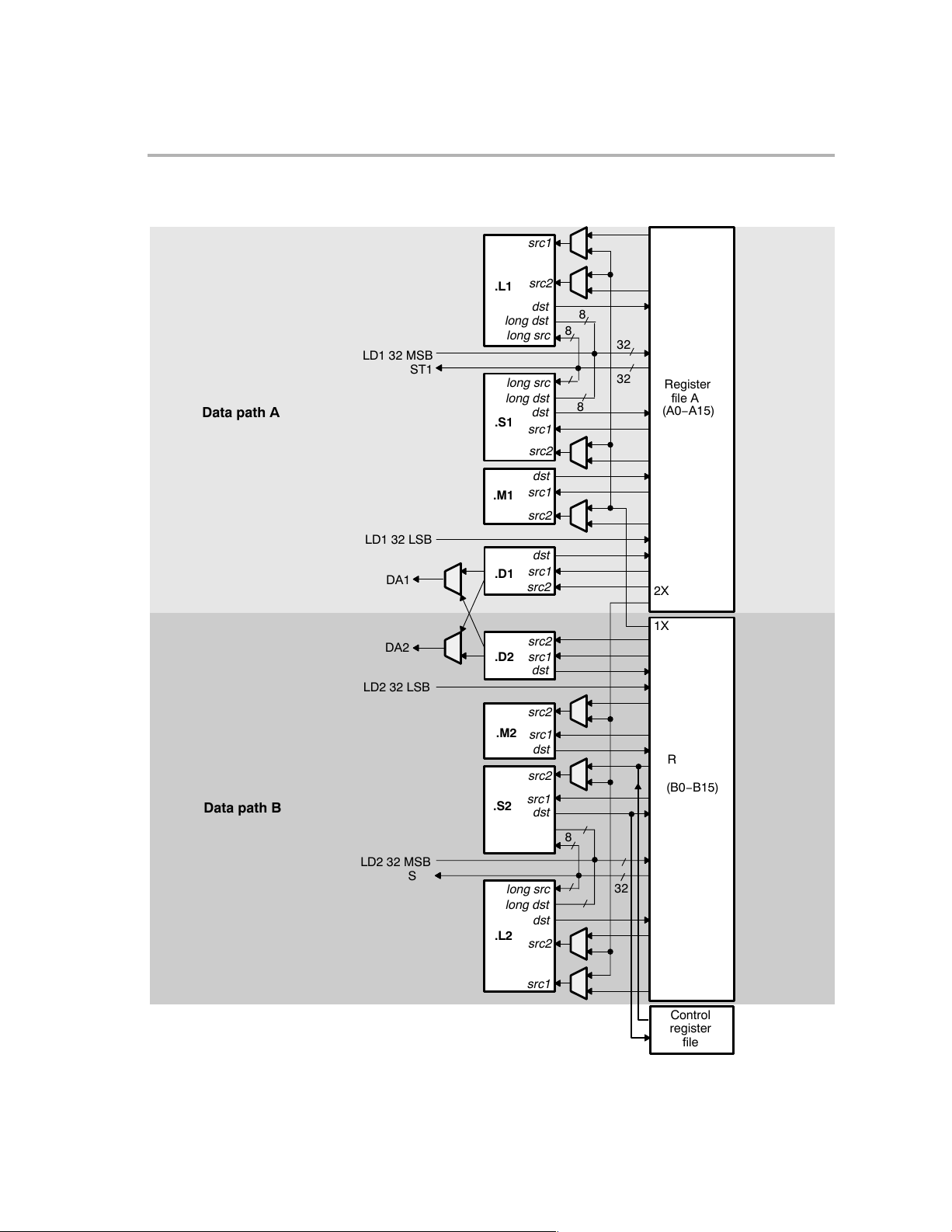
Figure 2−1. TMS320C67x CPU Data Paths
LD1 32 MSB
ST1
Data path A
LD1 32 LSB
DA1
.L1
long dst
long src
long src
long dst
.S1
.M1
.D1
src1
src2
dst
dst
src1
src2
dst
src1
src2
dst
src1
src2
General-Purpose Register Files
8
8
8
32
32
8
Register
file A
(A0−A15)
2X
Data path B
DA2
LD2 32 LSB
LD2 32 MSB
ST2
.D2
.M2
.S2
long dst
long src
long src
long dst
.L2
src2
src1
dst
src2
src1
dst
src2
src1
dst
dst
src2
src1
1X
Register
file B
(B0−B15)
8
8
8
32
32
8
Control
register
file
2-3CPU Data Paths and ControlSPRU733
Page 30
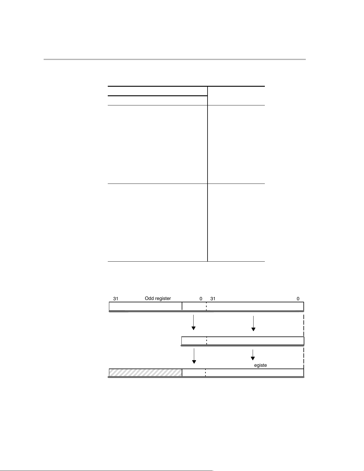
General-Purpose Register Files
Table 2−1. 40-Bit/64-Bit Register Pairs
Register Files
A B
A1:A0 B1:B0 C67x DSP
A3:A2 B3:B2
A5:A4 B5:B4
A7:A6 B7:B6
A9:A8 B9:B8
A11:A10 B11:B10
A13:A12 B13:B12
A15:A14 B15:B14
A17:A16 B17:B16 C67x+ DSP only
A19:A18 B19:B18
A21:A20 B21:B20
A23:A22 B23:B22
A25:A24 B25:B24
A27:A26 B27:B26
A29:A28 B29:B28
A31:A30 B31:B30
Devices
Figure 2−2. Storage Scheme for 40-Bit Data in a Register Pair
31 0 31 0
Odd register Even register
Ignored
Odd register Even register
Zero-filled
CPU Data Paths and Control2-4 SPRU733
78
Read from registers
39 32 31 0
Write to registers
39 32 31 0
40-bit data
40-bit data
Page 31

2.3 Functional Units
The eight functional units in the C6000 data paths can be divided into two
groups of four; each functional unit in one data path is almost identical to the
corresponding unit in the other data path. The functional units are described
in Table 2−2.
Most data lines in the CPU support 32-bit operands, and some support long
(40-bit) and double word (64-bit) operands. Each functional unit has its own
32-bit write port into a general-purpose register file (Refer to Figure 2−1). All
units ending in 1 (for example, .L1) write to register file A, and all units ending
in 2 write to register file B. Each functional unit has two 32-bit read ports for
source operands src1 and src2. Four units (.L1, .L2, .S1, and .S2) have an
extra 8-bit-wide port for 40-bit long writes, as well as an 8-bit input for 40-bit
long reads. Because each unit has its own 32-bit write port, when performing
32-bit operations all eight units can be used in parallel every cycle.
See Appendix B for a list of the instructions that execute on each functional
unit.
Table 2−2. Functional Units and Operations Performed
Functional Units
Functional Unit Fixed-Point Operations Floating-Point Operations
.L unit (.L1, .L2) 32/40-bit arithmetic and compare operations
32-bit logical operations
Leftmost 1 or 0 counting for 32 bits
Normalization count for 32 and 40 bits
.S unit (.S1, .S2) 32-bit arithmetic operations
32/40-bit shifts and 32-bit bit-field operations
32-bit logical operations
Branches
Constant generation
Register transfers to/from control register
file (.S2 only)
.M unit (.M1, .M2) 16 × 16-bit multiply operations
32 × 32-bit multiply operations
.D unit (.D1, .D2) 32-bit add, subtract, linear and circular
address calculation
Loads and stores with 5-bit constant offset
Loads and stores with 15-bit constant
offset (.D2 only)
Arithmetic operations
→ SP, INT → DP, INT → SP
DP
conversion operations
Compare
Reciprocal and reciprocal square-root
operations
Absolute value operations
→ DP conversion operations
SP
SPand DP adds and subtracts
SP and DP reverse subtracts (src2 − src1)
Floating-point multiply operations
Mixed-precision multiply operations
Load doubleword with 5-bit constant
offset
2-5CPU Data Paths and ControlSPRU733
Page 32

Register File Cross Paths
Register File Cross Paths / Memory, Load, and Store Paths
2.4 Register File Cross Paths
Each functional unit reads directly from and writes directly to the register file
within its own data path. That is, the .L1, .S1, .D1, and .M1 units write to register
file A and the .L2, .S2, .D2, and .M2 units write to register file B. The register
files are connected to the opposite-side register file’s functional units via the
1X and 2X cross paths. These cross paths allow functional units from one data
path to access a 32-bit operand from the opposite side register file. The 1X
cross path allows the functional units of data path A to read their source from
register file B, and the 2X cross path allows the functional units of data path
B to read their source from register file A.
On the C67x DSP, six of the eight functional units have access to the register
file on the opposite side, via a cross path. The .M1, .M2, .S1, and .S2 units’ src2
units are selectable between the cross path and the same side register file. In
the case of the .L1 and .L2, both src1 and src2 inputs are also selectable
between the cross path and the same-side register file.
Only two cross paths, 1X and 2X, exist in the C6000 architecture. Thus, the
limit is one source read from each data path’s opposite register file per cycle,
or a total of two cross path source reads per cycle. In the C67x DSP, only one
functional unit per data path, per execute packet, can get an operand from the
opposite register file.
2.5 Memory, Load, and Store Paths
The C67x DSP has two 32-bit paths for loading data from memory to the register file: LD1 for register file A, and LD2 for register file B. The C67x DSP also
has a second 32-bit load path for both register files A and B. This allows the
LDDW instruction to simultaneously load two 32-bit values into register file A
and two 32-bit values into register file B. For side A, LD1a is the load path for
the 32 LSBs and LD1b is the load path for the 32 MSBs. For side B, LD2a is
the load path for the 32 LSBs and LD2b is the load path for the 32 MSBs. There
are also two 32-bit paths, ST1 and ST2, for storing register values to memory
from each register file.
On the C6000 architecture, some of the ports for long and doubleword operands are shared between functional units. This places a constraint on which
long or doubleword operations can be scheduled on a data path in the same
execute packet. See section 3.7.5.
CPU Data Paths and Control2-6 SPRU733
Page 33

2.6 Data Address Paths
The data address paths (DA1 and DA2) are each connected to the .D units in
both data paths. This allows data addresses generated by any one path to
access data to or from any register.
The DA1 and DA2 resources and their associated data paths are specified as
T1 and T2, respectively. T1 consists of the DA1 address path and the LD1 and
ST1 data paths. For the C67x DSP, LD1 is comprised of LD1a and LD1b to
support 64-bit loads. Similarly, T2 consists of the DA2 address path and the
LD2 and ST2 data paths. For the C67x DSP, LD2 is comprised of LD2a and
LD2b to support 64-bit loads.
The T1 and T2 designations appear in the functional unit fields for load and
store instructions. For example, the following load instruction uses the .D1 unit
to generate the address but is using the LD2 path resource from DA2 to place
the data in the B register file. The use of the DA2 resource is indicated with the
T2 designation.
LDW .D1T2 *A0[3],B1
Data Address Paths / Control Register File
Data Address Paths
2.7 Control Register File
Table 2−3 lists the control registers contained in the control register file.
Table 2−3. Control Registers
Acronym Register Name Section
AMR Addressing mode register 2.7.3
CSR Control status register 2.7.4
ICR Interrupt clear register 2.7.5
IER Interrupt enable register 2.7.6
IFR Interrupt flag register 2.7.7
IRP Interrupt return pointer register 2.7.8
ISR Interrupt set register 2.7.9
ISTP Interrupt service table pointer register 2.7.10
NRP Nonmaskable interrupt return pointer register 2.7.11
PCE1
Program counter, E1 phase 2.7.12
2-7CPU Data Paths and ControlSPRU733
Page 34

Control Register File
2.7.1 Register Addresses for Accessing the Control Registers
Table 2−4 lists the register addresses for accessing the control register file.
One unit (.S2) can read from and write to the control register file. Each control
register is accessed by the MVC instruction. See the MVC instruction description, page 3-180, for information on how to use this instruction.
Additionally, some of the control register bits are specially accessed in other
ways. For example, arrival of a maskable interrupt on an external interrupt pin,
INTm, triggers the setting of flag bit IFRm. Subsequently, when that interrupt
is processed, this triggers the clearing of IFRm and the clearing of the global
interrupt enable bit, GIE. Finally, when that interrupt processing is complete,
the B IRP instruction in the interrupt service routine restores the pre-interrupt
value of the GIE. Similarly, saturating instructions like SADD set the SAT
(saturation) bit in the control status register (CSR).
Table 2−4. Register Addresses for Accessing the Control Registers
Acronym Register Name Address Read/ Write
AMR Addressing mode register 00000 R, W
CSR Control status register 00001 R, W
FADCR Floating-point adder configuration 10010 R, W
FAUCR Floating-point auxiliary configuration 10011 R, W
FMCR Floating-point multiplier configuration 10100 R, W
ICR Interrupt clear register 00011 W
IER Interrupt enable register 00100 R, W
IFR Interrupt flag register 00010 R
IRP Interrupt return pointer 00110 R, W
ISR Interrupt set register 00010 W
ISTP Interrupt service table pointer 00101 R, W
NRP Nonmaskable interrupt return pointer 00111 R, W
PCE1
Legend: R = Readable by the MVC instruction; W = Writeable by the MVC instruction
Program counter, E1 phase 10000 R
CPU Data Paths and Control2-8 SPRU733
Page 35

2.7.2 Pipeline/Timing of Control Register Accesses
All MVC instructions are single-cycle instructions that complete their access
of the explicitly named registers in the E1 pipeline phase. This is true whether
MVC is moving a general register to a control register, or conversely. In all
cases, the source register content is read, moved through the .S2 unit, and
written to the destination register in the E1 pipeline phase.
Pipeline Stage E1
Read src2
Written dst
Control Register File
Unit in use
.S2
Even though MVC modifies the particular target control register in a single
cycle, it can take extra clocks to complete modification of the non-explicitly
named register. For example, the MVC cannot modify bits in the IFR directly.
Instead, MVC can only write 1’s into the ISR or the ICR to specify setting or
clearing, respectively, of the IFR bits. MVC completes this ISR/ICR write in a
single (E1) cycle but the modification of the IFR bits occurs one clock later. For
more information on the manipulation of ISR, ICR, and IFR, see section 2.7.9,
section 2.7.5, and section 2.7.7.
Saturating instructions, such as SADD, set the saturation flag bit (SAT) in CSR
indirectly. As a result, several of these instructions update the SAT bit one full
clock cycle after their primary results are written to the register file. For example, the SMPY instruction writes its result at the end of pipeline stage E2; its
primary result is available after one delay slot. In contrast, the SAT bit in CSR
is updated one cycle later than the result is written; this update occurs after two
delay slots. (For the specific behavior of an instruction, refer to the description
of that individual instruction).
The B IRP and B NRP instructions directly update the GIE and NMIE,
respectively. Because these branches directly modify CSR and IER,
respectively, there are no delay slots between when the branch is issued and
when the control register updates take effect.
2-9CPU Data Paths and ControlSPRU733
Page 36

Control Register File
2.7.3 Addressing Mode Register (AMR)
For each of the eight registers (A4–A7, B4–B7) that can perform linear or circular addressing, the addressing mode register (AMR) specifies the addressing
mode. A 2-bit field for each register selects the address modification mode:
linear (the default) or circular mode. With circular addressing, the field also
specifies which BK (block size) field to use for a circular buffer. In addition, the
buffer must be aligned on a byte boundary equal to the block size. The mode
select fields and block size fields are shown in Figure 2−3 and described in
Table 2−5.
Figure 2−3. Addressing Mode Register (AMR)
31 26 25 21 20 16
Reserved
R-0 R/W-0 R/W-0
15 14 13 12 11 10 9 8 7 6 5 4 3 2 1 0
B7 MODE
R/W-0 R/W-0 R/W-0 R/W-0 R/W-0 R/W-0 R/W-0 R/W-0
Legend: R = Readable by the MVC instruction; W = Writeable by the MVC instruction; -n = value after reset
B6 MODE B5 MODE B4 MODE A7 MODE A6 MODE A5 MODE A4 MODE
BK1 BK0
Table 2−5. Addressing Mode Register (AMR) Field Descriptions
Bit Field Value Description
31−26 Reserved 0 Reserved. The reserved bit location is always read as 0. A value written to
this field has no effect.
25−21 BK1 0−1Fh Block size field 1. A 5-bit value used in calculating block sizes for circular
addressing. Table 2−6 shows block size calculations for all 32 possibilities.
Block size (in bytes) = 2
20−16 BK0 0−1Fh Block size field 0. A 5-bit value used in calculating block sizes for circular
addressing. Table 2−6 shows block size calculations for all 32 possibilities.
Block size (in bytes) = 2
15−14 B7 MODE 0−3h Address mode selection for register file B7.
0 Linear modification (default at reset)
1h Circular addressing using the BK0 field
2h Circular addressing using the BK1 field
3h Reserved
CPU Data Paths and Control2-10 SPRU733
(N+1)
, where N is the 5-bit value in BK1
(N+1)
, where N is the 5-bit value in BK0
Page 37

Control Register File
Table 2−5. Addressing Mode Register (AMR) Field Descriptions (Continued)
Bit DescriptionValueField
13−12 B6 MODE 0−3h Address mode selection for register file B6.
0 Linear modification (default at reset)
1h Circular addressing using the BK0 field
2h Circular addressing using the BK1 field
3h Reserved
11−10
9−8
7−6
B5 MODE 0−3h Address mode selection for register file B5.
0 Linear modification (default at reset)
1h Circular addressing using the BK0 field
2h Circular addressing using the BK1 field
3h Reserved
B4 MODE 0−3h Address mode selection for register file B4.
0 Linear modification (default at reset)
1h Circular addressing using the BK0 field
2h Circular addressing using the BK1 field
3h Reserved
A7 MODE 0−3h Address mode selection for register file A7.
0 Linear modification (default at reset)
1h Circular addressing using the BK0 field
2h Circular addressing using the BK1 field
3h Reserved
5−4
A6 MODE 0−3h Address mode selection for register file A6.
0 Linear modification (default at reset)
1h Circular addressing using the BK0 field
2h Circular addressing using the BK1 field
3h Reserved
2-11CPU Data Paths and ControlSPRU733
Page 38

Control Register File
Table 2−5. Addressing Mode Register (AMR) Field Descriptions (Continued)
Bit DescriptionValueField
3−2 A5 MODE 0−3h Address mode selection for register file a5.
0 Linear modification (default at reset)
1h Circular addressing using the BK0 field
2h Circular addressing using the BK1 field
3h Reserved
1−0
A4 MODE 0−3h Address mode selection for register file A4.
0 Linear modification (default at reset)
1h Circular addressing using the BK0 field
2h Circular addressing using the BK1 field
3h Reserved
Table 2−6. Block Size Calculations
BKn Value Block Size BKn Value Block Size
00000 2 10000 131 072
00001 4 10001 262 144
00010 8 10010
00011 16 10011
00100 32 10100
00101 64 10101
00110 128 10110
00111 256 10111
01000 512 11000
01001 1 024 11001
01010 2 048 11010
01011 4 096 11011
01100 8 192 11100
01101 16 384 11101
01110 32 768 11110
01111
524 288
1 048 576
2 097 152
4 194 304
8 388 608
16 777 216
33 554 432
67 108 864
134 217 728
268 435 456
536 870 912
1 073 741 824
2 147 483 648
65 536 11111 4 294 967 296
Note: When n is 11111, the behavior is identical to linear addressing.
CPU Data Paths and Control2-12 SPRU733
Page 39

Control Register File
2.7.4 Control Status Register (CSR)
The control status register (CSR) contains control and status bits. The CSR
is shown in Figure 2−4 and described in Table 2−7. For the PWRD, EN, PCC,
and DCC fields, see the device-specific data manual to see if it supports the
options that these fields control.
The power-down modes and their wake-up methods are programmed by the
PWRD field (bits 15−10) of CSR. The PWRD field of CSR is shown in
Figure 2−5. When writing to CSR, all bits of the PWRD field should be
configured at the same time. A logic 0 should be used when writing to the
reserved bit (bit 15) of the PWRD field.
Figure 2−4. Control Status Register (CSR)
31 24 23 16
CPU ID
R-0 R-x
REVISION ID
†
15 10 9 8 7 5 4 2 1 0
PWRD
R/W-0 R/WC-0 R-x R/W-0 R/W-0 R/W-0 R/W-0
Legend: R = Readable by the MVC instruction; W = Writeable by the MVC instruction; WC = Bit is cleared on write; -n = value
†
See the device-specific data manual for the default value of this field.
after reset; -x = value is indeterminate after reset
SAT EN PCC DCC PGIE GIE
Figure 2−5. PWRD Field of Control Status Register (CSR)
15 14 13 12 11 10
Reserved
R/W-0 R/W-0 R/W-0 R/W-0 R/W-0 R/W-0
Legend: R = Readable by the MVC instruction; W = Writeable by the MVC instruction; -n = value after reset
Enabled or nonenabled interrupt wake Enabled interrupt wake PD3 PD2 PD1
2-13CPU Data Paths and ControlSPRU733
Page 40

Control Register File
Table 2−7. Control Status Register (CSR) Field Descriptions
Bit Field Value Description
31−24 CPU ID 0−FFh Identifies the CPU of the device. Not writable by the MVC instruction.
0−1h Reserved
2h C67x CPU
3h C67x+ CPU
4h−FFh Reserved
23−16
15−10 PWRD 0−3Fh Power-down mode field. See Figure 2−5. Writable by the MVC instruction.
REVISION ID 0−FFh Identifies silicon revision of the CPU. For the most current silicon
revision information, see the device-specific data manual. Not writable
by the MVC instruction.
0 No power-down.
1h−8h Reserved
9h Power-down mode PD1; wake by an enabled interrupt.
Ah−10h Reserved
11h Power-down mode PD1; wake by an enabled or nonenabled interrupt.
12h−19h Reserved
1Ah Power-down mode PD2; wake by a device reset.
1Bh Reserved
1Ch Power-down mode PD3; wake by a device reset.
1D−3Fh Reserved
9
SAT Saturate bit. Can be cleared only by the MVC instruction and can be set
only by a functional unit. The set by a functional unit has priority over a
clear (by the MVC instruction), if they occur on the same cycle. The SAT
bit is set one full cycle (one delay slot) after a saturate occurs. The SAT
bit will not be modified by a conditional instruction whose condition is false.
0 Any unit does not perform a saturate.
1 Any unit performs a saturate.
8
EN Endian mode. Not writable by the MVC instruction.
0 Big endian
1 Little endian
CPU Data Paths and Control2-14 SPRU733
Page 41

Control Register File
Table 2−7. Control Status Register (CSR) Field Descriptions (Continued)
Bit DescriptionValueField
7−5 PCC 0−7h Program cache control mode. Writable by the MVC instruction. See the
TMS320C621x/C671x DSP Two-Level Internal Memory Reference Guide
(SPRU609).
0 Direct-mapped cache enabled
1h Reserved
2h Direct-mapped cache enabled
3h−7h Reserved
4−2
DCC 0−7h Data cache control mode. Writable by the MVC instruction. See the
TMS320C621x/C671x DSP Two-Level Internal Memory Reference Guide
(SPRU609).
0 2-way cache enabled
1h Reserved
2h 2-way cache enabled
3h−7h Reserved
1
PGIE Previous GIE (global interrupt enable). Copy of GIE bit at point when
interrupt is taken. Physically the same bit as SGIE bit in the interrupt task
state register (ITSR). Writeable by the MVC instruction.
0 Disables saving GIE bit when an interrupt is taken.
1 Enables saving GIE bit when an interrupt is taken.
0
GIE Global interrupt enable. Physically the same bit as GIE bit in the task state
register (TSR). Writable by the MVC instruction.
0 Disables all interrupts, except the reset interrupt and NMI (nonmaskable
interrupt).
1 Enables all interrupts.
2-15CPU Data Paths and ControlSPRU733
Page 42

Control Register File
2.7.5 Interrupt Clear Register (ICR)
The interrupt clear register (ICR) allows you to manually clear the maskable
interrupts (INT15−INT4) in the interrupt flag register (IFR). Writing a 1 to any
of the bits in ICR causes the corresponding interrupt flag (IFn) to be cleared
in IFR. Writing a 0 to any bit in ICR has no effect. Incoming interrupts have
priority and override any write to ICR. You cannot set any bit in ICR to affect
NMI or reset. The ISR is shown in Figure 2−6 and described in Table 2−8.
Note:
Any write to ICR (by the MVC instruction) effectively has one delay slot
because the results cannot be read (by the MVC instruction) in IFR until two
cycles after the write to ICR.
Any write to ICR is ignored by a simultaneous write to the same bit in the
interrupt set register (ISR).
Figure 2−6. Interrupt Clear Register (ICR)
31 16
Reserved
R-0
1514131211109876543 0
IC15 IC14 IC13 IC12 IC11 IC10 IC9 IC8 IC7 IC6 IC5 IC4 Reserved
W-0 R-0
Legend: R = Read only; W = Writeable by the MVC instruction; -n = value after reset
Table 2−8. Interrupt Clear Register (ICR) Field Descriptions
Bit Field Value Description
31−16 Reserved 0 Reserved. The reserved bit location is always read as 0. A value written to this
field has no effect.
15−4 ICn Interrupt clear.
0 Corresponding interrupt flag (IFn) in IFR is not cleared.
1 Corresponding interrupt flag (IFn) in IFR is cleared.
3−0
Reserved 0 Reserved. The reserved bit location is always read as 0. A value written to this
field has no effect.
CPU Data Paths and Control2-16 SPRU733
Page 43

Control Register File
2.7.6 Interrupt Enable Register (IER)
The interrupt enable register (IER) enables and disables individual interrupts.
The IER is shown in Figure 2−7 and described in Table 2−9.
Figure 2−7. Interrupt Enable Register (IER)
31 16
Reserved
R-0
15141312111098765432 10
IE15 IE14 IE13 IE12 IE11 IE10 IE9 IE8 IE7 IE6 IE5 IE4 Reserved NMIE 1
R/W-0 R-0 R/W-0 R-1
Legend: R = Readable by the MVC instruction; W = Writeable by the MVC instruction; -n = value after reset
Table 2−9. Interrupt Enable Register (IER) Field Descriptions
Bit Field Value Description
31−16 Reserved 0 Reserved. The reserved bit location is always read as 0. A value written to this
field has no effect.
15−4 IEn Interrupt enable. An interrupt triggers interrupt processing only if the
corresponding bit is set to 1.
0 Interrupt is disabled.
1 Interrupt is enabled.
3−2
Reserved 0 Reserved. The reserved bit location is always read as 0. A value written to this
field has no effect.
1 NMIE Nonmaskable interrupt enable. An interrupt triggers interrupt processing only if
the bit is set to 1.
The NMIE bit is cleared at reset. After reset, you must set the NMIE bit to
enable the NMI and to allow INT15−INT4 to be enabled by the GIE bit in CSR
and the corresponding IER bit. You cannot manually clear the NMIE bit; a write
of 0 has no effect. The NMIE bit is also cleared by the occurrence of an NMI.
0 All nonreset interrupts are disabled.
1 All nonreset interrupts are enabled. The NMIE bit is set only by completing a
B NRP instruction or by a write of 1 to the NMIE bit.
0 1 1 Reset interrupt enable. You cannot disable the reset interrupt.
2-17CPU Data Paths and ControlSPRU733
Page 44

Control Register File
2.7.7 Interrupt Flag Register (IFR)
The interrupt flag register (IFR) contains the status of INT4−INT15 and NMI
interrupt. Each corresponding bit in the IFR is set to 1 when that interrupt
occurs; otherwise, the bits are cleared to 0. If you want to check the status of
interrupts, use the MVC instruction to read the IFR. (See the MVC instruction
description, page 3-180, for information on how to use this instruction.) The
IFR is shown in Figure 2−8 and described in Table 2−10.
Figure 2−8. Interrupt Flag Register (IFR)
31 16
Reserved
R-0
15141312111098765432 10
IF15 IF14 IF13 IF12 IF11 IF10 IF9 IF8 IF7 IF6 IF5 IF4 Reserved NMIF 0
R-0 R-0 R-0 R-0
Legend: R = Readable by the MVC instruction; -n = value after reset
Table 2−10. Interrupt Flag Register (IFR) Field Descriptions
Bit Field Value Description
31−16 Reserved 0 Reserved. The reserved bit location is always read as 0. A value written to this
field has no effect.
15−4 IFn Interrupt flag. Indicates the status of the corresponding maskable interrupt. An
interrupt flag may be manually set by setting the corresponding bit (ISn) in the
interrupt set register (ISR) or manually cleared by setting the corresponding bit
(ICn) in the interrupt clear register (ICR).
0 Interrupt has not occurred.
1 Interrupt has occurred.
3−2
Reserved 0 Reserved. The reserved bit location is always read as 0. A value written to this
field has no effect.
1 NMIF Nonmaskable interrupt flag.
0 Interrupt has not occurred.
1 Interrupt has occurred.
0
0 0 Reset interrupt flag.
CPU Data Paths and Control2-18 SPRU733
Page 45

Control Register File
2.7.8 Interrupt Return Pointer Register (IRP)
The interrupt return pointer register (IRP) contains the return pointer that
directs the CPU to the proper location to continue program execution after
processing a maskable interrupt. A branch using the address in IRP (B IRP)
in your interrupt service routine returns to the program flow when interrupt
servicing is complete. The IRP is shown in Figure 2−9.
The IRP contains the 32-bit address of the first execute packet in the program
flow that was not executed because of a maskable interrupt. Although you can
write a value to IRP, any subsequent interrupt processing may overwrite that
value.
Figure 2−9. Interrupt Return Pointer Register (IRP)
31 0
IRP
R/W-x
Legend: R = Readable by the MVC instruction; W = Writeable by the MVC instruction; -x = value is indeterminate after reset
2-19CPU Data Paths and ControlSPRU733
Page 46

Control Register File
2.7.9 Interrupt Set Register (ISR)
The interrupt set register (ISR) allows you to manually set the maskable interrupts (INT15−INT4) in the interrupt flag register (IFR). Writing a 1 to any of the
bits in ISR causes the corresponding interrupt flag (IFn) to be set in IFR. Writing a 0 to any bit in ISR has no effect. You cannot set any bit in ISR to affect
NMI or reset. The ISR is shown in Figure 2−10 and described in Table 2−11.
Note:
Any write to ISR (by the MVC instruction) effectively has one delay slot
because the results cannot be read (by the MVC instruction) in IFR until two
cycles after the write to ISR.
Any write to the interrupt clear register (ICR) is ignored by a simultaneous
write to the same bit in ISR.
Figure 2−10. Interrupt Set Register (ISR)
31 16
Reserved
R-0
1514131211109876543 0
IS14 IS13 IS12 IS11 IS10 IS9 IS8 IS7 IS6 IS5 IS4 Reserved
IS15
W-0 R-0
Legend: R = Read only; W = Writeable by the MVC instruction; -n = value after reset
Table 2−11. Interrupt Set Register (ISR) Field Descriptions
Bit Field Value Description
31−16 Reserved 0 Reserved. The reserved bit location is always read as 0. A value written to this
field has no effect.
15−4 ISn Interrupt set.
0 Corresponding interrupt flag (IFn) in IFR is not set.
1 Corresponding interrupt flag (IFn) in IFR is set.
3−0
Reserved 0 Reserved. The reserved bit location is always read as 0. A value written to this
field has no effect.
CPU Data Paths and Control2-20 SPRU733
Page 47

Control Register File
2.7.10 Interrupt Service Table Pointer Register (ISTP)
The interrupt service table pointer register (ISTP) is used to locate the interrupt
service routine (ISR). The ISTB field identifies the base portion of the address
of the interrupt service table (IST) and the HPEINT field identifies the specific
interrupt and locates the specific fetch packet within the IST. The ISTP is
shown in Figure 2−11 and described in Table 2−12. See section 5.1.2.2 on
page 5-9 for a discussion of the use of the ISTP.
Figure 2−11.Interrupt Service Table Pointer Register (ISTP)
31 16
ISTB
R/W-0
15 109 543210
ISTB
R/W-0 R-0 R-0
Legend: R = Readable by the MVC instruction; W = Writeable by the MVC instruction; -n = value after reset
HPEINT 0 0 0 0 0
Table 2−12. Interrupt Service Table Pointer Register (ISTP) Field Descriptions
Bit Field Value Description
31−10 ISTB 0−3F FFFFh Interrupt service table base portion of the IST address. This field is cleared
to 0 on reset; therefore, upon startup the IST must reside at address 0. After
reset, you can relocate the IST by writing a new value to ISTB. If relocated,
the first ISFP (corresponding to RESET
processing, because reset clears the ISTB to 0. See Example 5−1.
9−5 HPEINT 0−1Fh Highest priority enabled interrupt that is currently pending. This field indicates
the number (related bit position in the IFR) of the highest priority interrupt (as
defined in Table 5−1 on page 5-3) that is enabled by its bit in the IER. Thus,
the ISTP can be used for manual branches to the highest priority enabled interrupt. If no interrupt is pending and enabled, HPEINT contains the value 0.
The corresponding interrupt need not be enabled by NMIE (unless it is NMI)
or by GIE.
4−0 − 0 Cleared to 0 (fetch packets must be aligned on 8-word (32-byte) boundaries).
) is never executed via interrupt
2-21CPU Data Paths and ControlSPRU733
Page 48

Control Register File
2.7.11 Nonmaskable Interrupt (NMI) Return Pointer Register (NRP)
The NMI return pointer register (NRP) contains the return pointer that directs
the CPU to the proper location to continue program execution after NMI
processing. A branch using the address in NRP (B NRP) in your interrupt
service routine returns to the program flow when NMI servicing is complete.
The NRP is shown in Figure 2−12.
The NRP contains the 32-bit address of the first execute packet in the program
flow that was not executed because of a nonmaskable interrupt. Although you
can write a value to NRP, any subsequent interrupt processing may overwrite
that value.
Figure 2−12. NMI Return Pointer Register (NRP)
31 0
NRP
R/W-x
Legend: R = Readable by the MVC instruction; W = Writeable by the MVC instruction; -x = value is indeterminate after reset
2.7.12 E1 Phase Program Counter (PCE1)
The E1 phase program counter (PCE1), shown in Figure 2−13, contains the
32-bit address of the fetch packet in the E1 pipeline phase.
Figure 2−13. E1 Phase Program Counter (PCE1)
31 0
PCE1
R-x
Legend: R = Readable by the MVC instruction; -x = value is indeterminate after reset
CPU Data Paths and Control2-22 SPRU733
Page 49

2.8 Control Register File Extensions
The C67x DSP has three additional configuration registers to support floatingpoint operations. The registers specify the desired floating-point rounding
mode for the .L and .M units. They also contain fields to warn if src1 and src2
are NaN or denormalized numbers, and if the result overflows, underflows, is
inexact, infinite, or invalid. There are also fields to warn if a divide by 0 was
performed, or if a compare was attempted with a NaN source. Table 2−13 lists
the additional registers used. The OVER, UNDER, INEX, INVAL, DENn,
NANn, INFO, UNORD and DIV0 bits within these registers will not be modified
by a conditional instruction whose condition is false.
Table 2−13. Control Register File Extensions
Acronym Register Name Section
FADCR Floating-point adder configuration register 2.8.1
FAUCR Floating-point auxiliary configuration register 2.8.2
Control Register File Extensions
FMCR
Floating-point multiplier configuration register 2.8.3
2.8.1 Floating-Point Adder Configuration Register (FADCR)
The floating-point adder configuration register (FADCR) contains fields that
specify underflow or overflow, the rounding mode, NaNs, denormalized
numbers, and inexact results for instructions that use the .L functional units.
FADCR has a set of fields specific to each of the .L units: .L2 uses bits 31−16
and .L1 uses bits 15−0. FADCR is shown in Figure 2−14 and described in
Table 2−14.
Note:
For the C67x+ DSP, the ADDSP, ADDDP, SUBSP, and SUBDP instructions
executing in the .S functional unit use the rounding mode from and set the
warning bits in FADCR. The warning bits in FADCR are the logical-OR of the
warnings produced on the .L functional unit and the warnings produced by
the ADDSP/ADDDP/SUBSP/SUBDP instructions on the .S functional unit
(but not other instructions executing on the .S functional unit).
2-23CPU Data Paths and ControlSPRU733
Page 50

Control Register File Extensions
Figure 2−14. Floating-Point Adder Configuration Register (FADCR)
31 27 26 25 24 23 22 21 20 19 18 17 16
Reserved
R-0 R/W-0 R/W-0 R/W-0 R/W-0 R/W-0 R/W-0 R/W-0 R/W-0 R/W-0 R/W-0
15 111098 76543210
Reserved
R-0 R/W-0 R/W-0 R/W-0 R/W-0 R/W-0 R/W-0 R/W-0 R/W-0 R/W-0 R/W-0
Legend: R = Readable by the MVC instruction; W = Writeable by the MVC instruction; -n = value after reset
RMODE UNDER INEX OVER INFO INVAL DEN2 DEN1 NAN2 NAN1
RMODE UNDER INEX OVER INFO INVAL DEN2 DEN1 NAN2 NAN1
Table 2−14. Floating-Point Adder Configuration Register (FADCR)
Field Descriptions
Bit Field Value Description
31−27 Reserved 0 Reserved. The reserved bit location is always read as 0. A value written to this
field has no effect.
26−25 RMODE 0−3h Rounding mode select for .L2.
0 Round toward nearest representable floating-point number
1h Round toward 0 (truncate)
2h Round toward infinity (round up)
3h Round toward negative infinity (round down)
24
UNDER Result underflow status for .L2.
0 Result does not underflow.
1 Result underflows.
23
INEX Inexact results status for .L2.
0
1 Result differs from what would have been computed had the exponent range
and precision been unbounded; never set with INVAL.
22
OVER Result overflow status for .L2.
0 Result does not overflow.
1 Result overflows.
21
INFO Signed infinity for .L2.
0 Result is not signed infinity.
1 Result is signed infinity.
CPU Data Paths and Control2-24 SPRU733
Page 51

Control Register File Extensions
Table 2−14. Floating-Point Adder Configuration Register (FADCR)
Field Descriptions (Continued)
Bit DescriptionValueField
20 INVAL
0 A signed NaN (SNaN) is not a source.
1 A signed NaN (SNaN) is a source. NaN is a source in a floating-point to integer
conversion or when infinity is subtracted from infinity.
19
DEN2 Denormalized number select for .L2 src2.
0 src2 is not a denormalized number.
1 src2 is a denormalized number.
18
DEN1 Denormalized number select for .L2 src1.
0 src1 is not a denormalized number.
1 src1 is a denormalized number.
17
NAN2 NaN select for .L2 src2.
0 src2 is not NaN.
1 src2 is NaN.
16
NAN1 NaN select for .L2 src1.
0 src1 is not NaN.
1 src1 is NaN.
15−11
10−9 RMODE 0−3h Rounding mode select for .L1.
Reserved 0 Reserved. The reserved bit location is always read as 0. A value written to this
field has no effect.
0 Round toward nearest representable floating-point number
1h Round toward 0 (truncate)
2h Round toward infinity (round up)
3h Round toward negative infinity (round down)
8
UNDER Result underflow status for .L1.
0 Result does not underflow.
1 Result underflows.
2-25CPU Data Paths and ControlSPRU733
Page 52

Control Register File Extensions
Table 2−14. Floating-Point Adder Configuration Register (FADCR)
Field Descriptions (Continued)
Bit DescriptionValueField
7 INEX Inexact results status for .L1.
0
1 Result differs from what would have been computed had the exponent range
and precision been unbounded; never set with INVAL.
6
OVER Result overflow status for .L1.
0 Result does not overflow.
1 Result overflows.
5
INFO Signed infinity for .L1.
0 Result is not signed infinity.
1 Result is signed infinity.
4
INVAL
0 A signed NaN (SNaN) is not a source.
1 A signed NaN (SNaN) is a source. NaN is a source in a floating-point to integer
conversion or when infinity is subtracted from infinity.
3
DEN2 Denormalized number select for .L1 src2.
0 src2 is not a denormalized number.
1 src2 is a denormalized number.
2
DEN1 Denormalized number select for .L1 src1.
0 src1 is not a denormalized number.
1 src1 is a denormalized number.
1
NAN2 NaN select for .L1 src2.
0 src2 is not NaN.
1 src2 is NaN.
0
NAN1 NaN select for .L1 src1.
0 src1 is not NaN.
1 src1 is NaN.
CPU Data Paths and Control2-26 SPRU733
Page 53

Control Register File Extensions
2.8.2 Floating-Point Auxiliary Configuration Register (FAUCR)
The floating-point auxiliary register (FAUCR) contains fields that specify
underflow or overflow, the rounding mode, NaNs, denormalized numbers, and
inexact results for instructions that use the .S functional units. FAUCR has a
set of fields specific to each of the .S units: .S2 uses bits 31−16 and .S1 uses
bits 15−0. FAUCR is shown in Figure 2−15 and described in Table 2−15.
Note:
For the C67x+ DSP, the ADDSP, ADDDP, SUBSP, and SUBDP instructions
executing in the .S functional unit use the rounding mode from and set the
warning bits in the floating-point adder configuration register (FADCR). The
warning bits in FADCR are the logical-OR of the warnings produced on the
.L functional unit and the warnings produced by the ADDSP/ADDDP/
SUBSP/SUBDP instructions on the .S functional unit (but not other instructions executing on the .S functional unit).
Figure 2−15. Floating-Point Auxiliary Configuration Register (FAUCR)
31 27 26 25 24 23 22 21 20 19 18 17 16
Reserved
R-0 R/W-0 R/W-0 R/W-0 R/W-0 R/W-0 R/W-0 R/W-0 R/W-0 R/W-0 R/W-0 R/W-0
15 11109 8 76543210
Reserved
R-0 R/W-0 R/W-0 R/W-0 R/W-0 R/W-0 R/W-0 R/W-0 R/W-0 R/W-0 R/W-0 R/W-0
Legend: R = Readable by the MVC instruction; W = Writeable by the MVC instruction; -n = value after reset
DIV0 UNORD UND INEX OVER INFO INVAL DEN2 DEN1 NAN2 NAN1
DIV0 UNORD UND INEX OVER INFO INVAL DEN2 DEN1 NAN2 NAN1
Table 2−15. Floating-Point Auxiliary Configuration Register (FAUCR)
Field Descriptions
Bit Field Value Description
31−27 Reserved 0 Reserved. The reserved bit location is always read as 0. A value written to this
field has no effect.
26 DIV0 Source to reciprocal operation for .S2.
0 0 is not source to reciprocal operation.
1 0 is source to reciprocal operation.
2-27CPU Data Paths and ControlSPRU733
Page 54

Control Register File Extensions
Table 2−15. Floating-Point Auxiliary Configuration Register (FAUCR)
Field Descriptions (Continued)
Bit DescriptionValueField
25 UNORD Source to a compare operation for .S2
0 NaN is not a source to a compare operation.
1 NaN is a source to a compare operation.
24
UND Result underflow status for .S2.
0 Result does not underflow.
1 Result underflows.
23
INEX Inexact results status for .S2.
0
1 Result differs from what would have been computed had the exponent range
and precision been unbounded; never set with INVAL.
22
OVER Result overflow status for .S2.
0 Result does not overflow.
1 Result overflows.
21
INFO Signed infinity for .S2.
0 Result is not signed infinity.
1 Result is signed infinity.
20
INVAL
0 A signed NaN (SNaN) is not a source.
1 A signed NaN (SNaN) is a source. NaN is a source in a floating-point to integer
conversion or when infinity is subtracted from infinity.
19
DEN2 Denormalized number select for .S2 src2.
0 src2 is not a denormalized number.
1 src2 is a denormalized number.
18
DEN1 Denormalized number select for .S2 src1.
0 src1 is not a denormalized number.
1 src1 is a denormalized number.
CPU Data Paths and Control2-28 SPRU733
Page 55

Control Register File Extensions
Table 2−15. Floating-Point Auxiliary Configuration Register (FAUCR)
Field Descriptions (Continued)
Bit DescriptionValueField
17 NAN2 NaN select for .S2 src2.
0 src2 is not NaN.
1 src2 is NaN.
16
NAN1 NaN select for .S2 src1.
0 src1 is not NaN.
1 src1 is NaN.
15−11
Reserved 0 Reserved. The reserved bit location is always read as 0. A value written to this
field has no effect.
10 DIV0 Source to reciprocal operation for .S1.
0 0 is not source to reciprocal operation.
1 0 is source to reciprocal operation.
9
UNORD Source to a compare operation for .S1
0 NaN is not a source to a compare operation.
1 NaN is a source to a compare operation.
8
UND Result underflow status for .S1.
0 Result does not underflow.
1 Result underflows.
7
INEX Inexact results status for .S1.
0
1 Result differs from what would have been computed had the exponent range
and precision been unbounded; never set with INVAL.
6
OVER Result overflow status for .S1.
0 Result does not overflow.
1 Result overflows.
2-29CPU Data Paths and ControlSPRU733
Page 56

Control Register File Extensions
Table 2−15. Floating-Point Auxiliary Configuration Register (FAUCR)
Field Descriptions (Continued)
Bit DescriptionValueField
5 INFO Signed infinity for .S1.
0 Result is not signed infinity.
1 Result is signed infinity.
4
INVAL
0 A signed NaN (SNaN) is not a source.
1 A signed NaN (SNaN) is a source. NaN is a source in a floating-point to integer
conversion or when infinity is subtracted from infinity.
3
DEN2 Denormalized number select for .S1 src2.
0 src2 is not a denormalized number.
1 src2 is a denormalized number.
2
DEN1 Denormalized number select for .S1 src1.
0 src1 is not a denormalized number.
1 src1 is a denormalized number.
1
NAN2 NaN select for .S1 src2.
0 src2 is not NaN.
1 src2 is NaN.
0
NAN1 NaN select for .S1 src1.
0 src1 is not NaN.
1 src1 is NaN.
CPU Data Paths and Control2-30 SPRU733
Page 57

Control Register File Extensions
2.8.3 Floating-Point Multiplier Configuration Register (FMCR)
The floating-point multiplier configuration register (FMCR) contains fields that
specify underflow or overflow, the rounding mode, NaNs, denormalized
numbers, and inexact results for instructions that use the .M functional units.
FMCR has a set of fields specific to each of the .M units: .M2 uses bits 31−16
and .M1 uses bits 15−0. FMCR is shown in Figure 2−16 and described in
Table 2−16.
Figure 2−16. Floating-Point Multiplier Configuration Register (FMCR)
31 27 26 25 24 23 22 21 20 19 18 17 16
Reserved
R-0 R/W-0 R/W-0 R/W-0 R/W-0 R/W-0 R/W-0 R/W-0 R/W-0 R/W-0 R/W-0
15 111098 76543210
Reserved
R-0 R/W-0 R/W-0 R/W-0 R/W-0 R/W-0 R/W-0 R/W-0 R/W-0 R/W-0 R/W-0
RMODE UNDER INEX OVER INFO INVAL DEN2 DEN1 NAN2 NAN1
RMODE UNDER INEX OVER INFO INVAL DEN2 DEN1 NAN2 NAN1
Legend: R = Readable by the MVC instruction; W = Writeable by the MVC instruction; -n = value after reset
Table 2−16. Floating-Point Multiplier Configuration Register (FMCR)
Field Descriptions
Bit Field Value Description
31−27 Reserved 0 Reserved. The reserved bit location is always read as 0. A value written to this
field has no effect.
26−25 RMODE 0−3h Rounding mode select for .M2.
0 Round toward nearest representable floating-point number
1h Round toward 0 (truncate)
2h Round toward infinity (round up)
3h Round toward negative infinity (round down)
24
UNDER Result underflow status for .M2.
0 Result does not underflow.
1 Result underflows.
2-31CPU Data Paths and ControlSPRU733
Page 58

Control Register File Extensions
Table 2−16. Floating-Point Multiplier Configuration Register (FMCR)
Field Descriptions (Continued)
Bit DescriptionValueField
23 INEX Inexact results status for .M2.
0
1 Result differs from what would have been computed had the exponent range
and precision been unbounded; never set with INVAL.
22
OVER Result overflow status for .M2.
0 Result does not overflow.
1 Result overflows.
21
INFO Signed infinity for .M2.
0 Result is not signed infinity.
1 Result is signed infinity.
20
INVAL
0 A signed NaN (SNaN) is not a source.
1 A signed NaN (SNaN) is a source. NaN is a source in a floating-point to integer
conversion or when infinity is subtracted from infinity.
19
DEN2 Denormalized number select for .M2 src2.
0 src2 is not a denormalized number.
1 src2 is a denormalized number.
18
DEN1 Denormalized number select for .M2 src1.
0 src1 is not a denormalized number.
1 src1 is a denormalized number.
17
NAN2 NaN select for .M2 src2.
0 src2 is not NaN.
1 src2 is NaN.
16
NAN1 NaN select for .M2 src1.
0 src1 is not NaN.
1 src1 is NaN.
CPU Data Paths and Control2-32 SPRU733
Page 59

Control Register File Extensions
Table 2−16. Floating-Point Multiplier Configuration Register (FMCR)
Field Descriptions (Continued)
Bit DescriptionValueField
15−11 Reserved 0 Reserved. The reserved bit location is always read as 0. A value written to this
field has no effect.
10−9 RMODE 0−3h Rounding mode select for .M1.
0 Round toward nearest representable floating-point number
1h Round toward 0 (truncate)
2h Round toward infinity (round up)
3h Round toward negative infinity (round down)
8
UNDER Result underflow status for .M1.
0 Result does not underflow.
1 Result underflows.
7
INEX Inexact results status for .M1.
0
1 Result differs from what would have been computed had the exponent range
and precision been unbounded; never set with INVAL.
6
OVER Result overflow status for .M1.
0 Result does not overflow.
1 Result overflows.
5
INFO Signed infinity for .M1.
0 Result is not signed infinity.
1 Result is signed infinity.
4
INVAL
0 A signed NaN (SNaN) is not a source.
1 A signed NaN (SNaN) is a source. NaN is a source in a floating-point to integer
conversion or when infinity is subtracted from infinity.
DEN2 Denormalized number select for .M1 src2.
3
0 src2 is not a denormalized number.
1 src2 is a denormalized number.
2-33CPU Data Paths and ControlSPRU733
Page 60

Control Register File Extensions
Table 2−16. Floating-Point Multiplier Configuration Register (FMCR)
Field Descriptions (Continued)
Bit DescriptionValueField
2 DEN1 Denormalized number select for .M1 src1.
0 src1 is not a denormalized number.
1 src1 is a denormalized number.
1
NAN2 NaN select for .M1 src2.
0 src2 is not NaN.
1 src2 is NaN.
0
NAN1 NaN select for .M1 src1.
0 src1 is not NaN.
1 src1 is NaN.
CPU Data Paths and Control2-34 SPRU733
Page 61

Chapter 3
Instruction Set
This chapter describes the assembly language instructions of the
TMS320C67x DSP. Also described are parallel operations, conditional
operations, resource constraints, and addressing modes.
The C67x floating-point DSP uses all of the instructions available to the
TMS320C62x™ DSP but it also uses other instructions that are specific to the
C67x DSP. These specific instructions are for 32-bit integer multiply, doubleword load, and floating-point operations, including addition, subtraction, and
multiplication.
Topic Page
3.1 Instruction Operation and Execution Notations 3-2. . . . . . . . . . . . . . . . . .
3.2 Instruction Syntax and Opcode Notations 3-7. . . . . . . . . . . . . . . . . . . . . . .
3.3 Overview of IEEE Standard Single- and Double-Precision Formats 3-9
3.4 Delay Slots 3-14. . . . . . . . . . . . . . . . . . . . . . . . . . . . . . . . . . . . . . . . . . . . . . . . . .
3.5 Parallel Operations 3-16. . . . . . . . . . . . . . . . . . . . . . . . . . . . . . . . . . . . . . . . . . .
3.6 Conditional Operations 3-19. . . . . . . . . . . . . . . . . . . . . . . . . . . . . . . . . . . . . . .
3.7 Resource Constraints 3-20. . . . . . . . . . . . . . . . . . . . . . . . . . . . . . . . . . . . . . . .
3.8 Addressing Modes 3-30. . . . . . . . . . . . . . . . . . . . . . . . . . . . . . . . . . . . . . . . . . .
3.9 Instruction Compatibility 3-34. . . . . . . . . . . . . . . . . . . . . . . . . . . . . . . . . . . . .
3.10 Instruction Descriptions 3-34. . . . . . . . . . . . . . . . . . . . . . . . . . . . . . . . . . . . . .
3-1Instruction SetSPRU733
Page 62

Instruction Operation and Execution Notations
3.1 Instruction Operation and Execution Notations
Table 3−1 explains the symbols used in the instruction descriptions.
Table 3−1. Instruction Operation and Execution Notations
Symbol Meaning
abs(x) Absolute value of x
and Bitwise AND
−a Perform 2s-complement subtraction using the addressing mode defined by the AMR
+a Perform 2s-complement addition using the addressing mode defined by the AMR
b
i
bit_count Count the number of bits that are 1 in a specified byte
bit_reverse Reverse the order of bits in a 32-bit register
byte0 8-bit value in the least-significant byte position in 32-bit register (bits 0-7)
byte1 8-bit value in the next to least-significant byte position in 32-bit register (bits 8-15)
byte2 8-bit value in the next to most-significant byte position in 32-bit register (bits 16-23)
byte3 8-bit value in the most-significant byte position in 32-bit register (bits 24-31)
bv2 Bit vector of two flags for s2 or u2 data type
bv4 Bit vector of four flags for s4 or u4 data type
b
y..z
cond Check for either creg equal to 0 or creg not equal to 0
creg 3-bit field specifying a conditional register, see section 3.6
cstn n-bit constant field (for example, cst5)
dint 64-bit integer value (two registers)
dp Double-precision floating-point register value
Select bit i of source/destination b
Selection of bits y through z of bit string b
dp(x) Convert x to dp
dst_h or dst_o msb32 of dst (placed in odd-numbered register of 64-bit register pair)
dst_l or dst_e lsb32 of dst (placed in even-numbered register of a 64-bit register pair)
dws4 Four packed signed 16-bit integers in a 64-bit register pair
dwu4
Four packed unsigned 16-bit integers in a 64-bit register pair
Instruction Set3-2 SPRU733
Page 63

Instruction Operation and Execution Notations
Table 3−1. Instruction Operation and Execution Notations (Continued)
Symbol Meaning
gmpy Galois Field Multiply
i2 Two packed 16-bit integers in a single 32-bit register
i4 Four packed 8-bit integers in a single 32-bit register
int 32-bit integer value
int(x) Convert x to integer
lmb0(x) Leftmost 0 bit search of x
lmb1(x) Leftmost 1 bit search of x
long 40-bit integer value
lsbn or LSBn n least-significant bits (for example, lsb16)
msbn or MSBn n most-significant bits (for example, msb16)
nop No operation
norm(x) Leftmost nonredundant sign bit of x
not Bitwise logical complement
op Opfields
or Bitwise OR
R Any general-purpose register
rcp(x) Reciprocal approximation of x
ROTL Rotate left
sat Saturate
sbyte0 Signed 8-bit value in the least-significant byte position in 32-bit register (bits 0−7)
sbyte1 Signed 8-bit value in the next to least-significant byte position in 32-bit register (bits 8−15)
sbyte2 Signed 8-bit value in the next to most-significant byte position in 32-bit register (bits 16−23)
sbyte3 Signed 8-bit value in the most-significant byte position in 32-bit register (bits 24−31)
scstn n-bit signed constant field
sdint Signed 64-bit integer value (two registers)
se
Sign-extend
3-3Instruction SetSPRU733
Page 64

Instruction Operation and Execution Notations
Table 3−1. Instruction Operation and Execution Notations (Continued)
Symbol Meaning
sint Signed 32-bit integer value
slong Signed 40-bit integer value
sllong Signed 64-bit integer value
slsb16 Signed 16-bit integer value in lower half of 32-bit register
smsb16 Signed 16-bit integer value in upper half of 32-bit register
sp Single-precision floating-point register value that can optionally use cross path
sp(x) Convert x to sp
sqrcp(x) Square root of reciprocal approximation of x
src1_h msb32 of src1
src1_l lsb32 of src1
src2_h msb32 of src2
src2_l lsb32 of src2
s2 Two packed signed 16-bit integers in a single 32-bit register
s4 Four packed signed 8-bit integers in a single 32-bit register
−s Perform 2s-complement subtraction and saturate the result to the result size, if an overflow
occurs
+s Perform 2s-complement addition and saturate the result to the result size, if an overflow
occurs
ubyte0 Unsigned 8-bit value in the least-significant byte position in 32-bit register (bits 0−7)
ubyte1 Unsigned 8-bit value in the next to least-significant byte position in 32-bit register (bits 8−15)
ubyte2 Unsigned 8-bit value in the next to most-significant byte position in 32-bit register (bits 16−23)
ubyte3 Unsigned 8-bit value in the most-significant byte position in 32-bit register (bits 24−31)
ucstn n-bit unsigned constant field (for example, ucst5)
uint Unsigned 32-bit integer value
ulong Unsigned 40-bit integer value
ullong Unsigned 64-bit integer value
ulsb16
Unsigned 16-bit integer value in lower half of 32-bit register
Instruction Set3-4 SPRU733
Page 65

Instruction Operation and Execution Notations
Table 3−1. Instruction Operation and Execution Notations (Continued)
Symbol Meaning
umsb16 Unsigned 16-bit integer value in upper half of 32-bit register
u2 Two packed unsigned 16-bit integers in a single 32-bit register
u4 Four packed unsigned 8-bit integers in a single 32-bit register
x clear b,e Clear a field in x, specified by b (beginning bit) and e (ending bit)
x ext l,r Extract and sign-extend a field in x, specified by l (shift left value) and r (shift right value)
x extu l,r Extract an unsigned field in x, specified by l (shift left value) and r (shift right value)
x set b,e Set field in x to all 1s, specified by b (beginning bit) and e (ending bit)
xint 32-bit integer value that can optionally use cross path
xor Bitwise exclusive-OR
xsint Signed 32-bit integer value that can optionally use cross path
xslsb16 Signed 16 LSB of register that can optionally use cross path
xsmsb16 Signed 16 MSB of register that can optionally use cross path
xsp Single-precision floating-point register value that can optionally use cross path
xs2 Two packed signed 16-bit integers in a single 32-bit register that can optionally use cross path
xs4 Four packed signed 8-bit integers in a single 32-bit register that can optionally use cross path
xuint Unsigned 32-bit integer value that can optionally use cross path
xulsb16 Unsigned 16 LSB of register that can optionally use cross path
xumsb16 Unsigned 16 MSB of register that can optionally use cross path
xu2 Two packed unsigned 16-bit integers in a single 32-bit register that can optionally use cross path
xu4 Four packed unsigned 8-bit integers in a single 32-bit register that can optionally use cross path
→ Assignment
+ Addition
++ Increment by 1
× Multiplication
− Subtraction
==
Equal to
3-5Instruction SetSPRU733
Page 66

Instruction Operation and Execution Notations
Table 3−1. Instruction Operation and Execution Notations (Continued)
Symbol Meaning
> Greater than
>= Greater than or equal to
< Less than
<= Less than or equal to
<< Shift left
>> Shift right
>>s Shift right with sign extension
>>z Shift right with a zero fill
~ Logical inverse
&
Logical AND
Instruction Set3-6 SPRU733
Page 67

Instruction Syntax and Opcode Notations
3.2 Instruction Syntax and Opcode Notations
Table 3−2 explains the syntaxes and opcode fields used in the instruction
descriptions.
The C64x CPU 32-bit opcodes are mapped in Appendix C through Appendix G.
Table 3−2. Instruction Syntax and Opcode Notations
Symbol Meaning
baseR base address register
CC
creg 3-bit field specifying a conditional register, see section 3.6
cst constant
csta constant a
cstb constant b
cstn n-bit constant field
dst destination
dstms
dw doubleword; 0 = word, 1 = doubleword
ii
n
ld/st load or store; 0 = store, 1 = load
mode addressing mode, see section 3.8
offsetR register offset
op opfield; field within opcode that specifies a unique instruction
op
n
p parallel execution; 0 = next instruction is not executed in parallel, 1 = next instruction is
r LDDW instruction
rsv reserved
s side A or B for destination; 0 = side A, 1 = side B.
sc scaling mode; 0 = nonscaled, offsetR/ucst5 is not shifted; 1 = scaled, offsetR/ucst5 is shifted
scstn
bit n of the constant ii
bit n of the opfield
executed in parallel
n-bit signed constant field
3-7Instruction SetSPRU733
Page 68

Instruction Syntax and Opcode Notations
Table 3−2. Instruction Syntax and Opcode Notations (Continued)
Symbol Meaning
scst
n
bit n of the signed constant field
sn sign
src source
src1 source 1
src2 source 2
srcms
stg
n
bit n of the constant stg
t side of source/destination (src/dst) register; 0 = side A, 1 = side B
ucstn n-bit unsigned constant field
ucst
n
bit n of the unsigned constant field
unit unit decode
x cross path for src2; 0 = do not use cross path, 1 = use cross path
y .D1 or .D2 unit; 0 = .D1 unit, 1 = .D2 unit
z
test for equality with zero or nonzero
Instruction Set3-8 SPRU733
Page 69

Overview of IEEE Standard Single- and Double-Precision Formats
3.3 Overview of IEEE Standard Single- and Double-Precision Formats
Floating-point operands are classified as single-precision (SP) and doubleprecision (DP). Single-precision floating-point values are 32-bit values stored
in a single register. Double-precision floating-point values are 64-bit values
stored in a register pair. The register pair consists of consecutive even and odd
registers from the same register file. The 32 least-significant-bits are loaded
into the even register; the 32 most-significant-bits containing the sign bit and
exponent are loaded into the next register (that is always the odd register). The
register pair syntax places the odd register first, followed by a colon, then the
even register (that is, A1:A0, B1:B0, A3:A2, B3:B2, etc.).
Instructions that use DP sources fall in two categories: instructions that read
the upper and lower 32-bit words on separate cycles, and instructions that
read both 32-bit words on the same cycle. All instructions that produce a
double-precision result write the low 32-bit word one cycle before writing the
high 32-bit word. If an instruction that writes a DP result is followed by an
instruction that uses the result as its DP source and it reads the upper and lower words on separate cycles, then the second instruction can be scheduled on
the same cycle that the high 32-bit word of the result is written. The lower result
is written on the previous cycle. This is because the second instruction reads
the low word of the DP source one cycle before the high word of the DP source.
IEEE floating-point numbers consist of normal numbers, denormalized
numbers, NaNs (not a number), and infinity numbers. Denormalized numbers
are nonzero numbers that are smaller than the smallest nonzero normal
number. Infinity is a value that represents an infinite floating-point number.
NaN values represent results for invalid operations, such as (+infinity +
(−infinity)).
Normal single-precision values are always accurate to at least six decimal
places, sometimes up to nine decimal places. Normal double-precision values
are always accurate to at least 15 decimal places, sometimes up to 17 decimal
places.
Table 3−3 shows notations used in discussing floating-point numbers.
3-9Instruction SetSPRU733
Page 70

Overview of IEEE Standard Single- and Double-Precision Formats
Table 3−3. IEEE Floating-Point Notations
Symbol Meaning
s Sign bit
e Exponent field
f Fraction (mantissa) field
x Can have value of 0 or 1 (don’t care)
NaN Not-a-Number (SNaN or QNaN)
SNaN Signal NaN
QNaN Quiet NaN
NaN_out QNaN with all bits in the f field = 1
Inf Infinity
LFPN Largest floating-point number
SFPN Smallest floating-point number
LDFPN Largest denormalized floating-point number
SDFPN Smallest denormalized floating-point number
signed Inf +infinity or −infinity
signed NaN_out
NaN_out with s = 0 or 1
Instruction Set3-10 SPRU733
Page 71

Overview of IEEE Standard Single- and Double-Precision Formats
Á
Á
Á
Á
Á
Á
Á
Á
Figure 3−1 shows the fields of a single-precision floating-point number represented within a 32-bit register.
Figure 3−1. Single-Precision Floating-Point Fields
31
30
s
e
23 22
f
Legend: s sign bit (0 = positive, 1 = negative)
e 8-bit exponent ( 0 < e < 255)
f 23-bit fraction
0 < f < 1*2
−1
+ 1*2−2 + ... + 1*2
−23
or
0 < f < ((223)−1)/(223)
The floating-point fields represent floating-point numbers within two ranges:
normalized (e is between 0 and 255) and denormalized (e is 0). The following
formulas define how to translate the s, e, and f fields into a single-precision
floating-point number.
Normalized:
s
(e−127)
−1
× 2
× 1.f 0 < e < 255
Denormalized (Subnormal):
s
−126
−1
× 2
× 0.f e = 0; f nonzero
Table 3−4 shows the s,e, and f values for special single-precision floatingpoint numbers.
0
Table 3−4. Special Single-Precision Values
Symbol
+0
−0
+Inf
БББББ
−Inf
NaN
QNaN
БББББ
SNaN
Sign (s)
0
1
0
ÁÁÁ
1
x
x
ÁÁÁ
x
Exponent (e)
0
0
255
ÁÁÁ
255
255
255
ÁÁÁ
255
Fraction (f)
0
0
0
БББББББ
0
nonzero
1xx..x
БББББББ
0xx..x and nonzero
3-11Instruction SetSPRU733
Page 72

Overview of IEEE Standard Single- and Double-Precision Formats
Table 3−5 shows hexadecimal and decimal values for some single-precision
floating-point numbers.
Figure 3−2 shows the fields of a double-precision floating-point number represented within a pair of 32-bit registers.
Table 3−5. Hexadecimal and Decimal Representation for Selected Single-Precision Values
Symbol Hex Value Decimal Value
NaN_out 7FFF FFFF QNaN
0 0000 0000 0.0
−0 8000 0000 −0.0
1 3F80 0000 1.0
2 4000 0000 2.0
LFPN 7F7F FFFF 3.40282347e+38
SFPN 0080 0000 1.17549435e−38
LDFPN 007F FFFF 1.17549421e−38
SDFPN
0000 0001 1.40129846e−45
Figure 3−2. Double-Precision Floating-Point Fields
31
30
s
Legend: s sign bit (0 = positive, 1 = negative)
e
Odd register Even register
e 11-bit exponent ( 0 < e < 2047)
f 52-bit fraction
0 < f < 1*2
0 < f < ((2
The floating-point fields represent floating-point numbers within two ranges:
normalized (e is between 0 and 2047) and denormalized (e is 0). The following
formulas define how to translate the s, e, and f fields into a double-precision
floating-point number.
20 19 0
−1
+ 1*2−2 + ... + 1*2
52
)−1)/(252)
31
f
−52
or
f
0
Instruction Set3-12 SPRU733
Page 73

Overview of IEEE Standard Single- and Double-Precision Formats
Normalized:
s
(e−1023)
−1
× 2
× 1.f 0 < e < 2047
Denormalized (Subnormal):
s
−1022
−1
× 2
× 0.f e = 0; f nonzero
Table 3−6 shows the s, e, and f values for special double-precision floatingpoint numbers.
Table 3−6. Special Double-Precision Values
Symbol Sign (s) Exponent (e) Fraction (f)
+0 0 0 0
−0100
+Inf 0 2047 0
−Inf 1 2047 0
NaN x 2047 nonzero
QNaN x 2047 1xx..x
SNaN
x 2047 0xx..x and nonzero
Table 3−7 shows hexadecimal and decimal values for some double-precision
floating-point numbers.
Table 3−7. Hexadecimal and Decimal Representation for Selected Double-Precision Values
Symbol Hex Value Decimal Value
NaN_out 7FFF FFFF FFFF FFFF QNaN
0 0000 0000 0000 0000 0.0
−0 8000 0000 0000 0000 −0.0
1 3FF0 0000 0000 0000 1.0
2 4000 0000 0000 0000 2.0
LFPN 7FEF FFFF FFFF FFFF 1.7976931348623157e+308
SFPN 0010 0000 0000 0000 2.2250738585072014e−308
LDFPN 000F FFFF FFFF FFFF 2.2250738585072009e−308
SDFPN
0000 0000 0000 0001 4.9406564584124654e−324
3-13Instruction SetSPRU733
Page 74

Delay Slots
3.4 Delay Slots
The execution of floating-point instructions can be defined in terms of delay
slots and functional unit latency. The number of delay slots is equivalent to the
number of additional cycles required after the source operands are read for the
result to be available for reading. For a single-cycle type instruction, operands
are read on cycle i and produce a result that can be read on cycle i + 1. For
a 4-cycle instruction, operands are read on cycle i and produce a result that
can be read on cycle i + 4. Table 3−8 shows the number of delay slots associat-
ed with each type of instruction.
The double-precision floating-point addition, subtraction, multiplication,
compare, and the 32-bit integer multiply instructions also have a functional unit
latency that is greater than 1. The functional unit latency is equivalent to the
number of cycles that the instruction uses the functional unit read ports. For
example, the ADDDP instruction has a functional unit latency of 2. Operands
are read on cycle i and cycle i + 1. Therefore, a new instruction cannot begin
until cycle i + 2, rather than i + 1. ADDDP produces a result that can be read
on cycle i + 7, because it has six delay slots.
Delay slots are equivalent to an execution or result latency. All of the instructions in the C67x DSP have a functional unit latency of 1. This means that a
new instruction can be started on the functional unit each cycle. Single-cycle
throughput is another term for single-cycle functional unit latency.
Instruction Set3-14 SPRU733
Page 75

Table 3−8. Delay Slot and Functional Unit Latency
Delay Slots
Instruction Type
Delay
Slots
Functional
Unit Latency
Read Cycles
†
Cycles
Write
Single cycle 0 1 i i
2-cycle DP 1 1 i i, i + 1
DP compare 1 2 i, i + 1 1 + 1
4-cycle 3 1 i i + 3
INTDP 4 1 i i + 3, i + 4
Load 4 1 i i, i + 4
MPYSP2DP 4 2 i i + 3, i + 4
ADDDP/SUBDP 6 2 i, i + 1 i + 5, i + 6
MPYSPDP 6 3 i, i + 1 i + 5, i + 6
MPYI 8 4 i, i + 1, 1 + 2, i + 3 i + 8
MPYID 9 4 i, i + 1, 1 + 2, i + 3 i + 8, i + 9
MPYDP
†
Cycle i is in the E1 pipeline phase.
‡
A write on cycle i + 4 uses a separate write port from other .D unit instructions.
9 4 i, i + 1, 1 + 2, i + 3 i + 8, i + 9
†
‡
3-15Instruction SetSPRU733
Page 76

Parallel Operations
3.5 Parallel Operations
Instructions are always fetched eight at a time. This constitutes a fetch packet.
The basic format of a fetch packet is shown in Figure 3−3. Fetch packets are
aligned on 256-bit (8-word) boundaries.
Figure 3−3. Basic Format of a Fetch Packet
31 0 31 0 31 0 31 0 31 0 31 0 31 0 31 0
pppppppp
LSBs of
the byte
address
Instruction
A
00000b
Instruction
B
00100b
Instruction
C
01000b
Instruction
D
01100b
Instruction
E
10000b
Instruction
F
10100b
Instruction
G
11000b
Instruction
11100b
The execution of the individual instructions is partially controlled by a bit in
each instruction, the p-bit. The p-bit (bit 0) determines whether the instruction
executes in parallel with another instruction. The p-bits are scanned from left
to right (lower to higher address). If the p -bit of instruction i is 1, then instruction
i + 1 is to be executed in parallel with (in the the same cycle as) instruction i.
If the p-bit of instruction i is 0, then instruction i + 1 is executed in the cycle after
instruction i. All instructions executing in parallel constitute an execute packet.
An execute packet can contain up to eight instructions. Each instruction in an
execute packet must use a different functional unit.
On the C67x DSP, an execute packet cannot cross an 8-word boundary;
therefore, the last p-bit in a fetch packet is always cleared to 0, and each fetch
packet starts a new execute packet. On the C67x+ DSP, an execute packet
can cross an 8-word boundary.
There are three types of p-bit patterns for fetch packets. These three p-bit patterns result in the following execution sequences for the eight instructions:
H
Fully serial
Fully parallel
Partially serial
Example 3−1 through Example 3−3 show the conversion of a p-bit sequence
into a cycle-by-cycle execution stream of instructions.
Instruction Set3-16 SPRU733
Page 77

Parallel Operations
Example 3−1. Fully Serial p-Bit Pattern in a Fetch Packet
This p-bit pattern:
31 0 31 0 31 0 31 0 31 0 31 0 31 0 31 0
00000000
InstructionAInstructionBInstructionCInstructionDInstructionEInstructionFInstructionGInstruction
H
results in this execution sequence:
Cycle/Execute
Packet
1 A
2B
3C
4D
5E
6F
7G
8 H
Instructions
The eight instructions are executed sequentially.
Example 3−2. Fully Parallel p-Bit Pattern in a Fetch Packet
This p-bit pattern:
31 0 31 0 31 0 31 0
11111110
InstructionAInstructionBInstructionCInstructionDInstructionEInstructionFInstructionGInstruction
31 0 31 0 31 0 31 0
H
results in this execution sequence:
Cycle/Execute
Packet
1 A B C D E F G H
Instructions
All eight instructions are executed in parallel.
3-17Instruction SetSPRU733
Page 78

Parallel Operations
Example 3−3. Partially Serial p-Bit Pattern in a Fetch Packet
This p-bit pattern:
31 0 31 0 31 0 31 0
0011
31 0 31 0 31 0 31 0
0110
InstructionAInstructionBInstructionCInstructionDInstructionEInstructionFInstructionGInstruction
results in this execution sequence:
Cycle/Execute Packet Instructions
1 A
2 B
3
4
Note: Instructions C, D, and E do not use any of the same functional units, cross paths, or
other data path resources. This is also true for instructions F, G, and H.
CDE
F G H
3.5.1 Example Parallel Code
The vertical bars || signify that an instruction is to execute in parallel with the
previous instruction. The code for the fetch packet in Example 3−3 would be
represented as this:
instruction A
instruction B
instruction C
|| instruction D
|| instruction E
H
instruction F
|| instruction G
|| instruction H
3.5.2 Branching Into the Middle of an Execute Packet
If a branch into the middle of an execute packet occurs, all instructions at lower
addresses are ignored. In Example 3−3, if a branch to the address containing
instruction D occurs, then only D and E execute. Even though instruction C is
in the same execute packet, it is ignored. Instructions A and B are also ignored
because they are in earlier execute packets. If your result depends on executing A, B, or C, the branch to the middle of the execute packet will produce an
erroneous result.
Instruction Set3-18 SPRU733
Page 79

3.6 Conditional Operations
Most instructions can be conditional. The condition is controlled by a 3-bit
opcode field (creg) that specifies the condition register tested, and a 1-bit field
(z) that specifies a test for zero or nonzero. The four MSBs of every opcode
are creg and z. The specified condition register is tested at the beginning of
the E1 pipeline stage for all instructions. For more information on the pipeline,
see Chapter 4. If z = 1, the test is for equality with zero; if z = 0, the test is for
nonzero. The case of creg = 0 and z = 0 is treated as always true to allow
instructions to be executed unconditionally. The creg field is encoded in the
instruction opcode as shown in Table 3−9.
Table 3−9. Registers That Can Be Tested by Conditional Operations
Conditional Operations
Specified
Conditional
Register
Unconditional 0 0 0 0
Reserved
B0 001 z
B1 010 z
B2 011 z
A1 100 z
A2 101 z
Reserved
†
This value is reserved for software breakpoints that are used for emulation purposes.
‡
x can be any value.
†
Bit
31 30 29 28
000 1
1 1 x
creg z
‡
‡
x
Conditional instructions are represented in code by using square brackets, [ ],
surrounding the condition register name. The following execute packet
contains two ADD instructions in parallel. The first ADD is conditional on B0
being nonzero. The second ADD is conditional on B0 being zero. The character ! indicates the inverse of the condition.
[B0] ADD .L1 A1,A2,A3
|| [!B0] ADD .L2 B1,B2,B3
The above instructions are mutually exclusive, only one will execute. If they
are scheduled in parallel, mutually exclusive instructions are constrained as
described in section 3.7. If mutually exclusive instructions share any resources
as described in section 3.7, they cannot be scheduled in parallel (put in the
same execute packet), even though only one will execute.
3-19Instruction SetSPRU733
Page 80

Resource Constraints
3.7 Resource Constraints
No two instructions within the same execute packet can use the same
resources. Also, no two instructions can write to the same register during the
same cycle. The following sections describe how an instruction can use each
of the resources.
3.7.1 Constraints on Instructions Using the Same Functional Unit
Two instructions using the same functional unit cannot be issued in the same
execute packet.
The following execute packet is invalid:
ADD .S1 A0, A1, A2 ;.S1 is used for
|| SHR .S1 A3, 15, A4 ;...both instructions
The following execute packet is valid:
ADD .L1 A0, A1, A2 ;Two different functional
|| SHR .S1 A3, 15, A4 ;...units are used
3.7.2 Constraints on the Same Functional Unit Writing in the Same Instruction Cycle
Two instructions using the same functional unit cannot write their results in the
same instruction cycle.
Instruction Set3-20 SPRU733
Page 81

3.7.3 Constraints on Cross Paths (1X and 2X)
One unit (either a .S, .L, or .M unit) per data path, per execute packet, can read
a source operand from its opposite register file via the cross paths (1X and 2X).
For example, the .S1 unit can read both its operands from the A register file; or
it can read an operand from the B register file using the 1X cross path and the
other from the A register file. The use of a cross path is denoted by an X following
the functional unit name in the instruction syntax (as in S1X).
The following execute packet is invalid because the 1X cross path is being
used for two different B register operands:
MV .S1X B0, A0 ; \ Invalid. Instructions are using the 1X cross path
|| MV .L1X B1, A1 ; / with different B registers
The following execute packet is valid because all uses of the 1X cross path are
for the same B register operand, and all uses of the 2X cross path are for the
same A register operand:
ADD .L1X A0,B1,A1 ; \ Instructions use the 1X with B1
|| SUB .S1X A2,B1,A2 ; / 1X cross paths using B1
|| AND .D1 A4,A1,A3 ;
|| MPY .M1 A6,A1,A4 ;
|| ADD .L2 B0,B4,B2 ;
|| SUB .S2X B4,A4,B3 ; / 2X cross paths using A4
|| AND .D2X B5,A4,B4 ; / 2X cross paths using A4
|| MPY .M2 B6,B4,B5 ;
Resource Constraints
The operand comes from a register file opposite of the destination, if the x bit
in the instruction field is set.
3-21Instruction SetSPRU733
Page 82

Resource Constraints
3.7.4 Constraints on Loads and Stores
Load and store instructions can use an address pointer from one register file
while loading to or storing from the other register file. Two load and store
instructions using a destination/source from the same register file cannot be
issued in the same execute packet. The address register must be on the same
side as the .D unit used.
The following execute packet is invalid:
LDW.D1 *A0,A1 ; \ .D2 unit must use the address
|| LDW .D2 *A2,B2 ; / register from the B register file
The following execute packet is valid:
LDW.D1 *A0,A1 ; \ Address registers from correct
|| LDW .D2 *B0,B2 ; / register files
Two loads and/or stores loading to and/or storing from the same register file
cannot be issued in the same execute packet.
The following execute packet is invalid:
LDW.D1 *A4,A5 ; \ Loading to and storing from the
|| STW .D2 A6,*B4 ; / same register file
The following execute packets are valid:
LDW.D1 *A4,B5 ; \ Loading to, and storing from
|| STW .D2 A6,*B4 ; / different register files
LDW.D1 *A0,B2 ; \ Loading to
|| LDW .D2 *B0,A1 ; / different register files
Instruction Set3-22 SPRU733
Page 83

3.7.5 Constraints on Long (40-Bit) Data
Because the .S and .L units share a read register port for long source operands
and a write register port for long results, only one long result may be issued
per register file in an execute packet. All instructions with a long result on the
.S and .L units have zero delay slots. See section 2.2 for the order for long
pairs.
The following execute packet is invalid:
ADD .L1 A5:A4,A1,A3:A2 ; \ Two long writes
|| SHL.S1 A8,A9,A7:A6 ; / on A register file
The following execute packet is valid:
ADD .L1 A5:A4,A1,A3:A2 ; \ One long write for
|| SHL.S2 B8,B9,B7:B6 ; / each register file
Because the .L and .S units share their long read port with the store port,
operations that read a long value cannot be issued on the .L and/or .S units
in the same execute packet as a store.
The following execute packet is invalid:
ADD .L1 A5:A4,A1,A3:A2 ; \ Long read operation and a
|| STW .D1 A8,*A9 ; / store
Resource Constraints
The following execute packet is valid:
ADD .L1 A4, A1, A3:A2 ; \ No long read with
|| STW.D1 A8,*A9 ; / the store
On the C67x DSP, doubleword load instructions conflict with long results from
the .S units. All stores conflict with a long source on the .S unit. The following
execute packet is invalid, because the .D unit store on the T1 path conflicts with
the long source on the .S1 unit:
ADD .S1 A1,A5:A4, A3:A2 ; \ Long source on .S unit and a store
|| STW .D1T1 A8,*A9 ; / on the T1 path of the .D unit
The following code sequence is invalid:
LDDW .D1T1 *A16,A11:A10 ; \ Double word load written to
; A11:A10 on .D1
NOP 3 ; conflicts after 3 cycles
SHL .S1 A8,A9,A7:A6 ; / with write to A7:A6 on .S1
The following execute packets are valid:
ADD .L1 A1,A5:A4,A3:A2 ; \ One long write for
|| SHL .S2 B8,B9,B7:B6 ; / each register file
ADD .L1 A4, A1, A3:A2 ; \ No long read with
|| STW .D1T1 A8,*A9 ; / the store on T1 path of .D1
3-23Instruction SetSPRU733
Page 84

Resource Constraints
3.7.6 Constraints on Register Reads
More than four reads of the same register cannot occur on the same cycle.
Conditional registers are not included in this count.
The following execute packets are invalid:
MPY .M1 A1, A1, A4 ; five reads of register A1
|| ADD .L1 A1, A1, A5
|| SUB .D1 A1, A2, A3
MPY .M1 A1, A1, A4 ; five reads of register A1
|| ADD .L1 A1, A1, A5
|| SUB .D2x A1, B2, B3
The following execute packet is valid:
MPY .M1 A1, A1, A4 ; only four reads of A1
|| [A1] ADD .L1 A0, A1, A5
|| SUB .D1 A1, A2, A3
Instruction Set3-24 SPRU733
Page 85

3.7.7 Constraints on Register Writes
Two instructions cannot write to the same register on the same cycle. Two
instructions with the same destination can be scheduled in parallel as long as
they do not write to the destination register on the same cycle. For example,
an MPY issued on cycle i followed by an ADD on cycle i + 1 cannot write to the
same register because both instructions write a result on cycle i + 1. Therefore,
the following code sequence is invalid unless a branch occurs after the MPY,
causing the ADD not to be issued.
MPY .M1 A0, A1, A2
ADD .L1 A4, A5, A2
However, this code sequence is valid:
MPY .M1 A0, A1, A2
|| ADD .L1 A4, A5, A2
Figure 3−4 shows different multiple-write conflicts. For example, ADD and
SUB in execute packet L1 write to the same register. This conflict is easily
detectable.
Resource Constraints
MPY in packet L2 and ADD in packet L3 might both write to B2 simultaneously;
however, if a branch instruction causes the execute packet after L2 to be
something other than L3, a conflict would not occur. Thus, the potential conflict
in L2 and L3 might not be detected by the assembler. The instructions in L4
do not constitute a write conflict because they are mutually exclusive. In
contrast, because the instructions in L5 may or may not be mutually exclusive,
the assembler cannot determine a conflict. If the pipeline does receive
commands to perform multiple writes to the same register, the result is
undefined.
Figure 3−4. Examples of the Detectability of Write Conflicts by the Assembler
L1: ADD.L2 B5,B6, B7 ; \ detectable, conflict
|| SUB.S2 B8,B9, B7 ; /
L2: MPY.M2 B0,B1, B2 ; \ not detectable
L3: ADD.L2 B3,B4, B2 ; /
L4:[!B0] ADD.L2 B5,B6, B7 ; \ detectable, no conflict
|| [B0] SUB.S2 B8,B9, B7 ; /
L5:[!B1] ADD.L2 B5,B6, B7 ; \ not detectable
|| [B0] SUB.S2 B8,B9, B7 ; /
3-25Instruction SetSPRU733
Page 86

Resource Constraints
3.7.8 Constraints on Floating-Point Instructions
If an instruction has a multicycle functional unit latency, it locks the functional
unit for the necessary number of cycles. Any new instruction dispatched to that
functional unit during this locking period causes undefined results. If an
instruction with a multicycle functional unit latency has a condition that is evaluated as false during E1, it still locks the functional unit for subsequent cycles.
An instruction of the following types scheduled on cycle i has the following
constraints:
DP compare No other instruction can use the functional unit on cycles
i and i + 1.
ADDDP/SUBDP No other instruction can use the functional unit on cycles
i and i + 1.
MPYI No other instruction can use the functional unit on cycles
i, i + 1, i + 2, and i + 3.
MPYID No other instruction can use the functional unit on cycles
i, i + 1, i + 2, and i + 3.
MPYDP No other instruction can use the functional unit on cycles
i, i + 1, i + 2, and i + 3.
MPYSPDP No other instruction can use the functional unit on cycles
i and i + 1.
MPYSP2DP No other instruction can use the functional unit on cycles
i and i + 1.
If a cross path is used to read a source in an instruction with a multicycle functional unit latency, you must ensure that no other instructions executing on the
same side uses the cross path.
An instruction of the following types scheduled on cycle i using a cross path
to read a source, has the following constraints:
DP compare No other instruction on the same side can used the cross
path on cycles i and i + 1.
ADDDP/SUBDP No other instruction on the same side can use the cross
path on cycles i and i + 1.
MPYI No other instruction on the same side can use the cross
path on cycles i, i + 1, i + 2, and i + 3.
MPYID No other instruction on the same side can use the cross
path on cycles i, i + 1, i + 2, and i + 3.
Instruction Set3-26 SPRU733
Page 87

Resource Constraints
MPYDP No other instruction on the same side can use the cross
path on cycles i, i + 1, i + 2, and i + 3.
MPYSPDP No other instruction on the same side can use the cross
path on cycles i and i + 1.
Other hazards exist because instructions have varying numbers of delay slots,
and need the functional unit read and write ports of varying numbers of cycles.
A read or write hazard exists when two instructions on the same functional unit
attempt to read or write, respectively, to the register file on the same cycle.
An instruction of the following types scheduled on cycle i has the following
constraints:
2-cycle DP A single-cycle instruction cannot be scheduled on that
functional unit on cycle i + 1 due to a write hazard on cycle
i + 1.
Another 2-cycle DP instruction cannot be scheduled on
that functional unit on cycle i + 1 due to a write hazard on
cycle i + 1.
4-cycle A single-cycle instruction cannot be scheduled on that
functional unit on cycle i + 3 due to a write hazard on cycle
i + 3.
A multiply (16 × 16-bit) instruction cannot be scheduled
on that functional unit on cycle i + 2 due to a write hazard
on cycle i + 3.
ADDDP/SUBDP A single-cycle instruction cannot be scheduled on that
functional unit on cycle i + 5 or i + 6 due to a write hazard
on cycle i + 5 or i + 6, respectively.
A 4-cycle instruction cannot be scheduled on that functional unit on cycle i + 2 or i + 3 due to a write hazard on
cycle i + 5 or i + 6, respectively.
An INTDP instruction cannot be scheduled on that functional unit on cycle i + 2 or i + 3 due to a write hazard on
cycle i + 5 or i + 6, respectively.
INTDP A single-cycle instruction cannot be scheduled on that
functional unit on cycle i + 3 or i + 4 due to a write hazard
on cycle i + 3 or i + 4, respectively.
An INTDP instruction cannot be scheduled on that functional unit on cycle i + 1 due to a write hazard on cycle
i + 1.
A 4-cycle instruction cannot be scheduled on that functional unit on cycle i + 1 due to a write hazard on cycle
i + 1.
3-27Instruction SetSPRU733
Page 88

Resource Constraints
MPYI A 4-cycle instruction cannot be scheduled on that func-
tional unit on cycle i + 4, i + 5, or i + 6.
A MPYDP instruction cannot be scheduled on that func-
tional unit on cycle i + 4, i + 5, or i + 6.
A MPYSPDP instruction cannot be scheduled on that
functional unit on cycle i + 4, i + 5, or i + 6.
A MPYSP2DP instruction cannot be scheduled on that
functional unit on cycle i + 4, i + 5, or i + 6.
A multiply (16 × 16-bit) instruction cannot be scheduled
on that functional unit on cycle i + 6 due to a write hazard
on cycle i + 7.
MPYID A 4-cycle instruction cannot be scheduled on that func-
tional unit on cycle i + 4, i + 5, or i + 6.
A MPYDP instruction cannot be scheduled on that func-
tional unit on cycle i + 4, i + 5, or i + 6.
A MPYSPDP instruction cannot be scheduled on that
functional unit on cycle i + 4, i + 5, or i + 6.
A MPYSP2DP instruction cannot be scheduled on that
functional unit on cycle i + 4, i + 5, or i + 6.
A multiply (16 × 16-bit) instruction cannot be scheduled
on that functional unit on cycle i + 7 or i + 8 due to a write
hazard on cycle i + 8 or i + 9, respectively.
MPYDP A 4-cycle instruction cannot be scheduled on that func-
tional unit on cycle i + 4, i + 5, or i + 6.
A MPYI instruction cannot be scheduled on that function-
al unit on cycle i + 4, i + 5, or i + 6.
A MPYID instruction cannot be scheduled on that func-
tional unit on cycle i + 4, i + 5, or i + 6.
A multiply (16 × 16-bit) instruction cannot be scheduled
on that functional unit on cycle i + 7 or i + 8 due to a write
hazard on cycle i + 8 or i + 9, respectively.
Instruction Set3-28 SPRU733
Page 89

Resource Constraints
MPYSPDP A 4-cycle instruction cannot be scheduled on that func-
tional unit on cycle i + 2 or i + 3.
A MPYI instruction cannot be scheduled on that function-
al unit on cycle i + 2 or i + 3.
A MPYID instruction cannot be scheduled on that func-
tional unit on cycle i + 2 or i + 3.
A MPYDP instruction cannot be scheduled on that func-
tional unit on cycle i + 2 or i + 3.
A MPYSP2DP instruction cannot be scheduled on that
functional unit on cycle i + 2 or i + 3.
A multiply (16 × 16-bit) instruction cannot be scheduled
on that functional unit on cycle i + 4 or i + 5 due to a write
hazard on cycle i + 5 or i + 6, respectively.
MPYSP2DP A multiply (16 × 16-bit) instruction cannot be scheduled
on that functional unit on cycle i + 2 or i + 3 due to a write
hazard on cycle i + 3 or i + 4, respectively.
All of the above cases deal with double-precision floating-point instructions or
the MPYI or MPYID instructions except for the 4-cycle case. A 4-cycle instruc-
tion consists of both single- and double-precision floating-point instructions.
Therefore, the 4-cycle case is important for the following single-precision floating-point instructions:
ADDSP
SUBSP
SPINT
SPTRUNC
INTSP
MPYSP
The .S and .L units share their long write port with the load port for the 32 most
significant bits of an LDDW load. Therefore, the LDDW instruction and the .S
or .L unit writing a long result cannot write to the same register file on the same
cycle. The LDDW writes to the register file on pipeline phase E5. Instructions
that use a long result and use the .L and .S unit write to the register file on pipeline phase E1. Therefore, the instruction with the long result must be scheduled later than four cycles following the LDDW instruction if both instructions
use the same side.
3-29Instruction SetSPRU733
Page 90

Addressing Modes
3.8 Addressing Modes
The addressing modes on the C67x DSP are linear, circular using BK0, and
circular using BK1. The addressing mode is specified by the addressing mode
register (AMR), described in section 2.7.3.
All registers can perform linear addressing. Only eight registers can perform
circular addressing: A4−A7 are used by the .D1 unit and B4−B7 are used by
the .D2 unit. No other units can perform circular addressing.
LDB(U)/LDH(U)/LDW, STB/STH/STW, ADDAB/ADDAH/ADDAW/ADDAD,
and SUBAB/SUBAH/SUBAW instructions all use AMR to determine what
type of address calculations are performed for these registers.
3.8.1 Linear Addressing Mode
3.8.1.1 LD and ST Instructions
For load and store instructions, linear mode simply shifts the offsetR/cst
operand to the left by 3, 2, 1, or 0 for doubleword, word, halfword, or byte
access, respectively; and then performs an add or a subtract to baseR
(depending on the operation specified).
For the preincrement, predecrement, positive offset, and negative offset
address generation options, the result of the calculation is the address to be
accessed in memory. For postincrement or postdecrement addressing, the
value of baseR before the addition or subtraction is the address to be accessed
from memory.
3.8.1.2 ADDA and SUBA Instructions
For integer addition and subtraction instructions, linear mode simply shifts the
src1/cst operand to the left by 3, 2, 1, or 0 for doubleword, word, halfword, or
byte data sizes, respectively, and then performs the add or subtract specified.
Instruction Set3-30 SPRU733
Page 91

3.8.2 Circular Addressing Mode
The BK0 and BK1 fields in AMR specify the block sizes for circular addressing,
see section 2.7.3.
3.8.2.1 LD and ST Instructions
As with linear address arithmetic, offsetR/cst is shifted left by 3, 2, 1, or 0
according to the data size, and is then added to or subtracted from baseR to
produce the final address. Circular addressing modifies this slightly by only
allowing bits N through 0 of the result to be updated, leaving bits 31 through
N + 1 unchanged after address arithmetic. The resulting address is bounded
(N + 1)
to 2
The circular buffer size in AMR is not scaled; for example, a block-size of 8 is
8 bytes, not 8 times the data size (byte, halfword, word). So, to perform circular
addressing on an array of 8 words, a size of 32 should be specified, or N = 4.
Example 3−4 shows an LDW performed with register A4 in circular mode and
BK0 = 4, so the buffer size is 32 bytes, 16 halfwords, or 8 words. The value in
AMR for this example is 0004 0001h.
range, regardless of the size of the offsetR/cst.
Addressing Modes
Example 3−4. LDW Instruction in Circular Mode
LDW .D1 *++A4[9],A1
Before LDW 1 cycle after LDW 5 cycles after LDW
A4
0000 0100h
A1 XXXX XXXXh A1 XXXX XXXXh A1
mem 104h 1234 5678h mem 104h 1234 5678h mem 104h 1234 5678h
Note: 9h words is 24h bytes. 24h bytes is 4 bytes beyond the 32-byte (20h) boundary 100h−11Fh; thus, it is wrapped around to
(124h − 20h = 104h).
A4 0000 0104h A4 0000 0104h
1234 5678h
3-31Instruction SetSPRU733
Page 92

Addressing Modes
3.8.2.2 ADDA and SUBA Instructions
As with linear address arithmetic, offsetR/cst is shifted left by 3, 2, 1, or 0
according to the data size, and is then added to or subtracted from baseR to
produce the final address. Circular addressing modifies this slightly by only
allowing bits N through 0 of the result to be updated, leaving bits 31 through
N + 1 unchanged after address arithmetic. The resulting address is bounded
(N + 1)
to 2
range, regardless of the size of the offsetR/cst.
The circular buffer size in AMR is not scaled; for example, a block size of 8 is
8 bytes, not 8 times the data size (byte, halfword, word). So, to perform circular
addressing on an array of 8 words, a size of 32 should be specified, or N = 4.
Example 3−5 shows an ADDAH performed with register A4 in circular mode
and BK0 = 4, so the buffer size is 32 bytes, 16 halfwords, or 8 words. The value
in AMR for this example is 0004 0001h.
Example 3−5. ADDAH Instruction in Circular Mode
ADDAH .D1 A4,A1,A4
Before ADDAH 1 cycle after ADDAH
A4
0000 0100h
A4 0000 0106h
A1 0000 0013h A1 0000 0013h
Note: 13h halfwords is 26h bytes. 26h bytes is 6 bytes beyond the 32-byte (20h) boundary 100h−11Fh; thus, it is wrapped
around to (126h − 20h = 106h).
3.8.3 Syntax for Load/Store Address Generation
The C64x DSP has a load/store architecture, which means that the only way
to access data in memory is with a load or store instruction. Table 3−10 shows
the syntax of an indirect address to a memory location. Sometimes a large offset is required for a load/store. In this case, you can use the B14 or B15 register
as the base register, and use a 15-bit constant (ucst15) as the offset.
Table 3−11 describes the addressing generator options. The memory address
is formed from a base address register (baseR) and an optional offset that is
either a register (offsetR) or a 5-bit unsigned constant (ucst5).
Instruction Set3-32 SPRU733
Page 93

Table 3−10. Indirect Address Generation for Load/Store
Addressing Modes
Preincrement or
No Modification of
Addressing Type
Register indirect *R *++R
Register relative *+R[ucst5]
Register relative with
15-bit constant offset
Base + index
Address Register
*−R[ucst5]
*+B14/B15[ucst15] not supported not supported
*+R[offsetR]
*−R[offsetR]
Predecrement of
Address Register
*− −R
*++R[ucst5]
*− −R[ucst5]
*++R[offsetR]
*− −R[offsetR]
Table 3−11. Address Generator Options for Load/Store
Mode Field Syntax Modification Performed
0 0 0 0 *−R[ucst5] Negative offset
0 0 0 1 *+R[ucst5] Positive offset
Postincrement or
Postdecrement of
Address Register
*R++
*R− −
*R++[ucst5]
*R− −[ucst5]
*R++[offsetR]
*R− −[offsetR]
0100 *−R[offsetR] Negative offset
0 1 0 1 *+R[offsetR] Positive offset
1000 *− −R[ucst5] Predecrement
1 0 0 1 *+ +R[ucst5] Preincrement
1010 *R− −[ucst5] Postdecrement
1 0 1 1 *R+ +[ucst5] Postincrement
1100 *−−R[offsetR] Predecrement
1 1 0 1 *+ +R[offsetR] Preincrement
1110 *R− −[offsetR] Postdecrement
1
1 1 1 *R++[offsetR] Postincrement
3-33Instruction SetSPRU733
Page 94

Instruction Compatibility
Instruction Compatibility / Instruction Descriptions
3.9 Instruction Compatibility
The C62x, C64x, and C67x DSPs share an instruction set. All of the instructions valid for the C62x DSP are also valid for the C67x DSP. See Appendix A
for a list of the instructions that are common to the C62x, C64x, and C67x
DSPs.
3.10 Instruction Descriptions
This section gives detailed information on the instruction set. Each instruction
may present the following information:
Assembler syntax
Functional units
Compatibility
Operands
Opcode
Description
Execution
Pipeline
Instruction type
Delay slots
Functional Unit Latency
Examples
The ADD instruction is used as an example to familiarize you with the way
each instruction is described. The example describes the kind of information
you will find in each part of the individual instruction description and where to
obtain more information.
Instruction Set3-34 SPRU733
Page 95

The way each instruction is described Example
Example
Syntax EXAMPLE (.unit) src, dst
The way each instruction is described.
.unit = .L1, .L2, .S1, .S2, .D1, .D2
src and dst indicate source and destination, respectively. The (.unit) dictates
which functional unit the instruction is mapped to (.L1, .L2, .S1, .S2, .M1, .M2,
.D1, or .D2).
A table is provided for each instruction that gives the opcode map fields, units
the instruction is mapped to, types of operands, and the opcode.
The opcode shows the various fields that make up each instruction. These
fields are described in Table 3−2 on page 3-7.
There are instructions that can be executed on more than one functional unit.
Table 3−12 shows how this is documented for the ADD instruction. This
instruction has three opcode map fields: src1, src2, and dst. In the seventh
group, the operands have the types cst5, long, and long for src1, src2, and dst,
respectively. The ordering of these fields implies cst5 + long long, where +
represents the operation being performed by the ADD. This operation can be
done on .L1 or .L2 (both are specified in the unit column). The s in front of each
operand signifies that src1 (scst5), src2 (slong), and dst (slong) are all signed
values.
In the third group, src1, src2, and dst are int, int, and long, respectively. The
u in front of each operand signifies that all operands are unsigned. Any
operand that begins with x can be read from a register file that is different from
the destination register file. The operand comes from the register file opposite
the destination, if the x bit in the instruction is set (shown in the opcode map).
3-35 Instruction SetSPRU733
Page 96

Example The way each instruction is described
Table 3−12. Relationships Between Operands, Operand Size, Signed/Unsigned,
Functional Units, and Opfields for Example Instruction (ADD)
Opcode map field used... For operand type... Unit Opfield
src1
src2
dst
src1
src2
dst
src1
src2
dst
src1
src2
dst
src1
src2
dst
src1
src2
dst
src1
src2
dst
sint
xsint
sint
sint
xsint
slong
xsint
slong
slong
scst5
xsint
sint
scst5
slong
slong
sint
xsint
sint
scst5
xsint
sint
.L1, .L2 000 0011
.L1, .L2 010 0011
.L1, .L2 010 0001
.L1, .L2 000 0010
.L1, .L2 010 0000
.S1, .S2 00 0111
.S1, .S2 00 0110
src2
src1
dst
src2
src1
dst
3-36 Instruction Set SPRU733
sint
sint
sint
sint
ucst5
sint
.D1, .D2 01 0000
.D1, .D2 01 0010
Page 97

The way each instruction is described Example
Compatibility The C62x, C64x, and C67x DSPs share an instruction set. All of the
instructions valid for the C62x DSP are also valid for the C67x DSP. This
section identifies which DSP family the instruction is valid.
Description Instruction execution and its effect on the rest of the processor or memory
contents are described. Any constraints on the operands imposed by the
processor or the assembler are discussed. The description parallels and
supplements the information given by the execution block.
Execution for .L1, .L2 and .S1, .S2 Opcodes
if (cond) src1 + src2
→ dst
else nop
Execution for .D1, .D2 Opcodes
if (cond) src2 + src1
→ dst
else nop
The execution describes the processing that takes place when the instruction
is executed. The symbols are defined in Table 3−1 (page 3-2).
Pipeline This section contains a table that shows the sources read from, the destina-
tions written to, and the functional unit used during each execution cycle of the
instruction.
Instruction Type This section gives the type of instruction. See section 4.2 (page 4-12) for
information about the pipeline execution of this type of instruction.
Delay Slots This section gives the number of delay slots the instruction takes to execute
See section 3.4 (page 3-14) for an explanation of delay slots.
Functional Unit Latency
This section gives the number of cycles that the functional unit is in use during
the execution of the instruction.
Example Examples of instruction execution. If applicable, register and memory values
are given before and after instruction execution.
3-37 Instruction SetSPRU733
Page 98

ABS Absolute Value With Saturation
ABS
Absolute Value With Saturation
Syntax ABS (.unit) src2, dst
.unit = .L1 or .L2
Compatibility C62x, C64x, C67x, and C67x+ CPU
Opcode
31 29 28 27 23 22 18 17 13 12 11 5 4 3 2 1 0
creg z dst src2 0 0 0 0 0 x op 1 1 0 s p
3 1 5 5 1 7 1 1
Opcode map field used... For operand type... Unit Opfield
src2
dst
src2
dst
xsint
sint
slong
slong
.L1, .L2 001 1010
.L1, L2 011 1000
Description The absolute value of src2 is placed in dst.
Execution if (cond) abs(src2)
→ dst
else nop
The absolute value of src2 when src2 is an sint is determined as follows:
1) If src2 0, then src2
2) If src2 0 and src2
31
3) If src2 = −2
, then 231 − 1 → dst
→ dst
−2
31
, then −src2 → dst
The absolute value of src2 when src2 is an slong is determined as follows:
1) If src2 0, then src2
2) If src2
0 and src2 −2
3) If src2 = −239, then 2
Pipeline
3-38 Instruction Set SPRU733
Pipeline
Stage
Read src2
Written dst
Unit in use
E1
.L
→ dst
39
39
− 1 → dst
, then −src2 → dst
Page 99

Instruction Type Single-cycle
Delay Slots 0
See Also ABSDP, ABSSP
Absolute Value With Saturation ABS
Example 1
ABS .L1 A1,A5
Before instruction 1 cycle after instruction
A1
8000 4E3Dh
A5 xxxx xxxxh A5 7FFF B1C3h 2147463619
Example 2 ABS .L1 A1,A5
Before instruction 1 cycle after instruction
A1
3FF6 0010h
A5 xxxx xxxxh A5 3FF6 0010h 1073086480
−2147463619 A1 8000 4E3Dh −2147463619
1073086480 A1 3FF6 0010h 1073086480
3-39 Instruction SetSPRU733
Page 100

ABSDP Absolute Value, Double-Precision Floating-Point
ABSDP
Absolute Value, Double-Precision Floating-Point
Syntax ABSDP (.unit) src2, dst
.unit = .S1 or .S2
Compatibility C67x and C67x+ CPU
Opcode
31 29 28 27 23 22 18 17 13 12 11 6 5 4 3 2 1 0
creg z dst src2 reserved x 1 0 1 1 0 0 1 0 0 0 s p
3 1 5 5 1 1 1
Opcode map field used... For operand type... Unit
src2
dst
dp
dp
.S1, .S2
Description The absolute value of src2 is placed in dst. The 64-bit double-precision
operand is read in one cycle by using the src2 port for the 32 MSBs and the
src1 port for the 32 LSBs.
Execution if (cond) abs(src2) → dst
else nop
The absolute value of src2 is determined as follows:
1) If src2 0, then src2 → dst
2) If src2 0, then −src2 → dst
Notes:
1) If scr2 is SNaN, NaN_out is placed in dst and the INVAL and NAN2 bits
are set.
2) If src2 is QNaN, NaN_out is placed in dst and the NAN2 bit is set.
3) If src2 is denormalized, +0 is placed in dst and the INEX and DEN2 bits
are set.
4) If src2 is +infinity or −infinity, +infinity is placed in dst and the INFO bit is
set.
3-40 Instruction Set SPRU733
 Loading...