

Page 1

TMS320C6000
CPU and Instruction Set
Reference Guide
Literature Number: SPRU189D
March 1999
Printed on Recycled Paper
Page 2

IMPORTANT NOTICE
Texas Instruments and its subsidiaries (TI) reserve the right to make changes to their products
or to discontinue any product or service without notice, and advise customers to obtain the latest
version of relevant information to verify , before placing orders, that information being relied on
is current and complete. All products are sold subject to the terms and conditions of sale supplied
at the time of order acknowledgement, including those pertaining to warranty, patent
infringement, and limitation of liability.
TI warrants performance of its semiconductor products to the specifications applicable at the
time of sale in accordance with TI’s standard warranty. Testing and other quality control
techniques are utilized to the extent TI deems necessary to support this warranty . Specific testing
of all parameters of each device is not necessarily performed, except those mandated by
government requirements.
CERTAIN APPLICATIONS USING SEMICONDUCTOR PRODUCTS MAY INVOLVE
POTENTIAL RISKS OF DEATH, PERSONAL INJURY, OR SEVERE PROPERTY OR
ENVIRONMENTAL DAMAGE (“CRITICAL APPLICATIONS”). TI SEMICONDUCTOR
PRODUCTS ARE NOT DESIGNED, AUTHORIZED, OR WARRANTED TO BE SUIT ABLE FOR
USE IN LIFE-SUPPORT DEVICES OR SYSTEMS OR OTHER CRITICAL APPLICATIONS.
INCLUSION OF TI PRODUCTS IN SUCH APPLICATIONS IS UNDERSTOOD TO BE FULLY
AT THE CUSTOMER’S RISK.
In order to minimize risks associated with the customer’s applications, adequate design and
operating safeguards must be provided by the customer to minimize inherent or procedural
hazards.
TI assumes no liability for applications assistance or customer product design. TI does not
warrant or represent that any license, either express or implied, is granted under any patent right,
copyright, mask work right, or other intellectual property right of TI covering or relating to any
combination, machine, or process in which such semiconductor products or services might be
or are used. TI’s publication of information regarding any third party’s products or services does
not constitute TI’s approval, warranty or endorsement thereof.
Copyright 1999, Texas Instruments Incorporated
Page 3

About This Manual
This reference guide describes the CPU architecture, pipeline, instruction set,
and interrupts for the TMS320C6000 digital signal processors (DSPs). Unless
otherwise specified, all references to the ’C6000 refer to the TMS320C6000
platform of DSPs, ’C62x refers to the TMS320C62x fixed-point DSPs in the
’C6000 platform, and ’C67x refers to the TMS320C67x floating-point DSPs in
the ’C6000 platform.
How to Use This Manual
Use this manual as a reference for the architecture of the TMS320C6000 CPU.
First-time readers should read Chapter 1 for general information about TI
DSPs, the features of the ’C6000, and the applications for which the ’C6000
is best suited.
Preface
Read This First
Read chapters 2, 5, 6, and 7 to grasp the concepts of the architecture. Chapter 3 and Chapter 4 contain detailed information about each instruction and is
best used as reference material; however, you may want to read sections 3.1
through 3.9 and sections 4.1 through 4.6 for general information about the
instruction set and to understand the instruction descriptions, then browse
through Chapter 3 and Chapter 4 to familiarize yourself with the instructions.
Contents
iii
Page 4

Read This First
The following table gives chapter references for specific information:
If you are looking for information about:
T urn to these chapters:
Addressing modes Chapter 3,
Instruction Set
Chapter 4,
Instruction Set
Conditional operations Chapter 3,
Instruction Set
Chapter 4,
Instruction Set
Control registers Chapter 2,
CPU architecture and data
paths
Delay slots Chapter 3,
General-purpose register files Chapter 2,
Instruction set Chapter 3,
Chapter 2,
Instruction Set
Chapter 4,
Instruction Set
Chapter 5,
Chapter 6,
Instruction Set
Chapter 4,
Instruction Set
TMS320C62x/C67x Fixed-Point
TMS320C67x Floating-Point
TMS320C62x/C67x Fixed-Point
TMS320C67x Floating-Point
CPU Data Paths and Control
CPU Data Paths and Control
TMS320C62x/C67x Fixed-Point
TMS320C67x Floating-Point
TMS320C62x Pipeline
TMS320C67x Pipeline
CPU Data Paths and Control
TMS320C62x/C67x Fixed-Point
TMS320C67x Floating-Point
Interrupts and control registers Chapter 7,
Parallel operations Chapter 3,
Instruction Set
Chapter 4,
Instruction Set
Pipeline phases and operation Chapter 5,
Chapter 6,
Reset Chapter 7,
If you are interested in topics that are not listed here, check
tation From Texas Instruments
, on page vi, for brief descriptions of other
Interrupts
TMS320C62x/C67x Fixed-Point
TMS320C67x Floating-Point
TMS320C62x Pipeline
TMS320C67x Pipeline
Interrupts
Related Documen-
’C6x-related books that are available.
iv
Page 5

Notational Conventions
This document uses the following conventions:
- Program listings and program examples are shown in a special font.
-
- In instruction syntaxes, portions of a syntax that are in bold should be en-
Notational Conventions
Here is a sample program listing:
LDW .D1 *A0,A1
ADD .L1 A1,A2,A3
NOP 3
MPY .M1 A1,A4,A5
To help you easily recognize instructions and parameters throughout the
book, instructions are in bold face and parameters are in
italics
(except
in program listings).
tered as shown; portions of a syntax that are in
italics
describe the
type
of
information that should be entered. Here is an example of an instruction:
MPY
src1,src2,dst
MPY is the instruction mnemonic. When you use MPY, you must supply
two source operands (
appropriate types as defined in Chapter 3,
Point Instruction Set
.
src1
and
src2
) and a destination operand (
TMS320C62x/C67x Fixed-
dst
) of
Although the instruction mnemonic (MPY in this example) is in capital letters, the ’C6x assembler
is not case sensitive
— it can assemble mnemon-
ics entered in either upper or lower case.
- Square brackets, [ and ], and parentheses, ( and ), are used to identify op-
tional items. If you use an optional item, you must specify the information
within brackets or parentheses; however, you do not enter the brackets or
parentheses themselves. Here is an example of an instruction that has optional items.
[
label
] EXTU (
.unit) src2, csta, cstb, dst
The EXTU instruction is shown with a label and several parameters. The
[
label
] and the parameter (
cstb,
and
dst
are not optional.
- Throughout this book MSB means
least significant bit
- A special icon is used to indicate material that applies only to the floating-
.
.unit
) are optional. The parameters
most significant bit
src2, csta,
and LSB means
point (’C67x) DSP:
Read This First
v
Page 6

Related Documentation From Texas Instruments
Related Documentation From Texas Instruments
The following books describe the TMS320C6x generation and related support
tools. To obtain a copy of any of these TI documents, call the Texas Instruments Literature Response Center at (800) 477–8924. When ordering, please
identify the book by its title and literature number.
TMS320C62x/C67x Technical Brief
introduction to the ’C62x/C67x digital signal processors, development
tools, and third-party support.
TMS320C6201 Digital Signal Processor Data Sheet
SPRS051) describes the features of the TMS320C6201 and provides
pinouts, electrical specifications, and timings for the device.
TMs320C6202 Digital Signal Processor Data Sheet
SPRS072) describes the features of the TMS320C6202 fixed-point DSP
and provides pinouts, electrical specifications, and timings for the device.
TMS320C6211 Digital Signal Processor Data Sheet
SPRS073) describes the features of the TMS320C621 1 fixed-point DSP
and provides pinouts, electrical specifications, and timings for the device.
TMS320C6701 Digital Signal Processor Data Sheet
SPRS067) describes the features of the TMS320C6701 floating-point
DSP and provides pinouts, electrical specifications, and timings for the
device.
TMS320C6000 Peripherals Reference Guide
describes common peripherals available on the TMS320C6000 digital
signal processors. This book includes information on the internal data
and program memories, the external memory interface (EMIF), the host
port, serial ports, direct memory access (DMA), clocking and phaselocked loop (PLL), and the power-down modes.
(literature number SPRU197) gives an
(literature number
(literature number
(literature number
(literature number
(literature number SPRU190)
TMS320C62x/C67x Programmer’s Guide
describes ways to optimize C and assembly code for the
TMS320C62x/C67x DSPs and includes application program examples.
TMS320C6000 Assembly Language Tools User’s Guide
SPRU186) describes the assembly language tools (assembler, linker,
and other tools used to develop assembly language code), assembler
directives, macros, common object file format, and symbolic debugging
directives for the ’C6000 generation of devices.
vi
(literature number SPRU198)
(literature number
Page 7

Related Documentation From Texas Instruments / Trademarks
Trademarks
TMS320C6000 Optimizing C Compiler User’s Guide
(literature number
SPRU187) describes the ’C6000 C compiler and the assembly optimizer .
This C compiler accepts ANSI standard C source code and produces assembly language source code for the ’C6000 generation of devices. The
assembly optimizer helps you optimize your assembly code.
TMS320 Third-Party Support Reference Guide
(literature number
SPRU052) alphabetically lists over 100 third parties that provide various
products that serve the family of TMS320 digital signal processors. A
myriad of products and applications are offered—software and hardware
development tools, speech recognition, image processing, noise cancellation, modems, etc.
TI, XDS510, V elociTI, and 320 Hotline On-line are trademarks of T exas Instruments Incorporated.
Windows and Windows NT are registered trademarks of Microsoft Corporation.
Read This First
vii
Page 8

If You Need Assistance
If You Need Assistance . . .
- World-Wide Web Sites
TI Online http://www.ti.com
Semiconductor Product Information Center (PIC) http://www.ti.com/sc/docs/pic/home.htm
DSP Solutions http://www.ti.com/dsps
320 Hotline On-linet http://www.ti.com/sc/docs/dsps/support.htm
- North America, South America, Central America
Product Information Center (PIC) (972) 644-5580
TI Literature Response Center U.S.A. (800) 477-8924
Software Registration/Upgrades (214) 638-0333 Fax: (214) 638-7742
U.S.A. Factory Repair/Hardware Upgrades (281) 274-2285
U.S. Technical Training Organization (972) 644-5580
DSP Hotline (281) 274-2320 Fax: (281) 274-2324 Email: dsph@ti.com
DSP Modem BBS (281) 274-2323
DSP Internet BBS via anonymous ftp to ftp://ftp.ti.com/pub/tms320bbs
- Europe, Middle East, Africa
European Product Information Center (EPIC) Hotlines:
Multi-Language Support +33 1 30 70 11 69 Fax: +33 1 30 70 10 32
Email: epic@ti.com
Deutsch +49 8161 80 33 11 or +33 1 30 70 11 68
English +33 1 30 70 11 65
Francais +33 1 30 70 11 64
Italiano +33 1 30 70 11 67
EPIC Modem BBS +33 1 30 70 11 99
European Factory Repair +33 4 93 22 25 40
Europe Customer Training Helpline Fax: +49 81 61 80 40 10
- Asia-Pacific
Literature Response Center +852 2 956 7288 Fax: +852 2 956 2200
Hong Kong DSP Hotline +852 2 956 7268 Fax: +852 2 956 1002
Korea DSP Hotline +82 2 551 2804 Fax: +82 2 551 2828
Korea DSP Modem BBS +82 2 551 2914
Singapore DSP Hotline Fax: +65 390 7179
Taiwan DSP Hotline +886 2 377 1450 Fax: +886 2 377 2718
Taiwan DSP Modem BBS +886 2 376 2592
Taiwan DSP Internet BBS via anonymous ftp to ftp://dsp.ee.tit.edu.tw/pub/TI/
- Japan
Product Information Center +0120-81-0026 (in Japan) Fax: +0120-81-0036 (in Japan)
DSP Hotline +03-3769-8735 or (INTL) 813-3769-8735 Fax: +03-3457-7071 or (INTL) 813-3457-7071
DSP BBS via Nifty-Serve Type “Go TIASP”
- Documentation
When making suggestions or reporting errors in documentation, please include the following information that is on the title
page: the full title of the book, the publication date, and the literature number.
Mail: Texas Instruments Incorporated Email: dsph@ti.com
Technical Documentation Services, MS 702
P.O. Box 1443
Houston, Texas 77251-1443
Note: When calling a Literature Response Center to order documentation, please specify the literature number of the
viii
book.
+03-3457-0972 or (INTL) 813-3457-0972 Fax: +03-3457-1259 or (INTL) 813-3457-1259
Page 9

Contents
Contents
Summarizes the features of the TMS320 family of products and presents typical applications.
Describes the TMS320C62x/C67x DSPs and lists their key features.
1 Introduction 1Ć1. . . . . . . . . . . . . . . . . . . . . . . . . . . . . . . . . . . . . . . . . . . . . . . . . . . . . . . . . . . . . . . . . . . . .
Summarizes the features of the TMS320 family of products and presents typical applications.
Describes the TMS320C62xx DSP and lists its key features.
1.1 TMS320 Family Overview 1Ć2. . . . . . . . . . . . . . . . . . . . . . . . . . . . . . . . . . . . . . . . . . . . . . . . . . .
1.1.1 History of TMS320 DSPs 1Ć2. . . . . . . . . . . . . . . . . . . . . . . . . . . . . . . . . . . . . . . . . . . . .
1.1.2 Typical Applications for the TMS320 Family 1Ć2. . . . . . . . . . . . . . . . . . . . . . . . . . . . .
1.2 Overview of the TMS320C6x Generation of Digital Signal Processors 1Ć4. . . . . . . . . . . . .
1.3 Features and Options of the TMS320C62x/C67x 1Ć5. . . . . . . . . . . . . . . . . . . . . . . . . . . . . . . .
1.4 TMS320C62x/C67x Architecture 1Ć7. . . . . . . . . . . . . . . . . . . . . . . . . . . . . . . . . . . . . . . . . . . . . .
1.4.1 Central Processing Unit (CPU) 1Ć8. . . . . . . . . . . . . . . . . . . . . . . . . . . . . . . . . . . . . . . .
1.4.2 Internal Memory 1Ć8. . . . . . . . . . . . . . . . . . . . . . . . . . . . . . . . . . . . . . . . . . . . . . . . . . . . .
1.4.3 Peripherals 1Ć9. . . . . . . . . . . . . . . . . . . . . . . . . . . . . . . . . . . . . . . . . . . . . . . . . . . . . . . . .
2 CPU Data Paths and Control 2Ć1. . . . . . . . . . . . . . . . . . . . . . . . . . . . . . . . . . . . . . . . . . . . . . . . . . . . .
Summarizes the TMS320C62x/C67x architecture and describes the primary components of
the CPU.
2.1 General-Purpose Register Files 2Ć4. . . . . . . . . . . . . . . . . . . . . . . . . . . . . . . . . . . . . . . . . . . . . .
2.2 Functional Units 2Ć6. . . . . . . . . . . . . . . . . . . . . . . . . . . . . . . . . . . . . . . . . . . . . . . . . . . . . . . . . . . .
2.3 Register File Cross Paths 2Ć7. . . . . . . . . . . . . . . . . . . . . . . . . . . . . . . . . . . . . . . . . . . . . . . . . . . .
2.4 Memory, Load, and Store Paths 2Ć7. . . . . . . . . . . . . . . . . . . . . . . . . . . . . . . . . . . . . . . . . . . . . .
2.5 Data Address Paths 2Ć7. . . . . . . . . . . . . . . . . . . . . . . . . . . . . . . . . . . . . . . . . . . . . . . . . . . . . . . . .
2.6 TMS320C62x/C67x Control Register File 2Ć8. . . . . . . . . . . . . . . . . . . . . . . . . . . . . . . . . . . . . .
2.6.1 Addressing Mode Register (AMR) 2Ć9. . . . . . . . . . . . . . . . . . . . . . . . . . . . . . . . . . . . .
2.6.2 Control Status Register (CSR) 2Ć11. . . . . . . . . . . . . . . . . . . . . . . . . . . . . . . . . . . . . . .
2.6.3 E1 Phase Program Counter (PCE1) 2Ć12. . . . . . . . . . . . . . . . . . . . . . . . . . . . . . . . . . .
2.7 TMS320C67x Extensions to the Control Register File 2Ć13. . . . . . . . . . . . . . . . . . . . . . . . . .
2.7.1 Floating-Point Adder Configuration Register (FADCR) 2Ć14. . . . . . . . . . . . . . . . . . .
2.7.2 Floating-Point Auxiliary Configuration Register (FAUCR) 2Ć16. . . . . . . . . . . . . . . . .
2.7.3 Floating-Point Multiplier Configuration Register (FMCR) 2Ć18. . . . . . . . . . . . . . . . .
ix
Page 10

Contents
3 TMS320C62x/C67x Fixed-Point Instruction Set 3Ć1. . . . . . . . . . . . . . . . . . . . . . . . . . . . . . . . . . . . .
Describes the assembly language instructions that are common to both the TMS320C62x and
TMS320C67x, including examples of each instruction. Provides information about addressing
modes, resource constraints, parallel operations, and conditional operations.
3.1 Instruction Operation and Execution Notations 3Ć2. . . . . . . . . . . . . . . . . . . . . . . . . . . . . . . . . .
3.2 Mapping Between Instructions and Functional Units 3Ć4. . . . . . . . . . . . . . . . . . . . . . . . . . . . .
3.3 TMS320C62x/C67x Opcode Map 3Ć9. . . . . . . . . . . . . . . . . . . . . . . . . . . . . . . . . . . . . . . . . . . . .
3.4 Delay Slots 3Ć12. . . . . . . . . . . . . . . . . . . . . . . . . . . . . . . . . . . . . . . . . . . . . . . . . . . . . . . . . . . . . . .
3.5 Parallel Operations 3Ć13. . . . . . . . . . . . . . . . . . . . . . . . . . . . . . . . . . . . . . . . . . . . . . . . . . . . . . . .
3.5.1 Example Parallel Code 3Ć15. . . . . . . . . . . . . . . . . . . . . . . . . . . . . . . . . . . . . . . . . . . . . .
3.5.2 Branching Into the Middle of an Execute Packet 3Ć15. . . . . . . . . . . . . . . . . . . . . . . .
3.6 Conditional Operations 3Ć16. . . . . . . . . . . . . . . . . . . . . . . . . . . . . . . . . . . . . . . . . . . . . . . . . . . . .
3.7 Resource Constraints 3Ć17. . . . . . . . . . . . . . . . . . . . . . . . . . . . . . . . . . . . . . . . . . . . . . . . . . . . . .
3.7.1 Constraints on Instructions Using the Same Functional Unit 3Ć17. . . . . . . . . . . . . .
3.7.2 Constraints on Cross Paths (1X and 2X) 3Ć17. . . . . . . . . . . . . . . . . . . . . . . . . . . . . . .
3.7.3 Constraints on Loads and Stores 3Ć18. . . . . . . . . . . . . . . . . . . . . . . . . . . . . . . . . . . . .
3.7.4 Constraints on Long (40-Bit) Data 3Ć18. . . . . . . . . . . . . . . . . . . . . . . . . . . . . . . . . . . .
3.7.5 Constraints on Register Reads 3Ć19. . . . . . . . . . . . . . . . . . . . . . . . . . . . . . . . . . . . . . .
3.7.6 Constraints on Register Writes 3Ć19. . . . . . . . . . . . . . . . . . . . . . . . . . . . . . . . . . . . . . .
3.8 Addressing Modes 3Ć21. . . . . . . . . . . . . . . . . . . . . . . . . . . . . . . . . . . . . . . . . . . . . . . . . . . . . . . . .
3.8.1 Linear Addressing Mode 3Ć21. . . . . . . . . . . . . . . . . . . . . . . . . . . . . . . . . . . . . . . . . . . . .
3.8.2 Circular Addressing Mode 3Ć21. . . . . . . . . . . . . . . . . . . . . . . . . . . . . . . . . . . . . . . . . . .
3.8.3 Syntax for Load/Store Address Generation 3Ć23. . . . . . . . . . . . . . . . . . . . . . . . . . . .
3.9 Individual Instruction Descriptions 3Ć24. . . . . . . . . . . . . . . . . . . . . . . . . . . . . . . . . . . . . . . . . . . .
4 TMS320C67x Floating-Point Instruction Set 4Ć1. . . . . . . . . . . . . . . . . . . . . . . . . . . . . . . . . . . . . . .
Describes the TMS320C67x floating-point instruction set, including examples of each
instruction. Provides information about addressing modes and resource constraints.
4.1 Instruction Operation and Execution Notations 4Ć2. . . . . . . . . . . . . . . . . . . . . . . . . . . . . . . . . .
4.2 Mapping Between Instructions and Functional Units 4Ć4. . . . . . . . . . . . . . . . . . . . . . . . . . . . .
4.3 Overview of IEEE Standard Single- and Double-Precision Formats 4Ć6. . . . . . . . . . . . . . . .
4.4 Delay Slots 4Ć11. . . . . . . . . . . . . . . . . . . . . . . . . . . . . . . . . . . . . . . . . . . . . . . . . . . . . . . . . . . . . . .
4.5 TMS320C67x Instruction Constraints 4Ć12. . . . . . . . . . . . . . . . . . . . . . . . . . . . . . . . . . . . . . . . .
4.6 Individual Instruction Descriptions 4Ć15. . . . . . . . . . . . . . . . . . . . . . . . . . . . . . . . . . . . . . . . . . . .
5 TMS320C62x Pipeline 5Ć1. . . . . . . . . . . . . . . . . . . . . . . . . . . . . . . . . . . . . . . . . . . . . . . . . . . . . . . . . . . .
Describes phases, operation, and discontinuities for the TMS320C62x CPU pipeline.
5.1 Pipeline Operation Overview 5Ć2. . . . . . . . . . . . . . . . . . . . . . . . . . . . . . . . . . . . . . . . . . . . . . . . .
5.1.1 Fetch 5Ć2. . . . . . . . . . . . . . . . . . . . . . . . . . . . . . . . . . . . . . . . . . . . . . . . . . . . . . . . . . . . . .
5.1.2 Decode 5Ć4. . . . . . . . . . . . . . . . . . . . . . . . . . . . . . . . . . . . . . . . . . . . . . . . . . . . . . . . . . . .
5.1.3 Execute 5Ć5. . . . . . . . . . . . . . . . . . . . . . . . . . . . . . . . . . . . . . . . . . . . . . . . . . . . . . . . . . . .
5.1.4 Summary of Pipeline Operation 5Ć6. . . . . . . . . . . . . . . . . . . . . . . . . . . . . . . . . . . . . . .
5.2 Pipeline Execution of Instruction Types 5Ć11. . . . . . . . . . . . . . . . . . . . . . . . . . . . . . . . . . . . . . .
5.2.1 Single-Cycle Instructions 5Ć12. . . . . . . . . . . . . . . . . . . . . . . . . . . . . . . . . . . . . . . . . . . .
x
Page 11

Contents
5.2.2 Multiply Instructions 5Ć12. . . . . . . . . . . . . . . . . . . . . . . . . . . . . . . . . . . . . . . . . . . . . . . . .
5.2.3 Store Instructions 5Ć13. . . . . . . . . . . . . . . . . . . . . . . . . . . . . . . . . . . . . . . . . . . . . . . . . . .
5.2.4 Load Instructions 5Ć15. . . . . . . . . . . . . . . . . . . . . . . . . . . . . . . . . . . . . . . . . . . . . . . . . . .
5.2.5 Branch Instructions 5Ć16. . . . . . . . . . . . . . . . . . . . . . . . . . . . . . . . . . . . . . . . . . . . . . . . .
5.3 Performance Considerations 5Ć18. . . . . . . . . . . . . . . . . . . . . . . . . . . . . . . . . . . . . . . . . . . . . . . .
5.3.1 Pipeline Operation With Multiple Execute Packets in a Fetch Packet 5Ć18. . . . . .
5.3.2 Multicycle NOPs 5Ć20. . . . . . . . . . . . . . . . . . . . . . . . . . . . . . . . . . . . . . . . . . . . . . . . . . . .
5.3.3 Memory Considerations 5Ć22. . . . . . . . . . . . . . . . . . . . . . . . . . . . . . . . . . . . . . . . . . . . .
6 TMS320C67x Pipeline 6Ć1. . . . . . . . . . . . . . . . . . . . . . . . . . . . . . . . . . . . . . . . . . . . . . . . . . . . . . . . . . . .
Describes phases, operation, and discontinuities for the TMS320C67x CPU pipeline.
6.1 Pipeline Operation Overview 6Ć2. . . . . . . . . . . . . . . . . . . . . . . . . . . . . . . . . . . . . . . . . . . . . . . . .
6.1.1 Fetch 6Ć2. . . . . . . . . . . . . . . . . . . . . . . . . . . . . . . . . . . . . . . . . . . . . . . . . . . . . . . . . . . . . .
6.1.2 Decode 6Ć4. . . . . . . . . . . . . . . . . . . . . . . . . . . . . . . . . . . . . . . . . . . . . . . . . . . . . . . . . . . .
6.1.3 Execute 6Ć5. . . . . . . . . . . . . . . . . . . . . . . . . . . . . . . . . . . . . . . . . . . . . . . . . . . . . . . . . . . .
6.1.4 Summary of Pipeline Operation 6Ć6. . . . . . . . . . . . . . . . . . . . . . . . . . . . . . . . . . . . . . .
6.2 Pipeline Execution of Instruction Types 6Ć13. . . . . . . . . . . . . . . . . . . . . . . . . . . . . . . . . . . . . . .
6.3 Functional Unit Hazards 6Ć20. . . . . . . . . . . . . . . . . . . . . . . . . . . . . . . . . . . . . . . . . . . . . . . . . . . .
6.3.1 .S-Unit Hazards 6Ć21. . . . . . . . . . . . . . . . . . . . . . . . . . . . . . . . . . . . . . . . . . . . . . . . . . . .
6.3.2 .M-Unit Hazards 6Ć25. . . . . . . . . . . . . . . . . . . . . . . . . . . . . . . . . . . . . . . . . . . . . . . . . . . .
6.3.3 .L-Unit Hazards 6Ć30. . . . . . . . . . . . . . . . . . . . . . . . . . . . . . . . . . . . . . . . . . . . . . . . . . . .
6.3.4 D-Unit Instruction Hazards 6Ć34. . . . . . . . . . . . . . . . . . . . . . . . . . . . . . . . . . . . . . . . . . .
6.3.5 Single-Cycle Instructions 6Ć38. . . . . . . . . . . . . . . . . . . . . . . . . . . . . . . . . . . . . . . . . . . .
6.3.6 16 × 16-Bit Multiply Instructions 6Ć39. . . . . . . . . . . . . . . . . . . . . . . . . . . . . . . . . . . . . .
6.3.7 Store Instructions 6Ć40. . . . . . . . . . . . . . . . . . . . . . . . . . . . . . . . . . . . . . . . . . . . . . . . . . .
6.3.8 Load Instructions 6Ć42. . . . . . . . . . . . . . . . . . . . . . . . . . . . . . . . . . . . . . . . . . . . . . . . . . .
6.3.9 Branch Instructions 6Ć44. . . . . . . . . . . . . . . . . . . . . . . . . . . . . . . . . . . . . . . . . . . . . . . . .
6.3.10 2-Cycle DP Instructions 6Ć46. . . . . . . . . . . . . . . . . . . . . . . . . . . . . . . . . . . . . . . . . . . . .
6.3.11 4-Cycle Instructions 6Ć47. . . . . . . . . . . . . . . . . . . . . . . . . . . . . . . . . . . . . . . . . . . . . . . . .
6.3.12 INTDP Instruction 6Ć47. . . . . . . . . . . . . . . . . . . . . . . . . . . . . . . . . . . . . . . . . . . . . . . . . .
6.3.13 DP Compare Instructions 6Ć48. . . . . . . . . . . . . . . . . . . . . . . . . . . . . . . . . . . . . . . . . . . .
6.3.14 ADDDP/SUBDP Instructions 6Ć49. . . . . . . . . . . . . . . . . . . . . . . . . . . . . . . . . . . . . . . . .
6.3.15 MPYI Instructions 6Ć50. . . . . . . . . . . . . . . . . . . . . . . . . . . . . . . . . . . . . . . . . . . . . . . . . . .
6.3.16 MPYID Instructions 6Ć50. . . . . . . . . . . . . . . . . . . . . . . . . . . . . . . . . . . . . . . . . . . . . . . . .
6.3.17 MPYDP Instructions 6Ć51. . . . . . . . . . . . . . . . . . . . . . . . . . . . . . . . . . . . . . . . . . . . . . . .
6.4 Performance Considerations 6Ć52. . . . . . . . . . . . . . . . . . . . . . . . . . . . . . . . . . . . . . . . . . . . . . . .
6.4.1 Pipeline Operation With Multiple Execute Packets in a Fetch Packet 6Ć52. . . . . .
6.4.2 Multicycle NOPs 6Ć54. . . . . . . . . . . . . . . . . . . . . . . . . . . . . . . . . . . . . . . . . . . . . . . . . . . .
6.4.3 Memory Considerations 6Ć56. . . . . . . . . . . . . . . . . . . . . . . . . . . . . . . . . . . . . . . . . . . . .
Contents
xi
Page 12

Contents
7 Interrupts 7Ć1. . . . . . . . . . . . . . . . . . . . . . . . . . . . . . . . . . . . . . . . . . . . . . . . . . . . . . . . . . . . . . . . . . . . . . .
Describes the TMS320C62x/C67x interrupts, including reset and nonmaskable interrupts
(NMI), and explains interrupt control, detection, and processing.
7.1 Overview of Interrupts 7Ć2. . . . . . . . . . . . . . . . . . . . . . . . . . . . . . . . . . . . . . . . . . . . . . . . . . . . . . .
7.1.1 Types of Interrupts and Signals Used 7Ć2. . . . . . . . . . . . . . . . . . . . . . . . . . . . . . . . . .
7.1.2 Interrupt Service Table (IST) 7Ć5. . . . . . . . . . . . . . . . . . . . . . . . . . . . . . . . . . . . . . . . . .
7.1.3 Summary of Interrupt Control Registers 7Ć10. . . . . . . . . . . . . . . . . . . . . . . . . . . . . . .
7.2 Globally Enabling and Disabling Interrupts
(Control Status Register–CSR) 7Ć11. . . . . . . . . . . . . . . . . . . . . . . . . . . . . . . . . . . . . . . . . . . . . .
7.3 Individual Interrupt Control 7Ć13. . . . . . . . . . . . . . . . . . . . . . . . . . . . . . . . . . . . . . . . . . . . . . . . . .
7.3.1 Enabling and Disabling Interrupts (Interrupt Enable Register–IER) 7Ć13. . . . . . . .
7.3.2 Status of, Setting, and Clearing Interrupts
(Interrupt Flag, Set, and Clear Registers–IFR, ISR, ICR) 7Ć14. . . . . . . . . . . . . . . . .
7.3.3 Returning From Interrupt Servicing 7Ć16. . . . . . . . . . . . . . . . . . . . . . . . . . . . . . . . . . .
7.4 Interrupt Detection and Processing 7Ć18. . . . . . . . . . . . . . . . . . . . . . . . . . . . . . . . . . . . . . . . . . .
7.4.1 Setting the Nonreset Interrupt Flag 7Ć18. . . . . . . . . . . . . . . . . . . . . . . . . . . . . . . . . . .
7.4.2 Conditions for Processing a Nonreset Interrupt 7Ć18. . . . . . . . . . . . . . . . . . . . . . . . .
7.4.3 Actions Taken During Nonreset Interrupt Processing 7Ć21. . . . . . . . . . . . . . . . . . . .
7.4.4 Setting the RESET Interrupt Flag for the TMS320C62x/C67x 7Ć22. . . . . . . . . . . . .
7.4.5 Actions Taken During RESET
Interrupt Processing 7Ć23. . . . . . . . . . . . . . . . . . . . . .
7.5 Performance Considerations 7Ć24. . . . . . . . . . . . . . . . . . . . . . . . . . . . . . . . . . . . . . . . . . . . . . . .
7.5.1 General Performance 7Ć24. . . . . . . . . . . . . . . . . . . . . . . . . . . . . . . . . . . . . . . . . . . . . . .
7.5.2 Pipeline Interaction 7Ć24. . . . . . . . . . . . . . . . . . . . . . . . . . . . . . . . . . . . . . . . . . . . . . . . .
7.6 Programming Considerations 7Ć25. . . . . . . . . . . . . . . . . . . . . . . . . . . . . . . . . . . . . . . . . . . . . . .
7.6.1 Single Assignment Programming 7Ć25. . . . . . . . . . . . . . . . . . . . . . . . . . . . . . . . . . . . .
7.6.2 Nested Interrupts 7Ć26. . . . . . . . . . . . . . . . . . . . . . . . . . . . . . . . . . . . . . . . . . . . . . . . . . .
7.6.3 Manual Interrupt Processing 7Ć26. . . . . . . . . . . . . . . . . . . . . . . . . . . . . . . . . . . . . . . . .
7.6.4 Traps 7Ć27. . . . . . . . . . . . . . . . . . . . . . . . . . . . . . . . . . . . . . . . . . . . . . . . . . . . . . . . . . . . .
A Glossary AĆ1. . . . . . . . . . . . . . . . . . . . . . . . . . . . . . . . . . . . . . . . . . . . . . . . . . . . . . . . . . . . . . . . . . . . . . . .
Defines terms and abbreviations used throughout this book.
xii
Page 13

Figures
Figures
1–1 TMS320C62x/C67x Block Diagram 1Ć7. . . . . . . . . . . . . . . . . . . . . . . . . . . . . . . . . . . . . . . . . . . . . .
2–1 TMS320C62x CPU Data Paths 2Ć2. . . . . . . . . . . . . . . . . . . . . . . . . . . . . . . . . . . . . . . . . . . . . . . . .
2–2 TMS320C67x CPU Data Paths 2Ć3. . . . . . . . . . . . . . . . . . . . . . . . . . . . . . . . . . . . . . . . . . . . . . . . .
2–3 Storage Scheme for 40-Bit Data in a Register Pair 2Ć5. . . . . . . . . . . . . . . . . . . . . . . . . . . . . . . . .
2–4 Addressing Mode Register (AMR) 2Ć9. . . . . . . . . . . . . . . . . . . . . . . . . . . . . . . . . . . . . . . . . . . . . . .
2–5 Control Status Register (CSR) 2Ć11. . . . . . . . . . . . . . . . . . . . . . . . . . . . . . . . . . . . . . . . . . . . . . . . .
2–6 E1 Phase Program Counter (PCE1) 2Ć12. . . . . . . . . . . . . . . . . . . . . . . . . . . . . . . . . . . . . . . . . . . .
2–7 Floating-Point Adder Configuration Register (FADCR) 2Ć14. . . . . . . . . . . . . . . . . . . . . . . . . . . .
2–8 Floating-Point Auxiliary Configuration Register (FAUCR) 2Ć16. . . . . . . . . . . . . . . . . . . . . . . . . .
2–9 Floating-Point Multiplier Configuration Register (FMCR) 2Ć18. . . . . . . . . . . . . . . . . . . . . . . . . . .
3–1 TMS320C62x/C67x Opcode Map 3Ć10. . . . . . . . . . . . . . . . . . . . . . . . . . . . . . . . . . . . . . . . . . . . . .
3–2 Basic Format of a Fetch Packet 3Ć13. . . . . . . . . . . . . . . . . . . . . . . . . . . . . . . . . . . . . . . . . . . . . . . .
3–3 Examples of the Detectability of Write Conflicts by the Assembler 3Ć20. . . . . . . . . . . . . . . . . .
4–1 Single-Precision Floating-Point Fields 4Ć8. . . . . . . . . . . . . . . . . . . . . . . . . . . . . . . . . . . . . . . . . . . .
4–2 Double-Precision Floating-Point Fields 4Ć9. . . . . . . . . . . . . . . . . . . . . . . . . . . . . . . . . . . . . . . . . . .
5–1 Fixed-Point Pipeline Stages 5Ć2. . . . . . . . . . . . . . . . . . . . . . . . . . . . . . . . . . . . . . . . . . . . . . . . . . . .
5–2 Fetch Phases of the Pipeline 5Ć3. . . . . . . . . . . . . . . . . . . . . . . . . . . . . . . . . . . . . . . . . . . . . . . . . . .
5–3 Decode Phases of the Pipeline 5Ć4. . . . . . . . . . . . . . . . . . . . . . . . . . . . . . . . . . . . . . . . . . . . . . . . .
5–4 Execute Phases of the Pipeline and Functional Block Diagram
5–5 Fixed-Point Pipeline Phases 5Ć6. . . . . . . . . . . . . . . . . . . . . . . . . . . . . . . . . . . . . . . . . . . . . . . . . . . .
5–6 Pipeline Operation: One Execute Packet per Fetch Packet 5Ć6. . . . . . . . . . . . . . . . . . . . . . . . .
5–7 Functional Block Diagram of TMS320C62x Based on Pipeline Phases 5Ć8. . . . . . . . . . . . . . .
5–8 Single-Cycle Instruction Phases 5Ć12. . . . . . . . . . . . . . . . . . . . . . . . . . . . . . . . . . . . . . . . . . . . . . . .
5–9 Single-Cycle Execution Block Diagram 5Ć12. . . . . . . . . . . . . . . . . . . . . . . . . . . . . . . . . . . . . . . . . .
5–10 Multiply Instruction Phases 5Ć12. . . . . . . . . . . . . . . . . . . . . . . . . . . . . . . . . . . . . . . . . . . . . . . . . . . .
5–11 Multiply Execution Block Diagram 5Ć13. . . . . . . . . . . . . . . . . . . . . . . . . . . . . . . . . . . . . . . . . . . . . .
5–12 Store Instruction Phases 5Ć13. . . . . . . . . . . . . . . . . . . . . . . . . . . . . . . . . . . . . . . . . . . . . . . . . . . . . .
5–13 Store Execution Block Diagram 5Ć14. . . . . . . . . . . . . . . . . . . . . . . . . . . . . . . . . . . . . . . . . . . . . . . .
5–14 Load Instruction Phases 5Ć15. . . . . . . . . . . . . . . . . . . . . . . . . . . . . . . . . . . . . . . . . . . . . . . . . . . . . .
5–15 Load Execution Block Diagram 5Ć15. . . . . . . . . . . . . . . . . . . . . . . . . . . . . . . . . . . . . . . . . . . . . . . .
5–16 Branch Instruction Phases 5Ć16. . . . . . . . . . . . . . . . . . . . . . . . . . . . . . . . . . . . . . . . . . . . . . . . . . . .
5–17 Branch Execution Block Diagram 5Ć17. . . . . . . . . . . . . . . . . . . . . . . . . . . . . . . . . . . . . . . . . . . . . . .
5–18 Pipeline Operation: Fetch Packets With Different Numbers of Execute Packets 5Ć19. . . . . . .
5–19 Multicycle NOP in an Execute Packet 5Ć20. . . . . . . . . . . . . . . . . . . . . . . . . . . . . . . . . . . . . . . . . . .
5–20 Branching and Multicycle NOPs 5Ć21. . . . . . . . . . . . . . . . . . . . . . . . . . . . . . . . . . . . . . . . . . . . . . . .
of the TMS320C62x 5Ć5. . . . . . . . . . . . . . . . . . . . . . . . . . . . . . . . . . . . . . . . . . . . . . . . . . . . . . . . . . .
Contents
xiii
Page 14

Figures
5–21 Pipeline Phases Used During Memory Accesses 5Ć22. . . . . . . . . . . . . . . . . . . . . . . . . . . . . . . . .
5–22 Program and Data Memory Stalls 5Ć23. . . . . . . . . . . . . . . . . . . . . . . . . . . . . . . . . . . . . . . . . . . . . .
5–23 4-Bank Interleaved Memory 5Ć24. . . . . . . . . . . . . . . . . . . . . . . . . . . . . . . . . . . . . . . . . . . . . . . . . . .
5–24 4-Bank Interleaved Memory With Two Memory Spaces 5Ć25. . . . . . . . . . . . . . . . . . . . . . . . . . .
6–1 Floating-Point Pipeline Stages 6Ć2. . . . . . . . . . . . . . . . . . . . . . . . . . . . . . . . . . . . . . . . . . . . . . . . . .
6–2 Fetch Phases of the Pipeline 6Ć3. . . . . . . . . . . . . . . . . . . . . . . . . . . . . . . . . . . . . . . . . . . . . . . . . . .
6–3 Decode Phases of the Pipeline 6Ć4. . . . . . . . . . . . . . . . . . . . . . . . . . . . . . . . . . . . . . . . . . . . . . . . .
6–4 Execute Phases of the Pipeline and Functional Block Diagram
of the TMS320C67x 6Ć5. . . . . . . . . . . . . . . . . . . . . . . . . . . . . . . . . . . . . . . . . . . . . . . . . . . . . . . . . .
6–5 Floating-Point Pipeline Phases 6Ć6. . . . . . . . . . . . . . . . . . . . . . . . . . . . . . . . . . . . . . . . . . . . . . . . . .
6–6 Pipeline Operation: One Execute Packet per Fetch Packet 6Ć6. . . . . . . . . . . . . . . . . . . . . . . . .
6–7 Functional Block Diagram of TMS320C67x Based on Pipeline Phases 6Ć10. . . . . . . . . . . . . .
6–8 Single-Cycle Instruction Phases 6Ć38. . . . . . . . . . . . . . . . . . . . . . . . . . . . . . . . . . . . . . . . . . . . . . . .
6–9 Single-Cycle Execution Block Diagram 6Ć38. . . . . . . . . . . . . . . . . . . . . . . . . . . . . . . . . . . . . . . . . .
6–10 Multiply Instruction Phases 6Ć39. . . . . . . . . . . . . . . . . . . . . . . . . . . . . . . . . . . . . . . . . . . . . . . . . . . .
6–11 Multiply Execution Block Diagram 6Ć39. . . . . . . . . . . . . . . . . . . . . . . . . . . . . . . . . . . . . . . . . . . . . .
6–12 Store Instruction Phases 6Ć40. . . . . . . . . . . . . . . . . . . . . . . . . . . . . . . . . . . . . . . . . . . . . . . . . . . . . .
6–13 Store Execution Block Diagram 6Ć41. . . . . . . . . . . . . . . . . . . . . . . . . . . . . . . . . . . . . . . . . . . . . . . .
6–14 Load Instruction Phases 6Ć42. . . . . . . . . . . . . . . . . . . . . . . . . . . . . . . . . . . . . . . . . . . . . . . . . . . . . .
6–15 Load Execution Block Diagram 6Ć43. . . . . . . . . . . . . . . . . . . . . . . . . . . . . . . . . . . . . . . . . . . . . . . .
6–16 Branch Instruction Phases 6Ć44. . . . . . . . . . . . . . . . . . . . . . . . . . . . . . . . . . . . . . . . . . . . . . . . . . . .
6–17 Branch Execution Block Diagram 6Ć45. . . . . . . . . . . . . . . . . . . . . . . . . . . . . . . . . . . . . . . . . . . . . . .
6–18 2-Cycle DP Instruction Phases 6Ć46. . . . . . . . . . . . . . . . . . . . . . . . . . . . . . . . . . . . . . . . . . . . . . . . .
6–19 4-Cycle Instruction Phases 6Ć47. . . . . . . . . . . . . . . . . . . . . . . . . . . . . . . . . . . . . . . . . . . . . . . . . . . .
6–20 INTDP Instruction Phases 6Ć48. . . . . . . . . . . . . . . . . . . . . . . . . . . . . . . . . . . . . . . . . . . . . . . . . . . . .
6–21 DP Compare Instruction Phases 6Ć48. . . . . . . . . . . . . . . . . . . . . . . . . . . . . . . . . . . . . . . . . . . . . . .
6–22 ADDDP/SUBDP Instruction Phases 6Ć49. . . . . . . . . . . . . . . . . . . . . . . . . . . . . . . . . . . . . . . . . . . .
6–23 MPYI Instruction Phases 6Ć50. . . . . . . . . . . . . . . . . . . . . . . . . . . . . . . . . . . . . . . . . . . . . . . . . . . . . .
6–24 MPYID Instruction Phases 6Ć51. . . . . . . . . . . . . . . . . . . . . . . . . . . . . . . . . . . . . . . . . . . . . . . . . . . .
6–25 MPYDP Instruction Phases 6Ć51. . . . . . . . . . . . . . . . . . . . . . . . . . . . . . . . . . . . . . . . . . . . . . . . . . . .
6–26 Pipeline Operation: Fetch Packets With Different Numbers of Execute Packets 6Ć53. . . . . . .
6–27 Multicycle NOP in an Execute Packet 6Ć54. . . . . . . . . . . . . . . . . . . . . . . . . . . . . . . . . . . . . . . . . . .
6–28 Branching and Multicycle NOPs 6Ć55. . . . . . . . . . . . . . . . . . . . . . . . . . . . . . . . . . . . . . . . . . . . . . . .
6–29 Pipeline Phases Used During Memory Accesses 6Ć56. . . . . . . . . . . . . . . . . . . . . . . . . . . . . . . . .
6–30 Program and Data Memory Stalls 6Ć57. . . . . . . . . . . . . . . . . . . . . . . . . . . . . . . . . . . . . . . . . . . . . .
6–31 8-Bank Interleaved Memory 6Ć58. . . . . . . . . . . . . . . . . . . . . . . . . . . . . . . . . . . . . . . . . . . . . . . . . . .
6–32 8-Bank Interleaved Memory With Two Memory Spaces 6Ć59. . . . . . . . . . . . . . . . . . . . . . . . . . .
7–1 Interrupt Service Table 7Ć5. . . . . . . . . . . . . . . . . . . . . . . . . . . . . . . . . . . . . . . . . . . . . . . . . . . . . . . . .
7–2 Interrupt Service Fetch Packet 7Ć6. . . . . . . . . . . . . . . . . . . . . . . . . . . . . . . . . . . . . . . . . . . . . . . . . .
7–3 IST With Branch to Additional Interrupt Service Code Located Outside the IST 7Ć7. . . . . . . .
7–4 Interrupt Service Table Pointer (ISTP) 7Ć8. . . . . . . . . . . . . . . . . . . . . . . . . . . . . . . . . . . . . . . . . . . .
7–5 Control Status Register (CSR) 7Ć11. . . . . . . . . . . . . . . . . . . . . . . . . . . . . . . . . . . . . . . . . . . . . . . . .
7–6 Interrupt Enable Register (IER) 7Ć13. . . . . . . . . . . . . . . . . . . . . . . . . . . . . . . . . . . . . . . . . . . . . . . .
7–7 Interrupt Flag Register (IFR) 7Ć14. . . . . . . . . . . . . . . . . . . . . . . . . . . . . . . . . . . . . . . . . . . . . . . . . . .
xiv
Page 15

7–8 Interrupt Set Register (ISR) 7Ć15. . . . . . . . . . . . . . . . . . . . . . . . . . . . . . . . . . . . . . . . . . . . . . . . . . . .
7–9 Interrupt Clear Register (ICR) 7Ć15. . . . . . . . . . . . . . . . . . . . . . . . . . . . . . . . . . . . . . . . . . . . . . . . . .
7–10 NMI Return Pointer (NRP) 7Ć16. . . . . . . . . . . . . . . . . . . . . . . . . . . . . . . . . . . . . . . . . . . . . . . . . . . . .
7–11 Interrupt Return Pointer (IRP) 7Ć17. . . . . . . . . . . . . . . . . . . . . . . . . . . . . . . . . . . . . . . . . . . . . . . . . .
7–12 TMS320C62x Nonreset Interrupt Detection and Processing: Pipeline Operation 7Ć19. . . . . .
7–13 TMS320C67x Nonreset Interrupt Detection and Processing: Pipeline Operation 7Ć20. . . . . .
7–14 RESET Interrupt Detection and Processing: Pipeline Operation 7Ć22. . . . . . . . . . . . . . . . . . . .
Figures
Contents
xv
Page 16

Tables
Tables
1–1 Typical Applications for the TMS320 DSPs 1Ć3. . . . . . . . . . . . . . . . . . . . . . . . . . . . . . . . . . . . . . .
2–1 40-Bit/64-Bit Register Pairs 2Ć4. . . . . . . . . . . . . . . . . . . . . . . . . . . . . . . . . . . . . . . . . . . . . . . . . . . . .
2–2 Functional Units and Operations Performed 2Ć6. . . . . . . . . . . . . . . . . . . . . . . . . . . . . . . . . . . . . .
2–3 Control Registers 2Ć8. . . . . . . . . . . . . . . . . . . . . . . . . . . . . . . . . . . . . . . . . . . . . . . . . . . . . . . . . . . . .
2–4 Addressing Mode Register (AMR) Mode Select Field Encoding 2Ć9. . . . . . . . . . . . . . . . . . . . .
2–5 Block Size Calculations 2Ć10. . . . . . . . . . . . . . . . . . . . . . . . . . . . . . . . . . . . . . . . . . . . . . . . . . . . . . .
2–6 Control Status Register Field Descriptions 2Ć11. . . . . . . . . . . . . . . . . . . . . . . . . . . . . . . . . . . . . . .
2–7 Control Register File Extensions 2Ć13. . . . . . . . . . . . . . . . . . . . . . . . . . . . . . . . . . . . . . . . . . . . . . .
2–8 Floating-Point Adder Configuration Register Field Descriptions 2Ć15. . . . . . . . . . . . . . . . . . . . .
2–9 Floating-Point Auxiliary Configuration Register Field Descriptions 2Ć17. . . . . . . . . . . . . . . . . .
2–10 Floating-Point Multiplier Configuration Register Field Descriptions 2Ć19. . . . . . . . . . . . . . . . . .
3–1 Fixed-Point Instruction Operation and Execution Notations 3Ć2. . . . . . . . . . . . . . . . . . . . . . . . .
3–2 Instruction to Functional Unit Mapping 3Ć4. . . . . . . . . . . . . . . . . . . . . . . . . . . . . . . . . . . . . . . . . . .
3–3 Functional Unit to Instruction Mapping 3Ć5. . . . . . . . . . . . . . . . . . . . . . . . . . . . . . . . . . . . . . . . . . .
3–4 TMS320C62x/C67x Opcode Map Symbol Definitions 3Ć9. . . . . . . . . . . . . . . . . . . . . . . . . . . . . .
3–5 Delay Slot and Functional Unit Latency Summary 3Ć12. . . . . . . . . . . . . . . . . . . . . . . . . . . . . . . .
3–6 Registers That Can Be Tested by Conditional Operations 3Ć16. . . . . . . . . . . . . . . . . . . . . . . . .
3–7 Indirect Address Generation for Load/Store 3Ć23. . . . . . . . . . . . . . . . . . . . . . . . . . . . . . . . . . . . . .
3–8 Relationships Between Operands, Operand Size, Signed/Unsigned, Functional
3–9 Program Counter Values for Example Branch Using a Displacement 3Ć41. . . . . . . . . . . . . . . .
3–10 Program Counter Values for Example Branch Using a Register 3Ć43. . . . . . . . . . . . . . . . . . . .
3–11 Program Counter Values for B IRP 3Ć45. . . . . . . . . . . . . . . . . . . . . . . . . . . . . . . . . . . . . . . . . . . . .
3–12 Program Counter Values for B NRP 3Ć47. . . . . . . . . . . . . . . . . . . . . . . . . . . . . . . . . . . . . . . . . . . .
3–13 Data Types Supported by Loads 3Ć67. . . . . . . . . . . . . . . . . . . . . . . . . . . . . . . . . . . . . . . . . . . . . . .
3–14 Address Generator Options 3Ć67. . . . . . . . . . . . . . . . . . . . . . . . . . . . . . . . . . . . . . . . . . . . . . . . . . .
3–15 Data Types Supported by Loads 3Ć72. . . . . . . . . . . . . . . . . . . . . . . . . . . . . . . . . . . . . . . . . . . . . . .
3–16 Register Addresses for Accessing the Control Registers 3Ć87. . . . . . . . . . . . . . . . . . . . . . . . . .
3–17 Data Types Supported by Stores 3Ć123. . . . . . . . . . . . . . . . . . . . . . . . . . . . . . . . . . . . . . . . . . . . . .
3–18 Address Generator Options 3Ć123. . . . . . . . . . . . . . . . . . . . . . . . . . . . . . . . . . . . . . . . . . . . . . . . . .
3–19 Data Types Supported by Stores 3Ć127. . . . . . . . . . . . . . . . . . . . . . . . . . . . . . . . . . . . . . . . . . . . . .
4–1 Floating-Point Instruction Operation and Execution Notations 4Ć2. . . . . . . . . . . . . . . . . . . . . . .
4–2 Instruction to Functional Unit Mapping 4Ć4. . . . . . . . . . . . . . . . . . . . . . . . . . . . . . . . . . . . . . . . . . .
4–3 Functional Unit to Instruction Mapping 4Ć4. . . . . . . . . . . . . . . . . . . . . . . . . . . . . . . . . . . . . . . . . . .
4–4 IEEE Floating-Point Notations 4Ć7. . . . . . . . . . . . . . . . . . . . . . . . . . . . . . . . . . . . . . . . . . . . . . . . . .
4–5 Special Single-Precision Values 4Ć8. . . . . . . . . . . . . . . . . . . . . . . . . . . . . . . . . . . . . . . . . . . . . . . . .
Units, and Opfields for Example Instruction (ADD) 3Ć26. . . . . . . . . . . . . . . . . . . . . . . . . . . . . . . .
xvi
Page 17

Tables
4–6 Hex and Decimal Representation for Selected Single-Precision Values 4Ć9. . . . . . . . . . . . . . .
4–7 Special Double-Precision Values 4Ć10. . . . . . . . . . . . . . . . . . . . . . . . . . . . . . . . . . . . . . . . . . . . . . .
4–8 Hex and Decimal Representation for Selected Double-Precision Values 4Ć10. . . . . . . . . . . . .
4–9 Delay Slot and Functional Unit Latency Summary 4Ć11. . . . . . . . . . . . . . . . . . . . . . . . . . . . . . . .
4–10 Address Generator Options 4Ć52. . . . . . . . . . . . . . . . . . . . . . . . . . . . . . . . . . . . . . . . . . . . . . . . . . .
5–1 Operations Occurring During Fixed-Point Pipeline Phases 5Ć7. . . . . . . . . . . . . . . . . . . . . . . . . .
5–2 Execution Stage Length Description for Each Instruction Type 5Ć11. . . . . . . . . . . . . . . . . . . . .
5–3 Program Memory Accesses Versus Data Load Accesses 5Ć22. . . . . . . . . . . . . . . . . . . . . . . . . .
5–4 Loads in Pipeline From Example 5–2 5Ć25. . . . . . . . . . . . . . . . . . . . . . . . . . . . . . . . . . . . . . . . . . .
6–1 Operations Occurring During Floating-Point Pipeline Phases 6Ć7. . . . . . . . . . . . . . . . . . . . . . .
6–2 Execution Stage Length Description for Each Instruction Type 6Ć13. . . . . . . . . . . . . . . . . . . . .
6–3 Single-Cycle .S-Unit Instruction Hazards 6Ć21. . . . . . . . . . . . . . . . . . . . . . . . . . . . . . . . . . . . . . . .
6–4 DP Compare .S-Unit Instruction Hazards 6Ć22. . . . . . . . . . . . . . . . . . . . . . . . . . . . . . . . . . . . . . . .
6–5 2-Cycle DP .S-Unit Instruction Hazards 6Ć23. . . . . . . . . . . . . . . . . . . . . . . . . . . . . . . . . . . . . . . . .
6–6 Branch .S-Unit Instruction Hazards 6Ć24. . . . . . . . . . . . . . . . . . . . . . . . . . . . . . . . . . . . . . . . . . . . .
6–7 16 × 16 Multiply .M-Unit Instruction Hazards 6Ć25. . . . . . . . . . . . . . . . . . . . . . . . . . . . . . . . . . . . .
6–8 4-Cycle .M-Unit Instruction Hazards 6Ć26. . . . . . . . . . . . . . . . . . . . . . . . . . . . . . . . . . . . . . . . . . . .
6–9 MPYI .M-Unit Instruction Hazards 6Ć27. . . . . . . . . . . . . . . . . . . . . . . . . . . . . . . . . . . . . . . . . . . . . .
6–10 MPYID .M-Unit Instruction Hazards 6Ć28. . . . . . . . . . . . . . . . . . . . . . . . . . . . . . . . . . . . . . . . . . . . .
6–11 MPYDP .M-Unit Instruction Hazards 6Ć29. . . . . . . . . . . . . . . . . . . . . . . . . . . . . . . . . . . . . . . . . . . .
6–12 Single-Cycle .L-Unit Instruction Hazards 6Ć30. . . . . . . . . . . . . . . . . . . . . . . . . . . . . . . . . . . . . . . .
6–13 4-Cycle .L-Unit Instruction Hazards 6Ć31. . . . . . . . . . . . . . . . . . . . . . . . . . . . . . . . . . . . . . . . . . . . .
6–14 INTDP .L-Unit Instruction Hazards 6Ć32. . . . . . . . . . . . . . . . . . . . . . . . . . . . . . . . . . . . . . . . . . . . . .
6–15 ADDDP/SUBDP .L-Unit Instruction Hazards 6Ć33. . . . . . . . . . . . . . . . . . . . . . . . . . . . . . . . . . . . .
6–16 Load .D-Unit Instruction Hazards 6Ć34. . . . . . . . . . . . . . . . . . . . . . . . . . . . . . . . . . . . . . . . . . . . . . .
6–17 Store .D-Unit Instruction Hazards 6Ć35. . . . . . . . . . . . . . . . . . . . . . . . . . . . . . . . . . . . . . . . . . . . . .
6–18 Single-Cycle .D-Unit Instruction Hazards 6Ć36. . . . . . . . . . . . . . . . . . . . . . . . . . . . . . . . . . . . . . . .
6–19 LDDW Instruction With Long Write Instruction Hazards 6Ć37. . . . . . . . . . . . . . . . . . . . . . . . . . . .
6–20 Single-Cycle Execution 6Ć38. . . . . . . . . . . . . . . . . . . . . . . . . . . . . . . . . . . . . . . . . . . . . . . . . . . . . . .
6–21 16 × 16-Bit Multiply Execution 6Ć39. . . . . . . . . . . . . . . . . . . . . . . . . . . . . . . . . . . . . . . . . . . . . . . . .
6–22 Store Execution 6Ć40. . . . . . . . . . . . . . . . . . . . . . . . . . . . . . . . . . . . . . . . . . . . . . . . . . . . . . . . . . . . . .
6–23 Load Execution 6Ć42. . . . . . . . . . . . . . . . . . . . . . . . . . . . . . . . . . . . . . . . . . . . . . . . . . . . . . . . . . . . . .
6–24 Branch Execution 6Ć44. . . . . . . . . . . . . . . . . . . . . . . . . . . . . . . . . . . . . . . . . . . . . . . . . . . . . . . . . . . .
6–25 2-Cycle DP Execution 6Ć46. . . . . . . . . . . . . . . . . . . . . . . . . . . . . . . . . . . . . . . . . . . . . . . . . . . . . . . .
6–26 4-Cycle Execution 6Ć47. . . . . . . . . . . . . . . . . . . . . . . . . . . . . . . . . . . . . . . . . . . . . . . . . . . . . . . . . . . .
6–27 INTDP Execution 6Ć48. . . . . . . . . . . . . . . . . . . . . . . . . . . . . . . . . . . . . . . . . . . . . . . . . . . . . . . . . . . .
6–28 DP Compare Execution 6Ć48. . . . . . . . . . . . . . . . . . . . . . . . . . . . . . . . . . . . . . . . . . . . . . . . . . . . . . .
6–29 ADDDP/SUBDP Execution 6Ć49. . . . . . . . . . . . . . . . . . . . . . . . . . . . . . . . . . . . . . . . . . . . . . . . . . . .
6–30 MPYI Execution 6Ć50. . . . . . . . . . . . . . . . . . . . . . . . . . . . . . . . . . . . . . . . . . . . . . . . . . . . . . . . . . . . . .
6–31 MPYID Execution 6Ć50. . . . . . . . . . . . . . . . . . . . . . . . . . . . . . . . . . . . . . . . . . . . . . . . . . . . . . . . . . . .
6–32 MPYDP Execution 6Ć51. . . . . . . . . . . . . . . . . . . . . . . . . . . . . . . . . . . . . . . . . . . . . . . . . . . . . . . . . . .
6–33 Program Memory Accesses Versus Data Load Accesses 6Ć56. . . . . . . . . . . . . . . . . . . . . . . . . .
6–34 Loads in Pipeline From Example 6–2 6Ć59. . . . . . . . . . . . . . . . . . . . . . . . . . . . . . . . . . . . . . . . . . .
Contents
xvii
Page 18

Tables
7–1 Interrupt Priorities 7Ć3. . . . . . . . . . . . . . . . . . . . . . . . . . . . . . . . . . . . . . . . . . . . . . . . . . . . . . . . . . . . .
7–2 Interrupt Service Table Pointer (ISTP) Field Descriptions 7Ć8. . . . . . . . . . . . . . . . . . . . . . . . . . .
7–3 Interrupt Control Registers 7Ć10. . . . . . . . . . . . . . . . . . . . . . . . . . . . . . . . . . . . . . . . . . . . . . . . . . . .
7–4 Control Status Register (CSR) Interrupt Control Field Descriptions 7Ć11. . . . . . . . . . . . . . . . .
xviii
Page 19

Examples
Examples
3–1 Fully Serial p-Bit Pattern in a Fetch Packet 3Ć14. . . . . . . . . . . . . . . . . . . . . . . . . . . . . . . . . . . . . .
3–2 Fully Parallel p-Bit Pattern in a Fetch Packet 3Ć14. . . . . . . . . . . . . . . . . . . . . . . . . . . . . . . . . . . . .
3–3 Partially Serial p-Bit Pattern in a Fetch Packet 3Ć15. . . . . . . . . . . . . . . . . . . . . . . . . . . . . . . . . . .
3–4 LDW in Circular Mode 3Ć22. . . . . . . . . . . . . . . . . . . . . . . . . . . . . . . . . . . . . . . . . . . . . . . . . . . . . . . .
3–5 ADDAH in Circular Mode 3Ć22. . . . . . . . . . . . . . . . . . . . . . . . . . . . . . . . . . . . . . . . . . . . . . . . . . . . . .
5–1 Execute Packet in Figure 5–7 5Ć9. . . . . . . . . . . . . . . . . . . . . . . . . . . . . . . . . . . . . . . . . . . . . . . . . . .
5–2 Load From Memory Banks 5Ć24. . . . . . . . . . . . . . . . . . . . . . . . . . . . . . . . . . . . . . . . . . . . . . . . . . . .
6–1 Execute Packet in Figure 6–7 6Ć12. . . . . . . . . . . . . . . . . . . . . . . . . . . . . . . . . . . . . . . . . . . . . . . . . .
6–2 Load From Memory Banks 6Ć58. . . . . . . . . . . . . . . . . . . . . . . . . . . . . . . . . . . . . . . . . . . . . . . . . . . .
7–1 Relocation of Interrupt Service Table 7Ć9. . . . . . . . . . . . . . . . . . . . . . . . . . . . . . . . . . . . . . . . . . . . .
7–2 Code Sequence to Disable Maskable Interrupts Globally 7Ć12. . . . . . . . . . . . . . . . . . . . . . . . . .
7–3 Code Sequence to Enable Maskable Interrupts Globally 7Ć12. . . . . . . . . . . . . . . . . . . . . . . . . .
7–4 Code Sequence to Enable an Individual Interrupt (INT9) 7Ć14. . . . . . . . . . . . . . . . . . . . . . . . . .
7–5 Code Sequence to Disable an Individual Interrupt (INT9) 7Ć14. . . . . . . . . . . . . . . . . . . . . . . . . .
7–6 Code to Set an Individual Interrupt (INT6) and Read the Flag Register 7Ć15. . . . . . . . . . . . . .
7–7 Code to Clear an Individual Interrupt (INT6) and Read the Flag Register 7Ć15. . . . . . . . . . . .
7–8 Code to Return From NMI 7Ć16. . . . . . . . . . . . . . . . . . . . . . . . . . . . . . . . . . . . . . . . . . . . . . . . . . . . .
7–9 Code to Return from a Maskable Interrupt 7Ć17. . . . . . . . . . . . . . . . . . . . . . . . . . . . . . . . . . . . . . .
7–10 Code Without Single Assignment: Multiple Assignment of A1 7Ć25. . . . . . . . . . . . . . . . . . . . . .
7–11 Code Using Single Assignment 7Ć25. . . . . . . . . . . . . . . . . . . . . . . . . . . . . . . . . . . . . . . . . . . . . . . .
7–12 Manual Interrupt Processing 7Ć26. . . . . . . . . . . . . . . . . . . . . . . . . . . . . . . . . . . . . . . . . . . . . . . . . . .
7–13 Code Sequence to Invoke a Trap 7Ć27. . . . . . . . . . . . . . . . . . . . . . . . . . . . . . . . . . . . . . . . . . . . . .
7–14 Code Sequence for Trap Return 7Ć27. . . . . . . . . . . . . . . . . . . . . . . . . . . . . . . . . . . . . . . . . . . . . . .
Contents
xix
Page 20

Chapter 1
a
Introduction
The TMS320C6x generation of digital signal processors is part of the TMS320
family of digital signal processors (DSPs). The TMS320C62x devices are
fixed-point DSPs in the TMS320C6x generation, and the TMS320C67x
devices are floating-point DSPs in the TMS320C6x generation. The
TMS320C62x and TMS320C67x are code compatible and both use the
VelociTI architecture, a high-performance, advanced VLIW (very long
instruction word) architecture, making these DSPs excellent choices for multichannel and multifunction applications.
The VelociTI architecture of the ’C62x and ’C67x make them the first of f-theshelf DSPs to use advanced VLIW to achieve high performance through
increased instruction-level parallelism. A traditional VLIW architecture
consists of multiple execution units running in parallel, performing multiple
instructions during a single clock cycle. Parallelism is the key to extremely high
performance, taking these DSPs well beyond the performance capabilities of
traditional superscalar designs. VelociTI is a highly deterministic architecture,
having few restrictions on how or when instructions are fetched, executed, or
stored. It is this architectural flexibility that is key to the breakthrough efficiency
levels of the ’C6x compiler. VelociTI’s advanced features include:
- Instruction packing: reduced code size
- All instructions can operate conditionally: flexibility of code
- Variable-width instructions: flexibility of data types
- Fully pipelined branches: zero-overhead branching
Topic Page
1.1 TMS320 Family Overview 1-2. . . . . . . . . . . . . . . . . . . . . . . . . . . . . . . . . . . . . .
1.2 Overview of the TMS320C6x Generation of
Digital Signal Processors 1-4. . . . . . . . . . . . . . . . . . . . . . . . . . . . . . . . . . . . . .
1.3 Features and Options of the TMS320C62x/C67x 1-5. . . . . . . . . . . . . . . . .
1.4 TMS320C62x/C67x Architecture 1-7. . . . . . . . . . . . . . . . . . . . . . . . . . . . . . . .
1-1
Page 21

TMS320 Family Overview
1.1 TMS320 Family Overview
The TMS320 family consists of fixed-point, floating-point, and multiprocessor
digital signal processors (DSPs). TMS320 DSPs have an architecture designed specifically for real-time signal processing.
1.1.1 History of TMS320 DSPs
In 1982, Texas Instruments introduced the TMS32010—the first fixed-point
DSP in the TMS320 family. Before the end of the year,
magazine awarded the TMS32010 the title “Product of the Year”. Today, the
TMS320 family consists of many generations: ’C1x, ’C2x, ’C2xx, ’C5x, and
’C54x fixed-point DSPs; ’C3x and ’C4x floating-point DSPs, and ’C8x multiprocessor DSPs. Now there is a new generation of DSPs, the TMS320C6x generation, with performance and features that are reflective of T exas Instruments
commitment to lead the world in DSP solutions.
1.1.2 Typical Applications for the TMS320 Family
T able 1–1 lists some typical applications for the TMS320 family of DSPs. The
TMS320 DSPs offer adaptable approaches to traditional signal-processing
problems. They also support complex applications that often require multiple
operations to be performed simultaneously.
Electronic Products
1-2
Page 22

Table 1–1. Typical Applications for the TMS320 DSPs
Automotive Consumer Control
TMS320 Family Overview
Adaptive ride control
Antiskid brakes
Cellular telephones
Digital radios
Engine control
Global positioning
Navigation
Vibration analysis
Voice commands
General Purpose Graphics/Imaging Industrial
Adaptive filtering
Convolution
Correlation
Digital filtering
Fast Fourier transforms
Hilbert transforms
Waveform generation
Windowing
Instrumentation Medical Military
Digital filtering
Function generation
Pattern matching
Phase-locked loops
Seismic processing
Spectrum analysis
Transient analysis
Digital radios/TVs
Educational toys
Music synthesizers
Pagers
Power tools
Radar detectors
Solid-state answering machines
3-D transformations
Animation/digital maps
Homomorphic processing
Image compression/transmission
Image enhancement
Pattern recognition
Robot vision
Workstations
Diagnostic equipment
Fetal monitoring
Hearing aids
Patient monitoring
Prosthetics
Ultrasound equipment
Disk drive control
Engine control
Laser printer control
Motor control
Robotics control
Servo control
Numeric control
Power-line monitoring
Robotics
Security access
Image processing
Missile guidance
Navigation
Radar processing
Radio frequency modems
Secure communications
Sonar processing
Telecommunications Voice/Speech
1200- to 56Ă600-bps modems
Adaptive equalizers
ADPCM transcoders
Base stations
Cellular telephones
Channel multiplexing
Data encryption
Digital PBXs
Digital speech interpolation (DSI)
DTMF encoding/decoding
Echo cancellation
Faxing
Future terminals
Line repeaters
Personal communications
systems (PCS)
Personal digital assistants (PDA)
Speaker phones
Spread spectrum communications
Digital subscriber loop (xDSL)
Video conferencing
X.25 packet switching
Speaker verification
Speech enhancement
Speech recognition
Speech synthesis
Speech vocoding
Text-to-speech
Voice mail
Introduction
1-3
Page 23

Overview of the TMS320C6x Generation of Digital Signal Processors
1.2 Overview of the TMS320C6x Generation of Digital Signal Processors
With a performance of up to 1600 million instructions per second (MIPS) and
an efficient C compiler , the TMS320C6x DSPs give system architects unlimited possibilities to differentiate their products. High performance, ease of use,
and affordable pricing make the TMS320C6x generation the ideal solution for
multichannel, multifunction applications, such as:
- Pooled modems
- Wireless local loop base stations
- Beam-forming base stations
- Remote access servers (RAS)
- Digital subscriber loop (DSL) systems
- Cable modems
- Multichannel telephony systems
- Virtual reality 3-D graphics
- Speech recognition
- Audio
- Radar
- Atmospheric modeling
- Finite element analysis
- Imaging (examples: fingerprint recognition, ultrasound, and MRI)
The TMS320C6x generation is also an ideal solution for exciting new applications; for example:
- Personalized home security with face and hand/fingerprint recognition
- Advanced cruise control with global positioning systems (GPS) navigation
and accident avoidance
- Remote medical diagnostics
1-4
Page 24

Features and Options of the TMS320C62x/C67x
1.3 Features and Options of the TMS320C62x/C67x
The ’C62x devices operate at 200 MHz (5-ns cycle time). The ’C67x devices
operate at 167 MHz (6-ns cycle time). Both DSPs execute up to eight 32-bit
instructions every cycle. The device’s core CPU consists of 32 generalpurpose registers of 32-bit word length and eight functional units:
- Two multipliers
- Six ALUs
The ’C62x/C67x have a complete set of optimized development tools, including an efficient C compiler, an assembly optimizer for simplified assemblylanguage programming and scheduling, and a Windows based debugger
interface for visibility into source code execution characteristics. A hardware
emulation board, compatible with the TI XDS510 emulator interface, is also
available. This tool complies with IEEE Standard 1149.1–1990, IEEE Standard Test Access Port and Boundary-Scan Architecture.
Features of the ’C62x/C67x include:
- Advanced VLIW CPU with eight functional units, including two multipliers
and six arithmetic units
J Executes up to eight instructions per cycle for up to ten times the
performance of typical DSPs
J Allows designers to develop highly effective RISC-like code for fast
development time
- Instruction packing
J Gives code size equivalence for eight instructions executed serially or
in parallel
J Reduces code size, program fetches, and power consumption.
- All instructions execute conditionally .
J Reduces costly branching
J Increases parallelism for higher sustained performance
- Code executes as programmed on independent functional units.
J Industry’s most efficient C compiler on DSP benchmark suite
J Industry’s first assembly optimizer for fast development and improved
parallelization
- 8/16/32-bit data support, providing efficient memory support for a variety
of applications
- 40-bit arithmetic options add extra precision for vocoders and other com-
putationally intensive applications
Introduction
1-5
Page 25

Features and Options of the TMS320C62x/C67x
- Saturation and normalization provide support for key arithmetic opera-
tions.
- Field manipulation and instruction extract, set, clear, and bit counting
support common operation found in control and data manipulation
applications.
The ’C67x has these additional features:
- Peak 1336 MIPS at 167 MHz
- Peak 1G FLOPS at 167 MHz for single-precision operations
- Peak 250M FLOPS at 167 MHz for double-precision operations
- Peak 688M FLOPS at 167 MHz for multiply and accumulate operations
- Hardware support for single-precision (32-bit) and double-precision
(64-bit) IEEE floating-point operations
- 32 32-bit integer multiply with 32- or 64-bit result
A variety of memory and peripheral options are available for the ’C62x/C67x:
- Large on-chip RAM for fast algorithm execution
- 32-bit external memory interface supports SDRAM, SBSRAM, SRAM,
and other asynchronous memories for a broad range of external memory
requirements and maximum system performance
- 16-bit host port for access to ’C62x/C67x memory and peripherals
- Multichannel DMA controller
- Multichannel serial port(s)
- 32-bit timer(s)
1-6
Page 26
1.4 TMS320C62x/C67x Architecture
Á
Á
Á
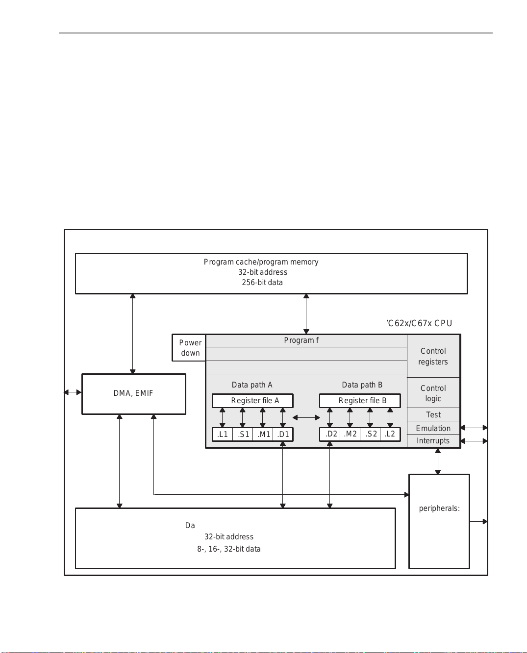
Figure 1–1 is the block diagram for the TMS320C62x/C67x DSPs. The
’C62x/C67x devices come with program memory, which, on some devices,
can be used as a program cache. The devices also have varying sizes of data
memory. Peripherals such as a direct memory access (DMA) controller,
power-down logic, and external memory interface (EMIF) usually come with
the CPU, while peripherals such as serial ports and host ports are on only
certain devices. Check the data sheet for your device to determine the specific
peripheral configurations you have.
Figure 1–1. TMS320C62x/C67x Block Diagram
’C62x/’C67x device
Program cache/program memory
32-bit address
256-bit data
TMS320C62x/C67x Architecture
DMA, EMIF
Power
down
Data path A Data path B
Data cache/data memory
32-bit address
8-, 16-, 32-bit data
Program fetch
Instruction dispatch
Instruction decode
.D1.M1.S1.L1
.D2 .M2 .S2 .L2
’C62x/C67x CPU
Control
registers
Control
Register file BRegister file A
logic
Test
Emulation
Interrupts
Additional
peripherals:
Timers,
serial ports,
etc.
Introduction
1-7
Page 27

TMS320C62x/C67x Architecture
1.4.1 Central Processing Unit (CPU)
The ’C62x/C67x CPU, shaded in Figure 1–1, is common to all the ’C62x/C67x
devices. The CPU contains:
- Program fetch unit
- Instruction dispatch unit
- Instruction decode unit
- Two data paths, each with four functional units
- 32 32-bit registers
- Control registers
- Control logic
- Test, emulation, and interrupt logic
The program fetch, instruction dispatch, and instruction decode units can
deliver up to eight 32-bit instructions to the functional units every CPU clock
cycle. The processing of instructions occurs in each of the two data paths (A
and B), each of which contains four functional units (.L, .S, .M, and .D) and 16
32-bit general-purpose registers. The data paths are described in more detail
in Chapter 2,
means to configure and control various processor operations. To understand
how instructions are fetched, dispatched, decoded, and executed in the data
path, see Chapter 5,
Pipeline
CPU Data Paths and Control
.
. A control register file provides the
TMS320C62x Pipeline
, and Chapter 6,
TMS320C67x
1.4.2 Internal Memory
The ’C62x/C67x have a 32-bit, byte-addressable address space. Internal (onchip) memory is organized in separate data and program spaces. When offchip memory is used, these spaces are unified on most devices to a single
memory space via the external memory interface (EMIF).
The ’C62x/C67x have two 32-bit internal ports to access internal data memory .
The ’C62x/C67x have a single internal port to access internal program
memory, with an instruction-fetch width of 256 bits.
1-8
Page 28

1.4.3 Peripherals
TMS320C62x/C67x Architecture
The following peripheral modules can complement the CPU on the
’C62x/C67x DSPs. Some devices have a subset of these peripherals but may
not have all of them.
- Serial ports
- Timers
- External memory interface (EMIF) that supports synchronous and
asynchronous SRAM and synchronous DRAM
- DMA controller
- Host-port interface
- Power-down logic that can halt CPU activity, peripheral activity, and
phased-locked loop (PLL) activity to reduce power consumption
Introduction
1-9
Page 29

Chapter 2
CPU Data Paths and Control
This chapter focuses on the CPU, providing information about the data paths
and control registers. The two register files and the data crosspaths are
described.
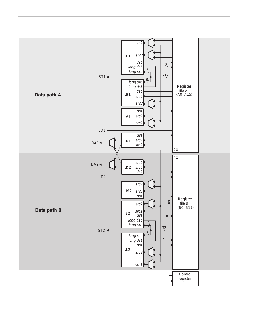
Figure 2–1 and Figure 2–2 show the components of the data paths the ’C62x
and C67x, repectively. These components consist of:
- Two general-purpose register files (A and B)
- Eight functional units (.L1, .L2, .S1, .S2, .M1, .M2, .D1, and .D2)
- Two load-from-memory paths (LD1 and LD2)
- Two store-to-memory paths (ST1 and ST2)
- Two register file cross paths (1X and 2X)
Topic Page
2.1 General-Purpose Register Files 2-4. . . . . . . . . . . . . . . . . . . . . . . . . . . . . . . .
2.2 Functional Units 2-6. . . . . . . . . . . . . . . . . . . . . . . . . . . . . . . . . . . . . . . . . . . . . .
2.3 Register File Cross Paths 2-7. . . . . . . . . . . . . . . . . . . . . . . . . . . . . . . . . . . . . .
2.4 Memory, Load, and Store Paths 2-7. . . . . . . . . . . . . . . . . . . . . . . . . . . . . . . .
2.5 Data Address Paths 2-7. . . . . . . . . . . . . . . . . . . . . . . . . . . . . . . . . . . . . . . . . . .
2.6 TMS320C62x/C67x Control Register File 2-8. . . . . . . . . . . . . . . . . . . . . . . .
2.7 TMS320C67x Extensions to the Control Register File 2-13. . . . . . . . . . .
2-1 August 1996
Page 30
CPU Data Paths and Control
Figure 2–1. TMS320C62x CPU Data Paths
ST1
Data path A
LD1
DA1
DA2
LD2
Data path B
ST2
.L1
long dst
long src
long src
long dst
.S1
.M1
.D1
.D2
.M2
.S2
long dst
long src
long src
long dst
.L2
src1
src2
dst
dst
src1
src2
dst
src1
src2
dst
src1
src2
src2
src1
dst
src2
src1
dst
src2
src1
dst
dst
src2
8
8
32
8
Register
file A
(A0–A15)
2X
1X
Register
file B
(B0–B15)
8
32
8
8
2-2
src1
Control
register
file
Page 31

Figure 2–2. TMS320C67x CPU Data Paths
Á
Á
Á
LD1 32 MSB
ST1
Data path A
LD1 32 LSB
DA1
.L1
long dst
long src
long src
long dst
.S1
.M1
.D1
src1
src2
dst
dst
src1
src2
dst
src1
src2
dst
src1
src2
CPU Data Paths and Control
8
8
8
32
32
8
Register
file A
(A0–A15)
2X
Data path B
DA2
LD2 32 LSB
LD2 32 MSB
ST2
.D2
.M2
.S2
long dst
long src
long src
long dst
.L2
src2
src1
dst
src2
src1
dst
src2
src1
dst
dst
src2
src1
1X
Register
file B
(B0–B15)
8
8
32
8
32
8
Control
register
file
CPU Data Paths and Control
2-3
Page 32

General-Purpose Register Files
2.1 General-Purpose Register Files
There are two general-purpose register files (A and B) in the ’C62x/C67x data
paths. Each of these files contains 16 32-bit registers (A0–A15 for file A and
B0–B15 for file B). The general-purpose registers can be used for data, data
address pointers, or condition registers.
The general-purpose register files support 32- and 40-bit fixed-point data. The
32-bit data can be contained in any general-purpose register. The ’C67x also
supports 32-bit single-precision and 64-bit double-precision data. The 40-bit
data is contained across two registers; the 32 LSBs of the data are placed in
an even register and the remaining eight MSBs are placed in the eight LSBs
of the next upper register (which is always an odd register). There are 16 valid
register pairs for 40-bit data, as shown in Table 2–1. In assembly language
syntax, the register pairs are denoted by a colon between the register names
and the odd register is specified first. The ’C67x also uses these register pairs
to hold 64-bit double-precision floating-point values. See Chapter 4 for more
information on double-precision floating-point values.
Table 2–1. 40-Bit/64-Bit Register Pairs
Register Files
A B
A1:A0 B1:B0
A3:A2 B3:B2
A5:A4 B5:B4
A7:A6 B7:B6
A9:A8 B9:B8
A11:A10 B11:B10
A13:A12 B13:B12
A15:A14
B15:B14
2-4
Page 33

Figure 2–3 illustrates the register storage scheme for 40-bit long data. Operations requiring a long input ignore the 24 MSBs of the odd register. Operations
producing a long result zero-fill the 24 MSBs of the odd register. The even
register is encoded in the opcode.
Figure 2–3. Storage Scheme for 40-Bit Data in a Register Pair
31 0 31 0
Odd register Even register
Ignored
Odd register Even register
Zero-filled
78
Read from registers
39 32 31 0
Write to registers
39 32 31 0
General-Purpose Register Files
40-bit data
40-bit data
CPU Data Paths and Control
2-5
Page 34

Functional Units
2.2 Functional Units
The eight functional units in the ’C62x/C67x data paths can be divided into two
groups of four; each functional unit in one data path is almost identical to the
corresponding unit in the other data path. The functional units are described
in Table 2–2.
Table 2–2. Functional Units and Operations Performed
Functional Unit Fixed-Point Operations Floating-Point Operations
.L unit (.L1,.L2) 32/40-bit arithmetic and compare operations
Leftmost 1 or 0 bit counting for 32 bits
Normalization count for 32 and 40 bits
32-bit logical operations
.S unit (.S1, .S2) 32-bit arithmetic operations
32/40-bit shifts and 32-bit bit-field operations
32-bit logical operations
Branches
Constant generation
Register transfers to/from the control register file
(.S2 only)
.M unit (.M1, .M2) 16 16 bit multiply operations 32 32 bit fixed-point multiply
.D unit (.D1, .D2)
Note: Fixed-point operations are available on both the ’C62x and the ’C67x. Floating-point operations and 32-bit fixed-point
multiply are available only on the ’C67x.
32-bit add, subtract, linear and circular address
calculation
Loads and stores with a 5-bit constant offset
Loads and stores with 15-bit constant offset
(.D2 only)
Arithmetic operations
DP → SP, INT → DP, INT → SP
conversion operations
Compare
Reciprocal and reciprocal squareroot operations
Absolute value operations
SP → DP conversion operations
operations
Floating-point multiply operations
Load doubleword with 5-bit constant
offset
Most data lines in the CPU support 32-bit operands, and some support long
(40-bit) operands. Each functional unit has its own 32-bit write port into a
general-purpose register file. All units ending in 1 (for example, .L1) write to
register file A and all units ending in 2 write to register file B. Each functional
src1
and
src2
unit has two 32-bit read ports for source operands
. Four units
(.L1, .L2, .S1, and .S2) have an extra 8-bit-wide port for 40-bit long writes, as
well as an 8-bit input for 40-bit long reads. Because each unit has its own 32-bit
write port, all eight units can be used in parallel every cycle.
2-6
Page 35

Register File Cross Paths / Memory, Load, and Store Paths / Data Address Paths
2.3 Register File Cross Paths
Each functional unit reads directly from and writes directly to the register file
within its own data path. That is, the .L1, .S1, .D1, and .M1 units write to register
file A and the .L2, .S2, .D2, and .M2 units write to register file B. The register
files are connected to the opposite-side register file’s functional units via the
1X and 2X cross paths. These cross paths allow functional units from one data
path to access a 32-bit operand from the opposite side’s register file. The 1X
cross path allows data path A ’s functional units to read their source from register file B and the 2X cross path allows data path B’s functional units to read their
source from register file A.
Six of the functional units have access to the opposite side’s register file via
a cross path. The .M1, .M2, .S1, and .S2 units’
able between the cross path and the same side register file. The .L1 and .L2
units’
src1
and
path and the same-side register file.
Only two cross paths, 1X and 2X, exist in the ’C62x/C67x CPUs. This limits one
source read from each data path’s opposite register file per cycle, or two crosspath source reads per cycle.
Functional Units
src2
inputs are multiplex-select-
src2
inputs are also multiplex-selectable between the cross
2.4 Memory, Load, and Store Paths
There are two 32-bit paths for loading data from memory to the register file:
LD1 for register file A, and LD2 for register file B. The ’C67x also has a second
32-bit load path for both register files A and B, which allows the LDDW instruction to simultaneously load two 32-bit registers into side A and two 32-bit registers into side B. There are also two 32-bit paths, ST1 and ST2, for storing register values to memory from each register file. The store paths are shared with
the .L and .S long read paths.
2.5 Data Address Paths
The data address paths (DA1 and DA2 in Figure 2–1 and Figure 2–2) coming
out of the .D units allow data addresses generated from one register file to support loads and stores to memory from the other register file.
CPU Data Paths and Control
2-7
Page 36

TMS320C62x/C67x Control Register File
2.6 TMS320C62x/C67x Control Register File
One unit (.S2) can read from and write to the control register file, as shown in
Figure 2–1 and Figure 2–2. Table 2–3 lists the control registers contained in
the control register file and describes each. If more information is available on
a control register, the table lists where to look for that information. Each control
register is accessed by the MVC instruction. See the MVC instruction description in Chapter 3,
TMS320C62x/C67x Fixed-Point Instruction Set
tion on how to use this instruction.
Table 2–3. Control Registers
Register
Abbreviation Name Description Page
, for informa-
AMR Addressing mode register Specifies whether to use linear or circular addres-
sing for each of eight registers; also contains sizes
for circular addressing
CSR Control status register Contains the global interrupt enable bit, cache
control bits, and other miscellaneous control and
status bits
IFR Interrupt flag register Displays status of interrupts 7-14
ISR Interrupt set register Allows you to set pending interrupts manually 7-14
ICR Interrupt clear register Allows you to clear pending interrupts manually 7-14
IER Interrupt enable register Allows enabling/disabling of individual interrupts 7-13
ISTP Interrupt service table pointer Points to the beginning of the interrupt service
table
IRP Interrupt return pointer Contains the address to be used to return from a
maskable interrupt
NRP Nonmaskable interrupt return
pointer
PCE1
Program counter, E1 phase Contains the address of the fetch packet that con-
Contains the address to be used to return from a
nonmaskable interrupt
tains the execute packet in the E1 pipeline stage
2-11
7-16
7-16
2-12
2-9
7-8
2-8
Page 37

2.6.1 Addressing Mode Register (AMR)
For each of the eight registers (A4–A7, B4–B7) that can perform linear or circular addressing, the AMR specifies the addressing mode. A 2-bit field for each
register selects the address modification mode: linear (the default) or circular
mode. With circular addressing, the field also specifies which BK (block size)
field to use for a circular buffer . In addition, the buffer must be aligned on a byte
boundary equal to the block size. The mode select fields and block size fields
are shown in Figure 2–4, and the mode select field encoding is shown in
Table 2–4.
Figure 2–4. Addressing Mode Register (AMR)
TMS320C62x/C67x Control Register File
31 26 1625 21 20
Reserved
R, +0 R, W, +0
Mode select fields
15
B7 mode14B6 mode B5 mode B4 mode A7 mode A6 mode A5 mode A4 mode
Legend: R Readable by the MVC instruction
13 12 11 10 9 8 7 6 5 4 3 2 1 0
W Writeable by the MVC instruction
+0 Value is zero after reset
BK1
R, W, +0
R, W, +0
Block size fields
Table 2–4. Addressing Mode Register (AMR) Mode Select Field Encoding
Mode Description
00 Linear modification
(default at reset)
0 1 Circular addressing using
the BK0 field
1 0 Circular addressing using
the BK1 field
BK0
11
Reserved
The reserved portion of AMR is always 0. The AMR is initialized to 0 at reset.
CPU Data Paths and Control
2-9
Page 38

TMS320C62x/C67x Control Register File
The block size fields, BK0 and BK1, contain 5-bit values used in calculating
block sizes for circular addressing.
Block size (in bytes) = 2
where N is the 5-bit value in BK0 or BK1
Table 2–5 shows block size calculations for all 32 possibilities.
Table 2–5. Block Size Calculations
N Block Size N Block Size
00000 2 10000 131 072
00001 4 10001 262 144
00010 8 10010
00011 16 10011
00100 32 10100
00101 64 10101
00110 128 10110
00111 256 10111
01000 512 11000
01001 1 024 11001
01010 2 048 11010
(N+1)
524 288
1 048 576
2 097 152
4 194 304
8 388 608
16 777 216
33 554 432
67 108 864
134 217 728
2-10
01011 4 096 11011
01100 8 192 11100
01101 16 384 11101
01110 32 768 11110
01111
65 536 11111 4 294 967 296
268 435 456
536 870 912
1 073 741 824
2 147 483 648
Page 39

2.6.2 Control Status Register (CSR)
The CSR, shown in Figure 2–5, contains control and status bits. The functions
of the fields in the CSR are shown in T able 2–6. For the EN, PWRD, PCC, and
DCC fields, see your data sheet to see if your device supports the options that
these fields control and see the
Guide
for more information on these options.
TMS320C6201/C6701 Peripherals Reference
Figure 2–5. Control Status Register (CSR)
31 24
CPU ID
15
PWRD SAT EN PCC DCC
R, W, +0
Legend: R Readable by the MVC instruction
W Writeable by the MVC instruction
+x Value undefined after reset
+0 Value is zero after reset
C Clearable using the MVC instruction
10 9 8 7 5 4 2
R, C, +0
Table 2–6. Control Status Register Field Descriptions
TMS320C62x/C67x Control Register File
Revision ID
R
R, +x
R, W, +0
1
PGIE GIE
1623
0
Bit Position Width Field Name Function
31-24 8 CPU ID CPU ID; defines which CPU.
CPU ID = 00b: indicates ’C62x, CPU ID= 10b: indicates ’C67x
23-16 8 Revision ID Revision ID; defines silicon revision of the CPU
15-10 6 PWRD Control power-down modes; the values are always read as zero.
9 1 SAT The saturate bit, set when any unit performs a saturate, can be
cleared only by the MVC instruction and can be set only by a func-
tional unit. The set by a functional unit has priority over a clear (by
the MVC instruction) if they occur on the same cycle. The saturate
bit is set one full cycle (one delay slot) after a saturate occurs. This
bit will not be modified by a conditional instruction whose condition
is false.
8 1 EN Endian bit: 1 = little endian, 0 = big endian
7-5 3 PCC Program cache control mode
4-2 3 DCC Data cache control mode
†
†
†
1 1 PGIE Previous GIE (global interrupt enable); saves GIE when an inter-
rupt is taken
0 1 GIE Global interrupt enable; enables (1) or disables (0) all interrupts
except the reset interrupt and NMI (nonmaskable interrupt)
†
See the
TMS320C6201/C6701 Peripherals Reference Guide
for more information.
†
CPU Data Paths and Control
2-11
Page 40

TMS320C62x/C67x Control Register File
2.6.3 E1 Phase Program Counter (PCE1)
The PCE1, shown in Figure 2–6, contains the 32-bit address of the execute
packet in the E1 pipeline phase.
Figure 2–6. E1 Phase Program Counter (PCE1)
31
16
PCE1
15
R,W, +x
PCE1
R,W, +x
Legend: R Readable by the MVC instruction
W Writeable by the MVC instruction
+x Value undefined after reset
0
2-12
Page 41

TMS320C67x Extensions to the Control Register File
2.7 TMS320C67x Extensions to the Control Register File
The ’C67x has three additional configuration registers to support floating point
operations. The registers specify the desired floating-point rounding mode for
src1
and
src2
the .L and .M units. They also contain fields to warn if
or denormalized numbers, and if the result overflows, underflows, is inexact,
infinite, or invalid. There are also fields to warn if a divide by 0 was performed,
or if a compare was attempted with a NaN source. Table 2–7 shows the additional registers used by the ’C67x. The OVER, UNDER, INEX, INV AL, DENn,
NANn, INFO, UNORD and DIV0 bits within these registers will not be modified
by a conditional instruction whose condition is false.
Table 2–7. Control Register File Extensions
Register
Abbreviation Name Description Page
are NaN
FADCR Floating-point adder configura-
tion register
FAUCR Floating-point auxiliary configu-
ration register
FMCR Floating-point multiplier config-
uration register
Specifies underflow mode, rounding mode, NaNs,
and other exceptions for the .L unit.
Specifies underflow mode, rounding mode, NaNs,
and other exceptions for the .S unit.
Specifies underflow mode, rounding mode, NaNs,
and other exceptions for the .M unit.
2-14
2-16
2-18
CPU Data Paths and Control
2-13
Page 42

TMS320C67x Extensions to the Control Register File
2.7.1 Floating-Point Adder Configuration Register (FADCR)
The floating-point configuration register (FADCR) contains fields that specify
underflow or overflow, the rounding mode, NaNs, denormalized numbers, and
inexact results for instructions that use the .L functional units. FADCR has a
set of fields specific to each of the .L units, .L1 and .L2. Figure 2–7 shows the
layout of FADCR. The functions of the fields in the FADCR are shown in
Table 2–8.
Figure 2–7. Floating-Point Adder Configuration Register (FADCR)
Fields used by .L2
Fields used by .L1
31
Reserved
R, +0
15
Reserved
R, +0
Legend: R Readable by the MVC instruction
27 26 25
RMode
11 10 9
RMode
W Writeable by the MVC instruction
+0 Value is zero after reset
24 23 22
UNDER
UNDER
INEX OVER INVAL
87 6
INEX OVER INVAL
21 20
INFO
R, W, +0
54
INFO
R, W, +0
19
DEN2
3
DEN2
18
16
17
NAN1
NAN2DEN1
2
NAN2DEN1
0
1
NAN1
2-14
Page 43

TMS320C67x Extensions to the Control Register File
Table 2–8. Floating-Point Adder Configuration Register Field Descriptions
Bit Position Width Field Name Function
31–27 5 Reserved
26–25 2 Rmode .L2 Value 00: Round toward nearest representable floating-point number
V alue 01: Round toward 0 (truncate)
V alue 10: Round toward infinity (round up)
V alue 11: Round toward negative infinity (round down)
24 1 UNDER .L2 Set to 1 when result underflows
23 1 INEX .L2 Set to 1 when result differs from what would have been computed had
the exponent range and precision been unbounded; never set with
INVAL
22 1 OVER .L2 Set to 1 when result overflows
21 1 INFO .L2 Set to 1 when result is signed infinity
20 1 INVAL .L2 Set to 1 when a signed NaN (SNaN) is a source, NaN is a source in
a floating-point to integer conversion, or when infinity is subtracted
from infinity
19 1 DEN2 .L2
18 1 DEN1 .L2
17 1 NAN2 .L2
16 1 NAN1 .L2
15–11 5 Reserved
10–9 2 Rmode .L1 Value 00: Round toward nearest even representable floating-point
8 1 UNDER .L1 Set to 1 when result underflows
7 1 INEX .L1 Set to 1 when result differs from what would have been computed had
6 1 OVER .L1 Set to 1 when result overflows
5 1 INFO .L1 Set to 1 when result is signed infinity
4 1 INVAL .L1 Set to 1 when a signed NaN is a source, NaN is a source in a floating-
3 1 DEN2 .L1
2 1 DEN1 .L1
1 1 NAN2 .L1
0 1 NAN1 .L1
src2
is a denormalized number
src1
is a denormalized number
src2
is NaN
src1
is NaN
number
V alue 01: Round toward 0 (truncate)
V alue 10: Round toward infinity (round up)
V alue 11: Round toward negative infinity (round down)
the exponent range and precision been unbounded; never set with
INVAL
point to integer conversion, or when infinity is subtracted from infinity
src2
is a denormalized number
src1
is a denormalized number
src2
is NaN
src1
is NaN
CPU Data Paths and Control
2-15
Page 44

TMS320C67x Extensions to the Control Register File
2.7.2 Floating-Point Auxiliary Configuration Register (FAUCR)
The floating-point auxiliary register (FAUCR) contains fields that specify underflow or overflow, the rounding mode, NaNs, denormalized numbers, and
inexact results for instructions that use the .S functional units. FAUCR has a
set of fields specific to each of the .S units, .S1 and .S2. Figure 2–8 shows the
layout of FAUCR. The functions of the fields in the FAUCR are shown in
Table 2–9.
Figure 2–8. Floating-Point Auxiliary Configuration Register (FAUCR)
21 20
INFO
R, W, +0
54
INFO
R, W, +0
Fields used by .S2
Fields used by .S1
31
15
27
26 25
Reserved
Reserved
Legend: R Readable by the MVC instruction
DIV0
R, +0
11
10 9
DIV0
UNORD
R, +0
W Writeable by the MVC instruction
+0 Value is zero after reset
24 23 22
UND
INEX OVER INVAL
87 6
UND
INEX OVER INVAL
19
DEN2
3
DEN2
18
16
17
NAN2DEN1UNORD
NAN1
2
NAN2DEN1
0
1
NAN1
2-16
Page 45

TMS320C67x Extensions to the Control Register File
Table 2–9. Floating-Point Auxiliary Configuration Register Field Descriptions
Bit Position Width Field Name Function
31–27 5 Reserved
26 1 DIV0 .S2 Set to 1 when 0 is source to reciprocal operation
25 1 UNORD .S2 Set to 1 when NaN is a source to a compare operation
24 1 UNDER .S2 Set to 1 when result underflows
23 1 INEX .S2 Set to 1 when result differs from what would have been computed had the
exponent range and precision been unbounded; never set with INVAL
22 1 OVER .S2 Set to 1 when result overflows
21 1 INFO .S2 Set to 1 when result is signed infinity
20 1 INVAL .S2 Set to 1 when a signed NaN (SNaN) is a source, NaN is a source in a float-
ing-point to integer conversion, or when infinity is subtracted from infinity
19 1 DEN2 .S2
18 1 DEN1 .S2
17 1 NAN2 .S2
16 1 NAN1 .S2
15–11 5 Reserved
10 1 DIV0 .S1 Set to 1 when 0 is source to reciprocal operation
9 1 UNORD .S1 Set to 1 when NaN is a source to a compare operation
8 1 UNDER .S1 Set to 1 when result underflows
7 1 INEX .S1 Set to 1 when result differs from what would have been computed had the
6 1 OVER .S1 Set to 1 when result overflows
5 1 INFO .S1 Set to 1 when result is signed infinity
4 1 INVAL .S1 Set to 1 when SNaN is a source, NaN is a source in a floating-point to
3 1 DEN2 .S1
2 1 DEN1 .S1
src2
is a denormalized number
src1
is a denormalized number
src2
is NaN
src1
is NaN
exponent range and precision been unbounded; never set with INVAL
integer conversion, or when infinity is subtracted from infinity
src2
is a denormalized number
src1
is a denormalized number
1 1 NAN2 .S1
0 1 NAN1 .S1
src2
src1
is a NaN
is a NaN
CPU Data Paths and Control
2-17
Page 46

TMS320C67x Extensions to the Control Register File
2.7.3 Floating-Point Multiplier Configuration Register (FMCR)
The floating-point multiplier configuration register (FMCR) contains fields that
specify underflow or overflow, the rounding mode, NaNs, denormalized numbers, and inexact results for instructions that use the .M functional units. FMCR
has a set of fields specific to each of the .M units, .M1 and .M2. Figure 2–9
shows the layout of FMCR. The functions of the fields in the FMCR are shown
in Table 2–10.
Figure 2–9. Floating-Point Multiplier Configuration Register (FMCR)
Fields used by .M2
Fields used by .M1
31
Reserved
R, +0
15
Reserved
Legend: R Readable by the MVC instruction
27 26 25
RMode
11 10 9
RMode
R, +0 R, W, +0
W Writeable by the MVC instruction
+0 Value is zero after reset
24 23 22
UNDER
UNDER
INEX OVER
87 6
INEX OVER INVAL
21 20
INVAL
R, W, +0
54
INFO
19
DEN2INFO
3
DEN2
18
16
17
NAN1
NAN2DEN1
2
NAN2DEN1
0
1
NAN1
2-18
Page 47

TMS320C67x Extensions to the Control Register File
Table 2–10. Floating-Point Multiplier Configuration Register Field Descriptions
Bit Position Width Field Name Function
31–27 5 Reserved
26–25 2 Rmode .M2 Value 00: Round toward nearest representable floating-point
number
V alue 01: Round toward 0 (truncate)
V alue 10: Round toward infinity (round up)
V alue 11: Round toward negative infinity (round down)
24 1 UNDER .M2 Set to 1 when result underflows
23 1 INEX .M2 Set to 1 when result differs from what would have been com-
puted had the exponent range and precision been unbounded;
never set with INVAL
22 1 OVER .M2 Set to 1 when result overflows
21 1 INFO .M2 Set to 1 when result is signed infinity
20 1 INVAL .M2 Set to 1 when SNaN is a source, NaN is a source in a floating-
point to integer conversion, or when infinity is subtracted from
infinity
19 1 DEN2 .M2
18 1 DEN1 .M2
17 1 NAN2 .M2
16 1 NAN1 .M2
15–11 5 Reserved
10–9 2 Rmode .M1 Value 00: Round toward nearest representable floating-point
8 1 UNDER .M1 Set to 1 when result underflows
7 1 INEX .M1 Set to 1 when result differs from what would have been com-
6 1 OVER .M1 Set to 1 when result overflows
5 1 INFO .M1 Set to 1 when result is signed infinity
4 1 INVAL .M1 Set to 1 when SNaN is a source, NaN is a source in a floating-
3 1 DEN2 .M1
2 1 DEN1 .M1
1 1 NAN2 .M1
0 1 NAN1 .M1
src2
is a denormalized number
src1
is a denormalized number
src2
is NaN
src1
is NaN
number
V alue 01: Round toward 0 (truncate)
V alue 10: Round toward infinity (round up)
V alue 11: Round toward negative infinity (round down)
puted had the exponent range and precision been unbounded;
never set with INVAL
point to integer conversion, or when infinity is subtracted from
infinity
src2
is a denormalized number
src1
is a denormalized number
src2
is NaN
src1
is NaN
CPU Data Paths and Control
2-19
Page 48

Chapter 3
TMS320C62x/C67x Fixed-Point Instruction Set
The ’C62x and the ’C67x share an instruction set. All of the instructions valid
for the ’C62x are also valid for the ’C67x. However, because the ’C67x is a
floating-point device, there are some instructions that are unique to it and do
not execute on the fixed-point device. This chapter describes the assembly
language instructions that are common to both the ’C62x and ’C67x digital signal processors. Also described are parallel operations, conditional operations,
resource constraints, and addressing modes.
Instructions unique to the ’C67x (floating-point addition, subtraction, multiplication, and others) are described in Chapter 4.
Topic Page
3.1 Instruction Operation and Execution Notations 3-2. . . . . . . . . . . . . . . . . .
3.2 Mapping Between Instructions and Functional Units 3-4. . . . . . . . . . . . .
3.3 TMS320C62x/C67x Opcode Map 3-9. . . . . . . . . . . . . . . . . . . . . . . . . . . . . . . .
3.4 Delay Slots 3-12. . . . . . . . . . . . . . . . . . . . . . . . . . . . . . . . . . . . . . . . . . . . . . . . . .
3.5 Parallel Operations 3-13. . . . . . . . . . . . . . . . . . . . . . . . . . . . . . . . . . . . . . . . . . .
3.6 Conditional Operations 3-16. . . . . . . . . . . . . . . . . . . . . . . . . . . . . . . . . . . . . . .
3.7 Resource Constraints 3-17. . . . . . . . . . . . . . . . . . . . . . . . . . . . . . . . . . . . . . . .
3.8 Addressing Modes 3-21. . . . . . . . . . . . . . . . . . . . . . . . . . . . . . . . . . . . . . . . . . .
3.9 Individual Instruction Descriptions 3-24. . . . . . . . . . . . . . . . . . . . . . . . . . . .
3-1
Page 49

Instruction Operation and Execution Notations
3.1 Instruction Operation and Execution Notations
T able 3–1 explains the symbols used in the fixed-point instruction descriptions.
Table 3–1. Fixed-Point Instruction Operation and Execution Notations
Symbol Meaning
abs(x) Absolute value of x
and Bitwise AND
–a Perform 2s-complement subtraction using the addressing mode de-
fined by the AMR
+a Perform 2s-complement addition using the addressing mode defined
by the AMR
b
y..z
cond Check for either
creg
cstn
int 32-bit integer value
lmb0(x) Leftmost 0 bit search of x
lmb1(x) Leftmost 1 bit search of
long 40-bit integer value
lsbn or LSBn n least significant bits (for example, lsb16)
msbn or MSBn n most significant bits (for example, msb16)
nop No operation
norm(x) Leftmost nonredundant sign bit of x
not Bitwise logical complement
or
op
R Any general-purpose register
scstn n-bit signed constant field
Selection of bits y through z of bit string b
creg
equal to 0 or
3-bit field specifying a conditional register
n-bit constant field (for example, cst5)
x
Bitwise OR
Opfields
creg
not equal to 0
3-2
sint Signed 32-bit integer value
slong Signed 40-bit integer value
slsb16 Signed 16 LSB of register
smsb16
Signed 16 MSB of register
Page 50

Instruction Operation and Execution Notations
Table 3–1. Fixed-Point Instruction Operation and Execution Notations (Continued)
Symbol Meaning
–s Perform 2s-complement subtraction and saturate the result to the re-
sult size if an overflow occurs
+s Perform 2s-complement addition and saturate the result to the result
size if an overflow occurs
ucstn n-bit unsigned constant field (for example, ucst5)
uint Unsigned 32-bit integer value
ulong Unsigned 40-bit integer value
ulsb16 Unsigned 16 LSB of register
umsb16 Unsigned 16 MSB of register
x
clear
x
ext
x
extu
b,e
l,r
l,r
Clear a field in x, specified by b (beginning bit) and e (ending bit)
Extract and sign-extend a field in x, specified by l (shift left value) and
r (shift right value)
Extract an unsigned field in x, specified by l (shift left value) and r (shift
right value)
x
set
b,e
xor Bitwise exclusive OR
xsint Signed 32-bit integer value that can optionally use cross path
xslsb16 Signed 16 LSB of register that can optionally use cross path
xsmsb16 Signed 16 MSB of register that can optionally use cross path
xuint Unsigned 32-bit integer value that can optionally use cross path
xulsb16 Unsigned 16 LSB of register that can optionally use cross path
xumsb16 Unsigned 16 MSB of register that can optionally use cross path
→ Assignment
+ Addition
× Multiplication
– Subtraction
<< Shift left
>>s Shift right with sign extension
>>z
Set field in x to all 1s, specified by b (beginning bit) and e (ending bit)
Shift right with a zero fill
TMS320C62x/C67x Fixed-Point Instruction Set
3-3
Page 51

Mapping Between Instructions and Functional Units
3.2 Mapping Between Instructions and Functional Units
Table 3–2 shows the mapping between instructions and functional units and
Table 3–3 shows the mapping between functional units and instructions.
Table 3–2. Instruction to Functional Unit Mapping
.L Unit .M Unit .S Unit .D Unit
ABS MPY ADD SET ADD STB (15-bit offset)
ADD MPYU ADDK SHL ADDAB STH (15-bit offset)
ADDU MPYUS ADD2 SHR ADDAH STW (15-bit offset)
AND MPYSU AND SHRU ADDAW SUB
‡
‡
‡
CMPEQ MPYH
CMPGT MPYHU
CMPGTU MPYHUS
CMPLT MPYHSU
CMPL TU MPYHL
B disp SSHL LDB SUBAB
†
B IRP
B NRP
†
SUB LDBU SUBAH
SUBU LDH SUBAW
B reg SUB2 LDHU ZERO
CLR XOR LDW
LMBD MPYHLU EXT ZERO LDB (15-bit offset)
MV MPYHULS EXTU LDBU (15-bit offset)
NEG MPYHSLU MV LDH (15-bit offset)
NORM MPYLH MVC
†
LDHU (15-bit offset)
NOT MPYLHU MVK LDW (15-bit offset)
OR MPYLUHS MVKH MV
SADD MPYLSHU MVKLH STB
SAT SMPY NEG STH
SSUB SMPYHL NOT STW
SUB SMPYLH OR
SUBU SMPYH
SUBC
‡
‡
‡
‡
‡
XOR
ZERO
†
S2 only
‡
D2 only
3-4
Page 52

Mapping Between Instructions and Functional Units
Table 3–3. Functional Unit to Instruction Mapping
’C62x/’C67x Functional Units
Instruction .L Unit .M Unit .S Unit .D Unit
ABS
n
ADD
ADDU
ADDAB n
ADDAH n
ADDAW n
ADDK n
ADD2 n
AND n n
B n
B IRP n
B NRP n
B reg n
CLR n
CMPEQ n
CMPGT n
CMPGTU n
n
n
nn
†
†
†
CMPLT n
CMPLTU n
EXT n
EXTU n
IDLE
LDB mem n
LDBU mem n
LDH mem n
LDHU mem n
†
S2 only
‡
D2 only
TMS320C62x/C67x Fixed-Point Instruction Set
3-5
Page 53

Mapping Between Instructions and Functional Units
Table 3–3. Functional Unit to Instruction Mapping (Continued)
’C62x/’C67x Functional Units
Instruction .D Unit.S Unit.M Unit.L Unit
LDW mem n
LDB mem (15-bit offset) n
LDBU mem (15-bit offset) n
LDH mem (15-bit offset) n
LDHU mem (15-bit offset) n
LDW mem (15-bit offset) n
LMBD n
MPY n
MPYU n
MPYUS n
MPYSU n
‡
‡
‡
‡
‡
MPYH n
MPYHU n
MPYHUS n
MPYHSU n
MPYHL n
MPYHLU n
MPYHULS n
MPYHSLU n
MPYLH n
MPYLHU n
MPYLUHS n
MPYLSHU n
MV n n n
†
MVC
n
MVK n
†
S2 only
‡
D2 only
3-6
Page 54

Mapping Between Instructions and Functional Units
Table 3–3. Functional Unit to Instruction Mapping (Continued)
’C62x/’C67x Functional Units
Instruction .D Unit.S Unit.M Unit.L Unit
MVKH n
MVKLH n
NEG
n
n
NOP
NORM n
NOT n n
OR nn
SADD n
SAT n
SET n
SHL n
SHR n
SHRU n
SMPY n
SMPYH n
SMPYHL n
SMPYLH n
SSHL n
SSUB n
STB mem n
STH mem n
STW mem n
STB mem (15-bit offset) n
STH mem (15-bit offset) n
STW mem (15-bit offset) n
SUB n n n
†
S2 only
‡
D2 only
TMS320C62x/C67x Fixed-Point Instruction Set
‡
‡
‡
3-7
Page 55

Mapping Between Instructions and Functional Units
Table 3–3. Functional Unit to Instruction Mapping (Continued)
’C62x/’C67x Functional Units
Instruction .D Unit.S Unit.M Unit.L Unit
SUBU n n
SUBAB n
SUBAH n
SUBAW n
SUBC n
SUB2 n
XOR n n
ZERO n n n
†
S2 only
‡
D2 only
3-8
Page 56

3.3 TMS320C62x/C67x Opcode Map
T able 3–4 and the instruction descriptions in this chapter explain the field syntaxes and values. The ’C62x and ’C67x opcodes are mapped in Figure 3–1.
Table 3–4. TMS320C62x/C67x Opcode Map Symbol Definitions
Symbol Meaning
baseR
base address register
TMS320C62x/C67x Opcode Map
creg
cst
csta
cstb
dst
h
ld/st
mode
offsetR
op
p
r
rsv
s
src2
src1
3-bit field specifying a conditional register
constant
constant a
constant b
destination
MVK or MVKH bit
load/store opfield
addressing mode
register offset
opfield, field within opcode that specifies a unique instruction
parallel execution
LDDW bit
reserved
select side A or B for destination
source 2
source 1
ucstn
x use cross path for
y select .D1 or .D2
z
n-bit unsigned constant field
test for equality with zero or nonzero
TMS320C62x/C67x Fixed-Point Instruction Set
src2
3-9
Page 57

TMS320C62x/C67x Opcode Map
Figure 3–1. TMS320C62x/C67x Opcode Map
Operations on the .L unit
31 29 28 27 23 22 18 17
2 src1/cst
creg z dst
3555 7
Operations on the .M unit
31 29 28 27 23 22 18 17
creg z dst src2
3555 5
Operations on the .D unit
31 29 28 27 23 22 18 17
creg z dst
3555 6
src
2 src1/cst
src
src1 /cst
131211 543210
x
131211 543210
x
1312 543210
op
76
op
76
op
00
10
110
000
000
sp
sp
sp
Load/store with 15-bit offset on the .D unit
31 29 28 27 23 22
creg z dst/src
35 15
Load/store baseR + offsetR/cst on the .D unit
31 29 28 27 23 22 18 17
creg z dst/src
35554 3
Operations on the .S unit
31 29 28 27 23 22 18 17
creg z dst
3555 6
ADDK on the .S unit
31 29 28 27 23 22
baseR offsetR/ucst5
src2
creg z dst
35 16
ucst15
src1/cst
cst
1312 9876 43210
mode r
11
1312 543210
x
78
y
y
op
76 43210
43210
6
ld/st
3
ld/st
6
000
1
5
101
11
01
00
sp
sp
sp
sp
3-10
Page 58

TMS320C62x/C67x Opcode Map
Figure 3–1. TMS320C62x/C67x Opcode Map (Continued)
Field operations (immediate forms) on the .S unit
31 29 28 27 23 22 18 17
creg z dst
355552
MVK and MVKH on the .S unit
31 29 28 27 23 22
src
2
csta cstb op
1312 876543210
0010
76543210
sp
creg
Bcond disp on the .S unit
31 29 28 27
creg z
IDLE
31
NOP
31
z
35 16
dst
cst
321
18 17
161415114 13 12 11 10 9 8 7 6
Reserved
Reserved
14
18 17
16
src
4
13
00000 00 01111
00
00
00
1010
hcst
76543210
0100
0
50
0000
00000
00
sp
sp
1432
sp
0
p
1
TMS320C62x/C67x Fixed-Point Instruction Set
3-11
Page 59

Delay Slots
Á
Á
Á
Á
Á
Á
Á
Á
Á
Á
3.4 Delay Slots
The execution of fixed-point instructions can be defined in terms of delay slots.
The number of delay slots is equivalent to the number of cycles required after
the source operands are read for the result to be available for reading. For a
single-cycle type instruction (such as ADD), source operands read in cycle
produce a result that can be read in cycle i + 1. For a multiply instruction (MPY),
source operands read in cycle i produce a result that can be read in cycle
Table 3–5 shows the number of delay slots associated with each type of instruction.
Delay slots are equivalent to an execution or result latency . All of the instructions that are common to the ’C62x and ’C67x have a functional unit latency
of 1. This means that a new instruction can be started on the functional unit
each cycle. Single-cycle throughput is another term for single-cycle functional
unit latency.
Table 3–5. Delay Slot and Functional Unit Latency Summary
i +
i
2.
Delay
Instruction Type
БББББББББ
NOP (no operation)
Store
Single cycle
БББББББББ
Multiply (16 16)
Load
Branch
†
Cycle i is in the E1 pipeline phase.
‡
The branch to label, branch to IRP, and branch to NRP instructions instruction does not read any registers.
§
The write on cycle i + 4 uses a separate write port from other .D unit instructions.
Slots
0
ÁÁÁ
0
0
1
ÁÁÁ
4
5
Functional
Unit Latency
1
ÁÁ
1
1
1
ÁÁ
1
1
Read
Cycles
ÁÁÁÁÁÁÁÁÁÁÁ
i
i
i
ÁÁÁ
i
‡
i
†
Write
Cycles
i
i
i + 1
ÁÁ
i, i + 4
†
§
Branch
†
Taken
ÁÁÁÁ
i + 5
3-12
Page 60

3.5 Parallel Operations
Parallel Operations
Instructions are always fetched eight at a time. This constitutes a
The basic format of a fetch packet is shown in Figure 3–2. Fetch packets are
aligned on 256-bit (8-word) boundaries.
Figure 3–2. Basic Format of a Fetch Packet
31 0 31 0 31 0 31 0 31 0 31 0 31 0 31 0
pppppppp
LSBs of
the byte
address
Instruction
A
00000
2
Instruction
B
00100
2
Instruction
C
01000
2
Instruction
D
01100
The execution of the individual instructions is partially controlled by a bit in
each instruction, the p-bit. The p-bit (bit 0) determines whether the instruction
executes in parallel with another instruction. The
to right (lower to higher address). If the p-bit of instruction i is 1, then instruction
i
+ 1 is to be executed in parallel with (in the the same cycle as) instruction i.
If the p-bit of instruction i is 0, then instruction i + 1 is executed in the cycle after
instruction i. All instructions executing in parallel constitute an
An execute packet can contain up to eight instructions. Each instruction in an
execute packet must use a different functional unit.
2
Instruction
E
10000
2
Instruction
F
10100
2
fetch packet
Instruction
G
11000
p
-bits are scanned from left
2
Instruction
H
11100
2
execute packet
.
.
An execute packet cannot cross an 8-word boundary . Therefore, the last p-bit
in a fetch packet is always set to 0, and each fetch packet starts a new execute
p
packet. There are three types of
p
-bit patterns result in the following execution sequences for the eight instruc-
-bit patterns for fetch packets. These three
tions:
- Fully serial
- Fully parallel
- Partially serial
Example 3–1 through Example 3–3 illustrate the conversion of a p-bit sequence into a cycle-by-cycle execution stream of instructions.
TMS320C62x/C67x Fixed-Point Instruction Set
3-13
Page 61

Parallel Operations
Example 3–1. Fully Serial p-Bit Pattern in a Fetch Packet
This p-bit pattern:
31 0 31 0 31 0 31 0 31 0 31 0 31 0 31 0
00000000
InstructionAInstructionBInstructionCInstructionDInstructionEInstructionFInstructionGInstruction
H
results in this execution sequence:
Cycle/Execute
Packet
1 A
2B
3C
4D
5E
6F
7G
8 H
Instructions
The eight instructions are executed sequentially.
Example 3–2. Fully Parallel p-Bit Pattern in a Fetch Packet
This p-bit pattern:
31 0 31 0 31 0 31 0
11111110
31 0 31 0 31 0 31 0
InstructionAInstructionBInstructionCInstructionDInstructionEInstructionFInstructionGInstruction
results in this execution sequence:
Cycle/Execute
Packet
1 A B C D E F G H
Instructions
All eight instructions are executed in parallel.
3-14
H
Page 62

Example 3–3. Partially Serial p-Bit Pattern in a Fetch Packet
This p-bit pattern:
Parallel Operations
31 0 31 0 31 0 31 0
0011
InstructionAInstructionBInstructionCInstructionDInstructionEInstructionFInstructionGInstruction
31 0 31 0 31 0 31 0
0110
results in this execution sequence:
Cycle/Execute
Packet
1 A
2 B
3
4
Note: Instructions C, D, and E do not use any of the same functional units, cross paths, or
other data path resources. This is also true for instructions F, G, and H.
CDE
F G H
Instructions
3.5.1 Example Parallel Code
The || characters signify that an instruction is to execute in parallel with the previous instruction. The code for the fetch packet in Example 3–3 would be represented as this:
instruction A
H
instruction B
instruction C
|| instruction D
|| instruction E
instruction F
|| instruction G
|| instruction H
3.5.2 Branching Into the Middle of an Execute Packet
If a branch into the middle of an execute packet occurs, all instructions at lower
addresses are ignored. In Example 3–3, if a branch to the address containing
instruction D occurs, then only D and E execute. Even though instruction C is
in the same execute packet, it is ignored. Instructions A and B are also ignored
because they are in earlier execute packets. If your result depends on executing A,B, or C, the branch to the middle of the execute packet will produce an
erroneous result.
TMS320C62x/C67x Fixed-Point Instruction Set
3-15
Page 63

Conditional Operations
3.6 Conditional Operations
All instructions can be conditional. The condition is controlled by a 3-bit opcode
field (
creg
) that specifies the condition register tested, and a 1-bit field (z) that
specifies a test for zero or nonzero. The four MSBs of every opcode are
and z. The specified condition register is tested at the beginning of the E1 pipeline stage for all instructions. For more information on the pipeline, see Chap-
TMS320C62x Pipeline
ter 5,
the test is for equality with zero. If z = 0, the test is for nonzero. The case of
creg
= 0 and z = 0 is treated as always true to allow instructions to be executed
unconditionally . The
creg
in Table 3–6.
Table 3–6. Registers That Can Be Tested by Conditional Operations
, and Chapter 6,
TMS320C67x Pipeline
field is encoded in the instruction opcode as shown
creg
. If z = 1,
Specified
Conditional
Register
Unconditional 0 0 0 0
Reserved 0 0 0 1
B0 001 z
B1 010 z
B2 011 z
A1 100 z
A2 101 z
Reserved
Note: x can be any value.
Bit
31 30 29 28
1 1 x x
creg z
Conditional instructions are represented in code by using square brackets, [ ],
surrounding the condition register name. The following execute packet contains two ADD instructions in parallel. The first ADD is conditional on B0 being
nonzero. The second ADD is conditional on B0 being zero. The character ! in-
dicates the inverse of the condition.
[B0] ADD .L1 A1,A2,A3
|| [!B0] ADD .L2 B1,B2,B3
3-16
The above instructions are mutually exclusive. This means that only one will
execute. If they are scheduled in parallel, mutually exclusive instructions are
constrained as described in section 3.7. If mutually exclusive instructions
share any resources as described in section 3.7, they cannot be scheduled in
parallel (put in the same execute packet), even though only one will execute.
Page 64

3.7 Resource Constraints
No two instructions within the same execute packet can use the same
resources. Also, no two instructions can write to the same register during the
same cycle. The following sections describe how an instruction can use each
of the resources.
3.7.1 Constraints on Instructions Using the Same Functional Unit
Two instructions using the same functional unit cannot be issued in the same
execute packet.
The following execute packet is invalid:
ADD .S1 A0, A1, A2 ; \ .S1 is used for
|| SHR .S1 A3, 15, A4 ; / both instructions
The following execute packet is valid:
ADD .L1 A0, A1, A2 ; \ Two different functional
|| SHR .S1 A3, 15, A4 ; / units are used
Resource Constraints
3.7.2 Constraints on Cross Paths (1X and 2X)
One unit (either a .S, .L, or .M unit) per data path, per execute packet, can read
a source operand from its opposite register file via the cross paths (1X and 2X).
For example, .S1 can read both of an instruction’s operands from the A register
file, or it can read one operand from the B register file using the 1X cross path
and the other from the A register file. This is denoted by an X following the unit
name in the instruction syntax.
Two instructions using the same cross path between register files cannot be
issued in the same execute packet, because there is only one path from A to
B and one path from B to A.
The following execute packet is invalid:
ADD.L1X A0,B1,A1 ; \ 1X cross path is used
|| MPY.M1X A4,B4,A5 ; / for both instructions
The following execute packet is valid:
ADD.L1X A0,B1,A1 ; \ Instructions use the 1X and
|| MPY.M2X B4,A4,B2 ; / 2X cross paths
The operand will come from a register file opposite of the destination if the x
bit in the instruction field is set (shown in the opcode map located in Figure 3–1
on page 3-10).
TMS320C62x/C67x Fixed-Point Instruction Set
3-17
Page 65

Resource Constraints
3.7.3 Constraints on Loads and Stores
Load/store instructions can use an address pointer from one register file while
loading to or storing from the other register file. Two load/store instructions using a destination/source from the same register file cannot be issued in the
same execute packet. The address register must be on the same side as the
.D unit used.
The following execute packet is invalid:
LDW.D1 *A0,A1 ; \ .D2 unit must use the address
|| LDW.D2 *A2,B2 ; / register from the B register file
The following execute packet is valid:
LDW.D1 *A0,A1 ; \ Address registers from correct
|| LDW.D2 *B0,B2 ; / register files
Two loads and/or stores loading to and/or storing from the same register file
cannot be issued in the same execute packet.
The following execute packet is invalid:
LDW.D1 *A4,A5 ; \ Loading to and storing from the
|| STW.D2 A6,*B4 ; / same register file
The following execute packets are valid:
LDW.D1 *A4,B5 ; \ Loading to, and storing from
|| STW.D2 A6,*B4 ; / different register files
LDW.D1 *A0,B2 ; \ Loading to
|| LDW.D2 *B0,A1 ; / different register files
3.7.4 Constraints on Long (40-Bit) Data
Because the .S and .L units share a read register port for long source operands
and a write register port for long results, only one long result may be issued
per register file in an execute packet. All instructions with a long result on the
.S and .L units have zero delay slots. See section 2.1 on page 2-4 for the order
for long pairs.
The following execute packet is invalid:
ADD.L1 A5:A4,A1,A3:A2 ; \ Two long writes
|| SHL.S1 A8,A9,A7:A6 ; / on A register file
3-18
Page 66

The following execute packet is valid:
ADD.L1 A5:A4,A1,A3:A2 ; \ One long write for
|| SHL.S2 B8,B9,B7:B6 ; / each register file
Because the .L and .S units share their long read port with the store port, operations that read a long value cannot be issued on the .L and/or .S units in
the same execute packet as a store.
The following execute packet is invalid:
ADD .L1 A5:A4,A1,A3:A2 ; \ Long read operation and a
|| STW .D1 A8,*A9 ; / store
The following execute packet is valid:
ADD.L1 A4, A1, A3:A2 ; \ No long read with
|| STW.D1 A8,*A9 ; / with the store
3.7.5 Constraints on Register Reads
More than four reads of the same register cannot occur on the same cycle.
Conditional registers are not included in this count.
Resource Constraints
The following code sequences are invalid:
MPY .M1 A1,A1,A4 ; five reads of register A1
|| ADD .L1 A1,A1,A5
|| SUB .D1 A1,A2,A3
MPY .M1 A1,A1,A4 ; five reads of register A1
|| ADD .L1 A1,A1,A5
|| SUB .D2x A1,B2,B3
This code sequence is valid:
MPY .M1 A1,A1,A4 ; only four reads of A1
|| [A1] ADD .L1 A0,A1,A5
|| SUB .D1 A1,A2,A3
3.7.6 Constraints on Register Writes
Two instructions cannot write to the same register on the same cycle. Two instructions with the same destination can be scheduled in parallel as long as
they do not write to the destination register on the same cycle. For example,
a MPY issued on cycle i followed by an ADD on cycle i + 1 cannot write to the
same register because both instructions write a result on cycle
the following code sequence is invalid unless a branch occurs after the MPY,
causing the ADD not to be issued.
MPY .M1 A0,A1,A2
ADD .L1 A4,A5,A2
i
+ 1. Therefore,
TMS320C62x/C67x Fixed-Point Instruction Set
3-19
Page 67

Resource Constraints
However, this code sequence is valid:
MPY .M1 A0,A1,A2
|| ADD .L1 A4,A5,A2
Figure 3–3 shows different multiple-write conflicts. For example, ADD and
SUB in execute packet L1 write to the same register. This conflict is easily de-
tectable.
MPY in packet L2 and ADD in packet L3 might both write to B2 simultaneously;
however, if a branch instruction causes the execute packet after L2 to be
something other than L3, a conflict would not occur. Thus, the potential conflict
in L2 and L3 might not be detected by the assembler. The instructions in L4
do not constitute a write conflict because they are mutually exclusive. In contrast, because the instructions in L5 may or may not be mutually exclusive, the
assembler cannot determine a conflict. If the pipeline does receive commands
to perform multiple writes to the same register, the result is undefined.
Figure 3–3. Examples of the Detectability of Write Conflicts by the Assembler
L1: ADD.L2 B5,B6,B7 ; \ detectable, conflict
|| SUB.S2 B8,B9,B7 ; /
L2: MPY.M2 B0,B1,B2 ; \ not detectable
L3: ADD.L2 B3,B4,B2 ; /
L4: [!B0] ADD.L2 B5,B6,B7 ; \ detectable, no conflict
|| [B0] SUB.S2 B8,B9,B7 ; /
L5: [!B1] ADD.L2 B5,B6,B7 ; \ not detectable
|| [B0] SUB.S2 B8,B9,B7 ; /
3-20
Page 68

3.8 Addressing Modes
The addressing modes on the ’C62x and ’C67x are linear, circular using BK0,
and circular using BK1. The mode is specified by the addressing mode register, or AMR (defined in Chapter 2).
All registers can perform linear addressing. Only eight registers can perform
circular addressing: A4–A7 are used by the .D1 unit and B4–B7 are used by
the .D2 unit. No other units can perform circular addressing.
LDB(U)/LDH(U)/LDW, STB/STH/STW, ADDAB/ADDAH/ADDAW/ADDAD,
and SUBAB/SUBAH/SUBAW instructions all use the AMR to determine what
type of address calculations are performed for these registers.
3.8.1 Linear Addressing Mode
3.8.1.1 LD/ST Instructions
Addressing Modes
For load and store instructions, linear mode simply shifts the
and to the left by 2, 1, or 0 for word, halfword, or byte access, respectively , and
then performs an add or a subtract to
cified).
3.8.1.2 ADDA/SUBA Instructions
For integer addition and subtraction instructions, linear mode simply shifts the
src1/cst
respectively, and then performs the add or subtract specified.
operand to the left by 2, 1, or 0 for word, halfword, or byte data sizes,
3.8.2 Circular Addressing Mode
The BK0 and BK1 fields in the AMR specify block sizes for circular addressing.
See section 2.6.1, on page 2-9, for more information on the AMR.
3.8.2.1 LD/ST Instructions
After shifting
respectively, an add or subtract is performed with the carry/borrow inhibited
between bits N and N + 1. Bits N + 1 to 31 of
other carries/borrows propagate as usual. If you specify an
than the circular buffer size, 2
cular buffer size (see Example 3–4). The circular buffer size in the AMR is not
scaled; for example, a block size of 4 is 4 bytes, not 4 data size (byte, half-
word, word). So, to perform circular addressing on an array of 8 words, a size
of 32 should be specified, or N = 4. Example 3–4 shows a LDW performed with
register A4 in circular mode and BK0 = 4, so the buffer size is 32 bytes, 16 halfwords, or 8 words. The value put in the AMR for this example is 0004 0001h.
offsetR/cst
offsetR/cst
baseR
to the left by 2, 1, or 0 for LDW, LDH(U) , or LDB(U),
(depending on the operation spe-
baseR
remain unchanged. All
offsetR/cst
(N + 1)
, the effective
offsetR/cst
is modulo the cir-
oper-
greater
TMS320C62x/C67x Fixed-Point Instruction Set
3-21
Page 69

Addressing Modes
Example 3–4. LDW in Circular Mode
LDW .D1 *++A4[9],A1
Before LDW 1 cycle after LDW 5 cycles after LDW
A4
0000 0100h
A1 XXXX XXXXh A1 XXXX XXXXh A1 1234 5678h
mem 104h 1234 5678h mem 104h 1234 5678h mem 104h 1234 5678h
A4 0000 0104h A4 0000 0104h
Note: 9h words is 24h bytes. 24h bytes is 4 bytes beyond the 32-byte (20h) boundary 100h–11Fh; thus, it is wrapped around to
(124h – 20h = 104h).
3.8.2.2 ADDA/SUBA Instructions
After shifting
src1/cst
to the left by 2, 1, or 0 for ADDAW , ADDAH , or ADDAB,
respectively , an add or a subtract is performed with the carry/borrow inhibited
between bits N and N + 1. Bits N + 1 to 31 (inclusive) of
All other carries/borrows propagate as usual. If you specify
(N + 1)
the circular buffer size, 2
, the effective
offsetR/cst
src2
remain unchanged.
src1
greater than
is modulo the circular
buffer size (see Example 3–5). The circular buffer size in the AMR is not
scaled; for example, a block size of 4 is 4 bytes, not 4 data size (byte, half-
word, word). So, to perform circular addressing on an array of 8 words, a size
of 32 should be specified, or N = 4. Example 3–5 shows an ADDAH performed
with register A4 in circular mode and BK0 = 4, so the buffer size is 32 bytes,
16 halfwords, or 8 words. The value put in the AMR for this example is
0004 0001h.
Example 3–5. ADDAH in Circular Mode
ADDAH .D1 A4,A1,A4
Before ADDAH 1 cycle after ADDAH
A4
0000 0100h
A4 0000 0106h
3-22
A1 0000 0013h A1 0000 0013h
Note: 13h halfwords is 26h bytes. 26h bytes is 6 bytes beyond the 32-byte (20h) boundary
100h–1 1Fh; thus, it is wrapped around to (126h – 20h = 106h).
Page 70

3.8.3 Syntax for Load/Store Address Generation
The ’C62x and ’C67x CPUs have a load/store architecture, which means that
the only way to access data in memory is with a load or store instruction.
Table 3–7 shows the syntax of an indirect address to a memory location.
Sometimes a large offset is required for a load/store. In this case you can use
the B14 or B15 register as the base register, and use a 15-bit constant (
as the offset.
Table 3–7. Indirect Address Generation for Load/Store
Addressing Modes
ucst15
)
Preincrement or
No Modification of
Addressing Type
Register indirect *R *++R
Register relative *+R[
Register relative with
15-bit constant offset
Base + index
Address Register
ucst5
]
*–R[
ucst5
]
*+B14/B15[
*+R[
*–R[
ucst15
offsetR
offsetR
]
]
] not supported not supported
Predecrement of
Address Register
*– –R
ucst5
*++R[
*– –R[
ucst5
*++R[
offsetR
*– –R[
offsetR
Postincrement or
Postdecrement of
Address Register
*R++
*R– –
]
]
]
]
*R++[
*R– –[
*R++[
*R– –[
ucst5
ucst5
offsetR
offsetR
]
]
]
]
TMS320C62x/C67x Fixed-Point Instruction Set
3-23
Page 71

Individual Instruction Descriptions
3.9 Individual Instruction Descriptions
This section gives detailed information on the fixed-point instruction set for the
’C62x and ’C67x. Each instruction presents the following information:
- Assembler syntax
- Functional units
- Operands
- Opcode
- Description
- Execution
- Instruction type
- Delay slots
- Functional Unit Latency
- Examples
The ADD instruction is used as an example to familiarize you with the way
each instruction is described. The example describes the kind of information
you will find in each part of the individual instruction description and where to
obtain more information.
3-24
Page 72

Example Instruction
EXAMPLE
Syntax EXAMPLE (.unit)
.unit = .L1, .L2, .S1, .S2, .D1, .D2
src
and
dst
indicate source and destination, respectively . The (.unit) dictates
which functional unit the instruction is mapped to (.L1, .L2, .S1, .S2, .M1, .M2,
.D1, or .D2).
A table is provided for each instruction that gives the opcode map fields, units
the instruction is mapped to, types of operands, and the opcode.
The opcode map, repeated from the summary figure on page 3-10 shows the
various fields that make up each instruction. These fields are described in
Table 3–4 on page 3-9.
There are instructions that can be executed on more than one functional unit.
Table 3–8 shows how this situation is documented for the ADD instruction.
This instruction has three opcode map fields:
seventh row, the operands have the types
and
dst
, respectively . The ordering of these fields implies
where + represents the operation being performed by the ADD. This operation
can be done on .L1 or .L2 (both are specified in the unit column). The s in front
of each operand signifies that
signed values.
src, dst
src1 (scst5
cst5, long,
),
src2 (slong
src1, src2
and
cst5
), and
, and
long
for
+
long ³ long
dst (slong
dst
. In the
src1, src2
) are all
,
,
In the third row,
front of each operand signifies that all operands are unsigned. Any operand
that begins with x can be read from a register file that is different from the
destination register file. The operand comes from the register file opposite the
destination if the x bit in the instruction is set (shown in the opcode map).
src1, src2
, and
dst
are int, int, and long, respectively . The u in
TMS320C62x/C67x Fixed-Point Instruction Set
3-25
Page 73

EXAMPLE
Example Instruction
Table 3–8. Relationships Between Operands, Operand Size, Signed/Unsigned, Functional
Units, and Opfields for Example Instruction (ADD)
Opcode map field used... For operand type... Unit Opfield Mnemonic
src1
src2
dst
src1
src2
dst
src1
src2
dst
src1
src2
dst
src1
src2
dst
src1
src2
dst
src1
src2
dst
sint
xsint
sint
sint
xsint
slong
uint
xuint
ulong
xsint
slong
slong
xuint
ulong
ulong
scst5
xsint
sint
scst5
slong
slong
.L1,
0000011 ADD
.L2
.L1,
0100011 ADD
.L2
.L1,
0101011 ADDU
.L2
.L1,
0100001 ADD
.L2
.L1,
0101001 ADDU
.L2
.L1,
0000010 ADD
.L2
.L1,
0100000 ADD
.L2
3-26
src1
src2
dst
src1
src2
dst
src2
src1
dst
src2
src1
dst
sint
xsint
sint
scst5
xsint
sint
sint
sint
sint
sint
ucst5
sint
.S1,
.S2
.S1,
.S2
.D1,
.D2
.D1,
.D2
000111 ADD
000110 ADD
010000 ADD
010010 ADD
Page 74

Example Instruction
EXAMPLE
Description Instruction execution and its effect on the rest of the processor or memory con-
tents are described. Any constraints on the operands imposed by the processor or the assembler are discussed. The description parallels and supplements the information given by the execution block.
Execution for .L1, .L2 and .S1, .S2 Opcodes
if (cond)
src1 + src2 → dst
else nop
Execution for .D1, .D2 Opcodes
if (cond)
src2 + src1 → dst
else nop
The execution describes the processing that takes place when the instruction
is executed. The symbols are defined in Table 3–1 on page 3-2.
Pipeline This section contains a table that shows the sources read from, the destina-
tions written to, and the functional unit used during each execution cycle of the
instruction.
Instruction Type This section gives the type of instruction. See section 5.2 on page 5-11 for in-
formation about the pipeline execution of this type of instruction.
Delay Slots This section gives the number of delay slots the instruction takes to execute
See section 3.4 on page 3-12 for an explanation of delay slots.
Functional Unit Latency
This section gives the number of cycles that the functional unit is in use during
the execution of the instruction.
Example Examples of instruction execution. If applicable, register and memory values
are given before and after instruction execution.
TMS320C62x/C67x Fixed-Point Instruction Set
3-27
Page 75

ABS
Integer Absolute Value With Saturation
Syntax ABS (.unit)
src2, dst
.unit = .L1, .L2
Opcode map field used... For operand type... Unit Opfield
src2
dst
src2
dst
xsint
sint
slong
slong
.L1, .L2 0011010
.L1, L2 0111000
Opcode
31 29 28 27 23 22 18 17
src2
) →
0 0 0 0 0
dst
creg z dst
3555 7
src2
Description The absolute value of
Execution if (cond) abs(
src2
131211 543210
x
is placed in
dst
op
.
else nop
src2
when
src2
The absolute value of
is an sint is determined as follows:
110
sp
1) If
src2
2) If
src2
3) If
src2
The absolute value of
1) If
src2
2) If
src2
3) If
src2
Pipeline
Pipeline
Stage
Read
Written
Unit in use .L
Instruction Type Single-cycle
Delay Slots 0
3-28
w 0, then
t 0 and
src2 → dst
src2
–231, then –
= –231, then 231 – 1 →
src2
when
w 0, then
t 0 and
= –239, then 2
src2 → dst
src2
–239, then –
E1
src2
dst
39
– 1 →
src2 → dst
dst
src2
is an slong is determined as follows:
src2 → dst
dst
Page 76

Example 1 ABS .L1 A1,A5
Before instruction 1 cycle after instruction
A1
8000 4E3Dh
A5 XXXX XXXXh A5 7FFF B1C3h 2147463619
Example 2 ABS .L1 A1,A5
Before instruction 1 cycle after instruction
A1
3FF6 0010h
A5 XXXX XXXXh A5 3FF6 0010h 1073086480
Integer Absolute V alue W ith Saturation
–2147463619 A1 8000 4E3Dh –2147463619
1073086480 A1 3FF6 0010h 1073086480
ABS
TMS320C62x/C67x Fixed-Point Instruction Set
3-29
Page 77

ADD(U)
Signed or Unsigned Integer Addition Without Saturation
Syntax ADD (.unit)
or
ADDU (.L1 or .L2)
or
ADD (.D1 or .D2)
.unit = .L1, .L2, .S1, .S2
Opcode map field used... For operand type... Unit Opfield
src1
src2
dst
src1
src2
dst
src1
src2
dst
src1
src2
dst
src1
src2
dst
src1, src2, dst
src1, src2, dst
src2, src1, dst
sint
xsint
sint
sint
xsint
slong
uint
xuint
ulong
xsint
slong
slong
xuint
ulong
ulong
.L1, .L2 0000011
.L1, .L2 0100011
.L1, .L2 0101011
.L1, .L2 0100001
.L1, .L2 0101001
3-30
src1
src2
dst
src1
src2
dst
src1
src2
dst
src1
src2
dst
src2
src1
dst
src2
src1
dst
scst5
xsint
sint
scst5
slong
slong
sint
xsint
sint
scst5
xsint
sint
sint
sint
sint
sint
ucst5
sint
.L1, .L2 0000010
.L1, .L2 0100000
.S1, .S2 0001 11
.S1, .S2 000110
.D1, .D2 010000
.D1, .D2 010010
Page 78

Opcode .L unit
Signed or Unsigned Integer Addition Without Saturation
ADD(U)
31 29 28 27 23 22 18 17
creg z dst
3555 7
src2
src1/cst
131211 543210
x
op
Opcode .S unit
31 29 28 27 23 22 18 17
creg z dst
3555 6
src2
src1/cst
11
1312 543210
x
op
Description for .L1, .L2 and .S1, .S2 Opcodes
src2
is added to
src1
. The result is placed in
dst
.
Execution for .L1, .L2 and .S1, .S2 Opcodes
if (cond)
src1 + src2
→
dst
else nop
Opcode .D unit
31 29 28 27 23 22 18 17
creg z dst
src2
src1/cst
1312 543210
op
76
6
1
10
110
000
000
sp
sp
sp
3555 6
Description for .D1, .D2 Opcodes
src1
is added to
src2
. The result is placed in
dst
.
Execution for .D1, .D2 Opcodes
if (cond)
src2 + src1
→
dst
else nop
Pipeline
Pipeline
Stage
Read
Written
Unit in use .L, .S, or .D
E1
src1, src2
dst
Instruction Type Single-cycle
Delay Slots 0
TMS320C62x/C67x Fixed-Point Instruction Set
3-31
Page 79

ADD(U)
Signed or Unsigned Integer Addition Without Saturation
Example 1 ADD .L2X A1,B1,B2
Before instruction 1 cycle after instruction
A1
0000 325Ah
12890 A1 0000 325Ah
B1 FFFF FF12h –238 B1 FFFF FF12h
B2 XXXX XXXXh B2 0000 316Ch 12652
Example 2 ADDU .L1 A1,A2,A5:A4
Before instruction 1 cycle after instruction
A1
0000 325Ah
12890
†
A1 0000 325Ah
A2 FFFF FF12h 4294967058
†
A2 FFFF FF12h
A5:A4 XXXX XXXX A5:A4 0000 0001h 0000 316Ch 4294979948
Example 3 ADDU .L1 A1,A3:A2,A5:A4
Before instruction 1 cycle after instruction
A1
0000 325Ah
12890 A1 0000 325Ah
A3:A2 0000 00FFh FFFF FF12h 1099511627538‡A3:A2 0000 00FFh FFFF FF12h
A5:A4 0000 0000h 0000 0000h 0 A5:A4 0000 0000h 0000 316Ch 12652
†
Unsigned 32-bit integer
‡
Unsigned 40-bit (long) integer
Example 4 ADD .L1 A1,A3:A2,A5:A4
Before instruction 1 cycle after instruction
A1
0000 325Ah 12890 A1 0000 325Ah
A3:A2 0000 00FFh FFFF FF12h –228
A5:A4 0000 0000h 0000 0000h 0
§
Signed 40-bit (long) integer
§
§
A3:A2 0000 00FFh FFFF FF12h
A5:A4 0000 0000h 0000 316Ch 12652
‡
‡
§
Example 5 ADD .L1 –13,A1,A6
Before instruction 1 cycle after instruction
A1
3-32
0000 325Ah
A6 XXXX XXXXh A6 0000 324Dh 12877
12890 A1 0000 325Ah
Page 80

Signed or Unsigned Integer Addition Without Saturation
Example 6 ADD .D1 26,A1,A6
Before instruction 1 cycle after instruction
A1
0000 325Ah
A6 XXXX XXXXh A6 0000 3274h 12916
ADD(U)
12890 A1 0000 325Ah
TMS320C62x/C67x Fixed-Point Instruction Set
3-33
Page 81

ADDAB/ADDAH/ADDAW
Integer Addition Using Addressing Mode
Syntax ADDAB (.unit)
src2, src1, dst
or
ADDAH (.unit)
src2, src1, dst
or
ADDAW (.unit)
src2, src1, dst
.unit = .D1 or .D2
Opcode map field used... For operand type... Unit Opfield
src2
src1
dst
src2
src1
dst
sint
sint
sint
sint
ucst
sint
.D1, .D2 byte: 110000
.D1, .D2 byte: 110010
5
Opcode
31 29 28 27 23 22 18 17
2 src1/cst
creg z dst
3555 6
src
1312 543210
op
76
10
halfword: 1 10100
word: 1 11000
halfword: 1 10110
word: 1 11010
000
sp
Description
src1
is added to
tion defaults to linear mode. However, if
mode can be changed to circular mode by writing the appropriate value to the
AMR (see section 2.6.1).
sizes respectively. Byte, halfword, and word mnemonics are ADDAB,
ADDAH, and ADDAW, respectively. The result is placed in
Execution if (cond)
else nop
Pipeline
Pipeline
stage
Read
Written
Unit in use .D
Instruction Type Single-cycle
Delay Slots 0
3-34
src2
src2
src1, src2
using the addressing mode specified for
src2
is one of A4–A7 or B4–B7, the
src1
is left shifted by 1 or 2 for halfword and word data
+a
src1
→
dst
E1
dst
dst
src2
.
. The addi-
Page 82

Integer Addition Using Addressing Mode
Example 1 ADDAB .D1 A4,A2,A4
Before instruction 1 cycle after instruction
A2
0000 000Bh
A4 0000 0100h A4 0000 0103h
AMR 0002 0001h AMR 0002 0001h
BK0 = 2 → size = 8
A4 in circular addressing mode using BK0
Example 2 ADDAH .D1 A4,A2,A4
Before instruction 1 cycle after instruction
A2
0000 000Bh
A4 0000 0100h A4 0000 0106h
AMR 0002 0001h AMR 0002 0001h
BK0 = 2 → size = 8
A4 in circular addressing mode using BK0
ADDAB/ADDAH/ADDA W
A2 0000 000Bh
A2 0000 000Bh
Example 3 ADDAW .D1 A4,2,A4
Before instruction 1 cycle after instruction
A4
0002 0000h
AMR 0002 0001h AMR 0002 0001h
BK0 = 2 → size = 8
A4 in circular addressing mode using BK0
A4 0002 0000h
TMS320C62x/C67x Fixed-Point Instruction Set
3-35
Page 83

ADDK
Integer Addition Using Signed 16-Bit Constant
Syntax ADDK (.unit)
cst, dst
.unit = .S1 or .S2
Opcode map field used... For operand type... Unit
cst
dst
scst16
uint
.S1, .S2
Opcode
31
29 28 27 23 22 7
→
cst
165
dst
register specified. The result is
dst
creg
z
1
3 11
dst
Description A 16-bit signed constant is added to the
placed in
Execution if (cond)
dst
cst + dst
.
60
10100
else nop
Pipeline
Pipeline
Stage
Read
E1
cst
sp
Written
Unit in use .S
dst
Instruction Type Single-cycle
Delay Slots 0
Example ADDK .S1 15401,A1
Before instruction 1 cycle after instruction
A1
0021 37E1h
3-36
2176993 A1 0021 740Ah 2192394
Page 84

Two 16-Bit Integer Adds on Upper and Lower Register Halves
ADD2
Syntax ADD2 (.unit)
src1, src2, dst
.unit = .S1 or .S2
Opcode map field used... For operand type... Unit
src1
src2
dst
sint
xsint
sint
Opcode
31 29 28 27 23 22 18 17
creg z dst
3555 6
src2
src1
Description The upper and lower halves of the
src2
lower halves of the
operand. Any carry from the lower half add does not
11
1312 543210
x
src1
0 0 0 0 0 1 0 0 0
operand are added to the upper and
affect the upper half add.
Execution if (cond) {
((lsb16(
((msb16(
src1
src1
) + lsb16(
) + msb16(
src2
)) and FFFFh) or
src2
)) << 16) →
}
else nop
6
dst
.S1, .S2
1
sp
Pipeline
Pipeline
Stage
Read
Written
Unit in use .S
Instruction Type Single-cycle
Delay Slots 0
Example
ADD2 .S1X A1,B1,A2
Before instruction 1 cycle after instruction
A1
0021 37E1h
A2 XXXX XXXXh A2 03BB 1C99h 955 7321
B1 039A E4B8h 922 58552 B1 039A E4B8h
E1
src1, src2
dst
33 14305 A1 0021 37E1h
TMS320C62x/C67x Fixed-Point Instruction Set
3-37
Page 85

AND
Bitwise AND
Syntax AND (.unit)
src1, src2, dst
.unit = .L1 or .L2, .S1 or .S2
Opcode map field used... For operand type... Unit Opfield
src1
src2
dst
src1
src2
dst
src1
src2
dst
src1
src2
dst
Opcode
.L unit form:
31 29 28 27 23 22 18 17
creg z dst
src2
uint
xuint
uint
scst5
xuint
uint
uint
xuint
uint
scst5
xuint
uint
src1/cst
.L1, .L2 1111011
.L1, .L2 1111010
.S1, .S2 011111
.S1, .S2 011110
131211 543210
x
op
110
sp
3555 7
.S unit form:
31 29 28 27 23 22 18 17
creg z dst
3555 6
src2
src1/cst
Description A bitwise AND is performed between
scst
The
Execution if (cond)
5 operands are sign extended to 32 bits.
src1
and
src2
→
dst
11
1312 543210
x
src1
and
op
src2
. The result is placed in
else nop
3-38
6
000
1
sp
dst
.
Page 86

Delay Slots 0
Bitwise AND
AND
Pipeline
Pipeline
Stage
Read
Written
Unit in use .L or .S
E1
src1, src2
dst
Instruction Type Single-cycle
Example 1 AND .L1X A1,B1,A2
Before instruction 1 cycle after instruction
A1
F7A1 302Ah
A2 XXXX XXXXh A2 02A0 2020h
B1 02B6 E724h B1 02B6 E724h
Example 2 AND .L1 15,A1,A3
Before instruction 1 cycle after instruction
A1
32E4 6936h
A1 F7A1 302Ah
A1 32E4 6936h
A3 XXXX XXXXh A3 0000 0006h
TMS320C62x/C67x Fixed-Point Instruction Set
3-39
Page 87

B
Branch Using a Displacement
Syntax B (.unit) label
.unit = .S1 or .S2
Opcode map field used... For operand type... Unit
cst scst21
.S1, .S2
Opcode
31
29 28 27 7
creg
z
1
3 11
Description A 21-bit signed constant specified by
cst
21
cst
is shifted left by 2 bits and is added
60
00100
to the address of the first instruction of the fetch packet that contains the
branch instruction. The result is placed in the program fetch counter (PFC).
The assembler/linker automatically computes the correct value for
following formula:
cst
= (label – PCE1) >> 2
If two branches are in the same execute packet and both are taken, behavior
is undefined.
Two conditional branches can be in the same execute packet if one branch
uses a displacement and the other uses a register, IRP, or NRP. As long as only
one branch has a true condition, the code executes in a well-defined way.
cst
sp
by the
Execution if (cond)
else nop
Notes:
1) PCE1 (program counter) represents the address of the first instruction
in the fetch packet in the E1 stage of the pipeline. PFC is the program
fetch counter.
2) The execute packets in the delay slots of a branch cannot be interrupted.
This is true regardless of whether the branch is taken.
3) See section 3.5.2 on page 3-15 for information on branching into the
middle of an execute packet.
3-40
cst
<< 2 + PCE1 → PFC
Page 88

Branch Using a Displacement
B
Pipeline
Pipeline
Stage
Read
Written
Branch
T aken
Unit in use
Instruction Type Branch
Delay Slots 5
T able 3–9 gives the program counter values and actions for the following code
example.
Example
0000 0000 B .S1 LOOP
0000 0004 ADD .L1 A1, A2, A3
0000 0008 || ADD .L2 B1, B2, B3
0000 000C LOOP: MPY .M1X A3, B3, A4
0000 0010 || SUB .D1 A5, A6, A6
0000 0014 MPY .M1 A3, A6, A5
0000 0018 MPY .M1 A6, A7, A8
0000 001C SHR .S1 A4, 15, A4
0000 0020 ADD .D1 A4, A6, A4
E1 PS
.S
T arget Instruction
PW PR DP DC E1
n
Table 3–9. Program Counter Values for Example Branch Using a Displacement
Program Counter
Cycle
Cycle 0 0000 0000h Branch command executes
Cycle 1 0000 0004h
Cycle 2 0000 000Ch
Cycle 3 0000 0014h
Cycle 4 0000 0018h
Cycle 5 0000 001Ch
Cycle 6 0000 000Ch Branch target code executes
Cycle 7
Value
0000 0014h
TMS320C62x/C67x Fixed-Point Instruction Set
Action
(target code fetched)
3-41
Page 89

B
Branch Using a Register
Syntax B (.unit)
src2
.unit = .S2
Opcode map field used... For operand type... Unit
src2
xuint .S2
Opcode
31 29 28 27 23 22 18 17
creg z dst
3555 6
Description
src2
src2
0 0 0 0 0
is placed in the PFC.
11
1312 543210
x
0 0 1 1 0 1 0 0 0
If two branches are in the same execute packet and are both taken, behavior
is undefined.
Two conditional branches can be in the same execute packet if one branch
uses a displacement and the other uses a register, IRP, or NRP. As long as
onlly one branch has a true condition, the code executes in a well-defined way .
src2
Execution if (cond)
→ PFC
else nop
6
1
sp
Notes:
1) This instruction executes on .S2 only. PFC is program fetch counter .
2) The execute packets in the delay slots of a branch cannot be interrupted.
This is true regardless of whether the branch is taken.
Pipeline
Pipeline
Stage
Read
Written
Branch
T aken
Unit in use
Instruction Type Branch
Delay Slots 5
3-42
E1 PS
src2
.S2
T arget Instruction
PW PR DP DC E1
n
Page 90

Branch Using a Register
B
Table 3–10 gives the program counter values and actions for the following
code example. In this example, the B10 register holds the value 1000 000Ch.
Example
B10 1000 000Ch
1000 0000 B .S2 B10
1000 0004 ADD .L1 A1, A2, A3
1000 0008 || ADD .L2 B1, B2, B3
1000 000C MPY .M1X A3, B3, A4
1000 0010 || SUB .D1 A5, A6, A6
1000 0014 MPY .M1 A3, A6, A5
1000 0018 MPY .M1 A6, A7, A8
1000 001C SHR .S1 A4, 15, A4
1000 0020 ADD .D1 A4, A6, A4
Table 3–10. Program Counter Values for Example Branch Using a Register
Program Counter
Cycle
Cycle 0 1000 0000h Branch command executes
Cycle 1 1000 0004h
Cycle 2 1000 000Ch
Cycle 3 1000 0014h
Cycle 4 1000 0018h
Cycle 5 1000 001Ch
Value
Action
(target code fetched)
Cycle 6 1000 000Ch Branch target code executes
Cycle 7
1000 0014h
TMS320C62x/C67x Fixed-Point Instruction Set
3-43
Page 91

B IRP
Branch Using an Interrupt Return Pointer
Syntax B (.unit) IRP
.unit = .S2
Opcode map field used... For operand type... Unit
src2
xsint .S2
Opcode
31 29 28 27 23 22 18 17
creg z dst
3555 6
0 0 1 1 0
0 0 0 0 0
11
1312 543210
x
0 0 0 0 1 1 0 0 0
6
1
sp
Description IRP is placed in the PFC. This instruction also moves PGIE to GIE. PGIE is
unchanged.
If two branches are in the same execute packet and are both taken, behavior
is undefined.
Two conditional branches can be in the same execute packet if one branch
uses a displacement and the other uses a register, IRP, or NRP. As long as only
one branch has a ture condition, the code executes in a well-defined way.
Execution if (cond) IRP
→ PFC
else nop
Notes:
1) This instruction executes on .S2 only. PFC is the program fetch counter .
2) Refer to the chapter on interrupts for more information on IRP , PGIE, and
GIE.
3) The execute packets in the delay slots of a branch cannot be interrupted.
This is true regardless of whether the branch is taken.
Pipeline
Pipeline
Stage
Read IRP
Written
Branch
T aken
Unit in use
Instruction Type Branch
3-44
E1 PS
.S2
T arget Instruction
PW PR DP DC E1
n
Page 92

Branch Using an Interrupt Return Pointer
Delay Slots 5
Table 3–11 gives the program counter values and actions for the following
code example.
Example Given that an interrupt occurred at
0000 1000 IRP = 0000 1000
PC =
0000 0020 B .S2 IRP
0000 0024 ADD .S1 A0, A2, A1
0000 0028 MPY .M1 A1, A0, A1
0000 002C NOP
0000 0030 SHR .S1 A1, 15, A1
0000 0034 ADD .L1 A1, A2, A1
0000 0038 ADD .L2 B1, B2, B3
Table 3–11. Program Counter Values for B IRP
Program Counter
Cycle
Cycle 0 0000 0020 Branch command executes
Value (Hex)
B IRP
Action
(target code fetched)
Cycle 1 0000 0024
Cycle 2 0000 0028
Cycle 3 0000 002C
Cycle 4 0000 0030
Cycle 5 0000 0034
Cycle 6
0000 1000 Branch target code executes
TMS320C62x/C67x Fixed-Point Instruction Set
3-45
Page 93

B NRP
Branch Using NMI Return Pointer
Syntax B (.unit) NRP
.unit = .S2
Opcode map field used... For operand type... Unit
src2
xsint .S2
Opcode
31 29 28 27 23 22 18 17
creg z dst
3555 6
0 0 1 1 1
0 0 0 0 0
11
1312 543210
x
0 0 0 0 1 1 0 0 0
6
1
sp
Description NRP is placed in the PFC. This instruction also sets NMIE. PGIE is unchanged.
If two branches are in the same execute packet and are both taken, behavior
is undefined.
Two conditional branches can be in the same execute packet if one branch
uses a displacement and the other uses a register, IRP, or NRP. As long as only
one branch has a true condition, the code executes in a well-defined way.
Execution if (cond) NRP
→ PFC
else nop
Notes:
1) This instruction executes on .S2 only. PFC is program fetch counter .
2) Refer to the chapter on interrupts for more information on NRP and
NMIE.
3) The execute packets in the delay slots of a branch cannot be interrupted.
This is true regardless of whether the branch is taken.
Pipeline
Pipeline
Stage
Read NRP
Written
Branch
T aken
Unit in use
Instruction Type Branch
3-46
E1 PS
.S2
T arget Instruction
PW PR DP DC E1
n
Page 94

Delay Slots 5
Table 3–12 gives the program counter values and actions for the following
code example.
Example Given that an interrupt occurred at
0000 1000 NRP = 0000 1000
PC =
0000 0020 B .S2 NRP
0000 0024 ADD .S1 A0, A2, A1
0000 0028 MPY .M1 A1, A0, A1
0000 002C NOP
0000 0030 SHR .S1 A1, 15, A1
0000 0034 ADD .L1 A1, A2, A1
0000 0038 ADD .L2 B1, B2, B3
Table 3–12. Program Counter Values for B NRP
Program Counter
Cycle
Cycle 0 0000 0020 Branch command executes
Value (Hex)
Branch Using NMI Return Pointer
Action
(target code fetched)
B NRP
Cycle 1 0000 0024
Cycle 2 0000 0028
Cycle 3 0000 002C
Cycle 4 0000 0030
Cycle 5 0000 0034
Cycle 6
0000 1000 Branch target code executes
TMS320C62x/C67x Fixed-Point Instruction Set
3-47
Page 95

CLR
Clear a Bit Field
Syntax CLR (.unit)
or
CLR (.unit)
.unit = .S1 or .S2
Opcode map field used... For operand type... Unit Opfield
src2
csta
cstb
dst
src2
src1
dst
Opcode
Constant form:
31
29 28 27 7
creg
z
1
3
dst
23 22
5
Register form:
src2, csta, cstb, dst
src2, src1, dst
18 17
src2
5
csta
uint
ucst5
ucst5
uint
xuint
uint
uint
13512 8
.S1, .S2 11
.S1, .S2 111111
65 0
cstb
52
10
00 10
sp
11
31
3-48
creg
3
29 28 27
z
1
dst
23 22
5
src2
5
18 17
src1
13512
11
111011
x
1
6
65 0
10 00
sp
11
Page 96

Clear a Bit Field
CLR
Description The field in
src2
, specified by
may be specified as constants or as the ten LSBs of the
cstb
being bits 0–4 and
in the field and
words,
csta
and
cstb
cstb
csta
signifies the bit location of the MSB in the field. In other
represent the beginning and ending bits, respectively , of
the field to be cleared. The LSB location of
src2
is 31. In the example below,
are valid for the register version of the instruction. If any of the 22 MSBs are
non-zero, the result is invalid.
src2
31 30 29 28 27 26 25 24 23 22 21 20 19 18 17 16 15 14 13 12 11 10 9 8 7 6 5 4 3 2 1 0
dst
31 30 29 28 27 26 25 24 23 22 21 20 19 18 17 16 15 14 13 12 11 10 9 8 7 6 5 4 3 2 1 0
0xxxxxxxx xxxxxxxxxxxxxxx11 111000
0xxxxxxxx xxxxxxxxxxxxxxx00 000000
Execution If the constant form is used:
src2
clear
if (cond)
csta, cstb
else nop
If the register form is used:
csta
and
bits 5–9.
csta
→
cstb
, is cleared to zero.
csta
signifies the bit location of the LSB
src2
is 0 and the MSB location of
is 15 and
dst
cstb
is 23. Only the ten LSBs
cstb
csta
csta
src1
registers, with
and
cstb
if (cond)
else nop
Pipeline
Pipeline
Stage
Read
Written
Unit in use .S
Instruction Type Single-cycle
Delay Slots 0
Example 1
CLR .S1 A1,4,19,A2
Before instruction 1 cycle after instruction
A1
07A4 3F2Ah
A2 XXXX XXXXh A2 07A0 000Ah
src2
clear
src1, src2
src1
E1
dst
TMS320C62x/C67x Fixed-Point Instruction Set
9..5
,
src1
→
4..0
dst
A1 07A4 3F2Ah
3-49
Page 97

CLR
Clear a Bit Field
Example 2 CLR .S2 B1,B3,B2
Before instruction 1 cycle after instruction
B1
03B6 E7D5h
B2 XXXX XXXXh B2 03B0 0001h
B3 0000 0052h B3 0000 0052h
B1 03B6 E7D5h
3-50
Page 98

Integer Compare for Equality
CMPEQ
Syntax CMPEQ (.unit)
src1, src2, dst
.unit = .L1 or .L2
Opcode map field used... For operand type... Unit Opfield
src1
src2
dst
src1
src2
dst
src1
src2
dst
src1
src2
dst
Opcode
31 29 28 27 23 22 18 17
creg z dst
src2
src1/cst
sint
xsint
uint
scst5
xsint
uint
xsint
slong
uint
scst5
slong
uint
131211 543210
x
.L1, .L2 1010011
.L1, .L2 1010010
.L1, .L2 1010001
.L1, .L2 1010000
op
110
sp
3555 7
Description This instruction compares
dst
. Otherwise, 0 is written to
src1
to
dst
src2
.
. If
src1
equals
src2
Execution if (cond) {
if (
src1
==
src2
) 1 →
dst
else 0 →
dst
}
else nop
Pipeline
Pipeline
Stage
Read
Written
Unit in use .L
E1
src1, src2
dst
Instruction Type Single-cycle
Delay Slots 0
TMS320C62x/C67x Fixed-Point Instruction Set
, then 1 is written to
3-51
Page 99

CMPEQ
Integer Compare for Equality
Example 1 CMPEQ .L1X A1,B1,A2
Before instruction 1 cycle after instruction
A1
0000 4B8h
A2 XXXX XXXXh A2 0000 0000h false
B1 0000 4B7h 1207 B1 0000 4B7h
1208 A1 0000 4B8h
Example 2 CMPEQ .L1 Ch,A1,A2
Before instruction 1 cycle after instruction
A1
0000 000Ch
A2 XXXX XXXXh A2 0000 0001h true
12 A1 0000 000Ch
Example 3 CMPEQ .L2X A1,B3:B2,B1
Before instruction 1 cycle after instruction
A1
F23A 3789h
A1 F23A 3789h
B1 XXXX XXXXh B1 0000 0001h true
B3:B2 0000 0FFh F23A 3789h B3:B2 0000 00FFh F23A 3789h
3-52
Page 100

Signed or Unsigned Integer Compare for Greater Than
CMPGT(U)
Syntax CMPGT (.unit)
or
CMPGTU (.unit)
.unit = .L1 or .L2
Opcode map field
used...
src1
src2
dst
src1
src2
dst
src1
src2
dst
src1
src2
dst
src1
src2
dst
src1, src2, dst
src1, src2, dst
For operand
type...
sint
xsint
uint
scst5
xsint
uint
xsint
slong
uint
scst5
slong
uint
uint
xuint
uint
Unit Opfield Mnemonic
.L1, .L2 10001 11 CMPGT
.L1, .L2 1000110 CMPGT
.L1, .L2 1000101 CMPGT
.L1, .L2 1000100 CMPGT
.L1, .L2 1001111 CMPGTU
src1
src2
dst
src1
src2
dst
src1
src2
dst
ucst4
xuint
uint
xuint
ulong
uint
ucst4
ulong
uint
.L1, .L2 1001 110 CMPGTU
.L1, .L2 1001101 CMPGTU
.L1, .L2 1001100 CMPGTU
Opcode
31 29 28 27 23 22 18 17
creg z dst
3555 7
src2
src1/cst
TMS320C62x/C67x Fixed-Point Instruction Set
131211 543210
x
op
110
sp
3-53
 Loading...