

Page 1

Product
Folder
Order
Now
Technical
Documents
Tools &
Software
Support &
Community
TMS320C6745, TMS320C6747
SPRS377F –SEPTEMBER 2008–REVISED JUNE 2014
TMS320C6745, TMS320C6747 Fixed- and Floating-Point Digital Signal Processor
1 TMS320C6745, TMS320C6747 Fixed- and Floating-Point Digital Signal Processor
1.1 Features
1
• Software Support
– TI DSP/BIOS™
– Chip Support Library and DSP Library
• 375- and 456-MHz TMS320C674x VLIW DSP
• C674x Instruction Set Features
– Superset of the C67x+ and C64x+ ISAs
– Up to 3648 MIPS and 2736 MFLOPS C674x
– Byte-Addressable (8-, 16-, 32-, and 64-Bit Data)
– 8-Bit Overflow Protection
– Bit-Field Extract, Set, Clear
– Normalization, Saturation, Bit-Counting
– Compact 16-Bit Instructions
• C674x Two-Level Cache Memory Architecture
– 32KB of L1P Program RAM/Cache
– 32KB of L1D Data RAM/Cache
– 256KB of L2 Unified Mapped RAM/Cache
– Flexible RAM/Cache Partition (L1 and L2)
• Enhanced Direct Memory Access Controller 3
(EDMA3):
– 2 Transfer Controllers
– 32 Independent DMA Channels
– 8 Quick DMA Channels
– Programmable Transfer Burst Size
• TMS320C674x Fixed- and Floating-Point VLIW
DSP Core
– Load-Store Architecture with Nonaligned
Support
– 64 General-Purpose Registers (32-Bit)
– Six ALU (32- and 40-Bit) Functional Units
– Supports 32-Bit Integer, SP (IEEE Single
Precision/32-Bit) and DP (IEEE Double
Precision/64-Bit) Floating Point
– Supports up to Four SP Additions Per Clock,
Four DP Additions Every 2 Clocks
– Supports up to Two Floating-Point (SP or DP)
Reciprocal Approximation (RCPxP) and
Square-Root Reciprocal Approximation
(RSQRxP) Operations Per Cycle
– Two Multiply Functional Units
– Mixed-Precision IEEE Floating Point Multiply
Supported up to:
– 2 SP x SP -> SP Per Clock
– 2 SP x SP -> DP Every Two Clocks
– 2 SP x DP -> DP Every Three Clocks
– 2 DP x DP -> DP Every Four Clocks
– Fixed-Point Multiply Supports Two 32 x 32-Bit
1
• 128KB of RAM Shared Memory (TMS320C6747
• 3.3-V LVCMOS I/Os (Except for USB Interfaces)
• Two External Memory Interfaces:
• Three Configurable 16550-Type UART Modules:
• LCD Controller (TMS320C6747 Only)
• Two Serial Peripheral Interfaces (SPIs) Each with
• Multimedia Card (MMC)/Secure Digital (SD) Card
• Two Master and Slave Inter-Integrated Circuit (I2C
• One Host-Port Interface (HPI) with 16-Bit-Wide
• Programmable Real-Time Unit Subsystem
Multiplies, Four 16 x 16-Bit Multiplies, or
Eight 8 x 8-Bit Multiplies per Clock Cycle, and
Complex Multiples
– Instruction Packing Reduces Code Size
– All Instructions Conditional
– Hardware Support for Modulo Loop
Operation
– Protected Mode Operation
– Exceptions Support for Error Detection and
Program Redirection
Only)
– EMIFA
– NOR (8- or 16-Bit-Wide Data)
– NAND (8- or 16-Bit-Wide Data)
– 16-Bit SDRAM with 128-MB Address Space
(TMS320C6747 Only)
– EMIFB
– 32-Bit or 16-Bit SDRAM with 256-MB
Address Space (TMS320C6747)
– 16-Bit SDRAM with 128-MB Address Space
(TMS320C6745)
– UART0 with Modem Control Signals
– Autoflow Control Signals (CTS, RTS) on UART0
Only
– 16-Byte FIFO
– 16x or 13x Oversampling Option
One Chip Select
Interface with Secure Data I/O (SDIO)
Bus™)
Muxed Address/Data Bus for High Bandwidth
(TMS320C6747 Only)
(PRUSS)
– Two Independent Programmable Realtime Unit
(PRU) Cores
– 32-Bit Load and Store RISC Architecture
– 4KB of Instruction RAM per Core
– 512 Bytes of Data RAM per Core
An IMPORTANT NOTICE at the end of this data sheet addresses availability, warranty, changes, use in safety-critical applications,
intellectual property matters and other important disclaimers. PRODUCTION DATA.
Page 2

TMS320C6745, TMS320C6747
SPRS377F –SEPTEMBER 2008–REVISED JUNE 2014
www.ti.com
– PRUSS can be Disabled via Software to
Save Power
– Standard Power-Management Mechanism
– Clock Gating
– Entire Subsystem Under a Single PSC Clock
Gating Domain
– Dedicated Interrupt Controller
– Dedicated Switched Central Resource
• USB 1.1 OHCI (Host) with Integrated PHY (USB1)
(TMS320C6747 Only)
• USB 2.0 OTG Port with Integrated PHY (USB0)
– USB 2.0 High- and Full-Speed Client
(TMS320C6747)
– USB 2.0 Full-Speed Client (TMS320C6745)
– USB 2.0 High-, Full-, and Low-Speed Host
(TMS320C6747)
– USB 2.0 Full- and Low-Speed Host
(TMS320C6745)
– High-Speed Functionality Available on
TMS320C6747 Device Only
– End Point 0 (Control)
– End Points 1,2,3,4 (Control, Bulk, Interrupt or
ISOC) RX and TX
• Three Multichannel Audio Serial Ports (McASPs):
– TMS320C6747 Supports 3 McASPs
– TMS320C6745 Supports 2 McASPs
– Six Clock Zones and 28 Serial Data Pins
– Supports TDM, I2S, and Similar Formats
– DIT-Capable (McASP2)
– FIFO Buffers for Transmit and Receive
• 10/100 Mbps Ethernet MAC (EMAC):
– IEEE 802.3 Compliant (3.3-V I/O Only)
– RMII Media-Independent Interface
– Management Data I/O (MDIO) Module
• Real-Time Clock with 32-kHz Oscillator and
Separate Power Rail (TMS320C6747 Only)
• One 64-Bit General-Purpose Timer (Configurable
as Two 32-Bit Timers)
• One 64-Bit General-Purpose Watchdog Timer
(Configurable as Two 32-Bit General-Purpose
Timers)
• Three Enhanced Pulse Width Modulators
(eHRPWMs):
– Dedicated 16-Bit Time-Base Counter with
Period and Frequency Control
– 6 Single Edge, 6 Dual Edge Symmetric, or 3
Dual Edge Asymmetric Outputs
– Dead-Band Generation
– PWM Chopping by High-Frequency Carrier
– Trip Zone Input
• Three 32-Bit Enhanced Capture (eCAP) Modules:
– Configurable as 3 Capture Inputs or 3 Auxiliary
Pulse Width Modulator (APWM) Outputs
– Single-Shot Capture of up to Four Event Time-
Stamps
• Two 32-Bit Enhanced Quadrature Encoder Pulse
(eQEP) Modules
• TMS320C6747 Device:
– 256-Ball Pb-Free Plastic Ball Grid Array (PBGA)
[ZKB Suffix], 1.0-mm Ball Pitch
• TMS320C6745 Device:
– 176-pin PowerPAD™ Plastic Quad Flat Pack
[PTP suffix], 0.5-mm Pin Pitch
• Commercial, Industrial, Extended, or Automotive
Temperature
1.2 Applications
• A/V Receivers
• Automotive Amplifiers
• Soundbars
1.3 Description
The TMS320C6745/6747 device is a low-power digital signal processor based on a TMS320C674x DSP
core. It consumes significantly lower power than other members of the TMS320C6000™ platform of
DSPs.
The TMS320C6745/6747 device enables original-equipment manufacturers (OEMs) and original-design
manufacturers (ODMs) to quickly bring to market devices featuring high processing performance .
The TMS320C6745/6747 DSP core uses a two-level cache-based architecture. The Level 1 program
cache (L1P) is a 32-KB direct mapped cache and the Level 1 data cache (L1D) is a 32-KB 2-way setassociative cache. The Level 2 program cache (L2P) consists of a 256-KB memory space that is shared
between program and data space. L2 memory can be configured as mapped memory, cache, or
combinations of the two. Although the DSP L2 is accessible by other hosts in the system, an additional
128KB of RAM shared memory (TMS320C6747 only) is available for use by other hosts without affecting
DSP performance.
2
TMS320C6745, TMS320C6747 Fixed- and Floating-Point Digital Signal
Processor
• Home Theatre Systems
• Professional Audio
• Network Streaming Audio
Copyright © 2008–2014, Texas Instruments Incorporated
Submit Documentation Feedback
Product Folder Links: TMS320C6745 TMS320C6747
Page 3
www.ti.com
The peripheral set includes: a 10/100 Mbps Ethernet MAC (EMAC) with a management data input/output
(MDIO) module; two I2C Bus interfaces; 3 multichannel audio serial ports (McASPs) with 16/9 serializers
and FIFO buffers; two 64-bit general-purpose timers each configurable (one configurable as watchdog); a
configurable 16-bit host-port interface (HPI) [TMS320C6747 only]; up to 8 banks of 16 pins of generalpurpose input/output (GPIO) with programmable interrupt/event generation modes, multiplexed with other
peripherals; 3 UART interfaces (one with both RTS and CTS); three enhanced high-resolution pulse width
modulator (eHRPWM) peripherals; three 32-bit enhanced capture (eCAP) module peripherals which can
be configured as 3 capture inputs or 3 auxiliary pulse width modulator (APWM) outputs; two 32-bit
enhanced quadrature encoded pulse (eQEP) peripherals; and 2 external memory interfaces: an
asynchronous and SDRAM external memory interface (EMIFA) for slower memories or peripherals, and a
higher speed memory interface (EMIFB) for SDRAM.
The Ethernet Media Access Controller (EMAC) provides an efficient interface between the
TMS320C6745/6747 device and the network. The EMAC supports both 10Base-T and 100Base-TX, or 10
Mbps and 100 Mbps in either half- or full-duplex mode. Additionally, an MDIO interface is available for
PHY configuration.
The rich peripheral set provides the ability to control external peripheral devices and communicate with
external processors. For details on each of the peripherals, see the related sections later in this document
and the associated peripheral reference guides.
TMS320C6745, TMS320C6747
SPRS377F –SEPTEMBER 2008–REVISED JUNE 2014
Device Information
PART NUMBER PACKAGE BODY SIZE
TMS320C6745 HLQFP (176) 24.00 mm x 24.00 mm
TMS320C6747 BGA (256) 17.00 mm x 17.00 mm
(1) For more information on these devices, see Section 8, Mechanical Packaging and Orderable
Information.
(1)
Copyright © 2008–2014, Texas Instruments Incorporated
Product Folder Links: TMS320C6745 TMS320C6747
TMS320C6745, TMS320C6747 Fixed- and Floating-Point Digital Signal
Submit Documentation Feedback
Processor
3
Page 4
Switched Central Resource (SCR)
BOOT ROM
256KB L2 RAM
32KB
L1 RAM
32KB
L1 Pgm
AET
C674x
DSP CPU
DSP Subsystem
JTAG Interface
Serial Interfaces
I C
(2)
2
SPI
(2)
UART
(3)
Audio Ports
McASP
w/FIFO
(2)
DMA
Peripherals
External Memory Interfaces
Connectivity
EDMA3
Control Timers
eHRPWM
(3)
eCAP
(3)
eQEP
(2)
(10/100)
EMAC
(RMII)
MDIO
USB2.0
OTG Ctlr
PHY
MMC/SD
(8b)
EMIFA(8b)
NAND/Flash
EMIFB
SDRAM Only
(16b)
GPIO
PRU
Subsystem
System Control
Input
Clock(s)
Power/Sleep
Controller
Memory
Protection
Pin
Multiplexing
PLL/Clock
Generator
w/OSC
GeneralPurpose
Timer
GeneralPurpose
Timer
(Watchdog)
Switched Central Resource (SCR)
BOOT ROM
256KB L2 RAM
32KB
L1 RAM
32KB
L1 Pgm
AET
C674x
DSP CPU
DSP Subsystem
JTAG Interface
Serial Interfaces
I C
(2)
2
SPI
(2)
UART
(3)
Audio Ports
McASP
w/FIFO
(3)
DMA
Peripherals
Display
Internal Memory
LCD
Ctlr
128KB
RAM
External Memory Interfaces
Connectivity
EDMA3
Control Timers
eHRPWM
(3)
eCAP
(3)
eQEP
(2)
(10/100)
EMAC
(RMII)
MDIO
USB1.1
OHCI Ctlr
PHY
USB2.0
OTG Ctlr
PHY
HPI
MMC/SD
(8b)
EMIFA(8b/16B)
NAND/Flash
16b SDRAM
EMIFB
SDRAM Only
(16b/32b)
GPIO
PRU
Subsystem
System Control
Input
Clock(s)
Power/Sleep
Controller
Memory
Protection
Pin
Multiplexing
RTC/
32-kHz
OSC
PLL/Clock
Generator
w/OSC
GeneralPurpose
Timer
GeneralPurpose
Timer
(Watchdog)
TMS320C6745, TMS320C6747
SPRS377F –SEPTEMBER 2008–REVISED JUNE 2014
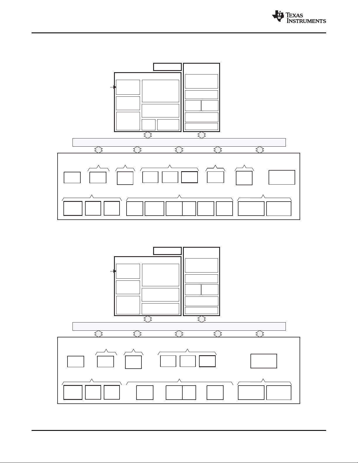
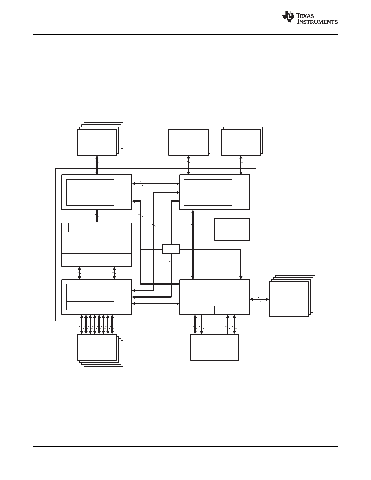
1.4 Functional Block Diagram
www.ti.com
Note: Not all peripherals are available at the same time due to multiplexing. See Table 3-1 for details on which device
components are available on each device.
Figure 1-1. TMS320C6747 Functional Block Diagram
4
Note: Not all peripherals are available at the same time due to multiplexing. See Table 3-1 for details on which device
components are available on each device.
TMS320C6745, TMS320C6747 Fixed- and Floating-Point Digital Signal
Figure 1-2. TMS320C6745 Functional Block Diagram
Processor
Product Folder Links: TMS320C6745 TMS320C6747
Submit Documentation Feedback
Copyright © 2008–2014, Texas Instruments Incorporated
Page 5

www.ti.com
TMS320C6745, TMS320C6747
SPRS377F –SEPTEMBER 2008–REVISED JUNE 2014
Table of Contents
1 TMS320C6745, TMS320C6747 Fixed- and
Floating-Point Digital Signal Processor............. 1
1.1 Features .............................................. 1
1.2 Applications........................................... 2
1.3 Description............................................ 2
1.4 Functional Block Diagram ............................ 4
2 Revision History ......................................... 6
3 Device Overview ......................................... 8
3.1 Device Characteristics................................ 8
3.2 Device Compatibility.................................. 9
3.3 DSP Subsystem..................................... 10
3.4 Memory Map Summary ............................. 21
3.5 Pin Assignments .................................... 26
3.6 Terminal Functions.................................. 28
4 Device Configuration .................................. 56
4.1 Boot Modes ......................................... 56
4.2 SYSCFG Module.................................... 57
4.3 Pullup/Pulldown Resistors .......................... 59
5 Device Operating Conditions ........................ 60
5.1 Absolute Maximum Ratings Over Operating Case
Temperature Range
(Unless Otherwise Noted) ................................. 60
5.2 Handling Ratings .................................... 60
5.3 Recommended Operating Conditions............... 61
5.4 Notes on Recommended Power-On Hours (POH) . 62
5.5 Electrical Characteristics Over Recommended
Ranges of Supply Voltage and Operating Case
Temperature (Unless Otherwise Noted) ............ 63
6 Peripheral Information and Electrical
Specifications........................................... 64
6.1 Parameter Information .............................. 64
6.2 Recommended Clock and Control Signal Transition
Behavior............................................. 65
6.3 Power Supplies...................................... 65
6.4 Reset ................................................ 66
6.5 Crystal Oscillator or External Clock Input........... 69
6.6 Clock PLLs .......................................... 71
6.7 Interrupts ............................................ 75
6.8 General-Purpose Input/Output (GPIO).............. 79
6.9 EDMA ............................................... 82
6.10 External Memory Interface A (EMIFA) .............. 87
6.11 External Memory Interface B (EMIFB) .............. 98
6.12 Memory Protection Units .......................... 106
6.13 MMC / SD / SDIO (MMCSD)....................... 109
6.14 Ethernet Media Access Controller (EMAC) ........ 112
6.15 Management Data Input/Output (MDIO)........... 117
6.16 Multichannel Audio Serial Ports (McASP0, McASP1,
and McASP2) ...................................... 119
6.17 Serial Peripheral Interface Ports (SPI0, SPI1)..... 132
6.18 Enhanced Capture (eCAP) Peripheral............. 151
6.19 Enhanced Quadrature Encoder (eQEP)
Peripheral .......................................... 154
6.20 Enhanced High-Resolution Pulse-Width Modulator
(eHRPWM)......................................... 156
6.21 LCD Controller ..................................... 160
6.22 Timers.............................................. 175
6.23 Inter-Integrated Circuit Serial Ports (I2C0, I2C1) .. 177
6.24 Universal Asynchronous Receiver/Transmitter
(UART)............................................. 182
6.25 USB1 Host Controller Registers (USB1.1 OHCI) .. 184
6.26 USB0 OTG (USB2.0 OTG) ........................ 185
6.27 Host-Port Interface (UHPI)......................... 193
6.28 Power and Sleep Controller (PSC) ................ 200
6.29 Programmable Real-Time Unit Subsystem
(PRUSS) ........................................... 203
6.30 Emulation Logic .................................... 206
6.31 IEEE 1149.1 JTAG ................................ 209
6.32 Real Time Clock (RTC) ............................ 211
7 Device and Documentation Support.............. 214
7.1 Device Support..................................... 214
7.2 Documentation Support............................ 215
7.3 Support Resources ................................ 216
7.4 Related Links ...................................... 216
7.5 Trademarks ........................................ 216
7.6 Electrostatic Discharge Caution ................... 216
7.7 Glossary............................................ 216
8 Mechanical Packaging and Orderable
Information............................................. 217
8.1 Thermal Data for ZKB ............................. 217
8.2 Thermal Data for PTP ............................. 218
8.3 Supplementary Information About the 176-pin PTP
PowerPAD™ Package............................. 218
8.4 Packaging Information ............................. 219
Submit Documentation Feedback
Product Folder Links: TMS320C6745 TMS320C6747
Table of ContentsCopyright © 2008–2014, Texas Instruments Incorporated
5
Page 6
TMS320C6745, TMS320C6747
SPRS377F –SEPTEMBER 2008–REVISED JUNE 2014
2 Revision History
NOTE: Page numbers for previous revisions may differ from page numbers in the current version.
This data manual revision history highlights the changes made to the SPRS377E device-specific data
manual to make it an SPRS377F revision.
Scope: Applicable updates to the TMS320C6747/C6745 Fixed- and Floating-Point Digital Signal
Processor device family, specifically relating to the TMS320C6747 and TMS320C6745 devices, which are
all now in the production data (PD) stage of development, have been incorporated.
SEE ADDITIONS/MODIFICATIONS/DELETIONS
• Turned on Navigation Icons on top of first page.
Global
Section 1.1
Features
Section 1.2
Applications
Section 1.3
Description
Section 3.3.2.3
C674x CPU
Section 3.6
Terminal Functions
Section 3.6.11
Universal
Asynchronous
Receiver/Transmitter
s (UART0, UART1,
UART2)
Section 3.6.21
Reserved and No
Connect
Section 3.6.23
Unused USB0
(USB2.0) and USB1
(USB1.1) Pin
Configurations
Section 5
Device Operating
Conditions
Section 5.4
Notes on
Recommended
Power-On Hours
(POH)
Section 6.10.6
EMIFA Electrical
Data/Timing
• Updated Features, Applications, and Description for consistency and translation.
• Moved Trademarks information from first page to within Section 7, Device and Documentation Support.
• Moved ESDS Warning to within Section 7, Device and Documentation Support.
Deleted Highlights section. Information was duplicated elsewhere in Features.
Added NEW section.
Added NEW Device Information Table.
Table 3-2, C674x Cache Registers:
• Updated/Changed REGISTER DESCRIPTION for BYTE ADDRESSES 0000, 0020, and 0040 from
"...See the System reference Guide..." to "See the Technical Reference Manual..."
Table 3-21, Universal Serial Bus (USB) Terminal Functions:
• Updated/Changed USB0_VDDA12 DESCRIPTION from "...must always be connected via a 1 μF
capacitor..." to "...is recommended to be connected via a 0.22-μF capacitor..."
Table 3-16, Universal Asynchronous Receiver/Transmitter (UART) Terminal Functions:
• Updated/Changed footnote from "...DSP Reference Guide - Literature Number SPRUFK4..." to "...DSP
Technical Reference Manual (SPRUH91)..."
Table 3-26, Reserved and No Connect Terminal Functions:
• Updated/Changed RSV4 DESCRIPTION from "...This pin may be tied high or low." to "...For proper
device operation, this pin must be tied low or to CVDD."
Moved to within Section 3.6, Terminal Functions
Table 3-28, Unused USB0 and USB1 Pin Configurations:
• Updated/Changed USB0_VDDA12 Configuration by combining both Configuration columns and
changing text to "Internal USB0 PHY output connected to an external..."
Section 5.2, Handling Ratings:
• Split handling, ratings, and certifications from the Abs Max table and placed in NEW Handling Ratings
table.
Table 5-1, Recommended Power-On Hours:
• Added Silicon Revision column.
Table 6-22, EMIFA Asynchronous Memory Switching Characteristics:
• Updated/Changed the MIN, NOM, and MAX equations for NO. 3, 10, 15, and 24 from "...(EWC*16)..." to
"...EWC..."
Section 5.3, Recommended Operating Conditions:
• Added "Unless specifically indicated" to "These I/O specifications apply to ..." footnote
www.ti.com
Revision History
6
Revision History Copyright © 2008–2014, Texas Instruments Incorporated
Submit Documentation Feedback
Product Folder Links: TMS320C6745 TMS320C6747
Page 7

www.ti.com
Revision History (continued)
SEE ADDITIONS/MODIFICATIONS/DELETIONS
Table 6-26, EMIFB SDRAM Interface Timing Requirements:
Section 6.11.3
EMIFB Electrical
Data/Timing
Section 6.16
Multichannel Audio
Serial Ports
(McASP0, McASP1,
and McASP2)
Section 7.4
Related Links
Section 7.7
Glossary
• Updated/Changed Parameter No. 19 from "t
• Added new column: "CVDD = 1.3V"
• Added new footnote containing "...range rated devices for 456 MHz max CPU operating..."
• Added new footnote containing "...range rated devices for 400/375/300/266/200 MHz max CPU
operating ..."
Table 6-27, EMIFB SDRAM Interface Switching Characteristics for Commercial (Default) Temperature
Range:
• Updated/Changed table title from "...Switching Characteristics..." to "...Switching Characteristics for
Commercial (Default) Temperature Range"
• Added new footnote containing "...range rated devices for 456 MHz max CPU operating ..."
• Added new footnote containing "...range rated devices for 400/375/300/266/200 MHz max CPU
operating..."
• Updated/Changed CVDD = 1.3V MIN column values for Parameter No. 4, 6, 8, 10, 12, 14, 16, and 18
from "0.9" to "1.1"
• Updated/Changed CVDD = 1.3V MAX column values for Parameter No. 3, 5, 7, 9, 11, 13, 15, and 17
from "5.1" to "4.25"
• Populated CVDD = 1.2V column with values (was empty)
• Updated/Changed Parameter No. 18 from "t
Table 6-28, EMIFB SDRAM Interface Switching Characteristics for Industrial, Extended, and Automotive
Temperature Ranges:
• Added NEW table
Table 6-45, McASP Registers Accessed Through DMA Port:
• Updated/Changed Read Accesses Register Description from "XBUSEL = 0 in XFMT" to "RBUSEL = 0 in
RFMT"
• Updated/Changed Write Accesses Register Description from "RBUSEL = 0 in RFMT" to "XBUSEL = 0 in
XFMT"
Added NEW section.
Added NEW section.
su(DV-CLKH)
ena(CLKH-DLZ)
TMS320C6745, TMS320C6747
SPRS377F –SEPTEMBER 2008–REVISED JUNE 2014
" to "t
" to "t
(DV-CLKH)
"
(CLKH-DLZ)
"
Submit Documentation Feedback
Product Folder Links: TMS320C6745 TMS320C6747
Revision HistoryCopyright © 2008–2014, Texas Instruments Incorporated
7
Page 8
TMS320C6745, TMS320C6747
SPRS377F –SEPTEMBER 2008–REVISED JUNE 2014
3 Device Overview
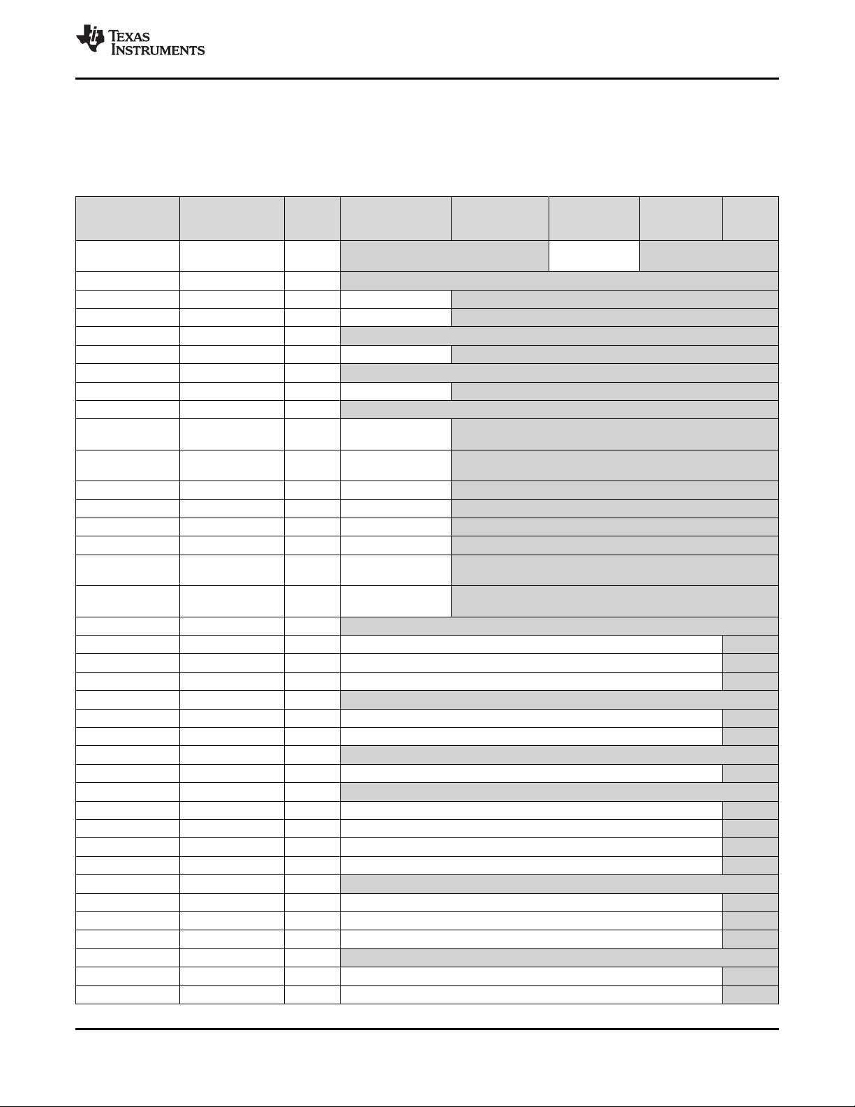
3.1 Device Characteristics
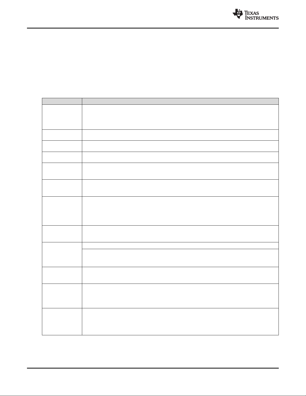
Table 3-1 provides an overview of the C6745/6747 low power digital signal processor. The table shows
significant features of the device, including the capacity of on-chip RAM, peripherals, and the package
type with pin count.
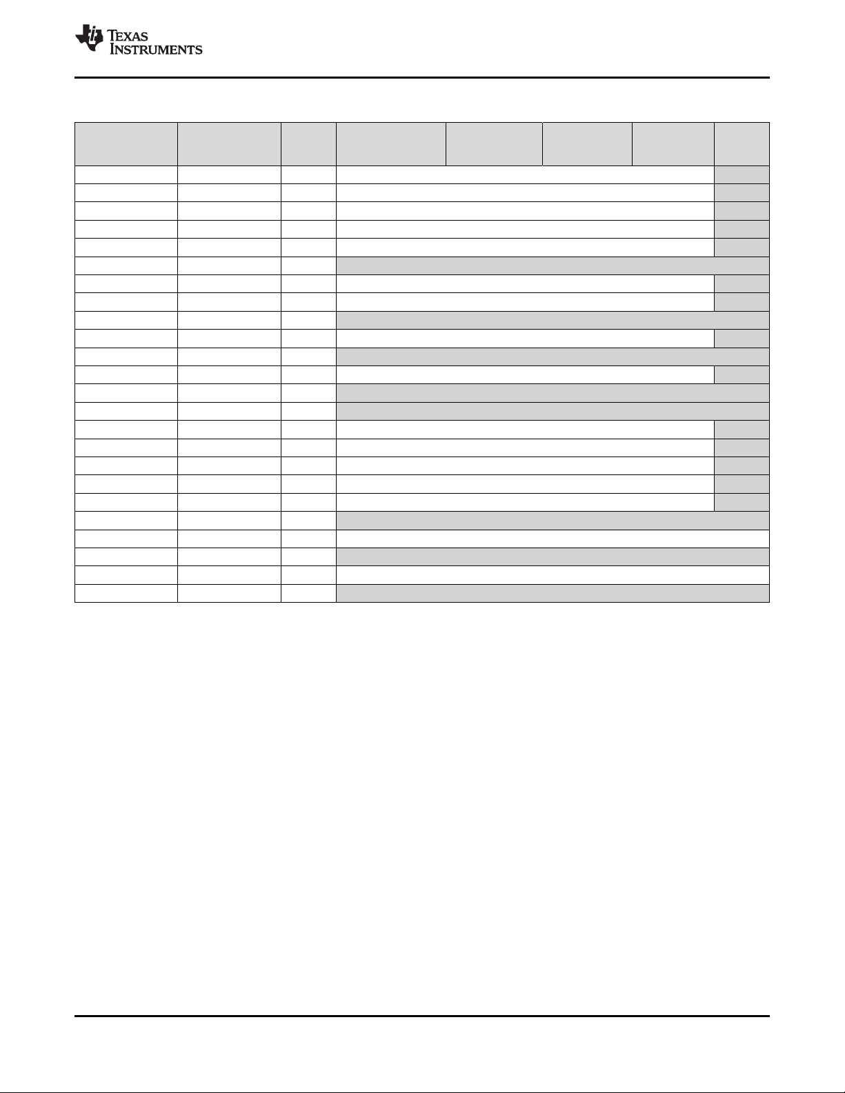
Table 3-1. Characteristics of the C6745/C6747 Processor
HARDWARE FEATURES C6745 C6747
EMIFB 16bit, up to 128MB SDRAM 16/32bit, up to 256MB SDRAM
EMIFA
Flash Card Interface MMC and SD cards supported.
EDMA3 32 independent channels, 8 QDMA channels, 2 Transfer controllers
Timers
UART 3 (one with RTS and CTS flow control)
SPI 2 (each with one hardware chip select)
I2C 2 (both Master/Slave)
Multichannel Audio
Serial Port [McASP]
Peripherals
Not all peripherals pins
are available at the
same time (for more
detail, see the Device
Configurations section).
On-Chip Memory
10/100 Ethernet MAC
with Management Data
I/O
eHRPWM 6 Single Edge, 6 Dual Edge Symmetric, or 3 Dual Edge Asymmetric Outputs
eCAP 3 32-bit capture inputs or 3 32-bit auxiliary PWM outputs
eQEP 2 32-bit QEP channels with 4 inputs/channel
UHPI - 1 (16-bit multiplexed address/data)
USB 2.0 (USB0)
USB 1.1 (USB1) General-Purpose
Input/Output Port
LCD Controller - 1
RTC -
PRU Subsystem
(PRUSS)
Size (Bytes) 320 KB RAM 448 KB RAM
Organization
www.ti.com
Asynchronous (8-bit bus width) RAM,
Flash, NOR, NAND
2 64-Bit General Purpose (each configurable as 2 separate 32-bit timers, 1 configurable
as Watch Dog)
2 (each with transmit/receive, FIFO buffer,
16/9 serializers)
1 (RMII Interface)
Full Speed Host Or Device with On-Chip
PHY
8 banks of 16-bit
2 Programmable PRU Cores
32KB L1 Program (L1P)/Cache (up to 32KB)
32KB L1 Data (L1D)/Cache (up to 32KB)
256KB Unified Mapped RAM/Cache (L2)
DSP Memories can be made accessible to EDMA3, and other peripherals.
Asynchronous (8/16-bit bus width) RAM,
Flash, 16bit up to 128MB SDRAM, NOR,
NAND
3 (each with transmit/receive, FIFO buffer,
16/9 serializers)
High-Speed OTG Controller with on-chip
OTG PHY
Full-Speed OHCI (as host) with on-chip
PHY
1 (32 KHz oscillator and seperate power
trail. Provides time and date tracking and
alarm capability.)
DSP
C674x CPU ID + CPU
Rev ID
C674x Megamodule
Revision
8
Device Overview Copyright © 2008–2014, Texas Instruments Incorporated
Control Status Register
(CSR.[31:16])
Revision ID Register
(MM_REVID[15:0])
Product Folder Links: TMS320C6745 TMS320C6747
-
Submit Documentation Feedback
ADDITIONAL MEMORY
128KB RAM
0x1400
0x0000
Page 9
TMS320C6745, TMS320C6747
www.ti.com
SPRS377F –SEPTEMBER 2008–REVISED JUNE 2014
Table 3-1. Characteristics of the C6745/C6747 Processor (continued)
HARDWARE FEATURES C6745 C6747
JTAG BSDL_ID DEVIDR0 register
CPU Frequency MHz 674x DSP at 375 MHz(1.2V) or 456 MHz (1.3V)
Voltage
Package
Product Status
(1) PRODUCTION DATA information is current as of publication date. Products conform to specifications per the terms of the Texas
Instruments standard warranty. Production processing does not necessarily include testing of all parameters.
(1)
Core (V) 1.2V / 1.3V
I/O (V) 3.3 V
24 mm x 24 mm, 176-Pin, 0.5 mm pitch,
TQFP (PTP)
Product Preview (PP),
Advance Information
(AI),
or Production Data
(PD)
0x0B7D F02F (Silicon Revision 1.0)
0x8B7D F02F (Silicon Revision 1.1)
0x9B7D F02F (Silicon Revisions 3.0, 2.1, and 2.0)
17 mm x 17 mm, 256-Ball 1 mm pitch,
PBGA (ZKB)
375 MHz Versions -PD
456 MHz Version - PD
3.2 Device Compatibility
The C674x DSP core is code-compatible with the C6000™ DSP platform and supports features of both
the C64x+ and C67x+ DSP families.
Submit Documentation Feedback
Product Folder Links: TMS320C6745 TMS320C6747
Device OverviewCopyright © 2008–2014, Texas Instruments Incorporated
9
Page 10
Instruction Fetch
C674x
Fixed/Floating Point CPU
Register
File A
Register
File B
Cache Control
Memory Protect
Bandwidth Mgmt
L1P
256
Cache Control
Memory Protect
Bandwidth Mgmt
L1D
64 64
8 x 32
32K Bytes
L1D RAM/
Cache
32K Bytes
L1P RAM/
Cache
256
Cache Control
Memory Protect
Bandwidth Mgmt
L2
256K Bytes
L2 RAM
256
Boot ROM
256
CFG
MDMA SDMA
EMC
Power Down
Interrupt
Controller
IDMA
256
256
256
256
256
64
High
Performance
Switch Fabric
64
64 64
Configuration
Peripherals
Bus
32
TMS320C6745, TMS320C6747
SPRS377F –SEPTEMBER 2008–REVISED JUNE 2014
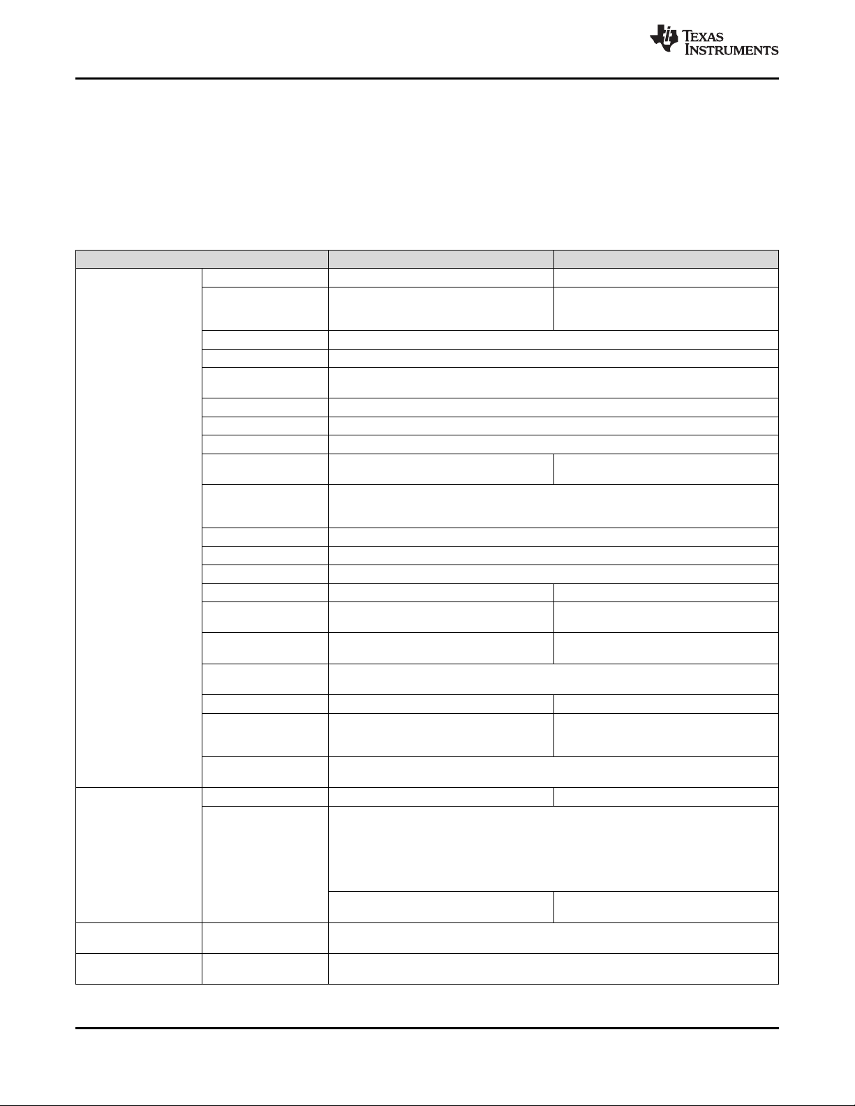
3.3 DSP Subsystem
The DSP Subsystem includes the following features:
• C674x DSP CPU
• 32KB L1 Program (L1P)/Cache (up to 32KB)
• 32KB L1 Data (L1D)/Cache (up to 32KB)
• 256KB Unified Mapped RAM/Cache (L2)
• Boot ROM (cannot be used for application code)
• Little endian
www.ti.com
Figure 3-1. C674x Megamodule Block Diagram
10
Device Overview Copyright © 2008–2014, Texas Instruments Incorporated
Product Folder Links: TMS320C6745 TMS320C6747
Submit Documentation Feedback
Page 11

www.ti.com
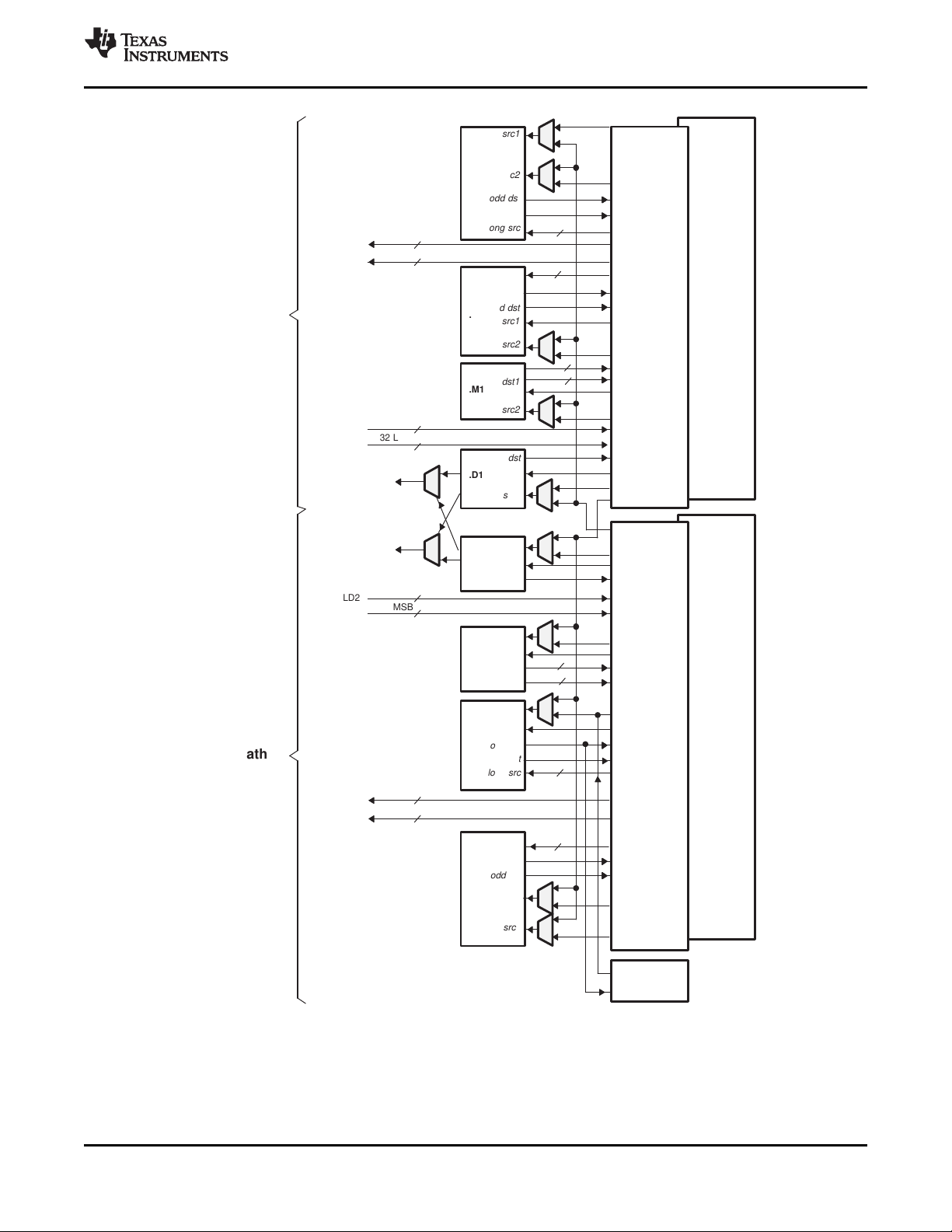
3.3.1 C674x DSP CPU Description
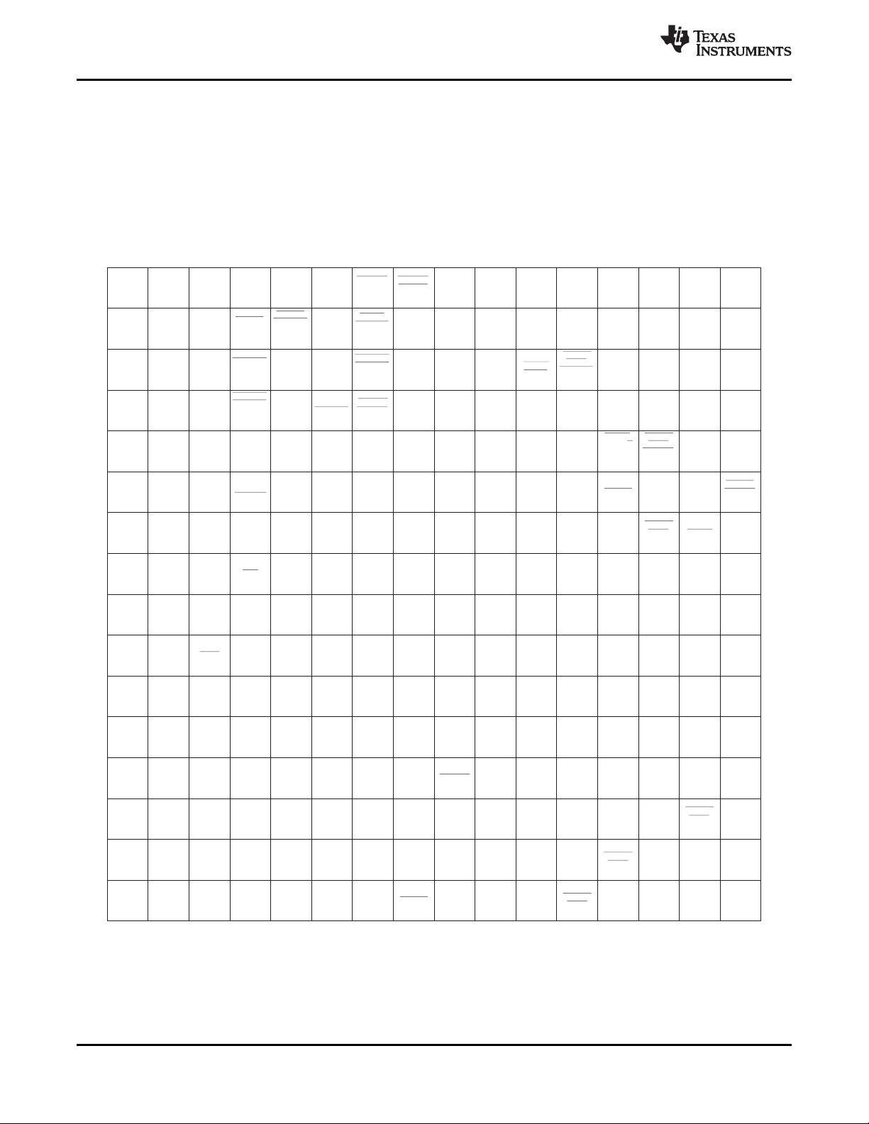
The C674x Central Processing Unit (CPU) consists of eight functional units, two register files, and two
data paths as shown in Figure 3-2. The two general-purpose register files (A and B) each contain 32 32bit registers for a total of 64 registers. The general-purpose registers can be used for data or can be data
address pointers. The data types supported include packed 8-bit data, packed 16-bit data, 32-bit data, 40bit data, and 64-bit data. Values larger than 32 bits, such as 40-bit-long or 64-bit-long values are stored in
register pairs, with the 32 LSBs of data placed in an even register and the remaining 8 or 32 MSBs in the
next upper register (which is always an odd-numbered register).
The eight functional units (.M1, .L1, .D1, .S1, .M2, .L2, .D2, and .S2) are each capable of executing one
instruction every clock cycle. The .M functional units perform all multiply operations. The .S and .L units
perform a general set of arithmetic, logical, and branch functions. The .D units primarily load data from
memory to the register file and store results from the register file into memory.
The C674x CPU combines the performance of the C64x+ core with the floating-point capabilities of the
C67x+ core.
Each C674x .M unit can perform one of the following each clock cycle: one 32 x 32 bit multiply, one 16 x
32 bit multiply, two 16 x 16 bit multiplies, two 16 x 32 bit multiplies, two 16 x 16 bit multiplies with
add/subtract capabilities, four 8 x 8 bit multiplies, four 8 x 8 bit multiplies with add operations, and four
16 x 16 multiplies with add/subtract capabilities (including a complex multiply). There is also support for
Galois field multiplication for 8-bit and 32-bit data. Many communications algorithms such as FFTs and
modems require complex multiplication. The complex multiply (CMPY) instruction takes four 16-bit inputs
and produces a 32-bit real and a 32-bit imaginary output. There are also complex multiplies with rounding
capability that produces one 32-bit packed output that contain 16-bit real and 16-bit imaginary values. The
32 x 32 bit multiply instructions provide the extended precision necessary for high-precision algorithms on
a variety of signed and unsigned 32-bit data types.
TMS320C6745, TMS320C6747
SPRS377F –SEPTEMBER 2008–REVISED JUNE 2014
The .L Unit (or Arithmetic Logic Unit) now incorporates the ability to do parallel add/subtract operations on
a pair of common inputs. Versions of this instruction exist to work on 32-bit data or on pairs of 16-bit data
performing dual 16-bit add and subtracts in parallel. There are also saturated forms of these instructions.
The C674x core enhances the .S unit in several ways. On the previous cores, dual 16-bit MIN2 and MAX2
comparisons were only available on the .L units. On the C674x core they are also available on the .S unit
which increases the performance of algorithms that do searching and sorting. Finally, to increase data
packing and unpacking throughput, the .S unit allows sustained high performance for the quad 8-bit/16-bit
and dual 16-bit instructions. Unpack instructions prepare 8-bit data for parallel 16-bit operations. Pack
instructions return parallel results to output precision including saturation support.
Other new features include:
• SPLOOP - A small instruction buffer in the CPU that aids in creation of software pipelining loops where
multiple iterations of a loop are executed in parallel. The SPLOOP buffer reduces the code size
associated with software pipelining. Furthermore, loops in the SPLOOP buffer are fully interruptible.
• Compact Instructions - The native instruction size for the C6000™ devices is 32 bits. Many common
instructions such as MPY, AND, OR, ADD, and SUB can be expressed as 16 bits if the C674x
compiler can restrict the code to use certain registers in the register file. This compression is
performed by the code generation tools.
• Instruction Set Enhancement - As noted above, there are new instructions such as 32-bit
multiplications, complex multiplications, packing, sorting, bit manipulation, and 32-bit Galois field
multiplication.
• Exceptions Handling - Intended to aid the programmer in isolating bugs. The C674x CPU is able to
detect and respond to exceptions, both from internally detected sources (such as illegal op-codes) and
from system events (such as a watchdog time expiration).
• Privilege - Defines user and supervisor modes of operation, allowing the operating system to give a
basic level of protection to sensitive resources. Local memory is divided into multiple pages, each with
read, write, and execute permissions.
Submit Documentation Feedback
Product Folder Links: TMS320C6745 TMS320C6747
Device OverviewCopyright © 2008–2014, Texas Instruments Incorporated
11
Page 12

TMS320C6745, TMS320C6747
SPRS377F –SEPTEMBER 2008–REVISED JUNE 2014
• Time-Stamp Counter - Primarily targeted for Real-Time Operating System (RTOS) robustness, a freerunning time-stamp counter is implemented in the CPU which is not sensitive to system stalls.
For more details on the C674x CPU and its enhancements over the C64x architecture, see the following
documents:
• TMS320C64x/C64x+ DSP CPU and Instruction Set Reference Guide (SPRU732)
• TMS320C64x Technical Overview (SPRU395)
www.ti.com
12
Device Overview Copyright © 2008–2014, Texas Instruments Incorporated
Submit Documentation Feedback
Product Folder Links: TMS320C6745 TMS320C6747
Page 13
src2
src2
.D1
.M1
.S1
.L1
long src
odd dst
src2
src1
src1
src1
src1
even dst
even dst
odd dst
dst1
dst
src2
src2
src2
long src
DA1
ST1b
LD1b
LD1a
ST1a
Data path A
Odd
register
file A
(A1, A3,
A5...A31)
Odd
register
file B
(B1, B3,
B5...B31)
.D2
src1
dst
src2
DA2
LD2a
LD2b
src2
.M2
src1
dst1
.S2
src1
even dst
long src
odd dst
ST2a
ST2b
long src
.L2
even dst
odd dst
src1
Data path B
Control Register
32 MSB
32 LSB
dst2
(A)
32 MSB
32 LSB
2x
1x
32 LSB
32 MSB
32 LSB
32 MSB
dst2
(B)
(B)
(A)
8
8
8
8
32
32
32
32
(C)
(C)
Even
register
file A
(A0, A2,
A4...A30)
Even
register
file B
(B0, B2,
B4...B30)
(D)
(D)
(D)
(D)
A. On .M unit, dst2 is 32 MSB.
B. On .M unit, dst1 is 32 LSB.
C. On C64x CPU .M unit, src2 is 32 bits; on C64x+ CPU .M unit, src2 is 64 bits.
D. On .L and .S units, odd dst connects to odd register files and even dst connects to even register files.
www.ti.com
TMS320C6745, TMS320C6747
SPRS377F –SEPTEMBER 2008–REVISED JUNE 2014
Figure 3-2. TMS320C674x CPU (DSP Core) Data Paths
Product Folder Links: TMS320C6745 TMS320C6747
Submit Documentation Feedback
Device OverviewCopyright © 2008–2014, Texas Instruments Incorporated
13
Page 14
TMS320C6745, TMS320C6747
SPRS377F –SEPTEMBER 2008–REVISED JUNE 2014
3.3.2 DSP Memory Mapping
The DSP memory map is shown in Section 3.4.
3.3.2.1 External Memories
The DSP has access to the following External memories:
• Asynchronous EMIF / SDRAM / NAND / NOR Flash (EMIFA)
• SDRAM (EMIFB)
3.3.2.2 DSP Internal Memories
The DSP has access to the following DSP memories:
• L2 RAM
• L1P RAM
• L1D RAM
3.3.2.3 C674x CPU
The C674x core uses a two-level cache-based architecture. The Level 1 Program cache (L1P) is 32 KB
direct mapped cache and the Level 1 Data cache (L1D) is 32 KB 2-way set associated cache. The Level 2
memory/cache (L2) consists of a 256 KB memory space that is shared between program and data space.
L2 memory can be configured as mapped memory, cache, or a combination of both.
www.ti.com
Table 3-2 shows a memory map of the C674x CPU cache registers for the device.
Table 3-2. C674x Cache Registers
BYTE ADDRESS ACRONYM REGISTER DESCRIPTION
0x0184 0000 L2CFG
0x0184 0020 L1PCFG
0x0184 0024 L1PCC L1P Freeze Mode Cache configuration register
0x0184 0040 L1DCFG
0x0184 0044 L1DCC L1D Freeze Mode Cache configuration register
0x0184 0048 - 0x0184 0FFC - Reserved
0x0184 1000 EDMAWEIGHT L2 EDMA access control register
0x0184 1004 - 0x0184 1FFC - Reserved
0x0184 2000 L2ALLOC0 L2 allocation register 0
0x0184 2004 L2ALLOC1 L2 allocation register 1
0x0184 2008 L2ALLOC2 L2 allocation register 2
0x0184 200C L2ALLOC3 L2 allocation register 3
0x0184 2010 - 0x0184 3FFF - Reserved
0x0184 4000 L2WBAR L2 writeback base address register
0x0184 4004 L2WWC L2 writeback word count register
0x0184 4010 L2WIBAR L2 writeback invalidate base address register
0x0184 4014 L2WIWC L2 writeback invalidate word count register
0x0184 4018 L2IBAR L2 invalidate base address register
0x0184 401C L2IWC L2 invalidate word count register
0x0184 4020 L1PIBAR L1P invalidate base address register
0x0184 4024 L1PIWC L1P invalidate word count register
0x0184 4030 L1DWIBAR L1D writeback invalidate base address register
0x0184 4034 L1DWIWC L1D writeback invalidate word count register
L2 Cache configuration register (See the Technical Reference Manual
SPRUH91 for the reset configuration)
L1P Size Cache configuration register (See the Technical Reference
Manual SPRUH91 for the reset configuration)
L1D Size Cache configuration register (See the Technical Reference
Manual SPRUH91 for the reset configuration)
14
Device Overview Copyright © 2008–2014, Texas Instruments Incorporated
Submit Documentation Feedback
Product Folder Links: TMS320C6745 TMS320C6747
Page 15
www.ti.com
SPRS377F –SEPTEMBER 2008–REVISED JUNE 2014
Table 3-2. C674x Cache Registers (continued)
BYTE ADDRESS ACRONYM REGISTER DESCRIPTION
0x0184 4038 - Reserved
0x0184 4040 L1DWBAR L1D writeback base address register
0x0184 4044 L1DWWC L1D writeback word count register
0x0184 4048 L1DIBAR L1D invalidate base address register
0x0184 404C L1DIWC L1D invalidate word count register
0x0184 4050 - 0x0184 4FFF - Reserved
0x0184 5000 L2WB L2 writeback all register
0x0184 5004 L2WBINV L2 writeback invalidate all register
0x0184 5008 L2INV L2 Global Invalidate without writeback
0x0184 500C - 0x0184 5027 - Reserved
0x0184 5028 L1PINV L1P Global Invalidate
0x0184 502C - 0x0184 5039 - Reserved
0x0184 5040 L1DWB L1D Global Writeback
0x0184 5044 L1DWBINV L1D Global Writeback with Invalidate
0x0184 5048 L1DINV L1D Global Invalidate without writeback
0x0184 8000 – 0x0184 80FF MAR0 - MAR63 Reserved 0x0000 0000 – 0x3FFF FFFF
0x0184 8100 – 0x0184 817F MAR64 – MAR95
0x0184 8180 – 0x0184 8187 MAR96 - MAR97
0x0184 8188 – 0x0184 818F MAR98 – MAR99
0x0184 8190 – 0x0184 8197 MAR100 – MAR101
0x0184 8198 – 0x0184 819F MAR102 – MAR103
0x0184 81A0 – 0x0184 81FF MAR104 – MAR127 Reserved 0x6800 0000 – 0x7FFF FFFF
0x0184 8200 MAR128
0x0184 8204 – 0x0184 82FF MAR129 – MAR191 Reserved 0x8200 0000 – 0xBFFF FFFF
0x0184 8300 – 0x0184 837F MAR192 – MAR223
0x0184 8380 – 0x0184 83FF MAR224 – MAR255 Reserved 0xE000 0000 – 0xFFFF FFFF
Memory Attribute Registers for EMIFA SDRAM Data (CS0)
0x4000 0000 – 0x5FFF FFFF
Memory Attribute Registers for EMIFA Async Data (CS2)
0x6000 0000 – 0x61FF FFFF
Memory Attribute Registers for EMIFA Async Data (CS3)
0x6200 0000 – 0x63FF FFFF
Memory Attribute Registers for EMIFA Async Data (CS4)
0x6400 0000 – 0x65FF FFFF
Memory Attribute Registers for EMIFA Async Data (CS5)
0x6600 0000 – 0x67FF FFFF
Memory Attribute Register for Shared RAM 0x8000 0000 – 0x8001 FFFF
Reserved 0x8002 0000 – 0x81FF FFFF
Memory Attribute Registers for EMIFB SDRAM Data (CS0)
0xC000 0000 – 0xDFFF FFFF
TMS320C6745, TMS320C6747
Table 3-3. C674x L1/L2 Memory Protection Registers
BYTE ADDRESS ACRONYM REGISTER DESCRIPTION
0x0184 A000 L2MPFAR L2 memory protection fault address register
0x0184 A004 L2MPFSR L2 memory protection fault status register
0x0184 A008 L2MPFCR L2 memory protection fault command register
0x0184 A00C - 0x0184 A0FF - Reserved
0x0184 A100 L2MPLK0 L2 memory protection lock key bits [31:0]
0x0184 A104 L2MPLK1 L2 memory protection lock key bits [63:32]
0x0184 A108 L2MPLK2 L2 memory protection lock key bits [95:64]
0x0184 A10C L2MPLK3 L2 memory protection lock key bits [127:96]
0x0184 A110 L2MPLKCMD L2 memory protection lock key command register
0x0184 A114 L2MPLKSTAT L2 memory protection lock key status register
0x0184 A118 - 0x0184 A1FF - Reserved
0x0184 A200 L2MPPA0
Submit Documentation Feedback
Product Folder Links: TMS320C6745 TMS320C6747
L2 memory protection page attribute register 0
(controls memory address 0x0080 0000 - 0x0080 1FFF)
Device OverviewCopyright © 2008–2014, Texas Instruments Incorporated
15
Page 16

TMS320C6745, TMS320C6747
SPRS377F –SEPTEMBER 2008–REVISED JUNE 2014
Table 3-3. C674x L1/L2 Memory Protection Registers (continued)
BYTE ADDRESS ACRONYM REGISTER DESCRIPTION
0x0184 A204 L2MPPA1
0x0184 A208 L2MPPA2
0x0184 A20C L2MPPA3
0x0184 A210 L2MPPA4
0x0184 A214 L2MPPA5
0x0184 A218 L2MPPA6
0x0184 A21C L2MPPA7
0x0184 A220 L2MPPA8
0x0184 A224 L2MPPA9
0x0184 A228 L2MPPA10
0x0184 A22C L2MPPA11
0x0184 A230 L2MPPA12
0x0184 A234 L2MPPA13
0x0184 A238 L2MPPA14
0x0184 A23C L2MPPA15
0x0184 A240 L2MPPA16
0x0184 A244 L2MPPA17
0x0184 A248 L2MPPA18
0x0184 A24C L2MPPA19
0x0184 A250 L2MPPA20
0x0184 A254 L2MPPA21
0x0184 A258 L2MPPA22
0x0184 A25C L2MPPA23
0x0184 A260 L2MPPA24
0x0184 A264 L2MPPA25
0x0184 A268 L2MPPA26
0x0184 A26C L2MPPA27
0x0184 A270 L2MPPA28
L2 memory protection page attribute register 1
(controls memory address 0x0080 2000 - 0x0080 3FFF)
L2 memory protection page attribute register 2
(controls memory address 0x0080 4000 - 0x0080 5FFF)
L2 memory protection page attribute register 3
(controls memory address 0x0080 6000 - 0x0080 7FFF)
L2 memory protection page attribute register 4
(controls memory address 0x0080 8000 - 0x0080 9FFF)
L2 memory protection page attribute register 5
(controls memory address 0x0080 A000 - 0x0080 BFFF)
L2 memory protection page attribute register 6
(controls memory address 0x0080 C000 - 0x0080 DFFF)
L2 memory protection page attribute register 7
(controls memory address 0x0080 E000 - 0x0080 FFFF)
L2 memory protection page attribute register 8
(controls memory address 0x0081 0000 - 0x0081 1FFF)
L2 memory protection page attribute register 9
(controls memory address 0x0081 2000 - 0x0081 3FFF)
L2 memory protection page attribute register 10
(controls memory address 0x0081 4000 - 0x0081 5FFF)
L2 memory protection page attribute register 11
(controls memory address 0x0081 6000 - 0x0081 7FFF)
L2 memory protection page attribute register 12
(controls memory address 0x0081 8000 - 0x0081 9FFF)
L2 memory protection page attribute register 13
(controls memory address 0x0081 A000 - 0x0081 BFFF)
L2 memory protection page attribute register 14
(controls memory address 0x0081 C000 - 0x0081 DFFF)
L2 memory protection page attribute register 15
(controls memory address 0x0081 E000 - 0x0081 FFFF)
L2 memory protection page attribute register 16
(controls memory address 0x0082 0000 - 0x0082 1FFF)
L2 memory protection page attribute register 17
(controls memory address 0x0082 2000 - 0x0082 3FFF)
L2 memory protection page attribute register 18
(controls memory address 0x0082 4000 - 0x0082 5FFF)
L2 memory protection page attribute register 19
(controls memory address 0x0082 6000 - 0x0082 7FFF)
L2 memory protection page attribute register 20
(controls memory address 0x0082 8000 - 0x0082 9FFF)
L2 memory protection page attribute register 21
(controls memory address 0x0082 A000 - 0x0082 BFFF)
L2 memory protection page attribute register 22
(controls memory address 0x0082 C000 - 0x0082 DFFF)
L2 memory protection page attribute register 23
(controls memory address 0x0082 E000 - 0x0082 FFFF)
L2 memory protection page attribute register 24
(controls memory address 0x0083 0000 - 0x0083 1FFF)
L2 memory protection page attribute register 25
(controls memory address 0x0083 2000 - 0x0083 3FFF)
L2 memory protection page attribute register 26
(controls memory address 0x0083 4000 - 0x0083 5FFF)
L2 memory protection page attribute register 27
(controls memory address 0x0083 6000 - 0x0083 7FFF)
L2 memory protection page attribute register 28
(controls memory address 0x0083 8000 - 0x0083 9FFF)
www.ti.com
16
Device Overview Copyright © 2008–2014, Texas Instruments Incorporated
Submit Documentation Feedback
Product Folder Links: TMS320C6745 TMS320C6747
Page 17
www.ti.com
SPRS377F –SEPTEMBER 2008–REVISED JUNE 2014
Table 3-3. C674x L1/L2 Memory Protection Registers (continued)
BYTE ADDRESS ACRONYM REGISTER DESCRIPTION
0x0184 A274 L2MPPA29
0x0184 A278 L2MPPA30
0x0184 A27C L2MPPA31
0x0184 A280 L2MPPA32
0x0184 A284 L2MPPA33
0x0184 A288 L2MPPA34
0x0184 A28C L2MPPA35
0x0184 A290 L2MPPA36
0x0184 A294 L2MPPA37
0x0184 A298 L2MPPA38
0x0184 A29C L2MPPA39
0x0184 A2A0 L2MPPA40
0x0184 A2A4 L2MPPA41
0x0184 A2A8 L2MPPA42
0x0184 A2AC L2MPPA43
0x0184 A2B0 L2MPPA44
0x0184 A2B4 L2MPPA45
0x0184 A2B8 L2MPPA46
0x0184 A2BC L2MPPA47
0x0184 A2C0 L2MPPA48
0x0184 A2C4 L2MPPA49
0x0184 A2C8 L2MPPA50
0x0184 A2CC L2MPPA51
0x0184 A2D0 L2MPPA52
0x0184 A2D4 L2MPPA53
0x0184 A2D8 L2MPPA54
0x0184 A2DC L2MPPA55
0x0184 A2E0 L2MPPA56
L2 memory protection page attribute register 29
(controls memory address 0x0083 A000 - 0x0083 BFFF)
L2 memory protection page attribute register 30
(controls memory address 0x0083 C000 - 0x0083 DFFF)
L2 memory protection page attribute register 31
(controls memory address 0x0083 E000 - 0x0083 FFFF)
L2 memory protection page attribute register 32
(controls memory address 0x0070 0000 - 0x0070 7FFF)
L2 memory protection page attribute register 33
(controls memory address 0x0070 8000 - 0x0070 FFFF)
L2 memory protection page attribute register 34
(controls memory address 0x0071 0000 - 0x0071 7FFF)
L2 memory protection page attribute register 35
(controls memory address 0x0071 8000 - 0x0071 FFFF)
L2 memory protection page attribute register 36
(controls memory address 0x0072 0000 - 0x0072 7FFF)
L2 memory protection page attribute register 37
(controls memory address 0x0072 8000 - 0x0072 FFFF)
L2 memory protection page attribute register 38
(controls memory address 0x0073 0000 - 0x0073 7FFF)
L2 memory protection page attribute register 39
(controls memory address 0x0073 8000 - 0x0073 FFFF)
L2 memory protection page attribute register 40
(controls memory address 0x0074 0000 - 0x0074 7FFF)
L2 memory protection page attribute register 41
(controls memory address 0x0074 8000 - 0x0074 FFFF)
L2 memory protection page attribute register 42
(controls memory address 0x0075 0000 - 0x0075 7FFF)
L2 memory protection page attribute register 43
(controls memory address 0x0075 8000 - 0x0075 FFFF)
L2 memory protection page attribute register 44
(controls memory address 0x0076 0000 - 0x0076 7FFF)
L2 memory protection page attribute register 45
(controls memory address 0x0076 8000 - 0x0076 FFFF)
L2 memory protection page attribute register 46
(controls memory address 0x0077 0000 - 0x0077 7FFF)
L2 memory protection page attribute register 47
(controls memory address 0x0077 8000 - 0x0077 FFFF)
L2 memory protection page attribute register 48
(controls memory address 0x0078 0000 - 0x0078 7FFF)
L2 memory protection page attribute register 49
(controls memory address 0x0078 8000 - 0x0078 FFFF)
L2 memory protection page attribute register 50
(controls memory address 0x0079 0000 - 0x0079 7FFF)
L2 memory protection page attribute register 51
(controls memory address 0x0079 8000 - 0x0079 FFFF)
L2 memory protection page attribute register 52
(controls memory address 0x007A 0000 - 0x007A 7FFF)
L2 memory protection page attribute register 53
(controls memory address 0x007A 8000 - 0x007A FFFF)
L2 memory protection page attribute register 54
(controls memory address 0x007B 0000 - 0x007B 7FFF)
L2 memory protection page attribute register 55
(controls memory address 0x007B 8000 - 0x007B FFFF)
L2 memory protection page attribute register 56
(controls memory address 0x007C 0000 - 0x007C 7FFF)
TMS320C6745, TMS320C6747
Submit Documentation Feedback
Product Folder Links: TMS320C6745 TMS320C6747
Device OverviewCopyright © 2008–2014, Texas Instruments Incorporated
17
Page 18
TMS320C6745, TMS320C6747
SPRS377F –SEPTEMBER 2008–REVISED JUNE 2014
Table 3-3. C674x L1/L2 Memory Protection Registers (continued)
BYTE ADDRESS ACRONYM REGISTER DESCRIPTION
0x0184 A2E4 L2MPPA57
0x0184 A2E8 L2MPPA58
0x0184 A2EC L2MPPA59
0x0184 A2F0 L2MPPA60
0x0184 A2F4 L2MPPA61
0x0184 A2F8 L2MPPA62
0x0184 A2FC L2MPPA63
0x0184 A300 - 0x0184 A3FF - Reserved
0x0184 A400 L1PMPFAR L1P memory protection fault address register
0x0184 A404 L1PMPFSR L1P memory protection fault status register
0x0184 A408 L1PMPFCR L1P memory protection fault command register
0x0184 A40C - 0x0184 A4FF - Reserved
0x0184 A500 L1PMPLK0 L1P memory protection lock key bits [31:0]
0x0184 A504 L1PMPLK1 L1P memory protection lock key bits [63:32]
0x0184 A508 L1PMPLK2 L1P memory protection lock key bits [95:64]
0x0184 A50C L1PMPLK3 L1P memory protection lock key bits [127:96]
0x0184 A510 L1PMPLKCMD L1P memory protection lock key command register
0x0184 A514 L1PMPLKSTAT L1P memory protection lock key status register
0x0184 A518 - 0x0184 A5FF - Reserved
0x0184 A600 - 0x0184 A63F - Reserved
0x0184 A640 L1PMPPA16
0x0184 A644 L1PMPPA17
0x0184 A648 L1PMPPA18
0x0184 A64C L1PMPPA19
0x0184 A650 L1PMPPA20
0x0184 A654 L1PMPPA21
0x0184 A658 L1PMPPA22
0x0184 A65C L1PMPPA23
0x0184 A660 L1PMPPA24
0x0184 A664 L1PMPPA25
0x0184 A668 L1PMPPA26
0x0184 A66C L1PMPPA27
L2 memory protection page attribute register 57
(controls memory address 0x007C 8000 - 0x007C FFFF)
L2 memory protection page attribute register 58
(controls memory address 0x007D 0000 - 0x007D 7FFF)
L2 memory protection page attribute register 59
(controls memory address 0x007D 8000 - 0x007D FFFF)
L2 memory protection page attribute register 60
(controls memory address 0x007E 0000 - 0x007E 7FFF)
L2 memory protection page attribute register 61
(controls memory address 0x007E 8000 - 0x007E FFFF)
L2 memory protection page attribute register 62
(controls memory address 0x007F 0000 - 0x007F 7FFF)
L2 memory protection page attribute register 63
(controls memory address 0x007F 8000 - 0x007F FFFF)
(1)
L1P memory protection page attribute register 16
(controls memory address 0x00E0 0000 - 0x00E0 07FF)
L1P memory protection page attribute register 17
(controls memory address 0x00E0 0800 - 0x00E0 0FFF)
L1P memory protection page attribute register 18
(controls memory address 0x00E0 1000 - 0x00E0 17FF)
L1P memory protection page attribute register 19
(controls memory address 0x00E0 1800 - 0x00E0 1FFF)
L1P memory protection page attribute register 20
(controls memory address 0x00E0 2000 - 0x00E0 27FF)
L1P memory protection page attribute register 21
(controls memory address 0x00E0 2800 - 0x00E0 2FFF)
L1P memory protection page attribute register 22
(controls memory address 0x00E0 3000 - 0x00E0 37FF)
L1P memory protection page attribute register 23
(controls memory address 0x00E0 3800 - 0x00E0 3FFF)
L1P memory protection page attribute register 24
(controls memory address 0x00E0 4000 - 0x00E0 47FF)
L1P memory protection page attribute register 25
(controls memory address 0x00E0 4800 - 0x00E0 4FFF)
L1P memory protection page attribute register 26
(controls memory address 0x00E0 5000 - 0x00E0 57FF)
L1P memory protection page attribute register 27
(controls memory address 0x00E0 5800 - 0x00E0 5FFF)
www.ti.com
(1) These addresses correspond to the L1P memory protection page attribute registers 0-15 (L1PMPPA0-L1PMPPA15) of the C674x
megamaodule. These registers are not supported for this device.
18
Device Overview Copyright © 2008–2014, Texas Instruments Incorporated
Submit Documentation Feedback
Product Folder Links: TMS320C6745 TMS320C6747
Page 19
www.ti.com
SPRS377F –SEPTEMBER 2008–REVISED JUNE 2014
Table 3-3. C674x L1/L2 Memory Protection Registers (continued)
BYTE ADDRESS ACRONYM REGISTER DESCRIPTION
0x0184 A670 L1PMPPA28
0x0184 A674 L1PMPPA29
0x0184 A678 L1PMPPA30
0x0184 A67C L1PMPPA31
0x0184 A67F – 0x0184 ABFF - Reserved
0x0184 AC00 L1DMPFAR L1D memory protection fault address register
0x0184 AC04 L1DMPFSR L1D memory protection fault status register
0x0184 AC08 L1DMPFCR L1D memory protection fault command register
0x0184 AC0C - 0x0184 ACFF - Reserved
0x0184 AD00 L1DMPLK0 L1D memory protection lock key bits [31:0]
0x0184 AD04 L1DMPLK1 L1D memory protection lock key bits [63:32]
0x0184 AD08 L1DMPLK2 L1D memory protection lock key bits [95:64]
0x0184 AD0C L1DMPLK3 L1D memory protection lock key bits [127:96]
0x0184 AD10 L1DMPLKCMD L1D memory protection lock key command register
0x0184 AD14 L1DMPLKSTAT L1D memory protection lock key status register
0x0184 AD18 - 0x0184 ADFF - Reserved
0x0184 AE00 - 0x0184 AE3F - Reserved
0x0184 AE40 L1DMPPA16
0x0184 AE44 L1DMPPA17
0x0184 AE48 L1DMPPA18
0x0184 AE4C L1DMPPA19
0x0184 AE50 L1DMPPA20
0x0184 AE54 L1DMPPA21
0x0184 AE58 L1DMPPA22
0x0184 AE5C L1DMPPA23
0x0184 AE60 L1DMPPA24
0x0184 AE64 L1DMPPA25
0x0184 AE68 L1DMPPA26
0x0184 AE6C L1DMPPA27
0x0184 AE70 L1DMPPA28
0x0184 AE74 L1DMPPA29
0x0184 AE78 L1DMPPA30
L1P memory protection page attribute register 28
(controls memory address 0x00E0 6000 - 0x00E0 67FF)
L1P memory protection page attribute register 29
(controls memory address 0x00E0 6800 - 0x00E0 6FFF)
L1P memory protection page attribute register 30
(controls memory address 0x00E0 7000 - 0x00E0 77FF)
L1P memory protection page attribute register 31
(controls memory address 0x00E0 7800 - 0x00E0 7FFF)
(2)
L1D memory protection page attribute register 16
(controls memory address 0x00F0 0000 - 0x00F0 07FF)
L1D memory protection page attribute register 17
(controls memory address 0x00F0 0800 - 0x00F0 0FFF)
L1D memory protection page attribute register 18
(controls memory address 0x00F0 1000 - 0x00F0 17FF)
L1D memory protection page attribute register 19
(controls memory address 0x00F0 1800 - 0x00F0 1FFF)
L1D memory protection page attribute register 20
(controls memory address 0x00F0 2000 - 0x00F0 27FF)
L1D memory protection page attribute register 21
(controls memory address 0x00F0 2800 - 0x00F0 2FFF)
L1D memory protection page attribute register 22
(controls memory address 0x00F0 3000 - 0x00F0 37FF)
L1D memory protection page attribute register 23
(controls memory address 0x00F0 3800 - 0x00F0 3FFF)
L1D memory protection page attribute register 24
(controls memory address 0x00F0 4000 - 0x00F0 47FF)
L1D memory protection page attribute register 25
(controls memory address 0x00F0 4800 - 0x00F0 4FFF)
L1D memory protection page attribute register 26
(controls memory address 0x00F0 5000 - 0x00F0 57FF)
L1D memory protection page attribute register 27
(controls memory address 0x00F0 5800 - 0x00F0 5FFF)
L1D memory protection page attribute register 28
(controls memory address 0x00F0 6000 - 0x00F0 67FF)
L1D memory protection page attribute register 29
(controls memory address 0x00F0 6800 - 0x00F0 6FFF)
L1D memory protection page attribute register 30
(controls memory address 0x00F0 7000 - 0x00F0 77FF)
TMS320C6745, TMS320C6747
(2) These addresses correspond to the L1D memory protection page attribute registers 0-15 (L1DMPPA0-L1DMPPA15) of the C674x
megamaodule. These registers are not supported for this device.
Device OverviewCopyright © 2008–2014, Texas Instruments Incorporated
Submit Documentation Feedback
Product Folder Links: TMS320C6745 TMS320C6747
19
Page 20

TMS320C6745, TMS320C6747
SPRS377F –SEPTEMBER 2008–REVISED JUNE 2014
Table 3-3. C674x L1/L2 Memory Protection Registers (continued)
BYTE ADDRESS ACRONYM REGISTER DESCRIPTION
0x0184 AE7C L1DMPPA31
0x0184 AE80 – 0x0185 FFFF - Reserved
L1D memory protection page attribute register 31
(controls memory address 0x00F0 7800 - 0x00F0 7FFF)
See Table 3-4 for a detailed top level C6745/6747 memory map that includes the DSP memory space.
www.ti.com
20
Device Overview Copyright © 2008–2014, Texas Instruments Incorporated
Submit Documentation Feedback
Product Folder Links: TMS320C6745 TMS320C6747
Page 21
TMS320C6745, TMS320C6747
www.ti.com
SPRS377F –SEPTEMBER 2008–REVISED JUNE 2014
3.4 Memory Map Summary
Note: Read/Write accesses to illegal or reserved addresses in the memory map may cause undefined
behavior.
Table 3-4. C6747 Top Level Memory Map
Start Address End Address Size DSP Mem Map EDMA Mem Map PRUSS Mem
0x0000 0000 0x0000 0FFF 4K - PRUSS Local
0x0000 1000 0x006F FFFF
0x0070 0000 0x007F FFFF 1024K DSP L2 ROM
0x0080 0000 0x0083 FFFF 256K DSP L2 RAM 0x0084 0000 0x00DF FFFF 0x00E0 0000 0x00E0 7FFF 32K DSP L1P RAM 0x00E0 8000 0x00EF FFFF
0x00F0 0000 0x00F0 7FFF 32K DSP L1D RAM 0x00F0 8000 0x017F FFFF
0x0180 0000 0x0180 FFFF 64K DSP Interrupt
Controller
0x0181 0000 0x0181 0FFF 4K DSP Powerdown
Controller
0x0181 1000 0x0181 1FFF 4K DSP Security ID 0x0181 2000 0x0181 2FFF 4K DSP Revision ID 0x0181 3000 0x0181 FFFF 52K - 0x0182 0000 0x0182 FFFF 64K DSP EMC 0x0183 0000 0x0183 FFFF 64K DSP Internal
Reserved
0x0184 0000 0x0184 FFFF 64K DSP Memory
System
0x0185 0000 0x01BF FFFF
0x01C0 0000 0x01C0 7FFF 32K EDMA3 Channel Controller 0x01C0 8000 0x01C0 83FF 1024 EDMA3 Transfer Controller 0 0x01C0 8400 0x01C0 87FF 1024 EDMA3 Transfer Controller 1 0x01C0 8800 0x01C0 FFFF
0x01C1 0000 0x01C1 0FFF 4K PSC 0 0x01C1 1000 0x01C1 1FFF 4K PLL Controller 0x01C1 2000 0x01C1 3FFF
0x01C1 4000 0x01C1 4FFF 4K SYSCFG 0x01C1 5000 0x01C1 FFFF 0x01C2 0000 0x01C2 0FFF 4K Timer64P 0 0x01C2 1000 0x01C2 1FFF 4K Timer64P 1 0x01C2 2000 0x01C2 2FFF 4K I2C 0 0x01C2 3000 0x01C2 3FFF 4K RTC 0x01C2 4000 0x01C3 FFFF 0x01C4 0000 0x01C4 0FFF 4K MMC/SD 0 0x01C4 1000 0x01C4 1FFF 4K SPI 0 0x01C4 2000 0x01C4 2FFF 4K UART 0 0x01C4 3000 0x01CF FFFF 0x01D0 0000 0x01D0 0FFF 4K McASP 0 Control 0x01D0 1000 0x01D0 1FFF 4K McASP 0 AFIFO Control -
(1) The DSP L2 ROM is used for boot purposes and cannot be programmed with application code
Submit Documentation Feedback
Product Folder Links: TMS320C6745 TMS320C6747
(1)
Map
Address Space
-
-
-
-
-
Master
Peripheral
Mem Map
Device OverviewCopyright © 2008–2014, Texas Instruments Incorporated
LCDC
Mem
Map
21
Page 22
TMS320C6745, TMS320C6747
SPRS377F –SEPTEMBER 2008–REVISED JUNE 2014
Table 3-4. C6747 Top Level Memory Map (continued)
Start Address End Address Size DSP Mem Map EDMA Mem Map PRUSS Mem
0x01D0 2000 0x01D0 2FFF 4K McASP 0 Data 0x01D0 3000 0x01D0 3FFF 0x01D0 4000 0x01D0 4FFF 4K McASP 1 Control 0x01D0 5000 0x01D0 5FFF 4K McASP 1 AFIFO Control 0x01D0 6000 0x01D0 6FFF 4K McASP 1 Data 0x01D0 7000 0x01D0 7FFF 0x01D0 8000 0x01D0 8FFF 4K McASP 2 Control 0x01D0 9000 0x01D0 9FFF 4K McASP 2 AFIFO Control 0x01D0 A000 0x01D0 AFFF 4K McASP 2 Data -
0x01D0 B000 0x01D0 BFFF 0x01D0 C000 0x01D0 CFFF 4K UART 1 0x01D0 D000 0x01D0 DFFF 4K UART 2 0x01D0 E000 0x01DF FFFF -
0x01E0 0000 0x01E0 FFFF 64K USB0 -
0x01E1 0000 0x01E1 0FFF 4K UHPI -
0x01E1 1000 0x01E1 1FFF -
0x01E1 2000 0x01E1 2FFF 4K SPI 1 -
0x01E1 3000 0x01E1 3FFF 4K LCD Controller -
0x01E1 4000 0x01E1 4FFF 4K Memory Protection Unit 1 (MPU 1) -
0x01E1 5000 0x01E1 5FFF 4K Memory Protection Unit 2 (MPU 2) -
0x01E1 6000 0x01E1 FFFF -
0x01E2 0000 0x01E2 1FFF 8K EMAC Control Module RAM -
0x01E2 2000 0x01E2 2FFF 4K EMAC Control Module Registers -
0x01E2 3000 0x01E2 3FFF 4K EMAC Control Registers -
0x01E2 4000 0x01E2 4FFF 4K EMAC MDIO port -
0x01E2 5000 0x01E2 5FFF 4K USB1 -
0x01E2 6000 0x01E2 6FFF 4K GPIO -
0x01E2 7000 0x01E2 7FFF 4K PSC 1 -
0x01E2 8000 0x01E2 8FFF 4K I2C 1 -
0x01E2 9000 0x01EF FFFF -
0x01F0 0000 0x01F0 0FFF 4K eHRPWM 0 -
0x01F0 1000 0x01F0 1FFF 4K HRPWM 0 -
0x01F0 2000 0x01F0 2FFF 4K eHRPWM 1 -
0x01F0 3000 0x01F0 3FFF 4K HRPWM 1 -
0x01F0 4000 0x01F0 4FFF 4K eHRPWM 2 -
0x01F0 5000 0x01F0 5FFF 4K HRPWM 2 -
0x01F0 6000 0x01F0 6FFF 4K ECAP 0 -
0x01F0 7000 0x01F0 7FFF 4K ECAP 1 -
0x01F0 8000 0x01F0 8FFF 4K ECAP 2 -
0x01F0 9000 0x01F0 9FFF 4K EQEP 0 -
0x01F0 A000 0x01F0 AFFF 4K EQEP 1 -
0x01F0 B000 0x116F FFFF -
0x1170 0000 0x117F FFFF 1024K DSP L2 ROM
0x1180 0000 0x1183 FFFF 256K DSP L2 RAM 0x1184 0000 0x11DF FFFF -
0x11E0 0000 0x11E0 7FFF 32K DSP L1P RAM -
Map
(1)
Master
Peripheral
Mem Map
www.ti.com
LCDC
Mem
Map
-
22
Device Overview Copyright © 2008–2014, Texas Instruments Incorporated
Submit Documentation Feedback
Product Folder Links: TMS320C6745 TMS320C6747
Page 23
TMS320C6745, TMS320C6747
www.ti.com
SPRS377F –SEPTEMBER 2008–REVISED JUNE 2014
Table 3-4. C6747 Top Level Memory Map (continued)
Start Address End Address Size DSP Mem Map EDMA Mem Map PRUSS Mem
Map
0x11E0 8000 0x11EF FFFF -
0x11F0 0000 0x11F0 7FFF 32K DSP L1D RAM -
0x11F0 8000 0x3FFF FFFF -
0x4000 0000 0x47FF FFFF 128M EMIFA SDRAM data (CS0) 0x4800 0000 0x5FFF FFFF
0x6000 0000 0x61FF FFFF 32M EMIFA async data (CS2) 0x6200 0000 0x63FF FFFF 32M EMIFA async data (CS3) 0x6400 0000 0x65FF FFFF 32M EMIFA async data (CS4) 0x6600 0000 0x67FF FFFF 32M EMIFA async data (CS5) 0x6800 0000 0x6800 7FFF 32K EMIFA Control Registers 0x6800 8000 0x7FFF FFFF 0x8000 0000 0x8001 FFFF 128K Shared RAM -
0x8002 0000 0xAFFF FFFF 0xB000 0000 0xB000 7FFF 32K EMIFB Control Registers
0xB000 8000 0xBFFF FFFF 0xC000 0000 0xCFFF FFFF 256M EMIFB SDRAM Data
0xD000 0000 0xDFFF FFFF -
Master
Peripheral
Mem Map
LCDC
Mem
Map
Table 3-5. C6745 Top Level Memory Map
Start Address End Address Size DSP Mem Map EDMA Mem Map PRUSS Mem
0x0000 0000 0x0000 0FFF 4K - PRUSS Local
0x0000 1000 0x006F FFFF
0x0070 0000 0x007F FFFF 1024K DSP L2 ROM
0x0080 0000 0x0083 FFFF 256K DSP L2 RAM -
0x0084 0000 0x00DF FFFF 0x00E0 0000 0x00E0 7FFF 32K DSP L1P RAM 0x00E0 8000 0x00EF FFFF
0x00F0 0000 0x00F0 7FFF 32K DSP L1D RAM 0x00F0 8000 0x017F FFFF
0x0180 0000 0x0180 FFFF 64K DSP Interrupt
Controller
0x0181 0000 0x0181 0FFF 4K DSP Powerdown
Controller
0x0181 1000 0x0181 1FFF 4K DSP Security ID 0x0181 2000 0x0181 2FFF 4K DSP Revision ID 0x0181 3000 0x0181 FFFF 52K - 0x0182 0000 0x0182 FFFF 64K DSP EMC 0x0183 0000 0x0183 FFFF 64K DSP Internal
Reserved
0x0184 0000 0x0184 FFFF 64K DSP Memory
System
0x0185 0000 0x01BF FFFF
0x01C0 0000 0x01C0 7FFF 32K EDMA3 Channel Controller 0x01C0 8000 0x01C0 83FF 1024 EDMA3 Transfer Controller 0 -
(1)
Map
Address Space
-
-
-
-
-
Master
Peripheral
Mem Map
LCDC
Mem
Map
(1) The DSP L2 ROM is used for boot purposes and cannot be programmed with application code
Submit Documentation Feedback
Product Folder Links: TMS320C6745 TMS320C6747
Device OverviewCopyright © 2008–2014, Texas Instruments Incorporated
23
Page 24
TMS320C6745, TMS320C6747
SPRS377F –SEPTEMBER 2008–REVISED JUNE 2014
Table 3-5. C6745 Top Level Memory Map (continued)
Start Address End Address Size DSP Mem Map EDMA Mem Map PRUSS Mem
Map
0x01C0 8400 0x01C0 87FF 1024 EDMA3 Transfer Controller 1 0x01C0 8800 0x01C0 FFFF
0x01C1 0000 0x01C1 0FFF 4K PSC 0 0x01C1 1000 0x01C1 1FFF 4K PLL Controller 0x01C1 2000 0x01C1 3FFF
0x01C1 4000 0x01C1 4FFF 4K SYSCFG 0x01C1 5000 0x01C1 FFFF 0x01C2 0000 0x01C2 0FFF 4K Timer64P 0 0x01C2 1000 0x01C2 1FFF 4K Timer64P 1 0x01C2 2000 0x01C2 2FFF 4K I2C 0 0x01C2 3000 0x01C3 FFFF 0x01C4 0000 0x01C4 0FFF 4K MMC/SD 0 0x01C4 1000 0x01C4 1FFF 4K SPI 0 0x01C4 2000 0x01C4 2FFF 4K UART 0 0x01C4 3000 0x01CF FFFF 0x01D0 0000 0x01D0 0FFF 4K McASP 0 Control 0x01D0 1000 0x01D0 1FFF 4K McASP 0 AFIFO Control 0x01D0 2000 0x01D0 2FFF 4K McASP 0 Data 0x01D0 3000 0x01D0 3FFF 0x01D0 4000 0x01D0 4FFF 4K McASP 1 Control 0x01D0 5000 0x01D0 5FFF 4K McASP 1 AFIFO Control 0x01D0 6000 0x01D0 6FFF 4K McASP 1 Data -
0x01D0 7000 0x01D0 BFFF 0x01D0 C000 0x01D0 CFFF 4K UART 1 0x01D0 D000 0x01D0 DFFF 4K UART 2 0x01D0 E000 0x01DF FFFF -
0x01E0 0000 0x01E0 FFFF 64K USB0 -
0x01E1 0000 0x01E1 1FFF -
0x01E1 2000 0x01E1 2FFF 4K SPI 1 -
0x01E1 3000 0x01E1 4FFF 4K Memory Protection Unit 1 (MPU 1) -
0x01E1 5000 0x01E1 5FFF 4K Memory Protection Unit 2 (MPU 2) -
0x01E1 6000 0x01E1 FFFF -
0x01E2 0000 0x01E2 1FFF 8K EMAC Control Module RAM -
0x01E2 2000 0x01E2 2FFF 4K EMAC Control Module Registers -
0x01E2 3000 0x01E2 3FFF 4K EMAC Control Registers -
0x01E2 4000 0x01E2 4FFF 4K EMAC MDIO port -
0x01E2 5000 0x01E2 6FFF 4K GPIO -
0x01E2 7000 0x01E2 7FFF 4K PSC 1 -
0x01E2 8000 0x01E2 8FFF 4K I2C 1 -
0x01E2 9000 0x01EF FFFF -
0x01F0 0000 0x01F0 0FFF 4K eHRPWM 0 -
0x01F0 1000 0x01F0 1FFF 4K HRPWM 0 -
0x01F0 2000 0x01F0 2FFF 4K eHRPWM 1 -
0x01F0 3000 0x01F0 3FFF 4K HRPWM 1 -
0x01F0 4000 0x01F0 4FFF 4K eHRPWM 2 -
0x01F0 5000 0x01F0 5FFF 4K HRPWM 2 -
Master
Peripheral
Mem Map
www.ti.com
LCDC
Mem
Map
24
Device Overview Copyright © 2008–2014, Texas Instruments Incorporated
Submit Documentation Feedback
Product Folder Links: TMS320C6745 TMS320C6747
Page 25
TMS320C6745, TMS320C6747
www.ti.com
SPRS377F –SEPTEMBER 2008–REVISED JUNE 2014
Table 3-5. C6745 Top Level Memory Map (continued)
Start Address End Address Size DSP Mem Map EDMA Mem Map PRUSS Mem
0x01F0 6000 0x01F0 6FFF 4K ECAP 0 -
0x01F0 7000 0x01F0 7FFF 4K ECAP 1 -
0x01F0 8000 0x01F0 8FFF 4K ECAP 2 -
0x01F0 9000 0x01F0 9FFF 4K EQEP 0 -
0x01F0 A000 0x01F0 AFFF 4K EQEP 1 -
0x01F0 B000 0x116F FFFF -
0x1170 0000 0x117F FFFF 1024K DSP L2 ROM
0x1180 0000 0x1183 FFFF 256K DSP L2 RAM -
0x1184 0000 0x11DF FFFF 0x11E0 0000 0x11E0 7FFF 32K DSP L1P RAM 0x11E0 8000 0x11EF FFFF 0x11F0 0000 0x11F0 7FFF 32K DSP L1D RAM 0x11F0 8000 0x3FFF FFFF -
0x4000 0000 0x5FFF FFFF
0x6000 0000 0x61FF FFFF 32M EMIFA async data (CS2) -
0x6200 0000 0x63FF FFFF 32M EMIFA async data (CS3) -
0x6400 0000 0x65FF FFFF 32M EMIFA async data (CS4) -
0x6600 0000 0x67FF FFFF 32M EMIFA async data (CS5) -
0x6800 0000 0x6800 7FFF 32K EMIFA Control Registers -
0x6800 8000 0xAFFF FFFF 0xB000 0000 0xB000 7FFF 32K EMIFB Control Registers
0xB000 8000 0xBFFF FFFF 0xC000 0000 0xC7FF FFFF 128M EMIFB SDRAM Data
0xC800 0000 0xDFFF FFFF -
Map
(1)
Master
Peripheral
Mem Map
LCDC
Mem
Map
-
Submit Documentation Feedback
Product Folder Links: TMS320C6745 TMS320C6747
Device OverviewCopyright © 2008–2014, Texas Instruments Incorporated
25
Page 26
V
SS
V
SS
T
AXR1[0]/
GP4[0]
AXR1[11]/
GP5[11]
SPI0_CLK/
EQEP1I/
GP5[2]/
BOOT[2]
SPI1_CLK/
EQEP1S/
GP5[7]/
BOOT[7]
1 2 3 4 5 6
EMA_CS[3]/
AMUTE2/
GP2[6]
7
EMA_CS[0]
UHPI_HAS//
GP2[4]
8
EMA_A[0]/
LCD_D[7]/
GP1[0]
9
EMA_A[4]/
LCD_D[3]/
GP1[4]
10
EMA_A[8]/
LCD_PCLK/
GP1[8]
11
EMA_SDCKE/
GP2[0]
12
EMA_D[0]/
MMCSD_DAT[0]/
UHPI_HD[0]/
GP0[0]/
BOOT[12]
13
EMA_D[9]/
UHPI_HD[9]/
LCD_D[9]/
GP0[9]
14
V
SS
V
SS
15 16
DV
DD
R
AXR1[1]/
GP4[1]
UART0_RXD/
I2C0_SDA/
TM64P0_IN12/
GP5[8]/
BOOT[8]
SPI1_ENA/
UART2_RXD/
GP5[12]
SPI0_ENA
UART0_CTS//
EQEP0A/
GP5[3]/
BOOT[3]
SPIO_SOMI[0]/
EQEPOI/
GP5[0]/
BOOT[0]
EMA_OE
UHPI_HDS1//
AXR0[13]/
GP2[7]
EMA_BA[0]/
LCD_D[4]/
GP1[14]
EMA_A[1]/
MMCSD_CLK/
UHPI_HCNTL0/
GP1[1]
EMA_A[5]/
LCD_D[2]/
GP1[5]
EMA_A[9]/
LCD_HSYNC/
GP1[9]
EMA_CLK/
OBSCLK/
AHCLKR2/
GP1[15]
EMA_D[2]/
MMCSD_DAT[2]/
UHPI_HD[2]/
GP0[2]
EMA_D[10]/
UHPI_HD[10]/
LCD_D[10]/
GP0[10]
EMA_D[1]/
MMCSD_DAT[1]/
UHPI_HD[1]/
GP0[1]
DV
DD
P
AXR1[3]/
EQEP1A/
GP4[3]
AXR1[2]/
GP4[2]
UART0_TXD/
I2C0_SCL/
TM64P0_OUT12/
GP5[9]/
BOOT[9]
SPI1_SCS[0]/
UART2_TXD/
GP5[13]
SPI1_SOMI[0]/
I2C1_SCL/
GP5[5]/
BOOT[5]
SPI0_SIMO[0]/
EQEP0S/
GP5[1]/
BOOT[1]
EMA_CS[2]
UHPI_HCS//
GP2[5]/
BOOT[15]
EMA_BA[1]/
LCD_D[5]/
UHPI_HHWIL/
GP1[13]
EMA_A[2]/
MMCSD_CMD/
UHPI_HCNTL1/
GP1[2]
EMA_A[6]/
LCD_D[1]/
GP1[6]
EMA_A[11]/
/
GP1[11]
LCD_AC_
ENB_CS
EMA_WE_
DQM[1]
UHPI_HDS2//
AXR0[14]/
GP2[8]
EMA_D[4]/
MMCSD_DAT[4]/
UHPI_HD[4]/
GP0[4]
EMA_D[12]/
UHPI_HD[12]/
LCD_D[12]/
GP0[12]
EMA_D[3]/
MMCSD_DAT[3]/
UHPI_HD[3]/
GP0[3]
EMA_D[11]/
UHPI_HD[11]/
LCD_D[11]
GP0[11]
N
AXR1[5]/
EPWM2B/
GP4[5]
AXR1[4]/
EQEP1B/
GP4[4]
AXR1[10]/
GP5[10]
SPI0_SCS[0]
UART0_RTS//
EQEP0B/
GP5[4]/
BOOT[4]
SPI1_SIMO[0]/
I2C1_SDA/
GP5[6]/
BOOT[6]
EMA_WAIT[0]/
/
GP2[10]
UHPI_HRDY
EMA_RAS/
EMA_CS[5]/
GP2[2]
EMA_A[10]/
LCD_VSYNC/
GP1[10]
EMA_A[3]/
LCD_D[6]/
GP1[3]
EMA_A[7]/
LCD_D[0]/
GP1[7]
EMA_A[12]/
LCD_MCLK/
GP1[12]
EMA_D[8]/
UHPI_HD[8]/
LCD_D[8]/
GP0[8]
EMA_D[6]/
MMCSD_DAT[6]/
UHPI_HD[6]/
GP0[6]
EMA_D[14]/
UHPI_HD[14]/
LCD_D[14]/
GP0[14]
EMA_D[5]/
MMCSD_DAT[5]/
UHPI_HD[5]/
GP0[5]
EMA_D[13]/
UHPI_HD[13]/
LCD_D[13]/
GP0[13]
M
AXR1[9]/
GP4[9]
AXR1[8]/
EPWM1A/
GP4[8]
AXR1[7]/
EPWM1B/
GP4[7]
AXR1[6]/
EPWM2A/
GP4[6]
DV
DD
V
SS
V
SS
DV
DD
DV
DD
V
SS
V
SS
DV
DD
EMA_WEW/
UHPI_HR /
AXR0[12]/
GP2[3]/
BOOT[14]
EMA_WE_
DQM[0]
UHPI_HINT//
AXR0[15]/
GP2[9]
EMA_D[7]/
MMCSD_DAT[7]/
UHPI_HD[7]/
GP0[7]/
BOOT[13]
EMA_D[15]/
UHPI_HD[15]/
LCD_D[15]/
GP0[15]
L
AHCLKR1/
GP4[11]
ACLKR1/
ECAP2/
APWM2/
GP4[12]
AFSR1/
GP4[13]
AMUTE0/
RESETOUT
DV
DD
CV
DD
V
SS
V
SS
V
SS
V
SS
DV
DD
DVDDEMB_CAS EMB_D[22] EMB_D[23]
EMA_CAS
EMA_CS[4]//
GP2[1]
K
GP7[14]
AHCLKX1/
EPWM0B/
GP3[14]
ACLKX1/
EPWM0A/
GP3[15]
AFSX1/
EPWMSYNCI/
EPWMSYNCO/
GP4[10]
DV
DD
CV
DD
V
SS
V
SS
CV
DD
CV
DD
DVDDEMB_D[20]
EMB_WE_
DQM[0]/
GP5[15]
EMB_WE EMB_D[21]CV
DD
TMS
J
TDI
TDO TRST
EMU[0]/
GP7[15]
CV
DD
CV
DD
V
SS
V
SS
CV
DD
CV
DD
CV
DD
EMB_D[5]/
GP6[5]
EMB_D[19]
EMB_D[6]/
GP6[6]
EMB_D[7]/
GP6[7]
RTC_XI
H
RTC_XO
TCK
NC
USB0_
VDDA33
CV
DD
V
SS
V
SS
CV
DD
CV
DD
EMB_D[3]/
GP6[3]
EMB_D[17] EMB_D[18]
EMB_D[4]/
GP6[4]
RTC_CV
DD
G
RTC_V
SS
RESET USB0_DM
DV
DD
CV
DD
V
SS
V
SS
CV
DD
CV
DD
DV
DD
CV
DD
EMB_D[1]/
GP6[1]
EMB_D[31] EMB_D[16]
EMB_D[2]/
GP6[2]
OSCOUT
F
OSCIN
NC
USB0_DP
DV
DD
CV
DD
RSV1
V
SS
V
SS
V
SS
DV
DD
DV
DD
EMB_D[15]/
GP6[15]
EMB_D[29] EMB_D[30]
EMB_D[0]/
GP6[0]
PLL0_VSSA
E
OSCVSS
USB0_
VDDA18
USB0_
DRVVBUS/
GP4[15]
DV
DD
V
SS
V
SS
DV
DD
V
SS
V
SS
DV
DD
DV
DD
EMB_D[13]/
GP6[13]
EMB_D[27] EMB_D[28]
EMB_D[14]/
GP6[14]
PLL0_VDDA
D
USB0_ID
USB0_VBUS
AMUTE1/
EPWMTZ/
GP4[14]
AFSX0/
GP2[13]/
BOOT[10]
UART1_TXD/
AXR0[10]/
GP3[10]
AXR0[6]/
RMII_RXER/
ACLKR2/
GP3[6]
AXR0[2]/
RMII_TXEN/
AXR2[3]/
GP3[2]
EMB_CS[0]
EMB_A[0]/
GP7[2]
EMB_A[4]/
GP7[6]
EMB_A[8]/
GP7[10]
EMB_D[9]/
GP6[9]
EMB_D[10]/
GP6[10]
EMB_D[11]/
GP6[11]
EMB_D[12]/
GP6[12]
USB1_
VDDA33
C
USB1_
VDDA18
USB0_
VDDA12
AFSR0/
GP3[12]
ACLKX0/
ECAP0/
APWM0/
GP2[12]
UART1_RXD/
AXR0[9]/
GP3[9]
AXR0[5]/
RMII_RXD[1]/
AFSX2/
GP3[5]
AXR0[1]/
RMII_TXD[1]/
ACLKX2/
GP3[1]
EMB_BA[0]/
GP7[1]
EMB_A[1]/
GP7[3]
EMB_A[5]/
GP7[7]
EMB_A[9]/
GP7[11]
EMB_SDCKE EMB_CLK
EMB_WE_
DQM[1]/
GP5[14]
EMB_D[8]/
GP6[8]
B
RSV2 VSSUSB1_DM
ACLKR0/
ECAP1/
APWM1/
GP2[15]
AHCLKX0/
AHCLKX2/
USB_
REFCLKIN/
GP2[11]
AXR0[8]/
MDIO_D/
GP3[8]
AXR0[4]/
RMII_RXD[0]/
AXR2[1]/
GP3[4]
AXR0[0]/
RMII_TXD[0]/
AFSR2/
GP3[0]
1 2 3 4 5 6 7 8 9 10 11 12 13 14 15 16
EMB_BA[1]/
GP7[0]
EMB_A[2]/
GP7[4]
EMB_A[6]/
GP7[8]
EMB_A[11]/
GP7[13]
EMB_WE_
DQM[2]
EMB_D[25]
EMB_A[12]/
GP3[13]
DV
DD
A
V
SS
V
SS
USB1_DP
AHCLKR0/
RMII_MHZ_
50_CLK/
GP2[14]/
BOOT[11]
AXR0[11]/
AXR2[0]/
GP3[11]
AXR0[7]/
MDIO_CLK/
GP3[7]
AXR0[3]/
RMII_CRS_DV/
AXR2[2]/
GP3[3]
EMB_RAS
EMB_A[10]/
GP7[12]
EMB_A[3]/
GP7[5]
EMB_A[7]/
GP7[9]
EMB_WE_
DQM[3]
EMB_D[24] EMB_D[26] V
SS
V
SS
T
R
P
N
M
L
K
J
H
G
F
E
D
C
B
A
RV
DD
RV
DD
TMS320C6745, TMS320C6747
SPRS377F –SEPTEMBER 2008–REVISED JUNE 2014
3.5 Pin Assignments
Extensive use of pin multiplexing is used to accommodate the largest number of peripheral functions in
the smallest possible package. Pin multiplexing is controlled using a combination of hardware
configuration at device reset and software programmable register settings.
3.5.1 Pin Map (Bottom View)
Figure 3-3 and Figure 3-4 show the pin assignments for ZKB package and PTP package, respectively.
www.ti.com
26
Device Overview Copyright © 2008–2014, Texas Instruments Incorporated
Product Folder Links: TMS320C6745 TMS320C6747
Figure 3-3. Pin Map (ZKB)
Submit Documentation Feedback
Page 27
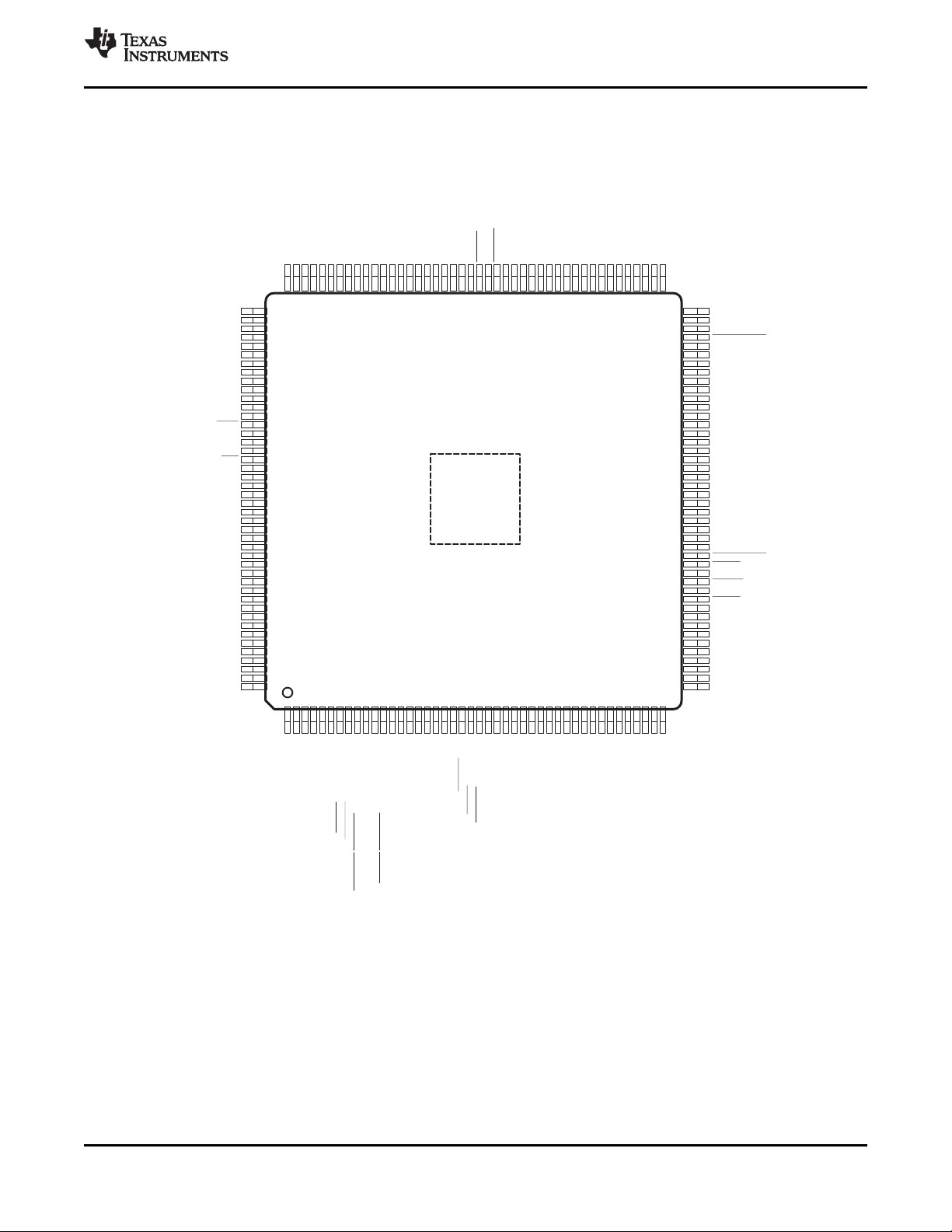
133
RSV2
134
USB0_VDDA12
135
USB0_VDDA18
136
NC
137
USB0_DP
138
USB0_DM
139
NC
140
USB0_VDDA33
141
PLL0_VDDA
142
143
OSCIN
144
145
OSCOUT
146
RESET
147
148
RSV4
149
RSV3
150
GP7[14]
152
153
154
155
156
157
158
159
160
161
162
163
164
165
166
167
168
169
170
171
172
173
174
175
176
PLL0_VSSA
OSCVSS
CV
DD
TRST
TMS
TDI
TCK
TDO
RV
DD
AFSX1/EPWMSYNCI/EPWMSYNC0/GP4[10]
DV
DD
AFSR1/GP4[13]
AXR1[8]/EPWM1A/GP4[8]
AXR1[7]/EPWM1B/GP4[7]
AXR1[6]/EPWM2A/GP4[6]
AXR1[5]/EPWM2B/GP4[5]
1
AXR1[0]/GP4[0]
2
UART0_RXD/I2C0_SDA/TM64P0_IN12/GP5[8]/BOOT[8]
3
UART0_TXD/I2C0_SCL/TM64P0_OUT12/GP5[9]/BOOT[9]
4
AXR1[10]/GP5[10]
5
DV
DD
6
AXR1[11]/GP5[11]
7
SPI1_ENA/UART2_RXD/GP5[12]
8
SPI1_SCS[0]/UART2_TXD/GP5[13]
9
SPI0_SCS[0] UART0_RTS/ /EQEP0B/GP5[4]/BOOT[4]
10
11
SPI0_CLK/EQEP1I/GP5[2]/BOOT[2]
12
13
SPI1_SOMI[0]/I2C1_SCL/GP5[5]/BOOT[5]
14
SPI1_SIMO[0]/I2C1_SDA/GP5[6]/BOOT[6]
15
16
SPI1_CLK/EQEP1S/GP5[7]/BOOT[7]
17
SPI0_SOMI[0]/EQEP0I/GP5[0]/BOOT[0]
18
19
EMA_WAIT[0]/GP2[10]
2021222324
25
EMA_BA[0]/GP1[14]
262728293031323334353637383940
41
CV
DD
SPI0_ENA UART0_CTS/ /EQEP0A/GP5[3]/BOOT[3]
DV
DD
SPI0_SIMO[0]/EQEP0S/GP5[1]/BOOT[1]
CV
DD
EMA_CS[3]/GP2[6]
EMA_OE/AXR0[13]/GP2[7]
EMA_CS[2]/GP2[5]/BOOT[15]
DV
DD
EMA_BA[1]/GP1[13]
EMA_A[10]/GP1[10]
CV
DD
EMA_A[0]/GP1[0]
EMA_A[1]/MMCSD_CLK/GP1[1]
EMA_A[2]/MMCSD_CMD/GP1[2]
EMA_A[3]/GP1[3]
DV
DD
EMA_A[4]/GP1[4]
EMA_A[5]/GP1[5]
EMA_A[6]/GP1[6]
EMA_A[7]/GP1[7]
CV
DD
EMA_A[8]/GP1[8]
EMA_A[9]/GP1[9]
EMA_A[11]/GP1[11]
EMA_A[12]/GP1[12]
DV
DD
EMA_D[0]/MMCSD_DAT[0]/GP0[0]/BOOT[12]
151
DV
DD
CV
DD
DV
DD
AHCLKX1/EPWM0B/GP3[14]
CV
DD
ACLKX1/EPWM0A/GP3[15]
ACLKR1/ECAP2/APWM2/GP4[12]
CV
DD
DV
DD
AXR1[4]/EQEP1B/GP4[4]
AXR1[3]/EQEP1A/GP4[3]
AXR1[2]/GP4[2]
AXR1[1]/GP4[1]
42
43
44
88
EMB_SDCKE
87
DV
DD
86
EMB_CLK
85
EMB_WE_DQM[1]/GP5[14]
84
EMB_D[8]/GP6[8]
83
EMB_D[9]/GP6[9]
82
EMB_D[10]/GP6[10]
81
DV
DD
80
EMB_D[11]/GP6[11]
79
EMB_D[12]/GP6[12]
78
EMB_D[13]/GP6[13]
77
CV
DD
76
EMB_D[14]/GP6[14]
75
74
EMB_D[15]/GP6[15]
73
EMB_D[0]/GP6[0]
72
EMB_D[1]/GP6[1]
71
DV
DD
70
EMB_D[2]/GP6[2]
69
CV
DD
68
EMB_D[3]/GP6[3]
67
RV
DD
66
EMB_D[4]/GP6[4]
65
DV
DD
64
EMB_D[5]/GP6[5]
63
EMB_D[6]/GP6[6]
62
EMB_D[7]/GP6[7]
61
CV
DD
60
EMB_WE_DQM[0]/GP5[15]
59
EMB_WE
58
DV
DD
57
EMB_CAS
56
CV
DD
55
EMA_WE/AXR0[12]/GP2[3]/BOOT[14]
54
EMA_D[7]/MMCSD_DAT[7]/GP0[7]/BOOT[13]
53
DV
DD
52
EMA_D[6]/MMCSD_DAT[6]/GP0[6]
51
EMA_D[5]/MMCSD_DAT[5]/GP0[5]
50
CV
DD
49
EMA_D[4]/MMCSD_DAT[4]/GP0[4]
48
EMA_D[3]/MMCSD_DAT[3]/GP0[3]
47
DV
DD
46
EMA_D[2]/MMCSD_DAT[2]/GP0[2]
45
EMA_D[1]/MMCSD_DAT[1]/GP0[1]
DV
DD
132
AMUTE1/EPWMTZ/GP4[14]
131
AFSR0/GP3[12]
130
ACLKR0/ECAP1/APWM1/GP2[15]
129
AHCLKR0/RMII_MHZ_50_CLK/GP2[14]/BOOT[11]
128
DV
DD
127
AFSX0/GP2[13]/BOOT[10]
126
ACLKX0/ECAP0/APWM0/GP2[12]
125
AHCLKX0/USB_REFCLKIN/GP2[11]
124
AXR0[11]/GP3[11]
123
UART1_TXD/AXR0[10]/GP3[10]
122
UART1_RXD/AXR0[9]/GP3[9]
121
AXR0[8]/MDIO_D/GP3[8]
120
AXR0[7]/MDIO_CLK/GP3[7]
119
118
AXR0[6]/RMII_RXER/GP3[6]
117
AXR0[5]/RMII_RXD[1]/GP3[5]
116
AXR0[4]/RMII_RXD[0]/GP3[4]
115
AXR0[3]/RMII_CRS_DV/GP3[3]
114
113
AXR0[2]/RMII_TXEN/GP3[2]
112
AXR0[1]/RMII_TXD[1]/GP3[1]
111
AXR0[0]/RMII_TXD[0]/GP3[0]
110
EMB_RAS
109
DV
DD
108
EMB_CS[0]
107
EMB_BA[0]/GP7[1]
106
EMB_BA[1]/GP7[0]
105
EMB_A[10]/GP7[12]
104
103
EMB_A[0]/GP7[2]
102
EMB_A[1]/GP7[3]
101
EMB_A[2]/GP7[4]
100
EMB_A[3]/GP7[5]
99
98
EMB_A[4]/GP7[6]
97
EMB_A[5]/GP7[7]
96
EMB_A[6]/GP7[8]
95
EMB_A[7]/GP7[9]
94
EMB_A[8]/GP7[10]
93
92
EMB_A[9]/GP7[11]91EMB_A[11]/GP7[13]
90
89
EMB_A[12]/GP3[13]
DV
DD
DV
DD
CV
DD
DV
DD
CV
DD
CV
DD
V
(177)
SS
Thermal Pad
www.ti.com
TMS320C6745, TMS320C6747
SPRS377F –SEPTEMBER 2008–REVISED JUNE 2014
Figure 3-4. Pin Map (PTP)
Submit Documentation Feedback
Product Folder Links: TMS320C6745 TMS320C6747
Device OverviewCopyright © 2008–2014, Texas Instruments Incorporated
27
Page 28
TMS320C6745, TMS320C6747
SPRS377F –SEPTEMBER 2008–REVISED JUNE 2014
3.6 Terminal Functions
to identify the external signal names, the associated pin/ball numbers along with the mechanical package
designator, the pin type (I, O, IO, OZ, or PWR), whether the pin/ball has any internal pullup/pulldown
resistors, whether the pin/ball is configurable as an IO in GPIO mode, and a functional pin description.
3.6.1 Device Reset and JTAG
Table 3-6. Reset and JTAG Terminal Functions
www.ti.com
SIGNAL NAME
RESET 146 G3 I Device reset input
AMUTE0/ RESETOUT - L4 O
TMS 152 J1 I IPU JTAG test mode select
TDI 153 J2 I IPU JTAG test data input
TDO 156 J3 O IPD JTAG test data output
TCK 155 H3 I IPU JTAG test clock
TRST 150 J4 I IPD JTAG test reset
EMU[0]/GP7[15] - J5 I/O IPU Emulation Signal
(1) I = Input, O = Output, I/O = Bidirectional, Z = High impedance, PWR = Supply voltage, GND = Ground, A = Analog signal.
Note: For multiplexed pins where functions have different types (ie., input versus output), the table reflects the pin function direction for
that particular peripheral.
(2) IPD = Internal Pulldown resistor, IPU = Internal Pullup resistor
(3) Open drain mode for RESETOUT function.
PIN NO
PTP ZKB
TYPE
(1)
(3)
(2)
PULL
RESET
IPD Reset output
JTAG
DESCRIPTION
3.6.2 High-Frequency Oscillator and PLL
Table 3-7. High-Frequency Oscillator and PLL Terminal Functions
SIGNAL NAME
EMA_CLK/OBSCLK/AHCLKR
2/GP1[15]
OSCIN 143 F2 I Oscillator input
OSCOUT 145 F1 O Oscillator output
OSCVSS 144 E2 GND Oscillator ground (for filter only)
PLL0_VDDA 141 D1 PWR PLL analog VDD(1.2-V filtered supply)
PLL0_VSSA 142 E1 GND PLL analog VSS(for filter)
(1) I = Input, O = Output, I/O = Bidirectional, Z = High impedance, PWR = Supply voltage, GND = Ground, A = Analog signal.
Note: For multiplexed pins where functions have different types (ie., input versus output), the table reflects the pin function direction for
that particular peripheral.
(2) IPD = Internal Pulldown resistor, IPU = Internal Pullup resistor
PIN NO
PTP ZKB
- R12 O IPU PLL Observation Clock
(1)
TYPE
1.2-V OSCILLATOR
1.2-V PLL
PULL
(2)
DESCRIPTION
28
Device Overview Copyright © 2008–2014, Texas Instruments Incorporated
Submit Documentation Feedback
Product Folder Links: TMS320C6745 TMS320C6747
Page 29
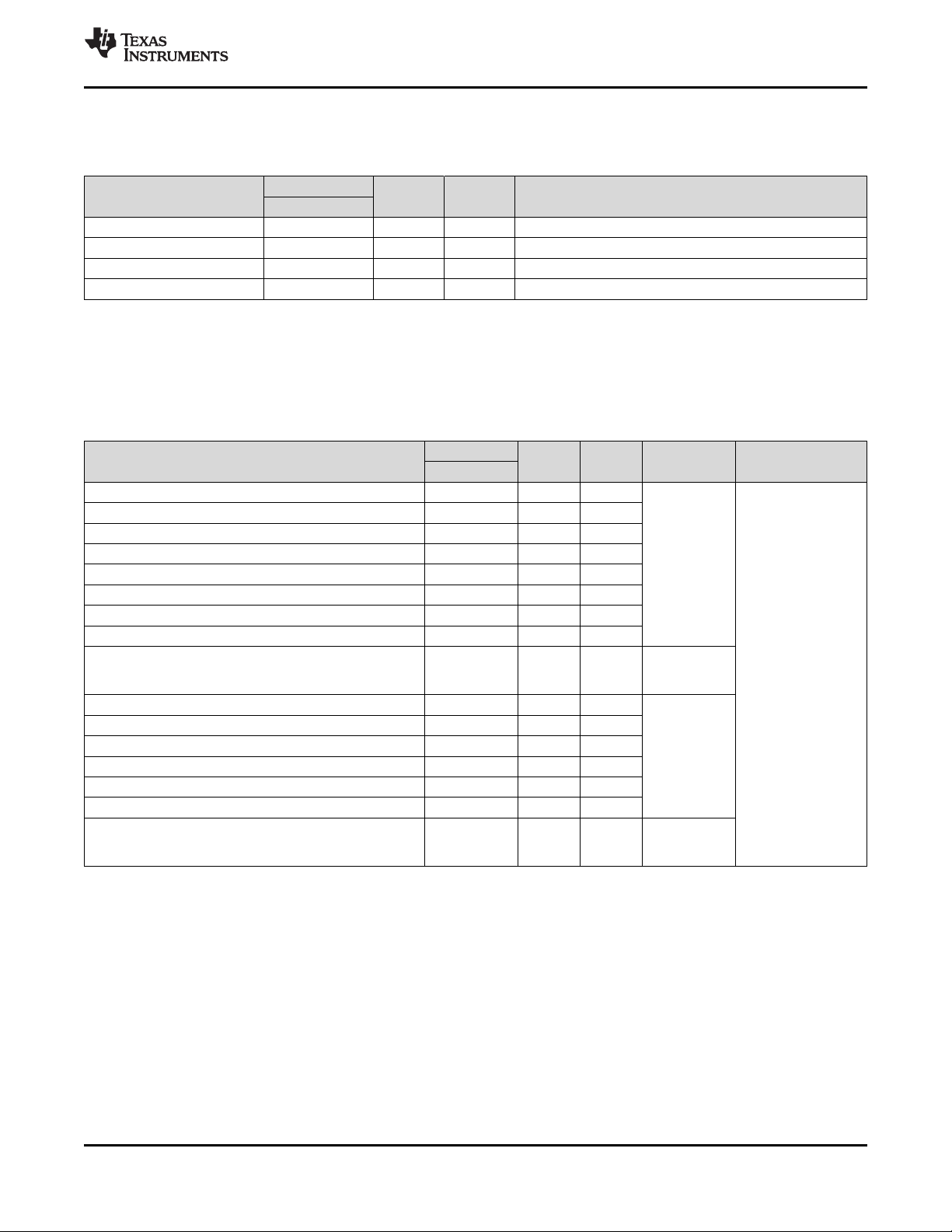
www.ti.com
3.6.3 Real-Time Clock and 32-kHz Oscillator
Table 3-8. Real-Time Clock (RTC) and 1.2-V, 32-kHz Oscillator Terminal Functions
TMS320C6745, TMS320C6747
SPRS377F –SEPTEMBER 2008–REVISED JUNE 2014
SIGNAL NAME
RTC_CVDD - G1 PWR RTC module core power (isolated from rest of chip CVDD)
RTC_XI - H1 I Low-frequency (32-kHz) oscillator receiver for real-time clock
RTC_XO - H2 O Low-frequency (32-kHz) oscillator driver for real-time clock
RTC_V
ss
(1) I = Input, O = Output, I/O = Bidirectional, Z = High impedance, PWR = Supply voltage, GND = Ground, A = Analog signal.
Note: For multiplexed pins where functions have different types (ie., input versus output), the table reflects the pin function direction for
that particular peripheral.
(2) IPD = Internal Pulldown resistor, IPU = Internal Pullup resistor
PIN NO
PTP ZKB
- G2 GND Oscillator ground (for filter)
TYPE
(1)
PULL
(2)
DESCRIPTION
3.6.4 External Memory Interface A (ASYNC, SDRAM)
Table 3-9. External Memory Interface A (EMIFA) Terminal Functions
SIGNAL NAME
EMA_D[15]/UHPI_HD[15]/LCD_D[15]/GP0[15] - M16 I/O IPD
EMA_D[14]/UHPI_HD[14]/LCD_D[14]/GP0[14] - N14 I/O IPD
EMA_D[13]/UHPI_HD[13]/LCD_D[13]/GP0[13] - N16 I/O IPD
EMA_D[12]/UHPI_HD[12]/LCD_D[12]/GP0[12] - P14 I/O IPD
EMA_D[11]/UHPI_HD[11]/LCD_D[11]/GP0[11] - P16 I/O IPD
EMA_D[10]/UHPI_HD[10]/LCD_D[10]/GP0[10] - R14 I/O IPD
EMA_D[9]/UHPI_HD[9]/LCD_D[9]/GP0[9] - T14 I/O IPD
EMA_D[8]/UHPI_HD[8]/LCD_D[8]/GP0[8] - N12 I/O IPD
EMA_D[7]/MMCSD_DAT[7]/UHPI_HD[7]/GP0[7]/BOOT[13] 54 M15 I/O IPU
EMA_D[6]/MMCSD_DAT[6]/UHPI_HD[6]/GP0[6] 52 N13 I/O IPU
EMA_D[5]/MMCSD_DAT[5]/UHPI_HD[5]/GP0[5] 51 N15 I/O IPU
EMA_D[4]/MMCSD_DAT[4]/UHPI_HD[4]/GP0[4] 49 P13 I/O IPU
EMA_D[3]/MMCSD_DAT[3]/UHPI_HD[3]/GP0[3] 48 P15 I/O IPU
EMA_D[2]/MMCSD_DAT[2]/UHPI_HD[2]/GP0[2] 46 R13 I/O IPU
EMA_D[1]/MMCSD_DAT[1]/UHPI_HD[1]/GP0[1] 45 R15 I/O IPU
EMA_D[0]/MMCSD_DAT[0]/UHPI_HD[0]/GP0[0]/BOOT[12] 44 T13 I/O IPU
PIN NO
PTP ZKB
TYPE
(1)
PULL
(2)
MUXED DESCRIPTION
UHPI, LCD,
GPIO
MMC/SD,
UHPI, GPIO,
BOOT
MMC/SD,
UHPI, GPIO
MMC/SD,
UHPI, GPIO,
BOOT
EMIFA data bus
(1) I = Input, O = Output, I/O = Bidirectional, Z = High impedance, PWR = Supply voltage, GND = Ground, A = Analog signal.
Note: The pin type shown refers to the input, output or high-impedance state of the pin function when configured as the the signal name
highlighted in bold. All multiplexed signals may enter a high-impedance state when the configured function is input-only or the configured
function supports high-Z operation. All GPIO signals can be used as input or output. For multiplexed pins where functions have different
types (ie., input versus output), the table reflects the pin function direction for that particular peripheral.
(2) IPD = Internal Pulldown resistor, IPU = Internal Pullup resistor
Device OverviewCopyright © 2008–2014, Texas Instruments Incorporated
Submit Documentation Feedback
Product Folder Links: TMS320C6745 TMS320C6747
29
Page 30
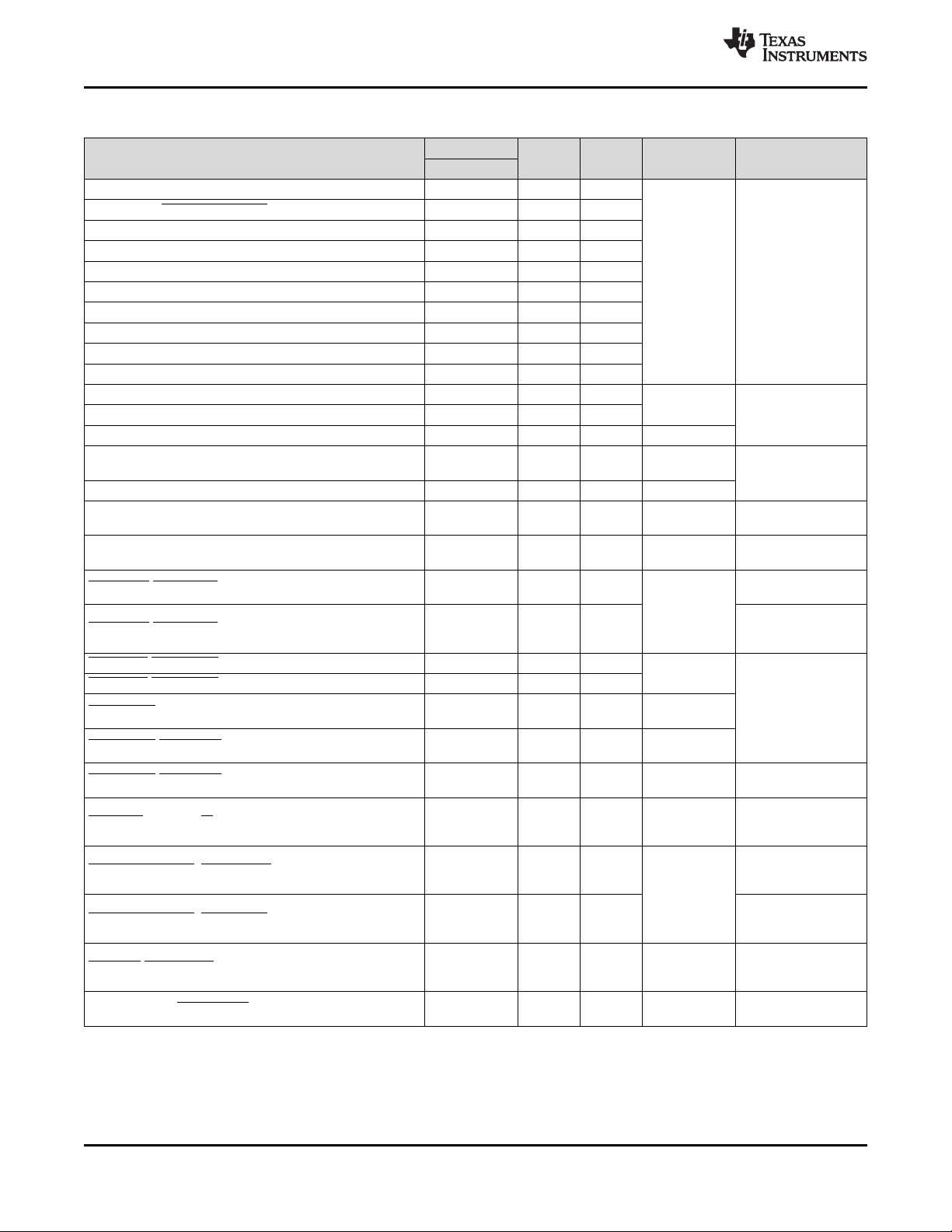
TMS320C6745, TMS320C6747
SPRS377F –SEPTEMBER 2008–REVISED JUNE 2014
Table 3-9. External Memory Interface A (EMIFA) Terminal Functions (continued)
SIGNAL NAME
PIN NO
PTP ZKB
EMA_A[12]/LCD_MCLK/GP1[12] 42 N11 O IPU
EMA_A[11] /LCD_AC_ENB_CS/GP1[11] 41 P11 O IPU
EMA_A[10]/LCD_VSYNC/GP1[10] 27 N8 O IPU
EMA_A[9]/LCD_HSYNC/GP1[9] 40 R11 O IPU
EMA_A[8]/LCD_PCLK/GP1[8] 39 T11 O IPU
EMA_A[7]/LCD_D[0]/GP1[7] 37 N10 O IPD
EMA_A[6]/LCD_D[1]/GP1[6] 36 P10 O IPD
EMA_A[5]/LCD_D[2]/GP1[5] 35 R10 O IPD
EMA_A[4]/LCD_D[3]/GP1[4] 34 T10 O IPD
EMA_A[3]/LCD_D[6]/GP1[3] 32 N9 O IPD
EMA_A[2]/MMCSD_CMD/UHPI_HCNTL1/GP1[2] 31 P9 O IPU
EMA_A[0]/LCD_D[7]/GP1[0] 29 T9 O IPD LCD, GPIO
EMA_BA[1]/LCD_D[5]/UHPI_HHWIL/GP1[13] 26 P8 O IPU
EMA_BA[0]/LCD_D[4]/GP1[14] 25 R8 O IPU LCD, GPIO
EMA_CLK/OBSCLK/AHCLKR2/GP1[15] - R12 O IPU
EMA_SDCKE/GP2[0] - T12 O IPU GPIO
EMA_RAS/EMA_CS[5]/GP2[2] - N7 O IPU
EMA_CAS/EMA_CS[4]/GP2[1] - L16 O IPU
EMA_RAS/EMA_CS[5] /GP2[2] - N7 O IPU
EMA_CAS/EMA_CS[4] /GP2[1] - L16 O IPU
EMA_CS[3]/AMUTE2/GP2[6] 21 T7 O IPU
EMA_CS[2]/UHPI_HCS/GP2[5]/BOOT[15] 23 P7 O IPU
EMA_CS[0]/UHPI_HAS/GP2[4] - T8 O IPU UHPI, GPIO
EMA_WE/UHPI_HRW/AXR0[12]/GP2[3]/BOOT[14] 55 M13 O IPU
EMA_WE_DQM[1] /UHPI_HDS2/AXR0[14]/GP2[8] - P12 O IPU
EMA_WE_DQM[0] /UHPI_HINT/AXR0[15]/GP2[9] - M14 O IPU
EMA_OE/UHPI_HDS1/AXR0[13]/GP2[7] 22 R7 O IPU
EMA_WAIT[0]/ UHPI_HRDY/GP2[10] 19 N6 I IPU UHPI, GPIO
TYPE
(1)
PULL
(2)
MUXED DESCRIPTION
LCD, GPIO EMIFA address bus
MMCSD,
UHPI, GPIO
LCD, UHPI,
GPIO
McASP2,
GPIO
EMIF A chip
select, GPIO
EMIF A
SDRAM, GPIO
McASP2,
GPIO
UHPI, GPIO,
BOOT
UHPI,
MCASP0,
GOPIO, BOOT
UHPI, McASP,
GPIO
UHPI,
McASP0,
GPIO
www.ti.com
EMIFA address busEMA_A[1]/MMCSD_CLK/UHPI_HCNTL0/GP1[1] 30 R9 O IPU
EMIFA bank address
EMIFA clock
EMIFA SDRAM clock
enable
EMIFA SDRAM row
address strobe
EMIFA SDRAM
column address
strobe
EMIFA Async Chip
Select
EMIFA SDRAM chip
select
EMIFA SDRAM write
enable
EMIFA write
enable/data mask for
EMA_D[15:8]
EMIFA write
enable/data mask for
EMA_D[7:0]
EMIFA output enable
EMIFA wait
input/interrupt
30
Device Overview Copyright © 2008–2014, Texas Instruments Incorporated
Submit Documentation Feedback
Product Folder Links: TMS320C6745 TMS320C6747
Page 31

www.ti.com
3.6.5 External Memory Interface B (only SDRAM)
Table 3-10. External Memory Interface B (EMIFB) Terminal Functions
TMS320C6745, TMS320C6747
SPRS377F –SEPTEMBER 2008–REVISED JUNE 2014
SIGNAL NAME
EMB_D[31] - G14 I/O IPD
EMB_D[30] - F15 I/O IPD
EMB_D[29] - F14 I/O IPD
EMB_D[28] - E15 I/O IPD
EMB_D[27] - E14 I/O IPD
EMB_D[26] - A14 I/O IPD
EMB_D[25] - B14 I/O IPD
EMB_D[24] - A13 I/O IPD
EMB_D[23] - L15 I/O IPD
EMB_D[22] - L14 I/O IPD
EMB_D[21] - K16 I/O IPD
EMB_D[20] - K13 I/O IPD
EMB_D[19] - J14 I/O IPD
EMB_D[18] - H15 I/O IPD
EMB_D[17] - H14 I/O IPD
EMB_D[16] - G15 I/O IPD
EMB_D[15]/GP6[15] 74 F13 I/O IPD
EMB_D[14]/GP6[14] 76 E16 I/O IPD
EMB_D[13]/GP6[13] 78 E13 I/O IPD
EMB_D[12]/GP6[12] 79 D16 I/O IPD
EMB_D[11]/GP6[11] 80 D15 I/O IPD
EMB_D[10]/GP6[10] 82 D14 I/O IPD
EMB_D[9]/GP6[9] 83 D13 I/O IPD
EMB_D[8]/GP6[8] 84 C16 I/O IPD
EMB_D[7]/GP6[7] 62 J16 I/O IPD
EMB_D[6]/GP6[6] 63 J15 I/O IPD
EMB_D[5]/GP6[5] 64 J13 I/O IPD
EMB_D[4]/GP6[4] 66 H16 I/O IPD
EMB_D[3]/GP6[3] 68 H13 I/O IPD
EMB_D[2]/GP6[2] 70 G16 I/O IPD
EMB_D[1]/GP6[1] 72 G13 I/O IPD
EMB_D[0]/GP6[0] 73 F16 I/O IPD
EMB_A[12]/GP3[13] 89 B15 O IPD
EMB_A[11]/GP7[13] 91 B12 O IPD
EMB_A[10]/GP7[12] 105 A9 O IPD
EMB_A[9]/GP7[11] 92 C12 O IPD
EMB_A[8]/GP7[10] 94 D12 O IPD
EMB_A[7]/GP7[9] 95 A11 O IPD
EMB_A[6]/GP7[8] 96 B11 O IPD
EMB_A[5]/GP7[7] 97 C11 O IPD
PIN NO
PTP ZKB
TYPE
(1)
PULL
(2)
MUXED DESCRIPTION
EMIFB SDRAM data bus
GPIO
GPIO
EMIFB SDRAM row/column
address bus
(1) I = Input, O = Output, I/O = Bidirectional, Z = High impedance, PWR = Supply voltage, GND = Ground, A = Analog signal.
Note: The pin type shown refers to the input, output or high-impedance state of the pin function when configured as the the signal name
highlighted in bold. All multiplexed signals may enter a high-impedance state when the configured function is input-only or the configured
function supports high-Z operation. All GPIO signals can be used as input or output. For multiplexed pins where functions have different
types (ie., input versus output), the table reflects the pin function direction for that particular peripheral.
(2) IPD = Internal Pulldown resistor, IPU = Internal Pullup resistor
Device OverviewCopyright © 2008–2014, Texas Instruments Incorporated
Submit Documentation Feedback
Product Folder Links: TMS320C6745 TMS320C6747
31
Page 32

TMS320C6745, TMS320C6747
SPRS377F –SEPTEMBER 2008–REVISED JUNE 2014
www.ti.com
Table 3-10. External Memory Interface B (EMIFB) Terminal Functions (continued)
SIGNAL NAME
PIN NO
PTP ZKB
EMB_A[4]/GP7[6] 98 D11 O IPD
EMB_A[3]/GP7[5] 100 A10 O IPD
EMB_A[2]/GP7[4] 101 B10 O IPD
EMB_A[1]/GP7[3] 102 C10 O IPD
EMB_A[0]/GP7[2] 103 D10 O IPD
EMB_BA[1]/GP7[0] 106 B9 O IPU
EMB_BA[0]/GP7[1] 107 C9 O IPU
EMB_CLK 86 C14 O IPU EMIF SDRAM clock
EMB_SDCKE 88 C13 O IPU EMIFB SDRAM clock enable
EMB_WE 59 K15 O IPU EMIFB write enable
EMB_RAS 110 A8 O IPU
EMB_CAS 57 L13 O IPU
EMB_CS[0] 108 D9 O IPU EMIFB SDRAM chip select 0
EMB_WE_DQM[3] - A12 O IPU
EMB_WE_DQM[2] - B13 O IPU
EMB_WE_DQM[1] /GP5[14] 85 C15 O IPU
EMB_WE_DQM[0] /GP5[15] 60 K14 O IPU
TYPE
(1)
PULL
(2)
MUXED DESCRIPTION
EMIFB SDRAM row/column
address
GPIO
EMIFB SDRAM bank address
EMIFB SDRAM row address
strobe
EMIFB column address
strobe
EMIFB write enable/data
mask for EMB_D
GPIO
32
Device Overview Copyright © 2008–2014, Texas Instruments Incorporated
Submit Documentation Feedback
Product Folder Links: TMS320C6745 TMS320C6747
Page 33

www.ti.com
3.6.6 Serial Peripheral Interface Modules (SPI0, SPI1)
Table 3-11. Serial Peripheral Interface (SPI) Terminal Functions
TMS320C6745, TMS320C6747
SPRS377F –SEPTEMBER 2008–REVISED JUNE 2014
SIGNAL NAME
SPI0_SCS[0] /UART0_RTS/EQEP0B/GP5[4]/BOOT[4] 9 N4 I/O IPU
SPI0_ENA /UART0_CTS/EQEP0A/GP5[3]/BOOT[3] 12 R5 I/O IPU
SPI0_CLK/EQEP1I/GP5[2]/BOOT[2] 11 T5 I/O IPD eQEP1, GPIO, BOOT SPI0 clock
SPI0_SIMO[0]/EQEP0S/GP5[1]/BOOT[1] 18 P6 I/O IPD
SPI0_SOMI[0]/EQEP0I/GP5[0]/BOOT[0] 17 R6 I/O IPD
SPI1_SCS[0] /UART2_TXD/GP5[13] 8 P4 I/O IPU
SPI1_ENA /UART2_RXD/GP5[12] 7 R4 I/O IPU SPI1 enable
SPI1_CLK/EQEP1S/GP5[7]/BOOT[7] 16 T6 I/O IPD eQEP1, GPIO, BOOT SPI1 clock
SPI1_SIMO[0]/I2C1_SDA/GP5[6]/BOOT[6] 14 N5 I/O IPU
SPI1_SOMI[0]/I2C1_SCL/GP5[5]/BOOT[5] 13 P5 I/O IPU
(1) I = Input, O = Output, I/O = Bidirectional, Z = High impedance, PWR = Supply voltage, GND = Ground, A = Analog signal.
Note: The pin type shown refers to the input, output or high-impedance state of the pin function when configured as the the signal name
highlighted in bold. All multiplexed signals may enter a high-impedance state when the configured function is input-only or the configured
function supports high-Z operation. All GPIO signals can be used as input or output. For multiplexed pins where functions have different
types (ie., input versus output), the table reflects the pin function direction for that particular peripheral.
(2) IPD = Internal Pulldown resistor, IPU = Internal Pullup resistor
PIN NO
PTP ZKB
SPI0
SPI1
TYPE
(1)
PULL
(2)
MUXED DESCRIPTION
UART0, EQEP0B,
GPIO, BOOT
UART0, EQEP0A,
GPIO, BOOT
eQEP0, GPIO, BOOT
UART2, GPIO
I2C1, GPIO, BOOT
SPI0 chip select
SPI0 enable
SPI0 data slave-inmaster-out
SPI0 data slaveout-master-in
SPI1 chip select
SPI1 data slave-inmaster-out
SPI1 data slaveout-master-in
Submit Documentation Feedback
Product Folder Links: TMS320C6745 TMS320C6747
Device OverviewCopyright © 2008–2014, Texas Instruments Incorporated
33
Page 34

TMS320C6745, TMS320C6747
SPRS377F –SEPTEMBER 2008–REVISED JUNE 2014
3.6.7 Enhanced Capture/Auxiliary PWM Modules (eCAP0, eCAP1, eCAP2)
The eCAP Module pins function as either input captures or auxiliary PWM 32-bit outputs, depending upon
how the eCAP module is programmed.
Table 3-12. Enhanced Capture Module (eCAP) Terminal Functions
www.ti.com
SIGNAL NAME
ACLKX0/ECAP0/APWM0/GP2[12] 126 C5 I/O IPD McASP0, GPIO
ACLKR0/ECAP1/APWM1/GP2[15] 130 B4 I/O IPD McASP0, GPIO
ACLKR1/ECAP2/APWM2/GP4[12] 165 L2 I/O IPD McASP1, GPIO
(1) I = Input, O = Output, I/O = Bidirectional, Z = High impedance, PWR = Supply voltage, GND = Ground, A = Analog signal.
Note: The pin type shown refers to the input, output or high-impedance state of the pin function when configured as the the signal name
highlighted in bold. All multiplexed signals may enter a high-impedance state when the configured function is input-only or the configured
function supports high-Z operation. All GPIO signals can be used as input or output. For multiplexed pins where functions have different
types (ie., input versus output), the table reflects the pin function direction for that particular peripheral.
(2) IPD = Internal Pulldown resistor, IPU = Internal Pullup resistor
PIN NO
PTP ZKB
eCAP0
eCAP1
eCAP2
TYPE
(1)
PULL
(2)
MUXED DESCRIPTION
enhanced capture 0
input or auxiliary
PWM 0 output
enhanced capture 1
input or auxiliary
PWM 1 output
enhanced capture 2
input or auxiliary
PWM 2 output
34
Device Overview Copyright © 2008–2014, Texas Instruments Incorporated
Submit Documentation Feedback
Product Folder Links: TMS320C6745 TMS320C6747
Page 35

TMS320C6745, TMS320C6747
www.ti.com
SPRS377F –SEPTEMBER 2008–REVISED JUNE 2014
3.6.8 Enhanced Pulse Width Modulators (eHRPWM0, eHRPWM1, eHRPWM2)
Table 3-13. Enhanced Pulse Width Modulator (eHRPWM) Terminal Functions
SIGNAL NAME
ACLKX1/EPWM0A/GP3[15] 162 K3 I/O IPD
AHCLKX1/EPWM0B/GP3[14] 160 K2 I/O IPD eHRPWM0 B output.
AMUTE1/EPWMTZ/GP4[14] 132 D4 I/O IPD
AFSX1/EPWMSYNCI/EPWMSYNCO/GP4[10] 163 K4 I/O IPD
AXR1[8]/EPWM1A/GP4[8] 168 M2 I/O IPD
AXR1[7]/EPWM1B/GP4[7] 169 M3 I/O IPD eHRPWM1 B output
AMUTE1/EPWMTZ/GP4[14] 132 D4 I/O IPD
AXR1[6]/EPWM2A/GP4[6] 170 M4 I/O IPD
AXR1[5]/EPWM2B/GP4[5] 171 N1 I/O IPD eHRPWM2 B output
AMUTE1/EPWMTZ/GP4[14] 132 D4 I/O IPD
(1) I = Input, O = Output, I/O = Bidirectional, Z = High impedance, PWR = Supply voltage, GND = Ground, A = Analog signal.
Note: The pin type shown refers to the input, output or high-impedance state of the pin function when configured as the the signal name
highlighted in bold. All multiplexed signals may enter a high-impedance state when the configured function is input-only or the configured
function supports high-Z operation. All GPIO signals can be used as input or output. For multiplexed pins where functions have different
types (ie., input versus output), the table reflects the pin function direction for that particular peripheral.
(2) IPD = Internal Pulldown resistor, IPU = Internal Pullup resistor
PIN NO
PTP ZKB
eHRPWM0
eHRPWM1
eHRPWM2
TYPE
(1)
PULL
(2)
MUXED DESCRIPTION
McASP1, GPIO
McASP1, eHRPWM1,
GPIO, eHRPWM2
McASP1, eHRPWM0,
GPIO
McASP1, GPIO
McASP1, eHRPWM0,
GPIO, eHRPWM2
McASP1, GPIO
McASP1, eHRPWM0,
GPIO, eHRPWM2
eHRPWM0 A output
(with high-resolution)
eHRPWM0 trip zone
input
Sync input to
eHRPWM0 module or
sync output to
external PWM
eHRPWM1 A (with
high-resolution)
eHRPWM1 trip zone
input
eHRPWM2 A (with
high-resolution)
eHRPWM2 trip zone
input
Submit Documentation Feedback
Product Folder Links: TMS320C6745 TMS320C6747
Device OverviewCopyright © 2008–2014, Texas Instruments Incorporated
35
Page 36

TMS320C6745, TMS320C6747
SPRS377F –SEPTEMBER 2008–REVISED JUNE 2014
3.6.9 Enhanced Quadrature Encoder Pulse Module (eQEP)
Table 3-14. Enhanced Quadrature Encoder Pulse Module (eQEP) Terminal Functions
www.ti.com
SIGNAL NAME
SPI0_ENA/UART0_CTS/EQEP0A/GP5[3]/BOOT[3] 12 R5 I IPU
SPI0_SCS[0]/UART0_RTS/EQEP0B/GP5[4]/BOOT[4] 9 N4 I IPU
SPI0_SOMI[0]/EQEP0I/GP5[0]/BOOT[0] 17 R6 I IPD
SPI0_SIMO[0]/EQEP0S/GP5[1]/BOOT[1] 18 P6 I IPD eQEP0 strobe
AXR1[3]/EQEP1A/GP4[3] 174 P1 I IPD
AXR1[4]/EQEP1B/GP4[4] 173 N2 I IPD
SPI0_CLK/EQEP1I/GP5[2]/BOOT[2] 11 T5 I IPD SPI0, GPIO, BOOT eQEP1 index
SPI1_CLK/EQEP1S/GP5[7]/BOOT[7] 16 T6 I IPD SPI1, GPIO, BOOT eQEP1 strobe
(1) I = Input, O = Output, I/O = Bidirectional, Z = High impedance, PWR = Supply voltage, GND = Ground, A = Analog signal.
Note: The pin type shown refers to the input, output or high-impedance state of the pin function when configured as the the signal name
highlighted in bold. All multiplexed signals may enter a high-impedance state when the configured function is input-only or the configured
function supports high-Z operation. All GPIO signals can be used as input or output. For multiplexed pins where functions have different
types (ie., input versus output), the table reflects the pin function direction for that particular peripheral.
(2) IPD = Internal Pulldown resistor, IPU = Internal Pullup resistor
PIN NO
PTP ZKB
eQEP0
eQEP1
TYPE
(1)
PULL
(2)
MUXED DESCRIPTION
SPI0, UART0,
GPIO, BOOT
SPI0, GPIO, BOOT
McASP1, GPIO
eQEP0A quadrature
input
eQEP0B quadrature
input
eQEP0 index
eQEP1A quadrature
input
eQEP1B quadrature
input
36
Device Overview Copyright © 2008–2014, Texas Instruments Incorporated
Submit Documentation Feedback
Product Folder Links: TMS320C6745 TMS320C6747
Page 37

www.ti.com
3.6.10 Boot
TMS320C6745, TMS320C6747
SPRS377F –SEPTEMBER 2008–REVISED JUNE 2014
PULL
(1)
(3)
EMIFA, UHPI,
McASP0, GPIO
EMIFA, MMC/SD,
UHPI, GPIO
McASP0, EMAC,
GPIO
UART0, I2C0,
Timer0, GPIO
UART0, I2C0,
Timer0, GPIO
SPI1, I2C1, GPIO
SPI0, UART0,
eQEP0, GPIO
SPI0, UART0,
eQEP0, GPIO
SPI0, eQEP0, GPIO
MUXED DESCRIPTION
BOOT[14]
BOOT[13]
BOOT[11]
BOOT[9]
BOOT[8]
BOOT[6]
BOOT[4]
BOOT[3]
BOOT[1]
Table 3-15. Boot Terminal Functions
SIGNAL NAME
EMA_CS[2]/UHPI_HCS/GP2[5]/BOOT[15] 23 P7 I IPU EMIFA, UHPI, GPIO BOOT[15]
EMA_WE/UHPI_HRW/AXR0[12]/GP2[3]/BOOT[14] 55 M13 I IPU
EMA_D[7]/MMCSD_DAT[7]/UHPI_HD[7]/GP0[7]/BOOT[13] 54 M15 I IPU
EMA_D[0]/MMCSD_DAT[0]/UHPI_HD[0]/GP0[0]/BOOT[12] 44 T13 I IPU BOOT[12]
AHCLKR0/RMII_MHZ_50_CLK/GP2[14]/BOOT[11] 129 A4 I IPD
AFSX0/GP2[13]/BOOT[10] 127 D5 I IPD McASP0, GPIO BOOT[10]
UART0_TXD/I2C0_SCL/TM64P0_OUT12/GP5[9]/BOOT[9] 3 P3 I IPU
UART0_RXD/I2C0_SDA/TM64P0_IN12/GP5[8]/BOOT[8] 2 R3 I IPU
SPI1_CLK/EQEP1S/GP5[7]/BOOT[7] 16 T6 I IPD SPI1, eQEP1, GPIO BOOT[7]
SPI1_SIMO[0]/I2C1_SDA/GP5[6]/BOOT[6] 14 N5 I IPU
SPI1_SOMI[0]/I2C1_SCL/GP5[5]/BOOT[5] 13 P5 I IPU BOOT[5]
SPI0_SCS[0]/UART0_RTS/EQEP0B/GP5[4]/BOOT[4] 9 N4 I IPU
SPI0_ENA/UART0_CTS/EQEP0A/GP5[3]/BOOT[3] 12 R5 I IPU
SPI0_CLK/EQEP1I/GP5[2]/BOOT[2] 11 T5 I IPD SPI0, eQEP1, GPIO BOOT[2]
SPI0_SIMO[0]/EQEP0S/GP5[1]/BOOT[1] 18 P6 I IPD
SPI0_SOMI[0]/EQEP0I/GP5[0]/BOOT[0] 17 R6 I IPD BOOT[0]
(1) Boot decoding will be defined in the ROM datasheet.
(2) I = Input, O = Output, I/O = Bidirectional, Z = High impedance, PWR = Supply voltage, GND = Ground, A = Analog signal.
Note: The pin type shown refers to the input, output or high-impedance state of the pin function when configured as the the signal name
highlighted in bold. All multiplexed signals may enter a high-impedance state when the configured function is input-only or the configured
function supports high-Z operation. All GPIO signals can be used as input or output. For multiplexed pins where functions have different
types (ie., input versus output), the table reflects the pin function direction for that particular peripheral.
(3) IPD = Internal Pulldown resistor, IPU = Internal Pullup resistor
PIN NO
PTP ZKB
TYPE
(2)
Submit Documentation Feedback
Product Folder Links: TMS320C6745 TMS320C6747
Device OverviewCopyright © 2008–2014, Texas Instruments Incorporated
37
Page 38

TMS320C6745, TMS320C6747
SPRS377F –SEPTEMBER 2008–REVISED JUNE 2014
3.6.11 Universal Asynchronous Receiver/Transmitters (UART0, UART1, UART2)
Table 3-16. Universal Asynchronous Receiver/Transmitter (UART) Terminal Functions
www.ti.com
SIGNAL NAME
PIN NO
PTP ZKB
TYPE
(1)
PULL
(2)
MUXED DESCRIPTION
UART0
UART0_RXD/I2C0_SDA/TM64P0_IN12/GP5[8]/BOOT[8] 2 R3 I IPU
UART0_TXD/I2C0_SCL/TM64P0_OUT12/GP5[9]/BOOT[9] 3 P3 O IPU
SPI0_SCS[0]/ UART0_RTS /EQEP0B/GP5[4]/BOOT[4] 9 N4 O IPU
SPI0_ENA/ UART0_CTS /EQEP0A/GP5[3]/BOOT[3] 12 R5 I IPU
I2C0, BOOT,
Timer0, GPIO,
I2C0, Timer0,
GPIO, BOOT
SPI0, eQEP0,
GPIO, BOOT
UART0 receive
data
UART0 transmit
data
UART0 ready-tosend output
UART0 clear-tosend input
UART1
UART1_RXD/AXR0[9]/GP3[9]
UART1_TXD/AXR0[10]/GP3[10]
(3)
(3)
122 C6 I IPD
McASP0, GPIO
123 D6 O IPD
UART1 receive
data
UART1 transmit
data
UART2
SPI1_ENA/UART2_RXD/GP5[12] 7 R4 I IPU
SPI1, GPIO
SPI1_SCS[0]/UART2_TXD/GP5[13] 8 P4 O IPU
UART2 receive
data
UART2 transmit
data
(1) I = Input, O = Output, I/O = Bidirectional, Z = High impedance, PWR = Supply voltage, GND = Ground, A = Analog signal.
Note: The pin type shown refers to the input, output or high-impedance state of the pin function when configured as the the signal name
highlighted in bold. All multiplexed signals may enter a high-impedance state when the configured function is input-only or the configured
function supports high-Z operation. All GPIO signals can be used as input or output. For multiplexed pins where functions have different
types (ie., input versus output), the table reflects the pin function direction for that particular peripheral.
(2) IPD = Internal Pulldown resistor, IPU = Internal Pullup resistor
(3) As these signals are internally pulled down while the device is in reset, it is necessary to externally pull them high with resistors if
UART1 boot mode is used. Please see the TMS320C6745/C6747 DSP Technical Reference Manual (SPRUH91) for more for details on
entering UART1 boot mode.
38
Device Overview Copyright © 2008–2014, Texas Instruments Incorporated
Submit Documentation Feedback
Product Folder Links: TMS320C6745 TMS320C6747
Page 39
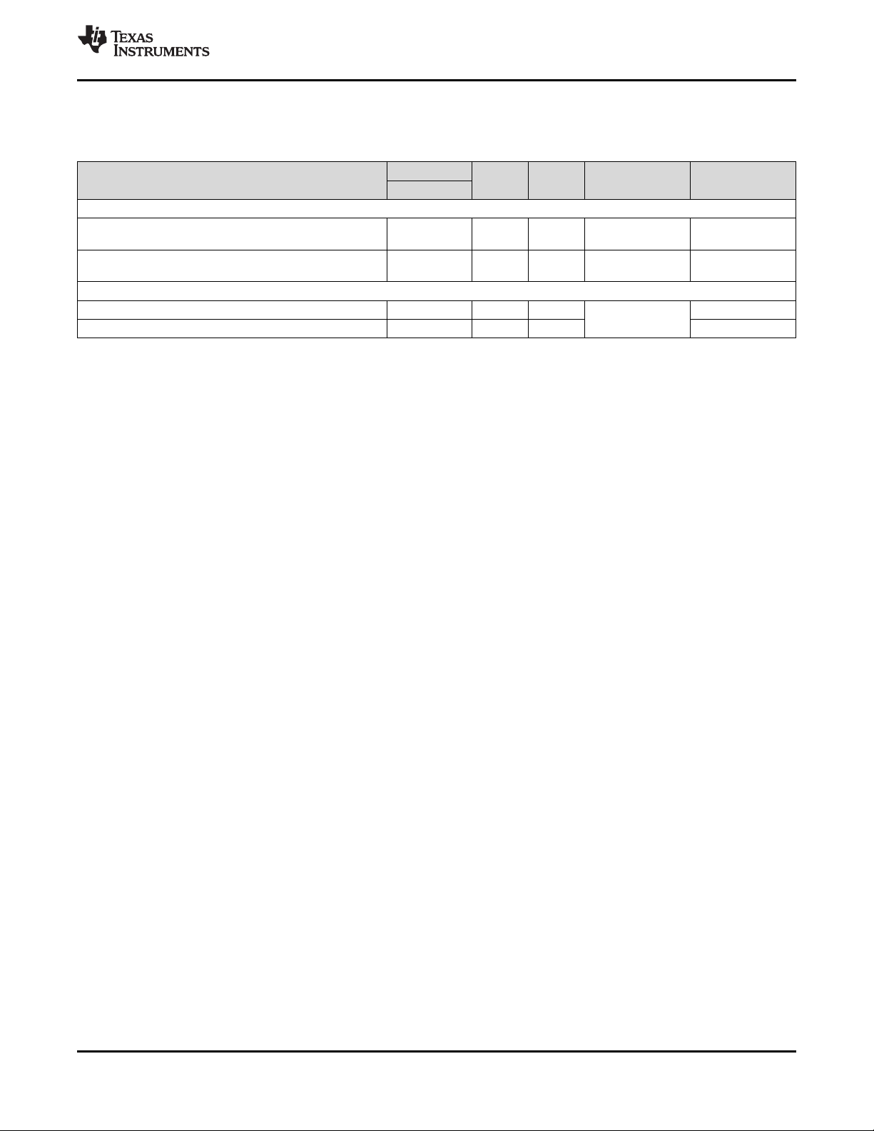
www.ti.com
3.6.12 Inter-Integrated Circuit Modules (I2C0, I2C1)
Table 3-17. Inter-Integrated Circuit (I2C) Terminal Functions
TMS320C6745, TMS320C6747
SPRS377F –SEPTEMBER 2008–REVISED JUNE 2014
SIGNAL NAME
UART0_RXD/I2C0_SDA/TM64P0_IN12/GP5[8]/BOOT[8] 2 R3 I/O IPU
UART0_TXD/I2C0_SCL/TM64P0_OUT12/GP5[9]/BOOT[9] 3 P3 I/O IPU
SPI1_SIMO[0]/I2C1_SDA/GP5[6]/BOOT[6] 14 N5 I/O IPU
SPI1_SOMI[0]/I2C1_SCL/GP5[5]/BOOT[5] 13 P5 I/O IPU I2C1 serial clock
(1) I = Input, O = Output, I/O = Bidirectional, Z = High impedance, PWR = Supply voltage, GND = Ground, A = Analog signal.
Note: The pin type shown refers to the input, output or high-impedance state of the pin function when configured as the the signal name
highlighted in bold. All multiplexed signals may enter a high-impedance state when the configured function is input-only or the configured
function supports high-Z operation. All GPIO signals can be used as input or output. For multiplexed pins where functions have different
types (ie., input versus output), the table reflects the pin function direction for that particular peripheral.
(2) IPD = Internal Pulldown resistor, IPU = Internal Pullup resistor
PIN NO
PTP ZKB
I2C0
I2C1
TYPE
(1)
PULL
(2)
UART0, Timer0,
GPIO, BOOT
UART0, Timer0,
GPIO, BOOT
SPI1, GPIO,
BOOT
MUXED DESCRIPTION
I2C0 serial data
I2C0 serial clock
I2C1 serial data
Submit Documentation Feedback
Product Folder Links: TMS320C6745 TMS320C6747
Device OverviewCopyright © 2008–2014, Texas Instruments Incorporated
39
Page 40

TMS320C6745, TMS320C6747
SPRS377F –SEPTEMBER 2008–REVISED JUNE 2014
3.6.13 Timers
Table 3-18. Timers Terminal Functions
www.ti.com
SIGNAL NAME
UART0_RXD/I2C0_SDA/TM64P0_IN12/GP5[8]/BOOT[8] 2 R3 I IPU
UART0_TXD/I2C0_SCL/TM64P0_OUT12/GP5[9]/BOOT[9] 3 P3 O IPU
No external pins. The Timer1 peripheral pins are not pinned out as external pins.
(1) I = Input, O = Output, I/O = Bidirectional, Z = High impedance, PWR = Supply voltage, GND = Ground, A = Analog signal.
Note: The pin type shown refers to the input, output or high-impedance state of the pin function when configured as the the signal name
highlighted in bold. All multiplexed signals may enter a high-impedance state when the configured function is input-only or the configured
function supports high-Z operation. All GPIO signals can be used as input or output. For multiplexed pins where functions have different
types (ie., input versus output), the table reflects the pin function direction for that particular peripheral.
(2) IPD = Internal Pulldown resistor, IPU = Internal Pullup resistor
PIN NO
PTP ZKB
TIMER0
TIMER1 (Watchdog )
TYPE
(1)
PULL
(2)
UART0, I2C0,
GPIO, BOOT
MUXED DESCRIPTION
Timer0 lower input
Timer0 lower
output
40
Device Overview Copyright © 2008–2014, Texas Instruments Incorporated
Submit Documentation Feedback
Product Folder Links: TMS320C6745 TMS320C6747
Page 41

TMS320C6745, TMS320C6747
www.ti.com
SPRS377F –SEPTEMBER 2008–REVISED JUNE 2014
3.6.14 Universal Host-Port Interface (UHPI)
Note:
The UHPI module requires 16 data pins for the host port interface to function. Therefore on the PTP, the
UHPI is not available.
Table 3-19. Universal Host-Port Interface (UHPI) Terminal Functions
SIGNAL NAME
EMA_D[15]/UHPI_HD[15]/LCD_D[15]/GP0[15] - M16 I/O IPD
EMA_D[14]/UHPI_HD[14]/LCD_D[14]/GP0[14] - N14 I/O IPD
EMA_D[13]/UHPI_HD[13]/LCD_D[13]/GP0[13] - N16 I/O IPD
EMA_D[12]/UHPI_HD[12]/LCD_D[12]/GP0[12] - P14 I/O IPD
EMA_D[11]/UHPI_HD[11]/LCD_D[11]/GP0[11] - P16 I/O IPD
EMA_D[10]/UHPI_HD[10]/LCD_D[10]/GP0[10] - R14 I/O IPD
EMA_D[9]/UHPI_HD[9]/LCD_D[9]/GP0[9] - T14 I/O IPD
EMA_D[8]/UHPI_HD[8]/LCD_D[8]/GP0[8] - N12 I/O IPD
EMA_D[7]/MMCSD_DAT[7]/UHPI_HD[7]/GP0[7]/
BOOT[13]
EMA_D[6]/MMCSD_DAT[6]/UHPI_HD[6]/GP0[6] - N13 I/O IPU
EMA_D[5]/MMCSD_DAT[5]/UHPI_HD[5]/GP0[5] - N15 I/O IPU
EMA_D[4]/MMCSD_DAT[4]/UHPI_HD[4]/GP0[4] - P13 I/O IPU
EMA_D[3]/MMCSD_DAT[3]/UHPI_HD[3]/GP0[3] - P15 I/O IPU
EMA_D[2]/MMCSD_DAT[2]/UHPI_HD[2]/GP0[2] - R13 I/O IPU
EMA_D[1]/MMCSD_DAT[1]/UHPI_HD[1]/GP0[1] - R15 I/O IPU
EMA_D[0]/MMCSD_DAT[0]/UHPI_HD[0]/GP0[0]/
BOOT[12]
EMA_A[2]/MMCSD_CMD/UHPI_HCNTL1/GP1[2] - P9 I/O IPU EMIFA,
EMA_A[1]/MMCSD_CLK/UHPI_HCNTL0/GP1[1] - R9 I/O IPU
EMA_BA[1]/LCD_D[5]/UHPI_HHWIL/GP1[13] - P8 I/O IPU EMIFA, LCD, GPIO
EMA_WE/UHPI_HRW /AXR0[12]/GP2[3]/BOOT[14] - M13 I/O IPU
EMA_CS[2]/ UHPI_HCS /GP2[5]/BOOT[15] - P7 I/O IPU
EMA_WE_DQM[1]/ UHPI_HDS2 /AXR0[14]/GP2[8] - P12 I/O IPU
EMA_OE/ UHPI_HDS1 /AXR0[13]/GP2[7] - R7 I/O IPU
EMA_WE_DQM[0]/ UHPI_HINT /AXR0[15]/GP2[9] - M14 I/O IPU UHPI host interrupt
EMA_WAIT[0]/ UHPI_HRDY /GP2[10] - N6 I/O IPU
EMA_CS[0]/ UHPI_HAS /GP2[4] - T8 I/O IPU
(1) I = Input, O = Output, I/O = Bidirectional, Z = High impedance, PWR = Supply voltage, GND = Ground, A = Analog signal.
Note: The pin type shown refers to the input, output or high-impedance state of the pin function when configured as the the signal name
highlighted in bold. All multiplexed signals may enter a high-impedance state when the configured function is input-only or the configured
function supports high-Z operation. All GPIO signals can be used as input or output. For multiplexed pins where functions have different
types (ie., input versus output), the table reflects the pin function direction for that particular peripheral.
(2) IPD = Internal Pulldown resistor, IPU = Internal Pullup resistor
PIN NO
PTP ZKB
- M15 I/O IPU
- T13 I/O IPU
TYPE
1)
(
PULL
(2)
MUXED DESCRIPTION
EMIFA, LCD, GPIO
EMIFA, MMC/SD,
GPIO, BOOT
EMIFA, MMC/SD,
GPIO
EMIFA, MMC/SD,
GPIO, BOOT
MMCSD_CMD,
GPIO
EMIFA, McASP,
GPIO, BOOT
EMIFA, GPIO,
BOOT
EMIFA, McASP0,
GPIO
EMIFA, GPIO
UHPI data bus
UHPI access control
UHPI half-word
identification control
UHPI read/write
UHPI chip select
UHPI data strobe
UHPI ready
UHPI address
strobe
Submit Documentation Feedback
Product Folder Links: TMS320C6745 TMS320C6747
Device OverviewCopyright © 2008–2014, Texas Instruments Incorporated
41
Page 42

TMS320C6745, TMS320C6747
SPRS377F –SEPTEMBER 2008–REVISED JUNE 2014
3.6.15 Multichannel Audio Serial Ports (McASP0, McASP1, McASP2)
Table 3-20. Multichannel Audio Serial Ports (McASPs) Terminal Functions
www.ti.com
SIGNAL NAME
McASP0
EMA_WE_DQM[0]/UHPI_HINT/AXR0[15]/GP2[9] - M14 I/O IPU
EMA_WE_DQM[1]/UHPI_HDS2/AXR0[14]/GP2[8] - P12 I/O IPU
EMA_OE/UHPI_HDS1/AXR0[13]/GP2[7] 22 R7 I/O IPU
EMA_WE/UHPI_HRW/AXR0[12]/GP2[3]/BOOT[14] 55 M13 I/O IPU
AXR0[11]/AXR2[0]/GP3[11] 124 A5 I/O IPD
UART1_TXD/AXR0[10]/GP3[10] 123 D6 I/O IPD UART1, GPIO
UART1_RXD/AXR0[9]/GP3[9] 122 C6 I/O IPD UART1, GPIO
AXR0[8]/MDIO_D/GP3[8] 121 B6 I/O IPU
AXR0[7]/MDIO_CLK/GP3[7] 120 A6 I/O IPD
AXR0[6]/RMII_RXER/ACLKR2/GP3[6] 118 D7 I/O IPD
AXR0[5]/RMII_RXD[1]/AFSX2/GP3[5] 117 C7 I/O IPD
AXR0[4]/RMII_RXD[0]/AXR2[1]/GP3[4] 116 B7 I/O IPD
AXR0[3]/RMII_CRS_DV/AXR2[2]/GP3[3] 115 A7 I/O IPD
AXR0[2]/RMII_TXEN/AXR2[3]/GP3[2] 113 D8 I/O IPD
AXR0[1]/RMII_TXD[1]/ACLKX2/GP3[1] 112 C8 I/O IPD
AXR0[0]/RMII_TXD[0]/AFSR2/GP3[0] 111 B8 I/O IPD
AHCLKX0/AHCLKX2/USB_REFCLKIN/GP2[11] 125 B5 I/O IPD
ACLKX0/ECAP0/APWM0/GP2[12] 126 C5 I/O IPD eCAP0, GPIO
AFSX0/GP2[13]/BOOT[10] 127 D5 I/O IPD GPIO, BOOT
AHCLKR0/RMII_MHZ_50_CLK/GP2[14]/BOOT[11] 129 A4 I/O IPD
ACLKR0/ECAP1/APWM1/GP2[15] 130 B4 I/O IPD eCAP1, GPIO
AFSR0/GP3[12] 131 C4 I/O IPD GPIO
AMUTE0/RESETOUT - L4 O IPD RESETOUT
(1) I = Input, O = Output, I/O = Bidirectional, Z = High impedance, PWR = Supply voltage, GND = Ground, A = Analog signal.
Note: The pin type shown refers to the input, output or high-impedance state of the pin function when configured as the the signal name
highlighted in bold. All multiplexed signals may enter a high-impedance state when the configured function is input-only or the configured
function supports high-Z operation. All GPIO signals can be used as input or output. For multiplexed pins where functions have different
types (ie., input versus output), the table reflects the pin function direction for that particular peripheral.
(2) IPD = Internal Pulldown resistor, IPU = Internal Pullup resistor
PIN NO
PTP ZKB
TYPE
(1)
PULL
(2)
MUXED DESCRIPTION
EMIFA, UHPI,
GPIO
EMIFA, UHPI,
GPIO, BOOT
McASP2,
GPIO
MDIO, GPIO
EMAC,
McASP2,
GPIO
McASP2, USB,
GPIO
EMAC, GPIO,
BOOT
McASP0 serial
data
McASP0
transmit master
clock
McASP0
transmit bit
clock
McASP0
transmit frame
sync
McASP0 receive
master clock
McASP0 receive
bit clock
McASP0 receive
frame sync
McASP0 mute
output
42
Device Overview Copyright © 2008–2014, Texas Instruments Incorporated
Submit Documentation Feedback
Product Folder Links: TMS320C6745 TMS320C6747
Page 43

TMS320C6745, TMS320C6747
www.ti.com
SPRS377F –SEPTEMBER 2008–REVISED JUNE 2014
Table 3-20. Multichannel Audio Serial Ports (McASPs) Terminal Functions (continued)
SIGNAL NAME
PIN NO
PTP ZKB
McASP1
AXR1[11]/GP5[11] 6 T4 I/O IPU
AXR1[10]/GP5[10] 4 N3 I/O IPU
AXR1[9]/GP4[9] - M1 I/O IPD
AXR1[8]/EPWM1A/GP4[8] 168 M2 I/O IPD
AXR1[7]/EPWM1B/GP4[7] 169 M3 I/O IPD
AXR1[6]/EPWM2A/GP4[6] 170 M4 I/O IPD
AXR1[5]/EPWM2B/GP4[5] 171 N1 I/O IPD
AXR1[4]/EQEP1B/GP4[4] 173 N2 I/O IPD
AXR1[3]/EQEP1A/GP4[3] 174 P1 I/O IPD
AXR1[2]/GP4[2] 175 P2 I/O IPD
AXR1[0]/GP4[0] 1 T3 I/O IPD
AHCLKX1/EPWM0B/GP3[14] 160 K2 I/O IPD
ACLKX1/EPWM0A/GP3[15] 162 K3 I/O IPD
AFSX1/EPWMSYNCI/EPWMSYNCO/GP4[10] 163 K4 I/O IPD
AHCLKR1/GP4[11] - L1 I/O IPD GPIO
ACLKR1/ECAP2/APWM2/GP4[12] 165 L2 I/O IPD eCAP2, GPIO
AFSR1/GP4[13] 166 L3 I/O IPD GPIO
AMUTE1/EPWMTZ/GP4[14] 132 D4 O IPD
McASP2
AXR0[0]/RMII_TXD[0]/AFSR2/GP3[0] - B8 I/O IPD
AXR0[2]/RMII_TXEN/AXR2[3]/GP3[2] - D8 I/O IPD
AXR0[3]/RMII_CRS_DV/AXR2[2]/GP3[3] - A7 I/O IPD
AXR0[4]/RMII_RXD[0]/AXR2[1]/GP3[4] - B7 I/O IPD
AXR0[11]/AXR2[0]/GP3[11] - A5 I/O IPD
AHCLKX0/AHCLKX2/USB_REFCLKIN/GP2[11] - B5 I/O IPD
AXR0[1]/RMII_TXD[1]/ACLKX2/GP3[1] - C8 I/O IPD
AXR0[5]/RMII_RXD[1]/AFSX2/GP3[5] - C7 I/O IPD
EMA_CLK/OBSCLK/AHCLKR2/GP1[15] - R12 I/O IPU EMIFA, GPIO
TYPE
(1)
PULL
(2)
MUXED DESCRIPTION
GPIO
eHRPWM1 A,
GPIO
eHRPWM1 B,
GPIO
eHRPWM2 A,
GPIO
eHRPWM2 B,
GPIO
eQEP, GPIO
GPIOAXR1[1]/GP4[1] 176 R2 I/O IPD
eHRPWM0,
GPIO
eHRPWM0,
GPIO
eHRPWM0,
GPIO
eHRPWM0,
eHRPWM1,
eHRPWM2,
GPIO
McASP0,
EMAC, GPIO
McASP0,
GPIO
McASP0, USB,
GPIO
McASP0,
EMAC, GPIO
McASP1 serial
data
McASP1
transmit master
clock
McASP1
transmit bit
clock
McASP1
transmit frame
sync
McASP1 receive
master clock
McASP1 receive
bit clock
McASP1 receive
frame sync
McASP1 mute
output
McASP2 serial
data
McASP2
transmit master
clock
McASP2
transmit bit
clock
McASP2
transmit frame
sync
McASP2 receive
master clock
Submit Documentation Feedback
Product Folder Links: TMS320C6745 TMS320C6747
Device OverviewCopyright © 2008–2014, Texas Instruments Incorporated
43
Page 44

TMS320C6745, TMS320C6747
SPRS377F –SEPTEMBER 2008–REVISED JUNE 2014
Table 3-20. Multichannel Audio Serial Ports (McASPs) Terminal Functions (continued)
SIGNAL NAME
PIN NO
PTP ZKB
AXR0[6]/RMII_RXER/ACLKR2/GP3[6] - D7 I/O IPD
EMA_CS[3]/AMUTE2/GP2[6] - T7 O IPU EMIFA, GPIO
TYPE
(1)
PULL
(2)
MUXED DESCRIPTION
McASP0,
EMAC, GPIO
www.ti.com
McASP2 receive
bit clock
McASP2 mute
output
44
Device Overview Copyright © 2008–2014, Texas Instruments Incorporated
Submit Documentation Feedback
Product Folder Links: TMS320C6745 TMS320C6747
Page 45
www.ti.com
3.6.16 Universal Serial Bus Modules (USB0, USB1)
Table 3-21. Universal Serial Bus (USB) Terminal Functions
TMS320C6745, TMS320C6747
SPRS377F –SEPTEMBER 2008–REVISED JUNE 2014
SIGNAL NAME
PIN NO
PTP ZKB
TYPE
(1)
PULL
(2)
DESCRIPTION
USB0 2.0 OTG (USB0)
USB0_DM 138 G4 A USB0 PHY data minus
USB0_DP 137 F4 A USB0 PHY data plus
USB0_VDDA33 140 H5 PWR USB0 PHY 3.3-V supply
USB0_VDDA18 135 E3 PWR USB0 PHY 1.8-V supply input
USB0 PHY 1.2-V LDO output for bypass cap
USB0_VDDA12
(3)
134 C3 PWR
For proper device operation, this pin is
recommended to be connected via a 0.22-μF
capacitor to VSS (GND), even if USB0 is not
being used.
USB0_ID - D2 A USB0 PHY identification (mini-A or mini-B plug)
USB0_VBUS - D3 A USB0 bus voltage
USB0_DRVVBUS/GP4[15] - E4 O IPD USB0 controller VBUS control output
AHCLKX0/AHCLKX2/USB_REFCLKIN/GP2[11] 125 B5 I IPD USB_REFCLKIN. Optional clock input
USB1 1.1 OHCI (USB1)
USB1_DM - B3 A USB1 PHY data minus
USB1_DP - A3 A USB1 PHY data plus
USB1_VDDA33 - C1 PWR USB1 PHY 3.3-V supply
USB1_VDDA18 - C2 PWR USB1 PHY 1.8-V supply
AHCLKX0/AHCLKX2/USB_REFCLKIN/GP2[11] 125 B5 I IPD USB_REFCLKIN. Optional clock input.
(1) I = Input, O = Output, I/O = Bidirectional, Z = High impedance, PWR = Supply voltage, GND = Ground, A = Analog signal.
Note: The pin type shown refers to the input, output or high-impedance state of the pin function when configured as the the signal name
highlighted in bold. All multiplexed signals may enter a high-impedance state when the configured function is input-only or the configured
function supports high-Z operation. All GPIO signals can be used as input or output. For multiplexed pins where functions have different
types (ie., input versus output), the table reflects the pin function direction for that particular peripheral.
(2) IPD = Internal Pulldown resistor, IPU = Internal Pullup resistor
(3) Core power supply LDO output for USB PHY.
Submit Documentation Feedback
Product Folder Links: TMS320C6745 TMS320C6747
Device OverviewCopyright © 2008–2014, Texas Instruments Incorporated
45
Page 46

TMS320C6745, TMS320C6747
SPRS377F –SEPTEMBER 2008–REVISED JUNE 2014
3.6.17 Ethernet Media Access Controller (EMAC)
Table 3-22. Ethernet Media Access Controller (EMAC) Terminal Functions
www.ti.com
SIGNAL NAME
AHCLKR0/RMII_MHZ_50_CLK/GP2[14]/BOOT[11] 129 A4 I/O IPD McASP0, GPIO, BOOT
AXR0[6]/RMII_RXER/ACLKR2/GP3[6] 118 D7 I IPD
AXR0[5]/RMII_RXD[1]/AFSX2/GP3[5] 117 C7 I IPD
AXR0[4]/RMII_RXD[0]/AXR2[1]/GP3[4] 116 B7 I IPD
AXR0[3]/RMII_CRS_DV/AXR2[2]/GP3[3] 115 A7 I IPD
AXR0[2]/RMII_TXEN/AXR2[3]/GP3[2] 113 D8 O IPD
AXR0[1]/RMII_TXD[1]/ACLKX2/GP3[1] 112 C8 O IPD
AXR0[0]/RMII_TXD[0]/AFSR2/GP3[0] 111 B8 O IPD
AXR0[8]/MDIO_D/GP3[8] 121 B6 I/O IPU
AXR0[7]/MDIO_CLK/GP3[7] 120 A6 O IPD
(1) I = Input, O = Output, I/O = Bidirectional, Z = High impedance, PWR = Supply voltage, GND = Ground, A = Analog signal.
Note: The pin type shown refers to the input, output or high-impedance state of the pin function when configured as the the signal name
highlighted in bold. All multiplexed signals may enter a high-impedance state when the configured function is input-only or the configured
function supports high-Z operation. All GPIO signals can be used as input or output. For multiplexed pins where functions have different
types (ie., input versus output), the table reflects the pin function direction for that particular peripheral.
(2) IPD = Internal Pulldown resistor, IPU = Internal Pullup resistor
PIN NO
PTP ZKB
RMII
MDIO
TYPE
(1)
PULL
(2)
McASP0, McASP2, GPIO
McASP0, GPIO MDIO data clock
MUXED DESCRIPTION
EMAC 50-MHz
clock input or
output
EMAC RMII
receiver error
EMAC RMII
receive data
EMAC RMII carrier
sense data valid
EMAC RMII
transmit enable
EMAC RMII trasmit
data
46
Device Overview Copyright © 2008–2014, Texas Instruments Incorporated
Submit Documentation Feedback
Product Folder Links: TMS320C6745 TMS320C6747
Page 47

www.ti.com
3.6.18 Multimedia Card/Secure Digital (MMC/SD)
Table 3-23. Multimedia Card/Secure Digital (MMC/SD) Terminal Functions
TMS320C6745, TMS320C6747
SPRS377F –SEPTEMBER 2008–REVISED JUNE 2014
SIGNAL NAME
EMA_A[1]/MMCSD_CLK/UHPI_HCNTL0/GP1[1] 30 R9 O IPU
EMA_A[2]/MMCSD_CMD/UHPI_HCNTL1/GP1[2] 31 P9 I/O IPU
EMA_D[7]/MMCSD_DAT[7]/UHPI_HD[7]/GP0[7]/BOOT[13] 54 M15 I/O IPU
EMA_D[6]/MMCSD_DAT[6]/UHPI_HD[6]/GP0[6] 52 N13 I/O IPU
EMA_D[5]/MMCSD_DAT[5]/UHPI_HD[5]/GP0[5] 51 N15 I/O IPU
EMA_D[4]/MMCSD_DAT[4]/UHPI_HD[4]/GP0[4] 49 P13 I/O IPU
EMA_D[3]/MMCSD_DAT[3]/UHPI_HD[3]/GP0[3] 48 P15 I/O IPU
EMA_D[2]/MMCSD_DAT[2]/UHPI_HD[2]/GP0[2] 46 R13 I/O IPU
EMA_D[1]/MMCSD_DAT[1]/UHPI_HD[1]/GP0[1] 45 R15 I/O IPU
EMA_D[0]/MMCSD_DAT[0]/UHPI_HD[0]/GP0[0]/BOOT[12] 44 T13 I/O IPU
(1) I = Input, O = Output, I/O = Bidirectional, Z = High impedance, PWR = Supply voltage, GND = Ground, A = Analog signal.
Note: The pin type shown refers to the input, output or high-impedance state of the pin function when configured as the the signal name
highlighted in bold. All multiplexed signals may enter a high-impedance state when the configured function is input-only or the configured
function supports high-Z operation. All GPIO signals can be used as input or output. For multiplexed pins where functions have different
types (ie., input versus output), the table reflects the pin function direction for that particular peripheral.
(2) IPD = Internal Pulldown resistor, IPU = Internal Pullup resistor
PIN NO
PTP ZKB
TYPE
(1)
PULL
(2)
MUXED DESCRIPTION
EMIFA, UHPI, GPIO
EMIFA, UHPI, GPIO,
BOOT
EMIFA, UHPI, GPIO
EMIFA, UHPI, GPIO,
BOOT
MMCSD Clock
MMCSD
Command
MMC/SD data
Submit Documentation Feedback
Product Folder Links: TMS320C6745 TMS320C6747
Device OverviewCopyright © 2008–2014, Texas Instruments Incorporated
47
Page 48

TMS320C6745, TMS320C6747
SPRS377F –SEPTEMBER 2008–REVISED JUNE 2014
3.6.19 Liquid Crystal Display Controller (LCD)
Table 3-24. Liquid Crystal Display Controller (LCD) Terminal Functions
www.ti.com
SIGNAL NAME
EMA_D[15]/UHPI_HD[15]/LCD_D [15]/GP0[15] - M16 I/O IPD
EMA_D[14]/UHPI_HD[14]/LCD_D[14]/GP0[14] - N14 I/O IPD
EMA_D[13]/UHPI_HD[13]/LCD_D[13]/GP0[13] - N16 I/O IPD
EMA_D[12]/UHPI_HD[12]/LCD_D[12]/GP0[12] - P14 I/O IPD
EMA_D[11]/UHPI_HD[11]/LCD_D[11 ]/GP0[11] - P16 I/O IPD
EMA_D[10]/UHPI_HD[10]/LCD_D[10]/GP0[10] - R14 I/O IPD
EMA_D[9]/UHPI_HD[9]/LCD_D[9]/GP0[9] - T14 I/O IPD
EMA_D[8]/UHPI_HD[8]/LCD_D[8]/GP0[8] - N12 I/O IPD
EMA_A[0]/LCD_D[7]/GP1[0] - T9 I/O IPD
EMA_A[3]/LCD_D[6]/GP1[3] - N9 I/O IPD
EMA_BA[1]/LCD_D[5]/UHPI_HHWIL/GP1[13] - P8 I/O IPU
EMA_BA[0]/LCD_D[4]/GP1[14] - R8 I/O IPU
EMA_A[4]/LCD_D[3]/GP1[4] - T10 I/O IPD
EMA_A[5]/LCD_D[2]/GP1[5] - R10 I/O IPD
EMA_A[6]/LCD_D[1]/GP1[6] - P10 I/O IPD
EMA_A[7]/LCD_D[0]/GP1[7] - N10 I/O IPD
EMA_A[8]/LCD_PCLK/GP1[8] - T11 O IPU LCD pixel clock
EMA_A[9]/LCD_HSYNC/GP1[9] - R11 O IPU LCD horizontal sync
EMA_A[10]/LCD_VSYNC/GP1[10] - N8 O IPU LCD vertical sync
EMA_A[11]/ LCD_AC_ENB_CS /GP1[11] - P11 O IPU
EMA_A[12]/LCD_MCLK/GP1[12] - N11 O IPU LCD memory clock
(1) I = Input, O = Output, I/O = Bidirectional, Z = High impedance, PWR = Supply voltage, GND = Ground, A = Analog signal.
Note: The pin type shown refers to the input, output or high-impedance state of the pin function when configured as the the signal name
highlighted in bold. All multiplexed signals may enter a high-impedance state when the configured function is input-only or the configured
function supports high-Z operation. All GPIO signals can be used as input or output. For multiplexed pins where functions have different
types (ie., input versus output), the table reflects the pin function direction for that particular peripheral.
(2) IPD = Internal Pulldown resistor, IPU = Internal Pullup resistor
PIN NO
PTP ZKB
TYPE
(1)
PULL
(2)
EMIFA, UHPI,
GPIO
EMIFA, GPIO
EMIFA, UHPI,
GPIO
EMIFA, GPIO
MUXED DESCRIPTION
LCD data bus
LCD AC bias enable
chip select
48
Device Overview Copyright © 2008–2014, Texas Instruments Incorporated
Submit Documentation Feedback
Product Folder Links: TMS320C6745 TMS320C6747
Page 49

www.ti.com
3.6.20 General Purpose Input Output (GPIO)
Table 3-25. General Purpose Input Output Terminal Functions
TMS320C6745, TMS320C6747
SPRS377F –SEPTEMBER 2008–REVISED JUNE 2014
SIGNAL NAME
EMA_D[15]/UHPI_HD[15]/LCD_D[15]/GP0[15] - M16 I/O IPD
EMA_D[14]/UHPI_HD[14]/LCD_D[14]/GP0[14] - N14 I/O IPD
EMA_D[13]/UHPI_HD[13]/LCD_D[13]/GP0[13] - N16 I/O IPD
EMA_D[12]/UHPI_HD[12]/LCD_D[12]/GP0[12] - P14 I/O IPD
EMA_D[11]/UHPI_HD[11]/LCD_D[11]/GP0[11] - P16 I/O IPD
EMA_D[10]/UHPI_HD[10]/LCD_D[10]/GP0[10] - R14 I/O IPD
EMA_D[9]/UHPI_HD[9]/LCD_D[9]/GP0[9] - T14 I/O IPD
EMA_D[8]/UHPI_HD[8]/LCD_D[8]/GP0[8] - N12 I/O IPD
EMA_D[7]/MMCSD_DAT[7]/UHPI_HD[7]/GP0[7]/BOOT[13] 54 M15 I/O IPU
EMA_D[6]/MMCSD_DAT[6]/UHPI_HD[6]/GP0[6] 52 N13 I/O IPU
EMA_D[5]/MMCSD_DAT[5]/UHPI_HD[5]/GP0[5] 51 N15 I/O IPU
EMA_D[4]/MMCSD_DAT[4]/UHPI_HD[4]/GP0[4] 49 P13 I/O IPU
EMA_D[3]/MMCSD_DAT[3]/UHPI_HD[3]/GP0[3] 48 P15 I/O IPU
EMA_D[2]/MMCSD_DAT[2]/UHPI_HD[2]/GP0[2] 46 R13 I/O IPU
EMA_D[1]/MMCSD_DAT[1]/UHPI_HD[1]/GP0[1] 45 R15 I/O IPU
EMA_D[0]/MMCSD_DAT[0]/UHPI_HD[0]/GP0[0]/BOOT[12] 44 T13 I/O IPU
EMA_CLK/OBSCLK/AHCLKR2/GP1[15] - R12 O IPU EMIFA, McASP2
EMA_BA[0]/LCD_D[4]/GP1[14] 25 R8 O IPU EMIFA, LCD
EMA_BA[1]/LCD_D[5]/UHPI_HHWIL/GP1[13] 26 P8 O IPU
EMA_A[12]/LCD_MCLK/GP1[12] 42 N11 O IPU
EMA_A[11]/ LCD_AC_ENB_CS/GP1[11] 41 P11 O IPU
EMA_A[10]/LCD_VSYNC/GP1[10] 27 N8 O IPU
EMA_A[9]/LCD_HSYNC/GP1[9] 40 R11 O IPU
EMA_A[8]/LCD_PCLK/GP1[8] 39 T11 O IPU
EMA_A[7]/LCD_D[0]/GP1[7] 37 N10 O IPD
EMA_A[6]/LCD_D[1]/GP1[6] 36 P10 O IPD
EMA_A[5]/LCD_D[2]/GP1[5] 35 R10 O IPD
EMA_A[4]/LCD_D[3]/GP1[4] 34 T10 O IPD
EMA_A[3]/LCD_D[6]/GP1[3] 32 N9 O IPD
EMA_A[2]/MMCSD_CMD/UHPI_HCNTL1/GP1[2] 31 P9 O IPU
EMA_A[1]/MMCSD_CLK/UHPI_HCNTL0/GP1[1] 30 R9 O IPU
EMA_A[0]/LCD_D[7]/GP1[0] 29 T9 O IPD EMIFA, LCD
(1) I = Input, O = Output, I/O = Bidirectional, Z = High impedance, PWR = Supply voltage, GND = Ground, A = Analog signal.
Note: The pin type shown refers to the input, output or high-impedance state of the pin function when configured as the the signal name
highlighted in bold. All multiplexed signals may enter a high-impedance state when the configured function is input-only or the configured
function supports high-Z operation. All GPIO signals can be used as input or output. For multiplexed pins where functions have different
types (ie., input versus output), the table reflects the pin function direction for that particular peripheral.
(2) IPD = Internal Pulldown resistor, IPU = Internal Pullup resistor
PIN NO
PTP ZKB
GP0
GP1
TYPE
(1)
PULL
(2)
MUXED DESCRIPTION
EMIFA, UHPI,
LCD
EMIFA, MMC/SD,
UHPI, BOOT
EMIFA, MMC/SD,
UHPI
EMIFA, MMC/SD,
UHPI, BOOT
EMIFA, LCD,
UHPI
EMIFA, LCD
EMIFA, MMCSD,
UHPI
GPIO Bank 0
GPIO Bank 1
Submit Documentation Feedback
Product Folder Links: TMS320C6745 TMS320C6747
Device OverviewCopyright © 2008–2014, Texas Instruments Incorporated
49
Page 50

TMS320C6745, TMS320C6747
SPRS377F –SEPTEMBER 2008–REVISED JUNE 2014
Table 3-25. General Purpose Input Output Terminal Functions (continued)
SIGNAL NAME
PIN NO
PTP ZKB
GP2
ACLKR0/ECAP1/APWM1/GP2[15] 130 b4 I/O IPD McASP0, eCAP1
AHCLKR0/RMII_MHZ_50_CLK/GP2[14]/BOOT[11] 129 A4 I/O IPD
AFSX0/GP2[13]/BOOT[10] 127 D5 I/O IPD McASP0, BOOT
ACLKX0/ECAP0/APWM0/GP2[12] 126 CD I/O IPD McASP0, eCAP0
AHCLKX0/AHCLKX2/USB_REFCLKIN/GP2[11] 125 B5 I IPD
EMA_WAIT[0]/ UHPI_HRDY/GP2[10] 19 N6 I IPU EMIFA, UHPI
EMA_WE_DQM[0] /UHPI_HINT/AXR0[15]/GP2[9] - M14 O IPU
EMA_WE_DQM[1] /UHPI_HDS2/AXR0[14]/GP2[8] - P12 O IPU
EMA_OE /UHPI_HDS1/AXR0[13]/GP2[7] 22 R7 O IPU
EMA_CS[3] /AMUTE2/GP2[6] 21 T7 O IPU EMIFA, McASP2
EMA_CS[2] /UHPI_HCS/GP2[5]/BOOT[15] 23 P7 O IPU
EMA_CS[0] /UHPI_HAS/GP2[4] - T8 O IPU EMIFA, UHPI
EMA_WE /UHPI_HRW/AXR0[12]/GP2[3]/BOOT[14] 55 M13 O IPU
EMA_RAS /EMA_CS[5]/GP2[2] - N7 O IPU
EMA_CAS /EMA_CS[4]/GP2[1] - L16 O IPU
EMA_SDCKE/GP2[0] - T12 O IPU EMIFA
GP3
ACLKX1/EPWM0A/GP3[15] 162 K3 I/O IPD
AHCLKX1/EPWM0B/GP3[14] 160 K2 I/O IPD
EMB_A[12]/GP3[13] 89 B15 O IPD EMIFB
AFSR0/GP3[12] 131 C4 I/O IPD McASP0
AXR0[11]/AXR2[0]/GP3[11] - A5 I/O IPD EMAC,
UART1_TXD/AXR0[10]/GP3[10] 123 D6 I/O IPD
UART1_RXD/AXR0[9]/GP3[9] 122 C6 I/O IPD
AXR0[8]/MDIO_D/GP3[8] 121 B6 I/0 IPU
AXR0[7]/MDIO_CLK/GP3[7] 120 A6 O IPD
AXR0[6]/RMII_RXER/ACLKR2/GP3[6] 118 D7 I IPD
AXR0[5]/RMII_RXD[1]/AFSX2/GP3[5] 117 C7 I IPD
AXR0[4]/RMII_RXD[0]/AXR2[1]/GP3[4] 116 B7 I IPD
AXR0[3]/RMII_CRS_DV/AXR2[2]/GP3[3] 115 A7 I IPD
AXR0[2]/RMII_TXEN/AXR2[3]/GP3[2] 113 D8 O IPD
AXR0[1]/RMII_TXD[1]/ACLKX2/GP3[1] 112 C8 O IPD
AXR0[0]/RMII_TXD[0]/AFSR2/GP3[0] 111 B8 O IPD
TYPE
(1)
PULL
(2)
MUXED DESCRIPTION
McASP0, EMAC,
BOOT
McASP0,
McASP2, USB
EMIFA, UHPI,
McASP0
EMIFA, UHPI,
BOOT
EMIFA, UHPI,
MCASP0, BOOT
EMIFA, EMIFA
McASP1,
eHRPWM0
UART1, McASP0
McASP0, MDIO
McASP0, EMAC,
McASP2
www.ti.com
GPIO Bank 2
GPIO Bank 3
50
Device Overview Copyright © 2008–2014, Texas Instruments Incorporated
Submit Documentation Feedback
Product Folder Links: TMS320C6745 TMS320C6747
Page 51

TMS320C6745, TMS320C6747
www.ti.com
SPRS377F –SEPTEMBER 2008–REVISED JUNE 2014
Table 3-25. General Purpose Input Output Terminal Functions (continued)
SIGNAL NAME
PIN NO
PTP ZKB
GP4
USB0_DRVVBUS/GP4[15] - E4 O IPD USB0
AMUTE1/EPWMTZ/GP4[14] 132 D4 O IPD
AFSR1/GP4[13] 166 L3 I/O IPD McASP1
ACLKR1/ECAP2/APWM2/GP4[12] 165 L2 I/O IPD McASP1, eCAP2
AHCLKR1/GP4[11] - L1 I/O IPD McASP1
AFSX1/EPWMSYNCI/EPWMSYNCO/GP4[10] 163 K4 I/O IPD
AXR1[9]/GP4[9] - M1 I/O IPD McASP1
AXR1[8]/EPWM1A/GP4[8] 168 M2 I/O IPD
AXR1[7]/EPWM1B/GP4[7] 169 M3 I/O IPD
AXR1[6]/EPWM2A/GP4[6] 170 M4 I/O IPD
AXR1[5]/EPWM2B/GP4[5] 171 N1 I/O IPD
AXR1[4]/EQEP1B/GP4[4] 173 N2 I/O IPD
AXR1[3]/EQEP1A/GP4[3] 174 P1 I/O IPD
AXR1[2]/GP4[2] 175 P2 I/O IPD
AXR1[0]/GP4[0] 1 T3 I/O IPD
GP5
EMB_WE_DQM[0]/GP5[15] 60 K14 O IPU
EMB_WE_DQM[1]/GP5[14] 85 C15 O IPU
SPI1_SCS[0]/UART2_TXD/GP5[13] 8 P4 O IPU
SPI1_ENA/UART2_RXD/GP5[12] 7 R4 I IPU
AXR1[11]/GP5[11] 6 T4 I/O IPU
AXR1[10]/GP5[10] 4 N3 I/O IPU
UART0_TXD/I2C0_SCL/TM64P0_OUT12/GP5[9]/BOOT[9] 2 R3 I IPU
UART0_RXD/I2C0_SDA/TM64P0_IN12/GP5[8]/BOOT[8] 3 P3 O IPU
SPI1_CLK/EQEP1S/GP5[7]/BOOT[7] 16 T6 I IPD
SPI1_SIMO[0]/I2C1_SDA/GP5[6]/BOOT[6] 14 N5 I/O IPU
SPI1_SOMI[0]/I2C1_SCL/GP5[5]/BOOT[5] 13 P5 I/O IPU
SPI0_SCS[0]/UART0_RTS/EQEP0B/GP5[4]/BOOT[4] 9 N4 I IPU
SPI0_ENA/UART0_CTS/EQEP0A/GP5[3]/BOOT[3] 12 R5 I IPU
SPI0_CLK/EQEP1I/GP5[2]/BOOT[2] 11 T5 I IPD
SPI0_SIMO[0]/EQEP0S/GP5[1]/BOOT[1] 18 P6 I IPD
SPI0_SOMI[0]/EQEP0I/GP5[0]/BOOT[0] 17 R6 I IPD
TYPE
(1)
PULL
(2)
MUXED DESCRIPTION
McASP1,
eHRPWM0,
eHRPWM1,
eHRPWM2
McASP1,
eHRPWM0
McASP1,
eHRPWM1 A
McASP1,
eHRPWM1 B
McASP1,
eHRPWM2 A
McASP1,
eHRPWM2 B
McASP1, eQEP
McASP1AXR1[1]/GP4[1] 176 R2 I/O IPD
EMIFB
SPI1, UART2
McASP1
UART0, I2C0,
BOOT
SPI1, eQEP1,
BOOT
SPI1, I2C1,
BOOT
SPI0, UART0,
eQEP0, BOOT
SPI0, eQEP1,
BOOT
SPI0, eQEP0,
BOOT
GPIO Bank 4
GPIOBank 5
Submit Documentation Feedback
Product Folder Links: TMS320C6745 TMS320C6747
Device OverviewCopyright © 2008–2014, Texas Instruments Incorporated
51
Page 52

TMS320C6745, TMS320C6747
SPRS377F –SEPTEMBER 2008–REVISED JUNE 2014
www.ti.com
Table 3-25. General Purpose Input Output Terminal Functions (continued)
SIGNAL NAME
PIN NO
PTP ZKB
GP6
EMB_D[15]/GP6[15] 74 F13 I/O IPD
EMB_D[14]/GP6[14] 76 E`6 I/O IPD
EMB_D[13]/GP6[13] 78 E13 I/O IPD
EMB_D[12]/GP6[12] 79 D16 I/O IPD
EMB_D[11]/GP6[11] 80 D15 I/O IPD
EMB_D[10]/GP6[10] 82 D14 I/O IPD
EMB_D[9]/GP6[9] 83 D13 I/O IPD
EMB_D[8]/GP6[8] 84 C16 I/O IPD
EMB_D[7]/GP6[7] 62 J16 I/O IPD
EMB_D[6]/GP6[6] 63 J15 I/O IPD
EMB_D[5]/GP6[5] 64 J13 I/O IPD
EMB_D[4]/GP6[4] 66 H16 I/O IPD
EMB_D[3]/GP6[3] 68 H13 I/O IPD
EMB_D[2]/GP6[2] 70 G16 I/O IPD
EMB_D[1]/GP6[1] 72 G13 I/O IPD
EMB_D[0]/GP6[0] 73 F16 I/O IPD
GP7
EMU[0]/GP7[15] - J5 I/O IPU JTAG
RTCK/ GP7[14]
(3)
157 K1 I/O IPD
EMB_A[11]/GP7[13] 91 B12 O IPD
EMB_A[10]/GP7[12] 105 A9 O IPD
EMB_A[9]/GP7[11] 92 C12 O IPD
EMB_A[8]/GP7[10] 94 D12 O IPD
EMB_A[7]/GP7[9] 95 A11 O IPD
EMB_A[6]/GP7[8] 96 B11 O IPD
EMB_A[5]/GP7[7] 97 C11 O IPD
EMB_A[4]/GP7[6] 98 D11 O IPD
EMB_A[3]/GP7[5] 100 A10 O IPD
EMB_A[2]/GP7[4] 101 B10 O IPD
EMB_A[1]/GP7[3] 102 C10 O IPD
EMB_A[0]/GP7[2] 103 D10 O IPD
EMB_BA[0]/GP7[1] 107 C9 O IPU
EMB_BA[1]/GP7[0] 106 B9 O IPU
(3) GP7[14] is initially configured as a reserved function after reset and will not be in a predictable state. This signal will only be stable after
the GPIO configuration for this pin has been completed. Users should carefully consider the system implications of this pin being in an
unknown state after reset.
TYPE
(1)
PULL
(2)
MUXED DESCRIPTION
EMIFB GPIO Bank 6
General-Purpose
IO signal
EMIFB GPIO Bank 7
3.6.21 Reserved and No Connect
Table 3-26. Reserved and No Connect Terminal Functions
SIGNAL NAME
RSV1 - F7 -
(1) PWR = Supply voltage.
52
Device Overview Copyright © 2008–2014, Texas Instruments Incorporated
PIN NO
PTP ZKB
TYPE
Submit Documentation Feedback
Product Folder Links: TMS320C6745 TMS320C6747
(1)
DESCRIPTION
Reserved. (Leave unconnected, do not connect to power or
ground.)
Page 53

www.ti.com
SPRS377F –SEPTEMBER 2008–REVISED JUNE 2014
Table 3-26. Reserved and No Connect Terminal Functions (continued)
SIGNAL NAME
RSV2 133 B1 PWR
RSV3 149 - PWR
RSV4 148 - I
NC 136 F3 - No Connect (leave unconnected)
NC 139 H4 - No Connect (leave unconnected)
PIN NO
PTP ZKB
TYPE
(1)
Reserved. For proper device operation, this pin must be tied either
directly to CVDD or left unconnected [do not connect to ground
(VSS)].
Reserved. For proper device operation, this pin must be tied
directly to CVDD.
Reserved. For proper device operation, this pin must be tied low or
to CVDD.
DESCRIPTION
TMS320C6745, TMS320C6747
Submit Documentation Feedback
Product Folder Links: TMS320C6745 TMS320C6747
Device OverviewCopyright © 2008–2014, Texas Instruments Incorporated
53
Page 54

TMS320C6745, TMS320C6747
SPRS377F –SEPTEMBER 2008–REVISED JUNE 2014
3.6.22 Supply and Ground
Table 3-27. Supply and Ground Terminal Functions
www.ti.com
SIGNAL NAME
10, 20, 28,
38, 50, 56,
CVDD (Core supply)
RVDD (Internal RAM supply) 67, 159 H6, H12 PWR Internal ram supply voltage pins
DVDD (I/O supply)
VSS (Ground) 177
(1) PWR = Supply voltage, GND - Ground.
61, 69, 77,
93, 104, 114,
147, 154,
161, 167
5, 15, 24, 33,
43, 47, 53,
58, 65, 71,
75, 81, 87,
90, 99, 109,
119, 128,
151, 158,
164, 172
PIN NO
PTP ZKB
F6,G6, G7,
G10, G11,
H7, H10,
H11, J6, J7,
J10, J11,
J12, K6, K7,
K10, K11,L6
B16, E5, E8,
E9, E12, F5,
F11, F12,
G5, G12, K5,
K12, L5, L11,
L12, M5, M8,
M9, M12, R1,
R16
A1, A2, A15,
A16,
B2,
E6, E7, E10,
E11,
F8, F9, F10,
G8, G9,
H8, H9,
J8, J9,
K8, K9,
L7, L8, L9,
L10,
M6, M7, M10,
M11,
T1, T2, T15,
T16
(1)
TYPE
PWR Core supply voltage pins
PWR I/O supply voltage pins
GND Ground pins
DESCRIPTION
54
Device Overview Copyright © 2008–2014, Texas Instruments Incorporated
Submit Documentation Feedback
Product Folder Links: TMS320C6745 TMS320C6747
Page 55
www.ti.com
SPRS377F –SEPTEMBER 2008–REVISED JUNE 2014
3.6.23 Unused USB0 (USB2.0) and USB1 (USB1.1) Pin Configurations
If one or both USB modules on the device are not used, then some of the power supplies to those
modules may not be required. This can eliminate the requirement for a 1.8V power supply to the USB
modules. The required pin configurations for unused USB modules are shown below.
Table 3-28. Unused USB0 and USB1 Pin Configurations
TMS320C6745, TMS320C6747
SIGNAL NAME Configuration
USB0_DM No connect Use as USB0 function
USB0_DP No connect Use as USB0 function
USB0_VDDA33 No connect 3.3V
USB0_VDDA18 No connect 1.8V
USB0_ID No connect Use as USB0 function
USB0_VBUS No connect Use as USB0 function
USB0_DRVVBUS/GP4[15] No connect or use as alternate function Use as USB0 or alternate function
USB0_VDDA12 Internal USB0 PHY output connected to an external 0.22μF filter capacitor
USB1_DM No connect VSS
USB1_DP No connect VSS
USB1_VDDA33 No connect No connect
USB1_VDDA18 No connect No connect
AHCLKX0/AHCLKX2/USB_REFCLKIN/
GP2[11]
(When USB0 and USB1 are not used)
No connect or use as alternate function Use as USB0 or alternate function
Configuration
(When USB0 is used
and USB1 is not used)
Submit Documentation Feedback
Product Folder Links: TMS320C6745 TMS320C6747
Device OverviewCopyright © 2008–2014, Texas Instruments Incorporated
55
Page 56

TMS320C6745, TMS320C6747
SPRS377F –SEPTEMBER 2008–REVISED JUNE 2014
4 Device Configuration
4.1 Boot Modes
This device supports a variety of boot modes through an internal ROM bootloader. This device does not
support dedicated hardware boot modes; therefore, all boot modes utilize the internal ROM. The input
states of the BOOT pins are sampled and latched into the BOOTCFG register, which is part of the system
configuration (SYSCFG) module, when device reset is deasserted. Boot mode selection is determined by
the values of the BOOT pins.
The following boot modes are supported:
• NAND Flash boot
– 8-bit NAND
– 16-bit NAND
• NOR Flash boot
– NOR Direct boot (8-bit or 16-bit)
– NOR Legacy boot (8-bit or 16-bit)
– NOR AIS boot (8-bit or 16-bit)
• HPI Boot [C6747 only]
• I2C0 / I2C1 Boot
– EEPROM (Master Mode)
– External Host (Slave Mode)
• SPI0 / SPI1 Boot
– Serial Flash (Master Mode)
– SERIAL EEPROM (Master Mode)
– External Host (Slave Mode)
• UART0 / UART1 / UART2 Boot
– External Host
www.ti.com
56
Device Configuration Copyright © 2008–2014, Texas Instruments Incorporated
Submit Documentation Feedback
Product Folder Links: TMS320C6745 TMS320C6747
Page 57

www.ti.com
4.2 SYSCFG Module
The following system level features of the chip are controlled by the SYSCFG peripheral:
• Readable Device, Die, and Chip Revision ID
• Control of Pin Multiplexing
• Priority of bus accesses different bus masters in the system
• Capture at power on reset the chip BOOT[15:0] pin values and make them available to software
• Special case settings for peripherals:
– Locking of PLL controller settings
– Default burst sizes for EDMA3 TC0 and TC1
– Selection of the source for the eCAP module input capture (including on chip sources)
– McASP AMUTEIN selection and clearing of AMUTE status for the three McASP peripherals
– Control of the reference clock source and other side-band signals for both of the integrated USB
PHYs
– Clock source selection for EMIFA and EMIFB
• Selects the source of emulation suspend signal (from DSP) of peripherals supporting this function.
Many registers are accessible only by a host (DSP) when it is operating in its privileged mode. (ex. from
the kernel, but not from user space code).
TMS320C6745, TMS320C6747
SPRS377F –SEPTEMBER 2008–REVISED JUNE 2014
Table 4-1. System Configuration (SYSCFG) Module Register Access
BYTE ADDRESS ACRONYM REGISTER DESCRIPTION ACCESS
0x01C1 4000 REVID Revision Identification Register —
0x01C14008 DIEIDR0 Device Identification Register 0 —
0x01C1 400C DIEIDR1 Device Identification Register 1 —
0x01C1 4010 DIEIDR2 Device Identification Register 2 —
0x01C1 4014 DIEIDR3 Device Identification Register 3 —
0x01C1 4018 DEVIDR0 JTAG Identification Register —
0x01C1 4020 BOOTCFG Boot Configuration Register Privileged mode
0x01C1 4024 CHIPREVID Silicon Revision Identification Register Privileged mode
0x01C1 4038 KICK0R Kick 0 Register Privileged mode
0x01C1 403C KICK1R Kick 1 Register Privileged mode
0x01C1 4040 HOST0CFG Host 0 Configuration Register —
0x01C1 4044 HOST1CFG Host 1 Configuration Register —
0x01C1 40E0 IRAWSTAT Interrupt Raw Status/Set Register Privileged mode
0x01C1 40E4 IENSTAT Interrupt Enable Status/Clear Register Privileged mode
0x01C1 40E8 IENSET Interrupt Enable Register Privileged mode
0x01C1 40EC IENCLR Interrupt Enable Clear Register Privileged mode
0x01C1 40F0 EOI End of Interrupt Register Privileged mode
0x01C1 40F4 FLTADDRR Fault Address Register Privileged mode
0x01C1 40F8 FLTSTAT Fault Status Register —
0x01C1 4110 MSTPRI0 Master Priority 0 Register Privileged mode
0x01C1 4114 MSTPRI1 Master Priority 1 Register Privileged mode
0x01C1 4118 MSTPRI2 Master Priority 2 Register Privileged mode
0x01C1 4120 PINMUX0 Pin Multiplexing Control 0 Register Privileged mode
0x01C1 4124 PINMUX1 Pin Multiplexing Control 1 Register Privileged mode
0x01C1 4128 PINMUX2 Pin Multiplexing Control 2 Register Privileged mode
0x01C1 412C PINMUX3 Pin Multiplexing Control 3 Register Privileged mode
0x01C1 4130 PINMUX4 Pin Multiplexing Control 4 Register Privileged mode
0x01C1 4134 PINMUX5 Pin Multiplexing Control 5 Register Privileged mode
Submit Documentation Feedback
Product Folder Links: TMS320C6745 TMS320C6747
Device ConfigurationCopyright © 2008–2014, Texas Instruments Incorporated
57
Page 58

TMS320C6745, TMS320C6747
SPRS377F –SEPTEMBER 2008–REVISED JUNE 2014
Table 4-1. System Configuration (SYSCFG) Module Register Access (continued)
BYTE ADDRESS ACRONYM REGISTER DESCRIPTION ACCESS
0x01C1 4138 PINMUX6 Pin Multiplexing Control 6 Register Privileged mode
0x01C1 413C PINMUX7 Pin Multiplexing Control 7 Register Privileged mode
0x01C1 4140 PINMUX8 Pin Multiplexing Control 8 Register Privileged mode
0x01C1 4144 PINMUX9 Pin Multiplexing Control 9 Register Privileged mode
0x01C1 4148 PINMUX10 Pin Multiplexing Control 10 Register Privileged mode
0x01C1 414C PINMUX11 Pin Multiplexing Control 11 Register Privileged mode
0x01C1 4150 PINMUX12 Pin Multiplexing Control 12 Register Privileged mode
0x01C1 4154 PINMUX13 Pin Multiplexing Control 13 Register Privileged mode
0x01C1 4158 PINMUX14 Pin Multiplexing Control 14 Register Privileged mode
0x01C1 415C PINMUX15 Pin Multiplexing Control 15 Register Privileged mode
0x01C1 4160 PINMUX16 Pin Multiplexing Control 16 Register Privileged mode
0x01C1 4164 PINMUX17 Pin Multiplexing Control 17 Register Privileged mode
0x01C1 4168 PINMUX18 Pin Multiplexing Control 18 Register Privileged mode
0x01C1 416C PINMUX19 Pin Multiplexing Control 19 Register Privileged mode
0x01C1 4170 SUSPSRC Suspend Source Register Privileged mode
0x01C1 4174 CHIPSIG Chip Signal Register —
0x01C1 4178 CHIPSIG_CLR Chip Signal Clear Register —
0x01C1 417C CFGCHIP0 Chip Configuration 0 Register Privileged mode
0x01C1 4180 CFGCHIP1 Chip Configuration 1 Register Privileged mode
0x01C1 4184 CFGCHIP2 Chip Configuration 2 Register Privileged mode
0x01C1 4188 CFGCHIP3 Chip Configuration 3 Register Privileged mode
0x01C1 418C CFGCHIP4 Chip Configuration 4 Register Privileged mode
www.ti.com
58
Device Configuration Copyright © 2008–2014, Texas Instruments Incorporated
Submit Documentation Feedback
Product Folder Links: TMS320C6745 TMS320C6747
Page 59

www.ti.com
4.3 Pullup/Pulldown Resistors
Proper board design should ensure that input pins to the device always be at a valid logic level and not
floating. This may be achieved via pullup/pulldown resistors. The device features internal pullup (IPU) and
internal pulldown (IPD) resistors on most pins to eliminate the need, unless otherwise noted, for external
pullup/pulldown resistors.
An external pullup/pulldown resistor needs to be used in the following situations:
• Boot and Configuration Pins: If the pin is both routed out and 3-stated (not driven), an external
pullup/pulldown resistor is strongly recommended, even if the IPU/IPD matches the desired value/state.
• Other Input Pins: If the IPU/IPD does not match the desired value/state, use an external
pullup/pulldown resistor to pull the signal to the opposite rail.
For the boot and configuration pins, if they are both routed out and 3-stated (not driven), it is strongly
recommended that an external pullup/pulldown resistor be implemented. Although, internal
pullup/pulldown resistors exist on these pins and they may match the desired configuration value,
providing external connectivity can help ensure that valid logic levels are latched on these device boot and
configuration pins. In addition, applying external pullup/pulldown resistors on the boot and configuration
pins adds convenience to the user in debugging and flexibility in switching operating modes.
Tips for choosing an external pullup/pulldown resistor:
• Consider the total amount of current that may pass through the pullup or pulldown resistor. Make sure
to include the leakage currents of all the devices connected to the net, as well as any internal pullup or
pulldown resistors.
• Decide a target value for the net. For a pulldown resistor, this should be below the lowest VILlevel of
all inputs connected to the net. For a pullup resistor, this should be above the highest VIHlevel of all
inputs on the net. A reasonable choice would be to target the VOLor VOHlevels for the logic family of
the limiting device; which, by definition, have margin to the VILand VIHlevels.
• Select a pullup/pulldown resistor with the largest possible value; but, which can still ensure that the net
will reach the target pulled value when maximum current from all devices on the net is flowing through
the resistor. The current to be considered includes leakage current plus, any other internal and
external pullup/pulldown resistors on the net.
• For bidirectional nets, there is an additional consideration which sets a lower limit on the resistance
value of the external resistor. Verify that the resistance is small enough that the weakest output buffer
can drive the net to the opposite logic level (including margin).
• Remember to include tolerances when selecting the resistor value.
• For pullup resistors, also remember to include tolerances on the IO supply rail.
• For most systems, a 1-kΩ resistor can be used to oppose the IPU/IPD while meeting the above
criteria. Users should confirm this resistor value is correct for their specific application.
• For most systems, a 20-kΩ resistor can be used to compliment the IPU/IPD on the boot and
configuration pins while meeting the above criteria. Users should confirm this resistor value is correct
for their specific application.
• For more detailed information on input current (II), and the low-/high-level input voltages (VILand VIH)
for the device, see Section 5.3, Recommended Operating Conditions.
• For the internal pullup/pulldown resistors for all device pins, see the peripheral/system-specific terminal
functions table.
TMS320C6745, TMS320C6747
SPRS377F –SEPTEMBER 2008–REVISED JUNE 2014
Submit Documentation Feedback
Product Folder Links: TMS320C6745 TMS320C6747
Device ConfigurationCopyright © 2008–2014, Texas Instruments Incorporated
59
Page 60
TMS320C6745, TMS320C6747
SPRS377F –SEPTEMBER 2008–REVISED JUNE 2014
5 Device Operating Conditions
www.ti.com
5.1 Absolute Maximum Ratings Over Operating Case Temperature Range (Unless Otherwise Noted)
Supply voltage ranges
(1)
Core
(CVDD, RVDD, RTC_CVDD, PLL0_VDDA )
I/O, 1.8V
(USB0_VDDA18, USB1_VDDA18)
I/O, 3.3V
(DVDD, USB0_VDDA33, USB1_VDDA33)
VII/O, 1.2V
(2)
(2)
(2)
-0.5 V to 1.4 V
-0.5 V to 2 V
-0.5 V to 3.8V
-0.3 V to CVDD + 0.3V
(OSCIN, RTC_XI)
VII/O, 3.3V
-0.3V to DVDD + 0.35V
(Steady State)
Input voltage ranges
VII/O, 3.3V
(Transient)
DVDD + 20%
up to 20% of Signal
Period
VII/O, USB 5V Tolerant Pins:
5.25V
(USB0_DM, USB0_DP, USB0_ID, USB1_DM, USB1_DP)
VII/O, USB0 VBUS 5.50V
Output voltage ranges
Clamp Current
VOI/O, 3.3V
(Steady State)
VOI/O, 3.3V
(Transient Overshoot/Undershoot)
Input or Output Voltages 0.3V above or below their respective power
rails. Limit clamp current that flows through the I/O's internal diode
-0.5 V to DVDD + 0.3V
20% of DVDD for up to
20% of the signal period
±20mA
protection cells.
Commercial 0°C to 90°C
Operating Junction Temperature ranges,
T
J
Industrial (D suffix ) -40°C to 90°C
Extended (A suffix) -40°C to 105°C
Automotive (T suffix) -40°C to 125°C
(1) Stresses beyond those listed under "absolute maximum ratings" may cause permanent damage to the device. These are stress ratings
only, and functional operation of the device at these or any other conditions beyond those indicated under "recommended operating
conditions" is not implied. Exposure to absolute-maximum-rated conditions for extended periods may affect device reliability.
(2) All voltage values are with respect to VSS, PLL0_VSSA, OSCVSS, RTC_VSS
(3) Up to a max of 24 hours.
(3)
(3)
5.2 Handling Ratings
UNIT
Storage temperature
range, T
stg
ESD Stress Voltage,
(1)
V
ESD
(1) Electrostatic discharge (ESD) to measure device sensitivity/immunity to damage caused by electrostatic discharges into the device.
(2) Level listed above is the passing level per ANSI/ESDA/JEDEC JS-001-2010. JEDEC document JEP155 states that 500V HBM allows
safe manufacturing with a standard ESD control process, and manufacturing with less than 500V HBM is possible if necessary
precautions are taken. Pins listed as 1000V may actually have higher performance.
(3) Level listed above is the passing level per EIA-JEDEC JESD22-C101E. JEDEC document JEP157 states that 250V CDM allows safe
manufacturing with a standard ESD control process. Pins listed as 250V may actually have higher performance.
60
Device Operating Conditions Copyright © 2008–2014, Texas Instruments Incorporated
(default) -55 to 150 °C
Human Body Model (HBM)
Charged Device Model (CDM)
(2)
(3)
>2000 V
>500 V
Submit Documentation Feedback
Product Folder Links: TMS320C6745 TMS320C6747
Page 61

TMS320C6745, TMS320C6747
www.ti.com
SPRS377F –SEPTEMBER 2008–REVISED JUNE 2014
5.3 Recommended Operating Conditions
MIN NOM MAX UNIT
CVDD
RTC_CVDD
Supply voltage, Core
(CVDD, PLL0_VDDA)
Supply Voltage, RTC Core
(1)
Logic
RVDD Supply Voltage, Internal RAM
Supply voltage, I/O, 1.8V
DVDD
(USB0_VDDA18, USB1_VDDA18)
Supply voltage, I/O, 3.3V
(DVDD, USB0_VDDA33, USB1_VDDA33)
VSS
Supply ground
(VSS, PLL0_VSSA, OSCVSS
High-level input voltage, I/O, 3.3V 2 V
(3)
V
IH
High-level input voltage, RTC_XI 0.7*RTC_CVDD V
High-level input voltage, OSCIN 0.7*CVDD
Low-level input voltage, I/O, 3.3V 0.8 V
(3)
V
IL
Low-level input voltage, RTC_XI 0.3*RTC_CVDD V
Low-level input voltage, OSCIN 0.3*CVDD
V
HYS
Input Hysteresis 160 mV
USB USB0_VBUS 4.75 5 5.25 V
t
t
T
A
Transition time, 10%-90%, All Inputs (unless otherwise specified
in the electrical data sections)
Operating ambient
temperature range
DSP
F
SYSCLK1,6
Operating Frequency
(SYSCLK1)
(1) The RTC provides an option for isolating the RTC_CVDD from the CVDD to reduce current leakage when the RTC is powered
independently. If these power supplies are not isolated (CTRL.SPLITPOWER=0), RTC_CVDD must be equal to or greater than CVDD.
If these power supplies are isolated (CTRL.SPLITPOWER=1), RTC_CVDD may be lower than CVDD.
(2) When an external crystal is used, oscillator (OSC_VSS, RTC_VSS) ground must be kept separate from other grounds and connected
directly to the crystal load capacitor ground. These pins are shorted to VSS on the device itself and should not be connected to VSS on
the circuit board. If a crystal is not used and the clock input is driven directly, then the oscillator VSS may be connected to board ground.
(3) Unless specifically indicated, these I/O specifications do not apply to USB I/Os. USB0 I/Os adhere to USB2.0 specification. USB1 I/Os
adhere to USB1.1 specification.
(4) Whichever is smaller. P = the period of the applied signal. Maintaining transition times as fast as possible is recommended to improve
noise immunity on input signals.
375 MHz versions 1.14 1.2 1.32
456 MHz version 1.25 1.3 1.35
375 MHz versions 0.9 1.2 1.32
456 MHz version 0.9 1.3 1.35
375 MHz versions 1.14 1.2 1.32
456 MHz version 1.25 1.3 1.35
1.71 1.8 1.89 V
3.0 3.3 3.45 V
(2)
, RTC_VSS
(2)
)
0 0 0 V
0.25P or 10
(4)
Commercial 0 70 °C
Industrial (D suffix) -40 70 °C
Extended (A suffix) -40 85 °C
Automotive (T suffix) -40 105 °C
Commercial 0 375 / 456 MHz
Industrial (D suffix) 0 456 MHz
Extended (A suffix) 0 375 MHz
Automotive (T suffix) 0 375 MHz
V
V
V
ns
Submit Documentation Feedback
Product Folder Links: TMS320C6745 TMS320C6747
Device Operating ConditionsCopyright © 2008–2014, Texas Instruments Incorporated
61
Page 62

TMS320C6745, TMS320C6747
SPRS377F –SEPTEMBER 2008–REVISED JUNE 2014
5.4 Notes on Recommended Power-On Hours (POH)
The information in the section below is provided solely for your convenience and does not extend
or modify the warranty provided under TI’s standard terms and conditions for TI semiconductor
products.
To avoid significant degradation, the device power-on hours (POH) must be limited to the following:
Table 5-1. Recommended Power-On Hours
www.ti.com
Silicon
Revision
D 300 MHz 0 to 90 °C 1.2V 100,000
D 300 MHz 0 to 90 °C 1.2V 100,000
D 375 MHz 0 to 90 °C 1.2V 100,000
D 375 MHz -40 to 105 °C 1.2V 75,000
D 375 MHz -40 to 125 °C 1.2V 20,000
D 456 MHz 0 to 90 °C 1.3V 100,000
D 456 MHz -40 to 90 °C 1.3V 100,000
(1) 100,000 POH can be achieved at this temperature condition if the device operation is limited to 345 MHz.
Speed Grade
Operating Junction
Temperature (Tj)
Nominal CVDD Voltage (V)
Power-On Hours [POH]
Note: Logic functions and parameter values are not assured out of the range specified in the
recommended operating conditions.
The above notations cannot be deemed a warranty or deemed to extend or modify the warranty
under TI’s standard terms and conditions for TI semiconductor products.
(hours)
(1)
62
Device Operating Conditions Copyright © 2008–2014, Texas Instruments Incorporated
Submit Documentation Feedback
Product Folder Links: TMS320C6745 TMS320C6747
Page 63

TMS320C6745, TMS320C6747
www.ti.com
SPRS377F –SEPTEMBER 2008–REVISED JUNE 2014
5.5 Electrical Characteristics Over Recommended Ranges of Supply Voltage and
Operating Case Temperature (Unless Otherwise Noted)
PARAMETER TEST CONDITIONS MIN TYP MAX UNIT
(1)
V
High-level output voltage (3.3V I/O)
OH
(1)
V
Low-level output voltage (3.3V I/O)
OL
I
I
Input current
(2),(1)
(1)
I
High-level output current -4 mA
OH
(1)
I
Low-level output current 4 mA
OL
(4)
I
I/O Off-state output current VO = VDD or VSS; Internal pull disabled ±35 μA
OZ
C
Input capacitance
I
C
Output capacitance LVCMOS signals 3 pF
O
(1) These I/O specifications apply to regular 3.3V IOs and do not apply to USB0 or USB1 unless specifically indicated. USB0 I/Os adhere to
the USB 2.0 specification. USB1 I/Os adhere to the USB 1.1 specification.
(2) IIapplies to input-only pins and bi-directional pins. For input-only pins, IIindicates the input leakage current. For bi-directional pins, I
indicates the input leakage current and off-state (Hi-Z) output leakage current.
(3) Applies only to pins with an internal pullup (IPU) or pulldown (IPD) resistor.
(4) IOZapplies to output-only pins, indicating off-state (Hi-Z) output leakage current.
DVDD= 3.15V, IOH= -4 mA 2.4 V
DVDD= 3.15V, IOH= 100 μA 2.95 V
DVDD= 3.15V, IOL= 4mA 0.4 V
DVDD= 3.15V, IOL= -100 μA 0.2 V
VI= VSS to DVDD without opposing
internal resistor
VI= VSS to DVDD with opposing
internal pullup resistor
VI= VSS to DVDD with opposing
internal pulldown resistor
(3)
(3)
VI= VSS to USB1_VDDA33 USB1_DM and USB1_DP
-30 -200 μA
50 300 μA
±35 μA
±40 μA
LVCMOS signals 3 pF
OSCIN and RTC_XI 2 pF
I
Submit Documentation Feedback
Product Folder Links: TMS320C6745 TMS320C6747
Device Operating ConditionsCopyright © 2008–2014, Texas Instruments Incorporated
63
Page 64

V
ref
=VILMAX(orVOLMAX)
V
ref
=VIHMIN(orVOHMIN)
V
ref
TransmissionLine
4.0pF 1.85pF
Z0=50 Ω
(seenote)
Tester PinElectronics
Data SheetTimingReferencePoint
Output
Under
Test
42 Ω 3.5nH
DevicePin
(seenote)
TMS320C6745, TMS320C6747
SPRS377F –SEPTEMBER 2008–REVISED JUNE 2014
6 Peripheral Information and Electrical Specifications
6.1 Parameter Information
6.1.1 Parameter Information Device-Specific Information
A. The data sheet provides timing at the device pin. For output timing analysis, the tester pin electronics and its
transmission line effects must be taken into account. A transmission line with a delay of 2 ns or longer can be used to
produce the desired transmission line effect. The transmission line is intended as a load only. It is not necessary to
add or subtract the transmission line delay (2 ns or longer) from the data sheet timings.
Input requirements in this data sheet are tested with an input slew rate of < 4 Volts per nanosecond (4 V/ns) at the
device pin and the input signals are driven between 0V and the appropriate IO supply rail for the signal.
Figure 6-1. Test Load Circuit for AC Timing Measurements
www.ti.com
The load capacitance value stated is only for characterization and measurement of AC timing signals. This
load capacitance value does not indicate the maximum load the device is capable of driving.
6.1.1.1 Signal Transition Levels
All input and output timing parameters are referenced to V
V
= 1.65 V. For 1.8 V I/O, V
ref
Figure 6-2. Input and Output Voltage Reference Levels for AC Timing Measurements
All rise and fall transition timing parameters are referenced to VILMAX and VIHMIN for input clocks,
VOLMAX and VOHMIN for output clocks.
Figure 6-3. Rise and Fall Transition Time Voltage Reference Levels
= 0.9 V. For 1.2 V I/O, V
ref
for both "0" and "1" logic levels. For 3.3 V I/O,
ref
= 0.6 V.
ref
64
Peripheral Information and Electrical Specifications Copyright © 2008–2014, Texas Instruments Incorporated
Product Folder Links: TMS320C6745 TMS320C6747
Submit Documentation Feedback
Page 65

www.ti.com
SPRS377F –SEPTEMBER 2008–REVISED JUNE 2014
6.2 Recommended Clock and Control Signal Transition Behavior
All clocks and control signals must transition between VIHand VIL(or between VILand VIH) in a monotonic
manner.
6.3 Power Supplies
6.3.1 Power-on Sequence
The device should be powered-on in the following order:
1. RTC (RTC_CVDD) may be powered from an external device (such as a battery) prior to all other
supplies being applied or powered-up at the same time as CVDD. If the RTC is not used, RTC_CVDD
should be connected to CVDD. RTC_CVDD should not be left unpowered while CVDD is powered.
2. Core logic supplies:
a. CVDD core logic and RVDD supply
b. Other 1.2V logic supplies (PLL0_VDDA).
Groups 2a) and 2b) may be powered up together or 2a) first followed by 2b).
3. All 1.8V IO supplies (USB0_VDDA18, USB1_VDDA18).
4. All digital IO and analog 3.3V PHY supplies (DVDD, USB0_VDDA33, USB1_VDDA33).
If both USB0 and USB1 are not used, USB0_VDDA33 and USB1_VDDA33 are not required and may
be left unconnected.
TMS320C6745, TMS320C6747
Group 3) and group 4) may be powered on in either order [3 then 4, or 4 then 3] but group 4) must be
powered-on after the core logic supplies.
There is no specific required voltage ramp rate for any of the supplies.
RESET must be maintained active until all power supplies have reached their nominal values.
6.3.2 Power-off Sequence
The power supplies can be powered-off in any order as long as the 3.3V supplies do not remain powered
with the other supplies unpowered.
Peripheral Information and Electrical SpecificationsCopyright © 2008–2014, Texas Instruments Incorporated
Submit Documentation Feedback
Product Folder Links: TMS320C6745 TMS320C6747
65
Page 66

TMS320C6745, TMS320C6747
SPRS377F –SEPTEMBER 2008–REVISED JUNE 2014
6.4 Reset
6.4.1 Power-On Reset (POR)
A power-on reset (POR) is required to place the device in a known good state after power-up. Power-On
Reset is initiated by bringing RESET and TRST low at the same time. POR sets all of the device internal
logic to its default state. All pins are tri-stated with the exception of RESETOUT, which remains active
through the reset sequence, and GP7[14]. During reset, GP7[14] is configured as a reserved function, and
its behavior is not deterministic; the user should be aware that this pin will drive a level, and in fact may
toggle, during reset. RESETOUT is an output for use by other controllers in the system that indicates the
device is currently in reset.
While both TRST and RESET need to be asserted upon power up, only RESET needs to be released for
the device to boot properly. TRST may be asserted indefinitely for normal operation, keeping the JTAG
port interface and device's emulation logic in the reset state.
. TRST only needs to be released when it is necessary to use a JTAG controller to debug the device or
exercise the device's boundary scan functionality. Note: TRST is synchronous and must be clocked by
TCK; otherwise, the boundary scan logic may not respond as expected after TRST is asserted.
. RESET must be released only in order for boundary-scan JTAG to read the variant field of IDCODE
correctly. Other boundary-scan instructions work correctly independent of current state of RESET. For
maximum reliability, the device includes an internal pulldown on the TRST pin to ensure that TRST will
always be asserted upon power up and the device's internal emulation logic will always be properly
initialized.
www.ti.com
JTAG controllers from Texas Instruments actively drive TRST high. However, some third-party JTAG
controllers may not drive TRST high but expect the use of a pullup resistor on TRST. When using this type
of JTAG controller, assert TRST to intialize the device after powerup and externally drive TRST high
before attempting any emulation or boundary scan operations.
A summary of the effects of Power-On Reset is given below:
• All internal logic (including emulation logic and the PLL logic) is reset to its default state
• Internal memory is not maintained through a POR
• RESETOUT goes active
• All device pins go to a high-impedance state
• The RTC peripheral is not reset during a POR. A software sequence is required to reset the RTC.
CAUTION: A watchdog reset triggers a POR.
6.4.2 Warm Reset
A warm reset provides a limited reset to the device. Warm Reset is initiated by bringing only RESET low
(TRST is maintained high through a warm reset). Warm reset sets certain portions of the device to their
default state while leaving others unaltered. All pins are tri-stated with the exception of RESETOUT, which
remains active through the reset sequence, and GP7[14]. During reset, GP7[14] is configured as a
reserved function, and its behavior is not deterministic; the user should be aware that this pin will drive a
level, and in fact may toggle, during reset. RESETOUT is an output for use by other controllers in the
system that indicates the device is currently in reset.
During emulation, the emulator will maintain TRST high and hence only warm reset (not POR) is available
during emulation debug and development.
66
A summary of the effects of Warm Reset is given below:
• All internal logic (except for the emulation logic and the PLL logic) is reset to its default state
• Internal memory is maintained through a warm reset
• RESETOUT goes active
• All device pins go to a high-impedance state
Peripheral Information and Electrical Specifications Copyright © 2008–2014, Texas Instruments Incorporated
Submit Documentation Feedback
Product Folder Links: TMS320C6745 TMS320C6747
Page 67

OSCIN
RESET
RESETOUT
BootPins
Config
Power
Supplies
Ramping
PowerSuppliesStable
ClockSourceStable
1
2
3
4
TRST
www.ti.com
• The RTC peripheral is not reset during a warm reset. A software sequence is required to reset the
RTC.
6.4.3 Reset Electrical Data Timings
Table 6-1 assumes testing over the recommended operating conditions.
TMS320C6745, TMS320C6747
SPRS377F –SEPTEMBER 2008–REVISED JUNE 2014
Table 6-1. Reset Timing Requirements
(1)(2)
No. MIN MAX UNIT
1 t
2 t
3 t
4 t
RESETOUTH)
w(RSTL)
su(BPV-RSTH)
h(RSTH-BPV)
d(RSTH-
Pulse width, RESET/TRST low 100 ns
Setup time, boot pins valid before RESET/TRST high 20 ns
Hold time, boot pins valid after RESET/TRST high 20 ns
RESET high to RESETOUT high; Warm reset 4096 cycles
RESET high to RESETOUT high; Power-on Reset 6192
(1) RESETOUT is multiplexed with other pin functions. See the Terminal Functions table, Table 3-6 for details.
(2) For power-on reset (POR), the reset timings in this table refer to RESET and TRST together. For warm reset, the reset timings in this
table refer to RESET only (TRST is held high).
(3) OSCIN cycles.
(3)
Figure 6-4. Power-On Reset (RESET and TRST active) Timing
Peripheral Information and Electrical SpecificationsCopyright © 2008–2014, Texas Instruments Incorporated
Submit Documentation Feedback
Product Folder Links: TMS320C6745 TMS320C6747
67
Page 68

OSCIN
TRST
RESET
RESETOUT
Boot Pins
Config
Power Supplies Stable
1
2
3
4
Driven or Hi-Z
TMS320C6745, TMS320C6747
SPRS377F –SEPTEMBER 2008–REVISED JUNE 2014
Figure 6-5. Warm Reset (RESET active, TRST high) Timing
www.ti.com
68
Peripheral Information and Electrical Specifications Copyright © 2008–2014, Texas Instruments Incorporated
Submit Documentation Feedback
Product Folder Links: TMS320C6745 TMS320C6747
Page 69

C
2
C
1
X
1
OSCOUT
OSCIN
OSCV
SS
ClockInput
toPLL
www.ti.com
6.5 Crystal Oscillator or External Clock Input
The C6745/6747 device includes two choices to provide an external clock input, which is fed to the onchip PLL to generate high-frequency system clocks. These options are illustrated in Figure 6-6 and
Figure 6-7. For input clock frequencies between 12 and 20 MHz, a crystal with 80 ohm max ESR is
recommended. For input clock frequencies between 20 and 30 MHz, a crystal with 60 ohm max ESR is
recommended. Typical load capacitance values are 10-20 pF, where the load capacitance is the series
combination of C1 and C2.
The CLKMODE bit in the PLLCTL register must be 0 to use the on-chip oscillator. If CLKMODE is set to 1,
the internal oscillator is disabled.
• Figure 6-6 illustrates the option that uses on-chip 1.2V oscillator with external crystal circuit.
• Figure 6-7 illustrates the option that uses an external 1.2V clock input.
TMS320C6745, TMS320C6747
SPRS377F –SEPTEMBER 2008–REVISED JUNE 2014
Figure 6-6. On-Chip 1.2V Oscillator
Table 6-2. Oscillator Timing Requirements
PARAMETER MIN MAX UNIT
f
osc
Oscillator frequency range (OSCIN/OSCOUT) 12 30 MHz
Submit Documentation Feedback
Product Folder Links: TMS320C6745 TMS320C6747
Peripheral Information and Electrical SpecificationsCopyright © 2008–2014, Texas Instruments Incorporated
69
Page 70
OSCOUT
OSCIN
OSCV
SS
Clock
Input
toPLL
NC
TMS320C6745, TMS320C6747
SPRS377F –SEPTEMBER 2008–REVISED JUNE 2014
www.ti.com
Figure 6-7. External 1.2V Clock Source
Table 6-3. OSCIN Timing Requirements
PARAMETER MIN MAX UNIT
f
OSCIN
t
c(OSCIN)
t
w(OSCINH)
t
w(OSCINL)
t
t(OSCIN)
t
j(OSCIN)
(1) Whichever is smaller. P = the period of the applied signal. Maintaining transition times as fast as possible is recommended to improve
noise immunity on input signals.
OSCIN frequency range (OSCIN) 12 50 MHz
Cycle time, external clock driven on OSCIN 20 ns
Pulse width high, external clock on OSCIN 0.4 t
Pulse width low, external clock on OSCIN 0.4 t
Transition time, OSCIN 0.25P or 10
c(OSCIN)
c(OSCIN)
(1)
Period jitter, OSCIN 0.02P ns
ns
ns
ns
70
Peripheral Information and Electrical Specifications Copyright © 2008–2014, Texas Instruments Incorporated
Submit Documentation Feedback
Product Folder Links: TMS320C6745 TMS320C6747
Page 71

0.1
µF
0.01
µF
50R
1.14V-1.32V
50RV
SS
PLL0_VDDA
PLL0_VSSA
FerriteBead:MurataBLM31PG500SN1L orEquivalent
www.ti.com
6.6 Clock PLLs
The C6745/6747 has one PLL controller that provides clock to different parts of the system. PLL0 provides
clocks (though various dividers) to most of the components of the device.
The PLL controller provides the following:
• Glitch-Free Transitions (on changing clock settings)
• Domain Clocks Alignment
• Clock Gating
• PLL power down
The various clock outputs given by the controller are as follows:
• Domain Clocks: SYSCLK [1:n]
• Auxiliary Clock from reference clock source: AUXCLK
Various dividers that can be used are as follows:
• Post-PLL Divider: POSTDIV
• SYSCLK Divider: D1, ¼, Dn
Various other controls supported are as follows:
• PLL Multiplier Control: PLLM
• Software programmable PLL Bypass: PLLEN
TMS320C6745, TMS320C6747
SPRS377F –SEPTEMBER 2008–REVISED JUNE 2014
6.6.1 PLL Device-Specific Information
The C6745/6747 DSP generates the high-frequency internal clocks it requires through an on-chip PLL.
The PLL requires some external filtering components to reduce power supply noise as shown in Figure 6-
8.
Figure 6-8. PLL External Filtering Components
The input to the PLL is either from the on-chip oscillator (OSCIN pin) or from an external clock on the
OSCIN pin. The PLL outputs seven clocks that have programmable divider options. Figure 6-9 illustrates
the PLL Topology.
The PLL is disabled by default after a device reset. It must be configured by software according to the
allowable operating conditions listed in Table 6-4 before enabling the DSP to run from the PLL by setting
PLLEN = 1.
Peripheral Information and Electrical SpecificationsCopyright © 2008–2014, Texas Instruments Incorporated
Product Folder Links: TMS320C6745 TMS320C6747
Submit Documentation Feedback
71
Page 72

PLLDIV1 (/1)
SYSCLK1
PLLDIV2 (/2)
SYSCLK2
PLLDIV3 (/3)
SYSCLK3
PLLDIV4 (/4)
SYSCLK4
PLLDIV5 (/3)
SYSCLK5
PLLDIV6 (/1)
SYSCLK6
PLLDIV7 (/6)
SYSCLK7
DIV4.5
1
0
EMIFA
Internal
Clock
Source
CFGCHIP3[EMA_CLKSRC]
DIV4.5
EMIFB
Internal
Clock
Source
CFGCHIP3[EMB_CLKSRC]
1
0
Pre-Div
PLLM
PLLEN
AUXCLK
0
1
PLL Post-Div
CLKMODE
1
0
Square
Wave
Crystal
OSCIN
OBSCLK Pin
14h
17h
18h
19h
1Ah
1Bh
1Ch
1Dh
SYSCLK1
SYSCLK2
SYSCLK3
SYSCLK4
SYSCLK5
SYSCLK6
SYSCLK7
OCSEL[OCSRC]
OSCDIV
TMS320C6745, TMS320C6747
SPRS377F –SEPTEMBER 2008–REVISED JUNE 2014
www.ti.com
72
Figure 6-9. PLL Topology
Peripheral Information and Electrical Specifications Copyright © 2008–2014, Texas Instruments Incorporated
Product Folder Links: TMS320C6745 TMS320C6747
Submit Documentation Feedback
Page 73

2000 N
Max PLL Lock Time =
m
where N = Pre-Divider Ratio
M =PLL Multiplier
www.ti.com
TMS320C6745, TMS320C6747
SPRS377F –SEPTEMBER 2008–REVISED JUNE 2014
Table 6-4. Allowed PLL Operating Conditions
No. PARAMETER
1
2
3 PREDIV /1 /1 /32
4
5 PLL multiplier values (PLLM)
6 PLL output frequency. ( PLLOUT ) N/A 300 600 MHz
7 POSTDIV /1 /1 /32
(1) The multiplier values must be chosen such that the PLL output frequency (at PLLOUT) is between 300 and 600 MHz, but the frequency
PLLRST: Assertion time during
initialization
Lock time: The time that the application
has to wait for the PLL to acquire locks
before setting PLLEN, after changing
PREDIV, PLLM, or OSCIN
PLL input frequency
( PLLREF)
(1)
going into the SYSCLK dividers (after the post divider) cannot exceed the maximum clock frequency defined for the device at a given
voltage operating point.
Default
Value
N/A 1000 N/A ns
N/A N/A
x20 x4 x32
MIN MAX UNIT
12
30 (if internal oscillator is used)
50 (if external clock source is used)
OSCIN
cycles
MHz
6.6.2 Device Clock Generation
PLL0 is controlled by PLL Controller 0. The PLLC0 manages the clock ratios, alignment, and gating for the
system clocks to the chip. The PLLC is responsible for controlling all modes of the PLL through software,
in terms of pre-division of the clock inputs, multiply factor within the PLL, and post-division for each of the
chip-level clocks from the PLL output. The PLLC also controls reset propagation through the chip, clock
alignment, and test points.
Peripheral Information and Electrical SpecificationsCopyright © 2008–2014, Texas Instruments Incorporated
Submit Documentation Feedback
Product Folder Links: TMS320C6745 TMS320C6747
73
Page 74

TMS320C6745, TMS320C6747
SPRS377F –SEPTEMBER 2008–REVISED JUNE 2014
6.6.3 PLL Controller 0 Registers
Table 6-5. PLL Controller 0 Registers
www.ti.com
BYTE
ADDRESS
0x01C1 1000 REVID Revision Identification Register
0x01C1 10E4 RSTYPE Reset Type Status Register
0x01C1 1100 PLLCTL PLL Control Register
0x01C1 1104 OCSEL OBSCLK Select Register
0x01C1 1110 PLLM PLL Multiplier Control Register
0x01C1 1114 PREDIV PLL Pre-Divider Control Register
0x01C1 1118 PLLDIV1 PLL Controller Divider 1 Register
0x01C1 111C PLLDIV2 PLL Controller Divider 2 Register
0x01C1 1120 PLLDIV3 PLL Controller Divider 3 Register
0x01C1 1124 OSCDIV Oscillator Divider 1 Register (OBSCLK)
0x01C1 1128 POSTDIV PLL Post-Divider Control Register
0x01C1 1138 PLLCMD PLL Controller Command Register
0x01C1 113C PLLSTAT PLL Controller Status Register
0x01C1 1140 ALNCTL PLL Controller Clock Align Control Register
0x01C1 1144 DCHANGE PLLDIV Ratio Change Status Register
0x01C1 1148 CKEN Clock Enable Control Register
0x01C1 114C CKSTAT Clock Status Register
0x01C1 1150 SYSTAT SYSCLK Status Register
0x01C1 1160 PLLDIV4 PLL Controller Divider 4 Register
0x01C1 1164 PLLDIV5 PLL Controller Divider 5 Register
0x01C1 1168 PLLDIV6 PLL Controller Divider 6 Register
0x01C1 116C PLLDIV7 PLL Controller Divider 7 Register
ACRONYM REGISTER DESCRIPTION
74
Peripheral Information and Electrical Specifications Copyright © 2008–2014, Texas Instruments Incorporated
Submit Documentation Feedback
Product Folder Links: TMS320C6745 TMS320C6747
Page 75
www.ti.com
SPRS377F –SEPTEMBER 2008–REVISED JUNE 2014
6.7 Interrupts
The C6745/6747 devices have a large number of interrupts to service the needs of its many peripherals
and subsystems.
6.7.1 DSP Interrupts
The C674x DSP interrupt controller combines device events into 12 prioritized interrupts. The source for
each of the 12 CPU interrupts is user programmable and is listed in Table 6-6. Also, the interrupt
controller controls the generation of the CPU exception, NMI, and emulation interrupts. Table 6-7
summarizes the C674x interrupt controller registers and memory locations.
Table 6-6. C6745/6747 DSP Interrupts
EVT# INTERRUPT NAME SOURCE
0 EVT0 C674x Int Ctl 0
1 EVT1 C674x Int Ctl 1
2 EVT2 C674x Int Ctl 2
3 EVT3 C674x Int Ctl 3
4 T64P0_TINT12 Timer64P0 - TINT12
5 SYSCFG_CHIPINT2 SYSCFG_CHIPSIG Register
6 PRU_EVTOUT0 PRU Interrupt
7 EHRPWM0 HiResTimer/PWM0 Interrupt
8 EDMA3_CC0_INT1 EDMA3 Channel Controller 0 Region 1 interrupt
9 EMU-DTDMA C674x-ECM
10 EHRPWM0TZ HiResTimer/PWM0 Trip Zone Interrupt
11 EMU-RTDXRX C674x-RTDX
12 EMU-RTDXTX C674x-RTDX
13 IDMAINT0 C674x-EMC
14 IDMAINT1 C674x-EMC
15 MMCSD_INT0 MMCSD MMC/SD Interrupt
16 MMCSD_INT1 MMCSD SDIO Interrupt
17 PRU_EVTOUT1 PRU Interrupt
18 EHRPWM1 HiResTimer/PWM1 Interrupt
19 USB0_INT USB0 Interrupt
20 USB1_HCINT USB1 OHCI Host Controller Interrupt
21 USB1_RWAKEUP USB1 Remote Wakeup Interrupt
22 PRU_EVTOUT2 PRU Interrupt
23 EHRPWM1TZ HiResTimer/PWM1 Trip Zone Interrupt
24 EHRPWM2 HiResTimer/PWM2 Interrupt
25 EHRPWM2TZ HiResTimer/PWM2 Trip Zone Interrupt
26 EMAC_C0RXTHRESH EMAC - Core 0 Receive Threshold Interrupt
27 EMAC_C0RX EMAC - Core 0 Receive Interrupt
28 EMAC_C0TX EMAC - Core 0 Transmit Interrupt
29 EMAC_C0MISC EMAC - Core 0 Miscellaneous Interrupt
30 EMAC_C1RXTHRESH EMAC - Core 1 Receive Threshold Interrupt
31 EMAC_C1RX EMAC - Core 1 Receive Interrupt
32 EMAC_C1TX EMAC - Core 1 Transmit Interrupt
33 EMAC_C1MISC EMAC - Core 1 Miscellaneous Interrupt
34 UHPI_DSPINT UHPI DSP Interrupt
35 PRU_EVTOUT3 PRU Interrupt
36 IIC0_INT I2C0
TMS320C6745, TMS320C6747
Peripheral Information and Electrical SpecificationsCopyright © 2008–2014, Texas Instruments Incorporated
Submit Documentation Feedback
Product Folder Links: TMS320C6745 TMS320C6747
75
Page 76

TMS320C6745, TMS320C6747
SPRS377F –SEPTEMBER 2008–REVISED JUNE 2014
Table 6-6. C6745/6747 DSP Interrupts (continued)
EVT# INTERRUPT NAME SOURCE
37 SP0_INT SPI0
38 UART0_INT UART0
39 PRU_EVTOUT5 PRU Interrupt
40 T64P1_TINT12 Timer64P1 Interrupt 12
41 GPIO_B1INT GPIO Bank 1 Interrupt
42 IIC1_INT I2C1
43 SPI1_INT SPI1
44 PRU_EVTOUT6 PRU Interrupt
45 ECAP0 ECAP0
46 UART_INT1 UART1
47 ECAP1 ECAP1
48 T64P1_TINT34 Timer64P1 Interrupt 34
49 GPIO_B2INT GPIO Bank 2 Interrupt
50 PRU_EVTOUT7 PRU Interrupt
51 ECAP2 ECAP2
52 GPIO_B3INT GPIO Bank 3 Interrupt
53 EQEP1 EQEP1
54 GPIO_B4INT GPIO Bank 4 Interrupt
55 EMIFA_INT EMIFA
56 EDMA3_CC0_ERRINT EDMA3 Channel Controller 0
57 EDMA3_TC0_ERRINT EDMA3 Transfer Controller 0
58 EDMA3_TC1_ERRINT EDMA3 Transfer Controller 1
59 GPIO_B5INT GPIO Bank 5 Interrupt
60 EMIFB_INT EMIFB Memory Error Interrupt
61 MCASP_INT McASP0,1,2 Combined RX/TX Interrupts
62 GPIO_B6INT GPIO Bank 6 Interrupt
63 RTC_IRQS RTC Combined
64 T64P0_TINT34 Timer64P0 Interrupt 34
65 GPIO_B0INT GPIO Bank 0 Interrupt
66 PRU_EVTOUT4 PRU Interrupt
67 SYSCFG_CHIPINT3 SYSCFG_CHIPSIG Register
68 EQEP0 EQEP0
69 UART2_INT UART2
70 PSC0_ALLINT PSC0
71 PSC1_ALLINT PSC1
72 GPIO_B7INT GPIO Bank 7 Interrupt
73 LCDC_INT LCD Controller
74 MPU_BOOTCFG_ERR Shared MPU and SYSCFG Address/Protection Error Interrupt
75 - 77 - Reserved
78 T64P0_CMPINT0 Timer64P0 - Compare 0
79 T64P0_CMPINT1 Timer64P0 - Compare 1
80 T64P0_CMPINT2 Timer64P0 - Compare 2
81 T64P0_CMPINT3 Timer64P0 - Compare 3
82 T64P0_CMPINT4 Timer64P0 - Compare 4
83 T64P0_CMPINT5 Timer64P0 - Compare 5
84 T64P0_CMPINT6 Timer64P0 - Compare 6
85 T64P0_CMPINT7 Timer64P0 - Compare 7
www.ti.com
76
Peripheral Information and Electrical Specifications Copyright © 2008–2014, Texas Instruments Incorporated
Submit Documentation Feedback
Product Folder Links: TMS320C6745 TMS320C6747
Page 77

www.ti.com
Table 6-6. C6745/6747 DSP Interrupts (continued)
EVT# INTERRUPT NAME SOURCE
86 T64P1_CMPINT0 Timer64P1 - Compare 0
87 T64P1_CMPINT1 Timer64P1 - Compare 1
88 T64P1_CMPINT2 Timer64P1 - Compare 2
89 T64P1_CMPINT3 Timer64P1 - Compare 3
90 T64P1_CMPINT4 Timer64P1 - Compare 4
91 T64P1_CMPINT5 Timer64P1 - Compare 5
92 T64P1_CMPINT6 Timer64P1 - Compare 6
93 T64P1_CMPINT7 Timer64P1 - Compare 7
94 - 95 - Reserved
96 INTERR C674x-Int Ctl
97 EMC_IDMAERR C674x-EMC
98 - 112 - Reserved
113 PMC_ED C674x-PMC
114 - 115 - Reserved
116 UMC_ED1 C674x-UMC
117 UMC_ED2 C674x-UMC
118 PDC_INT C674x-PDC
119 SYS_CMPA C674x-SYS
120 PMC_CMPA C674x-PMC
121 PMC_CMPA C674x-PMC
122 DMC_CMPA C674x-DMC
123 DMC_CMPA C674x-DMC
124 UMC_CMPA C674x-UMC
125 UMC_CMPA C674x-UMC
126 EMC_CMPA C674x-EMC
127 EMC_BUSERR C674x-EMC
TMS320C6745, TMS320C6747
SPRS377F –SEPTEMBER 2008–REVISED JUNE 2014
Peripheral Information and Electrical SpecificationsCopyright © 2008–2014, Texas Instruments Incorporated
Submit Documentation Feedback
Product Folder Links: TMS320C6745 TMS320C6747
77
Page 78

TMS320C6745, TMS320C6747
SPRS377F –SEPTEMBER 2008–REVISED JUNE 2014
Table 6-7. C674x DSP Interrupt Controller Registers
BYTE ADDRESS ACRONYM REGISTER DESCRIPTION
0x0180 0000 EVTFLAG0 Event flag register 0
0x0180 0004 EVTFLAG1 Event flag register 1
0x0180 0008 EVTFLAG2 Event flag register 2
0x0180 000C EVTFLAG3 Event flag register 3
0x0180 0020 EVTSET0 Event set register 0
0x0180 0024 EVTSET1 Event set register 1
0x0180 0028 EVTSET2 Event set register 2
0x0180 002C EVTSET3 Event set register 3
0x0180 0040 EVTCLR0 Event clear register 0
0x0180 0044 EVTCLR1 Event clear register 1
0x0180 0048 EVTCLR2 Event clear register 2
0x0180 004C EVTCLR3 Event clear register 3
0x0180 0080 EVTMASK0 Event mask register 0
0x0180 0084 EVTMASK1 Event mask register 1
0x0180 0088 EVTMASK2 Event mask register 2
0x0180 008C EVTMASK3 Event mask register 3
0x0180 00A0 MEVTFLAG0 Masked event flag register 0
0x0180 00A4 MEVTFLAG1 Masked event flag register 1
0x0180 00A8 MEVTFLAG2 Masked event flag register 2
0x0180 00AC MEVTFLAG3 Masked event flag register 3
0x0180 00C0 EXPMASK0 Exception mask register 0
0x0180 00C4 EXPMASK1 Exception mask register 1
0x0180 00C8 EXPMASK2 Exception mask register 2
0x0180 00CC EXPMASK3 Exception mask register 3
0x0180 00E0 MEXPFLAG0 Masked exception flag register 0
0x0180 00E4 MEXPFLAG1 Masked exception flag register 1
0x0180 00E8 MEXPFLAG2 Masked exception flag register 2
0x0180 00EC MEXPFLAG3 Masked exception flag register 3
0x0180 0104 INTMUX1 Interrupt mux register 1
0x0180 0108 INTMUX2 Interrupt mux register 2
0x0180 010C INTMUX3 Interrupt mux register 3
0x0180 0140 - 0x0180 0144 - Reserved
0x0180 0180 INTXSTAT Interrupt exception status
0x0180 0184 INTXCLR Interrupt exception clear
0x0180 0188 INTDMASK Dropped interrupt mask register
0x0180 01C0 EVTASRT Event assert register
www.ti.com
78
Peripheral Information and Electrical Specifications Copyright © 2008–2014, Texas Instruments Incorporated
Submit Documentation Feedback
Product Folder Links: TMS320C6745 TMS320C6747
Page 79

www.ti.com
6.8 General-Purpose Input/Output (GPIO)
The GPIO peripheral provides general-purpose pins that can be configured as either inputs or outputs.
When configured as an output, a write to an internal register can control the state driven on the output pin.
When configured as an input, the state of the input is detectable by reading the state of an internal
register. In addition, the GPIO peripheral can produce CPU interrupts and EDMA events in different
interrupt/event generation modes. The GPIO peripheral provides generic connections to external devices.
The GPIO pins are grouped into banks of 16 pins per bank (i.e., bank 0 consists of GPIO [0:15]).
The C6745/6747 GPIO peripheral supports the following:
• Up to 128 Pins on ZKB and up to 109 Pins on PTP package configurable as GPIO
• External Interrupt and DMA request Capability
– Every GPIO pin may be configured to generate an interrupt request on detection of rising and/or
falling edges on the pin.
– The interrupt requests within each bank are combined (logical or) to create eight unique bank level
interrupt requests.
– The bank level interrupt service routine may poll the INTSTATx register for its bank to determine
which pin(s) have triggered the interrupt.
– GPIO Banks 0, 1, 2, 3, 4, 5, 6, and 7 Interrupts assigned to DSP Events 65, 41, 49, 52, 54, 59, 62
and 72 respectively
– Additionally, GPIO Banks 0, 1, 2, 3, 4, and 5 Interrupts assigned to EDMA events 6, 7, 22, 23, 28,
and 29 respectively.
• Set/clear functionality: Firmware writes 1 to corresponding bit position(s) to set or to clear GPIO
signal(s). This allows multiple firmware processes to toggle GPIO output signals without critical section
protection (disable interrupts, program GPIO, re-enable interrupts, to prevent context switching to
anther process during GPIO programming).
• Separate Input/Output registers
• Output register in addition to set/clear so that, if preferred by firmware, some GPIO output signals can
be toggled by direct write to the output register(s).
• Output register, when read, reflects output drive status. This, in addition to the input register reflecting
pin status and open-drain I/O cell, allows wired logic be implemented.
TMS320C6745, TMS320C6747
SPRS377F –SEPTEMBER 2008–REVISED JUNE 2014
The memory map for the GPIO registers is shown in Table 6-8. See the TMS320C6745/C6747 DSP
Peripherals Overview Reference Guide. (SPRUFK9) for more details.
6.8.1 GPIO Register Description(s)
BYTE ADDRESS ACRONYM REGISTER DESCRIPTION
0x01E2 6000 REV Peripheral Revision Register
0x01E2 6004 - Reserved
0x01E2 6008 BINTEN GPIO Interrupt Per-Bank Enable Register
0x01E2 6010 DIR01 GPIO Banks 0 and 1 Direction Register
0x01E2 6014 OUT_DATA01 GPIO Banks 0 and 1 Output Data Register
0x01E2 6018 SET_DATA01 GPIO Banks 0 and 1 Set Data Register
0x01E2 601C CLR_DATA01 GPIO Banks 0 and 1 Clear Data Register
0x01E2 6020 IN_DATA01 GPIO Banks 0 and 1 Input Data Register
0x01E2 6024 SET_RIS_TRIG01 GPIO Banks 0 and 1 Set Rising Edge Interrupt Register
0x01E2 6028 CLR_RIS_TRIG01 GPIO Banks 0 and 1 Clear Rising Edge Interrupt Register
0x01E2 602C SET_FAL_TRIG01 GPIO Banks 0 and 1 Set Falling Edge Interrupt Register
0x01E2 6030 CLR_FAL_TRIG01 GPIO Banks 0 and 1 Clear Falling Edge Interrupt Register
Product Folder Links: TMS320C6745 TMS320C6747
Table 6-8. GPIO Registers
GPIO BANKS 0 AND 1
Peripheral Information and Electrical SpecificationsCopyright © 2008–2014, Texas Instruments Incorporated
Submit Documentation Feedback
79
Page 80

TMS320C6745, TMS320C6747
SPRS377F –SEPTEMBER 2008–REVISED JUNE 2014
Table 6-8. GPIO Registers (continued)
BYTE ADDRESS ACRONYM REGISTER DESCRIPTION
0x01E2 6034 INTSTAT01 GPIO Banks 0 and 1 Interrupt Status Register
0x01E2 6038 DIR23 GPIO Banks 2 and 3 Direction Register
0x01E2 603C OUT_DATA23 GPIO Banks 2 and 3 Output Data Register
0x01E2 6040 SET_DATA23 GPIO Banks 2 and 3 Set Data Register
0x01E2 6044 CLR_DATA23 GPIO Banks 2 and 3 Clear Data Register
0x01E2 6048 IN_DATA23 GPIO Banks 2 and 3 Input Data Register
0x01E2 604C SET_RIS_TRIG23 GPIO Banks 2 and 3 Set Rising Edge Interrupt Register
0x01E2 6050 CLR_RIS_TRIG23 GPIO Banks 2 and 3 Clear Rising Edge Interrupt Register
0x01E2 6054 SET_FAL_TRIG23 GPIO Banks 2 and 3 Set Falling Edge Interrupt Register
0x01E2 6058 CLR_FAL_TRIG23 GPIO Banks 2 and 3 Clear Falling Edge Interrupt Register
0x01E2 605C INTSTAT23 GPIO Banks 2 and 3 Interrupt Status Register
0x01E2 6060 DIR45 GPIO Banks 4 and 5 Direction Register
0x01E2 6064 OUT_DATA45 GPIO Banks 4 and 5 Output Data Register
0x01E2 6068 SET_DATA45 GPIO Banks 4 and 5 Set Data Register
0x01E2 606C CLR_DATA45 GPIO Banks 4 and 5 Clear Data Register
0x01E2 6070 IN_DATA45 GPIO Banks 4 and 5 Input Data Register
0x01E2 6074 SET_RIS_TRIG45 GPIO Banks 4 and 5 Set Rising Edge Interrupt Register
0x01E2 6078 CLR_RIS_TRIG45 GPIO Banks 4 and 5 Clear Rising Edge Interrupt Register
0x01E2 607C SET_FAL_TRIG45 GPIO Banks 4 and 5 Set Falling Edge Interrupt Register
0x01E2 6080 CLR_FAL_TRIG45 GPIO Banks 4 and 5 Clear Falling Edge Interrupt Register
0x01E2 6084 INTSTAT45 GPIO Banks 4 and 5 Interrupt Status Register
0x01E2 6088 DIR67 GPIO Banks 6 and 7 Direction Register
0x01E2 608C OUT_DATA67 GPIO Banks 6 and 7 Output Data Register
0x01E2 6090 SET_DATA67 GPIO Banks 6 and 7 Set Data Register
0x01E2 6094 CLR_DATA67 GPIO Banks 6 and 7 Clear Data Register
0x01E2 6098 IN_DATA67 GPIO Banks 6 and 7 Input Data Register
0x01E2 609C SET_RIS_TRIG67 GPIO Banks 6 and 7 Set Rising Edge Interrupt Register
0x01E2 60A0 CLR_RIS_TRIG67 GPIO Banks 6 and 7 Clear Rising Edge Interrupt Register
0x01E2 60A4 SET_FAL_TRIG67 GPIO Banks 6 and 7 Set Falling Edge Interrupt Register
0x01E2 60A8 CLR_FAL_TRIG67 GPIO Banks 6 and 7 Clear Falling Edge Interrupt Register
0x01E2 60AC INTSTAT67 GPIO Banks 6 and 7 Interrupt Status Register
www.ti.com
GPIO BANKS 2 AND 3
GPIO BANKS 4 AND 5
GPIO BANKS 6 AND 7
80
Peripheral Information and Electrical Specifications Copyright © 2008–2014, Texas Instruments Incorporated
Submit Documentation Feedback
Product Folder Links: TMS320C6745 TMS320C6747
Page 81

2
1
GP [ ]asinputn m
GP [ ]asinputn m
4
3
2
1
GP [ ]asoutputn m
www.ti.com
6.8.2 GPIO Peripheral Input/Output Electrical Data/Timing
TMS320C6745, TMS320C6747
SPRS377F –SEPTEMBER 2008–REVISED JUNE 2014
Table 6-9. Timing Requirements for GPIO Inputs
(1)
(see Figure 6-10)
No. PARAMETER MIN MAX UNIT
1 t
2 t
w(GPIH)
w(GPIL)
Pulse duration, GPn[m] as input high 2C
Pulse duration, GPn[m] as input low 2C
(1) (2)
(1) (2)
ns
ns
(1) The pulse width given is sufficient to generate a CPU interrupt or an EDMA event. However, if a user wants to have C6745/6747
recognize the GPIx changes through software polling of the GPIO register, the GPIx duration must be extended to allow C6745/6747
enough time to access the GPIO register through the internal bus.
(2) C=SYSCLK4 period in ns.
Table 6-10. Switching Characteristics Over Recommended Operating Conditions for GPIO Outputs
(see Figure 6-10)
No. PARAMETER MIN MAX UNIT
3 t
4 t
w(GPOH)
w(GPOL)
Pulse duration, GPn[m] as output high 2C
Pulse duration, GPn[m] as output low 2C
(1) (2)
(1) (2)
ns
ns
(1) This parameter value should not be used as a maximum performance specification. Actual performance of back-to-back accesses of the
GPIO is dependent upon internal bus activity.
(2) C=SYSCLK4 period in ns.
Figure 6-10. GPIO Port Timing
6.8.3 GPIO Peripheral External Interrupts Electrical Data/Timing
Table 6-11. Timing Requirements for External Interrupts
No. PARAMETER MIN MAX UNIT
1 t
2 t
w(ILOW)
w(IHIGH)
Width of the external interrupt pulse low 2C
Width of the external interrupt pulse high 2C
(1) The pulse width given is sufficient to generate an interrupt or an EDMA event. However, if a user wants to have C6745/6747 recognize
the GPIO changes through software polling of the GPIO register, the GPIO duration must be extended to allow C6745/6747 enough
time to access the GPIO register through the internal bus.
(2) C=SYSCLK4 period in ns.
Figure 6-11. GPIO External Interrupt Timing
(1)
(see Figure 6-11)
(1) (2)
(1) (2)
ns
ns
Product Folder Links: TMS320C6745 TMS320C6747
Submit Documentation Feedback
Peripheral Information and Electrical SpecificationsCopyright © 2008–2014, Texas Instruments Incorporated
81
Page 82

TMS320C6745, TMS320C6747
SPRS377F –SEPTEMBER 2008–REVISED JUNE 2014
6.9 EDMA
Table 6-12 is the list of EDMA3 Channel Contoller Registers and Table 6-13 is the list of EDMA3 Transfer
Controller registers.
Table 6-12. EDMA3 Channel Controller (EDMA3CC) Registers
BYTE ADDRESS ACRONYM REGISTER DESCRIPTION
0x01C0 0000 PID Peripheral Identification Register
0x01C0 0004 CCCFG EDMA3CC Configuration Register
GLOBAL REGISTERS
0x01C0 0200 QCHMAP0 QDMA Channel 0 Mapping Register
0x01C0 0204 QCHMAP1 QDMA Channel 1 Mapping Register
0x01C0 0208 QCHMAP2 QDMA Channel 2 Mapping Register
0x01C0 020C QCHMAP3 QDMA Channel 3 Mapping Register
0x01C0 0210 QCHMAP4 QDMA Channel 4 Mapping Register
0x01C0 0214 QCHMAP5 QDMA Channel 5 Mapping Register
0x01C0 0218 QCHMAP6 QDMA Channel 6 Mapping Register
0x01C0 021C QCHMAP7 QDMA Channel 7 Mapping Register
0x01C0 0240 DMAQNUM0 DMA Channel Queue Number Register 0
0x01C0 0244 DMAQNUM1 DMA Channel Queue Number Register 1
0x01C0 0248 DMAQNUM2 DMA Channel Queue Number Register 2
0x01C0 024C DMAQNUM3 DMA Channel Queue Number Register 3
0x01C0 0260 QDMAQNUM QDMA Channel Queue Number Register
0x01C0 0284 QUEPRI Queue Priority Register
0x01C0 0300 EMR Event Missed Register
0x01C0 0308 EMCR Event Missed Clear Register
0x01C0 0310 QEMR QDMA Event Missed Register
0x01C0 0314 QEMCR QDMA Event Missed Clear Register
0x01C0 0318 CCERR EDMA3CC Error Register
0x01C0 031C CCERRCLR EDMA3CC Error Clear Register
0x01C0 0320 EEVAL Error Evaluate Register
0x01C0 0340 DRAE0 DMA Region Access Enable Register for Region 0
0x01C0 0348 DRAE1 DMA Region Access Enable Register for Region 1
0x01C0 0350 DRAE2 DMA Region Access Enable Register for Region 2
0x01C0 0358 DRAE3 DMA Region Access Enable Register for Region 3
0x01C0 0380 QRAE0 QDMA Region Access Enable Register for Region 0
0x01C0 0384 QRAE1 QDMA Region Access Enable Register for Region 1
0x01C0 0388 QRAE2 QDMA Region Access Enable Register for Region 2
0x01C0 038C QRAE3 QDMA Region Access Enable Register for Region 3
0x01C0 0400 - 0x01C0 043C Q0E0-Q0E15 Event Queue Entry Registers Q0E0-Q0E15
0x01C0 0440 - 0x01C0 047C Q1E0-Q1E15 Event Queue Entry Registers Q1E0-Q1E15
0x01C0 0600 QSTAT0 Queue 0 Status Register
0x01C0 0604 QSTAT1 Queue 1 Status Register
0x01C0 0620 QWMTHRA Queue Watermark Threshold A Register
0x01C0 0640 CCSTAT EDMA3CC Status Register
GLOBAL CHANNEL REGISTERS
0x01C0 1000 ER Event Register
0x01C0 1008 ECR Event Clear Register
(1)
www.ti.com
(1) On previous architectures, the EDMA3TC priority was controlled by the queue priority register (QUEPRI) in the EDMA3CC memory-
map. However for this device, the priority control for the transfer controllers is controlled by the chip-level registers in the System
Configuration Module. You should use the chip-level registers and not QUEPRI to configure the TC priority.
82
Peripheral Information and Electrical Specifications Copyright © 2008–2014, Texas Instruments Incorporated
Submit Documentation Feedback
Product Folder Links: TMS320C6745 TMS320C6747
Page 83

www.ti.com
SPRS377F –SEPTEMBER 2008–REVISED JUNE 2014
Table 6-12. EDMA3 Channel Controller (EDMA3CC) Registers (continued)
BYTE ADDRESS ACRONYM REGISTER DESCRIPTION
0x01C0 1010 ESR Event Set Register
0x01C0 1018 CER Chained Event Register
0x01C0 1020 EER Event Enable Register
0x01C0 1028 EECR Event Enable Clear Register
0x01C0 1030 EESR Event Enable Set Register
0x01C0 1038 SER Secondary Event Register
0x01C0 1040 SECR Secondary Event Clear Register
0x01C0 1050 IER Interrupt Enable Register
0x01C0 1058 IECR Interrupt Enable Clear Register
0x01C0 1060 IESR Interrupt Enable Set Register
0x01C0 1068 IPR Interrupt Pending Register
0x01C0 1070 ICR Interrupt Clear Register
0x01C0 1078 IEVAL Interrupt Evaluate Register
0x01C0 1080 QER QDMA Event Register
0x01C0 1084 QEER QDMA Event Enable Register
0x01C0 1088 QEECR QDMA Event Enable Clear Register
0x01C0 108C QEESR QDMA Event Enable Set Register
0x01C0 1090 QSER QDMA Secondary Event Register
0x01C0 1094 QSECR QDMA Secondary Event Clear Register
SHADOW REGION 0 CHANNEL REGISTERS
0x01C0 2000 ER Event Register
0x01C0 2008 ECR Event Clear Register
0x01C0 2010 ESR Event Set Register
0x01C0 2018 CER Chained Event Register
0x01C0 2020 EER Event Enable Register
0x01C0 2028 EECR Event Enable Clear Register
0x01C0 2030 EESR Event Enable Set Register
0x01C0 2038 SER Secondary Event Register
0x01C0 2040 SECR Secondary Event Clear Register
0x01C0 2050 IER Interrupt Enable Register
0x01C0 2058 IECR Interrupt Enable Clear Register
0x01C0 2060 IESR Interrupt Enable Set Register
0x01C0 2068 IPR Interrupt Pending Register
0x01C0 2070 ICR Interrupt Clear Register
0x01C0 2078 IEVAL Interrupt Evaluate Register
0x01C0 2080 QER QDMA Event Register
0x01C0 2084 QEER QDMA Event Enable Register
0x01C0 2088 QEECR QDMA Event Enable Clear Register
0x01C0 208C QEESR QDMA Event Enable Set Register
0x01C0 2090 QSER QDMA Secondary Event Register
0x01C0 2094 QSECR QDMA Secondary Event Clear Register
SHADOW REGION 1 CHANNEL REGISTERS
0x01C0 2200 ER Event Register
0x01C0 2208 ECR Event Clear Register
0x01C0 2210 ESR Event Set Register
0x01C0 2218 CER Chained Event Register
0x01C0 2220 EER Event Enable Register
TMS320C6745, TMS320C6747
Peripheral Information and Electrical SpecificationsCopyright © 2008–2014, Texas Instruments Incorporated
Submit Documentation Feedback
Product Folder Links: TMS320C6745 TMS320C6747
83
Page 84

TMS320C6745, TMS320C6747
SPRS377F –SEPTEMBER 2008–REVISED JUNE 2014
Table 6-12. EDMA3 Channel Controller (EDMA3CC) Registers (continued)
BYTE ADDRESS ACRONYM REGISTER DESCRIPTION
0x01C0 2228 EECR Event Enable Clear Register
0x01C0 2230 EESR Event Enable Set Register
0x01C0 2238 SER Secondary Event Register
0x01C0 2240 SECR Secondary Event Clear Register
0x01C0 2250 IER Interrupt Enable Register
0x01C0 2258 IECR Interrupt Enable Clear Register
0x01C0 2260 IESR Interrupt Enable Set Register
0x01C0 2268 IPR Interrupt Pending Register
0x01C0 2270 ICR Interrupt Clear Register
0x01C0 2278 IEVAL Interrupt Evaluate Register
0x01C0 2280 QER QDMA Event Register
0x01C0 2284 QEER QDMA Event Enable Register
0x01C0 2288 QEECR QDMA Event Enable Clear Register
0x01C0 228C QEESR QDMA Event Enable Set Register
0x01C0 2290 QSER QDMA Secondary Event Register
0x01C0 2294 QSECR QDMA Secondary Event Clear Register
0x01C0 4000 - 0x01C0 4FFF — Parameter RAM (PaRAM)
www.ti.com
Table 6-13. EDMA3 Transfer Controller (EDMA3TC) Registers
Transfer Controller 0
BYTE ADDRESS
0x01C0 8000 0x01C0 8400 PID Peripheral Identification Register
0x01C0 8004 0x01C0 8404 TCCFG EDMA3TC Configuration Register
0x01C0 8100 0x01C0 8500 TCSTAT EDMA3TC Channel Status Register
0x01C0 8120 0x01C0 8520 ERRSTAT Error Status Register
0x01C0 8124 0x01C0 8524 ERREN Error Enable Register
0x01C0 8128 0x01C0 8528 ERRCLR Error Clear Register
0x01C0 812C 0x01C0 852C ERRDET Error Details Register
0x01C0 8130 0x01C0 8530 ERRCMD Error Interrupt Command Register
0x01C0 8140 0x01C0 8540 RDRATE Read Command Rate Register
0x01C0 8240 0x01C0 8640 SAOPT Source Active Options Register
0x01C0 8244 0x01C0 8644 SASRC Source Active Source Address Register
0x01C0 8248 0x01C0 8648 SACNT Source Active Count Register
0x01C0 824C 0x01C0 864C SADST Source Active Destination Address Register
0x01C0 8250 0x01C0 8650 SABIDX Source Active B-Index Register
0x01C0 8254 0x01C0 8654 SAMPPRXY Source Active Memory Protection Proxy Register
0x01C0 8258 0x01C0 8658 SACNTRLD Source Active Count Reload Register
0x01C0 825C 0x01C0 865C SASRCBREF Source Active Source Address B-Reference Register
0x01C0 8260 0x01C0 8660 SADSTBREF Source Active Destination Address B-Reference Register
0x01C0 8280 0x01C0 8680 DFCNTRLD Destination FIFO Set Count Reload Register
0x01C0 8284 0x01C0 8684 DFSRCBREF Destination FIFO Set Source Address B-Reference Register
0x01C0 8288 0x01C0 8688 DFDSTBREF Destination FIFO Set Destination Address B-Reference Register
0x01C0 8300 0x01C0 8700 DFOPT0 Destination FIFO Options Register 0
0x01C0 8304 0x01C0 8704 DFSRC0 Destination FIFO Source Address Register 0
0x01C0 8308 0x01C0 8708 DFCNT0 Destination FIFO Count Register 0
0x01C0 830C 0x01C0 870C DFDST0 Destination FIFO Destination Address Register 0
0x01C0 8310 0x01C0 8710 DFBIDX0 Destination FIFO B-Index Register 0
Transfer Controller 1
BYTE ADDRESS
ACRONYM REGISTER DESCRIPTION
84
Peripheral Information and Electrical Specifications Copyright © 2008–2014, Texas Instruments Incorporated
Submit Documentation Feedback
Product Folder Links: TMS320C6745 TMS320C6747
Page 85

TMS320C6745, TMS320C6747
www.ti.com
SPRS377F –SEPTEMBER 2008–REVISED JUNE 2014
Table 6-13. EDMA3 Transfer Controller (EDMA3TC) Registers (continued)
Transfer Controller 0
BYTE ADDRESS
0x01C0 8314 0x01C0 8714 DFMPPRXY0 Destination FIFO Memory Protection Proxy Register 0
0x01C0 8340 0x01C0 8740 DFOPT1 Destination FIFO Options Register 1
0x01C0 8344 0x01C0 8744 DFSRC1 Destination FIFO Source Address Register 1
0x01C0 8348 0x01C0 8748 DFCNT1 Destination FIFO Count Register 1
0x01C0 834C 0x01C0 874C DFDST1 Destination FIFO Destination Address Register 1
0x01C0 8350 0x01C0 8750 DFBIDX1 Destination FIFO B-Index Register 1
0x01C0 8354 0x01C0 8754 DFMPPRXY1 Destination FIFO Memory Protection Proxy Register 1
0x01C0 8380 0x01C0 8780 DFOPT2 Destination FIFO Options Register 2
0x01C0 8384 0x01C0 8784 DFSRC2 Destination FIFO Source Address Register 2
0x01C0 8388 0x01C0 8788 DFCNT2 Destination FIFO Count Register 2
0x01C0 838C 0x01C0 878C DFDST2 Destination FIFO Destination Address Register 2
0x01C0 8390 0x01C0 8790 DFBIDX2 Destination FIFO B-Index Register 2
0x01C0 8394 0x01C0 8794 DFMPPRXY2 Destination FIFO Memory Protection Proxy Register 2
0x01C0 83C0 0x01C0 87C0 DFOPT3 Destination FIFO Options Register 3
0x01C0 83C4 0x01C0 87C4 DFSRC3 Destination FIFO Source Address Register 3
0x01C0 83C8 0x01C0 87C8 DFCNT3 Destination FIFO Count Register 3
0x01C0 83CC 0x01C0 87CC DFDST3 Destination FIFO Destination Address Register 3
0x01C0 83D0 0x01C0 87D0 DFBIDX3 Destination FIFO B-Index Register 3
0x01C0 83D4 0x01C0 87D4 DFMPPRXY3 Destination FIFO Memory Protection Proxy Register 3
Transfer Controller 1
BYTE ADDRESS
ACRONYM REGISTER DESCRIPTION
Table 6-14 shows an abbreviation of the set of registers which make up the parameter set for each of 128
EDMA events. Each of the parameter register sets consist of 8 32-bit word entries. Table 6-15 shows the
parameter set entry registers with relative memory address locations within each of the parameter sets.
Table 6-14. EDMA Parameter Set RAM
BYTE ADDRESS RANGE DESCRIPTION
0x01C0 4000 - 0x01C0 401F Parameters Set 0 (8 32-bit words)
0x01C0 4020 - 0x01C0 403F Parameters Set 1 (8 32-bit words)
0x01C0 4040 - 0x01cC0 405F Parameters Set 2 (8 32-bit words)
0x01C0 4060 - 0x01C0 407F Parameters Set 3 (8 32-bit words)
0x01C0 4080 - 0x01C0 409F Parameters Set 4 (8 32-bit words)
0x01C0 40A0 - 0x01C0 40BF Parameters Set 5 (8 32-bit words)
... ...
0x01C0 4FC0 - 0x01C0 4FDF Parameters Set 126 (8 32-bit words)
0x01C0 4FE0 - 0x01C0 4FFF Parameters Set 127 (8 32-bit words)
Table 6-15. Parameter Set Entries
BYTE OFFSET ADDRESS
WITHIN THE PARAMETER SET
0x0000 OPT Option
0x0004 SRC Source Address
0x0008 A_B_CNT A Count, B Count
0x000C DST Destination Address
0x0010 SRC_DST_BIDX Source B Index, Destination B Index
0x0014 LINK_BCNTRLD Link Address, B Count Reload
0x0018 SRC_DST_CIDX Source C Index, Destination C Index
0x001C CCNT C Count
ACRONYM PARAMETER ENTRY
Peripheral Information and Electrical SpecificationsCopyright © 2008–2014, Texas Instruments Incorporated
Submit Documentation Feedback
Product Folder Links: TMS320C6745 TMS320C6747
85
Page 86

TMS320C6745, TMS320C6747
SPRS377F –SEPTEMBER 2008–REVISED JUNE 2014
Table 6-16. EDMA Events
Event Event Name / Source Event Event Name / Source
0 McASP0 Receive 16 MMCSD Receive
1 McASP0 Transmit 17 MMCSD Transmit
2 McASP1 Receive 18 SPI1 Receive
3 McASP1 Transmit 19 SPI1 Transmit
4 McASP2 Receive 20 PRU_EVENTOUT6
5 McASP2 Transmit 21 PRU_EVENTOUT7
6 GPIO Bank 0 Interrupt 22 GPIO Bank 2 Interrupt
7 GPIO Bank 1 Interrupt 23 GPIO Bank 3 Interrupt
8 UART0 Receive 24 I2C0 Receive
9 UART0 Transmit 25 I2C0 Transmit
10 Timer64P0 Event Out 12 26 I2C1 Receive
11 Timer64P0 Event Out 34 27 I2C1 Transmit
12 UART1 Receive 28 GPIO Bank 4 Interrupt
13 UART1 Transmit 29 GPIO Bank 5 Interrupt
14 SPI0 Receive 30 UART2 Receive
15 SPI0 Transmit 31 UART2 Transmit
www.ti.com
86
Peripheral Information and Electrical Specifications Copyright © 2008–2014, Texas Instruments Incorporated
Submit Documentation Feedback
Product Folder Links: TMS320C6745 TMS320C6747
Page 87

www.ti.com
6.10 External Memory Interface A (EMIFA)
EMIFA is one of two external memory interfaces supported on the C6745/6747. It is primarily intended to
support asynchronous memory types, such as NAND and NOR flash and Asynchronous SRAM. However
on C6745/6747 EMIFA also provides a secondary interface to SDRAM.
6.10.1 EMIFA Asynchronous Memory Support
EMIFA supports asynchronous:
• SRAM memories
• NAND Flash memories
• NOR Flash memories
The EMIFA data bus width is up to 16-bits on the ZKB packageand 8 bits on the PTP package. Both
devices support up to fifteen address lines and an external wait/interrupt input. Up to four asynchronous
chip selects are supported by EMIFA (EMA_CS[5:2]) . All four chip selects are available on the ZKB
package. Two of the four are available on the PTP package (EMA_CS[3:2]).
Each chip select has the following individually programmable attributes:
• Data Bus Width
• Read cycle timings: setup, hold, strobe
• Write cycle timings: setup, hold, strobe
• Bus turn around time
• Extended Wait Option With Programmable Timeout
• Select Strobe Option
• NAND flash controller supports 1-bit and 4-bit ECC calculation on blocks of 512 bytes.
TMS320C6745, TMS320C6747
SPRS377F –SEPTEMBER 2008–REVISED JUNE 2014
6.10.2 EMIFA Synchronous DRAM Memory Support
The C6745/6747 ZKB package supports 16-bit SDRAM in addition to the asynchronous memories listed in
Section 6.10.1. It has a single SDRAM chip select (EMA_CS[0]). SDRAM configurations that are
supported are:
• One, Two, and Four Bank SDRAM devices
• Devices with Eight, Nine, Ten, and Eleven Column Address
• CAS Latency of two or three clock cycles
• Sixteen Bit Data Bus Width
• 3.3V LVCMOS Interface
Additionally, the SDRAM interface of EMIFA supports placing the SDRAM in Self Refresh and Powerdown
Modes. Self Refresh mode allows the SDRAM to be put into a low power state while still retaining memory
contents; since the SDRAM will continue to refresh itself even without clocks from the DSP. Powerdown
mode achieves even lower power, except the DSP must periodically wake the SDRAM up and issue
refreshes if data retention is required.
Finally, note that the EMIFA does not support Mobile SDRAM devices. Table 6-17 below shows the
supported SDRAM configurations for EMIFA.
Peripheral Information and Electrical SpecificationsCopyright © 2008–2014, Texas Instruments Incorporated
Submit Documentation Feedback
Product Folder Links: TMS320C6745 TMS320C6747
87
Page 88

TMS320C6745, TMS320C6747
SPRS377F –SEPTEMBER 2008–REVISED JUNE 2014
www.ti.com
Table 6-17. EMIFA Supported SDRAM Configurations
SDRAM
Memory
Data Bus
Width
(bits)
16
8
(1) The shaded cells indicate configurations that are possible on the EMIFA interface but as of this writing SDRAM memories capable of
supporting these densities are not available in the market.
Number of
Memories
1 16 13 8 1 32 4 32
1 16 13 8 2 64 8 64
1 16 13 8 4 128 16 128
1 16 13 9 1 64 8 64
1 16 13 9 2 128 16 128
1 16 13 9 4 256 32 256
1 16 13 10 1 128 16 128
1 16 13 10 2 256 32 256
1 16 13 10 4 512 64 512
1 16 13 11 1 256 32 256
1 16 13 11 2 512 64 512
1 16 13 11 4 1024 128 1024
2 16 13 8 1 32 4 16
2 16 13 8 2 64 8 32
2 16 13 8 4 128 16 64
2 16 13 9 1 64 8 32
2 16 13 9 2 128 16 64
2 16 13 9 4 256 32 128
2 16 13 10 1 128 16 64
2 16 13 10 2 256 32 128
2 16 13 10 4 512 64 256
2 16 13 11 1 256 32 128
2 16 13 11 2 512 64 256
2 16 13 11 4 1024 128 512
EMIFB Data
Bus Size
Rows Columns Banks
Total Memory
(Mbits)
(1)
Total Memory
(Mbytes)
Memory
Density
(Mbits)
6.10.3 EMIFA SDRAM Loading Limitations
EMIFA supports SDRAM up to 100 MHz with up to two SDRAM or asynchronous memory loads.
Additional loads will limit the SDRAM operation to lower speeds and the maximum speed should be
confirmed by board simulation using IBIS models.
6.10.4 EMIFA Connection Examples
Figure 6-12 illustrates an example of how SDRAM, NOR, and NAND flash devices might be connected to
EMIFA of a C6745/6747 device simultaneously. The SDRAM chip select must be EMA_CS[0]. Note that
the NOR flash is connected to EMA_CS[2] and the NAND flash is connected to EMA_CS[3] in this
example. Note that any type of asynchronous memory may be connected to EMA_CS[5:2].
The on-chip bootloader makes some assumptions on which chip select the contains the boot image, and
this depends on the boot mode. For NOR boot mode; the on-chip bootloader requires that the image be
stored in NOR flash on EMA_CS[2]. For NAND boot mode, the bootloader requires that the boot image is
stored in NAND flash on EMA_CS[3]. It is always possible to have the image span multiple chip selects,
but this must be supported by second stage boot code stored in the external flash.
88
Peripheral Information and Electrical Specifications Copyright © 2008–2014, Texas Instruments Incorporated
Submit Documentation Feedback
Product Folder Links: TMS320C6745 TMS320C6747
Page 89

EMA_CLK
EMA_BA[1:0]
EMA_CS[0]
EMA_CAS
EMA_RAS
EMA_WE
CLK
CE
WE
EMIFA
SDRAM
2Mx16x4
Bank
EMA_SDCKE
CAS
RAS
CKE
BA[1:0]
LDQM
UDQM
DQ[15:0]
A[11:0]EMA_A[12:0]
EMA_WE_DQM[0]
EMA_WE_DQM[1]
EMA_D[15:0]
EMA_CS[2]
EMA_CS[3]
EMA_WAIT
EMA_OE
GPIO
(6Pins)
RESET
A[0]
A[12:1]
DQ[15:0]
CE
WE
OE
RESET
A[18:13]
RY/ YB
NOR
FLASH
512Kx16
ALE
CLE
DQ[15:0]
CE
WE
RE
RB
NAND
FLASH
1Gbx16
EMA_BA[1]
EMA_A[1]
EMA_A[2]
...
D
VDD
RESET
www.ti.com
A likely use case with more than one EMIFA chip select used for NAND flash is illustrated in Figure 6-13.
This figure shows how two multiplane NAND flash devices with two chip selects each would connect to the
EMIFA. In this case if NAND is the boot memory, then the boot image needs to be stored in the NAND
area selected by EMA_CS[3]. Part of the application image could spill over into the NAND regions
selected by other EMIFA chip selects; but would rely on the code stored in the EMA_CS[3] area to
bootload it. Note that this example could also apply to the C6745 device; except only one multiplane
NAND could be supported with only EMA_CS[3:2] available.
TMS320C6745, TMS320C6747
SPRS377F –SEPTEMBER 2008–REVISED JUNE 2014
Figure 6-12. C6745/6747 Connection Diagram: SDRAM, NOR, NAND
Product Folder Links: TMS320C6745 TMS320C6747
Submit Documentation Feedback
Peripheral Information and Electrical SpecificationsCopyright © 2008–2014, Texas Instruments Incorporated
89
Page 90

EMA_A[1]
EMA_A[2]
EMA_D[7:0]
EMA_CS[2]
EMA_CS[3]
EMA_WE
EMA_OE
ALE
CLE
DQ[7:0]
CE1
CE2
WE
RE
R/ 1B
R/ 2B
EMIFA
NAND
FLASH
x8,
MultiPlane
ALE
CLE
DQ[7:0]
CE1
CE2
WE
RE
R/ 1B
R/ 2B
NAND
FLASH
x8,
MultiPlane
D
VDD
EMA_WAIT
EMA_CS[4]
EMA_CS[5]
TMS320C6745, TMS320C6747
SPRS377F –SEPTEMBER 2008–REVISED JUNE 2014
Figure 6-13. C6745/6747 EMIFA Connection Diagram: Multiple NAND Flash Planes
www.ti.com
90
Peripheral Information and Electrical Specifications Copyright © 2008–2014, Texas Instruments Incorporated
Product Folder Links: TMS320C6745 TMS320C6747
Submit Documentation Feedback
Page 91

www.ti.com
SPRS377F –SEPTEMBER 2008–REVISED JUNE 2014
6.10.5 External Memory Interface A (EMIFA) Registers
Table 6-18 is a list of the EMIF registers. For more information about these registers, see the C674x DSP
External Memory Interface (EMIF) User's Guide (SPRUFL6).
Table 6-18. External Memory Interface (EMIFA) Registers
BYTE ADDRESS ACRONYM REGISTER DESCRIPTION
0x6800 0000 MIDR Module ID Register
0x6800 0004 AWCC Asynchronous Wait Cycle Configuration Register
0x6800 0008 SDCR SDRAM Configuration Register
0x6800 000C SDRCR SDRAM Refresh Control Register
0x6800 0010 CE2CFG Asynchronous 1 Configuration Register
0x6800 0014 CE3CFG Asynchronous 2 Configuration Register
0x6800 0018 CE4CFG Asynchronous 3 Configuration Register
0x6800 001C CE5CFG Asynchronous 4 Configuration Register
0x6800 0020 SDTIMR SDRAM Timing Register
0x6800 003C SDSRETR SDRAM Self Refresh Exit Timing Register
0x6800 0040 INTRAW EMIFA Interrupt Raw Register
0x6800 0044 INTMSK EMIFA Interrupt Mask Register
0x6800 0048 INTMSKSET EMIFA Interrupt Mask Set Register
0x6800 004C INTMSKCLR EMIFA Interrupt Mask Clear Register
0x6800 0060 NANDFCR NAND Flash Control Register
0x6800 0064 NANDFSR NAND Flash Status Register
0x6800 0070 NANDF1ECC NAND Flash 1 ECC Register (CS2 Space)
0x6800 0074 NANDF2ECC NAND Flash 2 ECC Register (CS3 Space)
0x6800 0078 NANDF3ECC NAND Flash 3 ECC Register (CS4 Space)
0x6800 007C NANDF4ECC NAND Flash 4 ECC Register (CS5 Space)
0x6800 00BC NAND4BITECCLOAD NAND Flash 4-Bit ECC Load Register
0x6800 00C0 NAND4BITECC1 NAND Flash 4-Bit ECC Register 1
0x6800 00C4 NAND4BITECC2 NAND Flash 4-Bit ECC Register 2
0x6800 00C8 NAND4BITECC3 NAND Flash 4-Bit ECC Register 3
0x6800 00CC NAND4BITECC4 NAND Flash 4-Bit ECC Register 4
0x6800 00D0 NANDERRADD1 NAND Flash 4-Bit ECC Error Address Register 1
0x6800 00D4 NANDERRADD2 NAND Flash 4-Bit ECC Error Address Register 2
0x6800 00D8 NANDERRVAL1 NAND Flash 4-Bit ECC Error Value Register 1
0x6800 00DC NANDERRVAL2 NAND Flash 4-Bit ECC Error Value Register 2
TMS320C6745, TMS320C6747
Peripheral Information and Electrical SpecificationsCopyright © 2008–2014, Texas Instruments Incorporated
Submit Documentation Feedback
Product Folder Links: TMS320C6745 TMS320C6747
91
Page 92
TMS320C6745, TMS320C6747
SPRS377F –SEPTEMBER 2008–REVISED JUNE 2014
www.ti.com
6.10.6 EMIFA Electrical Data/Timing
Table 6-19 through Table 6-22 assume testing over recommended operating conditions.
Table 6-19. EMIFA SDRAM Interface Timing Requirements
No. PARAMETER MIN MAX UNIT
19 t
su(DV-CLKH)
20 t
h(CLKH-DIV)
Table 6-20. EMIFA SDRAM Interface Switching Characteristics
No. PARAMETER MIN MAX UNIT
1 t
c(CLK)
2 t
w(CLK)
3 t
d(CLKH-CSV)
4 t
oh(CLKH-CSIV)
5 t
d(CLKH-DQMV)
6 t
oh(CLKH-DQMIV)
7 t
d(CLKH-AV)
8 t
oh(CLKH-AIV)
9 t
d(CLKH-DV)
10 t
oh(CLKH-DIV)
11 t
d(CLKH-RASV)
12 t
oh(CLKH-RASIV)
13 t
d(CLKH-CASV)
14 t
oh(CLKH-CASIV)
15 t
d(CLKH-WEV)
16 t
oh(CLKH-WEIV)
17 t
dis(CLKH-DHZ)
18 t
ena(CLKH-DLZ)
Input setup time, read data valid on EMA_D[15:0] before EMA_CLK rising 1.3 ns
Input hold time, read data valid on EMA_D[15:0] after EMA_CLK rising 1.5 ns
Cycle time, EMIF clock EMA_CLK 10 ns
Pulse width, EMIF clock EMA_CLK high or low 3 ns
Delay time, EMA_CLK rising to EMA_CS[0] valid 7 ns
Output hold time, EMA_CLK rising to EMA_CS[0] invalid 1 ns
Delay time, EMA_CLK rising to EMA_WE_DQM[1:0] valid 7 ns
Output hold time, EMA_CLK rising to EMA_WE_DQM[1:0] invalid 1 ns
Delay time, EMA_CLK rising to EMA_A[12:0] and EMA_BA[1:0] valid 7 ns
Output hold time, EMA_CLK rising to EMA_A[12:0] and EMA_BA[1:0]
invalid
1 ns
Delay time, EMA_CLK rising to EMA_D[15:0] valid 7 ns
Output hold time, EMA_CLK rising to EMA_D[15:0] invalid 1 ns
Delay time, EMA_CLK rising to EMA_RAS valid 7 ns
Output hold time, EMA_CLK rising to EMA_RAS invalid 1 ns
Delay time, EMA_CLK rising to EMA_CAS valid 7 ns
Output hold time, EMA_CLK rising to EMA_CAS invalid 1 ns
Delay time, EMA_CLK rising to EMA_WE valid 7 ns
Output hold time, EMA_CLK rising to EMA_WE invalid 1 ns
Delay time, EMA_CLK rising to EMA_D[15:0] 3-stated 7 ns
Output hold time, EMA_CLK rising to EMA_D[15:0] driving 1 ns
92
Peripheral Information and Electrical Specifications Copyright © 2008–2014, Texas Instruments Incorporated
Submit Documentation Feedback
Product Folder Links: TMS320C6745 TMS320C6747
Page 93

EMA_CLK
EMA_BA[1:0]
EMA_A[12:0]
EMA_D[15:0]
1
2 2
4
6
8
8
12
14
19
20
3
5
7
7
11
13
17 18
2 EM_CLK Delay
BASIC SDRAM
READ OPERATION
EMA_CS[0]
EMA_WE_DQM[1:0]
EMA_RAS
EMA_CAS
EMA_WE
EMA_CLK
EMA_BA[1:0]
EMA_A[12:0]
EMA_D[15:0]
1
2 2
4
6
8
8
12
10
16
3
5
7
7
11
13
15
9
BASIC SDRAM
WRITE OPERATION
EMA_CS[0]
EMA_WE_DQM[1:0]
EMA_RAS
EMA_CAS
EMA_WE
www.ti.com
TMS320C6745, TMS320C6747
SPRS377F –SEPTEMBER 2008–REVISED JUNE 2014
Figure 6-14. EMIFA Basic SDRAM Write Operation
Peripheral Information and Electrical SpecificationsCopyright © 2008–2014, Texas Instruments Incorporated
Figure 6-15. EMIFA Basic SDRAM Read Operation
Product Folder Links: TMS320C6745 TMS320C6747
Submit Documentation Feedback
93
Page 94
TMS320C6745, TMS320C6747
SPRS377F –SEPTEMBER 2008–REVISED JUNE 2014
www.ti.com
Table 6-21. EMIFA Asynchronous Memory Timing Requirements
(1)
No. PARAMETER MIN NOM MAX UNIT
READS and WRITES
E t
2 t
c(CLK)
w(EM_WAIT)
Cycle time, EMIFA module clock 10 ns
Pulse duration, EM_WAIT assertion and deassertion 2E ns
READS
12 t
su(EMDV-EMOEH)
13 t
h(EMOEH-EMDIV)
14 t
su (EMOEL-EMWAIT)
Setup time, EM_D[15:0] valid before EM_OE high 3 ns
Hold time, EM_D[15:0] valid after EM_OE high 0 ns
Setup Time, EM_WAIT asserted before end of Strobe Phase
(2)
4E+3 ns
WRITES
28 t
su (EMWEL-EMWAIT)
Setup Time, EM_WAIT asserted before end of Strobe Phase
(2)
4E+3 ns
(1) E = EMA_CLK period or in ns. EMA_CLK is selected either as SYSCLK3 or the PLL output clock divided by 4.5. As an example, when
SYSCLK3 is selected and set to 100MHz, E=10ns.
(2) Setup before end of STROBE phase (if no extended wait states are inserted) by which EM_WAIT must be asserted to add extended
wait states. Figure 6-18 and Figure 6-19 describe EMIF transactions that include extended wait states inserted during the STROBE
phase. However, cycles inserted as part of this extended wait period should not be counted; the 4E requirement is to the start of where
the HOLD phase would begin if there were no extended wait cycles.
Table 6-22. EMIFA Asynchronous Memory Switching Characteristics
(1) (2) (3)
No. PARAMETER MIN NOM MAX UNIT
READS and WRITES
1 t
d(TURNAROUND)
Turn around time (TA)*E - 3 (TA)*E (TA)*E + 3 ns
READS
3 t
c(EMRCYCLE)
4 t
su(EMCEL-EMOEL)
5 t
h(EMOEH-EMCEH)
6 t
su(EMBAV-EMOEL)
7 t
h(EMOEH-EMBAIV)
8 t
su(EMBAV-EMOEL)
9 t
h(EMOEH-EMAIV)
10 t
w(EMOEL)
t
d(EMWAITH-
11
EMOEH)
EMIF read cycle time (EW = 0)
EMIF read cycle time (EW = 1)
Output setup time, EMA_CE[5:2] low to
EMA_OE low (SS = 0)
Output setup time, EMA_CE[5:2] low to
EMA_OE low (SS = 1)
Output hold time, EMA_OE high to
EMA_CE[5:2] high (SS = 0)
Output hold time, EMA_OE high to
EMA_CE[5:2] high (SS = 1)
Output setup time, EMA_BA[1:0] valid to
EMA_OE low
Output hold time, EMA_OE high to
EMA_BA[1:0] invalid
Output setup time, EMA_A[13:0] valid to
EMA_OE low
Output hold time, EMA_OE high to
EMA_A[13:0] invalid
(RS+RST+RH)*E
(RS+RST+RH+E
(RS+RST+RH)*E
- 3
(RS+RST+RH+EWC
WC)*E - 3
(RS)*E-3 (RS)*E (RS)*E+3 ns
-3 0 +3 ns
(RH)*E - 3 (RH)*E (RH)*E + 3 ns
-3 0 +3 ns
(RS)*E-3 (RS)*E (RS)*E+3 ns
(RH)*E-3 (RH)*E (RH)*E+3 ns
(RS)*E-3 (RS)*E (RS)*E+3 ns
(RH)*E-3 (RH)*E (RH)*E+3 ns
EMA_OE active low width (EW = 0) (RST)*E-3 (RST)*E (RST)*E+3 ns
EMA_OE active low width (EW = 1) (RST+EWC)*E-3 (RST+EWC)*E (RST+EWC)*E+3 ns
Delay time from EMA_WAIT deasserted to
EMA_OE high
3E-3 4E 4E+3 ns
(RS+RST+RH)*E
(RS+RST+RH+E
)*E
+ 3
WC)*E + 3
ns
ns
WRITES
(1) TA = Turn around, RS = Read setup, RST = Read strobe, RH = Read hold, WS = Write setup, WST = Write strobe, WH = Write hold,
MEWC = Maximum external wait cycles. These parameters are programmed via the Asynchronous Bank and Asynchronous Wait Cycle
Configuration Registers. These support the following range of values: TA[4-1], RS[16-1], RST[64-1], RH[8-1], WS[16-1], WST[64-1],
WH[8-1], and MEW[1-256].
(2) E = EMA_CLK period or in ns. EMA_CLK is selected either as SYSCLK3 or the PLL output clock divided by 4.5. As an example, when
SYSCLK3 is selected and set to 100MHz, E=10ns.
(3) EWC = external wait cycles determined by EMA_WAIT input signal. EWC supports the following range of values EWC[256-1]. Note that
the maximum wait time before timeout is specified by bit field MEWC in the Asynchronous Wait Cycle Configuration Register.
94
Peripheral Information and Electrical Specifications Copyright © 2008–2014, Texas Instruments Incorporated
Submit Documentation Feedback
Product Folder Links: TMS320C6745 TMS320C6747
Page 95
www.ti.com
TMS320C6745, TMS320C6747
SPRS377F –SEPTEMBER 2008–REVISED JUNE 2014
Table 6-22. EMIFA Asynchronous Memory Switching Characteristics
(1) (2) (3)
(continued)
No. PARAMETER MIN NOM MAX UNIT
15 t
c(EMWCYCLE)
16 t
su(EMCEL-EMWEL)
17 t
h(EMWEH-EMCEH)
t
su(EMDQMV-
18
EMWEL)
t
h(EMWEH-
19
EMDQMIV)
20 t
su(EMBAV-EMWEL)
21 t
h(EMWEH-EMBAIV)
22 t
su(EMAV-EMWEL)
23 t
h(EMWEH-EMAIV)
24 t
w(EMWEL)
t
d(EMWAITH-
25
EMWEH)
26 t
su(EMDV-EMWEL)
27 t
h(EMWEH-EMDIV)
EMIF write cycle time (EW = 0)
EMIF write cycle time (EW = 1)
Output setup time, EMA_CE[5:2] low to
EMA_WE low (SS = 0)
Output setup time, EMA_CE[5:2] low to
EMA_WE low (SS = 1)
Output hold time, EMA_WE high to
EMA_CE[5:2] high (SS = 0)
Output hold time, EMA_WE high to
EMA_CE[5:2] high (SS = 1)
Output setup time, EMA_BA[1:0] valid to
EMA_WE low
Output hold time, EMA_WE high to
EMA_BA[1:0] invalid
Output setup time, EMA_BA[1:0] valid to
EMA_WE low
Output hold time, EMA_WE high to
EMA_BA[1:0] invalid
Output setup time, EMA_A[13:0] valid to
EMA_WE low
Output hold time, EMA_WE high to
EMA_A[13:0] invalid
(WS+WST+WH)*
(WS+WST+WH+
(WS+WST+WH)*E
E-3
(WS+WST+WH+EW
EWC)*E - 3
(WS)*E - 3 (WS)*E (WS)*E + 3 ns
-3 0 +3 ns
(WH)*E-3 (WH)*E (WH)*E+3 ns
-3 0 +3 ns
(WS)*E-3 (WS)*E (WS)*E+3 ns
(WH)*E-3 (WH)*E (WH)*E+3 ns
(WS)*E-3 (WS)*E (WS)*E+3 ns
(WH)*E-3 (WH)*E (WH)*E+3 ns
(WS)*E-3 (WS)*E (WS)*E+3 ns
(WH)*E-3 (WH)*E (WH)*E+3 ns
EMA_WE active low width (EW = 0) (WST)*E-3 (WST)*E (WST)*E+3 ns
EMA_WE active low width (EW = 1) (WST+EWC)*E-3 (WST+EWC)*E (WST+EWC)*E+3 ns
Delay time from EMA_WAIT deasserted to
EMA_WE high
Output setup time, EMA_D[15:0] valid to
EMA_WE low
Output hold time, EMA_WE high to
EMA_D[15:0] invalid
3E-3 4E 4E+3 ns
(WS)*E-3 (WS)*E (WS)*E+3 ns
(WH)*E-3 (WH)*E (WH)*E+3 ns
(WS+WST+WH)*
(WS+WST+WH+
C)*E
E+3
EWC)*E + 3
ns
ns
Peripheral Information and Electrical SpecificationsCopyright © 2008–2014, Texas Instruments Incorporated
Submit Documentation Feedback
Product Folder Links: TMS320C6745 TMS320C6747
95
Page 96

EMA_CS[5:2]
EMA_BA[1:0]
EMA_A[12:0]
EMA_WE
EMA_D[15:0]
EMA_OE
15
1
16
18
20
22
24
17
19
21
23
26
27
EMA_ _DQM[1:0]WE
EMA_CS[5:2]
EMA_BA[1:0]
13
12
EMA_A[12:0]
EMA_OE
EMA_D[15:0]
EMA_WE
10
5
9
7
4
8
6
3
1
EMA_ _DQM[1:0]WE
TMS320C6745, TMS320C6747
SPRS377F –SEPTEMBER 2008–REVISED JUNE 2014
www.ti.com
96
Figure 6-16. Asynchronous Memory Read Timing for EMIFA
Figure 6-17. Asynchronous Memory Write Timing for EMIFA
Peripheral Information and Electrical Specifications Copyright © 2008–2014, Texas Instruments Incorporated
Submit Documentation Feedback
Product Folder Links: TMS320C6745 TMS320C6747
Page 97

EMA_CS[5:2]
1
1
Asserted
Deasserted
2
2
EMA_BA[1:0]
EMA_A[12:0]
EMA_D[15:0]
EMA_OE
EMA_WAIT
SETUP STROBE Extended Due to EMA_WAIT
STROBE HOLD
1
4
www.ti.com
TMS320C6745, TMS320C6747
SPRS377F –SEPTEMBER 2008–REVISED JUNE 2014
Figure 6-18. EMA_WAIT Read Timing Requirements
Figure 6-19. EMA_WAIT Write Timing Requirements
Submit Documentation Feedback
Product Folder Links: TMS320C6745 TMS320C6747
Peripheral Information and Electrical SpecificationsCopyright © 2008–2014, Texas Instruments Incorporated
97
Page 98

EMB_CS
EMB_CAS
EMB_RAS
EMB_WE
EMB_CLK
EMB_SDCKE
EMB_BA[1:0]
EMB_A[x:0]
EMB_D[x:0]
EMB_WE_DQM[x:0]
SDRAM
Interface
Cmd/Write
FIFO
Registers
Read
FIFO
Crossbar
EMIFB
Master
Peripherals
(USB, UHPI...)
EDMA
CPU
MPU2
TMS320C6745, TMS320C6747
SPRS377F –SEPTEMBER 2008–REVISED JUNE 2014
6.11 External Memory Interface B (EMIFB)
Figure 6-20 illustrates a high-level view of the EMIFB and its connections within the device. Multiple
requesters have access to EMIFB through a switched central resource (indicated as crossbar in the
figure). The EMIFB implements a split transaction internal bus, allowing concurrence between reads and
writes from the various requesters.
www.ti.com
Figure 6-20. EMIFB Functional Block Diagram
EMIFB supports a 3.3V LVCMOS Interface.
6.11.1 EMIFB SDRAM Loading Limitations
EMIFB supports SDRAM up to 152MHz with up to two SDRAM or asynchronous memory loads. Additional
loads will limit the SDRAM operation to lower speeds and the maximum speed should be confirmed by
board simulation using IBIS models.
98
Peripheral Information and Electrical Specifications Copyright © 2008–2014, Texas Instruments Incorporated
Submit Documentation Feedback
Product Folder Links: TMS320C6745 TMS320C6747
Page 99
www.ti.com
6.11.2 Interfacing to SDRAM
The EMIFB supports a glueless interface to SDRAM devices with the following characteristics:
• Pre-charge bit is A[10]
• Supports 8, 9, 10 or 11 column address bits
• Supports up to 13 row address bits
• Supports 1, 2 or 4 internal banks
Table 6-23 shows the supported SDRAM configurations for EMIFB.
TMS320C6745, TMS320C6747
SPRS377F –SEPTEMBER 2008–REVISED JUNE 2014
Table 6-23. EMIFB Supported SDRAM Configurations
SDRAM
Memory
Data Bus
Width
(bits)
32
16
(1) The shaded cells indicate configurations that are possible on the EMIFB interface but as of this writing SDRAM memories capable of
supporting these densities are not available in the market.
Number of
Memories
1 32 13 8 1 64 8 64
1 32 13 8 2 128 16 128
1 32 13 8 4 256 32 256
1 32 13 9 1 128 16 128
1 32 13 9 2 256 32 256
1 32 13 9 4 512 64 512
1 32 13 10 1 256 32 256
1 32 13 10 2 512 64 512
1 32 13 10 4 1024 128 1024
1 32 13 11 1 512 64 512
1 32 13 11 2 1024 128 1024
1 32 13 11 4 2048 256 2048
2 32 13 8 1 64 8 32
2 32 13 8 2 128 16 64
2 32 13 8 4 256 32 128
2 32 13 9 1 128 16 64
2 32 13 9 2 256 32 128
2 32 13 9 4 512 64 256
2 32 13 10 1 256 32 128
2 32 13 10 2 512 64 256
2 32 13 10 4 1024 128 512
2 32 13 11 1 512 64 256
2 32 13 11 2 1024 128 512
2 32 13 11 4 2048 256 1024
EMIFB Data
Bus Size
Rows Columns Banks
Total Memory
(Mbits)
(1)
Total Memory
(Mbytes)
Memory
Density
(Mbits)
Figure 6-21 shows an interface between the EMIFB and a 2M × 16 × 4 bank SDRAM device. In addition,
Figure 6-22 shows an interface between the EMIFB and a 2M × 32 × 4 bank SDRAM device and Figure 623 shows an interface between the EMIFB and two 4M × 16 × 4 bank SDRAM devices. Refer to Table 624, as an example that shows additional list of commonly-supported SDRAM devices and the required
connections for the address pins. Note that in Table 6-24, page size/column size (not indicated in the
table) is varied to get the required addressability range.
Peripheral Information and Electrical SpecificationsCopyright © 2008–2014, Texas Instruments Incorporated
Submit Documentation Feedback
Product Folder Links: TMS320C6745 TMS320C6747
99
Page 100
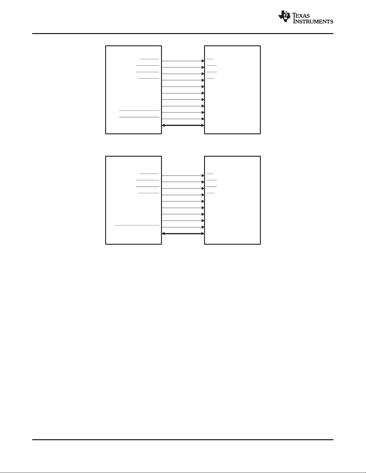
EMB_CS
EMB_CAS
EMB_RAS
EMB_WE
EMB_CLK
EMB_SDCKE
EMB_BA[1:0]
EMB_A[11:0]
EMB_WE_DQM[3:0]
EMB_D[31:0]
EMIFB
CE
CAS
RAS
WE
CLK
CKE
BA[1:0]
A[11:0]
DQM[3:0]
DQ[31:0]
SDRAM
2Mx32x4
Bank
EMB_CS
EMB_CAS
EMB_RAS
EMB_WE
EMB_CLK
EMB_SDCKE
EMB_BA[1:0]
EMB_A[11:0]
EMB_WE_DQM[0]
EMB_WE_DQM[1]
EMB_D[15:0]
EMIFB
CE
CAS
RAS
WE
CLK
CKE
BA[1:0]
A[11:0]
LDQM
UDQM
DQ[15:0]
SDRAM
2Mx16x4
Bank
TMS320C6745, TMS320C6747
SPRS377F –SEPTEMBER 2008–REVISED JUNE 2014
Figure 6-21. EMIFB to 2M × 16 × 4 bank SDRAM Interface
www.ti.com
100
Peripheral Information and Electrical Specifications Copyright © 2008–2014, Texas Instruments Incorporated
Figure 6-22. EMIFB to 2M × 32 × 4 bank SDRAM Interface
Submit Documentation Feedback
Product Folder Links: TMS320C6745 TMS320C6747
 Loading...