

Page 1

www.ti.com
TMS320C6727, TMS320C6726, TMS320C6722
Floating-Point Digital Signal Processors
SPRS268E – MAY 2005 – REVISED JANUARY 2007
1 TMS320C6727, TMS320C6726, TMS320C6722 DSPs
1.1 Features
• C672x: 32-/64-Bit 300-MHz Floating-Point DSPs • Three Multichannel Audio Serial Ports
• Upgrades to C67x+ CPU From C67x™ DSP
Generation:
– 2X CPU Registers [64 General-Purpose]
– New Audio-Specific Instructions
– Compatible With the C67x CPU
• Enhanced Memory System
– 256K-Byte Unified Program/Data RAM
– 384K-Byte Unified Program/Data ROM
– Single-Cycle Data Access From CPU Options
– Large Program Cache (32K Byte) Supports
RAM, ROM, and External Memory
• External Memory Interface (EMIF) Supports
– 100-MHz SDRAM (16- or 32-Bit)
– Asynchronous NOR Flash, SRAM (8-,16-, or
32-Bit)
– NAND Flash (8- or 16-Bit)
• Enhanced I/O System
– High-Performance Crossbar Switch
– Dedicated McASP DMA Bus
– Deterministic I/O Performance
• dMAX (Dual Data Movement Accelerator)
Supports:
– 16 Independent Channels
– Concurrent Processing of Two Transfer
Requests
– 1-, 2-, and 3-Dimensional
Memory-to-Memory and
Memory-to-Peripheral Data Transfers
– Circular Addressing Where the Size of a Flatpack (TQFP) [RFP Suffix]
Circular Buffer (FIFO) is not Limited to 2
n
– Table-Based Multi-Tap Delay Read and
Write Transfers From/To a Circular Buffer
– Transmit/Receive Clocks up to 50 MHz
– Six Clock Zones and 16 Serial Data Pins
– Supports TDM, I2S, and Similar Formats
– DIT-Capable (McASP2)
• Universal Host-Port Interface (UHPI)
– 32-Bit-Wide Data Bus for High Bandwidth
– Muxed and Non-Muxed Address and Data
• Two 10-MHz SPI Ports With 3-, 4-, and 5-Pin
• Two Inter-Integrated Circuit (I2C) Ports
• Real-Time Interrupt Counter/Watchdog
• Oscillator- and Software-Controlled PLL
• Applications:
– Professional Audio
• Mixers
• Effects Boxes
• Audio Synthesis
• Instrument/Amp Modeling
• Audio Conferencing
• Audio Broadcast
• Audio Encoder
– Emerging Audio Applications
– Biometrics
– Medical
– Industrial
• Commercial or Extended Temperature
• 144-Pin, 0.5-mm, PowerPAD™ Thin Quad
• 256-Terminal, 1.0-mm, 16x16 Array Plastic Ball
Grid Array (PBGA) [GDH and ZDH Suffixes]
Please be aware that an important notice concerning availability, standard warranty, and use in critical applications of Texas
Instruments semiconductor products and disclaimers thereto appears at the end of this document.
C67x, PowerPAD, TMS320C6000, C6000, DSP/BIOS, XDS, TMS320 are trademarks of Texas Instruments.
Philips is a registered trademark of Koninklijki Philips Electronics N.V.
All trademarks are the property of their respective owners.
PRODUCTION DATA information is current as of publication date.
Products conform to specifications per the terms of the Texas
Instruments standard warranty. Production processing does not
necessarily include testing of all parameters.
Copyright © 2005–2007, Texas Instruments Incorporated
Page 2

www.ti.com
TMS320C6727, TMS320C6726, TMS320C6722
Floating-Point Digital Signal Processors
SPRS268E – MAY 2005 – REVISED JANUARY 2007
1.2 Description
The TMS320C672x is the next generation of Texas Instruments' C67x generation of high-performance
32-/64-bit floating-point digital signal processors. The TMS320C672x includes the TMS320C6727,
TMS320C6726, and TMS320C6722 devices.
Enhanced C67x+ CPU. The C67x+ CPU is an enhanced version of the C67x CPU used on the C671x
DSPs. It is compatible with the C67x CPU but offers significant improvements in speed, code density, and
floating-point performance per clock cycle. At 300 MHz, the CPU is capable of a maximum performance of
2400 MIPS/1800 MFLOPS by executing up to eight instructions (six of which are floating-point
instructions) in parallel each cycle. The CPU natively supports 32-bit fixed-point, 32-bit single-precision
floating-point, and 64-bit double-precision floating-point arithmetic.
Efficient Memory System. The memory controller maps the large on-chip 256K-byte RAM and 384K-byte
ROM as unified program/data memory. Development is simplified since there is no fixed division between
program and data memory size as on some other devices.
The memory controller supports single-cycle data accesses from the C67x+ CPU to the RAM and ROM.
Up to three parallel accesses to the internal RAM and ROM from three of the following four sources are
supported:
• Two 64-bit data accesses from the C67x+ CPU
• One 256-bit program fetch from the core and program cache
• One 32-bit data access from the peripheral system (either dMAX or UHPI)
(1)
The large (32K-byte) program cache translates to a high hit rate for most applications. This prevents most
program/data access conflicts to the on-chip memory. It also enables effective program execution from an
off-chip memory such as an SDRAM.
High-Performance Crossbar Switch. A high-performance crossbar switch acts as a central hub between
the different bus masters (CPU, dMAX, UHPI) and different targets (peripherals and memory). The
crossbar is partially connected; some connections are not supported (for example, UHPI-to-peripheral
connections).
Multiple transfers occur in parallel through the crossbar as long as there is no conflict between bus
masters for a particular target. When a conflict does occur, the arbitration is a simple and deterministic
fixed-priority scheme.
The dMAX is given highest-priority since it is responsible for the most time-critical I/O transfers, followed
next by the UHPI, and finally by the CPU.
dMAX Dual Data Movement Accelerator. The dMAX is a module designed to perform Data Movement
Acceleration. The Data Movement Accelerator (dMAX) controller handles user-programmed data transfers
between the internal data memory controller and the device peripherals on the C672x DSPs. The dMAX
allows movement of data to/from any addressable memory space including internal memory, peripherals,
and external memory.
The dMAX controller includes features such as the capability to perform three-dimensional data transfers
for advanced data sorting, and the capability to manage a section of the memory as a circular buffer/FIFO
with delay-tap based reading and writing of data. The dMAX controller is capable of concurrently
processing two transfer requests (provided that they are to/from different source/destinations).
External Memory Interface (EMIF) for Flexibility and Expansion. The external memory interface on the
C672x supports a single bank of SDRAM and a single bank of asynchronous memory. The EMIF data
width is 16 bits wide on the C6726 and C6722, and 32 bits wide on the C6727.
SDRAM support includes x16 and x32 SDRAM devices with 1, 2, or 4 banks.
The C6726 and C6722 support SDRAM devices up to 128M bits.
(1) Throughout the remainder of the document, TMS320C6727 (or C6727), TMS320C6726 (or C6726), and/or TMS320C6722 (or C6722)
will be referred to as TMS320C672x (or C672x).
TMS320C6727, TMS320C6726, TMS320C6722 DSPs2 Submit Documentation Feedback
Page 3

www.ti.com
TMS320C6727, TMS320C6726, TMS320C6722
Floating-Point Digital Signal Processors
SPRS268E – MAY 2005 – REVISED JANUARY 2007
The C6727 extends SDRAM support to 256M-bit and 512M-bit devices.
Asynchronous memory support is typically used to boot from a parallel non-multiplexed NOR flash device
that can be 8, 16, or 32 bits wide. Booting from larger flash devices than are natively supported by the
dedicated EMIF address lines is accomplished by using general-purpose I/O pins for upper address lines.
The asynchronous memory interface can also be configured to support 8- or 16-bit-wide NAND flash. It
includes a hardware ECC calculation (for single-bit errors) that can operate on blocks of data up to
512 bytes.
Universal Host-Port Interface (UHPI) for High-Speed Parallel I/O. The Universal Host-Port Interface
(UHPI) is a parallel interface through which an external host CPU can access memories on the DSP.
Three modes are supported by the C672x UHPI:
• Multiplexed Address/Data - Half-Word (16-bit-wide) Mode (similar to C6713)
• Multiplexed Address/Data - Full Word (32-bit-wide) Mode
• Non-Multiplexed Mode - 16-bit Address and 32-bit Data Bus
The UHPI can also be restricted to accessing a single page (64K bytes) of memory anywhere in the
address space of the C672x; this page can be changed, but only by the C672x CPU. This feature allows
the UHPI to be used for high-speed data transfers even in systems where security is an important
requirement.
The UHPI is only available on the C6727.
Multichannel Audio Serial Ports (McASP0, McASP1, and McASP2) - Up to 16 Stereo Channels I2S.
The multichannel audio serial port (McASP) seamlessly interfaces to CODECs, DACs, ADCs, and other
devices. It supports the ubiquitous IIS format as well as many variations of this format, including time
division multiplex (TDM) formats with up to 32 time slots.
Each McASP includes a transmit and receive section which may operate independently or synchronously;
furthermore, each section includes its own flexible clock generator and extensive error-checking logic.
As data passes through the McASP, it can be realigned so that the fixed-point representation used by the
application code can be independent of the representation used by the external devices without requiring
any CPU overhead to make the conversion.
The McASP is a configurable module and supports between 2 and 16 serial data pins. It also has the
option of supporting a Digital Interface Transmitter (DIT) mode with a full 384 bits of channel status and
user data memory.
McASP2 is not available on the C6722.
Inter-Integrated Circuit Serial Ports (I2C0, I2C1). The C672x includes two inter-integrated circuit (I2C)
serial ports. A typical application is to configure one I2C serial port as a slave to an external user-interface
microcontroller. The other I2C serial port may then be used by the C672x DSP to control external
peripheral devices, such as a CODEC or network controller, which are functionally peripherals of the DSP
device.
The two I2C serial ports are pin-multiplexed with the SPI0 serial port.
Serial Peripheral Interface Ports (SPI0, SPI1). As in the case of the I2C serial ports, the C672x DSP
also includes two serial peripheral interface (SPI) serial ports. This allows one SPI port to be configured as
a slave to control the DSP while the other SPI serial port is used by the DSP to control external
peripherals.
The SPI ports support a basic 3-pin mode as well as optional 4- and 5-pin modes. The optional pins
include a slave chip-select pin and an enable pin which implements handshaking automatically in
hardware for maximum SPI throughput.
The SPI0 port is pin-multiplexed with the two I2C serial ports (I2C0 and I2C1). The SPI1 serial port is
pin-multiplexed with five of the serial data pins from McASP0 and McASP1.
Submit Documentation Feedback TMS320C6727, TMS320C6726, TMS320C6722 DSPs 3
Page 4

www.ti.com
TMS320C6727, TMS320C6726, TMS320C6722
Floating-Point Digital Signal Processors
SPRS268E – MAY 2005 – REVISED JANUARY 2007
Real-Time Interrupt Timer (RTI). The real-time interrupt timer module includes:
• Two 32-bit counter/prescaler pairs
• Two input captures (tied to McASP direct memory access [DMA] events for sample rate measurement)
• Four compares with automatic update capability
• Digital Watchdog (optional) for enhanced system robustness
Clock Generation (PLL and OSC). The C672x DSP includes an on-chip oscillator that supports crystals
in the range of 12 MHz to 25 MHz. Alternatively, the clock can be provided externally through the CLKIN
pin.
The DSP includes a flexible, software-programmable phase-locked loop (PLL) clock generator. Three
different clock domains (SYSCLK1, SYSCLK2, and SYSCLK3) are generated by dividing down the PLL
output. SYSCLK1 is the clock used by the CPU, memory controller, and memories. SYSCLK2 is used by
the peripheral subsystem and dMAX. SYSCLK3 is used exclusively for the EMIF.
1.2.1 Device Compatibility
The TMS320C672x floating-point digital signal processors are based on the new C67x+ CPU. This core is
code-compatible with the C67x CPU core used on the TMS320C671x DSPs, but with significant
enhancements including additional floating-point instructions. See Section 2.2
4 TMS320C6727, TMS320C6726, TMS320C6722 DSPs Submit Documentation Feedback
Page 5
www.ti.com
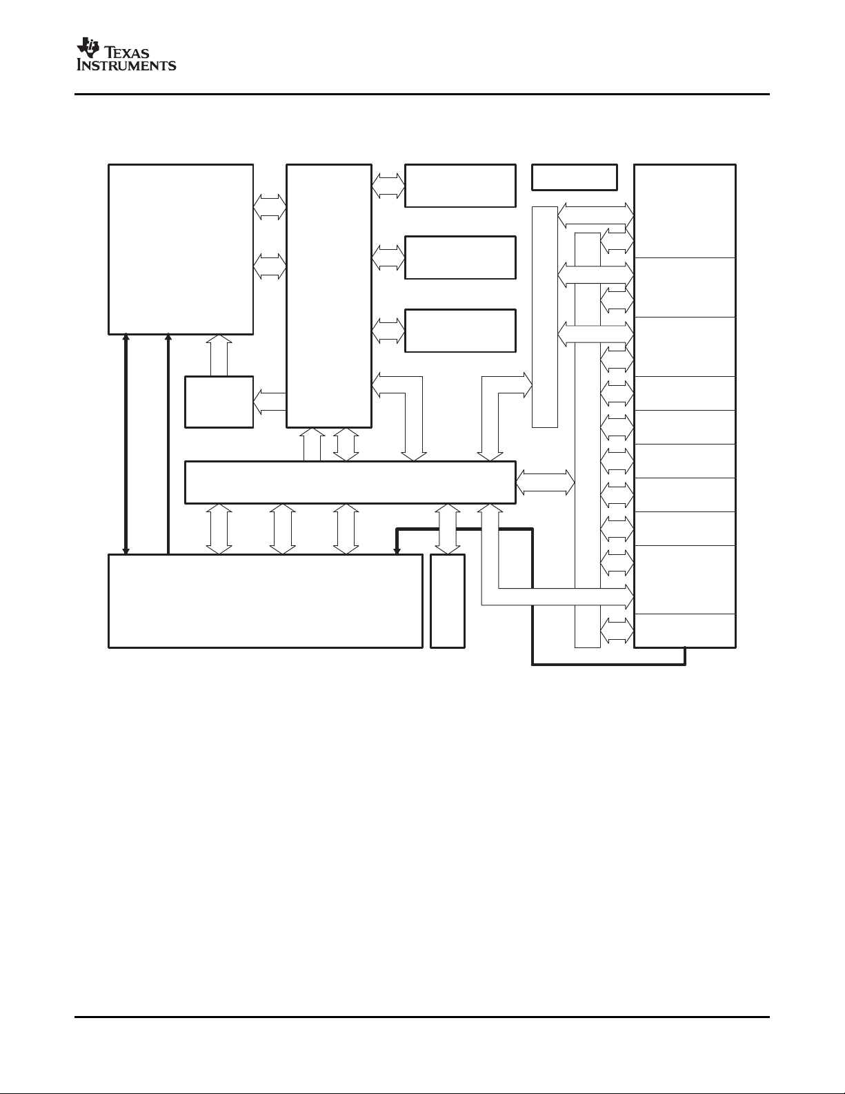
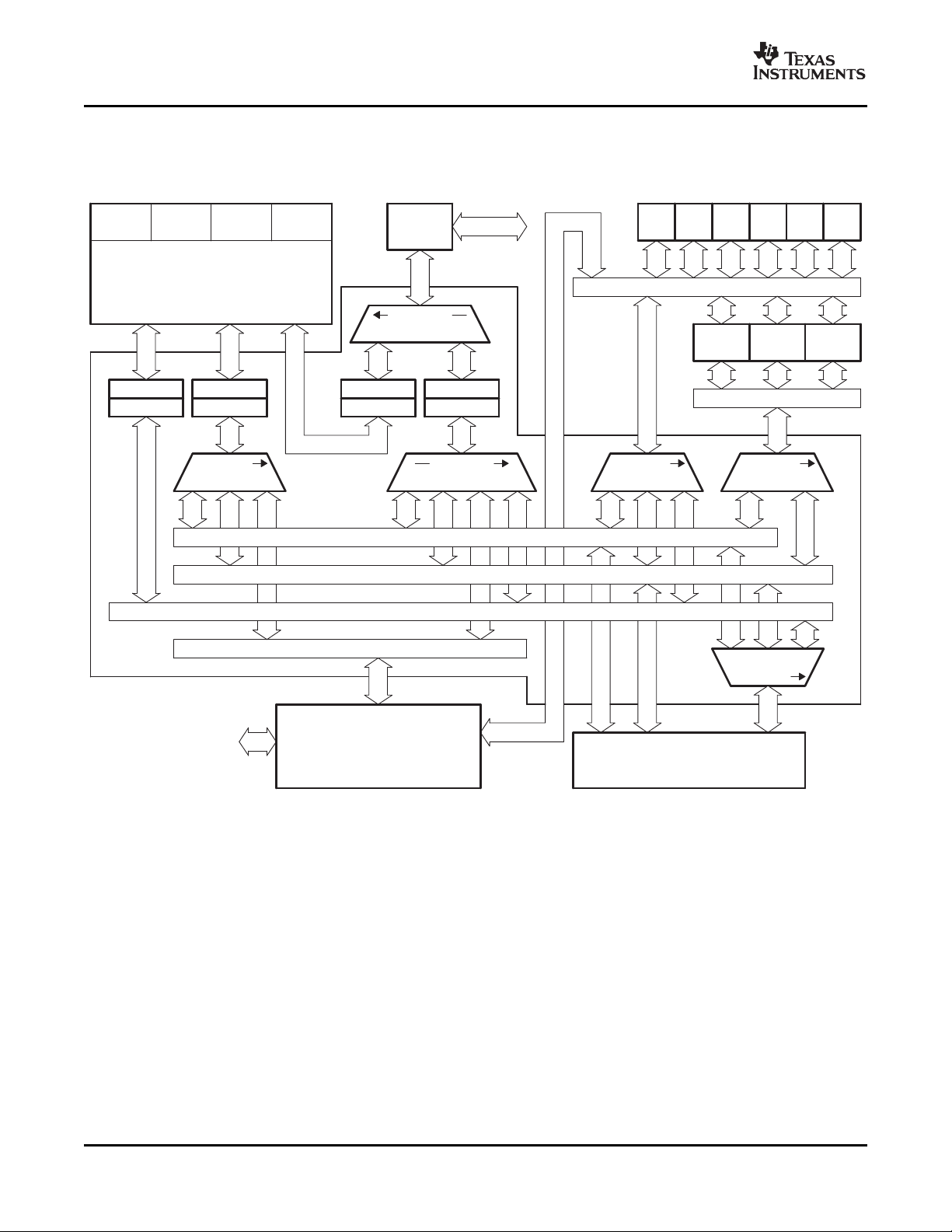
1.3 Functional Block Diagram
Program/Data
RAM
256K Bytes
256
256
Program/Data
ROM Page0
256K Bytes
256
Program/Data
ROM Page1
128K Bytes
3232
DMPPMP
CSP 32
256
32K Bytes
Program
Cache
64
D1
Data
R/W
R/W
DataD264
256
Program
FetchINTI/O
C67x+ CPU
Memory
Controller
32
High-Performance
Crossbar Switch
32
McASP DMA Bus
JTAG EMU
32
32
32
32
32
32
32
32
Peripheral Configuration Bus
EMIF
32
Events
In
32
MAX1MAX032CONTROL
32
Interrupts
Out
I/O
dMAX
McASP0
16 Serializers
McASP1
6 Serializers
McASP2
2 Serializers
+ DIT
SPI1
SPI0
I2C1
I2C0
RTI32
UHPI
PLL
Peripheral Interrupt and DMA Events
32
32
32
32
32
Figure 1-1 shows the functional block diagram of the C672x device.
TMS320C6727, TMS320C6726, TMS320C6722
Floating-Point Digital Signal Processors
SPRS268E – MAY 2005 – REVISED JANUARY 2007
A. UHPI is available only on the C6727. McASP2 is not available on the C6722.
Submit Documentation Feedback TMS320C6727, TMS320C6726, TMS320C6722 DSPs 5
Figure 1-1. C672x DSP Block Diagram
Page 6

www.ti.com
TMS320C6727, TMS320C6726, TMS320C6722
Floating-Point Digital Signal Processors
SPRS268E – MAY 2005 – REVISED JANUARY 2007
Contents
1 TMS320C6727, TMS320C6726, TMS320C6722 4.3 Recommended Operating Conditions ............... 33
DSPs ........................................................ 1
1.1 Features .............................................. 1
1.2 Description ............................................ 2
1.2.1 Device Compatibility ................................. 4
1.3 Functional Block Diagram ............................ 5
2 Device Overview ......................................... 7
2.1 Device Characteristics ................................ 7
2.2 Enhanced C67x+ CPU ............................... 8
2.3 CPU Interrupt Assignments ........................... 9
2.4 Internal Program/Data ROM and RAM .............. 10
2.5 Program Cache ...................................... 11
2.6 High-Performance Crossbar Switch ................. 12
2.7 Memory Map Summary ............................. 15
2.8 Boot Modes .......................................... 16
2.9 Pin Assignments .................................... 19
2.10 Development ........................................ 26
3 Device Configurations ................................. 30
3.1 Device Configuration Registers ..................... 30
3.2 Peripheral Pin Multiplexing Options ................. 30
3.3 Peripheral Pin Multiplexing Control ................. 31
4 Peripheral and Electrical Specifications ........... 33
4.1 Electrical Specifications ............................. 33
4.2 Absolute Maximum Ratings ......................... 33
4.4 Electrical Characteristics ............................ 34
4.5 Parameter Information .............................. 35
4.6 Timing Parameter Symbology ....................... 36
4.7 Power Supplies ...................................... 37
4.8 Reset ................................................ 38
4.9 Dual Data Movement Accelerator (dMAX) .......... 39
4.10 External Interrupts ................................... 44
4.11 External Memory Interface (EMIF) .................. 45
4.12 Universal Host-Port Interface (UHPI) [C6727 Only] . 55
4.13 Multichannel Audio Serial Ports (McASP0, McASP1,
and McASP2) ........................................ 68
4.14 Serial Peripheral Interface Ports (SPI0, SPI1) ...... 80
4.15 Inter-Integrated Circuit Serial Ports (I2C0, I2C1) ... 93
4.16 Real-Time Interrupt (RTI) Timer With Digital
Watchdog ............................................ 97
4.17 External Clock Input From Oscillator or CLKIN Pin 100
4.18 Phase-Locked Loop (PLL) ......................... 102
5 Application Example ................................. 105
6 Revision History ...................................... 106
7 Mechanical Data ....................................... 107
7.1 Package Thermal Resistance Characteristics ..... 107
7.2 Supplementary Information About the 144-Pin RFP
PowerPAD™ Package ............................. 108
7.3 Packaging Information ............................. 109
6 Contents Submit Documentation Feedback
Page 7

www.ti.com
TMS320C6727, TMS320C6726, TMS320C6722
Floating-Point Digital Signal Processors
SPRS268E – MAY 2005 – REVISED JANUARY 2007
2 Device Overview
2.1 Device Characteristics
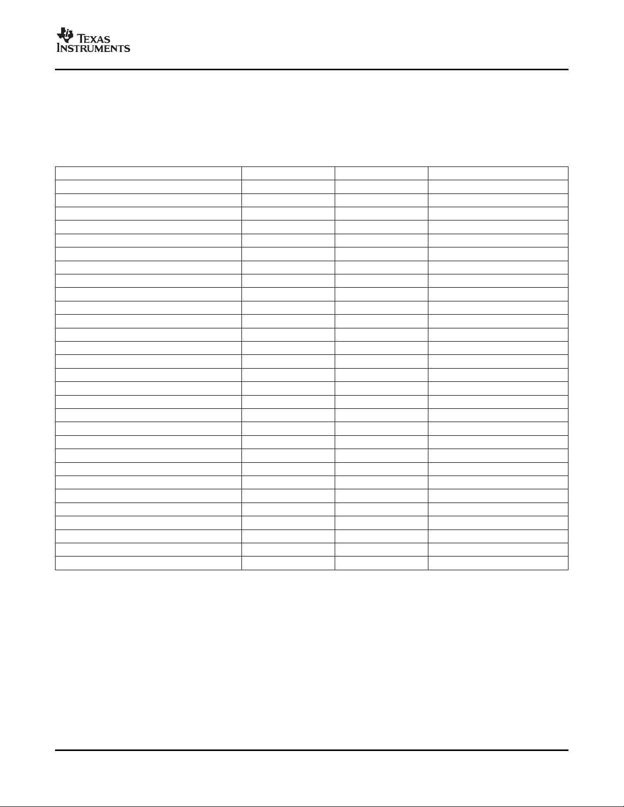
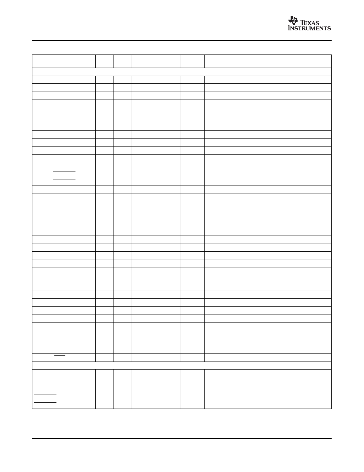
Table 2-1 provides an overview of the C672x DSPs. The table shows significant features of each device,
including the capacity of on-chip memory, the peripherals, the execution time, and the package type with
pin count.
Table 2-1. Characteristics of the C672x Processors
HARDWARE FEATURES C6727 C6726 C6722
dMAX 1
Peripherals
Not all peripheral pins are
available at the same time.
(For more details, see the
Device Configurations section.)
On-Chip Memory Size (KB) 256KB RAM 256KB RAM 128KB RAM
CPU ID + CPU Rev ID 0x0300
Frequency MHz 300, 250 250, 225 250, 225, 200
Cycle Time ns 4 ns (C6727A-250 and 4.4 ns (C6722A-225)
Voltage
Clock Generator Options Multiplier x4, x5, x6, ..., x25
Packages (see Section 7 )
Process Technology µm 0.13 µm
Product Status
(1) Advance Information concerns new products in the sampling or preproduction phase of development. Characteristic data and other
specifications are subject to change without notice.
(1)
EMIF 1 (32-bit) 1 (16-bit) 1 (16-bit)
UHPI 1 0 0
McASP 3 3 (McASP2 DIT only) 2
SPI 2
I2C 2
RTI 1
32KB Program Cache 32KB Program Cache 32KB Program Cache
384KB ROM 384KB ROM 384KB ROM
Control Status Register
(CSR.[31:16])
3.3 ns (C6727-300) 4 ns (C6722-250)
C6727-250) 5 ns (C6722-200)
Core (V) 1.2 V
I/O (V) 3.3 V
Prescaler /1, /2, /3, ..., /32
Postscaler /1, /2, /3, ..., /32
256-Terminal PBGA
17 x 17 mm – –
20 x 20 mm –
Product Preview (PP),
Advance Information (AI), or PD
Production Data (PD)
(GDH)
256-Terminal Green
PBGA (ZDH)
4 ns (C6726-250)
4.4 ns (C6726A-225)
144-Pin PowerPAD 144-Pin PowerPAD
Green TQFP (RFP) Green TQFP (RFP)
Submit Documentation Feedback Device Overview 7
Page 8
www.ti.com
.D1 .M1 .S1 .L1
Register File A
Data Path A
Cross
Paths
.D2 .M2 .S2 .L2
Register File B
Data Path B
TMS320C6727, TMS320C6726, TMS320C6722
Floating-Point Digital Signal Processors
SPRS268E – MAY 2005 – REVISED JANUARY 2007
2.2 Enhanced C67x+ CPU
The TMS320C672x floating-point digital signal processors are based on the new C67x+ CPU. This core is
code-compatible with the C67x CPU core used on the TMS320C671x DSPs, but with significant
enhancements including an increase in core operating frequency from 225 MHz to 300 MHz
operating at 1.2 V.
The CPU fetches 256-bit-wide advanced very-long instruction word (VLIW) fetch packets that are
composed of variable-length execute packets. The execute packets can supply from one to eight 32-bit
instructions to the eight functional units during every clock cycle. The variable-length execute packets are
a key memory-saving feature, distinguishing the C67x CPU from other VLIW architectures. Additionally,
execute packets can now span fetch packets, providing a code size improvement over the C67x CPU
core.
The CPU features two data paths, shown in Figure 2-1 , each composed of four functional units (.D, .M, .S,
and .L) and a register file. The .D unit in each data path is a data-addressing unit that is responsible for all
data transfers between the register files and the memory. The .M functional units are dedicated for
multiplies, and the .S and .L functional units perform a general set of arithmetic, logical, and branch
functions. All instructions operate on registers as opposed to data in memory, but results stored in the
32-bit registers can be subsequently moved to memory as bytes, half-words, or words.
(2)
while
The register file in each data path contains 32 32-bit registers for a total of 64 general-purpose registers.
This doubles the number of registers found on the C67x CPU core, allowing the optimizing C compiler to
pipeline more complex loops by decreasing register pressure significantly.
The four functional units in each data path of the CPU can freely share the 32 registers belonging to that
data path. Each data path also features a single cross path connected to the register file on the opposing
data path. This allows each data path to source one cross-path operand per cycle from the opposing
register file. On the C67x+ CPU, this single cross-path operand can be used by two functional units per
cycle, an improvement over the C67x CPU in which only one functional unit could use the cross-path
operand. In addition, the cross-path register read(s) are not counted as part of the limit of four reads of the
same register in a single cycle.
The C67x+ CPU executes all C67x instructions plus new floating-point instructions to improve
performance specifically during audio processing. These new instructions are listed in Table 2-2 .
(2) CPU speed is device-dependent. See Table 2-1 .
Figure 2-1. CPU Data Paths
8 Device Overview Submit Documentation Feedback
Page 9
www.ti.com
TMS320C6727, TMS320C6726, TMS320C6722
Floating-Point Digital Signal Processors
Table 2-2. New Floating-Point Instructions for C67x+ CPU
SPRS268E – MAY 2005 – REVISED JANUARY 2007
INSTRUCTION IMPROVES
MPYSPDP SP x DP → DP Faster than MPYDP.
MPYSP2DP SP x SP → DP Faster than MPYDP.
ADDSP (new to CPU “S” Unit) SP + SP → SP
ADDDP (new to CPU “S” Unit) DP + DP → DP
SUBSP (new to CPU “S” Unit) SP – SP → SP
SUBDP (new to CPU “S” Unit) DP – DP → DP
(1) SP means IEEE Single-Precision (32-bit) operations and DP means IEEE Double-Precision (64-bit) operations.
FLOATING-POINT
OPERATION
(1)
Improves high Q biquads (bass management) and FFT.
Improves Long FIRs (EQ).
Now up to four floating-point add and subtract operations in parallel.
Improves FFT performance and symmetric FIR.
Finally, two new registers, which are dedicated to communication with the dMAX unit, have been added to
the C67x+ CPU. These registers are the dMAX Event Trigger Register (DETR) and the dMAX Event
Status Register (DESR). They allow the CPU and dMAX to communicate without requiring any accesses
to the memory system.
2.3 CPU Interrupt Assignments
Table 2-3 lists the interrupt channel assignments on the C672x device. If more than one source is listed,
the interrupt channel is shared and an interrupt on this channel could have come from any of the enabled
peripherals on that channel.
The dMAX peripheral has two CPU interrupts dedicated to reporting FIFO status (INT7) and transfer
completion (INT8). In addition, the dMAX can generate interrupts to the CPU on lines INT9–13 and INT15
in response to peripheral events. To enable this functionality, the associated Event Entry within the dMAX
can be programmed so that a CPU interrupt is generated when the peripheral event is received.
Table 2-3. CPU Interrupt Assignments
CPU INTERRUPT INTERRUPT SOURCE
INT0 RESET
INT1 NMI (From dMAX or EMIF Interrupt)
INT2 Reserved
INT3 Reserved
INT4 RTI Interrupt 0
INT5 RTI Interrupts 1, 2, 3, and RTI Overflow Interrupts 0 and 1.
INT6 UHPI CPU Interrupt (from External Host MCU)
INT7 FIFO status notification from dMAX
INT8 Transfer completion notification from dMAX
INT9 dMAX event (0x2 specified in the dMAX interrupt event entry)
INT10 dMAX event (0x3 specified in the dMAX interrupt event entry)
INT11 dMAX event (0x4 specified in the dMAX interrupt event entry)
INT12 dMAX event (0x5 specified in the dMAX interrupt event entry)
INT13 dMAX event (0x6 specified in the dMAX interrupt event entry)
INT14 I2C0, I2C1, SPI0, SPI1 Interrupts
INT15 dMAX event (0x7 specified in the dMAX interrupt event entry)
Submit Documentation Feedback Device Overview 9
Page 10
www.ti.com
00 20
27072F2808
0F
3F
38
37
30
1F
18
10
17
3F
38
37
30
1F
18
17
10
2F
28
27
20
0F
08
00
07
Byte
ROM Page 1
Base Address
0x0004 0000
ROM Page 0
Base Address
0x0000 0000
Bank
0
Bank
1
Bank
2
Bank
3
13 33
10 30
17 37
14 34
1B 3B
18 38
1F 3F
1C 3C
RAM Page 0
Base Address
0x1000 0000
00 20
03 230704
27
24
0B
08
2B
28
0F
0C
2F
2C
Byte
Bank0Bank
1
Bank2Bank
3
Bank4Bank
5
Bank6Bank
7
TMS320C6727, TMS320C6726, TMS320C6722
Floating-Point Digital Signal Processors
SPRS268E – MAY 2005 – REVISED JANUARY 2007
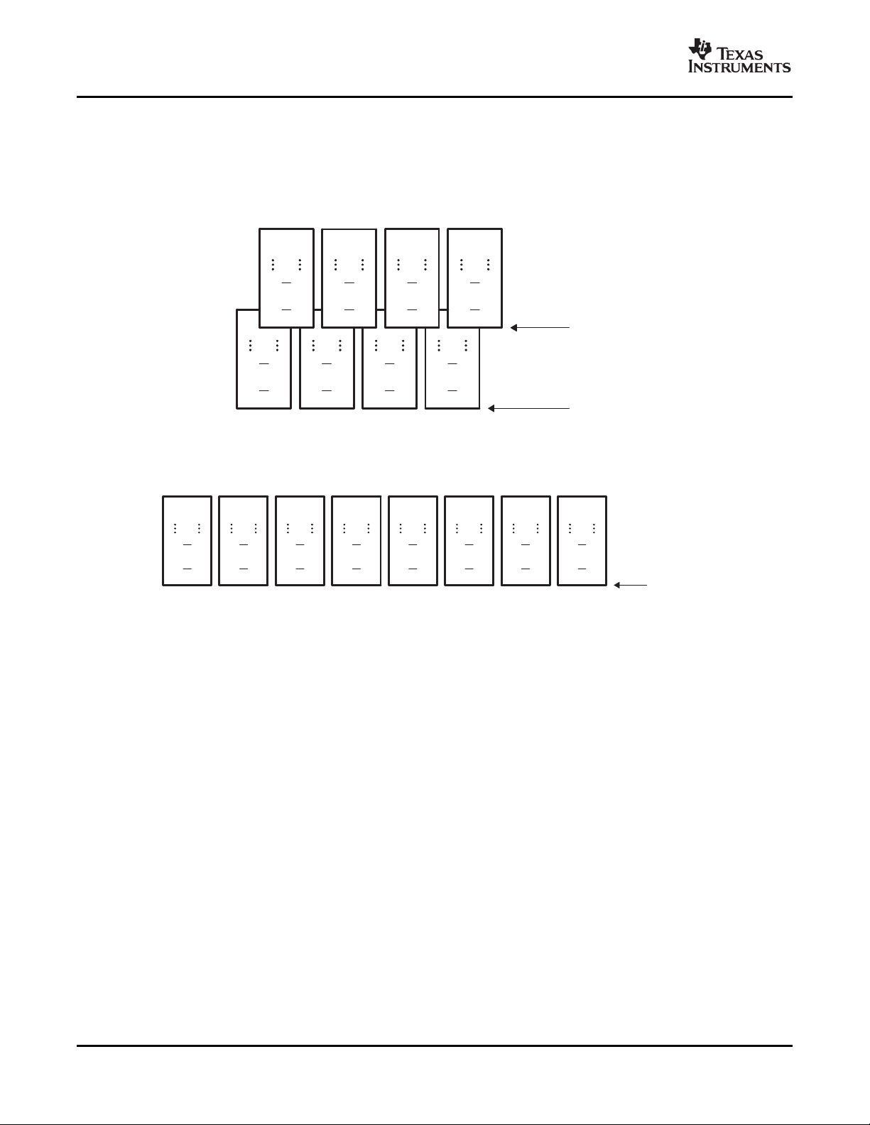
2.4 Internal Program/Data ROM and RAM
The organization of program/data ROM and RAM on C672x is simple and efficient. ROM is organized as
two 256-bit-wide pages with four 64-bit-wide banks. RAM is organized as a single 256-bit-wide page with
eight 32-bit-wide banks.
The internal memory organization is illustrated in Figure 2-2 (ROM) and Figure 2-3 (RAM).
Figure 2-2. Program/Data ROM Organization
Figure 2-3. Program/Data RAM Organization
The C672x memory controller supports up to three parallel accesses to the internal RAM and ROM from
three of the following four sources as long as there are no bank conflicts:
• Two 64-bit data accesses from the C67x+ CPU
• One 256-bit-wide program fetch from the program cache
• One 32-bit data access from the peripheral system (either dMAX or UHPI)
A program cache miss is 256 bits wide and conflicts only with data accesses to the same page. Multiple
data accesses to different pages, or to the same page but different banks will occur without conflict.
The organization of the C672x internal memory system into multiple pages (3 total) and a large number of
banks (16 total) means that it is straightforward to optimize DSP code to avoid data conflicts. Several
factors, including the large program cache and the partitioning of the memory system into multiple pages,
minimize the number of program versus data conflicts.
The result is an efficient memory system which allows easy tuning towards the maximum possible CPU
performance.
The C672x ROM consists of a software bootloader plus additional software. Please refer to the
C9230C100 TMS320C672x Floating-Point Digital Signal Processors ROM Data Manual (literature number
SPRS277) for more details on the ROM contents.
Device Overview10 Submit Documentation Feedback
Page 11
www.ti.com
2.5 Program Cache
The C672x DSP executes code directly from a large on-chip 32K-byte program cache. The program cache
has these key features:
• Wide 256-bit path to internal ROM/RAM
• Single-cycle access on cache hits
• 2-cycle miss penalty to internal ROM/RAM
• Caches external memory as well as ROM/RAM
• Direct-mapped
• Modes: Enable, Freeze, Bypass
• Software invalidate to support code overlay
The program cache line size is 256 bits wide and is matched with a 256-bit-wide path between cache and
internal memory. This allows the program cache to fill an entire line (corresponding to eight C67x+ CPU
instructions) with only a single miss penalty of 2 cycles.
The program cache control registers are listed in Table 2-4 .
TMS320C6727, TMS320C6726, TMS320C6722
Floating-Point Digital Signal Processors
SPRS268E – MAY 2005 – REVISED JANUARY 2007
Table 2-4. Program Cache Control Registers
REGISTER NAME BYTE ADDRESS DESCRIPTION
L1PISAR 0x2000 0000 L1P Invalidate Start Address
L1PICR 0x2000 0004 L1P Invalidate Control Register
CAUTION
Any application which modifies the contents of program RAM (for example, a program
overlay) must invalidate the addresses from program cache to maintain coherency by
explicitly writing to the L1PISAR and L1PICR registers.
The Cache Mode (Enable, Freeze, Bypass) is configured through a CPU internal register (CSR, bits 7:5).
These options are listed in Table 2-5 . Typically, only the Cache Enable Mode is used. But advanced users
may utilize Freeze and Bypass modes to tune performance.
Table 2-5. Cache Modes Set Through PCC Field of CSR CPU Register on C672x
CPU CSR[7:5] CACHE MODE
000b Enable (Deprecated - Means direct mapped RAM on some C6000 devices)
010b Enable - Cache is enabled, cache misses cause a line fill.
011b Freeze - Cache is enabled, but contents are unchanged by misses.
100b Bypass - Forces cache misses, cache contents frozen.
Other Values Reserved - Not Supported
CAUTION
Although the reset value of CSR[7:5] (PCC field) is 000b, the value may be modified
during the boot process by the ROM code. Refer to the appropriate ROM data sheet
for more details. However, note that the cache may be disabled when control is
actually passed to application code. Therefore, it may be necessary to write '010b' to
the PCC field to explicitly enable the cache at the start of application code.
CAUTION
Changing the cache mode through CSR[7:5] does not invalidate any lines already in
the cache. To invalidate the cache after modifications are made to program space, the
control registers L1PISAR and L1PICR must be used.
Submit Documentation Feedback Device Overview 11
Page 12
www.ti.com
SYSCLK3
SYSCLK1 SYSCLK2
SYSCLK3
BR3 BR4
2 1
Priority
EMIF
External
Memory
SDRAM/
Flash
Priority
21 3 4
T2
SYSCLK2
SYSCLK1
BR1
SYSCLK2
SYSCLK1
BR2
Program
Master
Port
(PMP)
CPU
Slave
Port
(CSP)
Data
Master
Port
(DMP)
Memory Controller
M1 T1 M2
Priority
1 2 3
PLL SPI0 I2C0 I2C1RTI SPI1
Peripheral Configuration Bus
McASP2McASP1McASP0
McASP DMA Bus
Priority
1 2 3
Priority
1 2
T4
T3
dMAX MAX0 Unit Master Port − High Priority
dMAX MAX1 Unit Master Port − Second Priority
Memory Controller DMP − Data Read/Write by CPU
UHPI Master Interface (External Host CPU)
UHPI
Universal Host-Port
Interface
M5
MAX0 MAX1
1 2 3
Priority
Config
dMAX
T5M3 M4
External
Host MCU
Config
ROM RAM CPU
Program
Cache
Crossbar
TMS320C6727, TMS320C6726, TMS320C6722
Floating-Point Digital Signal Processors
SPRS268E – MAY 2005 – REVISED JANUARY 2007
2.6 High-Performance Crossbar Switch
The C672x DSP includes a high-performance crossbar switch that acts as a central hub between bus
masters and targets. Figure 2-4 illustrates the connectivity of the crossbar switch.
As shown in Figure 2-4 , there are five bus masters:
Device Overview12 Submit Documentation Feedback
Figure 2-4. Block Diagram of Crossbar Switch
M1 Memory controller DMP for CPU data accesses to peripherals and EMIF.
M2 Memory controller PMP for program cache fills from the EMIF.
M3 dMAX HiMAX master port for high-priority DMA accesses.
M4 dMAX LoMAX master port for lower-priority DMA accesses.
M5 UHPI master port for an external MCU to access on-chip and off-chip memories.
Page 13
www.ti.com
TMS320C6727, TMS320C6726, TMS320C6722
Floating-Point Digital Signal Processors
SPRS268E – MAY 2005 – REVISED JANUARY 2007
The five bus masters arbitrate for five different target groups:
T1 On-chip memories through the CPU Slave Port (CSP).
T2 Memories on the external memory interface (EMIF).
T3 Peripheral registers through the peripheral configuration bus.
T4 McASP serializers through the dedicated McASP DMA bus.
T5 dMAX registers.
The crossbar switch supports parallel accesses from different bus masters to different targets. When two
or more bus masters contend for the same target beginning at the same cycle, then the highest-priority
master is given ownership of the target while the other master(s) are stalled. However, once ownership of
the target is given to a bus master, it is allowed to complete its access before ownership is arbitrated
again. Following are two examples.
Example 1: Simultaneous accesses without conflict
• dMAX HiMAX accesses McASP Data Port for transfer of audio data.
• dMAX LoMAX accesses SPI port for control processing.
• UHPI accesses internal RAM through the CSP.
• CPU fills program cache from EMIF.
Example 2: Conflict over a shared resource
• dMAX HiMAX accesses RTI port for McASP sample rate measurement.
• dMAX LoMAX accesses SPI port for control processing.
In Example 2, both masters contend for the same target, the peripheral configuration bus. The HiMAX
access will be given priority over the LoMAX access.
The master priority is illustrated in Figure 2-4 by the numbers 1 through 4 in the bus arbiter symbols. Note
that the EMIF arbitration is distributed so that only one bridge crossing is necessary for PMP accesses.
The effect is that PMP has 5th priority to the EMIF but lower latency.
A bus bridge is needed between masters and targets which run at different clock rates. The bus bridge
contains a small FIFO to allow the bridge to accept an incoming (burst) access at one clock rate and pass
it through the bridge to a target running at a different rate. Table 2-6 lists the FIFO properties of the four
bridges (BR1, BR2, BR3, and BR4) in Figure 2-4 .
Table 2-6. Bus Bridges
LABEL BRIDGE DESCRIPTION MASTER CLOCK TARGET CLOCK
BR1 DMP Bridge to peripherals, dMAX, EMIF SYSCLK1 SYSCLK2
BR2 dMAX, UHPI to ROM/RAM (CSP) SYSCLK2 SYSCLK1
BR3 PMP to EMIF SYSCLK1 SYSCLK3
BR4 CPU, UHPI, and dMAX to EMIF SYSCLK2 SYSCLK3
Submit Documentation Feedback Device Overview 13
Page 14
www.ti.com
TMS320C6727, TMS320C6726, TMS320C6722
Floating-Point Digital Signal Processors
SPRS268E – MAY 2005 – REVISED JANUARY 2007
Figure 2-5 shows the bit layout of the device-level bridge control register (CFGBRIDGE) and Table 2-7
contains a description of the bits.
31 16
Reserved
15 1 0
Reserved CSPRST
LEGEND: R/W = Read/Write; R = Read only; - n = value after reset
Figure 2-5. CFGBRIDGE Register Bit Layout (0x4000 0024)
Table 2-7. CFGBRIDGE Register Bit Field Description (0x4000 0024)
BIT NO. NAME RESET VALUE READ WRITE DESCRIPTION
31:1 Reserved N/A N/A Reads are indeterminate. Only 0s should be written to these bits.
0 CSPRST 1 R/W Resets the CSP Bridge (BR2 in Figure 2-4 ).
1 = Bridge Reset Asserted
0 = Bridge Reset Released
CAUTION
The CSPRST bit must be asserted after any change to the PLL that affects SYSCLK1
and SYSCLK2 and must be released before any accesses to the CSP bridge occur
from either the dMAX or the UHPI.
R/W, 1
14 Device Overview Submit Documentation Feedback
Page 15
www.ti.com
TMS320C6727, TMS320C6726, TMS320C6722
Floating-Point Digital Signal Processors
SPRS268E – MAY 2005 – REVISED JANUARY 2007
2.7 Memory Map Summary
A high-level memory map of the C672x DSP appears in Table 2-8 . The base address of each region is
listed. Any address past the end address must not be read or written. The table also lists whether the
regions are word-addressable or byte- and word-addressable.
Table 2-8. C672x Memory Map
DESCRIPTION BASE ADDRESS END ADDRESS BYTE- OR WORD-ADDRESSABLE
Internal ROM Page 0 (256K Bytes) 0x0000 0000 0x0003 FFFF Byte and Word
Internal ROM Page 1 (128K Bytes) 0x0004 0000 0x0005 FFFF Byte and Word
Internal RAM Page 0 (256K Bytes) 0x1000 0000 0x1003 FFFF Byte and Word
Memory and Cache Control Registers 0x2000 0000 0x2000 001F Word Only
Emulation Control Registers (Do Not Access) 0x3000 0000 0x3FFF FFFF Word Only
Device Configuration Registers 0x4000 0000 0x4000 0083 Word Only
PLL Control Registers 0x4100 0000 0x4100 015F Word Only
Real-time Interrupt (RTI) Control Registers 0x4200 0000 0x4200 00A3 Word Only
Universal Host-Port Interface (UHPI) Registers 0x4300 0000 0x4300 0043 Word Only
McASP0 Control Registers 0x4400 0000 0x4400 02BF Word Only
McASP1 Control Registers 0x4500 0000 0x4500 02BF Word Only
McASP2 Control Registers 0x4600 0000 0x4600 02BF Word Only
SPI0 Control Registers 0x4700 0000 0x4700 007F Word Only
SPI1 Control Registers 0x4800 0000 0x4800 007F Word Only
I2C0 Control Registers 0x4900 0000 0x4900 007F Word Only
I2C1 Control Registers 0x4A00 0000 0x4A00 007F Word Only
McASP0 DMA Port (any address in this range) 0x5400 0000 0x54FF FFFF Word Only
McASP1 DMA Port (any address in this range) 0x5500 0000 0x55FF FFFF Word Only
McASP2 DMA Port (any address in this range) 0x5600 0000 0x56FF FFFF Word Only
dMAX Control Registers 0x6000 0000 0x6000 008F Word Only
MAX0 (HiMAX) Event Entry Table 0x6100 8000 0x6100 807F Byte and Word
Reserved 0x6100 8080 0x6100 809F
MAX0 (HiMAX) Transfer Entry Table 0x6100 80A0 0x6100 81FF Byte and Word
MAX1 (LoMAX) Event Entry Table 0x6200 8000 0x6200 807F Byte and Word
Reserved 0x6200 8080 0x6200 809F
MAX1 (LoMAX) Transfer Entry Table 0x6200 80A0 0x6200 81FF Byte and Word
External SDRAM space on EMIF 0x8000 0000 0x8FFF FFFF Byte and Word
External Asynchronous / Flash space on EMIF 0x9000 0000 0x9FFF FFFF Byte and Word
EMIF Control Registers 0xF000 0000 0xF000 00BF Word Only
(1) The upper byte of the EMIF’s SDRAM Configuration Register (SDCR[31:24]) is byte-addressable to support placing the EMIF into the
Self-Refresh State without triggering the SDRAM Initialization Sequence.
(1)
Submit Documentation Feedback Device Overview 15
Page 16
www.ti.com
TMS320C6727, TMS320C6726, TMS320C6722
Floating-Point Digital Signal Processors
SPRS268E – MAY 2005 – REVISED JANUARY 2007
2.8 Boot Modes
The C672x DSP supports only one hardware bootmode option, this is to boot from the internal ROM
starting at address 0x0000 0000. Other bootmode options are implemented by a software bootloader
stored in ROM. The software bootloader uses the CFGPIN0 and CFGPIN1 registers, which capture the
state of various device pins at reset, to determine which mode to enter. Note that in practice, only a few
pins are used by the software.
Only an externally applied RESET causes the CFGPIN0 and CFGPIN1 registers to
recapture their associated pin values. Neither an emulator reset nor a RTI reset
causes these registers to update.
The ROM bootmodes include:
• Parallel Flash on EM_CS[2]
• SPI0 or I2C1 master mode from serial EEPROM
• SPI0 or I2C1 slave mode from external MCU
• UHPI from an external MCU
Table 2-9 describes the required boot pin settings at device reset for each bootmode.
CAUTION
Table 2-9. Required Boot Pin Settings at Device Reset
BOOT MODE UHPI_HCS SPI0_SOMI SPI0_SIMO SPI0_CLK
UHPI 0 BYTEAD
Parallel Flash 1 0 1 0
SPI0 Master 1 0 0 1
SPI0 Slave 1 0 1 1
I2C1 Master 1 1 0 1
I2C1 Slave 1 1 1 1
(1) When UHPI_HCS is 0, the state of the SPI0_SOMI, SPI0_SIMO, and SPI0_CLK pins is copied into the specified bits in the CFGHPI
register described in Table 4-12 .
(1)
(1)
FULL
Refer to the C9230C100 TMS320C672x Floating-Point Digital Signal Processor ROM Data Manual
(literature number SPRS277) for details on supported bootmodes and their implementation.
(1)
NMUX
Device Overview16 Submit Documentation Feedback
Page 17
www.ti.com
TMS320C6727, TMS320C6726, TMS320C6722
Floating-Point Digital Signal Processors
SPRS268E – MAY 2005 – REVISED JANUARY 2007
Figure 2-6 shows the bit layout of the CFGPIN0 register and Table 2-10 contains a description of the bits.
31 8
Reserved
7 6 5 4 3 2 1 0
PINCAP7 PINCAP6 PINCAP5 PINCAP4 PINCAP3 PINCAP2 PINCAP1 PINCAP0
LEGEND: R/W = Read/Write; R = Read only; - n = value after reset
Figure 2-6. CFGPIN0 Register Bit Layout (0x4000 0000)
Table 2-10. CFGPIN0 Register Bit Field Description (0x4000 0000)
BIT NO. NAME DESCRIPTION
31:8 Reserved Reads are indeterminate. Only 0s should be written to these bits.
7 PINCAP7 SPI0_SOMI/I2C0_SDA pin state captured on rising edge of RESET pin.
6 PINCAP6 SPI0_SIMO pin state captured on rising edge of RESET pin.
5 PINCAP5 SPI0_CLK/I2C0_SCL pin state captured on rising edge of RESET pin.
4 PINCAP4 SPI0_SCS/I2C1_SCL pin state captured on rising edge of RESET pin.
3 PINCAP3 SPI0_ENA/I2C1_SDA pin state captured on rising edge of RESET pin.
2 PINCAP2 AXR0[8]/AXR1[5]/SPI1_SOMI pin state captured on rising edge of RESET pin.
1 PINCAP1 AXR0[9]/AXR1[4]/SPI1_SIMO pin state captured on rising edge of RESET pin.
0 PINCAP0 AXR0[7]/SPI1_CLK pin state captured on rising edge of RESET pin.
Submit Documentation Feedback Device Overview 17
Page 18

www.ti.com
TMS320C6727, TMS320C6726, TMS320C6722
Floating-Point Digital Signal Processors
SPRS268E – MAY 2005 – REVISED JANUARY 2007
Figure 2-7 shows the bit layout of the CFGPIN1 register and Table 2-11 contains a description of the bits.
31 8
Reserved
7 6 5 4 3 2 1 0
PINCAP15 PINCAP14 PINCAP13 PINCAP12 PINCAP11 PINCAP10 PINCAP9 PINCAP8
LEGEND: R/W = Read/Write; R = Read only; - n = value after reset
Figure 2-7. CFGPIN1 Register Bit Layout (0x4000 0004)
Table 2-11. CFGPIN1 Register Bit Field Description (0x4000 0004)
BIT NO. NAME DESCRIPTION
31:8 Reserved Reads are indeterminate. Only 0s should be written to these bits.
7 PINCAP15 AXR0[5]/ SPI1_SCS pin state captured on rising edge of RESET pin.
6 PINCAP14 AXR0[6]/ SPI1_ENA pin state captured on rising edge of RESET pin.
5 PINCAP13 UHPI_HCS pin state captured on rising edge of RESET pin.
4 PINCAP12 UHPI_HD[0] pin state captured on rising edge of RESET pin.
3 PINCAP11 EM_D[16]/UHPI_HA[0] pin state captured on rising edge of RESET pin.
2 PINCAP10 AFSX0 pin state captured on rising edge of RESET pin.
1 PINCAP9 AFSR0 pin state captured on rising edge of RESET pin.
0 PINCAP8 AXR0[0] pin state captured on rising edge of RESET pin.
Device Overview18 Submit Documentation Feedback
Page 19
www.ti.com
2.9 Pin Assignments
SPI0_ENA
/I2C1_
SDA
SPI0_CLK
/I2C0_
SCL
DV
DD
V
SS
EM_RW
EM_RAS
V
SS
EM_BA[1]
EM_A[0]
V
SS
EM_A[3]
EM_A[5]
EM_A[7]
EM_A[9]
DV
DD
V
SS
DV
DD
EM_WE_
DQM[3]
EM_A[11]
EM_A[8]
EM_A[6]
EM_A[4]
EM_A[2]
EM_A[1]
EM_A[10]
EM_BA[0]
EM_CS[0]
EM_CS[2]
EM_OE
/I2C1_
SPI0_SCS
SCL
SIMO
SPI0_
DV
DD
AXR0[0]
SPI0_
SOMI
/I2C0_
SDA
AHCLKR2
EM_WAIT
UHPI_
HD[8]
HD[9]
UHPI_
HD[11]
UHPI_
HD[13]
UHPI_
DV
DD
HD[1]
UHPI_
UHPI_
HD[4]
HD[2]
UHPI_
HD[6]
UHPI_
HD[7]
UHPI_
EM_CLK
EM_CKE
DQM[1]
EM_WE_
EM_D[8]
DQM[2]
EM_WE_
HD[5]
UHPI_
DV
DD
HD[3]
UHPI_
HD[0]
UHPI_
UHPI_
HD[15]
UHPI_
HD[14]
HD[12]
UHPI_
HD[10]
UHPI_
DV
DD
DV
DD
ACLKR2
AXR0[1]
AXR0[2]AXR0[4]
AXR0[3]
AFSR2
DV
DD
V
SS
V
SS
CV
DD
CV
DD
CV
DD
CV
DD
V
SS
V
SS
DV
DD
EM_A[12]
EM_D[10]
EM_D[9]EM_D[11]
EM_D[12]
EM_D[24]
/UHPI_
HA[8]
HA[9]
EM_D[25]
/UHPI_
CV
DD
V
SS
V
SS
V
SS
V
SS
V
SS
V
SS
CV
DD
ACLKX2
AFSX2
/SPI1_
AXR0[5]
SCS
AXR0[6]
/SPI1_
ENA
V
SS
AXR0[7]
/SPI1_
CLK
HCNTL[1]
UHPI_
HINT
AMUTE2/
CV
DD
V
SS
V
SS
V
SS
V
SS
V
SS
V
SS
CV
DD
/UHPI_
HA[11]
EM_D[27]
HA[10]
EM_D[26]
/UHPI_
EM_D[13]
V
SS
EM_D[14]
EM_D[1]
EM_D[0]
EM_D[15]
DV
DD
HA[12]
EM_D[28]
/UHPI_
HA[13]
EM_D[29]
/UHPI_
V
SS
V
SS
V
SS
V
SS
V
SS
CV
DD
V
SS
CV
DD
/UHPI_
HA[14]
EM_D[30]
V
SS
CV
DD
CV
DD
V
SS
CV
DD
V
SS
V
SS
V
SS
V
SS
V
SS
V
SS
V
SS
V
SS
V
SS
V
SS
V
SS
V
SS
V
SS
CV
DD
V
SS
CV
DD
V
SS
CV
DD
V
SS
V
SS
V
SS
CV
DD
CV
DD
CV
DD
CV
DD
V
SS
V
SS
DV
DD
DV
DD
DV
DD
DV
DD
DV
DD
V
SS
EM_D[2]
HA[0]
EM_D[16]
/UHPI_
HA[15]
EM_D[31]
/UHPI_
EM_D[3]
EM_D[4]
HA[1]
EM_D[17]
/UHPI_
HA[2]
EM_D[18]
/UHPI_
EM_D[5]
EM_D[6]
HA[3]
EM_D[19]
/UHPI_
EM_D[7]
EM_WE_
DQM[0]
HA[4]
EM_D[20]
/UHPI_
HA[6]
EM_D[22]
/UHPI_
HD[29]
UHPI_
TRST
OSCV
DD
HD[31]
UHPI_
HD[18]
UHPI_
UHPI_
HD[20]
HRDY
UHPI_
HDS[1]
UHPI_
HRW
UHPI_
HCNTL[0]
UHPI_
HBE[2]
UHPI_
HBE[1]
UHPI_
HBE[0]
UHPI_
HDS[2]
UHPI_
HCS
UHPI_
HAS
UHPI_
AXR0[8]
/AXR1[5]
/SPI1_
SOMI
SIMO
/SPI1_
/AXR1[4]
AXR0[9]
/AXR1[3]
AXR0[10]
/AXR1[2]
AXR0[11]
/AXR1[1]
AXR0[12]
V
SS
/AXR2[1]
AXR0[14]
/AXR1[0]
AXR0[13]
/AXR2[0]
AXR0[15]
ACLKR0
AFSR0
ACLKX0
EM_WE
EM_CAS
HA[5]
EM_D[21]
/UHPI_
HD[26]
UHPI_
HD[27]
UHPI_
HD[28]
UHPI_
TMS
OSCOUT
V
SS
UHPI_
HD[17]
HD[19]
UHPI_
HD[21]
UHPI_
HD[22]
UHPI_
HD[23]
UHPI_
/AHCLKR1
AHCLKR0
AFSX0
DV
DD
DV
DD
DV
DD
V
SS
V
SS
DV
DD
HBE[3]
UHPI_
/AHCLKX2
AHCLKX0
AMUTE1
ACLKX1
AFSX1
RESET
CLKIN
OSCIN
PLLHV
HD[30]
UHPI_
TDO
HD[25]
UHPI_
HD[24]
UHPI_
HA[7]
EM_D[23]
/UHPI_
TCK
EMU[1]
EMU[0]
TDI
V
SS
OSCV
SS
HD[16]
/HHWIL
UHPI_
V
SS
AFSR1
ACLKR1
AHCLKX1
AMUTE0
T
R
P
N
M
L
K
J
H
G
F
E
D
C
B
A
1 2 3 4 5 6 7 8 9 10 11 12 13 14 15 16
2.9.1 Pin Maps
TMS320C6727, TMS320C6726, TMS320C6722
Floating-Point Digital Signal Processors
SPRS268E – MAY 2005 – REVISED JANUARY 2007
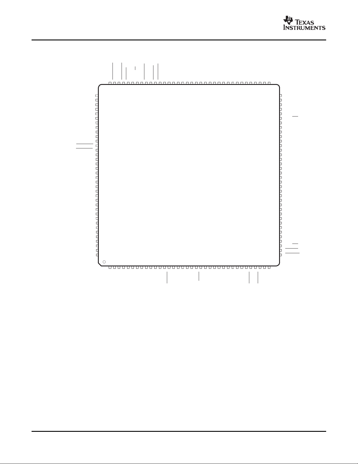
Figure 2-8 and Figure 2-9 show the pin assignments on the 256-terminal GDH/ZDH package and the
144-pin RFP package, respectively.
Submit Documentation Feedback Device Overview 19
Figure 2-8. 256-Terminal Ball Grid Array (GDH/ZDH Suffix)—Bottom View
Page 20
www.ti.com
78
EM_A[7]
109
1
108
72
2 107
3 106
4 105
5 104
6 103
7 102
8 101
9 100
10 99
11 98
12 97
13 96
14 95
15 94
16 93
17 92
18 91
19 90
20 89
21 88
22 87
23 86
24 85
25 84
26 83
27 82
28 81
29 80
30 79
31
32 77
33 76
34 75
35 74
36 73
110 71
111 70
112 69
113 68
114 67
115 66
116 65
117 64
118 63
119 62
120 61
121 60
122 59
123 58
124
57
125 56
126 55
127 54
128 53
129 52
130 51
131 50
132 49
133 48
134 47
135 46
136 45
137 44
138 43
139 42
140 41
141 40
142 39
143 38
37144
V
SS
AHCLKX0/AHCLKX2
AMUTE0
AMUTE1
AHCLKX1
V
SS
ACLKX1
CV
DD
ACLKR1
DV
DD
AFSX1
AFSR1
V
SS
RESET
V
SS
CV
DD
CLKIN
V
SS
TMS
CV
DD
TRST
OSCV
SS
OSCIN
OSCOUT
OSCV
DD
V
SS
PLLHV
TDI
TDO
V
SS
DV
DD
EMU[0]
CV
DD
EMU[1]
TCK
V
SS
SPI0_CLK/I2C0_SCL
SPI0_SCS/I2C1_SCL
V
SS
SPI0_ENA/I2C1_SDA
EM_OE
DV
DD
EM_RW
CV
DD
EM_CS[2]
V
SS
EM_RAS
EM_CS[0]
EM_BA[0]
V
SS
EM_BA[1]
EM_A[10]
DV
DD
EM_A[0]
CV
DD
EM_A[1]
EM_A[2]
V
SS
EM_A[3]
CV
DD
EM_A[4]
EM_A[5]
V
SS
DV
DD
EM_A[6]
V
SS
CV
DD
EM_A[8]
EM_A[9]
EM_A[11]
DV
DD
V
SS
SPI0_SIMO
SPI0_SOMI/I2C0_SDA
DV
DD
AXR0[0]
V
SS
AXR0[1]
AXR0[2]
AXR0[3]
V
SS
AXR0[4]
AXR0[5]/SPI1_SCS
AXR0[6]/SPI1_ENA
AXR0[7]/SPI1_CLK
CV
DD
V
SS
DV
DD
AXR0[8]/AXR1[5]/SPI1_SOMI
AXR0[9]/AXR1[4]/SPI1_SIMO
CV
DD
V
SS
AXR0[10]/AXR1[3]
AXR0[11]/AXR1[2]
CV
DD
V
SS
AXR0[12]/AXR1[1]
AXR0[13]/AXR1[0]
DV
DD
AXR0[14]/AXR2[1]
AXR0[15]/AXR2[0]
ACLKR0
V
SS
AFSR0
ACLKX0
AHCLKR0/AHCLKR1
AFSX0
V
SS
EM_CLK
EM_CKE
V
SS
DV
DD
EM_WE_DQM[1]
EM_D[8]
CV
DD
EM_D[9]
EM_D[10]
V
SS
EM_D[11]
DV
DD
EM_D[12]
EM_D[13]
CV
DD
EM_D[14]
EM_D[15]
V
SS
CV
DD
EM_D[0]
EM_D[1]
DV
DD
EM_D[2]
EM_D[3]
V
SS
EM_D[4]
EM_D[5]
CV
DD
EM_D[6]
DV
DD
EM_D[7]
V
SS
EM_WE_DQM[0]
EM_WE
EM_CAS
TMS320C6727, TMS320C6726, TMS320C6722
Floating-Point Digital Signal Processors
SPRS268E – MAY 2005 – REVISED JANUARY 2007
A. Actual size of Thermal Pad is 5.4 mm × 5.4 mm. See Section 7.3 .
Figure 2-9. 144-Pin Low-Profile Quad Flatpack (RFP Suffix)—Top View
20 Device Overview Submit Documentation Feedback
Page 21
www.ti.com
2.9.2 Terminal Functions
TMS320C6727, TMS320C6726, TMS320C6722
Floating-Point Digital Signal Processors
SPRS268E – MAY 2005 – REVISED JANUARY 2007
Table 2-12 , the Terminal Functions table, identifies the external signal names, the associated pin/ball
numbers along with the mechanical package designator, the pin type (I, O, IO, OZ, or PWR), whether the
pin/ball has any internal pullup/pulldown resistors, whether the pin/ball is configurable as an IO in GPIO
mode, and a functional pin description.
Table 2-12. Terminal Functions
SIGNAL NAME RFP TYPE
EM_A[0] 91 J16 O - N
EM_A[1] 89 J15 O - N
EM_A[2] 88 K15 O - N
EM_A[3] 86 L16 O - N
EM_A[4] 84 L15 O - N
EM_A[5] 83 M16 O - N
EM_A[6] 80 M15 O - N EMIF Address Bus
EM_A[7] 79 N16 O - N
EM_A[8] 76 N15 O - N
EM_A[9] 75 P16 O - N
EM_A[10] 93 H15 O - N
EM_A[11] 74 P15 O - N
EM_A[12] - P12 O IPD N
EM_BA[0] 96 G15 O - N
EM_BA[1] 94 H16 O - N
EM_CS[0] 97 F15 O - N SDRAM Chip Select
EM_CS[2] 100 E15 O - N Asynchronous Memory Chip Select
EM_CAS 37 R3 O - N SDRAM Column Address Strobe
EM_RAS 98 F16 O - N SDRAM Row Address Strobe
EM_WE 38 T3 O - N SDRAM/Asynchronous Write Enable
EM_CKE 71 T14 O - N SDRAM Clock Enable
EM_CLK 70 R14 O - N EMIF Output Clock
EM_ WE_DQM[0] 39 R4 O - N Write Enable or Byte Enable for EM_D[7:0]
EM_ WE_DQM[1] 67 T13 O - N Write Enable or Byte Enable for EM_D[15:8]
EM_ WE_DQM[2] - P13 O IPU N Write Enable or Byte Enable for EM_D[23:16]
EM_ WE_DQM[3] - R15 O IPU N Write Enable or Byte Enable for EM_D[31:24]
EM_OE 104 D15 O - N SDRAM/Asynchronous Output Enable
EM_R W 102 E16 O - N Asynchronous Memory Read/not Write
EM_WAIT - D14 I IPU N
(1) TYPE column refers to pin direction in functional mode. If a pin has more than one function with different directions, the functions are
separated with a slash (/).
(2) PULL column:
IPD = Internal Pulldown resistor
IPU = Internal Pullup resistor
(3) If the GPIO column is 'Y', then in GPIO mode, the pin is configurable as an IO unless otherwise marked.
GDH/
ZDH
External Memory Interface (EMIF) Address and Control
(1)
(2)
PULL
(3)
GPIO
SDRAM Bank Address and Asynchronous Memory
Low-Order Address
Asynchronous Wait Input ( Programmable Polarity) or
Interrupt ( NAND)
DESCRIPTION
Submit Documentation Feedback Device Overview 21
Page 22
www.ti.com
TMS320C6727, TMS320C6726, TMS320C6722
Floating-Point Digital Signal Processors
SPRS268E – MAY 2005 – REVISED JANUARY 2007
Table 2-12. Terminal Functions (continued)
SIGNAL NAME RFP TYPE
External Memory Interface (EMIF) Data Bus / Universal Host-Port Interface (UHPI) Address Bus Option
EM_D[0] 52 T8 IO - N
EM_D[1] 51 R8 IO - N
EM_D[2] 49 R7 IO - N
EM_D[3] 48 T6 IO - N
EM_D[4] 46 R6 IO - N
EM_D[5] 45 T5 IO - N
EM_D[6] 43 R5 IO - N
EM_D[7] 41 T4 IO - N
EM_D[8] 66 R13 IO - N
EM_D[9] 64 T12 IO - N
EM_D[10] 63 R12 IO - N
EM_D[11] 61 T11 IO - N
EM_D[12] 59 R11 IO - N
EM_D[13] 58 R10 IO - N
EM_D[14] 56 T9 IO - N
EM_D[15] 55 R9 IO - N
EM_D[16]/UHPI_HA[0] - N7 IO/I IPD N
EM_D[17]/UHPI_HA[1] - P6 IO/I IPD N
EM_D[18]/UHPI_HA[2] - N6 IO/I IPD N
EM_D[19]/UHPI_HA[3] - P5 IO/I IPD N
EM_D[20]/UHPI_HA[4] - P4 IO/I IPD N
EM_D[21]/UHPI_HA[5] - P3 IO/I IPD N
EM_D[22]/UHPI_HA[6] - N4 IO/I IPD N
EM_D[23]/UHPI_HA[7] - R2 IO/I IPD N
EM_D[24]/UHPI_HA[8] - P11 IO/I IPD N
EM_D[25]/UHPI_HA[9] - N11 IO/I IPD N
EM_D[26]/UHPI_HA[10] - P10 IO/I IPD N
EM_D[27]/UHPI_HA[11] - N10 IO/I IPD N
EM_D[28]/UHPI_HA[12] - P9 IO/I IPD N
EM_D[29]/UHPI_HA[13] - N9 IO/I IPD N
EM_D[30]/UHPI_HA[14] - N8 IO/I IPD N
EM_D[31]/UHPI_HA[15] - P7 IO/I IPD N
GDH/
ZDH
(1)
(2)
PULL
(3)
GPIO
EMIF Data Bus [Lower 16 Bits]
EMIF Data Bus [Upper 16 Bits (IO)] or
UHPI Address Input (I)
DESCRIPTION
Device Overview22 Submit Documentation Feedback
Page 23
www.ti.com
TMS320C6727, TMS320C6726, TMS320C6722
Floating-Point Digital Signal Processors
SPRS268E – MAY 2005 – REVISED JANUARY 2007
Table 2-12. Terminal Functions (continued)
SIGNAL NAME RFP TYPE
UHPI_HD[0] - K13 IO IPD Y
UHPI_HD[1] - K14 IO IPD Y
UHPI_HD[2] - M14 IO IPD Y
UHPI_HD[3] - L13 IO IPD Y
UHPI_HD[4] - L14 IO IPD Y
UHPI_HD[5] - N13 IO IPD Y
UHPI_HD[6] - N14 IO IPD Y
UHPI_HD[7] - P14 IO IPD Y
UHPI_HD[8] - E14 IO IPD Y
UHPI_HD[9] - F14 IO IPD Y
UHPI_HD[10] - F13 IO IPD Y
UHPI_HD[11] - G14 IO IPD Y
UHPI_HD[12] - G13 IO IPD Y
UHPI_HD[13] - H14 IO IPD Y
UHPI_HD[14] - H13 IO IPD Y
UHPI_HD[15] - J13 IO IPD Y
UHPI_HD[16]/HHWIL - H1 IO/I IPD Y
UHPI_HD[17] - G3 IO IPD Y
UHPI_HD[18] - G4 IO IPD Y
UHPI_HD[19] - F3 IO IPD Y
UHPI_HD[20] - F4 IO IPD Y
UHPI_HD[21] - E3 IO IPD Y
UHPI_HD[22] - D3 IO IPD Y
UHPI_HD[23] - C3 IO IPD Y
UHPI_HD[24] - P2 IO IPD Y
UHPI_HD[25] - N2 IO IPD Y
UHPI_HD[26] - N3 IO IPD Y
UHPI_HD[27] - M3 IO IPD Y
UHPI_HD[28] - L3 IO IPD Y
UHPI_HD[29] - L4 IO IPD Y
UHPI_HD[30] - L2 IO IPD Y
UHPI_HD[31] - H4 IO IPD Y
UHPI_HBE[0] - C6 I IPD Y UHPI Byte Enable for UHPI_HD[7:0]
UHPI_HBE[1] - C5 I IPD Y UHPI Byte Enable for UHPI_HD[15:8]
UHPI_HBE[2] - C4 I IPD Y UHPI Byte Enable for UHPI_HD[23:16]
UHPI_HBE[3] - B2 I IPD Y UHPI Byte Enable for UHPI_HD[31:24]
UHPI_HCNTL[0] - D9 I IPD Y
UHPI_HCNTL[1] - C10 I IPD Y
UHPI_HAS - C9 I IPD Y
UHPI_HR W - D8 I IPD Y UHPI Read/not Write Input
UHPI_HDS[1] - D7 I IPU Y
UHPI_HDS[2] - C7 I IPU Y
UHPI_HCS - C8 I IPU Y
UHPI_HRDY - D6 O IPD Y UHPI Ready Output
GDH/
ZDH
Universal Host-Port Interface (UHPI) Data and Control
(1)
Universal Host-Port Interface (UHPI) Control
(2)
PULL
GPIO
(3)
UHPI Data Bus [Lower 16 Bits]
UHPI Data Bus [Upper 16 Bits (IO)] in the following
modes:
• Fullword Multiplexed Address and Data
• Fullword Non-Multiplexed
UHPI_HHWIL (I) on pin UHPI_HD[16]/HHWIL and GPIO
on other pins in the following mode:
• Half-word Multiplexed Address and Data
In this mode, UHPI_HHWIL indicates whether the high or
low half-word is being addressed.
UHPI Control Inputs Select Access Mode
UHPI Host Address Strobe for Hosts with Multiplexed
Address/Data bus
UHPI Select Signals which create the internal HSTROBE
active when:
( UHPI_HCS == '0') & ( UHPI_HDS[1] != UHPI_HDS[2])
DESCRIPTION
Submit Documentation Feedback Device Overview 23
Page 24
www.ti.com
TMS320C6727, TMS320C6726, TMS320C6722
Floating-Point Digital Signal Processors
SPRS268E – MAY 2005 – REVISED JANUARY 2007
Table 2-12. Terminal Functions (continued)
SIGNAL NAME RFP TYPE
AHCLKR0/AHCLKR1 143 B3 IO - Y McASP0 and McASP1 Receive Master Clock
ACLKR0 139 A5 IO - Y McASP0 Receive Bit Clock
AFSR0 141 B4 IO - Y McASP0 Receive Frame Sync (L/R Clock)
AHCLKX0/AHCLKX2 2 C2 IO - Y McASP0 and McASP2 Transmit Master Clock
ACLKX0 142 A4 IO - Y McASP0 Transmit Bit Clock
AFSX0 144 A3 IO - Y McASP0 Transmit Frame Sync (L/R Clock)
AMUTE0 3 C1 O - Y McASP0 MUTE Output
AXR0[0] 113 A14 IO - Y McASP0 Serial Data 0
AXR0[1] 115 B13 IO - Y McASP0 Serial Data 1
AXR0[2] 116 A13 IO - Y McASP0 Serial Data 2
AXR0[3] 117 B12 IO - Y McASP0 Serial Data 3
AXR0[4] 119 A12 IO - Y McASP0 Serial Data 4
AXR0[5]/ SPI1_SCS 120 B11 IO - Y McASP0 Serial Data 5 or SPI1 Slave Chip Select
AXR0[6]/ SPI1_ENA 121 A11 IO - Y McASP0 Serial Data 6 or SPI1 Enable (Ready)
AXR0[7]/SPI1_CLK 122 B10 IO - Y McASP0 Serial Data 7 or SPI1 Serial Clock
AXR0[8]/AXR1[5]/ McASP0 Serial Data 8 or McASP1 Serial Data 5 or SPI1
SPI1_SOMI Data Pin Slave Out Master In
AXR0[9]/AXR1[4]/ McASP0 Serial Data 9 or McASP1 Serial Data 4 or SPI1
SPI1_SIMO Data Pin Slave In Master Out
AXR0[10]/AXR1[3] 130 B8 IO - Y McASP0 Serial Data 10 or McASP1 Serial Data 3
AXR0[11]/AXR1[2] 131 A8 IO - Y McASP0 Serial Data 11 or McASP1 Serial Data 2
AXR0[12]/AXR1[1] 134 B7 IO - Y McASP0 Serial Data 12 or McASP1 Serial Data 1
AXR0[13]/AXR1[0] 135 B6 IO - Y McASP0 Serial Data 13 or McASP1 Serial Data 0
AXR0[14]/AXR2[1] 137 A6 IO - Y McASP0 Serial Data 14 or McASP2 Serial Data 1
AXR0[15]/AXR2[0] 138 B5 IO - Y McASP0 Serial Data 15 or McASP2 Serial Data 0
ACLKR1 9 E1 IO - Y McASP1 Receive Bit Clock
AFSR1 12 F1 IO - Y McASP1 Receive Frame Sync (L/R Clock)
AHCLKX1 5 D1 IO - Y McASP1 Transmit Master Clock
ACLKX1 7 E2 IO - Y McASP1 Transmit Bit Clock
AFSX1 11 F2 IO - Y McASP1 Transmit Frame Sync (L/R Clock)
AMUTE1 4 D2 O - Y McASP1 MUTE Output
AHCLKR2 - C14 IO IPD Y McASP2 Receive Master Clock
ACLKR2 - C13 IO IPD Y McASP2 Receive Bit Clock
AFSR2 - C12 IO IPD Y McASP2 Receive Frame Sync (L/R Clock)
ACLKX2 - D11 IO IPD Y McASP2 Transmit Bit Clock
AFSX2 - C11 IO IPD Y McASP2 Transmit Frame Sync (L/R Clock)
AMUTE2/ HINT - D10 O IPD Y McASP2 MUTE Output or UHPI Host Interrupt
SPI0_SOMI/I2C0_SDA 111 B14 IO - Y SPI0 Data Pin Slave Out Master In or I2C0 Serial Data
SPI0_SIMO 110 B15 IO - Y SPI0 Data Pin Slave In Master Out
SPI0_CLK/I2C0_SCL 108 C16 IO - Y SPI0 Serial Clock or I2C0 Serial Clock
SPI0_SCS/I2C1_SCL 107 C15 IO - Y SPI0 Slave Chip Select or I2C1 Serial Clock
SPI0_ENA/I2C1_SDA 105 D16 IO - Y SPI0 Enable (Ready) or I2C1 Serial Data
(4) McASP2 is not available on the C6722.
GDH/
ZDH
McASP0, McASP1, McASP2, and SPI1 Serial Ports
126 B9 IO - Y
127 A9 IO - Y
(1)
SPI0, I2C0, and I2C1 Serial Port Pins
(2)
PULL
(3)
GPIO
DESCRIPTION
(4)
(4)
(4)
Device Overview24 Submit Documentation Feedback
Page 25
www.ti.com
TMS320C6727, TMS320C6726, TMS320C6722
Floating-Point Digital Signal Processors
SPRS268E – MAY 2005 – REVISED JANUARY 2007
Table 2-12. Terminal Functions (continued)
SIGNAL NAME RFP TYPE
GDH/
ZDH
OSCIN 23 J2 I - N 1.2-V Oscillator Input
OSCOUT 24 J3 O - N 1.2-V Oscillator Output
OSCV
DD
OSCV
SS
25 J4 PWR - N Oscillator 1.2-V V
22 J1 PWR - N Oscillator V
CLKIN 17 H2 I - N Alternate clock input (3.3-V LVCMOS Input)
PLLHV 27 K2 PWR - N PLL 3.3-V Supply Input (requires external filter)
RESET 14 G2 I - N Device reset pin
TCK 35 P1 I IPU N Test Clock
TMS 19 K3 I IPU N Test Mode Select
TDI 28 L1 I IPU N Test Data In
TDO 29 M2 OZ IPU N Test Data Out
TRST 21 K4 I IPD N Test Reset
EMU[0] 32 M1 IO IPU N Emulation Pin 0
EMU[1] 34 N1 IO IPU N Emulation Pin 1
Power Pins - 256-Terminal GDH/ZDH Package
Core Supply (CV
IO Supply (DV
) E6, E7, E8, E9, E10, E11, G5, G12, H5, H12, J5, J12, K5, K12, M6, M7, M8, M9, M10, M11
DD
) A2, A15, B1, B16, D4, D5, D12, D13, E4, E13, J14, M4, M13, N5, N12, P8, R1, R16, T2, T15
DD
A1, A7, A10, A16, E5, E12, F5, F6, F7, F8, F9, F10, F11, F12, G1, G6, G7, G8, G9, G10, G11, G16, H3, H6,
Ground (V
Core Supply (CV
IO Supply (DV
Ground (V
) H7, H8, H9, H10, H11, J6, J7, J8, J9, J10, J11, K1, K6, K7, K8, K9, K10, K11, K16, L5, L6, L7, L8, L9, L10,
SS
) 8, 16, 20, 33, 44, 53, 57, 65, 77, 85, 90, 101, 123, 128, 132
DD
) 10, 31, 42, 50, 60, 68, 73, 81, 92, 103, 112, 125, 136
DD
) 1, 6, 13, 15, 18, 26, 30, 36, 40, 47, 54, 62, 69, 72, 78, 82, 87, 95, 99, 106, 109, 114, 118, 124, 129, 133, 140
SS
L11, L12, M5, M12, T1, T7, T10, T16
(1)
(2)
PULL
Clocks
Device Reset
Emulation/JTAG Port
Power Pins - 144-Pin RFP Package
(3)
GPIO
SS
DESCRIPTION
tap point (for filter only)
DD
tap point (for filter only)
Submit Documentation Feedback Device Overview 25
Page 26

www.ti.com
TMS320C6727, TMS320C6726, TMS320C6722
Floating-Point Digital Signal Processors
SPRS268E – MAY 2005 – REVISED JANUARY 2007
2.10 Development
2.10.1 Development Support
TI offers an extensive line of development tools for the TMS320C6000™ DSP platform, including tools to
evaluate the performance of the processors, generate code, develop algorithm implementations, and fully
integrate and debug software and hardware modules.
The following products support development of C6000™ DSP-based applications:
Software Development Tools:
Code Composer Studio™ Integrated Development Environment (IDE): including Editor
C/C++/Assembly Code Generation, and Debug plus additional development tools
Scalable, Real-Time Foundation Software ( DSP/BIOS™), which provides the basic run-time target
software needed to support any DSP application.
Hardware Development Tools:
Extended Development System ( XDS™) Emulator (supports C6000™ DSP multiprocessor system debug)
EVM (Evaluation Module)
For a complete listing of development-support tools for the TMS320C6000™ DSP platform, visit the Texas
Instruments web site on the Worldwide Web at http://www.ti.com uniform resource locator (URL). For
information on pricing and availability, contact the nearest TI field sales office or authorized distributor.
2.10.2 Device Support
2.10.2.1 Device and Development-Support Tool Nomenclature
To designate the stages in the product development cycle, TI assigns prefixes to the part numbers of all
DSP devices and support tools. Each DSP commercial family member has one of three prefixes: TMX,
TMP, or TMS (e.g., TMS320C6727GDH250). Texas Instruments recommends two of three possible prefix
designators for its support tools: TMDX and TMDS. These prefixes represent evolutionary stages of
product development from engineering prototypes (TMX / TMDX) through fully qualified production
devices/tools (TMS / TMDS).
Device development evolutionary flow:
TMX Experimental device that is not necessarily representative of the final device’s electrical
specifications
TMP Final silicon die that conforms to the device’s electrical specifications but has not completed
quality and reliability verification
TMS Fully-qualified production device
Support tool development evolutionary flow:
TMDX Development support product that has not yet completed Texas Instruments internal
qualification testing
TMDS Fully qualified development support product
TMX and TMP devices and TMDX development-support tools are shipped against the following
disclaimer:
“Developmental product is intended for internal evaluation purposes."
TMS devices and TMDS development-support tools have been characterized fully, and the quality and
reliability of the device have been demonstrated fully. TI’s standard warranty applies.
Device Overview26 Submit Documentation Feedback
Page 27

www.ti.com
C672x DSP:
6727
6726
6722
PREFIX DEVICE SPEED RANGE
TMS 320 C6727 GDH 250
TMX= Experimental device
TMP= Prototype device
TMS= Qualified device
DEVICE FAMILY
320 = TMS320t DSP family
PACKAGE TYPE
‡
§
GDH = 256-terminal plastic BGA
ZDH = 256-terminal Green plastic BGA
RFP = 144-pin PowerPAD Green TQFP
DEVICE
¶
†
The extended temperature “A version” devices may have different operating conditions than the commercial temperature devices. For
more details, see the recommended operating conditions portion of this data sheet.
‡
BGA = Ball Grid Array
TQFP = Thin Quad Flatpack
§
The ZDH mechanical package designator represents the Green version of the GDH package. For more detailed information, see the
Mechanical Data section of this document.
¶
For actual device part numbers (P/Ns) and ordering information, see the TI website (www.ti.com).
TEMPERATURE RANGE (DEFAULT: 0°C TO 90°C)
†
A
Blank = 0°C to 90°C, commercial temperature
A = −40°C to 105°C, extended temperature
300 (300-MHz CPU)
250 (250-MHz CPU)
225 (225-MHz CPU)
200 (200-MHz CPU)
TMS320C6727, TMS320C6726, TMS320C6722
Floating-Point Digital Signal Processors
SPRS268E – MAY 2005 – REVISED JANUARY 2007
Predictions show that prototype devices (TMX or TMP) have a greater failure rate than the standard
production devices. Texas Instruments recommends that these devices not be used in any production
system because their expected end-use failure rate still is undefined. Only qualified production devices are
to be used.
TI device nomenclature also includes a suffix with the device family name. This suffix indicates the
package type (for example, GDH), the temperature range (for example, “A” is the extended temperature
range), and the device speed range in megahertz (for example, -300 is 300 MHz). Figure 2-10 provides a
legend for reading the complete device name for any TMS320C6000™ DSP platform member.
The ZDH package, like the GDH package, is a 256-ball plastic BGA, but Green.
For device part numbers and further ordering information for TMS320C672x in the GDH, ZDH, and RFP
package types, see the Texas Instruments (TI) website at http://www.ti.com or contact your TI sales
representative.
Submit Documentation Feedback Device Overview 27
Figure 2-10. TMS320C672x DSP Device Nomenclature
Page 28

www.ti.com
TMS320C6727, TMS320C6726, TMS320C6722
Floating-Point Digital Signal Processors
SPRS268E – MAY 2005 – REVISED JANUARY 2007
2.10.2.2 Documentation Support
Extensive documentation supports the TMS320™ DSP family of devices from product announcement
through applications development. The types of documentation available include: data manuals, such as
this document, with design specifications; complete user's reference guides for all devices and tools;
technical briefs; development-support tools; on-line help; and hardware and software applications. The
following is a brief, descriptive list of support documentation specific to the C672x DSP devices:
SPRS277 C9230C100 TMS320C672x Floating-Point Digital Signal Processor ROM Data Manual.
Describes the features of the C9230C100 TMS320C672x digital signal processor ROM.
SPRZ232 TMS320C6727, TMS320C6726, TMS320C6722 Digital Signal Processors Silicon Errata.
Describes the known exceptions to the functional specifications for the TMS320C6727,
TMS320C6726, and TMS320C6722 digital signal processors (DSPs).
SPRU723 TMS320C672x DSP Peripherals Overview Reference Guide. This document provides an
overview and briefly describes the peripherals available on the TMS320C672x digital signal
processors (DSPs) of the TMS320C6000 DSP platform.
SPRU877 TMS320C672x DSP Inter-Integrated Circuit (I2C) Module Reference Guide. This
document describes the inter-integrated circuit (I2C) module in the TMS320C672x digital
signal processors (DSPs) of the TMS320C6000 DSP platform.
SPRU795 TMS320C672x DSP Dual Data Movement Accelerator (dMAX) Reference Guide. This
document provides an overview and describes the common operation of the data movement
accelerator (dMAX) controller in the TMS320C672x digital signal processors (DSPs) of the
TMS320C6000 DSP platform. This document also describes operations and registers unique
to the dMAX controller.
SPRAA78 TMS320C6713 to TMS320C672x Migration. This document describes the issues related to
migrating from the TMS320C6713 to TMS320C672x digital signal processor (DSP).
SPRU711 TMS320C672x DSP External Memory Interface (EMIF) User's Guide. This document
describes the operation of the external memory interface (EMIF) in the TMS320C672x digital
signal processors (DSPs) of the TMS320C6000 DSP platform.
SPRU718 TMS320C672x DSP Serial Peripheral Interface (SPI) Reference Guide. This reference
guide provides the specifications for a 16-bit configurable, synchronous serial peripheral
interface. The SPI is a programmable-length shift register, used for high speed
communication between external peripherals or other DSPs.
SPRU719 TMS320C672x DSP Universal Host Port Interface (UHPI) Reference Guide. This
document provides an overview and describes the common operation of the universal host
port interface (UHPI).
SPRU878 TMS320C672x DSP Multichannel Audio Serial Port (McASP) Reference Guide. This
document describes the multichannel audio serial port (McASP) in the TMS320C672x digital
signal processors (DSPs) of the TMS320C6000 DSP platform.
SPRU879 TMS320C672x DSP Software-Programmable Phase-Locked Loop (PLL) Controller
Reference Guide. This document describes the operation of the software-programmable
phase-locked loop (PLL) controller in the TMS320C672x digital signal processors (DSPs) of
the TMS320C6000 DSP platform.
SPRU733 TMS320C67x/C67x+ DSP CPU and Instruction Set Reference Guide. Describes the CPU
architecture, pipeline, instruction set, and interrupts for the TMS320C67x and TMS320C67x+
digital signal processors (DSPs) of the TMS320C6000 DSP platform. The C67x/C67x+ DSP
generation comprises floating-point devices in the C6000 DSP platform. The C67x+ DSP is
an enhancement of the C67x DSP with added functionality and an expanded instruction set.
Device Overview28 Submit Documentation Feedback
Page 29

www.ti.com
TMS320C6727, TMS320C6726, TMS320C6722
Floating-Point Digital Signal Processors
SPRS268E – MAY 2005 – REVISED JANUARY 2007
SPRAA69 Using the TMS320C672x Bootloader Application Report. This document describes the
design details about the TMS320C672x bootloader. This document also addresses parallel
flash and HPI boot to the extent relevant.
SPRU301 TMS320C6000 Code Composer Studio Tutorial. This tutorial introduces you to some of
the key features of Code Composer Studio. Code Composer Studio extends the capabilities
of the Code Composer Integrated Development Environment (IDE) to include full awareness
of the DSP target by the host and real-time analysis tools. This tutorial assumes that you
have Code Composer Studio, which includes the TMS320C6000 code generation tools along
with the APIs and plug-ins for both DSP/BIOS and RTDX. This manual also assumes that
you have installed a target board in your PC containing the DSP device.
SPRU198 TMS320C6000 Programmer's Guide. Reference for programming the TMS320C6000 digital
signal processors (DSPs). Before you use this manual, you should install your code
generation and debugging tools. Includes a brief description of the C6000 DSP architecture
and code development flow, includes C code examples and discusses optimization methods
for the C code, describes the structure of assembly code and includes examples and
discusses optimizations for the assembly code, and describes programming considerations
for the C64x DSP.
SPRU186 TMS320C6000 Assembly Language Tools v6.0 Beta User's Guide. Describes the
assembly language tools (assembler, linker, and other tools used to develop assembly
language code), assembler directives, macros, common object file format, and symbolic
debugging directives for the TMS320C6000 platform of devices (including the C64x+ and
C67x+ generations). NOTE: The enhancements to tools release v5.3 to support the
C672x devices are documented in the tools v6.0 documentation.
SPRU187 TMS320C6000 Optimizing Compiler v6.0 Beta User's Guide. Describes the
TMS320C6000 C compiler and the assembly optimizer. This C compiler accepts ANSI
standard C source code and produces assembly language source code for the
TMS320C6000 platform of devices (including the C64x+ and C67x+ generations). The
assembly optimizer helps you optimize your assembly code. NOTE: The enhancements to
tools release v5.3 to support the C672x devices are documented in the tools v6.0
documentation.
SPRA839 Using IBIS Models for Timing Analysis. Describes how to properly use IBIS models to
attain accurate timing analysis for a given system.
The tools support documentation is electronically available within the Code Composer Studio™ Integrated
Development Environment (IDE). For a complete listing of C6000™ DSP latest documentation, visit the
Texas Instruments web site on the Worldwide Web at http://www.ti.com uniform resource locator (URL).
Submit Documentation Feedback Device Overview 29
Page 30
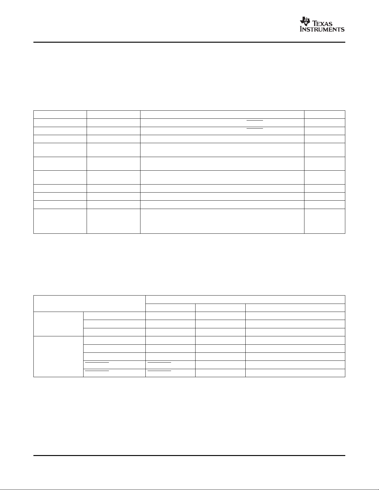
www.ti.com
TMS320C6727, TMS320C6726, TMS320C6722
Floating-Point Digital Signal Processors
SPRS268E – MAY 2005 – REVISED JANUARY 2007
3 Device Configurations
3.1 Device Configuration Registers
The C672x DSP includes several device-level configuration registers, which are listed in Table 3-1 . These
registers need to be programmed as part of the device initialization procedure. See Section 3.2 .
Table 3-1. Device-Level Configuration Registers
REGISTER NAME BYTE ADDRESS DESCRIPTION DEFINED
CFGPIN0 0x4000 0000 Captures values of eight pins on rising edge of RESET pin. Table 2-10
CFGPIN1 0x4000 0004 Captures values of eight pins on rising edge of RESET pin. Table 2-11
CFGHPI 0x4000 0008 Controls enable of UHPI and selection of its operating mode. Table 4-12
CFGHPIAMSB 0x4000 000C Controls upper byte of UHPI address into C672x address space in Table 4-13
CFGHPIAUMB 0x4000 0010 Controls upper middle byte of UHPI address into C672x address space Table 4-14
CFGRTI 0x4000 0014 Selects the sources for the RTI Input Captures from among the six Table 4-37
CFGMCASP0 0x4000 0018 Selects the peripheral pin to be used as AMUTEIN0. Table 4-19
CFGMCASP1 0x4000 001C Selects the peripheral pin to be used as AMUTEIN1. Table 4-20
CFGMCASP2
CFGBRIDGE 0x4000 0024 Controls reset of the bridge BR2 in Figure 2-4 . This bridge must be reset Table 2-7
(1) CFGMCASP2 is reserved on the C6722.
(1)
0x4000 0020 Selects the peripheral pin to be used as AMUTEIN2. Table 4-21
Non-Multiplexed Mode or if explicitly enabled for security purposes.
in Non-Multiplexed Mode or if explicitly enabled for security purposes.
McASP DMA events.
explicitly after any change to the PLL controller affecting SYSCLK1 and
SYSCLK2 and before the dMAX or UHPI accesses the CPU Slave Port
(CSP).
3.2 Peripheral Pin Multiplexing Options
This section describes the options for configuring peripherals which share pins on the C672x DSP.
Table 3-2 lists the options for configuring the SPI0, I2C0, and I2C1 peripheral pins.
Table 3-2. Options for Configuring SPI0, I2C0, and I2C1
OPTION 1 OPTION 2 OPTION 3
PERIPHERAL SPI0 3-, 4,- or 5-pin mode 3-pin mode disabled
I2C0 disabled disabled enabled
I2C1 disabled enabled enabled
PINS SPI0_SOMI/I2C0_SDA SPI0_SOMI SPI0_SOMI I2C0_SDA
SPI0_SIMO SPI0_SIMO SPI0_SIMO GPIO through SPI0_SIMO pin control
SPI0_CLK/I2C0_SCL SPI0_CLK SPI0_CLK I2C0_SCL
SPI0_SCS/I2C1_SCL SPI0_SCS I2C1_SCL I2C1_SCL
SPI0_ENA/I2C1_SDA SPI0_ENA I2C1_SDA I2C1_SDA
CONFIGURATION
Device Configurations30 Submit Documentation Feedback
Page 31

www.ti.com
TMS320C6727, TMS320C6726, TMS320C6722
Floating-Point Digital Signal Processors
SPRS268E – MAY 2005 – REVISED JANUARY 2007
Table 3-3 lists the options for configuring the SPI1, McASP0, and McASP1 pins. Note that there are
additional finer grain options when selecting which McASP controls the particular AXR serial data pins but
these options are not listed here and can be made on a pin by pin basis.
Table 3-3. Options for Configuring SPI1, McASP0, and McASP1 Data Pins
CONFIGURATION
OPTION 1 OPTION 2 OPTION 3 OPTION 4 OPTION 5
PERIPHERAL SPI1 5-pin mode 4-pin mode 4-pin mode 3-pin mode disabled
McASP0 11 12 12 13 16
(max data pins)
McASP1 4 4 4 4 6
(max data pins)
PINS AXR0[5]/ SPI1_SCS SPI1_SCS AXR0[5] AXR0[5] AXR0[5]
SPI1_SCS
AXR0[6]/ SPI1_ENA AXR0[6] SPI1_ENA AXR0[6] AXR0[6]
SPI1_ENA
AXR0[7]/ SPI1_CLK SPI1_CLK SPI1_CLK SPI1_CLK AXR0[7]
SPI1_CLK
AXR0[8]/AXR1[5]/ SPI1_SOMI SPI1_SOMI SPI1_SOMI SPI1_SOMI AXR0[8] or AXR1[5]
SPI1_SOMI
AXR0[9]/AXR1[4]/ SPI1_SIMO SPI1_SIMO SPI1_SIMO SPI1_SIMO AXR0[9] or AXR1[4]
SPI1_SIMO
Table 3-4 lists the options for configuring the shared EMIF and UHPI pins.
Table 3-4. Options for Configuring EMIF and UHPI (C6727 Only)
CONFIGURATION
OPTION 1 OPTION 2
PERIPHERAL UHPI Multiplexed Address/Data Mode, Fullword, or Non-Multiplexed Address/Data Mode
EMIF 32-bit EMIF Data 16-bit EMIF Data
PINS EM_D[31:16]/ EM_D[31:16] UHPI_HA[15:0]
UHPI_HA[15:0]
Half-Word Fullword
3.3 Peripheral Pin Multiplexing Control
While Section 3.2 describes at a high level the most common pin multiplexing options, the control of pin
multiplexing is largely determined on an individual pin-by-pin basis. Typically, each peripheral that shares
a particular pin has internal control registers to determine the pin function and whether it is an input or an
output.
The C672x device determines whether a particular pin is an input or output based upon the following
rules:
• The pin will be configured as an output if it is configured as an output in any of the peripherals sharing
the pin.
• It is recommended that only one peripheral configure a given pin as an output. If more than one
peripheral does configure a particular pin as an output, then the output value is controlled by the
peripheral with highest priority for that pin. The priorities for each pin are given in Table 3-5 .
• The value input on the pin is passed to all peripherals sharing the pin for input simultaneously.
Submit Documentation Feedback Device Configurations 31
Page 32

www.ti.com
TMS320C6727, TMS320C6726, TMS320C6722
Floating-Point Digital Signal Processors
SPRS268E – MAY 2005 – REVISED JANUARY 2007
Table 3-5. Priority of Control of Data Output on Multiplexed Pins
PIN FIRST PRIORITY SECOND PRIORITY THIRD PRIORITY
SPI0_SOMI/I2C0_SDA SPI0_SOMI I2C0_SDA
SPI0_CLK/I2C0_SCL SPI0_CLK I2C0_SCL
SPI0_SCS/I2C1_SCL SPI0_SCS I2C1_SCL
SPI0_ENA/I2C1_SDA SPI0_ENA I2C1_SDA
AXR0[5]/ SPI1_SCS AXR0[5] SPI1_SCS
AXR0[6]/ SPI1_ENA AXR0[6] SPI1_ENA
AXR0[7]/SPI1_CLK AXR0[7] SPI1_CLK
AXR0[8]/AXR1[5]/SPI1_SOMI AXR0[8] AXR1[5] SPI1_SOMI
AXR0[9]/AXR1[4]/SPI1_SIMO AXR0[9] AXR1[4] SPI1_SIMO
AXR0[10]/AXR1[3] AXR0[10] AXR1[3]
AXR0[11]/AXR1[2] AXR0[11] AXR1[2]
AXR0[12]/AXR1[1] AXR0[12] AXR1[1]
AXR0[13]/AXR1[0] AXR0[13] AXR1[0]
AXR0[14]/AXR2[1] AXR0[14] AXR2[1]
AXR0[15]/AXR2[0] AXR0[15] AXR2[0]
AHCLKR0/AHCLKR1 AHCLKR0 AHCLKR1
AHCLKX0/AHCLKX2 AHCLKX0 AHCLKX2
AMUTE2/HINT AMUTE2 HINT
HD[16]/HHWIL HD[16] HHWIL
EM_D[31:16]/UHPI_HA[15:0]
(1)
EM_D[31:16] (Disabled if UHPI_HA[15:0] (Input Only)
CFGHPI.NMUX=1)
(1) When using the UHPI in non-multiplexed mode, ensure EM_D[31:16] are configured as inputs so that these pins may be used as
UHPI_HA[15:0]. To ensure this, you must set the CFGHPI.NMUX bit to a '1' before the EMIF SDRAM initialization completes;
otherwise, a drive conflict will occur. [The EMIF bus parking function drives the data bus in between accesses.]
32 Device Configurations Submit Documentation Feedback
Page 33

www.ti.com
4 Peripheral and Electrical Specifications
4.1 Electrical Specifications
This section provides the absolute maximum ratings and the recommended operating conditions for the
TMS320C672x DSP.
All electrical and switching characteristics in this data manual are valid over the recommended operating
conditions unless otherwise specified.
TMS320C6727, TMS320C6726, TMS320C6722
Floating-Point Digital Signal Processors
SPRS268E – MAY 2005 – REVISED JANUARY 2007
4.2 Absolute Maximum Ratings
(1) (2)
Over Operating Case Temperature Range (Unless Otherwise Noted)
Supply voltage range, CV
Supply voltage range, DV
, OSCV
DD
, PLLHV –0.3 to 4 V
DD
Input Voltage Range All pins except OSCIN –0.3 to DV
Output Voltage Range All pins except OSCOUT –0.3 to DV
Clamp Current ± 20 mA
Operating case temperature range T
Storage temperature range, T
stg
(1) Stresses beyond those listed under "absolute maximum ratings" may cause permanent damage to the device. These are stress ratings
only, and functional operation of the device at these or any conditions beyond those indicated under "recommended operating
conditions" is not implied. Exposure to absolute-maximum-rated conditions for extended periods may affect device reliability.
(2) All voltage values are with referenced to V
(3) If OSCV
externally.
and OSCV
DD
pins are used as filter pins for reduced oscillator jitter, they should not be connected to CV
SS
4.3 Recommended Operating Conditions
CV
DD
DV
DD
T
C
(1) All voltage values are with referenced to V
Core Supply Voltage 1.14 1.2 1.32 V
I/O Supply Voltage 3.13 3.3 3.47 V
Operating Case Temperature Range Default 0 90
(3)
DD
OSCIN pin –0.3 to CV
OSCOUT pin –0.3 to CV
C
Default 0 to 90
–0.3 to 1.8 V
+ 0.5
DD
+ 0.5
DD
+ 0.5
DD
+ 0.5
DD
A version –40 to 105
–65 to 150 ° C
unless otherwise specified.
SS
(1)
and V
DD
MIN NOM MAX UNIT
A version –40 105
unless otherwise specified.
SS
UNIT
V
V
° C
SS
° C
Submit Documentation Feedback Peripheral and Electrical Specifications 33
Page 34

www.ti.com
TMS320C6727, TMS320C6726, TMS320C6722
Floating-Point Digital Signal Processors
SPRS268E – MAY 2005 – REVISED JANUARY 2007
4.4 Electrical Characteristics
Over Operating Case Temperature Range (Unless Otherwise Noted)
PARAMETER TEST CONDITIONS MIN TYP MAX UNIT
V
OH
V
OL
I
OH
I
OL
V
IH
V
IL
V
HYS
II, I
OZ
t
tr
C
I
C
O
I
DD2V
I
DD3V
(1) Assumes the following conditions: 25 ° C case temperature; 60% CPU utilization; EMIF at 50% utilization (100 MHz), 50% writes, (32 bits
for GDH, 16 bits for RFP), 50% bit switching; two 10-MHz SPI at 100% utilization, 50% bit switching.
The actual current draw is highly application-dependent. For more details on core and I/O activity, refer to the TMS320C672x Power
Consumption Summary Application Report (literature number SPRAAA4 ).
High Level Output Voltage IO= –100 µA DV
– 0.2 V
DD
Low Level Output Voltage IO= 100 µA 0.2 V
High-Level Output Current VO= 0.8 DV
Low-Level Output Current VO= 0.22 DV
DD
DD
High-Level Input Voltage 2 DV
–8 mA
8 mA
DD
Low-Level Input Voltage 0 0.8 V
Input Hysterisis 0.13 DV
DD
Input Current and Off State Output Pins without pullup or pulldown ± 10
Current
Pins with internal pullup –50 –170 µA
Pins with internal pulldown 50 170
Input Transition Time 25 ns
Input Capacitance 7 pF
Output Capacitance 7 pF
CV
DD
DV
DD
(1)
Supply
(1)
Supply
GDH, CV
CPU clock = 300 MHz
RFP, CV
CPU clock = 250 MHz
GDH, DV
32-bit EMIF speed = 100 MHz
RFP, DV
16-bit EMIF speed = 100 MHz
= 1.2 V, 658
DD
= 1.2 V, 555
DD
= 3.3 V, 76
DD
= 3.3 V, 58
DD
V
V
mA
mA
34 Peripheral and Electrical Specifications Submit Documentation Feedback
Page 35

www.ti.com
Transmission Line
4.0 pF 1.85 pF
Z0 = 50 Ω
(see note)
Tester Pin Electronics
Data Sheet Timing Reference Point
Output
Under
Test
42 Ω 3.5 nH
Device Pin
(see note)
V
ref
= 1.5 V
V
ref
= VIL MAX (or VOL MAX)
V
ref
= VIH MIN (or VOH MIN)
TMS320C6727, TMS320C6726, TMS320C6722
Floating-Point Digital Signal Processors
SPRS268E – MAY 2005 – REVISED JANUARY 2007
4.5 Parameter Information
4.5.1 Parameter Information Device-Specific Information
A. The data sheet provides timing at the device pin. For output timing analysis, the tester pin electronics and its
transmission line effects must be taken into account. A transmission line with a delay of 2 ns or longer can be used to
produce the desired transmission line effect. The transmission line is intended as a load only. It is not neccessary to
add or subtract the transmission line delay (2 ns or longer) from the data sheet timings.
Input requirements in this data sheet are tested with an input slew rate of < 4 Volts per nanosecond (4 V/ns) at the
device pin.
4.5.1.1 Signal Transition Levels
All input and output timing parameters are referenced to 1.5 V for both "0" and "1" logic levels.
Figure 4-2. Input and Output Voltage Reference Levels for AC Timing Measurements
All rise and fall transition timing parameters are referenced to V
V
MAX and V
OL
4.5.1.2 Signal Transition Rates
All timings are tested with an input edge rate of 4 Volts per nanosecond (4 V/ns).
Figure 4-1. Test Load Circuit for AC Timing Measurements
MAX and V
MIN for output clocks.
OH
IL
Figure 4-3. Rise and Fall Transition Time Voltage Reference Levels
MIN for input clocks,
IH
Submit Documentation Feedback Peripheral and Electrical Specifications 35
Page 36

www.ti.com
TMS320C6727, TMS320C6726, TMS320C6722
Floating-Point Digital Signal Processors
SPRS268E – MAY 2005 – REVISED JANUARY 2007
4.6 Timing Parameter Symbology
Timing parameter symbols used in the timing requirements and switching characteristics tables are
created in accordance with JEDEC Standard 100. To shorten the symbols, some of the pin names and
other related terminology have been abbreviated as follows:
Lowercase subscripts and their meanings: Letters and symbols and their meanings:
a access time H High
c cycle time (period) L Low
d delay time V Valid
dis disable time Z High impedance
en enable time
f fall time
h hold time
r rise time
su setup time
t transition time
v valid time
w pulse duration (width)
X Unknown, changing, or don't care level
Peripheral and Electrical Specifications36 Submit Documentation Feedback
Page 37

www.ti.com
4.7 Power Supplies
For more information regarding TI’s power management products and suggested devices to power TI
DSPs, visit www.ti.com/dsppower .
4.7.1 Power-Supply Sequencing
TMS320C6727, TMS320C6726, TMS320C6722
Floating-Point Digital Signal Processors
SPRS268E – MAY 2005 – REVISED JANUARY 2007
This device does not require specific power-up sequencing between the DV
however, there are some considerations that the system designer should take into account:
1. Neither supply should be powered up for an extended period of time (>1 second) while the other
2. The I/O buffers powered from the DV
4.7.2 Power-Supply Decoupling
In order to properly decouple the supply planes from system noise, place as many capacitors (caps) as
possible close to the DSP. The core supply caps can be placed in the interior space of the package and
the I/O supply caps can be placed around the exterior space of the package. For the BGA package, it is
recommended that both the core and I/O supply caps be placed on the underside of the PCB. For the
TQFP package, it is recommended that the core supply caps be placed on the underside of the PCB and
the I/O supply caps be placed on the top side of the PCB.
Both core and I/O decoupling can be accomplished by alternating small (0.1 µ F) low ESR ceramic bypass
caps with medium (0.220 µ F) low ESR ceramic bypass caps close to the DSP power pins and adding
large tantalum or ceramic caps (ranging from 10 µ F to 100 µ F) further away. Assuming 0603 caps, it is
recommended that at least 6 small, 6 medium, and 4 large caps be used for the core supply and 12 small,
12 medium, and 4 large caps be used for the I/O supply.
and CV
DD
supply is powered down.
rail also require the CV
DD
rail to be powered up in order to be
DD
controlled; therefore, an I/O pin that is supposed to be 3-stated by default may actually drive
momentarily until the CV
rail has powered up. Systems should be evaluated to determine if there is
DD
a possibility for contention that needs to be addressed. In most systems where both the DV
CV
supplies ramp together, as long as CV
DD
the fact that the CV
rail would reach its specified operating range well before the DV
DD
tracks DV
DD
closely, any contention is also mitigated by
DD
ramped.
voltage rails;
DD
and
DD
rail has fully
DD
Any cap selection needs to be evaluated from an electromagnetic radiation (EMI) point-of-view; EMI varies
from one system design to another so it is expected that engineers alter the decoupling capacitors to
minimize radiation. Refer to the High-Speed DSP Systems Design Reference Guide (literature number
SPRU889) for more detailed design information on decoupling techniques.
Submit Documentation Feedback Peripheral and Electrical Specifications 37
Page 38

www.ti.com
TMS320C6727, TMS320C6726, TMS320C6722
Floating-Point Digital Signal Processors
SPRS268E – MAY 2005 – REVISED JANUARY 2007
4.8 Reset
A hardware reset ( RESET) is required to place the DSP into a known good state out of power-up. The
RESET signal can be asserted (pulled low) prior to ramping the core and I/O voltages or after the core
and I/O voltages have reached their proper operating conditions. As a best practice, RESET should be
held low during power-up. Prior to deasserting RESET (low-to-high transition), the core and I/O voltages
should be at their proper operating conditions.
4.8.1 Reset Electrical Data/Timing
Table 4-1 assumes testing over recommended operating conditions.
Table 4-1. Reset Timing Requirements
NO. MIN MAX UNIT
1 t
2 t
3 t
w(RSTL)
su(BPV-RSTH)
h(RSTH-BPV)
Pulse width, RESET low 100 ns
Setup time, boot pins valid before RESET high 20 ns
Hold time, boot pins valid after RESET high 20 ns
Peripheral and Electrical Specifications38 Submit Documentation Feedback
Page 39

www.ti.com
4.9 Dual Data Movement Accelerator (dMAX)
4.9.1 dMAX Device-Specific Information
The dMAX is a module designed to perform Data Movement Acceleration. The dMAX controller handles
user-programmed data transfers between the internal data memory controller and the device peripherals
on the C672x DSP. The dMAX allows movement of data to/from any addressable memory space,
including internal memory, peripherals, and external memory. The dMAX controller in the C672x DSP has
a different architecture from the previous EDMA controller in the C621x/C671x devices.
The dMAX controller includes features, such as capability to perform three-dimensional data transfers for
advanced data sorting, capability to manage a section of the memory as a circular buffer/FIFO with delay
tap based reading and writing data. The dMAX controller is capable of concurrently processing two
transfer requests (provided that they are to/from different source/destinations).
Figure 4-4 shows a block diagram of the dMAX controller.
TMS320C6727, TMS320C6726, TMS320C6722
Floating-Point Digital Signal Processors
SPRS268E – MAY 2005 – REVISED JANUARY 2007
Submit Documentation Feedback Peripheral and Electrical Specifications 39
Page 40

www.ti.com
Event Entry #0
Event Entry #k
Event Entry #31
Transfer Entry #0
Transfer Entry #k
Transfer Entry #7
Reserved
Event
Entry
Table
Transfer
Entry
Table
HiMAX
RAM
R/W
Control
R/W
HiMAX
(MAX0)
Event
Encoder
+
Event and
Interrupt
Registers
LoMAX
(MAX1)
Transfer
Entry
Table
LoMAX
RAM
R/W
Transfer Entry #7
Transfer Entry #k
Transfer Entry #0
Event Entry #31
Reserved
Event
Table
Entry
Event Entry #k
Event Entry #0
High-Priority
REQ
Low-Priority
REQ
High-Priority PaRAM
To/From
Crossbar
Switch
LoMAX
Master
Crossbar
Switch
Port
Events
Interrupt
Lines to
the CPU
HiMAX
Master
Crossbar
Switch
Port
dMAX
Low-Priority PaRAM
TMS320C6727, TMS320C6726, TMS320C6722
Floating-Point Digital Signal Processors
SPRS268E – MAY 2005 – REVISED JANUARY 2007
Peripheral and Electrical Specifications40 Submit Documentation Feedback
Figure 4-4. dMAX Controller Block Diagram
Page 41

www.ti.com
TMS320C6727, TMS320C6726, TMS320C6722
Floating-Point Digital Signal Processors
SPRS268E – MAY 2005 – REVISED JANUARY 2007
The dMAX controller comprises:
• Event and interrupt processing registers
• Event encoder
• High-priority event Parameter RAM (PaRAM)
• Low-priority event Parameter RAM (PaRAM)
• Address-generation hardware for High-Priority Events – MAX0 (HiMAX)
• Address-generation hardware for Low-Priority Events – MAX1 (LoMAX)
The TMS320C672x Peripheral Bus Structure can be described logically as a Crossbar Switch with five
master ports and five slave ports. When accessing the slave ports, the MAX0 (HiMAX) module is always
given the highest priority followed by the MAX1 (LoMAX) module. In other words, in case several masters
(including MAX0 and MAX1) attempt to access same slave port concurrently, the MAX0 will be given the
highest priority followed by MAX1.
Event signals are connected to bits of the dMAX Event Register (DER), and the bits in the DER reflect the
current state of the event signals. An event is defined as a transition of the event signal. The dMAX Event
Flag Register (DEFR) can be programmed, individually for each event signal, to capture either low-to-high
or high-to-low transitions of the bits in the DER (event polarity is individually programmable).
An event is a synchronization signal that can be used: 1) to either trigger dMAX to start a transfer, or 2) to
generate an interrupt to the CPU. All the events are sorted into two groups: low-priority event group and
high-priority event group.
The High-Priority Data Movement Accelerator MAX0 (HiMAX) module is dedicated to serving requests
coming from the high-priority event group. The Low-Priority Data Movement Accelerator MAX1 (LoMAX)
module is dedicated to serving requests coming from the low-priority event group.
Each PaRAM contains two sections: the event entry table section and the transfer entry table section. An
event entry describes an event type and associates the event to either one of transfer types or to an
interrupt. In case an event entry associates the event to one of the transfer types, the event entry will
contain a pointer to the specific transfer entry in the transfer entry table. The transfer table may contain up
to eight transfer entries. A transfer entry specifies details required by the dMAX controller to perform the
transfer. In case an event entry associates the event to an interrupt, the event entry specifies which
interrupt should be generated to the CPU in case the event arrives.
Prior to enabling events and triggering a transfer, the event entry and transfer entry must be configured.
The event entry must specify: type of transfer, transfer details (type of synchronization, reload, element
size, etc.), and should include a pointer to the transfer entry. The transfer entry must specify: source,
destination, counts, and indexes. If an event is sorted in the high-priority event group, the event entry and
transfer entry must be specified in the high-priority Parameter RAM. If an event is sorted in the low-priority
event group, the event entry and transfer entry must be specified in the low-priority parameter RAM.
The dMAX Event Flag Register (DEFR) captures up to 31 separate events; therefore, it is possible for
events to occur simultaneously on the dMAX event inputs. In such cases, the event encoder resolves the
order of processing. This mechanism sorts simultaneous events and sets the priority of the events. The
dMAX controller can simultaneously process one event from each priority group. Therefore, the two
highest-priority events (one from each group) can be processed at the same time.
An event-triggered dMAX transfer allows the submission of transfer requests to occur automatically based
on system events, without any intervention by the CPU. The dMAX also includes support for CPU-initiated
transfers for added control and robustness, and they can be used to start memory-to-memory transfers.
To generate an event to the dMAX controller the CPU must create a transition on one of the bits from the
dMAX Event Trigger (DETR) Register, which are mapped to the DER register.
Submit Documentation Feedback Peripheral and Electrical Specifications 41
Page 42

www.ti.com
TMS320C6727, TMS320C6726, TMS320C6722
Floating-Point Digital Signal Processors
SPRS268E – MAY 2005 – REVISED JANUARY 2007
Table 4-2 lists how the synchronization events are associated with event numbers in the dMAX controller.
Table 4-2. dMAX Peripheral Event Input Assignments
EVENT NUMBER EVENT ACRONYM EVENT DESCRIPTION
0 DETR[0] The CPU triggers the event by creating appropriate transition (edge) on bit0
1 DETR[16] The CPU triggers the event by creating appropriate transition (edge) on bit16
2 RTIREQ0 RTI DMA REQ[0]
3 RTIREQ1 RTI DMA REQ[1]
4 MCASP0TX McASP0 TX DMA REQ
5 MCASP0RX McASP0 RX DMA REQ
6 MCASP1TX McASP1 TX DMA REQ
7 MCASP1RX McASP1 RX DMA REQ
8 MCASP2TX McASP2 TX DMA REQ
9 MCASP2RX McASP2 RX DMA REQ
10 DETR[1] The CPU triggers the event by creating appropriate transition (edge) on bit1
11 DETR[17] The CPU triggers the event by creating appropriate transition (edge) on bit17
12 UHPIINT UHPI CPU_INT
13 SPI0RX SPI0 DMA_RX_REQ
14 SPI1RX SPI1 DMA_RX_REQ
15 RTIREQ2 RTI DMA REQ[2]
16 RTIREQ3 RTI DMA REQ[3]
17 DETR[2] The CPU triggers the event by creating appropriate transition (edge) on bit2
18 DETR[18] The CPU triggers the event by creating appropriate transition (edge) on bit18
19 I2C0XEVT I2C 0 Transmit Event
20 I2C0REVT I2C 0 Receive Event
21 I2C1XEVT I2C 1 Transmit Event
22 I2C1REVT I2C 1 Receive Event
23 DETR[3] The CPU triggers the event by creating appropriate transition (edge) on bit3
24 DETR[19] The CPU triggers the event by creating appropriate transition (edge) on bit19
25 Reserved
26 MCASP0ERR AMUTEIN0 or McASP0 TX INT or McASP0 RX INT (error on McASP0)
27 MCASP1ERR AMUTEIN1 or McASP1 TX INT or McASP1 RX INT (error on McASP1)
28 MCASP2ERR AMUTEIN2 or McASP2 TX INT or McASP2 RX INT (error on McASP2)
29 OVLREQ[0/1] Error on RTI
30 DETR[20] The CPU triggers the event by creating appropriate transition (edge) on bit20
31 DETR[21] The CPU triggers the event by creating appropriate transition (edge) on bit21
in DETR register.
in DETR register.
in DETR register.
in DETR register.
in DETR register.
in DETR register.
in DETR register.
in DETR register.
in DETR register.
in DETR register.
Peripheral and Electrical Specifications42 Submit Documentation Feedback
Page 43

www.ti.com
4.9.2 dMAX Peripheral Registers Description(s)
Table 4-3 is a list of the dMAX registers.
Table 4-3. dMAX Configuration Registers
BYTE ADDRESS REGISTER NAME DESCRIPTION
0x6000 0008 DEPR Event Polarity Register
0x6000 000C DEER Event Enable Register
0x6000 0010 DEDR Event Disable Register
0x6000 0014 DEHPR Event High-priority Register
0x6000 0018 DELPR Event Low-priority Register
0x6000 001C DEFR Event Flag Register
0x6000 0034 DER0 Event Register 0
0x6000 0054 DER1 Event Register 1
0x6000 0074 DER2 Event Register 2
0x6000 0094 DER3 Event Register 3
0x6000 0040 DFSR0 FIFO Status Register 0
0x6000 0060 DFSR1 FIFO Status Register 1
0x6000 0080 DTCR0 Transfer Complete Register 0
0x6000 00A0 DTCR1 Transfer Complete Register 1
N/A DETR Event Trigger Register (Located in C67x+ DSP Register File)
N/A DESR Event Status Register (Located in C67x+ DSP Register File)
TMS320C6727, TMS320C6726, TMS320C6722
Floating-Point Digital Signal Processors
SPRS268E – MAY 2005 – REVISED JANUARY 2007
Submit Documentation Feedback Peripheral and Electrical Specifications 43
Page 44

www.ti.com
TMS320C6727, TMS320C6726, TMS320C6722
Floating-Point Digital Signal Processors
SPRS268E – MAY 2005 – REVISED JANUARY 2007
4.10 External Interrupts
The C672x DSP has no dedicated general-purpose interrupt pins, but the dMAX can be used in
combination with a McASP AMUTEIN signal to provide external interrupt capability. There is a multiplexer
for each McASP, controlled by the CFGMCASP0/1/2 registers, which allows the AMUTEIN input for that
McASP to be sourced from one of seven I/O pins on the DSP. Once a pin is configured as an AMUTEIN
source, a very short pulse (two SYSCLK2 cycles or more) on that pin will generate an event to the dMAX.
This event can trigger the dMAX to generate a CPU interrupt by programming the assoicated Event Entry.
There are a few additional points to consider when using the AMUTEIN signal to enable external interrupts
as described above. The I/O pin selected by the CFGMCASP0/1/2 registers must be configured as a
general-purpose input pin within the associated peripheral. Also, the AMUTEIN signal should be disabled
within the corresponding McASP so that AMUTE is not driven when AMUTEIN is active. This can be done
by clearing the INEN bit of the AMUTE register inside the McASP. Finally, AMUTEIN events are logically
ORed with the McASP transmit and receive error events within the dMAX; therefore, the ISR that
processes the dMAX interrupt generated by these events must discern the source of the event.
The EMIF EM_WAIT pin has the ability to generate an NMI (INT1) based upon a rising edge on the
EM_WAIT pin. Note that while this interrupt is connected to the CPU NMI (non-maskable interrupt), it is
actually maskable through the EMIF control registers. In fact, the default state for this interrupt is disabled.
Also, interrupt generation always occurs on a rising edge of EM_WAIT; the polarity selection for wait state
generation has no effect on the interrupt polarity. The EM_WAIT pin should remain asserted for at least
two SYSCLK3 cycles to ensure that the edge is detected.
Peripheral and Electrical Specifications44 Submit Documentation Feedback
Page 45

www.ti.com
4.11 External Memory Interface (EMIF)
4.11.1 EMIF Device-Specific Information
The C672x DSP includes an external memory interface (EMIF) for optional SDRAM, NOR FLASH, NAND
FLASH, or SRAM. The key features of this EMIF are:
• One chip select ( EM_CS[0]) dedicated for x16 and x32 SDRAM (x8 not supported)
• One chip select ( EM_CS[2]) dedicated for x8, x16, or x32 NOR FLASH; x8, x16, or x32 Asynchronous
SRAM; or x8 or x16 NAND FLASH
• Data bus width is 16 bits on the C6726 and C6722, and 32 bits on the C6727
• SDRAM burst length of 16 bytes
• External Wait Input on the C6727 through EM_WAIT (programmable active-high or active-low)
• External Wait pin functions as an interrupt for NAND Flash support
• NAND Flash logic calculates ECC on blocks of up to 512 bytes
• ECC logic suitable for single-bit errors
Figure 4-5 and Figure 4-6 show typical examples of EMIF-to-memory hookup on the C672x DSP.
As the figures illustrate, the C672x DSP includes a limited number of EMIF address lines. These are
sufficient to connect to SDRAM seamlessly. Asynchronous memory such as FLASH typically will need to
use additional GPIO pins to act as upper address lines during device boot up when the FLASH contents
are copied into SDRAM. (Normally, code is executed from SDRAM since SDRAM has faster access
times).
TMS320C6727, TMS320C6726, TMS320C6722
Floating-Point Digital Signal Processors
SPRS268E – MAY 2005 – REVISED JANUARY 2007
Any pins listed with a ‘Y' in the GPIO column of Table 2-12 may be used for this purpose, as long as it can
be assured that they be pulled low at (and after) reset and held low until configured as outputs by the
DSP.
Note that EM_BA[1:0] are used as low-order address lines for the asynchronous interface. For example, in
Figure 4-5 and Figure 4-6 , the flash memory is not byte-addressable and its A[0] input selects a 16-bit
value. The corresponding DSP address comes from EM_BA[1]. The remaining address lines from the
DSP (EM_A[12:0]) drive a word address into the flash inputs A[13:1].
For a more detailed explanation of the C672x EMIF operation please refer to the document
TMS320C672x External Memory Interface (EMIF) User's Guide (literature number SPRU711).
Submit Documentation Feedback Peripheral and Electrical Specifications 45
Page 46

www.ti.com
EM_CS[0]
EM_CAS
EM_RAS
EM_WE
EM_CLK
EM_CKE
EM_BA[1:0]
EM_A[11:0]
EM_WE_DQM[0]
EM_WE_DQM[1]
EM_D[15:0]
EM_CS[2]
EM_RW
EM_OE
GPIO
(6 Pins)RESET
C6726/C6722
DSP EMIF
CE
CAS
RAS
WE
CLK
CKE
BA[1:0]
A[11:0]
LDQM
UDQM
DQ[15:0]
2M x 16 x 4 Bank
SDRAM
A[18:13]
RY/BY
RESET
OE
WE
CE
DQ[15:0]
512K x 16
A[0]
A[12:1]
FLASH
EM_BA[1]
RESET
Any GPIO-capable pins which
can be pulled down at reset
can be used to control A[18:13]
for FLASH BOOTLOAD
Examples: AHCLKR0, SPI0_SCS
/SCL1
TMS320C6727, TMS320C6726, TMS320C6722
Floating-Point Digital Signal Processors
SPRS268E – MAY 2005 – REVISED JANUARY 2007
Peripheral and Electrical Specifications46 Submit Documentation Feedback
Figure 4-5. C6726/C6722 DSP 16-Bit EMIF Example
Page 47

www.ti.com
EM_CS[0]
EM_CAS
EM_RAS
EM_WE
EM_CLK
EM_CKE
EM_BA[1:0]
EM_A[12:0]
EM_WE_DQM[0]
EM_WE_DQM[1]
EM_D[15:0]
EM_WE_DQM[2]
GPIO
(5 Pins)
RESET
C6727
DSP EMIF
CE
CAS
RAS
WE
CLK
CKE
BA[1:0]
A[12:0]
LDQM
UDQM
DQ[15:0]
4M x 16 x 4 Bank
SDRAM
A[18:14]
RY/BY
RESET
OE
WE
CE
DQ[15:0]
512K x 16
A[0]
A[13:1]
FLASH
EM_BA[1]
RESET
Any GPIO-capable pins which
can be pulled down at reset
can be used to control A[18:14]
for FLASH BOOTLOAD
Examples: AHCLKR0, SPI0_SCS
/SCL1
EM_WE
_DQM[3]
EM_D[31:16]/UHPI_HA[15:0]
EM_CS[2]
EM_RW
EM_OE
EM_WAIT
BA[1:0]
A[12:0]
DQ[15:0]
LDQM
UDQM
4M x 16 x 4 Bank
RAS
CLK
CKE
WE
CAS
CE
SDRAM
TMS320C6727, TMS320C6726, TMS320C6722
Floating-Point Digital Signal Processors
SPRS268E – MAY 2005 – REVISED JANUARY 2007
Figure 4-6. C6727 DSP 32-Bit EMIF Example
Submit Documentation Feedback Peripheral and Electrical Specifications 47
Page 48

www.ti.com
TMS320C6727, TMS320C6726, TMS320C6722
Floating-Point Digital Signal Processors
SPRS268E – MAY 2005 – REVISED JANUARY 2007
4.11.2 EMIF Peripheral Registers Description(s)
Table 4-4 is a list of the EMIF registers. For more information about these registers, see the
TMS320C672x DSP External Memory Interface (EMIF) User's Guide (literature number SPRU711).
Table 4-4. EMIF Registers
BYTE ADDRESS REGISTER NAME DESCRIPTION
0xF000 0004 AWCCR Asynchronous Wait Cycle Configuration Register
0xF000 0008 SDCR SDRAM Configuration Register
0xF000 000C SDRCR SDRAM Refresh Control Register
0xF000 0010 A1CR Asynchronous 1 Configuration Register
0xF000 0020 SDTIMR SDRAM Timing Register
0xF000 003C SDSRETR SDRAM Self Refresh Exit Timing Register
0xF000 0040 EIRR EMIF Interrupt Raw Register
0xF000 0044 EIMR EMIF Interrupt Mask Register
0xF000 0048 EIMSR EMIF Interrupt Mask Set Register
0xF000 004C EIMCR EMIF Interrupt Mask Clear Register
0xF000 0060 NANDFCR NAND Flash Control Register
0xF000 0064 NANDFSR NAND Flash Status Register
0xF000 0070 NANDF1ECC NAND Flash 1 ECC Register
Peripheral and Electrical Specifications48 Submit Documentation Feedback
Page 49

www.ti.com
TMS320C6727, TMS320C6726, TMS320C6722
Floating-Point Digital Signal Processors
SPRS268E – MAY 2005 – REVISED JANUARY 2007
4.11.3 EMIF Electrical Data/Timing
Table 4-5 through Table 4-8 assume testing over recommended operating conditions (see Figure 4-7
through Figure 4-13 ).
Table 4-5. EMIF SDRAM Interface Timing Requirements
NO. MIN MAX UNIT
19 t
su(EM_DV-EM_CLKH)
20 t
h(EM_CLKH-EM_DIV)
Table 4-6. EMIF SDRAM Interface Switching Characteristics
NO. PARAMETER MIN MAX UNIT
1 t
c(EM_CLK)
2 t
w(EM_CLK)
3 t
d(EM_CLKH-EM_CSV)S
4 t
oh(EM_CLKH-EM_CSIV)S
5 t
d(EM_CLKH-EM_WE-DQMV)S
6 t
oh(EM_CLKH-EM_WE-DQMIV)S
7 t
d(EM_CLKH-EM_AV)S
8 t
oh(EM_CLKH-EM_AIV)S
9 t
d(EM_CLKH-EM_DV)S
10 t
oh(EM_CLKH-EM_DIV)S
11 t
d(EM_CLKH-EM_RASV)S
12 t
oh(EM_CLKH-EM_RASIV)S
13 t
d(EM_CLKH-EM_CASV)S
14 t
oh(EM_CLKH-EM_CASIV)S
15 t
d(EM_CLKH-EM_WEV)S
16 t
oh(EM_CLKH-EM_WEIV)S
17 t
dis(EM_CLKH-EM_DHZ)S
18 t
ena(EM_CLKH-EM_DLZ)S
Input setup time, read data valid on D[31:0] before EM_CLK rising 3 ns
Input hold time, read data valid on D[31:0] after EM_CLK rising 1.9 ns
Cycle time, EMIF clock EM_CLK 10 ns
Pulse width, EMIF clock EM_CLK high or low 3 ns
Delay time, EM_CLK rising to EM_CS[0] valid 7.7 ns
Output hold time, EM_CLK rising to EM_CS[0] invalid 1.15 ns
Delay time, EM_CLK rising to EM_ WE_DQM[3:0] valid 7.7 ns
Output hold time, EM_CLK rising to EM_ WE_DQM[3:0] invalid 1.15 ns
Delay time, EM_CLK rising to EM_A[12:0] and EM_BA[1:0] valid 7.7 ns
Output hold time, EM_CLK rising to EM_A[12:0] and EM_BA[1:0]
invalid
1.15 ns
Delay time, EM_CLK rising to EM_D[31:0] valid 7.7 ns
Output hold time, EM_CLK rising to EM_D[31:0] invalid 1.15 ns
Delay time, EM_CLK rising to EM_RAS valid 7.7 ns
Output hold time, EM_CLK rising to EM_RAS invalid 1.15 ns
Delay time, EM_CLK rising to EM_CAS valid 7.7 ns
Output hold time, EM_CLK rising to EM_CAS invalid 1.15 ns
Delay time, EM_CLK rising to EM_WE valid 7.7 ns
Output hold time, EM_CLK rising to EM_WE invalid 1.15 ns
Delay time, EM_CLK rising to EM_D[31:0] 3-stated 7.7 ns
Output hold time, EM_CLK rising to EM_D[31:0] driving 1.15 ns
Submit Documentation Feedback Peripheral and Electrical Specifications 49
Page 50

www.ti.com
TMS320C6727, TMS320C6726, TMS320C6722
Floating-Point Digital Signal Processors
SPRS268E – MAY 2005 – REVISED JANUARY 2007
Table 4-7. EMIF Asynchronous Interface Timing Requirements
NO. MIN MAX UNIT
28 t
su(EM_DV-EM_CLKH)A
29 t
h(EM_CLKH-EM_DIV)A
30 t
su(EM_CLKH-EM_WAITV)A
31 t
h(EM_CLKH-EM_WAITIV)A
33 t
w(EM_WAIT)A
34 t
d(EM_WAITD-HOLD)A
35 t
su(EM_WAITA-HOLD)A
(1) E = SYSCLK3 (EM_CLK) period.
(2) These parameters apply to memories selected by EM_CS[2] in both normal and NAND modes.
(3) These parameters specify the number of EM_CLK cycles of latency between EM_WAIT being sampled at the device pin and the EMIF
entering the HOLD phase. However, the asynchronous setup (parameter 30) and hold time (parameter 31) around each EM_CLK edge
must also be met in order to ensure the EM_WAIT signal is correctly sampled.
(4) In Figure 4-13 , it appears that there are more than 4 EM_CLK cycles encompassed by parameter 35. However, EM_CLK cycles that are
part of the extended wait period should not be counted; the 4 EM_CLK requirement is to the start of where the HOLD phase would
begin if there were no extended wait cycles.
Input setup time, read data valid on EM_D[31:0] before EM_CLK
rising
Input hold time, read data valid on EM_D[31:0] after EM_CLK rising 2 ns
Setup time, EM_WAIT valid before EM_CLK rising edge 5 ns
Hold time, EM_WAIT valid after EM_CLK rising edge 0 ns
Pulse width of EM_WAIT assertion and deassertion 2E + 5 ns
Delay from EM_WAIT sampled deasserted on EM_CLK rising to
beginning of HOLD phase
Setup before end of STROBE phase (if no extended wait states are
inserted) by which EM_WAIT must be sampled asserted on 4E
EM_CLK rising in order to add extended wait states.
(4)
(1) (2)
5 ns
(3)
4E
(3)
ns
ns
Table 4-8. EMIF Asynchronous Interface Switching Characteristics
(1)
NO. PARAMETER MIN MAX UNIT
1 t
2 t
17 t
18 t
21 t
22 t
23 t
24 t
25 t
26 t
27 t
32 t
c(EM_CLK)
w(EM_CLK)
dis(EM_CLKH-EM_DHZ)S
ena(EM_CLKH-EM_DLZ)S
d(EM_CLKH-EM_CS2V)A
d(EM_CLKH-EM_WE_DQMV)A
d(EM_CLKH-EM_AV)A
d(EM_CLKH-EM_DV)A
d(EM_CLKH-EM_OEV)A
d(EM_CLKH-EM_RW)A
dis(EM_CLKH-EM_DDIS)A
d(EM_CLKH-EM_WE)A
Cycle time, EMIF clock EM_CLK 10 ns
Pulse width, high or low, EMIF clock EM_CLK 3 ns
Delay time, EM_CLK rising to EM_D[31:0] 3-stated 7.7 ns
Output hold time, EM_CLK rising to EM_D[31:0] driving 1.15 ns
Delay time, from EM_CLK rising edge to EM_CS[2] valid 0 8 ns
Delay time, EM_CLK rising to EM_ WE_DQM[3:0] valid 0 8 ns
Delay time, EM_CLK rising to EM_A[12:0] and EM_BA[1:0] valid 0 8 ns
Delay time, EM_CLK rising to EM_D[31:0] valid 0 8 ns
Delay time, EM_CLK rising to EM_OE valid 0 8 ns
Delay time, EM_CLK rising to EM_R W valid 0 8 ns
Delay time, EM_CLK rising to EM_D[31:0] 3-stated 0 8 ns
Delay time, EM_CLK rising to EM_WE valid 0 8 ns
(1) These parameters apply to memories selected by EM_CS[2] in both normal and NAND modes.
Peripheral and Electrical Specifications50 Submit Documentation Feedback
Page 51

www.ti.com
EM_CLK
EM_BA[1:0]
EM_A[12:0]
EM_D[31:0]
1
2 2
4
6
8
8
12
14
16
3
5
7
7
11
13
15
9
BASIC SDRAM
WRITE OPERATION
EM_CS[0]
EM_WE_DQM[3:0]
EM_RAS
EM_CAS
EM_WE
EM_CLK
EM_BA[1:0]
EM_A[12:0]
EM_D[31:0]
1
2 2
4
6
8
8
12
14
19
20
3
5
7
7
11
13
17 18
2 EM_CLK Delay
BASIC SDRAM
READ OPERATION
EM_CS[0]
EM_WE_DQM[3:0]
EM_RAS
EM_CAS
EM_WE
TMS320C6727, TMS320C6726, TMS320C6722
Floating-Point Digital Signal Processors
SPRS268E – MAY 2005 – REVISED JANUARY 2007
Submit Documentation Feedback Peripheral and Electrical Specifications 51
Figure 4-7. Basic SDRAM Write Operation
Figure 4-8. Basic SDRAM Read Operation
Page 52

www.ti.com
EM_CLK
EM_BA[1:0]
EM_A[12:0]
EM_D[31:0]
READ DATA
SETUP STROBE HOLD TA
21
22
23
23
25 25
21
22
23
23
28 2917
18
ASYNCHRONOUS READ
WE STROBE MODE
ADDRESS
ADDRESS
EM_CS[2]
EM_WE_DQM[3:0]
EM_OE
EM_WE
EM_RW
EM_CLK
EM_BA[1:0]
EM_A[12:0]
EM_D[31:0]
READ DATA
SETUP STROBE HOLD TA
22
23
23
25 25
22
23
23
28 29
21 21
17
18
BYTE LANE ENABLES
ADDRESS
ADDRESS
ASYNCHRONOUS READ
SELECT STROBE MODE
EM_CS[2]
EM_WE_DQM[3:0]
EM_OE
EM_WE
EM_RW
TMS320C6727, TMS320C6726, TMS320C6722
Floating-Point Digital Signal Processors
SPRS268E – MAY 2005 – REVISED JANUARY 2007
Figure 4-9. Asynchronous Read WE Strobe Mode
Peripheral and Electrical Specifications52 Submit Documentation Feedback
Figure 4-10. Asynchronous Read Select Strobe Mode
Page 53

www.ti.com
EM_CLK
EM_BA[1:0]
EM_A[12:0]
EM_D[31:0]
SETUP STROBE HOLD
21
22
23
23
32 32
21
22
23
23
22
26 26
24 27
ASYNCHRONOUS WRITE
WE STROBE MODE
ADDRESS
ADDRESS
WRITE DATA
22
BYTE WRITE STROBES
EM_CS[2]
EM_WE_DQM[3:0]
EM_OE
EM_WE
EM_RW
EM_CLK
EM_BA[1:0]
EM_A[12:0]
EM_D[31:0]
SETUP STROBE HOLD
22
23
23
32 32
23
23
26 26
24
22
21 21
27
ASYNCHRONOUS WRITE
SELECT STROBE MODE
BYTE LANE ENABLES
ADDRESS
ADDRESS
WRITE DATA
EM_CS[2]
EM_WE_DQM[3:0]
EM_OE
EM_WE
EM_RW
TMS320C6727, TMS320C6726, TMS320C6722
Floating-Point Digital Signal Processors
SPRS268E – MAY 2005 – REVISED JANUARY 2007
Submit Documentation Feedback Peripheral and Electrical Specifications 53
Figure 4-11. Asynchronous Write WE Strobe Mode
Figure 4-12. Asynchronous Write Select Strobe Mode
Page 54

www.ti.com
EM_CLK
EM_WAIT
ASSERTED DEASSERTED
SETUP HOLDSTROBESTROBE EXTENDED WAIT STATES
34
35
30 31
3333
TMS320C6727, TMS320C6726, TMS320C6722
Floating-Point Digital Signal Processors
SPRS268E – MAY 2005 – REVISED JANUARY 2007
Figure 4-13. EM_WAIT Timing Requirements
54 Peripheral and Electrical Specifications Submit Documentation Feedback
Page 55

www.ti.com
4.12 Universal Host-Port Interface (UHPI) [C6727 Only]
UHPI_HDS[2]
UHPI_HDS[1]
UHPI_HCS
UHPI_HRDY
Internal HSTROBE
Internal HRDY
4.12.1 UHPI Device-Specific Information
The C672x DSP includes a flexible universal host-port interface (UHPI) with more options than the
host-port interface on the C671x DSP.
The UHPI on the C672x DSP supports three major operating modes listed in Table 4-9 .
Table 4-9. UHPI Major Modes on C672x
UHPI MAJOR MODE EXAMPLE FIGURE
Multiplexed Host Address/Data Half-Word (16-Bit) Mode Figure 4-15
Multiplexed Host Address/Data Fullword (32-Bit) Mode Figure 4-16
Non-Multiplexed Host Address/Data Fullword (32-Bit) Mode Figure 4-17
In all modes, the UHPI uses three select inputs ( UHPI_HCS, UHPI_HDS[2:1]) which are combined
internally to produce the internal strobe signal HSTROBE. The HSTROBE strobe signal is used in the
UHPI to capture incoming address and control signals on its falling edge and write data on its rising edge.
The UHPI_HCS signal also gates the deassertion of the UHPI_HRDY signal externally.
TMS320C6727, TMS320C6726, TMS320C6722
Floating-Point Digital Signal Processors
SPRS268E – MAY 2005 – REVISED JANUARY 2007
Figure 4-14. UHPI Strobe and Ready Interaction
The two HPI control pins UHPI_HCNTL[1:0] determine the type of access that the host will perform. Note
that only two of the four access types are supported in Non-Multiplexed Host Address/Data Fullword
Mode.
Table 4-10. HPI Access Types Selected by UHPI_HCNTL[1:0]
UHPI_HCNTL[1:0] DESCRIPTION MULTIPLEXED
00 HPI Control Register (HPIC) Access Y Y Y
01 HPI Data Access (HPID) with autoincrementing address Y Y N
10 HPI Address Register (HPIA) Access Y Y N
11 HPI Data Access (HPID) without autoincrementing Y Y Y
address
CAUTION
When performing a set of HPID with autoincrementing address accesses
(UHPI_HCNTL[1:0] = '01'), the set must begin and end at a word-aligned address. In
addition, all four of the UHPI_HBE[3:0] must be enabled on every access in the set.
CAUTION
The encoding of UHPI_CNTL[1:0] on the C672x DSP is different from HCNTL[1:0] on
the C671x DSP. Modes 01 and 10 are swapped.
MULTIPLEXED MULTIPLEXED
HALF-WORD FULLWORD
NON-
FULLWORD
Submit Documentation Feedback Peripheral and Electrical Specifications 55
Page 56

www.ti.com
EM_D[31:16]/UHPI_HA[15:0]
(A)
UHPI_HCNTL[1:0]
UHPI_HD[15:0]
UHPI_HD[16]/HHWIL
UHPI_HD[31:17]
UHPI_HAS
(B)
UHPI_HBE[1:0]
(C)
UHPI_HRW
UHPI_HDS[2]
(G)
UHPI_HDS[1]
(G)
UHPI_HCS
UHPI_HRDY
AMUTE2/HINT
NC or GPIO
NC
A[x:y]
(D)
D[15:0]
A[1]
(E)
BE[1:0]
(F)
R/W
WE
(G)
RD
(G)
CS
RDY
INTERRUPT
DSP External Host MCU
TMS320C6727, TMS320C6726, TMS320C6722
Floating-Point Digital Signal Processors
SPRS268E – MAY 2005 – REVISED JANUARY 2007
Figure 4-15 illustrates the Multiplexed Host Address/Data Half-Word Mode hookup between the C672x
DSP and an external host microcontroller. In this mode, each 32-bit HPI access is broken up into two
halves. The UHPI_HD[16]/HHWIL pin functions as UHPI_HHWIL which must be '0' during the first half of
access and '1' during the second half.
Unless configured as general-purpose I/O in the UHPI module, UHPI_HD[31:17] and
UHPI_HD[16]/HHWIL will be driven as outputs along with UHPI_HD[15:0] when the HPI
is read, even though only the lower half-word is used to transfer data. This can be
especially problematic for the UHPI_HD[16]/HHWIL pin which should be used as an
input in this mode. Therefore, be sure to configure the upper half of the UHPI_HD bus
as general-purpose I/O pins. Furthermore, be sure to program the UHPI_HD[16]
function as a general-purpose input to avoid a drive conflict with the external host
MCU.
In this mode, as well as the Multiplexed Host Address/Data Fullword mode, the UHPI can be made more
secure by restricting the upper 16 bits of the DSP addresses it can access to what is set in CFGHPIAMSB
and CFGHPIAUMB registers. (See Table 4-13 and Table 4-14 ).
The host is responsible for configuring the internal HPIA register whether or not it is being overridden by
the device configuration registers CFGHPIAMSB and CFGHPIAUMB.
After the HPIA register has been set, either a single or a group of autoincrementing accesses to HPID
may be performed.
CAUTION
The UHPI_HRDY adds wait states to extend the host MCU access until the C672x DSP has completed
the desired operation.
The HINT signal is available for the DSP to interrupt the host MCU. The UHPI also includes an interrupt to
the DSP core from the host as part of the HPIC register.
A. May be used as EM_D[31:16]
B. Optional for hosts supporting multiplexed address and data. Pull up if not used. Low when address is on the bus.
C. DSP byte enables UHPI_HBE[3:2] are not required in this mode.
D. Two host address lines or host GPIO if address lines are not available.
E. A[1], assuming this address increments from 0 to 1 between two successive 16-bit accesses.
F. Byte Enables (active during reads and writes). Some processors support a byte-enable mode on their write-enable
pins.
G. Only required if needed for strobe timing. Not required if CS meets strobe timing requirements. Tie UHPI_HDS[2] and
UHPI_HDS[1] opposite. For more information, see Figure 4-14 .
Peripheral and Electrical Specifications56 Submit Documentation Feedback
Figure 4-15. UHPI Multiplexed Host Address/Data Half-Word Mode
Page 57

www.ti.com
EM_D[31:16]/UHPI_HA[15:0]
(A)
UHPI_HCNTL[1:0]
UHPI_HD[15:0]
UHPI_HD[16]/HHWIL
UHPI_HD[31:17]
UHPI_HAS
(B)
UHPI_HBE[3:0]
UHPI_HRW
UHPI_HDS[2]
UHPI_HDS[1]
UHPI_HCS
UHPI_HRDY
AMUTE2/HINT
NC
A[x:y]
(C)
D[15:0]
D[16]
BE[3:0
]
(D)
R/W
WE
(E)
RD
(E)
CS
RDY
INTERRUPT
DSP External Host MCU
D[31:17]
TMS320C6727, TMS320C6726, TMS320C6722
Floating-Point Digital Signal Processors
SPRS268E – MAY 2005 – REVISED JANUARY 2007
Figure 4-16 illustrates the Multiplexed Host Address/Data Fullword Mode hookup between the C672x DSP
and an external host microcontroller. In this mode, all 32 bits of UHPI_HD[31:0] are used and the host can
access HPIA, HPID, and HPIC in a single bus cycle.
A. May be used as EM_D[31:16]
B. Optional for hosts supporting multiplexed address and data. Pull up if not used. Low when address is on the bus.
C. Two host address lines or host GPIO if address lines are not available.
D. Byte Enables (active during reads and writes). Some processors support a byte-enable mode on their write enable
pins.
E. Only required if needed for strobe timing. Not required if CS meets strobe timing requirements.
Figure 4-16. UHPI Multiplexed Host Address/Data Fullword Mode
Submit Documentation Feedback Peripheral and Electrical Specifications 57
Page 58

www.ti.com
EM_D[31:16]/UHPI_HA[15:0]
UHPI_HCNTL[1:0]
UHPI_HD[15:0]
UHPI_HD[16]/HHWIL
UHPI_HD[31:17]
UHPI_HAS
(B)
UHPI_HBE[3:0]
UHPI_HRW
UHPI_HDS[2]
UHPI_HDS[1]
UHPI_HCS
UHPI_HRDY
AMUTE2/HINT
A[x:y]
(A)
D[15:0]
D[16]
BE[3:0]
(C)
R/W
WE
(D)
RD
(D)
CS
RDY
INTERRUPT
DSP External Host MCU
D[31:17]
A[17:2]
TMS320C6727, TMS320C6726, TMS320C6722
Floating-Point Digital Signal Processors
SPRS268E – MAY 2005 – REVISED JANUARY 2007
Figure 4-17 illustrates the Non-Multiplexed Host Address/Data Fullword mode of the UHPI. In this mode,
the UHPI behaves almost like an asynchronous SRAM except it asserts the UHPI_HRDY signal. This
mode allows the host to randomly access a 64K-byte page in the C672x address space. The upper 32 bits
of the C672x address are set by the DSP (only) through the CFGHPIAMSB and CFGHPIAUMB registers
(see Table 4-13 and Table 4-14 ).
A. Two host address lines or host GPIO if address lines are not available.
B. Not used in this mode.
C. Byte Enables (active during reads and writes). Some processors support a byte-enable mode on their write enable
pins.
D. Only required if needed for strobe timing. Not required if CS meets strobe timing requirements.
58 Peripheral and Electrical Specifications Submit Documentation Feedback
Figure 4-17. UHPI Non-Multiplexed Host Address/Data Fullword Mode
CAUTION
The EMIF data bus and UHPI HA inputs share the EM_D[31:16]/UHPI_HA[15:0] pins.
When using Non-Multiplexed mode, make sure the EMIF does not drive EM_D[31:16];
otherwise, a drive conflict with the external host MCU may result. Normally, the EMIF
will begin to drive the EM_D[31:16] lines immediately after it completes the SDRAM
initialization sequence, which occurs automatically after RESET is released. To avoid
a drive conflict then, the boot software must set CFGHPI.NMUX to '1' before the EMIF
drives EM_D[31:16]. Setting CFGHPI.NMUX to '1' forces these pins to be input pins.
Page 59

www.ti.com
4.12.2 UHPI Peripheral Registers Description(s)
Table 4-11 is a list of the UHPI registers.
Table 4-11. UHPI Configuration Registers
BYTE ADDRESS REGISTER NAME DESCRIPTION
Device-Level Configuration Registers Controlling UHPI
0x4000 0008 CFGHPI UHPI Configuration Register
0x4000 000C CFGHPIAMSB Most Significant Byte of UHPI Address
0x4000 0010 CFGHPIAUMB Upper Middle Byte of UHPI Address
UHPI Internal Registers
0x4300 0000 PID Peripheral ID Register
0x4300 0004 PWREMU Power and Emulation Management Register
0x4300 0008 GPIOINT General Purpose I/O Interrupt Control Register
0x4300 000C GPIOEN General Purpose I/O Enable Register
0x4300 0010 GPIODIR1 General Purpose I/O Direction Register 1
0x4300 0014 GPIODAT1 General Purpose I/O Data Register 1
0x4300 0018 GPIODIR2 General Purpose I/O Direction Register 2
0x4300 001C GPIODAT2 General Purpose I/O Data Register 2
0x4300 0020 GPIODIR3 General Purpose I/O Direction Register 3
0x4300 0024 GPIODAT3 General Purpose I/O Data Register 3
0x4300 0028 Reserved Reserved
0x4300 002C Reserved Reserved
0x4300 0030 HPIC Control Register
0x4300 0034 HPIAW Write Address Register
0x4300 0038 HPIAR Read Address Register
0x4300 003C Reserved Reserved
0x4300 0040 Reserved Reserved
TMS320C6727, TMS320C6726, TMS320C6722
Floating-Point Digital Signal Processors
SPRS268E – MAY 2005 – REVISED JANUARY 2007
Submit Documentation Feedback Peripheral and Electrical Specifications 59
Page 60

www.ti.com
TMS320C6727, TMS320C6726, TMS320C6722
Floating-Point Digital Signal Processors
SPRS268E – MAY 2005 – REVISED JANUARY 2007
The UHPI has several device-level configuration registers which affect its behavior. Figure 4-18 ,
Figure 4-19 , and Figure 4-20 show the bit layout of these registers. Table 4-12 , Table 4-13 , and
Table 4-14 contain a description of the bits in these registers.
31 8
Reserved
7 5 4 3 2 1 0
Reserved BYTEAD FULL NMUX PAGEM ENA
R/W, 0 R/W, 0 R/W, 0 R/W, 0 R/W, 0
LEGEND: R/W = Read/Write; R = Read only; - n = value after reset
Figure 4-18. CFGHPI Register Bit Layout (0x4000 0008)
Table 4-12. CFGHPI Register Bit Field Description (0x4000 0008)
BIT NO. NAME DESCRIPTION
31:5 Reserved N/A N/A Reads are indeterminate. Only 0s should be written to these bits.
4 BYTEAD 0 R/W UHPI Host Address Type
3 FULL 0 R/W UHPI Multiplexing Mode (when NMUX = 0)
2 NMUX 0 R/W UHPI Non-Multiplexed Mode Enable
1 PAGEM 0 R/W UHPI Page Mode Enable (Only for Multiplexed Address and Data Mode).
0 ENA 0 R/W UHPI Enable
RESET READ
VALUE WRITE
0 = Host Address is a word address
1 = Host Address is a byte address
0 = Half-Word (16-bit data) Multiplexed Address and Data Mode
1 = Fullword (32-bit data) Multiplexed Address and Data Mode
0 = Multiplexed Address and Data Mode
1 = Non-Multiplexed Address and Data Mode (utilizes optional UHPI_HA[15:0] pins).
Host data bus is 32 bits in Non-Multiplexed mode. Setting this bit prevents the EMIF
from driving data out or 'parking' the shared EM_D[31:16]/UHPI_HA[15:0] pins.
0 = Full 32-bit DSP address specified through host port.
1 = Only lower 16 bits of DSP address are specified through host port. Upper 16 bits
are restricted to the page selected by CFGHPIAMSB and CFGHPIAUMB registers.
0 = UHPI is disabled
1 = UHPI is enabled. Set this bit to '1' only after configuring the other bits in this
register.
Peripheral and Electrical Specifications60 Submit Documentation Feedback
Page 61

www.ti.com
TMS320C6727, TMS320C6726, TMS320C6722
Floating-Point Digital Signal Processors
SPRS268E – MAY 2005 – REVISED JANUARY 2007
31 8
Reserved
7 0
HPIAMSB
R/W, 0
LEGEND: R/W = Read/Write; R = Read only; - n = value after reset
Figure 4-19. CFGHPIAMSB Register Bit Layout (0x4000 000C)
Table 4-13. CFGHPIAMSB Register Bit Field Description (0x4000 000C)
BIT NO. NAME DESCRIPTION
31:8 Reserved N/A N/A Reads are indeterminate. Only 0s should be written to these bits.
7:0 HPIAMSB 0 R/W UHPI most significant byte of DSP address to access in Non-Multiplexed mode and
31 8
7 0
LEGEND: R/W = Read/Write; R = Read only; - n = value after reset
RESET READ
VALUE WRITE
in Multiplexed Address and Data mode when PAGEM = 1. Sets bits [31:24] of the
DSP internal address as accessed through UHPI.
Reserved
HPIAUMB
R/W, 0
Figure 4-20. CFGHPIAUMB Register Bit Layout (0x4000 0010)
Table 4-14. CFGHPIAUMB Register Bit Field Description (0x4000 0010)
BIT NO. NAME DESCRIPTION
31:8 Reserved N/A N/A Reads are indeterminate. Only 0s should be written to these bits.
7:0 HPIAUMB 0 R/W UHPI upper middle byte of DSP address to access in Non-Multiplexed mode and in
RESET READ
VALUE WRITE
Multiplexed Address and Data mode when PAGEM = 1. Sets bits [23:16] of the DSP
internal address as accessed through UHPI.
Submit Documentation Feedback Peripheral and Electrical Specifications 61
Page 62

www.ti.com
TMS320C6727, TMS320C6726, TMS320C6722
Floating-Point Digital Signal Processors
SPRS268E – MAY 2005 – REVISED JANUARY 2007
4.12.3 UHPI Electrical Data/Timing
4.12.3.1 Universal Host-Port Interface (UHPI) Read and Write Timing
Table 4-15 and Table 4-16 assume testing over recommended operating conditions (see Figure 4-21
through Figure 4-24 ).
Table 4-15. UHPI Read and Write Timing Requirements
(1) (2)
NO. MIN MAX UNIT
9 t
10 t
11 t
12 t
13 t
14 t
15 t
16 t
17 t
18 t
37 t
38 t
su(HASL-DSL)
h(DSL-HASL)
su(HAD-HASL)
h(HASL-HAD)
w(DSL)
w(DSH)
su(HAD-DSL)
h(DSL-HAD)
su(HD-DSH)
h(DSH-HD)
su(HCSL-DSL)
h(HRDYH-DSL)
Setup time, UHPI_HAS low before DS falling edge 5 ns
Hold time, UHPI_HAS low after DS falling edge 2 ns
Setup time, HAD valid before UHPI_HAS falling edge 5 ns
Hold time, HAD valid after UHPI_HAS falling edge 5 ns
Pulse duration, DS low 15 ns
Pulse duration, DS high 2P ns
Setup time, HAD valid before DS falling edge 5 ns
Hold time, HAD valid after DS falling edge 5 ns
Setup time, HD valid before DS rising edge 5 ns
Hold time, HD valid after DS rising edge 0 ns
Setup time, UHPI_HCS low before DS falling edge 0 ns
Hold time, DS low after UHPI_HRDY rising edge 1 ns
(1) P = SYSCLK2 period
(2) DS refers to HSTROBE. HD refers to UHPI_HD[31:0]. HDS refers to UHPI_HDS[1] or UHPI_HDS[2]. HAD refers to UHPI_HCNTL[0],
UHPI_HCNTL[1], UHPI_HHWIL, and UHPI_HR W.
Peripheral and Electrical Specifications62 Submit Documentation Feedback
Page 63

www.ti.com
TMS320C6727, TMS320C6726, TMS320C6722
Floating-Point Digital Signal Processors
SPRS268E – MAY 2005 – REVISED JANUARY 2007
Table 4-16. UHPI Read and Write Switching Characteristics
NO. PARAMETER MIN MAX UNIT
Case 1. HPIC or HPIA read 1 15
Case 2. HPID read with no
auto-increment
1 t
2 t
3 t
4 t
5 t
6 t
7 t
34 t
35 t
36 t
d(DSL-HDV)
dis(DSH-HDV)
en(DSL-HDD)
d(DSL-HRDYH)
d(DSH-HRDYH)
d(DSL-HRDYL)
d(HDV-HRDYL)
d(DSH-HRDYL)
d(DSL-HRDYL)
d(HASL-HRDYH)
Delay time, DS low to HD valid ns
Disable time, HD high-impedance from DS high 1 4 ns
Enable time, HD driven from DS low 3 15 ns
Delay time, DS low to UHPI_HRDY high 12 ns
Delay time, DS high to UHPI_HRDY high 12 ns
Delay time, DS low to UHPI_HRDY
low
Delay time, HD valid to UHPI_HRDY low 0 ns
Delay time, DS high to
UHPI_HRDY low
Delay time, DS low to UHPI_HRDY low for HPIA write and FIFO not
empty
Delay time, UHPI_HAS low to UHPI_HRDY high 12 ns
(1) H = 0.5 * SYSCLK2 period
(2) DS refers to HSTROBE. HAD refers to UHPI_HCNTL[0], UHPI_HCNTL[1], UHPI_HHWIL, and UHPI_HR W.
(3) Max delay is a best case, assuming no delays due to resource conflicts between UHPI and dMAX or CPU. UHPI_HRDY should always
be used to indicate when an access is complete instead of relying on these parameters.
Case 3. HPID read with
auto-increment and read FIFO 9 * 2H + 20
initially empty
Case 4. HPID read with
auto-increment and data previously 1 15
prefetched into the read FIFO
Case 1. HPID read with no
auto-increment
Case 2. HPID read with
auto-increment and read FIFO 10 * 2H + 20
initialy empty
Case 1. HPIA write 5 * 2H + 20
Case 2. HPID read with
auto-increment and read FIFO 5 * 2H + 20
initially empty
(1) (2)
9 * 2H + 20
10 * 2H + 20
40 * 2H + 20
(3)
(3)
(3)
ns
(3)
(3)
ns
(3)
(3)
ns
Submit Documentation Feedback Peripheral and Electrical Specifications 63
Page 64

www.ti.com
13
14
13
15
16
15
16
1
3
2
74
17
18
34
5
UHPI_HCS
UHPI_HDSx
UHPI_HRW
UHPI_HA[15:0]
UHPI_HD[31:0]
(Read)
UHPI_HD[31:0]
(Write)
UHPI_HRDY
Valid Valid
Read data
Write data
Read Write
37
37
6
TMS320C6727, TMS320C6726, TMS320C6722
Floating-Point Digital Signal Processors
SPRS268E – MAY 2005 – REVISED JANUARY 2007
A. Depending on the type of write or read operation (HPID or HPIC), transitions on UHPI_HRDY may or may not occur.
Figure 4-21. Non-Multiplexed Read/Write Timings
Peripheral and Electrical Specifications64 Submit Documentation Feedback
Page 65

www.ti.com
UHPI_HCS
UHPI_HAS
UHPI_HRW
UHPI_HHWIL
HSTROBE
(A)
UHPI_HD[15:0]
UHPI_HRDY
2
3
1
37
9
10
14
2
38
12
11
12
11
12
11
13
7
6
1
3
13
37
9
10
36
UHPI_HCNTL[1:0]
12
11
12
11
12
11
TMS320C6727, TMS320C6726, TMS320C6722
Floating-Point Digital Signal Processors
SPRS268E – MAY 2005 – REVISED JANUARY 2007
Submit Documentation Feedback Peripheral and Electrical Specifications 65
A. See Figure 4-14 .
B. Depending on the type of write or read operation (HPID without auto-incrementing, HPIA, HPIC, or HPID with
auto-incrementing) and the state of the FIFO, transitions on UHPI_HRDY may or may not occur.
Figure 4-22. Multiplexed Read Timings Using UHPI_HAS
Page 66

www.ti.com
UHPI_HCS
UHPI_HAS
UHPI_HCNTL[1:0]
UHPI_HRW
UHPI_HHWIL
HSTROBE
(A)
UHPI_HD[15:0]
UHPI_HRDY
16
15
37
13
14
16
15
37
13
3
1
2
3
1
2
38
7
4
6
TMS320C6727, TMS320C6726, TMS320C6722
Floating-Point Digital Signal Processors
SPRS268E – MAY 2005 – REVISED JANUARY 2007
A. See Figure 4-14 .
B. Depending on the type of write or read operation (HPID without auto-incrementing, HPIA, HPIC, or HPID with
auto-incrementing) and the state of the FIFO, transitions on UHPI_HRDY may or may not occur.
Figure 4-23. Multiplexed Read Timings With UHPI_HAS Held High
Peripheral and Electrical Specifications66 Submit Documentation Feedback
Page 67

www.ti.com
UHPI_HCS
UHPI_HAS
UHPI_HCNTL[1:0]
UHPI_HRW
UHPI_HHWIL
HSTROBE
(A)
UHPI_HD[15:0]
UHPI_HRDY
34
5
17
18
17
18
34
5
4
38
37
13
16
15
14
13
16
15
37
35
TMS320C6727, TMS320C6726, TMS320C6722
Floating-Point Digital Signal Processors
SPRS268E – MAY 2005 – REVISED JANUARY 2007
A. See Figure 4-14 .
B. Depending on the type of write or read operation (HPID without auto-incrementing, HPIA, HPIC, or HPID with
auto-incrementing) and the state of the FIFO, transitions on UHPI_HRDY may or may not occur.
Figure 4-24. Multiplexed Write Timings With UHPI_HAS Held High
Submit Documentation Feedback Peripheral and Electrical Specifications 67
Page 68

www.ti.com
Receive Logic
Clock/Frame Generator
State Machine
Clock Check and
Serializer 0
Serializer 1
Serializer y
GIO
Control
DIT RAM
384 C
384 U
Optional
Transmit
Formatter
Receive
Formatter
Transmit Logic
Clock/Frame Generator
State Machine
McASPx (x = 0, 1, 2)
Peripheral
Configuration
Bus
McASP
DMA Bus
(Dedicated)
AHCLKRx
ACLKRx
AFSRx
AMUTEINx
AMUTEx
AFSXx
ACLKXx
AHCLKXx
AXRx[0]
AXRx[1]
AXRx[y]
Pins Function
Receive Master Clock
Receive Bit Clock
Receive Left/Right Clock or Frame Sync
Transmit Master Clock
Transmit Bit Clock
Transmit Left/Right Clock or Frame Sync
Transmit/Receive Serial Data Pin
Transmit/Receive Serial Data Pin
Transmit/Receive Serial Data Pin
Error Detection
The McASPs DO NOT have
dedicated AMUTEINx pins.
TMS320C6727, TMS320C6726, TMS320C6722
Floating-Point Digital Signal Processors
SPRS268E – MAY 2005 – REVISED JANUARY 2007
4.13 Multichannel Audio Serial Ports (McASP0, McASP1, and McASP2)
The McASP serial port is specifically designed for multichannel audio applications. Its key features are:
• Flexible clock and frame sync generation logic and on-chip dividers
• Up to sixteen transmit or receive data pins and serializers
• Large number of serial data format options, including:
– TDM Frames with 2 to 32 time slots per frame (periodic) or 1 slot per frame (burst).
– Time slots of 8,12,16, 20, 24, 28, and 32 bits.
– First bit delay 0, 1, or 2 clocks.
– MSB or LSB first bit order.
– Left- or right-aligned data words within time slots
• DIT Mode (optional) with 384-bit Channel Status and 384-bit User Data registers.
• Extensive error-checking and mute generation logic
• All unused pins GPIO-capable
Figure 4-25. McASP Block Diagram
Peripheral and Electrical Specifications68 Submit Documentation Feedback
Page 69

www.ti.com
TMS320C6727, TMS320C6726, TMS320C6722
Floating-Point Digital Signal Processors
SPRS268E – MAY 2005 – REVISED JANUARY 2007
The three McASPs on C672x have different configurations (see Table 4-17 ). NOTE: McASP2 is not
available on the C6722.
Table 4-17. McASP Configurations on C672x DSP
McASP DIT CLOCK PINS DATA PINS COMMENTS
McASP0 No AHCLKX0/AHCLKX2, ACLKX0, AFSX0 Up to 16 AHCLKX0/AHCLKX2 share pin.
McASP1 No AHCLKX1, ACLKX1, AFSX1, ACLKR1, AFSR1 Up to 6 AHCLKR0/AHCLKR1 share pin
McASP2 Yes ACLKX2, AFSX2, AHCLKR2, ACLKR2, AFSR2 Up to 2 Full functionality on C6727. On C6726,
NOTE: The McASPs do not have dedicated AMUTEINx pins. Instead they can select one of the pins
listed in Table 4-19 , Table 4-20 , and Table 4-21 to use as a mute input.
AHCLKR0/AHCLKR1, ACLKR0, AFSR0 AHCLKR0/AHCLKR1 share pin.
(Only available on the C6727.) functions only as DIT since only
AHCLKX0/AHCLKX2 is available.
Not available on the C6722.
Submit Documentation Feedback Peripheral and Electrical Specifications 69
Page 70

www.ti.com
TMS320C6727, TMS320C6726, TMS320C6722
Floating-Point Digital Signal Processors
SPRS268E – MAY 2005 – REVISED JANUARY 2007
4.13.1 McASP Peripheral Registers Description(s)
Table 4-18 is a list of the McASP registers. For more information about these registers, see the
TMS320C672x DSP Multichannel Audio Serial Port (McASP) Reference Guide (literature number
SPRU878).
Table 4-18. McASP Registers Accessed Through Peripheral Configuration Bus
McASP0 McASP1 McASP2
BYTE BYTE BYTE DESCRIPTION
ADDRESS ADDRESS ADDRESS
Device-Level Configuration Registers Controlling McASP
0x4000 0018 0x4000 001C 0x4000 0020 CFGMCASPx Selects the peripheral pin to be used as AMUTEINx
0x4400 0000 0x4500 0000 0x4600 0000 PID Peripheral identification register
0x4400 0004 0x4500 0004 0x4600 0004 PWRDEMU Power down and emulation management register
0x4400 0010 0x4500 0010 0x4600 0010 PFUNC Pin function register
0x4400 0014 0x4500 0014 0x4600 0014 PDIR Pin direction register
0x4400 0018 0x4500 0018 0x4600 0018 PDOUT Pin data output register
0x4400 001C 0x4500 001C 0x4600 001C PDIN (reads) Read returns: Pin data input register
0x4400 0020 0x4500 0020 0x4600 0020 PDCLR Pin data clear register (alternate write address: PDOUT)
0x4400 0044 0x4500 0044 0x4600 0044 GBLCTL Global control register
0x4400 0048 0x4500 0048 0x4600 0048 AMUTE Audio mute control register
0x4400 004C 0x4500 004C 0x4600 004C DLBCTL Digital loopback control register
0x4400 0050 0x4500 0050 0x4600 0050 DITCTL DIT mode control register
0x4400 0060 0x4500 0060 0x4600 0060 RGBLCTL Receiver global control register: Alias of GBLCTL, only
0x4400 0064 0x4500 0064 0x4600 0064 RMASK Receive format unit bit mask register
0x4400 0068 0x4500 0068 0x4600 0068 RFMT Receive bit stream format register
0x4400 006C 0x4500 006C 0x4600 006C AFSRCTL Receive frame sync control register
0x4400 0070 0x4500 0070 0x4600 0070 ACLKRCTL Receive clock control register
0x4400 0074 0x4500 0074 0x4600 0074 AHCLKRCTL Receive high-frequency clock control register
0x4400 0078 0x4500 0078 0x4600 0078 RTDM Receive TDM time slot 0-31 register
0x4400 007C 0x4500 007C 0x4600 007C RINTCTL Receiver interrupt control register
0x4400 0080 0x4500 0080 0x4600 0080 RSTAT Receiver status register
0x4400 0084 0x4500 0084 0x4600 0084 RSLOT Current receive TDM time slot register
0x4400 0088 0x4500 0088 0x4600 0088 RCLKCHK Receive clock check control register
0x4400 008C 0x4500 008C 0x4600 008C REVTCTL Receiver DMA event control register
0x4400 00A0 0x4500 00A0 0x4600 00A0 XGBLCTL Transmitter global control register. Alias of GBLCTL, only
0x4400 00A4 0x4500 00A4 0x4600 00A4 XMASK Transmit format unit bit mask register
0x4400 00A8 0x4500 00A8 0x4600 00A8 XFMT Transmit bit stream format register
0x4400 00AC 0x4500 00AC 0x4600 00AC AFSXCTL Transmit frame sync control register
0x4400 00B0 0x4500 00B0 0x4600 00B0 ACLKXCTL Transmit clock control register
0x4400 00B4 0x4500 00B4 0x4600 00B4 AHCLKXCTL Transmit high-frequency clock control register
0x4400 00B8 0x4500 00B8 0x4600 00B8 XTDM Transmit TDM time slot 0-31 register
0x4400 00BC 0x4500 00BC 0x4600 00BC XINTCTL Transmitter interrupt control register
0x4400 00C0 0x4500 00C0 0x4600 00C0 XSTAT Transmitter status register
0x4400 00C4 0x4500 00C4 0x4600 00C4 XSLOT Current transmit TDM time slot register
REGISTER
NAME
McASP Internal Registers
PDSET (writes) Writes affect: Pin data set register
(alternate write address: PDOUT)
receive bits are affected - allows receiver to be reset
independently from transmitter
transmit bits are affected - allows transmitter to be reset
independently from receiver
Peripheral and Electrical Specifications70 Submit Documentation Feedback
Page 71

www.ti.com
TMS320C6727, TMS320C6726, TMS320C6722
Floating-Point Digital Signal Processors
SPRS268E – MAY 2005 – REVISED JANUARY 2007
Table 4-18. McASP Registers Accessed Through Peripheral Configuration Bus (continued)
McASP0 McASP1 McASP2
BYTE BYTE BYTE DESCRIPTION
ADDRESS ADDRESS ADDRESS
0x4400 00C8 0x4500 00C8 0x4600 00C8 XCLKCHK Transmit clock check control register
0x4400 00CC 0x4500 00CC 0x4600 00CC XEVTCTL Transmitter DMA event control register
– – 0x4600 0100 DITCSRA0 Left channel status register 0
– – 0x4600 0104 DITCSRA1 Left channel status register 1
– – 0x4600 0108 DITCSRA2 Left channel status register 2
– – 0x4600 010C DITCSRA3 Left channel status register 3
– – 0x4600 0110 DITCSRA4 Left channel status register 4
– – 0x4600 0114 DITCSRA5 Left channel status register 5
– – 0x4600 0118 DITCSRB0 Right channel status register 0
– – 0x4600 011C DITCSRB1 Right channel status register 1
– – 0x4600 0120 DITCSRB2 Right channel status register 2
– – 0x4600 0124 DITCSRB3 Right channel status register 3
– – 0x4600 0128 DITCSRB4 Right channel status register 4
– – 0x4600 012C DITCSRB5 Right channel status register 5
– – 0x4600 0130 DITUDRA0 Left channel user data register 0
– – 0x4600 0134 DITUDRA1 Left channel user data register 1
– – 0x4600 0138 DITUDRA2 Left channel user data register 2
– – 0x4600 013C DITUDRA3 Left channel user data register 3
– – 0x4600 0140 DITUDRA4 Left channel user data register 4
– – 0x4600 0144 DITUDRA5 Left channel user data register 5
– – 0x4600 0148 DITUDRB0 Right channel user data register 0
– – 0x4600 014C DITUDRB1 Right channel user data register 1
– – 0x4600 0150 DITUDRB2 Right channel user data register 2
– – 0x4600 0154 DITUDRB3 Right channel user data register 3
– – 0x4600 0158 DITUDRB4 Right channel user data register 4
– – 0x4600 015C DITUDRB5 Right channel user data register 5
0x4400 0180 0x4500 0180 0x4600 0180 SRCTL0 Serializer control register 0
0x4400 0184 0x4500 0184 0x4600 0184 SRCTL1 Serializer control register 1
0x4400 0188 0x4500 0188 – SRCTL2 Serializer control register 2
0x4400 018C 0x4500 018C – SRCTL3 Serializer control register 3
0x4400 0190 0x4500 0190 – SRCTL4 Serializer control register 4
0x4400 0194 0x4500 0194 – SRCTL5 Serializer control register 5
0x4400 0198 – – SRCTL6 Serializer control register 6
0x4400 019C – – SRCTL7 Serializer control register 7
0x4400 01A0 – – SRCTL8 Serializer control register 8
0x4400 01A4 – – SRCTL9 Serializer control register 9
0x4400 01A8 – – SRCTL10 Serializer control register 10
0x4400 01AC – – SRCTL11 Serializer control register 11
0x4400 01B0 – – SRCTL12 Serializer control register 12
0x4400 01B4 – – SRCTL13 Serializer control register 13
0x4400 01B8 – – SRCTL14 Serializer control register 14
0x4400 01BC – – SRCTL15 Serializer control register 15
0x4400 0200 0x4500 0200 0x4600 0200 XBUF0
0x4400 0204 0x4500 0204 0x4600 0204 XBUF1
0x4400 0208 0x4500 0208 – XBUF2
REGISTER
NAME
(1)
(1)
(1)
Transmit buffer register for serializer 0
Transmit buffer register for serializer 1
Transmit buffer register for serializer 2
(1) Writes to XRBUF originate from peripheral configuration bus only when XBUSEL = 1 in XFMT.
Submit Documentation Feedback Peripheral and Electrical Specifications 71
Page 72

www.ti.com
TMS320C6727, TMS320C6726, TMS320C6722
Floating-Point Digital Signal Processors
SPRS268E – MAY 2005 – REVISED JANUARY 2007
Table 4-18. McASP Registers Accessed Through Peripheral Configuration Bus (continued)
McASP0 McASP1 McASP2
BYTE BYTE BYTE DESCRIPTION
ADDRESS ADDRESS ADDRESS
0x4400 020C 0x4500 020C – XBUF3
0x4400 0210 0x4500 0210 – XBUF4
0x4400 0214 0x4500 0214 – XBUF5
0x4400 0218 – – XBUF6
0x4400 021C – – XBUF7
0x4400 0220 – – XBUF8
0x4400 0224 – – XBUF9
0x4400 0228 – – XBUF10
0x4400 022C – – XBUF11
0x4400 0230 – – XBUF12
0x4400 0234 – – XBUF13
0x4400 0238 – – XBUF14
0x4400 023C – – XBUF15
0x4400 0280 0x4500 0280 0x4600 0280 RBUF0
0x4400 0284 0x4500 0284 0x4600 0284 RBUF1
0x4400 0288 0x4500 0288 – RBUF2
0x4400 028C 0x4500 028C – RBUF3
0x4400 0290 0x4500 0290 – RBUF4
0x4400 0294 0x4500 0294 – RBUF5
0x4400 0298 – – RBUF6
0x4400 029C – – RBUF7
0x4400 02A0 – – RBUF8
0x4400 02A4 – – RBUF9
0x4400 02A8 – – RBUF10
0x4400 02AC – – RBUF11
0x4400 02B0 – – RBUF12
0x4400 02B4 – – RBUF13
0x4400 02B8 – – RBUF14
0x4400 02BC – – RBUF15
(2) Reads from XRBUF originate on peripheral configuration bus only when RBUSEL = 1 in RFMT.
REGISTER
NAME
(1)
(1)
(1)
(1)
(1)
(1)
(1)
(1)
(1)
(1)
(1)
(1)
(1)
(2)
(2)
(2)
(2)
(2)
(2)
(2)
(2)
(2)
(2)
(2)
(2)
(2)
(2)
(2)
(2)
Transmit buffer register for serializer 3
Transmit buffer register for serializer 4
Transmit buffer register for serializer 5
Transmit buffer register for serializer 6
Transmit buffer register for serializer 7
Transmit buffer register for serializer 8
Transmit buffer register for serializer 9
Transmit buffer register for serializer 10
Transmit buffer register for serializer 11
Transmit buffer register for serializer 12
Transmit buffer register for serializer 13
Transmit buffer register for serializer 14
Transmit buffer register for serializer 15
Receive buffer register for serializer 0
Receive buffer register for serializer 1
Receive buffer register for serializer 2
Receive buffer register for serializer 3
Receive buffer register for serializer 4
Receive buffer register for serializer 5
Receive buffer register for serializer 6
Receive buffer register for serializer 7
Receive buffer register for serializer 8
Receive buffer register for serializer 9
Receive buffer register for serializer 10
Receive buffer register for serializer 11
Receive buffer register for serializer 12
Receive buffer register for serializer 13
Receive buffer register for serializer 14
Receive buffer register for serializer 15
Peripheral and Electrical Specifications72 Submit Documentation Feedback
Page 73

www.ti.com
TMS320C6727, TMS320C6726, TMS320C6722
Floating-Point Digital Signal Processors
SPRS268E – MAY 2005 – REVISED JANUARY 2007
Figure 4-26 shows the bit layout of the CFGMCASP0 register and Table 4-19 contains a description of the
bits.
31 8
Reserved
7 3 2 0
Reserved AMUTEIN0
R/W, 0
LEGEND: R/W = Read/Write; R = Read only; - n = value after reset
Figure 4-26. CFGMCASP0 Register Bit Layout (0x4000 0018)
Table 4-19. CFGMCASP0 Register Bit Field Description (0x4000 0018)
BIT NO. NAME DESCRIPTION
31:3 Reserved N/A N/A Reads are indeterminate. Only 0s should be written to these bits.
2:0 AMUTEIN0 0 R/W AMUTEIN0 Selects the source of the input to the McASP0 mute input.
RESET READ
VALUE WRITE
000 = Select the input to be a constant '0'
001 = Select the input from AXR0[7]/SPI1_CLK
010 = Select the input from AXR0[8]/AXR1[5]/SPI1_SOMI
011 = Select the input from AXR0[9]/AXR1[4]/SPI1_SIMO
100 = Select the input from AHCLKR2
101 = Select the input from SPI0_SIMO
110 = Select the input from SPI0_SCS/I2C1_SCL
111 = Select the input from SPI0_ENA/I2C1_SDA
Submit Documentation Feedback Peripheral and Electrical Specifications 73
Page 74

www.ti.com
TMS320C6727, TMS320C6726, TMS320C6722
Floating-Point Digital Signal Processors
SPRS268E – MAY 2005 – REVISED JANUARY 2007
Figure 4-27 shows the bit layout of the CFGMCASP1 register and Table 4-20 contains a description of the
bits.
31 8
Reserved
7 3 2 0
Reserved AMUTEIN1
R/W, 0
LEGEND: R/W = Read/Write; R = Read only; - n = value after reset
Figure 4-27. CFGMCASP1 Register Bit Layout (0x4000 001C)
Table 4-20. CFGMCASP1 Register Bit Field Description (0x4000 001C)
BIT NO. NAME DESCRIPTION
31:3 Reserved N/A N/A Reads are indeterminate. Only 0s should be written to these bits.
2:0 AMUTEIN1 0 R/W AMUTEIN1 Selects the source of the input to the McASP1 mute input.
RESET READ
VALUE WRITE
000 = Select the input to be a constant '0'
001 = Select the input from AXR0[7]/SPI1_CLK
010 = Select the input from AXR0[8]/AXR1[5]/SPI1_SOMI
011 = Select the input from AXR0[9]/AXR1[4]/SPI1_SIMO
100 = Select the input from AHCLKR2
101 = Select the input from SPI0_SIMO
110 = Select the input from SPI0_SCS/I2C1_SCL
111 = Select the input from SPI0_ENA/I2C1_SDA
Peripheral and Electrical Specifications74 Submit Documentation Feedback
Page 75

www.ti.com
TMS320C6727, TMS320C6726, TMS320C6722
Floating-Point Digital Signal Processors
SPRS268E – MAY 2005 – REVISED JANUARY 2007
Figure 4-28 shows the bit layout of the CFGMCASP2 register and Table 4-21 contains a description of the
bits.
31 8
Reserved
7 3 2 0
Reserved AMUTEIN2
R/W, 0
LEGEND: R/W = Read/Write; R = Read only; - n = value after reset
Figure 4-28. CFGMCASP2 Register Bit Layout (0x4000 0020)
Table 4-21. CFGMCASP2 Register Bit Field Description (0x4000 0020)
BIT NO. NAME DESCRIPTION
31:3 Reserved N/A N/A Reads are indeterminate. Only 0s should be written to these bits.
2:0 AMUTEIN2 0 R/W AMUTEIN2 Selects the source of the input to the McASP2 mute input.
(1) CFGMCASP2 is reserved on the C6722.
RESET READ
VALUE WRITE
000 = Select the input to be a constant '0'
001 = Select the input from AXR0[7]/SPI1_CLK
010 = Select the input from AXR0[8]/AXR1[5]/SPI1_SOMI
011 = Select the input from AXR0[9]/AXR1[4]/SPI1_SIMO
100 = Select the input from AHCLKR2
101 = Select the input from SPI0_SIMO
110 = Select the input from SPI0_SCS/I2C1_SCL
111 = Select the input from SPI0_ENA/I2C1_SDA
(1)
Submit Documentation Feedback Peripheral and Electrical Specifications 75
Page 76

www.ti.com
TMS320C6727, TMS320C6726, TMS320C6722
Floating-Point Digital Signal Processors
SPRS268E – MAY 2005 – REVISED JANUARY 2007
4.13.2 McASP Electrical Data/Timing
4.13.2.1 Multichannel Audio Serial Port (McASP) Timing
Table 4-22 and Table 4-23 assume testing over recommended operating conditions (see Figure 4-29 and
Figure 4-30 ).
Table 4-22. McASP Timing Requirements
NO. MIN MAX UNIT
1 t
c(AHCKRX)
2 t
w(AHCKRX)
3 t
c(ACKRX)
4 t
w(ACKRX)
5 t
su(AFRXC-ACKRX)
6 t
h(ACKRX-AFRX)
7 t
su(AXR-ACKRX)
8 t
h(ACKRX-AXR)
(1) ACLKX internal – ACLKXCTL.CLKXM = 1, PDIR.ACLKX = 1
ACLKX external input – ACLKXCTL.CLKXM = 0, PDIR.ACLKX = 0
ACLKX external output – ACLKXCTL.CLKXM = 0, PDIR.ACLKX = 1
ACLKR internal – ACLKRCTL.CLKRM = 1, PDIR.ACLKR =1
ACLKR external input – ACLKRCTL.CLKRM = 0, PDIR.ACLKR = 0
ACLKR external output – ACLKRCTL.CLKRM = 0, PDIR.ACLKR = 1
(2) P = SYSCLK2 period
Cycle time, AHCLKR external, AHCLKR input 20
Cycle time, AHCLKX external, AHCLKX input 20
Pulse duration, AHCLKR external, AHCLKR input 7.5
Pulse duration, AHCLKX external, AHCLKX input 7.5
Cycle time, ACLKR external, ACLKR input greater of 2P or 20 ns
Cycle time, ACLKX external, ACLKX input greater of 2P or 20 ns
Pulse duration, ACLKR external, ACLKR input 10
Pulse duration, ACLKX external, ACLKX input 10
Setup time, AFSR input to ACLKR internal 8
Setup time, AFSX input to ACLKX internal 8
Setup time, AFSR input to ACLKR external input 3
Setup time, AFSX input to ACLKX external input 3
Setup time, AFSR input to ACLKR external output 3
Setup time, AFSX input to ACLKX external output 3
Hold time, AFSR input after ACLKR internal 0
Hold time, AFSX input after ACLKX internal 0
Hold time, AFSR input after ACLKR external input 3
Hold time, AFSX input after ACLKX external input 3
Hold time, AFSR input after ACLKR external output 3
Hold time, AFSX input after ACLKX external output 3
Setup time, AXRn input to ACLKR internal 8
Setup time, AXRn input to ACLKR external input 3 ns
Setup time, AXRn input to ACLKR external output 3
Hold time, AXRn input after ACLKR internal 3
Hold time, AXRn input after ACLKR external input 3 ns
Hold time, AXRn input after ACLKR external output 3
(1) (2)
ns
ns
ns
ns
ns
ns
Peripheral and Electrical Specifications76 Submit Documentation Feedback
Page 77

www.ti.com
TMS320C6727, TMS320C6726, TMS320C6722
Floating-Point Digital Signal Processors
SPRS268E – MAY 2005 – REVISED JANUARY 2007
Table 4-23. McASP Switching Characteristics
NO. PARAMETER MIN MAX UNIT
Cycle time, AHCLKR internal, AHCLKR output 20
9 t
c(AHCKRX)
10 t
11 t
12 t
13 t
14 t
15 t
w(AHCKRX)
c(ACKRX)
w(ACKRX)
d(ACKRX-FRX)
d(ACLKX-AXRV)
dis(ACKX-AXRHZ)
(1) ACLKX internal – ACLKXCTL.CLKXM = 1, PDIR.ACLKX = 1
ACLKX external input – ACLKXCTL.CLKXM = 0, PDIR.ACLKX = 0
ACLKX external output – ACLKXCTL.CLKXM = 0, PDIR.ACLKX = 1
ACLKR internal – ACLKRCTL.CLKRM = 1, PDIR.ACLKR =1
ACLKR external input – ACLKRCTL.CLKRM = 0, PDIR.ACLKR = 0
ACLKR external output – ACLKRCTL.CLKRM = 0, PDIR.ACLKR = 1
(2) AHR - Cycle time, AHCLKR.
(3) AHX - Cycle time, AHCLKX.
(4) P = SYSCLK2 period
(5) AR - ACLKR period.
(6) AX - ACLKX period.
Cycle time, AHCLKR external, AHCLKR output 20
Cycle time, AHCLKX internal, AHCLKX output 20
Cycle time, AHCLKX external, AHCLKX output 20
Pulse duration, AHCLKR internal, AHCLKR output (AHR/2) – 2.5
Pulse duration, AHCLKR external, AHCLKR output (AHR/2) – 2.5
Pulse duration, AHCLKX internal, AHCLKX output (AHX/2) – 2.5
Pulse duration, AHCLKX external, AHCLKX output (AHX/2) – 2.5
Cycle time, ACLKR internal, ACLKR output greater of 2P or 20 ns
Cycle time, ACLKR external, ACLKR output greater of 2P or 20 ns
Cycle time, ACLKX internal, ACLKX output greater of 2P or 20 ns
Cycle time, ACLKX external, ACLKX output greater of 2P or 20 ns
Pulse duration, ACLKR internal, ACLKR output (AR/2) – 2.5
Pulse duration, ACLKR external, ACLKR output (AR/2) – 2.5
Pulse duration, ACLKX internal, ACLKX output (AX/2) – 2.5
Pulse duration, ACLKX external, ACLKX output (AX/2) – 2.5
Delay time, ACLKR internal, AFSR output 5
Delay time, ACLKX internal, AFSX output 5
Delay time, ACLKR external input, AFSR output 10
Delay time, ACLKX external input, AFSX output 10
Delay time, ACLKR external output, AFSR output 10
Delay time, ACLKX external output, AFSX output 10
Delay time, ACLKR internal, AFSR output –1
Delay time, ACLKX internal, AFSX output –1
Delay time, ACLKR external input, AFSR output 0
Delay time, ACLKX external input, AFSX output 0
Delay time, ACLKR external output, AFSR output 0
Delay time, ACLKX external output, AFSX output 0
Delay time, ACLKX internal, AXRn output –1 5
Delay time, ACLKX external input, AXRn output 0 10 ns
Delay time, ACLKX external output, AXRn output 0 10
Disable time, ACLKX internal, AXRn output –3 10
Disable time, ACLKX external input, AXRn output –3 10 ns
Disable time, ACLKX external output, AXRn output –3 10
(1)
(2)
(2)
(3)
(3)
(4)
(4)
(4)
(4)
(5)
(5)
(6)
(6)
ns
ns
ns
ns
ns
Submit Documentation Feedback Peripheral and Electrical Specifications 77
Page 78

www.ti.com
8
7
4
4
3
2
21
A0 A1 B0 B1A30 A31 B30 B31 C0 C1 C2 C3 C31
AHCLKR/X (Falling Edge Polarity)
AHCLKR/X (Rising Edge Polarity)
AFSR/X (Bit Width, 0 Bit Delay)
AFSR/X (Bit Width, 1 Bit Delay)
AFSR/X (Bit Width, 2 Bit Delay)
AFSR/X (Slot Width, 0 Bit Delay)
AFSR/X (Slot Width, 1 Bit Delay)
AFSR/X (Slot Width, 2 Bit Delay)
AXR[n] (Data In/Receive)
6
5
ACLKR/X (CLKRP = CLKXP = 0)
(A)
ACLKR/X (CLKRP = CLKXP = 1)
(B)
TMS320C6727, TMS320C6726, TMS320C6722
Floating-Point Digital Signal Processors
SPRS268E – MAY 2005 – REVISED JANUARY 2007
A. For CLKRP = CLKXP = 0, the McASP transmitter is configured for rising edge (to shift data out) and the McASP
receiver is configured for falling edge (to shift data in).
B. For CLKRP = CLKXP = 1, the McASP transmitter is configured for falling edge (to shift data out) and the McASP
receiver is configured for rising edge (to shift data in).
Figure 4-29. McASP Input Timings
Peripheral and Electrical Specifications78 Submit Documentation Feedback
Page 79

www.ti.com
15
14
13
13
13
13
13
13
13
12
12
11
10
10
9
A0 A1 B0 B1A30 A31 B30 B31 C0 C1 C2 C3 C31
AHCLKR/X (Falling Edge Polarity)
AHCLKR/X (Rising Edge Polarity)
AFSR/X (Bit Width, 0 Bit Delay)
AFSR/X (Bit Width, 1 Bit Delay)
AFSR/X (Bit Width, 2 Bit Delay)
AFSR/X (Slot Width, 0 Bit Delay)
AFSR/X (Slot Width, 1 Bit Delay)
AFSR/X (Slot Width, 2 Bit Delay)
AXR[n] (Data Out/Transmit)
ACLKR/X (CLKRP = CLKXP = 0)
(B)
ACLKR/X (CLKRP = CLKXP = 1)
(A)
TMS320C6727, TMS320C6726, TMS320C6722
Floating-Point Digital Signal Processors
SPRS268E – MAY 2005 – REVISED JANUARY 2007
A. For CLKRP = CLKXP = 1, the McASP transmitter is configured for falling edge (to shift data out) and the McASP
receiver is configured for rising edge (to shift data in).
B. For CLKRP = CLKXP = 0, the McASP transmitter is configured for rising edge (to shift data out) and the McASP
receiver is configured for falling edge (to shift data in).
Figure 4-30. McASP Output Timings
Submit Documentation Feedback Peripheral and Electrical Specifications 79
Page 80

www.ti.com
Peripheral
Configuration Bus
Interrupt and
DMA Requests
16-Bit Shift Register
16-Bit Buffer
16-Bit Emulation Buffer
C672x SPI Module
GPIO
Control
(all pins)
State
Machine
Clock
Control
SPIx_SIMO
SPIx_SOMI
SPIx_ENA
SPIx_SCS
SPIx_CLK
TMS320C6727, TMS320C6726, TMS320C6722
Floating-Point Digital Signal Processors
SPRS268E – MAY 2005 – REVISED JANUARY 2007
4.14 Serial Peripheral Interface Ports (SPI0, SPI1)
4.14.1 SPI Device-Specific Information
Figure 4-31 is a block diagram of the SPI module, which is a simple shift register and buffer plus control
logic. Data is written to the shift register before transmission occurs and is read from the buffer at the end
of transmission. The SPI can operate either as a master, in which case, it initiates a transfer and drives
the SPIx_CLK pin, or as a slave. Four clock phase and polarity options are supported as well as many
data formatting options.
Figure 4-31. Block Diagram of SPI Module
The SPI supports 3-, 4-, and 5-pin operation with three basic pins (SPIx_CLK, SPIx_SIMO, and
SPIx_SOMI) and two optional pins ( SPIx_SCS, SPIx_ENA).
The optional SPIx_SCS (Slave Chip Select) pin is most useful to enable in slave mode when there are
other slave devices on the same SPI port. The C672x will only shift data and drive the SPIx_SOMI pin
when SPIx_SCS is held low.
In slave mode, SPIx_ENA is an optional output and can be driven in either a push-pull or open-drain
manner. The SPIx_ENA output provides the status of the internal transmit buffer (SPIDAT0/1 registers). In
four-pin mode with the enable option, SPIx_ENA is asserted only when the transmit buffer is full, indicating
that the slave is ready to begin another transfer. In five-pin mode, the SPIx_ENA is additionally qualified
by SPIx_SCS being asserted. This allows a single handshake line to be shared by multiple slaves on the
same SPI bus.
In master mode, the SPIx_ENA pin is an optional input and the master can be configured to delay the start
of the next transfer until the slave asserts SPIx_ENA. The addition of this handshake signal simplifies SPI
communications and, on average, increases SPI bus throughput since the master does not need to delay
each transfer long enough to allow for the worst-case latency of the slave device. Instead, each transfer
can begin as soon as both the master and slave have actually serviced the previous SPI transfer.
Peripheral and Electrical Specifications80 Submit Documentation Feedback
Page 81

www.ti.com
Optional − Slave Chip Select
Optional Enable (Ready)
SLAVE SPIMASTER SPI
SPIx_SIMOSPIx_SIMO
SPIx_SOMI SPIx_SOMI
SPIx_CLK SPIx_CLK
SPIx_ENA SPIx_ENA
SPIx_SCS SPIx_SCS
TMS320C6727, TMS320C6726, TMS320C6722
Floating-Point Digital Signal Processors
SPRS268E – MAY 2005 – REVISED JANUARY 2007
Figure 4-32. Illustration of SPI Master-to-SPI Slave Connection
Submit Documentation Feedback Peripheral and Electrical Specifications 81
Page 82

www.ti.com
TMS320C6727, TMS320C6726, TMS320C6722
Floating-Point Digital Signal Processors
SPRS268E – MAY 2005 – REVISED JANUARY 2007
4.14.2 SPI Peripheral Registers Description(s)
Table 4-24 is a list of the SPI registers.
Table 4-24. SPIx Configuration Registers
SPI0 SPI1
BYTE ADDRESS BYTE ADDRESS
0x4700 0000 0x4800 0000 SPIGCR0 Global Control Register 0
0x4700 0004 0x4800 0004 SPIGCR1 Global Control Register 1
0x4700 0008 0x4800 0008 SPIINT0 Interrupt Register
0x4700 000C 0x4800 000C SPILVL Interrupt Level Register
0x4700 0010 0x4800 0010 SPIFLG Flag Register
0x4700 0014 0x4800 0014 SPIPC0 Pin Control Register 0 (Pin Function)
0x4700 0018 0x4800 0018 SPIPC1 Pin Control Register 1 (Pin Direction)
0x4700 001C 0x4800 001C SPIPC2 Pin Control Register 2 (Pin Data In)
0x4700 0020 0x4800 0020 SPIPC3 Pin Control Register 3 (Pin Data Out)
0x4700 0024 0x4800 0024 SPIPC4 Pin Control Register 4 (Pin Data Set)
0x4700 0028 0x4800 0028 SPIPC5 Pin Control Register 5 (Pin Data Clear)
0x4700 002C 0x4800 002C Reserved Reserved - Do not write to this register
0x4700 0030 0x4800 0030 Reserved Reserved - Do not write to this register
0x4700 0034 0x4800 0034 Reserved Reserved - Do not write to this register
0x4700 0038 0x4800 0038 SPIDAT0 Shift Register 0 (without format select)
0x4700 003C 0x4800 003C SPIDAT1 Shift Register 1 (with format select)
0x4700 0040 0x4800 0040 SPIBUF Buffer Register
0x4700 0044 0x4800 0044 SPIEMU Emulation Register
0x4700 0048 0x4800 0048 SPIDELAY Delay Register
0x4700 004C 0x4800 004C SPIDEF Default Chip Select Register
0x4700 0050 0x4800 0050 SPIFMT0 Format Register 0
0x4700 0054 0x4800 0054 SPIFMT1 Format Register 1
0x4700 0058 0x4800 0058 SPIFMT2 Format Register 2
0x4700 005C 0x4800 005C SPIFMT3 Format Register 3
0x4700 0060 0x4800 0060 TGINTVECT0 Interrupt Vector for SPI INT0
0x4700 0064 0x4800 0064 TGINTVECT1 Interrupt Vector for SPI INT1
REGISTER NAME DESCRIPTION
Peripheral and Electrical Specifications82 Submit Documentation Feedback
Page 83

www.ti.com
4.14.3 SPI Electrical Data/Timing
4.14.3.1 Serial Peripheral Interface (SPI) Timing
Table 4-25 through Table 4-32 assume testing over recommended operating conditions (see Figure 4-33
through Figure 4-36 ).
TMS320C6727, TMS320C6726, TMS320C6722
Floating-Point Digital Signal Processors
SPRS268E – MAY 2005 – REVISED JANUARY 2007
Table 4-25. General Timing Requirements for SPIx Master Modes
(1)
NO. MIN MAX UNIT
1 t
2 t
3 t
4 t
c(SPC)M
w(SPCH)M
w(SPCL)M
Cycle Time, SPIx_CLK, All Master Modes 256P ns
Pulse Width High, SPIx_CLK, All Master Modes greater of 4P or 45 ns ns
Pulse Width Low, SPIx_CLK, All Master Modes greater of 4P or 45 ns ns
Polarity = 0, Phase = 0,
to SPIx_CLK rising
Delay, initial data bit valid
d(SIMO_SPC)M
on SPIx_SIMO to initial ns
edge on SPIx_CLK
(2)
Polarity = 0, Phase = 1,
to SPIx_CLK rising
Polarity = 1, Phase = 0,
to SPIx_CLK falling
Polarity = 1, Phase = 1,
to SPIx_CLK falling
greater of 8P or
100 ns
0.5t
c(SPC)M
0.5t
c(SPC)M
4P
+ 4P
4P
+ 4P
Polarity = 0, Phase = 0,
from SPIx_CLK rising
Polarity = 0, Phase = 1,
from SPIx_CLK falling
Polarity = 1, Phase = 0,
from SPIx_CLK falling
5 t
Delay, subsequent bits
d(SPC_SIMO)M
valid on SPIx_SIMO after ns
transmit edge of SPIx_CLK
Polarity = 1, Phase = 1,
from SPIx_CLK rising
6 t
7 t
8 t
Polarity = 0, Phase = 0,
from SPIx_CLK falling
Output hold time,
oh(SPC_SIMO)M
SPIx_SIMO valid after
receive edge of SPIxCLK,
except for final bit
(3)
Polarity = 0, Phase = 1,
from SPIx_CLK rising
Polarity = 1, Phase = 0,
from SPIx_CLK rising
Polarity = 1, Phase = 1,
from SPIx_CLK falling
Polarity = 0, Phase = 0,
to SPIx_CLK falling
Input Setup Time,
su(SOMI_SPC)M
SPIx_SOMI valid before ns
receive edge of SPIx_CLK
Polarity = 0, Phase = 1,
to SPIx_CLK rising
Polarity = 1, Phase = 0,
to SPIx_CLK rising
Polarity = 1, Phase = 1,
to SPIx_CLK falling
Polarity = 0, Phase = 0,
from SPIx_CLK falling
Input Hold Time,
ih(SPC_SOMI)M
SPIx_SOMI valid after ns
receive edge of SPIx_CLK
Polarity = 0, Phase = 1,
from SPIx_CLK rising
Polarity = 1, Phase = 0,
from SPIx_CLK rising
Polarity = 1, Phase = 1,
from SPIx_CLK falling
0.5t
0.5t
0.5t
0.5t
– 10
c(SPC)M
– 10
c(SPC)M
– 10
c(SPC)M
– 10
c(SPC)M
0.5P + 15
0.5P + 15
0.5P + 15
0.5P + 15
0.5P + 5
0.5P + 5
0.5P + 5
0.5P + 5
(1) P = SYSCLK2 period
(2) First bit may be MSB or LSB depending upon SPI configuration. MO(0) refers to first bit and MO(n) refers to last bit output on
SPIx_SIMO. MI(0) refers to the first bit input and MI(n) refers to the last bit input on SPIx_SOMI.
(3) The final data bit will be held on the SPIx_SIMO pin until the SPIDAT0 or SPIDAT1 register is written with new data.
15
15
15
15
ns
Submit Documentation Feedback Peripheral and Electrical Specifications 83
Page 84

www.ti.com
TMS320C6727, TMS320C6726, TMS320C6722
Floating-Point Digital Signal Processors
SPRS268E – MAY 2005 – REVISED JANUARY 2007
Table 4-26. General Timing Requirements for SPIx Slave Modes
(1)
NO. MIN MAX UNIT
9 t
10 t
11 t
12 t
c(SPC)S
w(SPCH)S
w(SPCL)S
Cycle Time, SPIx_CLK, All Slave Modes 256P ns
Pulse Width High, SPIx_CLK, All Slave Modes ns
Pulse Width Low, SPIx_CLK, All Slave Modes ns
Polarity = 0, Phase = 0,
to SPIx_CLK rising
Setup time, transmit data
written to SPI and output
su(SOMI_SPC)S
onto SPIx_SOMI pin before ns
initial clock edge from
(2) (3)
master.
Polarity = 0, Phase = 1,
to SPIx_CLK rising
Polarity = 1, Phase = 0,
to SPIx_CLK falling
Polarity = 1, Phase = 1,
to SPIx_CLK falling
greater of 8P or
100 ns
greater of 4P or
45 ns
greater of 4P or
45 ns
2P
2P
2P
2P
Polarity = 0, Phase = 0,
from SPIx_CLK rising
Polarity = 0, Phase = 1,
from SPIx_CLK falling
Polarity = 1, Phase = 0,
from SPIx_CLK falling
13 t
Delay, subsequent bits
d(SPC_SOMI)S
valid on SPIx_SOMI after ns
transmit edge of SPIx_CLK
Polarity = 1, Phase = 1,
from SPIx_CLK rising
14 t
15 t
16 t
Polarity = 0, Phase = 0,
from SPIx_CLK falling
Output hold time,
oh(SPC_SOMI)S
SPIx_SOMI valid after
receive edge of SPIxCLK,
except for final bit
(4)
Polarity = 0, Phase = 1,
from SPIx_CLK rising
Polarity = 1, Phase = 0,
from SPIx_CLK rising
Polarity = 1, Phase = 1,
from SPIx_CLK falling
Polarity = 0, Phase = 0,
to SPIx_CLK falling
Input Setup Time,
su(SIMO_SPC)S
SPIx_SIMO valid before ns
receive edge of SPIx_CLK
Polarity = 0, Phase = 1,
to SPIx_CLK rising
Polarity = 1, Phase = 0,
to SPIx_CLK rising
Polarity = 1, Phase = 1,
to SPIx_CLK falling
Polarity = 0, Phase = 0,
from SPIx_CLK falling
Input Hold Time,
ih(SPC_SIMO)S
SPIx_SIMO valid after ns
receive edge of SPIx_CLK
Polarity = 0, Phase = 1,
from SPIx_CLK rising
Polarity = 1, Phase = 0,
from SPIx_CLK rising
Polarity = 1, Phase = 1,
from SPIx_CLK falling
0.5t
0.5t
0.5t
0.5t
– 10
c(SPC)S
– 10
c(SPC)S
– 10
c(SPC)S
– 10
c(SPC)S
0.5P + 15
0.5P + 15
0.5P + 15
0.5P + 15
0.5P + 5
0.5P + 5
0.5P + 5
0.5P + 5
(1) P = SYSCLK2 period
(2) First bit may be MSB or LSB depending upon SPI configuration. SO(0) refers to first bit and SO(n) refers to last bit output on
SPIx_SOMI. SI(0) refers to the first bit input and SI(n) refers to the last bit input on SPIx_SIMO.
(3) Measured from the termination of the write of new data to the SPI module, as evidenced by new output data appearing on the
SPIx_SOMI pin. In analyzing throughput requirements, additional internal bus cycles must be accounted for to allow data to be written to
the SPI module by either the DSP CPU or the dMAX.
(4) The final data bit will be held on the SPIx_SOMI pin until the SPIDAT0 or SPIDAT1 register is written with new data.
2P + 15
2P + 15
2P + 15
2P + 15
ns
84 Peripheral and Electrical Specifications Submit Documentation Feedback
Page 85

www.ti.com
TMS320C6727, TMS320C6726, TMS320C6722
Floating-Point Digital Signal Processors
SPRS268E – MAY 2005 – REVISED JANUARY 2007
Table 4-27. Additional
(1)
SPI Master Timings, 4-Pin Enable Option
(2) (3)
NO. MIN MAX UNIT
Polarity = 0, Phase = 0,
to SPIx_CLK rising
17 t
18 t
Delay from slave assertion of
d(ENA_SPC)M
SPIx_ENA active to first ns
SPIx_CLK from master.
(4)
Polarity = 0, Phase = 1,
to SPIx_CLK rising
Polarity = 1, Phase = 0,
to SPIx_CLK falling
Polarity = 1, Phase = 1,
to SPIx_CLK falling
Polarity = 0, Phase = 0,
from SPIx_CLK falling
Max delay for slave to deassert
d(SPC_ENA)M
SPIx_ENA after final SPIx_CLK
edge to ensure master does not
begin the next transfer.
(5)
Polarity = 0, Phase = 1,
from SPIx_CLK falling
Polarity = 1, Phase = 0,
from SPIx_CLK rising
0.5t
0.5t
+ 3P + 15
c(SPC)M
+ 3P + 15
c(SPC)M
0.5t
0.5t
Polarity = 1, Phase = 1,
from SPIx_CLK rising
(1) These parameters are in addition to the general timings for SPI master modes (Table 4-25 ).
(2) P = SYSCLK2 period
(3) Figure shows only Polarity = 0, Phase = 0 as an example. Table gives parameters for all four master clocking modes.
(4) In the case where the master SPI is ready with new data before SPIx_ENA assertion.
(5) In the case where the master SPI is ready with new data before SPIx_ENA deassertion.
Table 4-28. Additional
(1)
SPI Master Timings, 4-Pin Chip Select Option
(2) (3)
3P + 15
3P + 15
c(SPC)M
0
ns
c(SPC)M
0
NO. MIN MAX UNIT
19 t
20 t
Polarity = 0, Phase = 0,
to SPIx_CLK rising
Polarity = 0, Phase = 1,
d(SCS_SPC)M
Delay from SPIx_SCS active to
first SPIx_CLK
(4) (5)
to SPIx_CLK rising
Polarity = 1, Phase = 0,
0.5t
c(SPC)M
to SPIx_CLK falling
Polarity = 1, Phase = 1,
to SPIx_CLK falling
0.5t
c(SPC)M
Polarity = 0, Phase = 0,
from SPIx_CLK falling
Delay from final SPIx_CLK edge
d(SPC_SCS)M
to master deasserting ns
SPIx_SCS
(6) (7)
Polarity = 0, Phase = 1,
from SPIx_CLK falling
Polarity = 1, Phase = 0,
from SPIx_CLK rising
Polarity = 1, Phase = 1,
from SPIx_CLK rising
+ 2P – 10
+ 2P – 10
0.5t
0.5t
2P – 10
2P – 10
c(SPC)M
0
c(SPC)M
0
(1) These parameters are in addition to the general timings for SPI master modes (Table 4-25 ).
(2) P = SYSCLK2 period
(3) Figure shows only Polarity = 0, Phase = 0 as an example. Table gives parameters for all four master clocking modes.
(4) In the case where the master SPI is ready with new data before SPIx_SCS assertion.
(5) This delay can be increased under software control by the register bit field SPIDELAY.C2TDELAY[4:0].
(6) Except for modes when SPIDAT1.CSHOLD is enabled and there is additional data to transmit. In this case, SPIx_SCS will remain
asserted.
(7) This delay can be increased under software control by the register bit field SPIDELAY.T2CDELAY[4:0].
ns
Submit Documentation Feedback Peripheral and Electrical Specifications 85
Page 86

www.ti.com
TMS320C6727, TMS320C6726, TMS320C6722
Floating-Point Digital Signal Processors
SPRS268E – MAY 2005 – REVISED JANUARY 2007
Table 4-29. Additional
(1)
SPI Master Timings, 5-Pin Option
NO. MIN MAX UNIT
Polarity = 0, Phase = 0,
from SPIx_CLK falling
Polarity = 0, Phase = 1,
from SPIx_CLK falling
Polarity = 1, Phase = 0,
from SPIx_CLK rising
Polarity = 1, Phase = 1,
18 t
Max delay for slave to
deassert SPIx_ENA after
d(SPC_ENA)M
final SPIx_CLK edge to
ensure master does not
begin the next
transfer.
(4)
from SPIx_CLK rising
20 t
Polarity = 0, Phase = 0,
from SPIx_CLK falling
Delay from final
d(SPC_SCS)M
SPIx_CLK edge to
master deasserting
SPIx_SCS
(5) (6)
Polarity = 0, Phase = 1,
from SPIx_CLK falling
Polarity = 1, Phase = 0,
from SPIx_CLK rising
0.5t
c(SPC)M
0.5t
c(SPC)M
Polarity = 1, Phase = 1,
from SPIx_CLK rising
Max delay for slave SPI to drive SPIx_ENA valid
21 t
22 t
d(SCSL_ENAL)M
d(SCS_SPC)M
after master asserts SPIx_SCS to delay the 0.5P ns
master from beginning the next transfer.
Polarity = 0, Phase = 0,
to SPIx_CLK rising
Delay from SPIx_SCS
active to first ns
SPIx_CLK
(7) (8) (9)
Polarity = 0, Phase = 1,
to SPIx_CLK rising
Polarity = 1, Phase = 0,
to SPIx_CLK falling
Polarity = 1, Phase = 1,
to SPIx_CLK falling
0.5t
c(SPC)M
0.5t
c(SPC)M
2P – 10
+ 2P – 10
2P – 10
+ 2P – 10
Polarity = 0, Phase = 0,
to SPIx_CLK rising
Polarity = 0, Phase = 1,
to SPIx_CLK rising
Polarity = 1, Phase = 0,
to SPIx_CLK falling
23 t
Delay from assertion of
d(ENA_SPC)M
SPIx_ENA low to first ns
SPIx_CLK edge.
(10)
Polarity = 1, Phase = 1,
to SPIx_CLK falling
(1) These parameters are in addition to the general timings for SPI master modes (Table 4-25 ).
(2) P = SYSCLK2 period
(3) Figure shows only Polarity = 0, Phase = 0 as an example. Table gives parameters for all four master clocking modes.
(4) In the case where the master SPI is ready with new data before SPIx_ENA deassertion.
(5) Except for modes when SPIDAT1.CSHOLD is enabled and there is additional data to transmit. In this case, SPIx_SCS will remain
asserted.
(6) This delay can be increased under software control by the register bit field SPIDELAY.T2CDELAY[4:0].
(7) If SPIx_ENA is asserted immediately such that the transmission is not delayed by SPIx_ENA.
(8) In the case where the master SPI is ready with new data before SPIx_SCS assertion.
(9) This delay can be increased under software control by the register bit field SPIDELAY.C2TDELAY[4:0].
(10) If SPIx_ENA was initially deasserted high and SPIx_CLK is delayed.
(2) (3)
0.5t
0.5t
0
0
0.5t
0.5t
+ 3P + 15
c(SPC)M
+ 3P + 15
c(SPC)M
c(SPC)M
0
ns
c(SPC)M
0
ns
3P + 15
3P + 15
86 Peripheral and Electrical Specifications Submit Documentation Feedback
Page 87

www.ti.com
TMS320C6727, TMS320C6726, TMS320C6722
Floating-Point Digital Signal Processors
SPRS268E – MAY 2005 – REVISED JANUARY 2007
Table 4-30. Additional
(1)
SPI Slave Timings, 4-Pin Enable Option
NO. MIN MAX UNIT
24 t
Polarity = 0, Phase = 0,
from SPIx_CLK falling
Delay from final
d(SPC_ENAH)S
SPIx_CLK edge to slave ns
deasserting SPIx_ENA.
Polarity = 0, Phase = 1,
from SPIx_CLK falling
Polarity = 1, Phase = 0,
from SPIx_CLK rising
Polarity = 1, Phase = 1,
from SPIx_CLK rising
0.5t
c(SPC)M
0.5t
c(SPC)M
P – 10 3P + 15
+ P – 10 0.5t
P – 10 3P + 15
+ P – 10 0.5t
(1) These parameters are in addition to the general timings for SPI slave modes (Table 4-26 ).
(2) P = SYSCLK2 period
(3) Figure shows only Polarity = 0, Phase = 0 as an example. Table gives parameters for all four slave clocking modes.
(2) (3)
+ 3P + 15
c(SPC)M
+ 3P + 15
c(SPC)M
Table 4-31. Additional
(1)
SPI Slave Timings, 4-Pin Chip Select Option
(2) (3)
NO. MIN MAX UNIT
25 t
26 t
27 t
28 t
d(SCSL_SPC)S
d(SPC_SCSH)S
ena(SCSL_SOMI)S
dis(SCSH_SOMI)S
Required delay from SPIx_SCS asserted at slave to first
SPIx_CLK edge at slave.
Polarity = 0, Phase = 0,
from SPIx_CLK falling
Required delay from final
SPIx_CLK edge before ns
SPIx_SCS is deasserted.
Polarity = 0, Phase = 1,
from SPIx_CLK falling
Polarity = 1, Phase = 0,
from SPIx_CLK rising
0.5t
c(SPC)M
0.5t
c(SPC)M
Polarity = 1, Phase = 1,
from SPIx_CLK rising
P ns
+ P + 10
P + 10
+ P + 10
P + 10
Delay from master asserting SPIx_SCS to slave driving
SPIx_SOMI valid
Delay from master deasserting SPIx_SCS to slave 3-stating
SPIx_SOMI
(1) These parameters are in addition to the general timings for SPI slave modes (Table 4-26 ).
(2) P = SYSCLK2 period
(3) Figure shows only Polarity = 0, Phase = 0 as an example. Table gives parameters for all four slave clocking modes.
P + 15 ns
P + 15 ns
Submit Documentation Feedback Peripheral and Electrical Specifications 87
Page 88

www.ti.com
TMS320C6727, TMS320C6726, TMS320C6722
Floating-Point Digital Signal Processors
SPRS268E – MAY 2005 – REVISED JANUARY 2007
Table 4-32. Additional
(1)
SPI Slave Timings, 5-Pin Option
NO. MIN MAX UNIT
25 t
d(SCSL_SPC)S
Required delay from SPIx_SCS asserted at slave to first
SPIx_CLK edge at slave.
Polarity = 0, Phase = 0,
from SPIx_CLK falling
Polarity = 0, Phase = 1,
from SPIx_CLK falling
Polarity = 1, Phase = 0,
from SPIx_CLK rising
26 t
Required delay from final
d(SPC_SCSH)S
SPIx_CLK edge before ns
SPIx_SCS is deasserted.
Polarity = 1, Phase = 1,
from SPIx_CLK rising
27 t
28 t
29 t
ena(SCSL_SOMI)S
dis(SCSH_SOMI)S
ena(SCSL_ENA)S
Delay from master asserting SPIx_SCS to slave driving
SPIx_SOMI valid
Delay from master deasserting SPIx_SCS to slave 3-stating
SPIx_SOMI
Delay from master deasserting SPIx_SCS to slave driving
SPIx_ENA valid
Polarity = 0, Phase = 0,
from SPIx_CLK falling
Polarity = 0, Phase = 1,
from SPIx_CLK rising
Polarity = 1, Phase = 0,
from SPIx_CLK rising
30 t
Delay from final clock receive
dis(SPC_ENA)S
edge on SPIx_CLK to slave
3-stating or driving high
SPIx_ENA.
(4)
Polarity = 1, Phase = 1,
from SPIx_CLK falling
(1) These parameters are in addition to the general timings for SPI slave modes (Table 4-26 ).
(2) P = SYSCLK2 period
(3) Figure shows only Polarity = 0, Phase = 0 as an example. Table gives parameters for all four slave clocking modes.
(4) SPIx_ENA is driven low after the transmission completes if the SPIINT0.ENABLE_HIGHZ bit is programmed to 0. Otherwise it is
3-stated. If 3-stated, an external pullup resistor should be used to provide a valid level to the master. This option is useful when tying
several SPI slave devices to a single master.
(2) (3)
P ns
0.5t
+ P + 10
c(SPC)M
P + 10
0.5t
+ P + 10
c(SPC)M
P + 10
P + 10 ns
P + 10 ns
2P + 15
2P + 15
2P + 15
2P + 15
15 ns
ns
Peripheral and Electrical Specifications88 Submit Documentation Feedback
Page 89

www.ti.com
SPIx_CLK
SPI_SIMO
SPI_SOMI
SPIx_CLK
SPI_SIMO
SPI_SOMI
SPIx_CLK
SPI_SIMO
SPI_SOMI
SPIx_CLK
SPI_SIMO
SPI_SOMI
MO(0) MO(1) MO(n−1) MO(n)
MI(0) MI(1) MI(n−1) MI(n)
MO(0) MO(1) MO(n−1) MO(n)
MI(0) MI(1) MI(n−1) MI(n)
MO(0) MO(1) MO(n−1) MO(n)
MI(0) MI(1) MI(n−1) MI(n)
MO(0) MO(1) MO(n−1) MO(n)
MI(0) MI(1) MI(n−1) MI(n)
6
6
7
7
7
7
8
8
8
8
32
6
1
4
4
4
4
5
5
5
6
MASTER MODE
POLARITY = 0 PHASE = 0
MASTER MODE
POLARITY = 0 PHASE = 1
MASTER MODE
POLARITY = 1 PHASE = 0
MASTER MODE
POLARITY = 1 PHASE = 1
5
TMS320C6727, TMS320C6726, TMS320C6722
Floating-Point Digital Signal Processors
SPRS268E – MAY 2005 – REVISED JANUARY 2007
Figure 4-33. SPI Timings—Master Mode
Submit Documentation Feedback Peripheral and Electrical Specifications 89
Page 90

www.ti.com
SPIx_CLK
SPI_SIMO
SPI_SOMI
SPIx_CLK
SPI_SIMO
SPI_SOMI
SPIx_CLK
SPI_SIMO
SPI_SOMI
SPIx_CLK
SPI_SIMO
SPI_SOMI
SI(0) SI(1) SI(n−1) SI(n)
SO(0) SO(1) SO(n−1) SO(n)
SI(0) SI(1) SI(n−1) SI(n)
SO(0) SO(1) SO(n−1) SO(n)
SI(0) SI(1) SI(n−1) SI(n)
SO(0) SO(1) SO(n−1) SO(n)
SI(0) SI(1) SI(n−1) SI(n)
SO(0) SO(1) SO(n−1) SO(n)
14
14
15
15
15
15
16
16
16
16
1110
14
9
12
12
12
12
13
13
13
13
14
SLAVE MODE
POLARITY = 0 PHASE = 0
SLAVE MODE
POLARITY = 0 PHASE = 1
SLAVE MODE
POLARITY = 1 PHASE = 0
SLAVE MODE
POLARITY = 1 PHASE = 1
TMS320C6727, TMS320C6726, TMS320C6722
Floating-Point Digital Signal Processors
SPRS268E – MAY 2005 – REVISED JANUARY 2007
Peripheral and Electrical Specifications90 Submit Documentation Feedback
Figure 4-34. SPI Timings—Slave Mode
Page 91

www.ti.com
MASTER MODE 4 PIN WITH CHIP SELECT
SPIx_CLK
SPI_SIMO
SPI_SOMI
SPIx_ENA
SPIx_CLK
SPI_SIMO
SPI_SOMI
SPIx_SCS
SPIx_CLK
SPI_SIMO
SPI_SOMI
SPIx_ENA
SPIx_SCS
MO(0)
MO(1)
MO(n−1)
MO(n)
MI(0) MI(1) MI(n−1) MI(n)
MO(0)
MO(1)
MO(n−1)
MO(n)
MI(0) MI(1) MI(n−1) MI(n)
MO(0)
MO(1)
MO(n−1) MO(n)
MI(0) MI(1) MI(n−1) MI(n)
17
19
21
22
23
20
18
20
18
MASTER MODE 4 PIN WITH ENABLE
MASTER MODE 5 PIN
A. DESELECTED IS PROGRAMMABLE EITHER HIGH OR
3−STATE (REQUIRES EXTERNAL PULLUP)
DESEL
(A)
DESEL
(A)
TMS320C6727, TMS320C6726, TMS320C6722
Floating-Point Digital Signal Processors
SPRS268E – MAY 2005 – REVISED JANUARY 2007
Figure 4-35. SPI Timings—Master Mode (4-Pin and 5-Pin)
Submit Documentation Feedback Peripheral and Electrical Specifications 91
Page 92

www.ti.com
27
SPIx_CLK
SPI_SOMI
SPI_SIMO
SPIx_ENA
SPIx_CLK
SPI_SOMI
SPI_SIMO
SPIx_SCS
SPIx_CLK
SPI_SOMI
SPI_SIMO
SPIx_ENA
SPIx_SCS
SO(0)
SO(1) SO(n−1) SO(n)
SI(0) SI(1) SI(n−1) SI(n)
SO(0) SO(1)
SO(n−1)
SO(n)
SI(0) SI(1) SI(n−1) SI(n)
SO(0)
SO(1)
SO(n−1) SO(n)
SI(0) SI(1) SI(n−1) SI(n)
24
26
28
26
30
28
25
25
27
29
SLAVE MODE 4 PIN WITH ENABLE
SLAVE MODE 4 PIN WITH CHIP SELECT
SLAVE MODE 5 PIN
DESEL
(A)
DESEL
(A)
A. DESELECTED IS PROGRAMMABLE EITHER HIGH OR
3−STATE (REQUIRES EXTERNAL PULLUP)
TMS320C6727, TMS320C6726, TMS320C6722
Floating-Point Digital Signal Processors
SPRS268E – MAY 2005 – REVISED JANUARY 2007
Figure 4-36. SPI Timings—Slave Mode (4-Pin and 5-Pin)
92 Peripheral and Electrical Specifications Submit Documentation Feedback
Page 93

www.ti.com
4.15 Inter-Integrated Circuit Serial Ports (I2C0, I2C1)
Peripheral
Configuration
Bus
Noise
Filter
Noise
Filter
Clock Prescaler
I2CPSCx
Prescaler
Register
Bit Clock Generator
I2CCLKHx
Clock Divide
High Register
I2CCLKLx
Clock Divide
Low Register
Control
I2CCOARx
Own Address
Register
I2CSARx
Slave Address
Register
I2CCMDRx Mode Register
I2CEMDRx
Extended Mode
Register
I2CCNTx
Data Count
Register
I2CPID1
Peripheral ID
Register 1
I2CPID2
Peripheral ID
Register 2
Transmit
I2CXSRx
Transmit Shift
Register
I2CDXRx Transmit Buffer
Receive
I2CDRRx
Receive Buffer
I2CRSRx
Receive Shift
Register
I2Cx_SCL
I2Cx_SDA
C672x I2C Module
Control
Interrupt/DMA
I2CIERx
Interrupt Enable
Register
I2CSTRx
Interrupt Status
Register
I2CSRCx
Interrupt Source
Register
Control
I2CPFUNC
Pin Function
Register
I2CPDIR
Pin Direction
Register
I2CPDIN
Pin Data In
Register
I2CPDOUT
Pin Data Out
Register
I2CPDSET
Pin Data Set
Register
I2CPDCLR
Pin Data Clear
Register
Interrupt DMA
Requests
4.15.1 I2C Device-Specific Information
Having two I2C modules on the C672x simplifies system architecture, since one module may be used by
the DSP to control local peripherals ICs (DACs, ADCs, etc.) while the other may be used to communicate
with other controllers in a system or to implement a user interface. Figure 4-37 is block diagram of the
C672x I2C Module.
TMS320C6727, TMS320C6726, TMS320C6722
Floating-Point Digital Signal Processors
SPRS268E – MAY 2005 – REVISED JANUARY 2007
Each I2C port supports:
• Compatible with Philips
• Fast Mode up to 400 Kbps (no fail-safe I/O buffers)
• Noise Filter to Remove Noise 50 ns or less
• Seven- and Ten-Bit Device Addressing Modes
• Master (Transmit/Receive) and Slave (Transmit/Receive) Functionality
• Events: DMA, Interrupt, or Polling
• General-Purpose I/O Capability if not used as I2C
®
I2C Specification Revision 2.1 (January 2000)
CAUTION
The C672x I2C pins use a standard ± 8 mA LVCMOS buffer, not the slow I/O buffer
defined in the I2C specification. Series resistors may be necessary to reduce noise at
the system level.
Submit Documentation Feedback Peripheral and Electrical Specifications 93
Figure 4-37. I2C Module Block Diagram
Page 94

www.ti.com
TMS320C6727, TMS320C6726, TMS320C6722
Floating-Point Digital Signal Processors
SPRS268E – MAY 2005 – REVISED JANUARY 2007
4.15.2 I2C Peripheral Registers Description(s)
Table 4-33 is a list of the I2C registers.
Table 4-33. I2Cx Configuration Registers
I2C0 I2C1
BYTE ADDRESS BYTE ADDRESS
0x4900 0000 0x4A00 0000 I2COAR Own Address Register
0x4900 0004 0x4A00 0004 I2CIER Interrupt Enable Register
0x4900 0008 0x4A00 0008 I2CSTR Interrupt Status Register
0x4900 000C 0x4A00 000C I2CCLKL Clock Low Time Divider Register
0x4900 0010 0x4A00 0010 I2CCLKH Clock High Time Divider Register
0x4900 0014 0x4A00 0014 I2CCNT Data Count Register
0x4900 0018 0x4A00 0018 I2CDRR Data Receive Register
0x4900 001C 0x4A00 001C I2CSAR Slave Address Register
0x4900 0020 0x4A00 0020 I2CDXR Data Transmit Register
0x4900 0024 0x4A00 0024 I2CMDR Mode Register
0x4900 0028 0x4A00 0028 I2CISR Interrupt Source Register
0x4900 002C 0x4A00 002C I2CEMDR Extended Mode Register
0x4900 0030 0x4A00 0030 I2CPSC Prescale Register
0x4900 0034 0x4A00 0034 I2CPID1 Peripheral Identification Register 1
0x4900 0038 0x4A00 0038 I2CPID2 Peripheral Identification Register 2
0x4900 0048 0x4A00 0048 I2CPFUNC Pin Function Register
0x4900 004C 0x4A00 004C I2CPDIR Pin Direction Register
0x4900 0050 0x4A00 0050 I2CPDIN Pin Data Input Register
0x4900 0054 0x4A00 0054 I2CPDOUT Pin Data Output Register
0x4900 0058 0x4A00 0058 I2CPDSET Pin Data Set Register
0x4900 005C 0x4A00 005C I2CPDCLR Pin Data Clear Register
REGISTER NAME DESCRIPTION
Peripheral and Electrical Specifications94 Submit Documentation Feedback
Page 95

www.ti.com
TMS320C6727, TMS320C6726, TMS320C6722
Floating-Point Digital Signal Processors
SPRS268E – MAY 2005 – REVISED JANUARY 2007
4.15.3 I2C Electrical Data/Timing
4.15.3.1 Inter-Integrated Circuit (I2C) Timing
Table 4-34 and Table 4-35 assume testing over recommended operating conditions (see Figure 4-38 and
Figure 4-39 ).
Table 4-34. I2C Input Timing Requirements
NO. MIN MAX UNIT
1 t
2 t
3 t
4 t
5 t
6 t
7 t
8 t
9 t
10 t
11 t
12 t
13 t
14 t
15 C
c(SCL)
su(SCLH-SDAL)
h(SCLL-SDAL)
w(SCLL)
w(SCLH)
su(SDA-SCLH)
h(SDA-SCLL)
w(SDAH)
r(SDA)
r(SCL)
f(SDA)
f(SCL)
su(SCLH-SDAH)
w(SP)
b
Cycle time, I2Cx_SCL µ s
Setup time, I2Cx_SCL high before I2Cx_SDA
low
Hold time, I2Cx_SCL low after I2Cx_SDA low µ s
Pulse duration, I2Cx_SCL low µ s
Pulse duration, I2Cx_SCL high µ s
Setup time, I2Cx_SDA before I2Cx_SCL high ns
Hold time, I2Cx_SDA after I2Cx_SCL low µ s
Pulse duration, I2Cx_SDA high µ s
Rise time, I2Cx_SDA ns
Rise time, I2Cx_SCL ns
Fall time, I2Cx_SDA ns
Fall time, I2Cx_SCL ns
Setup time, I2Cx_SCL high before I2Cx_SDA
high
Pulse duration, spike (must be suppressed) ns
Capacitive load for each bus line pF
Standard Mode 10
Fast Mode 2.5
Standard Mode 4.7
Fast Mode 0.6
Standard Mode 4
Fast Mode 0.6
Standard Mode 4.7
Fast Mode 1.3
Standard Mode 4
Fast Mode 0.6
Standard Mode 250
Fast Mode 100
Standard Mode 0
Fast Mode 0 0.9
Standard Mode 4.7
Fast Mode 1.3
Standard Mode 1000
Fast Mode 20 + 0.1C
b
Standard Mode 1000
Fast Mode 20 + 0.1C
b
Standard Mode 300
Fast Mode 20 + 0.1C
b
Standard Mode 300
Fast Mode 20 + 0.1C
b
Standard Mode 4
Fast Mode 0.6
Standard Mode N/A
Fast Mode 0 50
Standard Mode 400
Fast Mode 400
µ s
300
300
300
300
µ s
Table 4-35. I2C Switching Characteristics
(1)
NO. PARAMETER MIN MAX UNIT
16 t
17 t
18 t
c(SCL)
su(SCLH-SDAL)
h(SDAL-SCLL)
Cycle time, I2Cx_SCL µ s
Setup time, I2Cx_SCL high before I2Cx_SDA
low
Hold time, I2Cx_SCL low after I2Cx_SDA low µ s
Standard Mode 10
Fast Mode 2.5
Standard Mode 4.7
Fast Mode 0.6
Standard Mode 4
Fast Mode 0.6
(1) I2C must be configured correctly to meet the timings in Table 4-35 .
Submit Documentation Feedback Peripheral and Electrical Specifications 95
µ s
Page 96

www.ti.com
10
8
4
3
7
12
5
6
14
2
3
13
Stop Start Repeated
Start
Stop
I2Cx_SDA
I2Cx_SCL
1
11 9
25
23
19
18
22
27
20
21
17
18
28
Stop Start Repeated
Start
Stop
I2Cx_SDA
I2Cx_SCL
16
26 24
TMS320C6727, TMS320C6726, TMS320C6722
Floating-Point Digital Signal Processors
SPRS268E – MAY 2005 – REVISED JANUARY 2007
Table 4-35. I2C Switching Characteristics (continued)
NO. PARAMETER MIN MAX UNIT
19 t
20 t
21 t
22 t
23 t
28 t
29 C
w(SCLL)
w(SCLH)
su(SDAV-SCLH)
h(SCLL-SDAV)
w(SDAH)
su(SCLH-SDAH)
b
Pulse duration, I2Cx_SCL low µ s
Pulse duration, I2Cx_SCL high µ s
Setup time, I2Cx_SDA valid before I2Cx_SCL
high
Hold time, I2Cx_SDA valid after I2Cx_SCL low µ s
Pulse duration, I2Cx_SDA high µ s
Setup time, I2Cx_SCL high before I2Cx_SDA
high
Capacitive load on each bus line from this
device
Standard Mode 4.7
Fast Mode 1.3
Standard Mode 4
Fast Mode 0.6
Standard Mode 250
Fast Mode 100
Standard Mode 0
Fast Mode 0 0.9
Standard Mode 4.7
Fast Mode 1.3
Standard Mode 4
Fast Mode 0.6
Standard Mode 10
Fast Mode 10
ns
µ s
pF
Figure 4-38. I2C Receive Timings
96 Peripheral and Electrical Specifications Submit Documentation Feedback
Figure 4-39. I2C Transmit Timings
Page 97

www.ti.com
4.16 Real-Time Interrupt (RTI) Timer With Digital Watchdog
McASP0,1,2
Transmit/Receive
DMA Events
McASP0,1,2
Transmit/Receive
DMA Events
Counter 0
32-Bit + 32-Bit Prescale
(Used by DSP BIOS)
Capture 0
32-Bit + 32-Bit Prescale
Counter 1
32-Bit + 32-Bit Prescale
Capture 1
32-Bit + 32-Bit Prescale
Compare 0
32-Bit
RTI Interrupt 0
SYSCLK2
RTI Interrupt 1
Compare 1
32-Bit
RTI Interrupt 2
Compare 2
32-Bit
RTI Interrupt 3
Compare 3
32-Bit
RESET
(Internal Only)
Digital Watchdog
25-Bit Counter
Watchdog Key Register
16-Bit Key
Controlled by
CFGRTI Register
4.16.1 RTI/Digital Watchdog Device-Specific Information
C672x includes an RTI timer module which is used to generate periodic interrupts. This module also
includes an optional digital watchdog feature. Figure 4-40 contains a block diagram of the RTI module.
TMS320C6727, TMS320C6726, TMS320C6722
Floating-Point Digital Signal Processors
SPRS268E – MAY 2005 – REVISED JANUARY 2007
Figure 4-40. RTI Timer Block Diagram
The RTI timer module consists of two independent counters which are both clocked from SYSCLK2 (but
may be started individually and may have different prescaler settings).
The counters provide the timebase against which four output comparators operate. These comparators
may be programmed to generate periodic interrupts. The comparators include an adder which
automatically updates the compare value after each periodic interrupt. This means that the DSP only
needs to initialize the comparator once with the interrupt period.
The two input captures can be triggered from any of the McASP0, McASP1, or McASP2 DMA events. The
device configuration register which selects the McASP events to measure is defined in Table 4-37 .
Measuring the time difference between these events provides an accurate measure of the sample rates at
which the McASPs are transmitting and receiving. This measurement can be useful as a hardware assist
for a software asynchronous sample rate converter algorithm.
Submit Documentation Feedback Peripheral and Electrical Specifications 97
Page 98

www.ti.com
TMS320C6727, TMS320C6726, TMS320C6722
Floating-Point Digital Signal Processors
SPRS268E – MAY 2005 – REVISED JANUARY 2007
The digital watchdog is disabled by default. Once enabled, a sequence of two 16-bit key values (0xE51A
followed by 0xA35C in two separate writes) must be continually written to the key register before the
watchdog counter counts down to zero; otherwise, the DSP will be reset. This feature can be used to
provide an added measure of robustness against a software failure. If the application fails and ceases to
write to the watchdog key; the watchdog will respond by resetting the DSP and thereby restarting the
application.
Note that Counter 0 and Compare 0 are used by DSP BIOS to generate the tick counter it requires;
however, Capture 0 is still available for use by the application as well as the remaining RTI resources.
4.16.2 RTI/Digital Watchdog Registers Description(s)
Table 4-36 is a list of the RTI registers.
Table 4-36. RTI Registers
BYTE ADDRESS REGISTER NAME DESCRIPTION
Device-Level Configuration Registers Controlling RTI
0x4000 0014 CFGRTI Selects the sources for the RTI input captures from among the six McASP DMA event.
RTI Internal Registers
0x4200 0000 RTIGCTRL Global Control Register. Starts / stops the counters.
0x4200 0004 Reserved Reserved bit.
0x4200 0008 RTICAPCTRL Capture Control. Controls the capture source for the counters.
0x4200 000C RTICOMPCTRL Compare Control. Controls the source for the compare registers.
0x4200 0010 RTIFRC0 Free-Running Counter 0. Current value of free-running counter 0.
0x4200 0014 RTIUC0 Up-Counter 0. Current value of prescale counter 0.
0x4200 0018 RTICPUC0 Compare Up-Counter 0. Compare value compared with prescale counter 0.
0x4200 0020 RTICAFRC0 Capture Free-Running Counter 0. Current value of free-running counter 0 on external
0x4200 0024 RTICAUC0 Capture Up-Counter 0. Current value of prescale counter 0 on external event.
0x4200 0030 RTIFRC1 Free-Running Counter 1. Current value of free-running counter 1.
0x4200 0034 RTIUC1 Up-Counter 1. Current value of prescale counter 1.
0x4200 0038 RTICPUC1 Compare Up-Counter 1. Compare value compared with prescale counter 1.
0x4200 0040 RTICAFRC1 Capture Free-Running Counter 1. Current value of free-running counter 1 on external
0x4200 0044 RTICAUC1 Capture Up-Counter 1. Current value of prescale counter 1 on external event.
0x4200 0050 RTICOMP0 Compare 0. Compare value to be compared with the counters.
0x4200 0054 RTIUDCP0 Update Compare 0. Value to be added to the compare register 0 value on compare
0x4200 0058 RTICOMP1 Compare 1. Compare value to be compared with the counters.
0x4200 005C RTIUDCP1 Update Compare 1. Value to be added to the compare register 1 value on compare
0x4200 0060 RTICOMP2 Compare 2. Compare value to be compared with the counters.
0x4200 0064 RTIUDCP2 Update Compare 2. Value to be added to the compare register 2 value on compare
0x4200 0068 RTICOMP3 Compare 3. Compare value to be compared with the counters.
0x4200 006C RTIUDCP3 Update Compare 3. Value to be added to the compare register 3 value on compare
0x4200 0070 Reserved Reserved bit.
0x4200 0074 Reserved Reserved bit.
0x4200 0080 RTISETINT Set Interrupt Enable. Sets interrupt enable bits int RTIINTCTRL without having to do a
0x4200 0084 RTICLEARINT Clear Interrupt Enable. Clears interrupt enable bits int RTIINTCTRL without having to
event.
event.
match.
match.
match.
match.
read-modify-write operation.
do a read-modify-write operation.
Peripheral and Electrical Specifications98 Submit Documentation Feedback
Page 99

www.ti.com
TMS320C6727, TMS320C6726, TMS320C6722
Floating-Point Digital Signal Processors
SPRS268E – MAY 2005 – REVISED JANUARY 2007
Table 4-36. RTI Registers (continued)
BYTE ADDRESS REGISTER NAME DESCRIPTION
0x4200 0088 RTIINTFLAG Interrupt Flags. Interrupt pending bits.
0x4200 0090 RTIDWDCTRL Digital Watchdog Control. Enables the Digital Watchdog.
0x4200 0094 RTIDWDPRLD Digital Watchdog Preload. Sets the experation time of the Digital Watchdog.
0x4200 0098 RTIWDSTATUS Watchdog Status. Reflects the status of Analog and Digital Watchdog.
0x4200 009C RTIWDKEY Watchdog Key. Correct written key values discharge the external capacitor.
0x4200 00A0 RTIDWDCNTR Digital Watchdog Down-Counter
Figure 4-41 shows the bit layout of the CFGRTI register and Table 4-37 contains a description of the bits.
31 8
Reserved
7 6 4 3 2 0
Reserved CAPSEL1 Reserved CAPSEL0
R/W, 0 R/W, 0
LEGEND: R/W = Read/Write; R = Read only; - n = value after reset
Figure 4-41. CFGRTI Register Bit Layout (0x4000 0014)
Table 4-37. CFGRTI Register Bit Field Description (0x4000 0014)
BIT NO. NAME DESCRIPTION
31:7,3 Reserved N/A N/A Reads are indeterminate. Only 0s should be written to these bits.
6:4 CAPSEL1 0 R/W CAPSEL0 selects the input to the RTI Input Capture 0 function.
2:0 CAPSEL0 0 R/W
RESET READ
VALUE WRITE
CAPSEL1 selects the input to the RTI Input Capture 1 function.
The encoding is the same for both fields:
000 = Select McASP0 Transmit DMA Event
001 = Select McASP0 Receive DMA Event
010 = Select McASP1 Transmit DMA Event
011 = Select McASP1 Receive DMA Event
100 = Select McASP2 Transmit DMA Event
101 = Select McASP2 Receive DMA Event
Other values are reserved and their effect is not determined.
Submit Documentation Feedback Peripheral and Electrical Specifications 99
Page 100

www.ti.com
OSCV
DD
C
5
C
7
C
8
X
1
R
S
R
B
OSCIN
OSCOUT
C
6
OSCV
SS
CLKIN
Clock
Input
From
OSCIN
to
PLL
On-Chip 1.2-V Oscillator
(a)
External 3.3-V LVCMOS-Compatible Clock Source
(b)
OSCV
DD
OSCIN
OSCOUT
OSCV
SS
CLKIN
Clock
Input
From
CLKIN
to
PLL
CV
DD
(1.2 V)
NC
TMS320C6727, TMS320C6726, TMS320C6722
Floating-Point Digital Signal Processors
SPRS268E – MAY 2005 – REVISED JANUARY 2007
4.17 External Clock Input From Oscillator or CLKIN Pin
The C672x device includes two choices to provide an external clock input, which is fed to the on-chip PLL
to generate high-frequency system clocks. These options are illustrated in Figure 4-42 .
• Figure 4-42 (a) illustrates the option that uses an on-chip 1.2-V oscillator with external crystal circuit.
• Figure 4-42 (b) illustrates the option that uses an external 3.3-V LVCMOS-compatible clock input with
the CLKIN pin.
Note that the two clock inputs are logically combined internally before the PLL so the clock input that is not
used must be tied to ground.
Figure 4-42. C672x Clock Input Options
If the on-chip oscillator is chosen, then the recommended component values for Figure 4-42 (a) are listed
in Table 4-38 .
FREQUENCY XTAL TYPE X
22.579 AT-49 KDS 1AF225796A 470 pF 470 pF 8 pF 8 pF 1 M Ω 0 Ω
22.579 SMD-49 KDS 1AS225796AG 470 pF 470 pF 8 pF 8 pF 1 M Ω 0 Ω
24.576 AT-49 KDS 1AF245766AAA 470 pF 470 pF 8 pF 8 pF 1 M Ω 0 Ω
24.576 SMD-49 KDS 1AS245766AHA 470 pF 470 pF 8 pF 8 pF 1 M Ω 0 Ω
(1) Capacitors C5and C6are used to reduce oscillator jitter, but are optional. If C5and C6are not used, then the node connecting
capacitors C7and C8should be tied to OSCV
Table 4-38. Recommended On-Chip Oscillator Components
1
and OSCV
SS
(1)
C
5
should be tied to CV
DD
C
6
(1)
C
7
C
8
.
DD
100 Peripheral and Electrical Specifications Submit Documentation Feedback
R
B
R
S
 Loading...