

Page 1

查询TMS320C6713BGDP225供应商
TMS320C6713, TMS320C6713B
FLOATING-POINT DIGITAL SIGNAL PROCESSORS
SPRS186I − DECEMBER 2001 − REVISED MAY 2004
D Highest-Performance Floating-Point Digital
Signal Processors (DSPs): C6713/C6713B
− Eight 32-Bit Instructions/Cycle
− 32/64-Bit Data Word
− 300-, 225-, 200-MHz (GDP), and 200-,
167-MHz (PYP) Clock Rates
− 3.3-, 4.4-, 5-, 6-Instruction Cycle Times
− 2400/1800, 1800 /1350 , 1600 /1200 , and
1336 /1000 MIPS /MFLOPS
− Rich Peripheral Set, Optimized for Audio
− Highly Optimized C/C++ Compiler
D Advanced Very Long Instruction Word
(VLIW) TMS320C67x DSP Core
− Eight Independent Functional Units:
− Two ALUs (Fixed-Point)
− Four ALUs (Floating- and Fixed-Point)
− Two Multipliers (Floating- and
Fixed-Point)
− Load-Store Architecture With 32 32-Bit
General-Purpose Registers
− Instruction Packing Reduces Code Size
− All Instructions Conditional
D Instruction Set Features
− Native Instructions for IEEE 754
− Single- and Double-Precision
− Byte-Addressable (8-, 16-, 32-Bit Data)
− 8-Bit Overflow Protection
− Saturation; Bit-Field Extract, Set, Clear;
Bit-Counting; Normalization
D L1/L2 Memory Architecture
− 4K-Byte L1P Program Cache
(Direct-Mapped)
− 4K-Byte L1D Data Cache (2-Way)
− 256K-Byte L2 Memory Total: 64K-Byte
L2 Unified Cache/Mapped RAM, and
192K-Byte Additional L2 Mapped RAM
D Device Configuration
− Boot Mode: HPI, 8-, 16-, 32-Bit ROM Boot
− Endianness: Little Endian, Big Endian
D 32-Bit External Memory Interface (EMIF)
− Glueless Interface to SRAM, EPROM,
Flash, SBSRAM, and SDRAM
− 512M-Byte Total Addressable External
Memory Space
D Enhanced Direct-Memory-Access (EDMA)
Controller (16 Independent Channels)
TMS320C67x and PowerPAD are trademarks of Texas Instruments.
2
C Bus is a trademark of Philips Electronics N.V. Corporation
I
All trademarks are the property of their respective owners.
†
IEEE Standard 1149.1-1990 Standard-Test-Access Port and Boundary Scan Architecture.
‡
These values are compatible with existing 1.26V designs.
This document contains information on products in more than one phase
of development. The status of each device is indicated on the page(s)
specifying its electrical characteristics.
Please be aware that an important notice concerning availability, standard warranty, and use in critical applications of
Texas Instruments semiconductor products and disclaimers thereto appears at the end of this data sheet.
D 16-Bit Host-Port Interface (HPI)
D Two Multichannel Audio Serial Ports
(McASPs)
− Two Independent Clock Zones Each
(1 TX and 1 RX)
− Eight Serial Data Pins Per Port:
Individually Assignable to any of the
Clock Zones
− Each Clock Zone Includes:
− Programmable Clock Generator
− Programmable Frame Sync Generator
− TDM Streams From 2-32 Time Slots
− Support for Slot Size:
8, 12, 16, 20, 24, 28, 32 Bits
− Data Formatter for Bit Manipulation
− Wide Variety of I2S and Similar Bit
Stream Formats
− Integrated Digital Audio Interface
Transmitter (DIT) Supports:
− S/PDIF, IEC60958-1, AES-3, CP-430
Formats
− Up to 16 transmit pins
− Enhanced Channel Status/User Data
− Extensive Error Checking and Recovery
D Two Inter-Integrated Circuit Bus (I
2
C Bus)
Multi-Master and Slave Interfaces
D Two Multichannel Buffered Serial Ports:
− Serial-Peripheral-Interface (SPI)
− High-Speed TDM Interface
− AC97 Interface
D Two 32-Bit General-Purpose Timers
D Dedicated GPIO Module With 16 pins
(External Interrupt Capable)
D Flexible Phase-Locked-Loop (PLL) Based
Clock Generator Module
D IEEE-1149.1 (JTAG
†
)
Boundary-Scan-Compatible
D Package Options:
− 208-Pin PowerPAD Plastic (Low-Profile)
Quad Flatpack (PYP)
− 272-Ball, Ball Grid Array Package (GDP)
D 0.13-µm/6-Level Copper Metal Process
− CMOS Technology
D 3.3-V I/Os, 1.2
‡
-V Internal (GDP & PYP)
D 3.3-V I/Os, 1.4-V Internal (GDP) (300 MHz
only)
Copyright 2004, Texas Instruments Incorporated
POST OFFICE BOX 1443 • HOUSTON, TEXAS 77251−1443
1
Page 2

TMS320C6713, TMS320C6713B
FLOATING-POINT DIGITAL SIGNAL PROCESSORS
SPRS186I − DECEMBER 2001 − REVISED MAY 2004
Table of Contents
GDP 272-Ball BGA package (bottom view) 3. . . . . . . . . . . . .
PYP PowerPAD QFP package (top view) 8. . . . . . . . . . . . .
description 9. . . . . . . . . . . . . . . . . . . . . . . . . . . . . . . . . . . . . . . . .
device characteristics 10. . . . . . . . . . . . . . . . . . . . . . . . . . . . . . .
functional block and CPU (DSP core) diagram 12. . . . . . . . . .
CPU (DSP core) description 13. . . . . . . . . . . . . . . . . . . . . . . . .
memory map summary 15. . . . . . . . . . . . . . . . . . . . . . . . . . . . . .
peripheral register descriptions 17. . . . . . . . . . . . . . . . . . . . . . .
signal groups description 26. . . . . . . . . . . . . . . . . . . . . . . . . . . .
device configurations 31. . . . . . . . . . . . . . . . . . . . . . . . . . . . . . .
configuration examples 38. . . . . . . . . . . . . . . . . . . . . . . . . . . . . .
debugging considerations 45. . . . . . . . . . . . . . . . . . . . . . . . . . .
terminal functions 46. . . . . . . . . . . . . . . . . . . . . . . . . . . . . . . . . .
development support 62. . . . . . . . . . . . . . . . . . . . . . . . . . . . . . . .
documentation support 65. . . . . . . . . . . . . . . . . . . . . . . . . . . . . .
CPU CSR register description 66. . . . . . . . . . . . . . . . . . . . . . . .
cache configuration (CCFG) register description (13B) 68. . .
interrupts and interrupt selector 69. . . . . . . . . . . . . . . . . . . . . . .
external interrupt sources 71. . . . . . . . . . . . . . . . . . . . . . . . . . . .
EDMA module and EDMA selector 72. . . . . . . . . . . . . . . . . . . .
PLL and PLL controller 75. . . . . . . . . . . . . . . . . . . . . . . . . . . . . .
multichannel audio serial port (McASP) peripherals 82. . . . .
I2C 87. . . . . . . . . . . . . . . . . . . . . . . . . . . . . . . . . . . . . . . . . . . . . . .
general-purpose input/output (GPIO) 88. . . . . . . . . . . . . . . . . .
power-down mode logic 89. . . . . . . . . . . . . . . . . . . . . . . . . . . . .
power-supply sequencing 91. . . . . . . . . . . . . . . . . . . . . . . . . . . .
power-supply decoupling 92. . . . . . . . . . . . . . . . . . . . . . . . . . . .
IEEE 1149.1 JTAG compatibility statement 92. . . . . . . . . . . . .
EMIF device speed 93. . . . . . . . . . . . . . . . . . . . . . . . . . . . . .
EMIF big endian mode correctness [C6713B only] 95. . .
bootmode 96. . . . . . . . . . . . . . . . . . . . . . . . . . . . . . . . . . . . . .
absolute maximum ratings over operating case
temperature range 97. . . . . . . . . . . . . . . . . . . . . . . . . .
recommended operating conditions 98. . . . . . . . . . . . . . . .
electrical characteristics over recommended ranges of
supply voltage and operating case temperature 99.
parameter measurement information 100. . . . . . . . . . . . . .
signal transition levels 100. . . . . . . . . . . . . . . . . . . . . . . . . . .
timing parameters and board routing analysis 101. . . . . .
input and output clocks 103. . . . . . . . . . . . . . . . . . . . . . . . . .
asynchronous memory timing 107. . . . . . . . . . . . . . . . . . . .
synchronous-burst memory timing 110. . . . . . . . . . . . . . . .
synchronous DRAM timing 112. . . . . . . . . . . . . . . . . . . . . . .
HOLD
/HOLDA timing 118. . . . . . . . . . . . . . . . . . . . . . . . . . .
BUSREQ timing 119. . . . . . . . . . . . . . . . . . . . . . . . . . . . . . . .
reset timing 120. . . . . . . . . . . . . . . . . . . . . . . . . . . . . . . . . . . .
external interrupt timing 122. . . . . . . . . . . . . . . . . . . . . . . . .
multichannel audio serial port (McASP) timing 123. . . . . .
inter-integrated circuits (I2C) timing 126. . . . . . . . . . . . . . .
host-port interface timing 129. . . . . . . . . . . . . . . . . . . . . . . .
multichannel buffered serial port timing 133. . . . . . . . . . . .
timer timing 143. . . . . . . . . . . . . . . . . . . . . . . . . . . . . . . . . . . .
general-purpose input/output (GPIO) port timing 144. . . .
JTAG test-port timing 145. . . . . . . . . . . . . . . . . . . . . . . . . . .
mechanical data 146. . . . . . . . . . . . . . . . . . . . . . . . . . . . . . . .
revision history 149. . . . . . . . . . . . . . . . . . . . . . . . . . . . . . . . .
2
POST OFFICE BOX 1443 • HOUSTON, TEXAS 77251−1443
Page 3

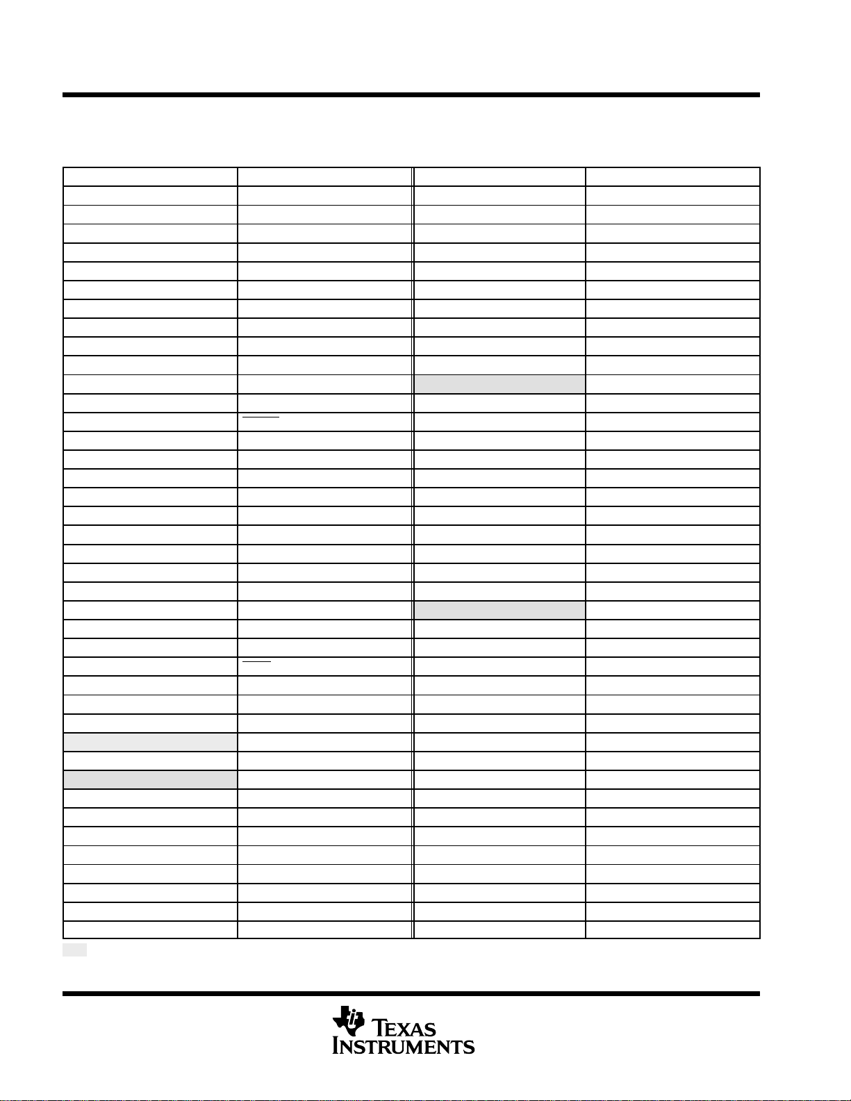
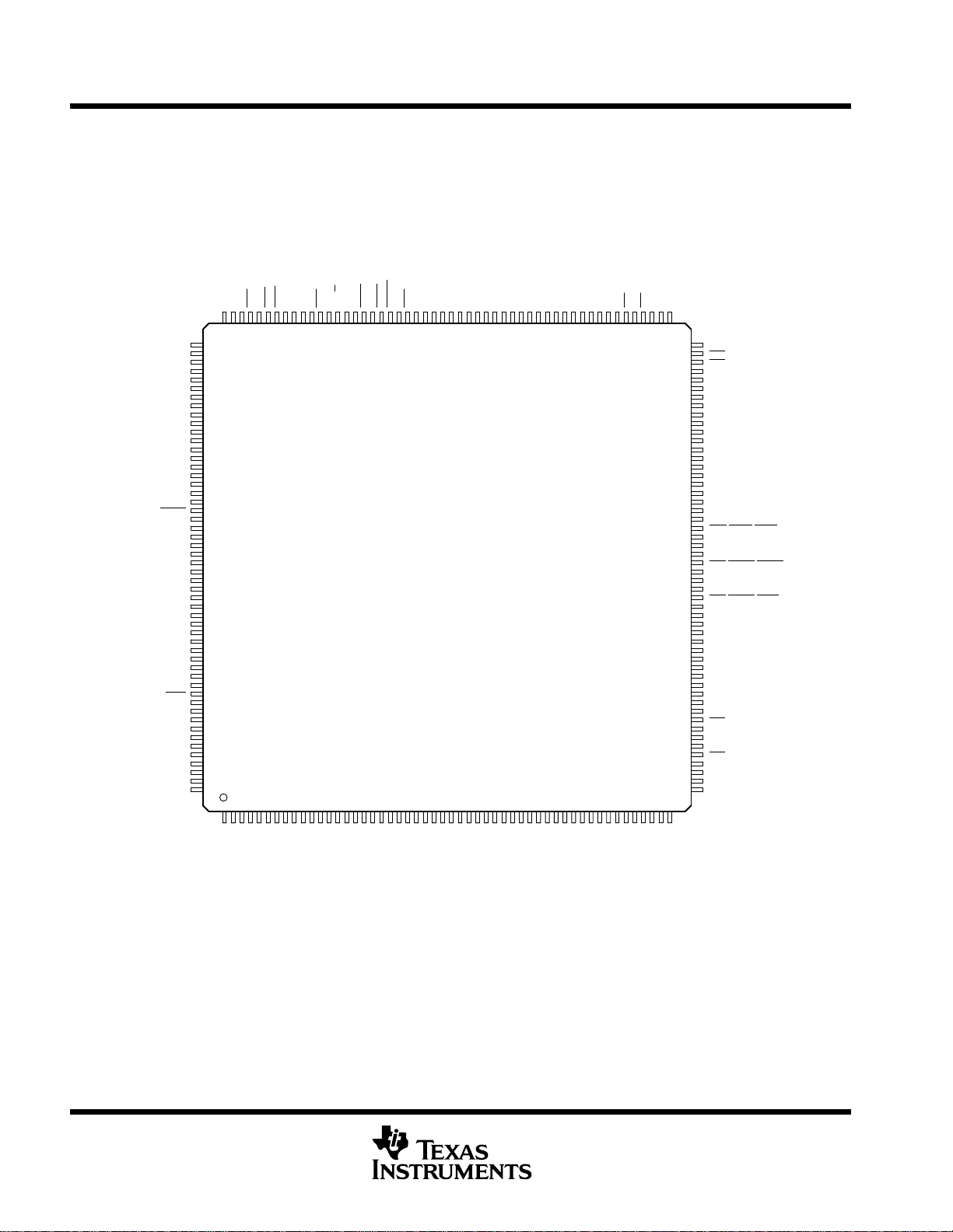
GDP 272-Ball BGA package (bottom view)
TMS320C6713, TMS320C6713B
FLOATING-POINT DIGITAL SIGNAL PROCESSORS
SPRS186I − DECEMBER 2001 − REVISED MAY 2004
V
SS
Y
V
W
V
U
T
R
P
N
M
L
K
J
CVDDDV
SS
ED19
ED20
ED22 ED21 ED23
ED24 ED25 DV
DVDDED27 ED26
ED28 ED29 ED30
SDA0 V
SCL0 ED31
CLKR1/
DR1/
AXR0[6]
SDA1
FSX1
AXR0[5]
CV
DDVSS
DR0/
DV
AXR0[0]
V
DX1/
SS
DD
ED18 BE2
DD
CV
DD
DD
FSR1/
AXR0[7]
CLKX1/
AMUTE0
CLKS0/
AHCLKR0
FSR0/
AFSR0
ED17
ED16
V
V
CV
V
V
CV
CV
V
SS
SS
DD
SS
SS
SS
DD
DD
SS
ARDY
V
SS
BE3
DVDDCVDDDV
DV
DD
CE2
EA4
CE3 EA3 EA5 EA8 EA10
DDVSS
EA7 EA9 VSSEA14 EA16 EA18 DVDDEA20EA2
EA6 DV
ECLKOUT
SDRAS
DV
DD
V
SS
V
SS
V
SS
V
SS
V
SS
AOE/
/
SSOE
CVDDCVDDDV
V
SS
V
SS
V
SS
V
SS
ECLKIN
V
SS
ARE
SDCAS/
SSADS
V
SS
V
SS
V
SS
V
SS
CLKOUT2/
/
GP[2]
DD
AWE/
SDWE/
SSWE
DDVSS
V
SS
V
SS
V
SS
V
SS
EA11
DV
DD
EA15
EA13
DV
EA12
DD
CVDDCVDDDV
V
SS
EA17
DDVSS
CE1
EA19
CV
CE0
EA21 BE1 V
V
ED13 ED15 ED14
SS
CVDDDVDDED11 ED12
V
ED9 V
SS
V
ED6 ED7 ED8
SS
V
DV
SS
CV
ED2 ED3 CV
DD
CV
ED0 ED1 V
DD
HOLD
HOLDA
DD
DD
V
SS
CV
DDVSS
DV
DD
SS
ED4 ED5
BUS
REQ
V
BE0
ED10
HINT/
GP[1]
SS
SS
DD
SS
DX0/
FSX0/
H
AFSX0
TOUT0/
G
AXR0[2]
TOUT1/
F
AXR0[4]
CLKS1/
E
SCL1
D
DV
DD
GP[5]
C
(EXT_INT5)/
AMUTEIN0
V
B
SS
V
A
SS
1 23 45 67 89 1011121314151617181920
Shading denotes the GDP package pin functions that drop out on the PYP package.
AXR0[1]
TINP0/
AXR0[3]
TINP1/
AHCLKX0
V
SS
GP[6]
(EXT_INT6)
GP[4]/
(EXT_INT4)/
AMUTEIN1
CVDDDV
V
SS
CLKR0/
ACLKR0
CLKX0/
ACLKX0
DV
DDCVDD
GP[7]
(EXT_INT7)
EMU2
CV
DD
DD
CLKIN CV
V
SS
V
SS
V
SS
V
SS
CLK
MODE0
V
SS
DD
CVDDCV
PLLHV
RSV
RSV
RSV VSSEMU0 CLKOUT3 CV
DD
CV
V
SS
TRST TMS
TCK
V
DD
SS
DV
DD
TDI TDO CVDDCV
V
EMU1
V
SS
V
SS
CV
DD
V
SS
RSV VSSCVDDCVDDDV
DD
HD14/
EMU4 RSV NMI
DV
DD
SS
EMU5
RSV
DV
RESET
DD
EMU3
DDVSS
RSV
GP[14]
HD15/
GP[15]
V
HD12/
GP[12]
HD13/
GP[13]
SS
DDVSS
HD9/
HD6/
GP[9]
AHCLKR1
HD10/
GP[10]
HD11/
GP[11]
HD8/
GP[8]
DV
DD
V
SS
DV
DD
HCNTL0/
AXR1[3]
HDS2/
AXR1[5]
HAS/
ACLKX1
HD2/
AFSX1
CV
DD
HD5/
AHCLKX1
HD7/
GP[3]
HRDY/
ACLKR1
HCNTL1/
AXR1[1]
V
SS
HDS1/
AXR1[6]
DV
DD
HD4/
GP[0]
CV
DDVSS
V
SS
HHWIL/
AFSR1
HR/W/
AXR1[0]
HCS/
AXR1[2]
HD0/
AXR1[4]
HD1/
AXR1[7]
HD3/
AMUTE1
V
SS
POST OFFICE BOX 1443 • HOUSTON, TEXAS 77251−1443
3
Page 4
TMS320C6713, TMS320C6713B
FLOATING-POINT DIGITAL SIGNAL PROCESSORS
SPRS186I − DECEMBER 2001 − REVISED MAY 2004
GDP 272-Ball BGA package (bottom view) (continued)
Table 1. Terminal Assignments for the 272-Ball GDP Package (in Order of Ball No.)
BALL NO. SIGNAL NAME BALL NO. SIGNAL NAME
A1 V
A2 V
A3 CLKIN C3 CV
A4 CV
A5 RSV C5 PLLHV
A6 TCK C6 V
A7 TDI C7 CV
A8 TDO C8 V
A9 CV
A10 CV
A11 V
A12 RSV C12 RSV
A13 RESET C13 NMI
A14 V
A15 HD13/GP[13] C15 HD12/GP[12]
A16 HD11/GP[11] C16 HD9/GP[9]
A17 DV
A18 HD7/GP[3] C18 CV
A19 V
A20 V
B1 V
B2 CV
B3 DV
B4 V
B5 RSV D5 CV
B6 TRST D6 CV
B7 TMS D7 RSV
B8 DV
B9 EMU1 D9 EMU0
B10 EMU3 D10 CLKOUT3
B11 RSV D11 CV
B12 EMU5 D12 RSV
B13 DV
B14 HD15/GP[15] D14 CV
B15 V
B16 HD10/GP[10] D16 DV
B17 HD8/GP[8] D17 V
B18 HD5/AHCLKX1 D18 HD2/AFSX1
B19 CV
B20 V
Shading denotes the GDP package pin functions that drop out on the PYP package.
SS
SS
DD
DD
DD
SS
SS
DD
SS
SS
SS
DD
DD
SS
DD
DD
SS
DD
SS
C1 GP[5](EXT_INT5)/AMUTEIN0
C2 GP[4](EXT_INT4)/AMUTEIN1
DD
C4 CLKMODE0
SS
DD
SS
C9 V
C10 DV
SS
DD
C11 EMU4
C14 HD14/GP[14]
C17 HD6/AHCLKR1
DD
C19 HD4/GP[0]
C20 HD3/AMUTE1
D1 DV
DD
D2 GP[6](EXT_INT6)
D3 EMU2
D4 V
D8 V
D13 V
D15 CV
D19 DV
SS
DD
DD
SS
DD
SS
DD
DD
DD
SS
DD
D20 HD1/AXR1[7]
4
POST OFFICE BOX 1443 • HOUSTON, TEXAS 77251−1443
Page 5
TMS320C6713, TMS320C6713B
FLOATING-POINT DIGITAL SIGNAL PROCESSORS
SPRS186I − DECEMBER 2001 − REVISED MAY 2004
Table 1. Terminal Assignments for the 272-Ball GDP Package (in Order of Ball No.) (Continued)
BALL NO. SIGNAL NAME BALL NO. SIGNAL NAME
E1 CLKS1/SCL1 J17 HOLD
E2 V
SS
E3 GP[7](EXT_INT7) J19 BUSREQ
E4 V
E17 V
SS
SS
E18 HAS/ACLKX1 K2 V
E19 HDS1/AXR1[6] K3 CLKS0/AHCLKR0
E20 HD0/AXR1[4] K4 CV
F1 TOUT1/AXR0[4] K9 V
F2 TINP1/AHCLKX0 K10 V
F3 DV
F4 CV
F17 CV
DD
DD
DD
F18 HDS2/AXR1[5] K18 ED0
F19 V
SS
F20 HCS/AXR1[2] K20 V
G1 TOUT0/AXR0[2] L1 FSX1
G2 TINP0/AXR0[3] L2 DX1/AXR0[5]
G3 CLKX0/ACLKX0 L3 CLKX1/AMUTE0
G4 V
G17 V
SS
SS
G18 HCNTL0/AXR1[3] L10 V
G19 HCNTL1/AXR1[1] L11 V
G20 HR/W/AXR1[0] L12 V
H1 FSX0/AFSX0 L17 CV
H2 DX0/AXR0[1] L18 ED2
H3 CLKR0/ACLKR0 L19 ED3
H4 V
H17 V
H18 DV
SS
SS
DD
H19 HRDY/ACLKR1 M3 FSR1/AXR0[7]
H20 HHWIL/AFSR1 M4 V
J1 DR0/AXR0[0] M9 V
J2 DV
DD
J3 FSR0/AFSR0 M11 V
J4 V
J9 V
J10 V
J11 V
J12 V
SS
SS
SS
SS
SS
Shading denotes the GDP package pin functions that drop out on the PYP package.
J18 HOLDA
J20 HINT/GP[1]
K1 CV
K11 V
K12 V
K17 CV
DD
SS
DD
SS
SS
SS
SS
DD
K19 ED1
SS
L4 CV
L9 V
L20 CV
DD
SS
SS
SS
SS
DD
DD
M1 CLKR1/AXR0[6]
M2 DR1/SDA1
SS
SS
M10 V
M12 V
M17 V
M18 DV
SS
SS
SS
SS
DD
M19 ED4
M20 ED5
POST OFFICE BOX 1443 • HOUSTON, TEXAS 77251−1443
5
Page 6
TMS320C6713, TMS320C6713B
FLOATING-POINT DIGITAL SIGNAL PROCESSORS
SPRS186I − DECEMBER 2001 − REVISED MAY 2004
Table 1. Terminal Assignments for the 272-Ball GDP Package (in Order of Ball No.) (Continued)
BALL NO. SIGNAL NAME BALL NO. SIGNAL NAME
N1 SCL0 U9 V
N2 SDA0 U10 CV
N3 ED31 U11 CV
N4 V
N17 V
SS
SS
U12 DV
U13 V
N18 ED6 U14 CV
N19 ED7 U15 CV
N20 ED8 U16 DV
P1 ED28 U17 V
P2 ED29 U18 EA21
P3 ED30 U19 BE1
P4 V
P17 V
SS
SS
U20 V
P18 ED9 V2 ED19
P19 V
SS
P20 ED10 V4 ED16
R1 DV
DD
R2 ED27 V6 CE3
R3 ED26 V7 EA3
R4 CV
R17 CV
R18 DV
DD
DD
DD
V10 EA10
R19 ED11 V11 ARE/SDCAS/SSADS
R20 ED12 V12 AWE/SDWE/SSWE
T1 ED24 V13 DV
T2 ED25 V14 EA12
T3 DV
T4 V
T17 V
DD
SS
SS
V15 DV
V16 EA17
V17 CE0
T18 ED13 V18 CV
T19 ED15 V19 DV
T20 ED14 V20 BE0
U1 ED22 W1 V
U2 ED21 W2 CV
U3 ED23 W3 DV
U4 V
U5 DV
U6 CV
U7 DV
U8 V
SS
DD
DD
DD
SS
Shading denotes the GDP package pin functions that drop out on the PYP package.
V1 ED20
V3 CV
V5 BE3
V8 EA5
V9 EA8
W4 ED17
W5 V
W6 CE2
W7 EA4
W8 EA6
SS
DD
DD
DD
SS
DD
DD
DD
SS
SS
DD
DD
DD
DD
DD
SS
DD
DD
SS
6
POST OFFICE BOX 1443 • HOUSTON, TEXAS 77251−1443
Page 7
TMS320C6713, TMS320C6713B
FLOATING-POINT DIGITAL SIGNAL PROCESSORS
SPRS186I − DECEMBER 2001 − REVISED MAY 2004
Table 1. Terminal Assignments for the 272-Ball GDP Package (in Order of Ball No.) (Continued)
BALL NO. SIGNAL NAME BALL NO. SIGNAL NAME
W9 DV
DD
W10 AOE/SDRAS/SSOE Y6 EA2
W11 V
W12 DV
SS
DD
W13 EA11 Y9 EA9
W14 EA13 Y10 ECLKOUT
W15 EA15 Y11 ECLKIN
W16 V
SS
W17 EA19 Y13 V
W18 CE1 Y14 EA14
W19 CV
W20 V
Y1 V
Y2 V
DD
SS
SS
SS
Y3 ED18 Y19 V
Y4 BE2 Y20 V
Shading denotes the GDP package pin functions that drop out on the PYP package.
Y5 ARDY
Y7 DV
DD
Y8 EA7
Y12 CLKOUT2/GP[2]
SS
Y15 EA16
Y16 EA18
Y17 DV
DD
Y18 EA20
SS
SS
POST OFFICE BOX 1443 • HOUSTON, TEXAS 77251−1443
7
Page 8
TMS320C6713, TMS320C6713B
FLOATING-POINT DIGITAL SIGNAL PROCESSORS
SPRS186I − DECEMBER 2001 − REVISED MAY 2004
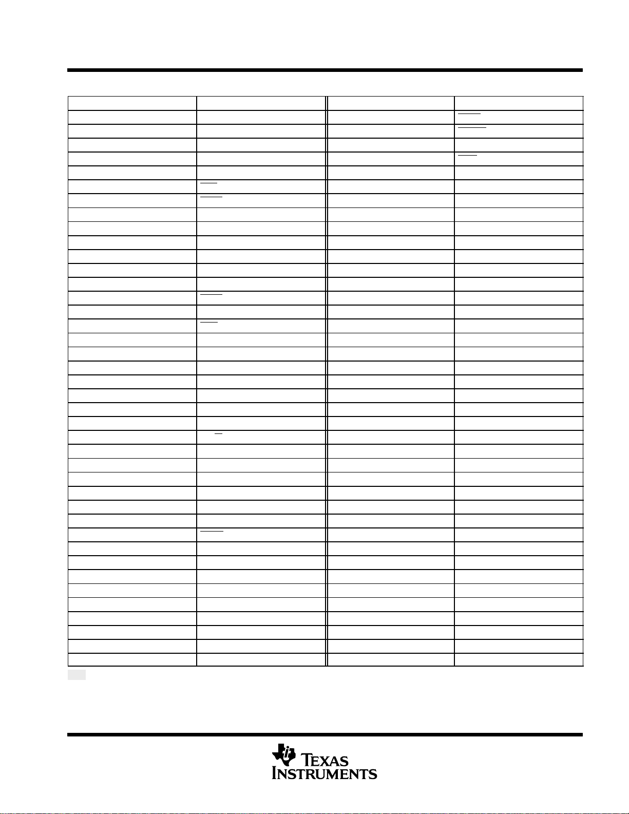
PYP PowerPAD QFP package (top view)
CV
V
HD5/AHCLKX1
HD8/GP[8]
HD6/AHCLKR1
DV
V
HD7/GP[3]
HD9/GP[9]
HD10/GP[10]
HD11/GP[11]
HD12/GP[12]
CV
V
CV
HD13/GP[13]
HD14/GP[14]
HD15/GP[15]
NMI
RESET
CV
RSV
RSV
RSV
RSV
V
DV
CLKOUT3
EMU1
EMU0
TDO
DV
V
CV
TDI
TMS
TCK
V
CV
CV
TRST
RSV
V
RSV
CV
PLLHV
CLKIN
CLKMODE0
DV
V
CV
PYP 208-PIN PowerPAD PLASTIC QUAD FLATPACK (PQFP)
( TOP VIEW )
SS
V
HCS/AXR1[2]
HD0/AXR1[4]
HCNTL0/AXR1[3]
148
147
146
145
W/AXR1[0]
DD
SS
HCNTL1/AXR1[1]
HR/
V
DV
144
143
142
141
DD
HAS/ACLKX1
HDS1/AXR1[6]
HD3/AMUTE1
HD1/AXR1[7]
154
153
152
151
150
HDS2/AXR1[5]
CV
149
HD4/GP[0]
HD2/AFSX1
156
155
157
DD
158
SS
159
160
161
162
DD
163
SS
164
165
166
167
168
169
DD
SS
170
DD
171
172
173
174
175
176
177
DD
178
179
180
181
182
SS
DD
183
184
185
186
187
188
DD
SS
189
DD
190
191
192
193
SS
194
DD
195
DD
196
197
198
SS
199
200
DD
201
202
V
SS
203
204
205
206
DD
207
SS
208
DD
1234567891011121314151617181920212223242526272829303132333435363738394041
HRDY/ACLKR1
HOLDA
HOLD
HHWIL/AFSR1
140
139
138
137
/GP[1]
BUSREQ
HINT
V
136
135
134
110
BE0
EA21
109
BE1
108
DD
DD
SS
CV
V
DV
107
106
105
CV
DD
104
CE1
103
CE0
102
101
EA20
100
EA19
EA17
99
DV
DD
98
V
97
SS
CV
96
DD
EA18
95
EA15
94
EA12
93
EA16
92
EA13
91
EA14
90
CV
89
DD
V
88
SS
DV
87
DD
EA11
86
V
SS
85
DV
DD
84
AWE/SDWE/SSWE
83
CLKOUT2/GP[2]
82
V
SS
81
CV
DD
80
ARE/SDCAS/SSADS
79
ECLKIN
78
ECLKOUT
77
EA10
76
AOE/SDRAS/SSOE
75
EA9
74
V
SS
73
DV
DD
72
EA8
71
EA7
70
EA6
69
EA5
68
CV
67
DD
V
SS
66
DV
DD
65
EA4
64
EA3
63
EA2
62
CE2
61
CV
DD
60
V
SS
59
DV
DD
58
CE3
57
ARDY
56
DV
DD
55
V
SS
54
CV
DD
53
52
DD
SS
ED0
ED1
ED2
CV
133
132
131
130
ED3
129
ED5
128
ED4
127
DV
126
DD
DD
SS
ED8
ED7
CV
V
125
124
123
122
ED6
121
ED10
120
ED9
119
ED12
118
ED11
117
DD
DD
SS
ED14
ED15
ED13
CV
V
DV
111
116
115
114
113
112
434445464748495051
42
SS
DD
DD
V
DV
CV
CLKS1/SCL1
GP[6](EXT_INT6)
GP[7](EXT_INT7)
GP[5](EXT_INT5)/AMUTEIN0
GP[4](EXT_INT4)/AMUTEIN1
8
DD
DD
DV
DD
SS
V
CV
TOUT1/AXR0[4]
TINP1/AHCLKX0
SS
V
CV
CLKX0/ACLKX0
DX0/AXR0[1]
TINP0/AXR0[3]
TOUT0/AXR0[2]
CLKR0/ACLKR0
POST OFFICE BOX 1443 • HOUSTON, TEXAS 77251−1443
DDCVDD
SS
V
FSX0/AFSX0
FSR0/AFSR0
SS
V
DV
DR0/AXR0[0]
SS
DD
V
FSX1
CV
DX1/AXR0[5]
CLKX1/AMUTE0
CLKS0/AHCLKR0
SS
DD
V
CV
DR1/SDA1
CLKR1/AXR0[6]
SS
DDCVDDCVDD
V
SCL0
SDA0
FSR1/AXR0[7]
DD
DD
DV
DD
DD
SS
SS
SS
V
CV
SS
V
V
V
CV
CV
DV
Page 9

TMS320C6713, TMS320C6713B
FLOATING-POINT DIGITAL SIGNAL PROCESSORS
SPRS186I − DECEMBER 2001 − REVISED MAY 2004
description
The TMS320C67xt DSPs (including the TMS320C6713 and TMS320C6713B devices†) compose the
floating-point DSP generation in the TMS320C6000t DSP platform. The C6713 and C6713B devices are
based on the high-performance, advanced very-long-instruction-word (VLIW) architecture developed by Texas
Instruments (TI), making this DSP an excellent choice for multichannel and multifunction applications.
Operating at 225 MHz, the C6713/13B delivers up to 1350 million floating-point operations per second
(MFLOPS), 1800 million instructions per second (MIPS), and with dual fixed-/floating-point multipliers up to 450
million multiply-accumulate operations per second (MMACS).
Operating at 300 MHz, the C6713B delivers up to 1800 million floating-point operations per second (MFLOPS),
2400 million instructions per second (MIPS), and with dual fixed-/floating-point multipliers up to 600 million
multiply-accumulate operations per second (MMACS).
The C6713/13B uses a two-level cache-based architecture and has a powerful and diverse set of peripherals.
The Level 1 program cache (L1P) is a 4K-Byte direct-mapped cache and the Level 1 data cache (L1D) is a
4K-Byte 2-way set-associative cache. The Level 2 memory/cache (L2) consists of a 256K-Byte memory space
that is shared between program and data space. 64K Bytes of the 256K Bytes in L2 memory can be configured
as mapped memory, cache, or combinations of the two. The remaining 192K Bytes in L2 serves as mapped
SRAM.
The C6713/13B has a rich peripheral set that includes two Multichannel Audio Serial Ports (McASPs), two
Multichannel Buffered Serial Ports (McBSPs), two Inter-Integrated Circuit (I2C) buses, one dedicated
General-Purpose Input/Output (GPIO) module, two general-purpose timers, a host-port interface (HPI), and a
glueless external memory interface (EMIF) capable of interfacing to SDRAM, SBSRAM, and asynchronous
peripherals.
The two McASP interface modules each support one transmit and one receive clock zone. Each of the McASP
has eight serial data pins which can be individually allocated to any of the two zones. The serial port supports
time-division multiplexing on each pin from 2 to 32 time slots. The C6713/13B has sufficient bandwidth to
support all 16 serial data pins transmitting a 192 kHz stereo signal. Serial data in each zone may be transmitted
and received on multiple serial data pins simultaneously and formatted in a multitude of variations on the Philips
Inter-IC Sound (I2S) format.
In addition, the McASP transmitter may be programmed to output multiple S/PDIF, IEC60958, AES-3, CP-430
encoded data channels simultaneously, with a single RAM containing the full implementation of user data and
channel status fields.
The McASP also provides extensive error-checking and recovery features, such as the bad clock detection
circuit for each high-frequency master clock which verifies that the master clock is within a programmed
frequency range.
The two I2C ports on the TMS320C6713/13B allow the DSP to easily control peripheral devices and
communicate with a host processor. In addition, the standard multichannel buffered serial port (McBSP) may
be used to communicate with serial peripheral interface (SPI) mode peripheral devices.
The TMS320C6713/13B device has two bootmodes: from the HPI or from external asynchronous ROM. For
more detailed information, see the bootmode section of this data sheet.
The TMS320C67x DSP generation is supported by the TI eXpressDSPt set of industry benchmark
development tools, including a highly optimizing C/C++ Compiler, the Code Composer Studiot Integrated
Development Environment (IDE), JTAG-based emulation and real-time debugging, and the DSP/BIOSt
kernel.
TMS320C6000, eXpressDSP, Code Composer Studio, and DSP/BIOS are trademarks of Texas Instruments.
†
Throughout the remainder of this document, the TMS320C6713 and TMS320C6713B shall be referred to as TMS320C67x or C67x or 13/13B
where generic, and where specific, their individual full device part numbers will be used or abbreviated as C6713, C6713B, 13, or 13B, etc.
POST OFFICE BOX 1443 • HOUSTON, TEXAS 77251−1443
9
Page 10
TMS320C6713, TMS320C6713B
HARDWARE FEATURES
Peripherals
Not all
available at the same
g
Configuration section.)
dependent on chip-level
Voltage
FLOATING-POINT DIGITAL SIGNAL PROCESSORS
SPRS186I − DECEMBER 2001 − REVISED MAY 2004
device characteristics
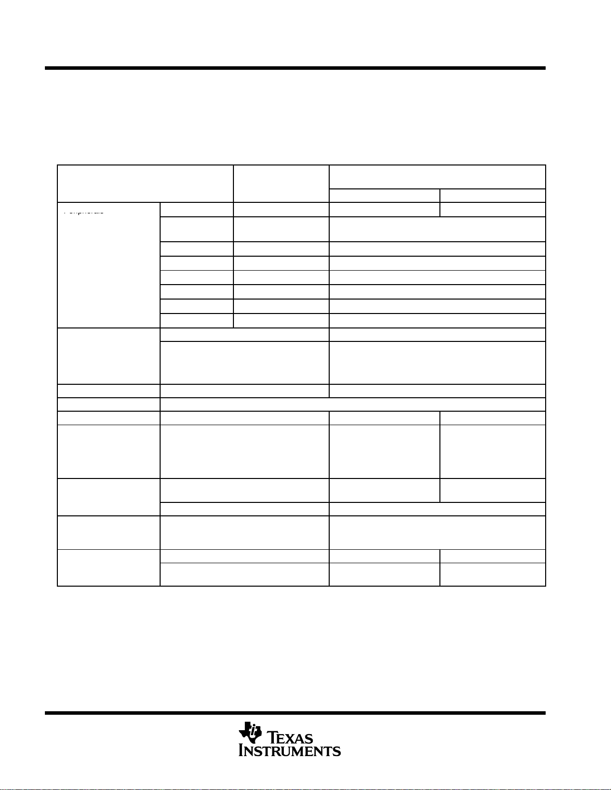
Table 2 provides an overview of the C6713/C6713B DSPs. The table shows significant features of the each
device, including the capacity of on-chip RAM, the peripherals, the execution time, and the package type with
pin count. For more details on the C67x DSP device part numbers and part numbering, see Table 24 and
Figure 12.
Table 2. Characteristics of the C6713 and C6713B Processors
HARDWARE FEATURES
Peripherals
peripheral pins are
available at the same
time. (For more details,
see the Device
Confi
uration section.)
Peripheral performance is
nn n hi-lv
configuration.
On-Chip Memory
CPU ID+CPU Rev ID Control Status Register (CSR.[31:16]) 0x0203
BSDL File For the C6713/13B BSDL file, contact your Field Sales Representative.
Frequency MHz 300, 225, 200 200, 167
Cycle Time ns
Voltage
Clock Generator Options
Packages
†
PRODUCT PREVIEW information concerns products in the formative or design phase of development. Characteristic data and
other specifications are design goals. Texas Instruments reserves the right to change or discontinue these products without
notice.
ADVANCE INFORMATION concerns new products in the sampling or preproduction phase of development. Characteristic data
and other specifications are subject to change without notice.
PRODUCTION DATA information is current as of publication date. Products conform to specifications per the terms of Texas
Instruments standard warranty. Production processing does not necessarily include testing of all parameters.
‡
AUXCLK is the McASP internal high-frequency clock source for serial transfers. SYSCLK2 is the McASP system clock used
for the clock check (high-frequency) circuit.
§
This value is compatible with existing 1.26V designs.
EMIF SYSCLK3 or ECLKIN 1 (32 bit) 1 (16 bit)
EDMA
(16 Channels)
HPI (16 bit) SYSCLK2 1
McASPs AUXCLK, SYSCLK2
I2Cs SYSCLK2 2
McBSPs SYSCLK2 2
32-Bit Timers 1/2 of SYSCLK2 2
l
GPIO Module SYSCLK2 1
Size (Bytes) 264K
Organization
Core (V)
I/O (V) 3.3 V
Prescaler
Multiplier
Postscaler
27 x 27 mm 272-Ball BGA (GDP) −
28 x 28 mm −
INTERNAL CLOCK
SOURCE
CPU clock frequency 1
‡
3.3 ns (C6713BGDP-300)
4.4 ns (C6713BGDP-225)
5 ns (C6713BGDPA-200)
4.4 ns (C6713GDP-225)
5 ns (C6713GDPA-200)
1.20§ V (C6713/C6713B)
GDP PYP
1.4 V (C6713B−300)
C6713/C6713B
(FLOATING-POINT DSPs)
2
4K-Byte (4KB) L1 Program (L1P) Cache
4KB L1 Data (L1D) Cache
64KB Unified L2 Cache/Mapped RAM
192KB L2 Mapped RAM
5 ns (C6713BPYP-200)
6 ns (C6713BPYPA-167)
5 ns (C6713PYP-200)
6 ns (C6713PYPA-167)
1.2 V
/1, /2, /3, ..., /32
x4, x5, x6, ..., x25
/1, /2, /3, ..., /32
208-Pin PowerPAD
PQFP (PYP)
C67x is a trademark of Texas Instruments.
10
POST OFFICE BOX 1443 • HOUSTON, TEXAS 77251−1443
Page 11

TMS320C6713, TMS320C6713B
FLOATING-POINT DIGITAL SIGNAL PROCESSORS
SPRS186I − DECEMBER 2001 − REVISED MAY 2004
Table 2. Characteristics of the C6713 and C6713B Processors (Continued)
HARDWARE FEATURES
Process Technology µm 0.13
Product Status
†
PRODUCT PREVIEW information concerns products in the formative or design phase of development. Characteristic data and
other specifications are design goals. Texas Instruments reserves the right to change or discontinue these products without
notice.
ADVANCE INFORMATION concerns new products in the sampling or preproduction phase of development. Characteristic data
and other specifications are subject to change without notice.
PRODUCTION DATA information is current as of publication date. Products conform to specifications per the terms of Texas
Instruments standard warranty. Production processing does not necessarily include testing of all parameters.
‡
AUXCLK is the McASP internal high-frequency clock source for serial transfers. SYSCLK2 is the McASP system clock used
for the clock check (high-frequency) circuit.
†
Product Preview (PP)
Advance Information (AI)
Production Data (PD)
INTERNAL CLOCK
SOURCE
PD (13) PD (13, 13B)
C6713/C6713B
(FLOATING-POINT DSPs)
POST OFFICE BOX 1443 • HOUSTON, TEXAS 77251−1443
11
Page 12
TMS320C6713, TMS320C6713B
FLOATING-POINT DIGITAL SIGNAL PROCESSORS
SPRS186I − DECEMBER 2001 − REVISED MAY 2004
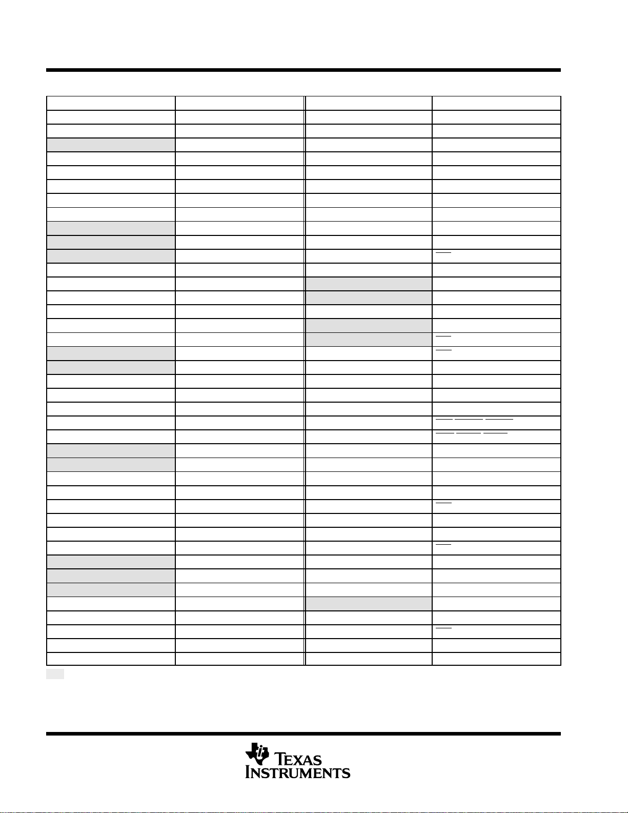
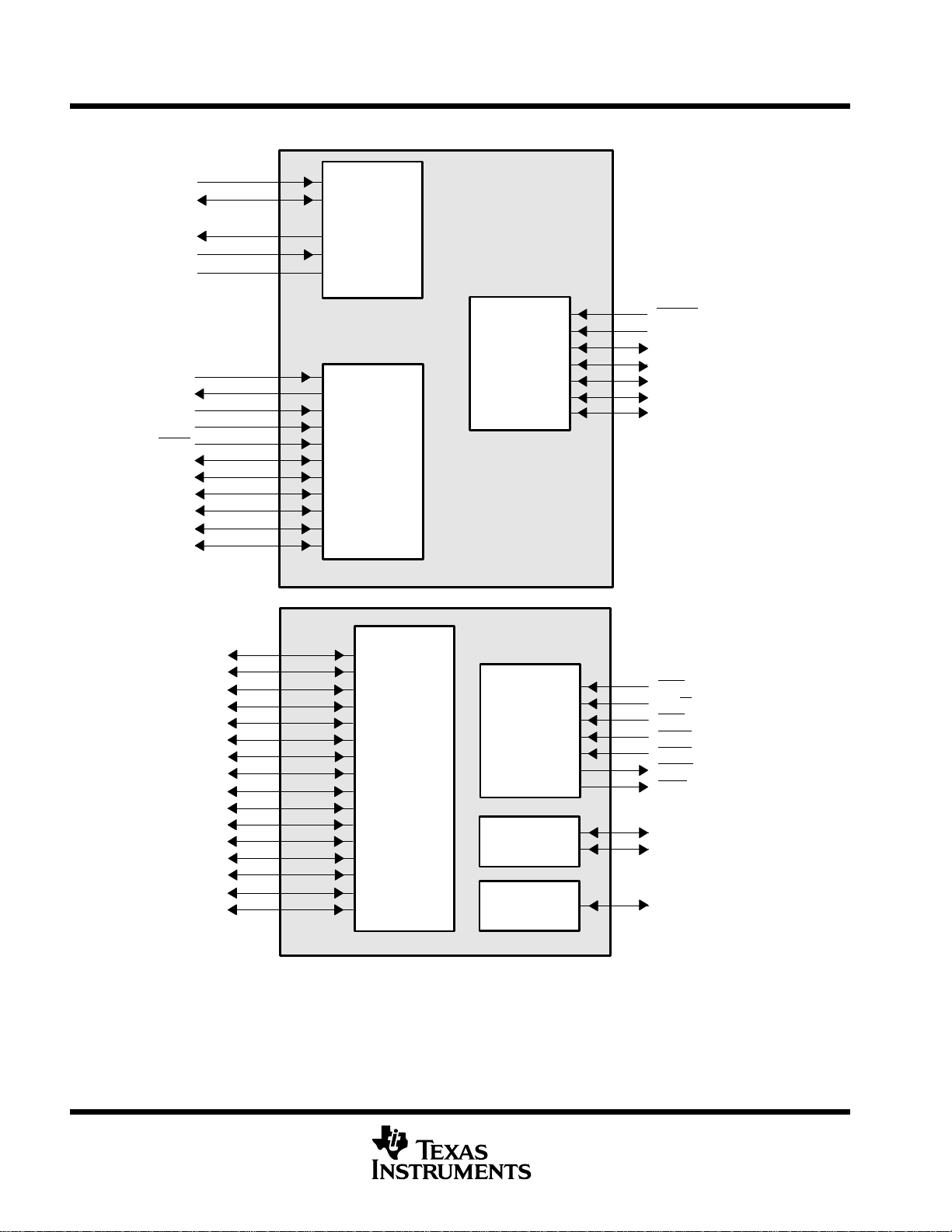
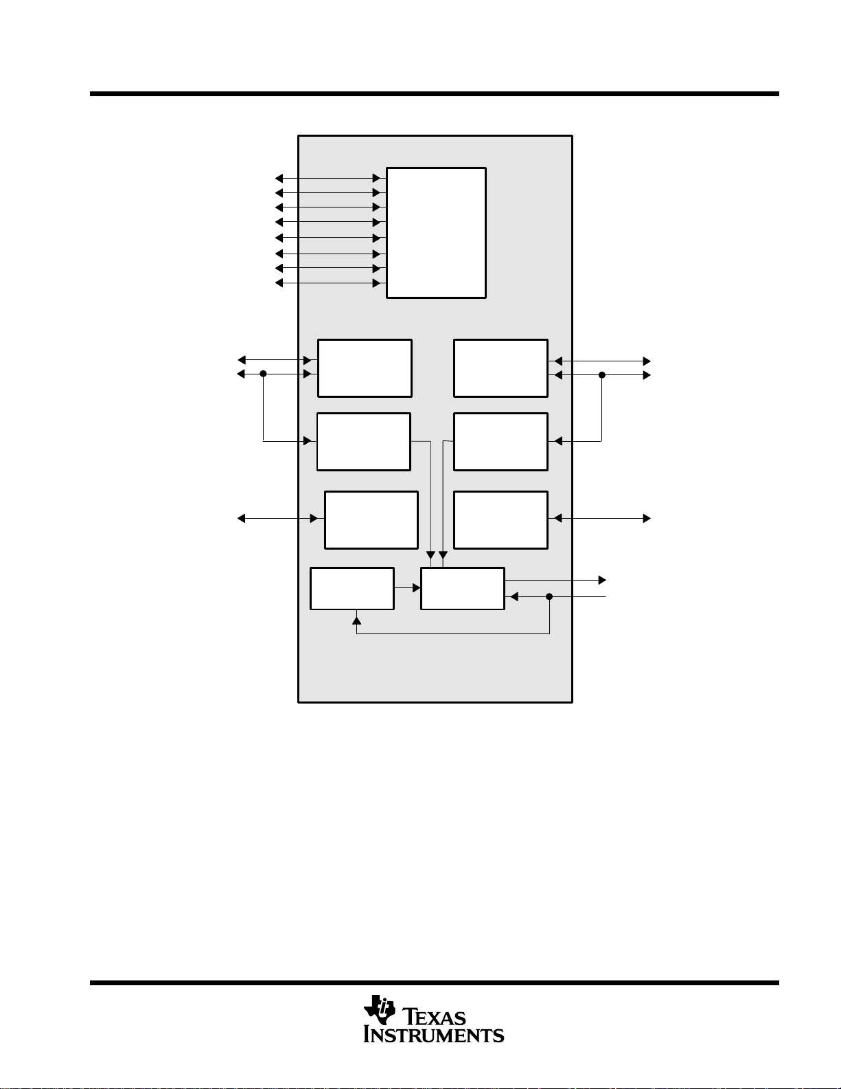
functional block and CPU (DSP core) diagram
C6713/13B Digital Signal Processors
32
Pin Multiplexing
EMIF
McASP1
McASP0
McBSP1
McBSP0
I2C1
I2C0
Timer 1
Timer 0
Enhanced
DMA
Controller
(16 channel)
L2 Cache/
Memory
4 Banks
64K Bytes
Total
(up to
4-Way)
L2
Memory
192K
Bytes
L1P Cache
Direct Mapped
4K Bytes Total
C67x CPU
Instruction Fetch
Instruction Dispatch
Instruction Decode
Data Path A
A Register File
.L1†.S1†.M1†.D1 .D2 .M2†.S2†.L2
Clock Generator and PLL
x4 through x25 Multiplier
/1 through /32 Dividers
Data Path B
B Register File
L1D Cache
2-Way
Set Associative
4K Bytes
Power-Down
Control
Registers
Control
In-Circuit
Emulation
Interrupt
†
Control
Logic
Logic
Test
GPIO
16
†
In addition to fixed-point instructions, these functional units execute floating-point instructions.
EMIF interfaces to:
−SDRAM
−SBSRAM
−SRAM,
−ROM/Flash, and
HPI
McBSPs interface to:
−SPI Control Port
−High-Speed TDM Codecs
−AC97 Codecs
−Serial EEPROM
McASPs interface to:
−I2S Multichannel ADC, DAC, Codec, DIR
−DIT: Multiple Outputs
−I/O devices
12
POST OFFICE BOX 1443 • HOUSTON, TEXAS 77251−1443
Page 13

TMS320C6713, TMS320C6713B
FLOATING-POINT DIGITAL SIGNAL PROCESSORS
SPRS186I − DECEMBER 2001 − REVISED MAY 2004
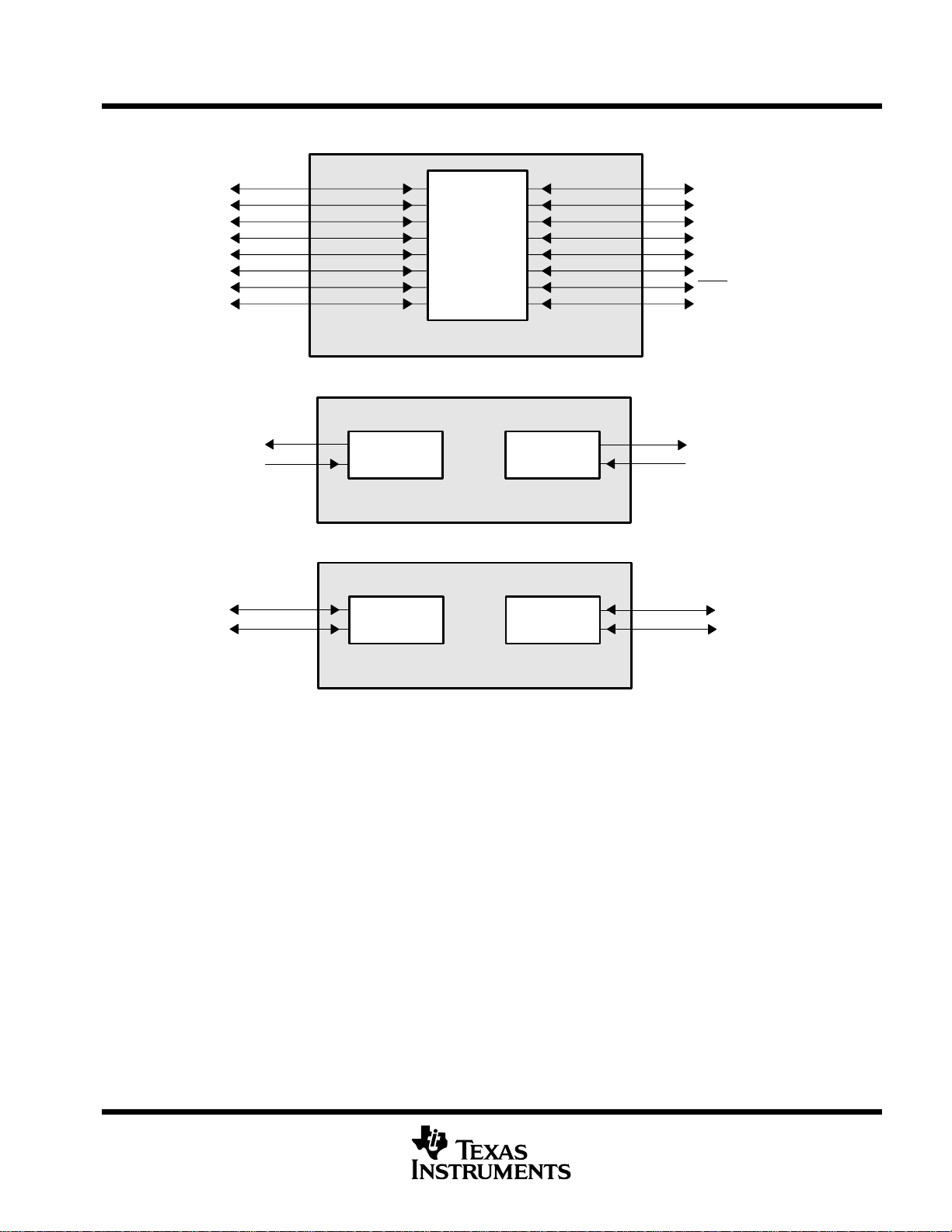
CPU (DSP core) description
The TMS320C6713/13B floating-point digital signal processor is based on the C67x CPU. The CPU fetches
advanced very-long instruction words (VLIW) (256 bits wide) to supply up to eight 32-bit instructions to the eight
functional units during every clock cycle. The VLIW architecture features controls by which all eight units do not
have to be supplied with instructions if they are not ready to execute. The first bit of every 32-bit instruction
determines if the next instruction belongs to the same execute packet as the previous instruction, or whether
it should be executed in the following clock as a part of the next execute packet. Fetch packets are always 256
bits wide; however, the execute packets can vary in size. The variable-length execute packets are a key
memory-saving feature, distinguishing the C67x CPU from other VLIW architectures.
The CPU features two sets of functional units. Each set contains four units and a register file. One set contains
functional units .L1, .S1, .M1, and .D1; the other set contains units .D2, .M2, .S2, and .L2. The two register files
each contain 16 32-bit registers for a total of 32 general-purpose registers. The two sets of functional units, along
with two register files, compose sides A and B of the CPU (see the functional block and CPU diagram and
Figure 1). The four functional units on each side of the CPU can freely share the 16 registers belonging to that
side. Additionally, each side features a single data bus connected to all the registers on the other side, by which
the two sets of functional units can access data from the register files on the opposite side. While register access
by functional units on the same side of the CPU as the register file can service all the units in a single clock cycle,
register access using the register file across the CPU supports one read and one write per cycle.
The C67x CPU executes all C62x instructions. In addition to C62x fixed-point instructions, the six out of eight
functional units (.L1, .S1, .M1, .M2, .S2, and .L2) also execute floating-point instructions. The remaining two
functional units (.D1 and .D2) also execute the new LDDW instruction which loads 64 bits per CPU side for a
total of 128 bits per cycle.
Another key feature of the C67x CPU is the load/store architecture, where all instructions operate on registers
(as opposed to data in memory). Two sets of data-addressing units (.D1 and .D2) are responsible for all data
transfers between the register files and the memory. The data address driven by the .D units allows data
addresses generated from one register file to be used to load or store data to or from the other register file. The
C67x CPU supports a variety of indirect addressing modes using either linear- or circular-addressing modes
with 5- or 15-bit offsets. All instructions are conditional, and most can access any one of the 32 registers. Some
registers, however, are singled out to support specific addressing or to hold the condition for conditional
instructions (if the condition is not automatically “true”). The two .M functional units are dedicated for multiplies.
The two .S and .L functional units perform a general set of arithmetic, logical, and branch functions with results
available every clock cycle.
The processing flow begins when a 256-bit-wide instruction fetch packet is fetched from a program memory.
The 32-bit instructions destined for the individual functional units are “linked” together by “1” bits in the least
significant bit (LSB) position of the instructions. The instructions that are “chained” together for simultaneous
execution (up to eight in total) compose an execute packet. A “0” in the LSB of an instruction breaks the chain,
effectively placing the instructions that follow it in the next execute packet. If an execute packet crosses the
fetch-packet boundary (256 bits wide), the assembler places it in the next fetch packet, while the remainder of
the current fetch packet is padded with NOP instructions. The number of execute packets within a fetch packet
can vary from one to eight. Execute packets are dispatched to their respective functional units at the rate of one
per clock cycle and the next 256-bit fetch packet is not fetched until all the execute packets from the current fetch
packet have been dispatched. After decoding, the instructions simultaneously drive all active functional units
for a maximum execution rate of eight instructions every clock cycle. While most results are stored in 32-bit
registers, they can be subsequently moved to memory as bytes or half-words as well. All load and store
instructions are byte-, half-word, or word-addressable.
POST OFFICE BOX 1443 • HOUSTON, TEXAS 77251−1443
13
Page 14
TMS320C6713, TMS320C6713B
FLOATING-POINT DIGITAL SIGNAL PROCESSORS
SPRS186I − DECEMBER 2001 − REVISED MAY 2004
CPU (DSP core) description (continued)
†
.L1
long dst
long src
LD1 32 MSB
Data Path A
ST1
LD1 32 LSB
DA1
.S1
.M1
.D1
long src
long dst
†
†
src1
src2
dst
dst
src1
src2
dst
src1
src2
dst
src1
src2
8
8
8
8
32
32
Register
File A
(A0−A15)
2X
Data Path B
DA2
LD2 32 LSB
LD2 32 MSB
ST2
.D2
.M2
.S2
.L2
src2
src1
dst
src2
†
src1
dst
src2
src1
†
dst
long dst
long src
long src
long dst
dst
†
src2
src1
1X
Register
File B
8
8
32
32
8
8
(B0−B15)
Control
Register File
†
In addition to fixed-point instructions, these functional units execute floating-point instructions.
Figure 1. TMS320C67x CPU (DSP Core) Data Paths
14
POST OFFICE BOX 1443 • HOUSTON, TEXAS 77251−1443
Page 15
TMS320C6713, TMS320C6713B
FLOATING-POINT DIGITAL SIGNAL PROCESSORS
SPRS186I − DECEMBER 2001 − REVISED MAY 2004
memory map summary
Table 3 shows the memory map address ranges of the C6713/13B devices.
Table 3. TMS320C6713/13B Memory Map Summary
MEMORY BLOCK DESCRIPTION BLOCK SIZE (BYTES) HEX ADDRESS RANGE
Internal RAM (L2) 192K 0000 0000 – 0002 FFFF
Internal RAM/Cache 64K 0003 0000 – 0003 FFFF
Reserved 24M – 256K 0004 0000 – 017F FFFF
External Memory Interface (EMIF) Registers 256K 0180 0000 – 0183 FFFF
L2 Registers 128K 0184 0000 – 0185 FFFF
Reserved 128K 0186 0000 – 0187 FFFF
HPI Registers 256K 0188 0000 – 018B FFFF
McBSP 0 Registers 256K 018C 0000 – 018F FFFF
McBSP 1 Registers 256K 0190 0000 – 0193 FFFF
Timer 0 Registers 256K 0194 0000 – 0197 FFFF
Timer 1 Registers 256K 0198 0000 – 019B FFFF
Interrupt Selector Registers 512 019C 0000 – 019C 01FF
Device Configuration Registers 4 019C 0200 – 019C 0203
Reserved 256K − 516 019C 0204 – 019F FFFF
EDMA RAM and EDMA Registers 256K 01A0 0000 – 01A3 FFFF
Reserved 768K 01A4 0000 – 01AF FFFF
GPIO Registers 16K 01B0 0000 – 01B0 3FFF
Reserved 240K 01B0 4000 – 01B3 FFFF
I2C0 Registers 16K 01B4 0000 – 01B4 3FFF
I2C1 Registers 16K 01B4 4000 – 01B4 7FFF
Reserved 16K 01B4 8000 – 01B4 BFFF
McASP0 Registers 16K 01B4 C000 – 01B4 FFFF
McASP1 Registers 16K 01B5 0000 – 01B5 3FFF
Reserved 160K 01B5 4000 – 01B7 BFFF
PLL Registers 8K 01B7 C000 – 01B7 DFFF
Reserved 264K 01B7 E000 – 01BB FFFF
Emulation Registers 256K 01BC 0000 – 01BF FFFF
Reserved 4M 01C0 0000 – 01FF FFFF
QDMA Registers 52 0200 0000 – 0200 0033
Reserved 16M − 52 0200 0034 – 02FF FFFF
Reserved 720M 0300 0000 – 2FFF FFFF
McBSP0 Data Port 64M 3000 0000 – 33FF FFFF
McBSP1 Data Port 64M 3400 0000 – 37FF FFFF
Reserved 64M 3800 0000 – 3BFF FFFF
McASP0 Data Port 1M 3C00 0000 – 3C0F FFFF
McASP1 Data Port 1M 3C10 0000 – 3C1F FFFF
Reserved 1G + 62M 3C20 0000 – 7FFF FFFF
EMIF CE0
EMIF CE1
EMIF CE2
EMIF CE3
Reserved 1G C000 0000 – FFFF FFFF
†
The number of EMIF address pins (EA[21:2]) limits the maximum addressable memory (SDRAM) to 128MB per CE space.
†
†
†
†
256M 8000 0000 – 8FFF FFFF
256M 9000 0000 – 9FFF FFFF
256M A000 0000 – AFFF FFFF
256M B000 0000 – BFFF FFFF
POST OFFICE BOX 1443 • HOUSTON, TEXAS 77251−1443
15
Page 16
TMS320C6713, TMS320C6713B
FLOATING-POINT DIGITAL SIGNAL PROCESSORS
SPRS186I − DECEMBER 2001 − REVISED MAY 2004
L2 memory structure expanded
Figure 2 shows the detail of the L2 memory structure.
L2 Mode L2 Memory Block Base Address
000
256K SRAM (All)
011010001 111
0x0000 0000
192K-Byte RAM
192K SRAM
208K SRAM
224K SRAM
240K SRAM
0x0003 0000
16K-Byte RAM
16K
1-Way
Cache
32K
2-Way Cache
16K-Byte RAM
16K-Byte RAM
64K 4-Way Cache
48K 3-Way Cache
16K-Byte RAM
Figure 2. L2 Memory Configuration
0x0003 4000
0x0003 8000
0x0003 C000
0x0003 FFFF
16
POST OFFICE BOX 1443 • HOUSTON, TEXAS 77251−1443
Page 17
TMS320C6713, TMS320C6713B
FLOATING-POINT DIGITAL SIGNAL PROCESSORS
SPRS186I − DECEMBER 2001 − REVISED MAY 2004
peripheral register descriptions
Table 4 through Table 17 identify the peripheral registers for the C6713/C6713B devices by their register
names, acronyms, and hex address or hex address range. For more detailed information on the register
contents, bit names and their descriptions, see the specific peripheral reference guide listed in the
TMS320C6000 DSP Peripherals Overview Reference Guide (literature number SPRU190).
Table 4. EMIF Registers
HEX ADDRESS RANGE ACRONYM REGISTER NAME
0180 0000 GBLCTL EMIF global control
0180 0004 CECTL1 EMIF CE1 space control
0180 0008 CECTL0 EMIF CE0 space control
0180 000C − Reserved
0180 0010 CECTL2 EMIF CE2 space control
0180 0014 CECTL3 EMIF CE3 space control
0180 0018 SDCTL EMIF SDRAM control
0180 001C SDTIM EMIF SDRAM refresh control
0180 0020 SDEXT EMIF SDRAM extension
0180 0024 − 0183 FFFF − Reserved
Table 5. L2 Cache Registers
HEX ADDRESS RANGE ACRONYM REGISTER NAME
0184 0000 CCFG Cache configuration register
0184 4000 L2WBAR L2 writeback base address register
0184 4004 L2WWC L2 writeback word count register
0184 4010 L2WIBAR L2 writeback-invalidate base address register
0184 4014 L2WIWC L2 writeback-invalidate word count register
0184 4020 L1PIBAR L1P invalidate base address register
0184 4024 L1PIWC L1P invalidate word count register
0184 4030 L1DWIBAR L1D writeback-invalidate base address register
0184 4034 L1DWIWC L1D writeback-invalidate word count register
0184 5000 L2WB L2 writeback all register
0184 5004 L2WBINV L2 writeback-invalidate all register
0184 8200 MAR0 Controls CE0 range 8000 0000 − 80FF FFFF
0184 8204 MAR1 Controls CE0 range 8100 0000 − 81FF FFFF
0184 8208 MAR2 Controls CE0 range 8200 0000 − 82FF FFFF
0184 820C MAR3 Controls CE0 range 8300 0000 − 83FF FFFF
0184 8240 MAR4 Controls CE1 range 9000 0000 − 90FF FFFF
0184 8244 MAR5 Controls CE1 range 9100 0000 − 91FF FFFF
0184 8248 MAR6 Controls CE1 range 9200 0000 − 92FF FFFF
0184 824C MAR7 Controls CE1 range 9300 0000 − 93FF FFFF
0184 8280 MAR8 Controls CE2 range A000 0000 − A0FF FFFF
0184 8284 MAR9 Controls CE2 range A100 0000 − A1FF FFFF
0184 8288 MAR10 Controls CE2 range A200 0000 − A2FF FFFF
0184 828C MAR11 Controls CE2 range A300 0000 − A3FF FFFF
0184 82C0 MAR12 Controls CE3 range B000 0000 − B0FF FFFF
0184 82C4 MAR13 Controls CE3 range B100 0000 − B1FF FFFF
0184 82C8 MAR14 Controls CE3 range B200 0000 − B2FF FFFF
0184 82CC MAR15 Controls CE3 range B300 0000 − B3FF FFFF
0184 82D0 − 0185 FFFF − Reserved
POST OFFICE BOX 1443 • HOUSTON, TEXAS 77251−1443
17
Page 18
TMS320C6713, TMS320C6713B
FLOATING-POINT DIGITAL SIGNAL PROCESSORS
SPRS186I − DECEMBER 2001 − REVISED MAY 2004
peripheral register descriptions (continued)
Table 6. Interrupt Selector Registers
HEX ADDRESS RANGE ACRONYM REGISTER NAME COMMENTS
019C 0000 MUXH Interrupt multiplexer high
019C 0004 MUXL Interrupt multiplexer low
019C 0008 EXTPOL External interrupt polarity
019C 000C − 019F FFFF − Reserved
Table 7. Device Registers
HEX ADDRESS RANGE ACRONYM REGISTER DESCRIPTION
019C 0200 DEVCFG Device Configuration
019C 0204 − 019F FFFF − Reserved
N/A CSR CPU Control Status Register
Selects which interrupts drive CPU interrupts
10−15 (INT10−INT15)
Selects which interrupts drive CPU interrupts 4−9
(INT04−INT09)
Sets the polarity of the external interrupts
(EXT_INT4−EXT_INT7)
Allows the user to control peripheral selection.
This register also offers the user control of the
EMIF input clock source. For more detailed
information on the device configuration register, see
the Device Configurations section of this data
sheet.
Identifies which CPU and defines the silicon
revision of the CPU. This register also offers the
user control of device operation.
For more detailed information on the CPU Control
Status Register, see the CPU CSR Register
Description section of this data sheet.
Table 8. EDMA Parameter RAM
HEX ADDRESS RANGE ACRONYM REGISTER NAME
01A0 0000 − 01A0 0017 − Parameters for Event 0 (6 words) or Reload/Link Parameters for other Event
01A0 0018 − 01A0 002F − Parameters for Event 1 (6 words) or Reload/Link Parameters for other Event
01A0 0030 − 01A0 0047 − Parameters for Event 2 (6 words) or Reload/Link Parameters for other Event
01A0 0048 − 01A0 005F − Parameters for Event 3 (6 words) or Reload/Link Parameters for other Event
01A0 0060 − 01A0 0077 − Parameters for Event 4 (6 words) or Reload/Link Parameters for other Event
01A0 0078 − 01A0 008F − Parameters for Event 5 (6 words) or Reload/Link Parameters for other Event
01A0 0090 − 01A0 00A7 − Parameters for Event 6 (6 words) or Reload/Link Parameters for other Event
01A0 00A8 − 01A0 00BF − Parameters for Event 7 (6 words) or Reload/Link Parameters for other Event
01A0 00C0 − 01A0 00D7 − Parameters for Event 8 (6 words) or Reload/Link Parameters for other Event
01A0 00D8 − 01A0 00EF − Parameters for Event 9 (6 words) or Reload/Link Parameters for other Event
01A0 00F0 − 01A0 00107 − Parameters for Event 10 (6 words) or Reload/Link Parameters for other Event
01A0 0108 − 01A0 011F − Parameters for Event 11 (6 words) or Reload/Link Parameters for other Event
01A0 0120 − 01A0 0137 − Parameters for Event 12 (6 words) or Reload/Link Parameters for other Event
01A0 0138 − 01A0 014F − Parameters for Event 13 (6 words) or Reload/Link Parameters for other Event
01A0 0150 − 01A0 0167 − Parameters for Event 14 (6 words) or Reload/Link Parameters for other Event
01A0 0168 − 01A0 017F − Parameters for Event 15 (6 words) or Reload/Link Parameters for other Event
01A0 0180 − 01A0 0197 − Reload/link parameters for Event 0−15
01A0 0198 − 01A0 01AF − Reload/link parameters for Event 0−15
... ...
01A0 07E0 − 01A0 07F7 − Reload/link parameters for Event 0−15
01A0 07F8 − 01A0 07FF − Scratch pad area (2 words)
†
The C6713/13B device has 85 EDMA parameters total: 16 Event/Reload parameters and 69 Reload-only parameters.
†
18
POST OFFICE BOX 1443 • HOUSTON, TEXAS 77251−1443
Page 19
TMS320C6713, TMS320C6713B
FLOATING-POINT DIGITAL SIGNAL PROCESSORS
SPRS186I − DECEMBER 2001 − REVISED MAY 2004
peripheral register descriptions (continued)
For more details on the EDMA parameter RAM 6-word parameter entry structure, see Figure 3.
31 0 EDMA Parameter
Word 0 EDMA Channel Options Parameter (OPT)
Word 1 EDMA Channel Source Address (SRC) SRC
Word 2 Array/Frame Count (FRMCNT) Element Count (ELECNT) CNT
Word 3 EDMA Channel Destination Address (DST) DST
Word 4 Array/Frame Index (FRMIDX) Element Index (ELEIDX) IDX
Word 5 Element Count Reload (ELERLD) Link Address (LINK) RLD
Figure 3. EDMA Channel Parameter Entries (6 Words) for Each EDMA Event
Table 9. EDMA Registers
HEX ADDRESS RANGE ACRONYM REGISTER NAME
01A0 0800 − 01A0 FEFC − Reserved
01A0 FF00 ESEL0 EDMA event selector 0
01A0 FF04 ESEL1 EDMA event selector 1
01A0 FF08 − 01A0 FF0B − Reserved
01A0 FF0C ESEL3 EDMA event selector 3
01A0 FF1F − 01A0 FFDC − Reserved
01A0 FFE0 PQSR Priority queue status register
01A0 FFE4 CIPR Channel interrupt pending register
01A0 FFE8 CIER Channel interrupt enable register
01A0 FFEC CCER Channel chain enable register
01A0 FFF0 ER Event register
01A0 FFF4 EER Event enable register
01A0 FFF8 ECR Event clear register
01A0 FFFC ESR Event set register
01A1 0000 − 01A3 FFFF – Reserved
OPT
POST OFFICE BOX 1443 • HOUSTON, TEXAS 77251−1443
19
Page 20
TMS320C6713, TMS320C6713B
FLOATING-POINT DIGITAL SIGNAL PROCESSORS
SPRS186I − DECEMBER 2001 − REVISED MAY 2004
peripheral register descriptions (continued)
Table 10. Quick DMA (QDMA) and Pseudo Registers
HEX ADDRESS RANGE
0200 0000 QOPT QDMA options parameter register
0200 0004 QSRC QDMA source address register
0200 0008 QCNT QDMA frame count register
0200 000C QDST QDMA destination address register
0200 0010 QIDX QDMA index register
0200 0014 − 0200 001C − Reserved
0200 0020 QSOPT QDMA pseudo options register
0200 0024 QSSRC QDMA pseudo source address register
0200 0028 QSCNT QDMA pseudo frame count register
0200 002C QSDST QDMA pseudo destination address register
0200 0030 QSIDX QDMA pseudo index register
†
All the QDMA and Pseudo registers are write-accessible only
ACRONYM REGISTER NAME
Table 11. PLL Controller Registers
HEX ADDRESS RANGE ACRONYM REGISTER NAME
01B7 C000 PLLPID Peripheral identification register (PID) [C6713/13B value: 0x00010801 for PLL Controller]
01B7 C004 − 01B7 C0FF − Reserved
01B7 C100 PLLCSR PLL control/status register
01B7 C104 − 01B7 C10F − Reserved
01B7 C110 PLLM PLL multiplier control register
01B7 C114 PLLDIV0 PLL controller divider 0 register
01B7 C118 PLLDIV1 PLL controller divider 1 register
01B7 C11C PLLDIV2 PLL controller divider 2 register
01B7 C120 PLLDIV3 PLL controller divider 3 register
01B7 C124 OSCDIV1 Oscillator divider 1 register
01B7 C128 − 01B7 DFFF − Reserved
†
20
POST OFFICE BOX 1443 • HOUSTON, TEXAS 77251−1443
Page 21

peripheral register descriptions (continued)
Table 12. McASP0 and McASP1 Registers
TMS320C6713, TMS320C6713B
FLOATING-POINT DIGITAL SIGNAL PROCESSORS
SPRS186I − DECEMBER 2001 − REVISED MAY 2004
HEX ADDRESS RANGE
McASP0 McASP1
3C00 0000 − 3C00 FFFF 3C10 0000 − 3C10 FFFF RBUF/XBUFx
01B4 C000 01B5 0000 MCASPPIDx
01B4 C004 01B5 0004 PWRDEMUx Power down and emulation management register
01B4 C008 01B5 0008 − Reserved
01B4 C00C 01B5 000C − Reserved
01B4 C010 01B5 0010 PFUNCx Pin function register
01B4 C014 01B5 0014 PDIRx Pin direction register
01B4 C018 01B5 0018 PDOUTx Pin data out register
01B4 C01C 01B5 001C PDIN/PDSETx
01B4 C020 01B5 0020 PDCLRx Pin data clear register
01B4 C024 − 01B4 C040 01B5 0024 − 01B5 0040 − Reserved
01B4 C044 01B5 0044 GBLCTLx Global control register
01B4 C048 01B5 0048 AMUTEx Mute control register
01B4 C04C 01B5 004C DLBCTLx Digital Loop-back control register
01B4 C050 01B5 0050 DITCTLx DIT mode control register
01B4 C054 − 01B4 C05C 01B5 0054 − 01B5 005C − Reserved
01B4 C060 01B5 0060 RGBLCTLx
01B4 C064 01B5 0064 RMASKx Receiver format unit bit mask register
01B4 C068 01B5 0068 RFMTx Receive bit stream format register
01B4 C06C 01B5 006C AFSRCTLx Receive frame sync control register
01B4 C070 01B5 0070 ACLKRCTLx Receive clock control register
01B4 C074 01B5 0074 AHCLKRCTLx High-frequency receive clock control register
01B4 C078 01B5 0078 RTDMx Receive TDM slot 0−31 register
01B4 C07C 01B5 007C RINTCTLx Receiver interrupt control register
01B4 C080 01B5 0080 RSTATx Status register − Receiver
01B4 C084 01B5 0084 RSLOTx Current receive TDM slot register
01B4 C088 01B5 0088 RCLKCHKx Receiver clock check control register
01B4 C08C − 01B4 C09C 01B5 008C − 01B5 009C − Reserved
01B4 C0A0 01B5 00A0 XGBLCTLx
01B4 C0A4 01B5 00A4 XMASKx Transmit format unit bit mask register
01B4 C0A8 01B5 00A8 XFMTx Transmit bit stream format register
01B4 C0AC 01B5 00AC AFSXCTLx Transmit frame sync control register
01B4 C0B0 01B5 00B0 ACLKXCTLx Transmit clock control register
01B4 C0B4 01B5 00B4 AHCLKXCTLx High-frequency Transmit clock control register
ACRONYM REGISTER NAME
McASPx receive buffer or McASPx transmit buffer via the
Peripheral Data Bus.
(Used when RSEL or XSEL bits = 0 [these bits are located
in the RFMT or XFMT registers, respectively].)
Peripheral Identification register
[13/13B value: 0x00100101 for McASP0 and for McASP1]
Pin data in / data set register
Read returns: PDIN
Writes affect: PDSET
Alias of GBLCTL containing only Receiver Reset bits,
allows transmit to be reset independently from receive.
Alias of GBLCTL containing only Transmitter Reset bits,
allows transmit to be reset independently from receive.
POST OFFICE BOX 1443 • HOUSTON, TEXAS 77251−1443
21
Page 22

TMS320C6713, TMS320C6713B
FLOATING-POINT DIGITAL SIGNAL PROCESSORS
SPRS186I − DECEMBER 2001 − REVISED MAY 2004
peripheral register descriptions (continued)
Table 12. McASP0 and McASP1 Registers (Continued)
HEX ADDRESS RANGE
McASP0
01B4 C0B8 01B5 00B8 XTDMx Transmit TDM slot 0−31 register
01B4 C0BC 01B5 00BC XINTCTLx Transmit interrupt control register
01B4 C0C0 01B5 00C0 XSTATx Status register − Transmitter
01B4 C0C4 01B5 00C4 XSLOTx Current transmit TDM slot
01B4 C0C8 01B5 00C8 XCLKCHKx Transmit clock check control register
01B4 C0D0 − 01B4 C0FC 01B5 00CC − 01B5 00FC − Reserved
01B4 C100 01B5 0100 DITCSRA0x Left (even TDM slot) channel status register file
01B4 C104 01B5 0104 DITCSRA1x Left (even TDM slot) channel status register file
01B4 C108 01B5 0108 DITCSRA2x Left (even TDM slot) channel status register file
01B4 C10C 01B5 010C DITCSRA3x Left (even TDM slot) channel status register file
01B4 C110 01B5 0110 DITCSRA4x Left (even TDM slot) channel status register file
01B4 C114 01B5 0114 DITCSRA5x Left (even TDM slot) channel status register file
01B4 C118 01B5 0118 DITCSRB0x Right (odd TDM slot) channel status register file
01B4 C11C 01B5 011C DITCSRB1x Right (odd TDM slot) channel status register file
01B4 C120 01B5 0120 DITCSRB2x Right (odd TDM slot) channel status register file
01B4 C124 01B5 0124 DITCSRB3x Right (odd TDM slot) channel status register file
01B4 C128 01B5 0128 DITCSRB4x Right (odd TDM slot) channel status register file
01B4 C12C 01B5 012C DITCSRB5x Right (odd TDM slot) channel status register file
01B4 C130 01B5 0130 DITUDRA0x Left (even TDM slot) user data register file
01B4 C134 01B5 0134 DITUDRA1x Left (even TDM slot) user data register file
01B4 C138 01B5 0138 DITUDRA2x Left (even TDM slot) user data register file
01B4 C13C 01B5 013C DITUDRA3x Left (even TDM slot) user data register file
01B4 C140 01B5 0140 DITUDRA4x Left (even TDM slot) user data register file
01B4 C144 01B5 0144 DITUDRA5x Left (even TDM slot) user data register file
01B4 C148 01B5 0148 DITUDRB0x Right (odd TDM slot) user data register file
01B4 C14C 01B5 014C DITUDRB1x Right (odd TDM slot) user data register file
01B4 C150 01B5 0150 DITUDRB2x Right (odd TDM slot) user data register file
01B4 C154 01B5 0154 DITUDRB3x Right (odd TDM slot) user data register file
01B4 C158 01B5 0158 DITUDRB4x Right (odd TDM slot) user data register file
01B4 C15C 01B5 015C DITUDRB5x Right (odd TDM slot) user data register file
01B4 C160 − 01B4 C17C 01B5 0160 − 01B5 017C − Reserved
01B4 C180 01B5 0180 SRCTL0x Serializer 0 control register
01B4 C184 01B5 0184 SRCTL1x Serializer 1 control register
01B4 C188 01B5 0188 SRCTL2x Serializer 2 control register
01B4 C18C 01B5 018C SRCTL3x Serializer 3 control register
01B4 C190 01B5 0190 SRCTL4x Serializer 4 control register
01B4 C194 01B5 0194 SRCTL5x Serializer 5 control register
01B4 C198 01B5 0198 SRCTL6x Serializer 6 control register
01B4 C19C 01B5 019C SRCTL7x Serializer 7 control register
01B4 C1A0 − 01B4 C1FC 01B5 01A0 − 01B5 01FC − Reserved
McASP1
REGISTER NAMEACRONYM
REGISTER NAMEACRONYM
22
POST OFFICE BOX 1443 • HOUSTON, TEXAS 77251−1443
Page 23
peripheral register descriptions (continued)
Table 12. McASP0 and McASP1 Registers (Continued)
TMS320C6713, TMS320C6713B
FLOATING-POINT DIGITAL SIGNAL PROCESSORS
SPRS186I − DECEMBER 2001 − REVISED MAY 2004
HEX ADDRESS RANGE
McASP0
McASP1
REGISTER NAMEACRONYM
REGISTER NAMEACRONYM
01B4 C200 01B5 0200 XBUF0x Transmit Buffer for Serializer 0 through configuration bus
01B4 C204 01B5 0204 XBUF1x Transmit Buffer for Serializer 1 through configuration bus
01B4 C208 01B5 0208 XBUF2x Transmit Buffer for Serializer 2 through configuration bus
01B4 C20C 01B5 020C XBUF3x Transmit Buffer for Serializer 3 through configuration bus
01B4 C210 01B5 0210 XBUF4x Transmit Buffer for Serializer 4 through configuration bus
01B4 C214 01B5 0214 XBUF5x Transmit Buffer for Serializer 5 through configuration bus
01B4 C218 01B5 0218 XBUF6x Transmit Buffer for Serializer 6 through configuration bus
01B4 C21C 01B5 021C XBUF7x Transmit Buffer for Serializer 7 through configuration bus
01B4 C220 − 01B4 C27C 01B5 C220 − 01B5 027C − Reserved
01B4 C280 01B5 0280 RBUF0x Receive Buffer for Serializer 0 through configuration bus
01B4 C284 01B5 0284 RBUF1x Receive Buffer for Serializer 1 through configuration bus
01B4 C288 01B5 0288 RBUF2x Receive Buffer for Serializer 2 through configuration bus
01B4 C28C 01B5 028C RBUF3x Receive Buffer for Serializer 3 through configuration bus
01B4 C290 01B5 0290 RBUF4x Receive Buffer for Serializer 4 through configuration bus
01B4 C294 01B5 0294 RBUF5x Receive Buffer for Serializer 5 through configuration bus
01B4 C298 01B5 0298 RBUF6x Receive Buffer for Serializer 6 through configuration bus
01B4 C29C 01B5 029C RBUF7x Receive Buffer for Serializer 7 through configuration bus
01B4 C2A0 − 01B4 FFFF 01B5 02A0 − 01B5 3FFF − Reserved
†
The transmit buffers for serializers 0 − 7 are accessible to the CPU via the peripheral bus if the XSEL bit = 1 (XFMT register).
‡
The receive buffers for serializers 0 − 7 are accessible to the CPU via the peripheral bus if the RSEL bit = 1 (RFMT register).
†
†
†
†
†
†
†
†
‡
‡
‡
‡
‡
‡
‡
‡
Table 13. I2C0 and I2C1 Registers
HEX ADDRESS RANGE
I2C0 I2C1
01B4 0000 01B4 4000 I2COARx I2Cx own address register
01B4 0004 01B4 4004 I2CIERx I2Cx interrupt enable register
01B4 0008 01B4 4008 I2CSTRx I2Cx interrupt status register
01B4 000C 01B4 400C I2CCLKLx I2Cx clock low-time divider register
01B4 0010 01B4 4010 I2CCLKHx I2Cx clock high-time divider register
01B4 0014 01B4 4014 I2CCNTx I2Cx data count register
01B4 0018 01B4 4018 I2CDRRx I2Cx data receive register
01B4 001C 01B4 401C I2CSARx I2Cx slave address register
01B4 0020 01B4 4020 I2CDXRx I2Cx data transmit register
01B4 0024 01B4 4024 I2CMDRx I2Cx mode register
01B4 0028 01B4 4028 I2CISRCx I2Cx interrupt source register
01B4 002C 01B4 402C − Reserved
01B4 0030 01B4 4030 I2CPSCx I2Cx prescaler register
01B4 0034 01B4 4034
01B4 0038 01B4 4038
01B4 003C − 01B4 3FFF 01B4 403C − 01B4 7FFF − Reserved
ACRONYM REGISTER DESCRIPTION
I2CPID10
I2CPID11
I2CPID20
I2CPID21
I2Cx Peripheral Identification register 1
[C6713/13B value: 0x0000 0103
I2Cx Peripheral Identification register 2
[C6713/13B value: 0x0000 0005
]
]
POST OFFICE BOX 1443 • HOUSTON, TEXAS 77251−1443
23
Page 24
TMS320C6713, TMS320C6713B
FLOATING-POINT DIGITAL SIGNAL PROCESSORS
SPRS186I − DECEMBER 2001 − REVISED MAY 2004
peripheral register descriptions (continued)
Table 14. HPI Registers
HEX ADDRESS RANGE ACRONYM REGISTER NAME COMMENTS
− HPID HPI data register Host read/write access only
− HPIA HPI address register Host read/write access only
0188 0000 HPIC HPI control register Both Host/CPU read/write access
0188 0004 − 018B FFFF − Reserved
Table 15. Timer 0 and Timer 1 Registers
HEX ADDRESS RANGE
TIMER 0 TIMER 1
0194 0000 0198 0000 CTLx Timer x control register
0194 0004 0198 0004 PRDx Timer x period register
0194 0008 0198 0008 CNTx Timer x counter register
0194 000C − 0197 FFFF 0198 000C − 019B FFFF − Reserved −
ACRONYM REGISTER NAME COMMENTS
Determines the operating
mode of the timer, monitors the
timer status, and controls the
function of the TOUT pin.
Contains the number of timer
input clock cycles to count.
This number controls the
TSTAT signal frequency.
Contains the current value of
the incrementing counter.
Table 16. McBSP0 and McBSP1 Registers
HEX ADDRESS RANGE
McBSP0 McBSP1
018C 0000 0190 0000 DRRx
3000 0000 − 33FF FFFF 3400 0000 − 37FF FFFF DRRx McBSPx data receive register via Peripheral Data Bus
018C 0004 0190 0004 DXRx McBSPx data transmit register via Configuration Bus
3000 0000 − 33FF FFFF 3400 0000 − 37FF FFFF DXRx McBSPx data transmit register via Peripheral Data Bus
018C 0008 0190 0008 SPCRx McBSPx serial port control register
018C 000C 0190 000C RCRx McBSPx receive control register
018C 0010 0190 0010 XCRx McBSPx transmit control register
018C 0014 0190 0014 SRGRx McBSPx sample rate generator register
018C 0018 0190 0018 MCRx McBSPx multichannel control register
018C 001C 0190 001C RCERx McBSPx receive channel enable register
018C 0020 0190 0020 XCERx McBSPx transmit channel enable register
018C 0024 0190 0024 PCRx McBSPx pin control register
018C 0028 − 018F FFFF 0190 0028 − 0193 FFFF − Reserved
ACRONYM REGISTER DESCRIPTION
McBSPx data receive register via Configuration Bus
The CPU and EDMA controller can only read this register;
they cannot write to it.
24
POST OFFICE BOX 1443 • HOUSTON, TEXAS 77251−1443
Page 25
FLOATING-POINT DIGITAL SIGNAL PROCESSORS
peripheral register descriptions (continued)
Table 17. GPIO Registers
HEX ADDRESS RANGE ACRONYM REGISTER NAME
01B0 0000 GPEN GPIO enable register
01B0 0004 GPDIR GPIO direction register
01B0 0008 GPVAL GPIO value register
01B0 000C − Reserved
01B0 0010 GPDH GPIO delta high register
01B0 0014 GPHM GPIO high mask register
01B0 0018 GPDL GPIO delta low register
01B0 001C GPLM GPIO low mask register
01B0 0020 GPGC GPIO global control register
01B0 0024 GPPOL GPIO interrupt polarity register
01B0 0028 − 01B0 3FFF − Reserved
TMS320C6713, TMS320C6713B
SPRS186I − DECEMBER 2001 − REVISED MAY 2004
POST OFFICE BOX 1443 • HOUSTON, TEXAS 77251−1443
25
Page 26
TMS320C6713, TMS320C6713B
FLOATING-POINT DIGITAL SIGNAL PROCESSORS
SPRS186I − DECEMBER 2001 − REVISED MAY 2004
signal groups description
CLKIN
CLKOUT2/GP[2]
CLKOUT3
CLKMODE0
PLLHV
TMS
TDO
TDI
TCK
TRST
EMU0
EMU1
EMU2
EMU3
EMU4
EMU5
†
†
†
†
Clock/PLL
Oscillator
IEEE Standard
1149.1
(JTAG)
Emulation
Reset and
Interrupts
Control/Status
RESET
NMI
GP[7](EXT_INT7)
GP[6](EXT_INT6)
‡§
‡§
GP[5](EXT_INT5)/AMUTEIN0
GP[4](EXT_INT4)/AMUTEIN1
HD4/GP[0]
‡
‡§
‡§
HD15/GP[15]
HD14/GP[14]
HD13/GP[13]
HD12/GP[12]
HD11/GP[11]
HD10/GP[10]
HD9/GP[9]
HD8/GP[8]
HD7/GP[3]
Data
(Host-Port Interface)
Control
HAS
HR/W
HCS
HDS1
HDS2
HRDY
HINT
/ACLKX1
/AXR1[0]
/AXR1[2]
/AXR1[6]
/AXR1[5]
/ACLKR1
/GP[1]
HD6/AHCLKR1
HPI
HD5/AHCLKX1
HD4/GP[0]
HD3/AMUTE1
Register Select
HCNTL0/AXR1[3]
HCNTL1/AXR1[1]
HD2/AFSX1
HD1/AXR1[7]
HD0/AXR1[4]
†
These external pins are applicable to the GDP package only.
‡
The GP[15:0] pins, through interrupt sharing, are external interrupt capable via GPINT0. For more details, see the External
Half-Word
Select
HHWIL/AFSR1
Interrupt Sources section of this data sheet. For more details on interrupt sharing, see the TMS320C6000 DSP Interrupt Selector
Reference Guide (literature number SPRU646).
§
All of these pins are external interrupt sources. For more details, see the External Interrupt Sources section of this data sheet.
NOTE A: On multiplexed pins, bolded text denotes the active function of the pin for that particular peripheral module.
26
Figure 4. CPU (DSP Core) and Peripheral Signals
POST OFFICE BOX 1443 • HOUSTON, TEXAS 77251−1443
Page 27
signal groups description (continued)
TMS320C6713, TMS320C6713B
FLOATING-POINT DIGITAL SIGNAL PROCESSORS
SPRS186I − DECEMBER 2001 − REVISED MAY 2004
HD15/GP[15]
HD14/GP[14]
HD13/GP[13]
HD12/GP[12]
HD11/GP[11]
HD10/GP[10]
HD9/GP[9]
HD8/GP[8]
TOUT1/AXR0[4]
TINP1/AHCLKX0
CLKS1/SCL1
DR1/SDA1
†
GPIO
General-Purpose Input/Output (GPIO) Port
Timer 1 Timer 0
Timers
I2C1 I2C0
GP[7](EXT_INT7)
GP[6](EXT_INT6)
GP[5](EXT_INT5)/AMUTEIN0
GP[4](EXT_INT4)/AMUTEIN1
HD7/GP[3]
CLKOUT2/GP[2]
HINT
/GP[1]
HD4/GP[0]
TOUT0/AXR0[2]
TINP0/AXR0[3]
SCL0
SDA0
I2Cs
†
The GP[15:0] pins, through interrupt sharing, are external interrupt capable via GPINT0. GP[15:0] are also external EDMA event
source capable. For more details, see the External Interrupt Sources and External EDMA Event Sources sections of this data sheet.
NOTE A: On multiplexed pins, bolded text denotes the active function of the pin for that particular peripheral module.
Figure 5. Peripheral Signals
POST OFFICE BOX 1443 • HOUSTON, TEXAS 77251−1443
27
Page 28
TMS320C6713, TMS320C6713B
FLOATING-POINT DIGITAL SIGNAL PROCESSORS
SPRS186I − DECEMBER 2001 − REVISED MAY 2004
signal groups description (continued)
ED[31:16]
ED[15:0]
CE3
CE2
CE1
CE0
EA[21:2]
BE3
BE2
BE1
BE0
†
†
†
16
16
20
Data
Memory Map
Space Select
Address
Byte Enables
(External Memory Interface)
McBSP1 McBSP0
Memory
Control
Bus
Arbitration
EMIF
ECLKIN
ECLKOUT
ARE/SDCAS/SSADS
AOE
/SDRAS/SSOE
AWE/SDWE/SSWE
ARDY
HOLD
HOLDA
BUSREQ
CLKX1/AMUTE0
FSX1
DX1/AXR0[5]
CLKR1/AXR0[6]
FSR1/AXR0[7]
DR1/SDA1
CLKS1/SCL1
†
These external pins are applicable to the GDP package only.
NOTE A: On multiplexed pins, bolded text denotes the active function of the pin for that particular peripheral module.
Transmit Transmit
Receive Receive
Clock Clock
McBSPs
(Multichannel Buffered Serial Ports)
CLKX0/ACLKX0
FSX0/AFSX0
DX0/AXR0[1]
CLKR0/ACLKR0
FSR0/AFSR0
DR0/AXR0[0]
CLKS0/AHCLKR0
Figure 5. Peripheral Signals (Continued)
28
POST OFFICE BOX 1443 • HOUSTON, TEXAS 77251−1443
Page 29
signal groups description (continued)
(Transmit/Receive Data Pins)
FSR1/AXR0[7]
CLKR1/AXR0[6]
DX1/AXR0[5]
TOUT1/AXR0[4]
TINP0/AXR0[3]
TOUT0/AXR0[2]
DX0/AXR0[1]
DR0/AXR0[0]
TMS320C6713, TMS320C6713B
FLOATING-POINT DIGITAL SIGNAL PROCESSORS
SPRS186I − DECEMBER 2001 − REVISED MAY 2004
8-Serial Ports
Flexible
Partitioning
Tx, Rx, OFF
(Receive Bit Clock) (Transmit Bit Clock)
CLKR0/ACLKR0
CLKS0/AHCLKR0
(Receive Master Clock) (Transmit Master Clock)
FSR0/AFSR0
(Receive Frame Sync or
Left/Right Clock)
NOTES: A. The McASPs’ Error Detect function detects underruns, overruns, early/late frame syncs, DMA errors, and external mute input.
B. On multiplexed pins, bolded text denotes the active function of the pin for that particular peripheral module.
C. Bolded and italicized text within parentheses denotes the function of the pins in an audio system.
Receive Clock
Generator
Receive Clock
Check Circuit
Receive
Frame Sync
Error Detect
(see Note A)
(Multichannel Audio Serial Port 0)
Auto Mute
McASP0
Transmit
Generator
Transmit
Clock Check
Frame Sync
Logic
Clock
Circuit
Transmit
CLKX0/ACLKX0
TINP1/AHCLKX0
FSX0/AFSX0
(Transmit Frame Sync or
Left/Right Clock)
CLKX1/AMUTE0
GP[5](EXT_INT5)/AMUTEIN0
Figure 5. Peripheral Signals (Continued)
POST OFFICE BOX 1443 • HOUSTON, TEXAS 77251−1443
29
Page 30
TMS320C6713, TMS320C6713B
FLOATING-POINT DIGITAL SIGNAL PROCESSORS
SPRS186I − DECEMBER 2001 − REVISED MAY 2004
signal groups description (continued)
(Transmit/Receive Data Pins)
HD1/AXR1[7]
HDS1/AXR1[6]
HDS2
/AXR1[5]
HD0/AXR1[4]
HCNTL0/AXR1[3]
/AXR1[2]
HCS
HCNTL1/AXR1[1]
/AXR1[0]
HR/W
8-Serial Ports
Flexible
Partitioning
Tx, Rx, OFF
(Receive Bit Clock) (Transmit Bit Clock)
HRDY/ACLKR1
HD6/AHCLKR1
(Receive Master Clock) (Transmit Master Clock)
HHWIL/AFSR1
(Receive Frame Sync or
Left/Right Clock)
NOTES: A. The McASPs’ Error Detect function detects underruns, overruns, early/late frame syncs, DMA errors, and external mute input.
B. On multiplexed pins, bolded text denotes the active function of the pin for that particular peripheral module.
C. Bolded and italicized text within parentheses denotes the function of the pins in an audio system.
Receive Clock
Generator
Receive Clock
Check Circuit
Receive
Frame Sync
Error Detect
(see Note A)
McASP1
(Multichannel Audio Serial Port 1)
Transmit
Generator
Transmit
Clock Check
Frame Sync
Auto Mute
Logic
Clock
Circuit
Transmit
HAS/ACLKX1
HD5/AHCLKX1
HD2/AFSX1
(Transmit Frame Sync or
Left/Right Clock)
HD3/AMUTE1
GP[4](EXT_INT4)/AMUTEIN1
30
Figure 5. Peripheral Signals (Continued)
POST OFFICE BOX 1443 • HOUSTON, TEXAS 77251−1443
Page 31

TMS320C6713, TMS320C6713B
FLOATING-POINT DIGITAL SIGNAL PROCESSORS
SPRS186I − DECEMBER 2001 − REVISED MAY 2004
DEVICE CONFIGURATIONS
On the C6713/13B devices, bootmode and certain device configurations/peripheral selections are determined
at device reset, while other device configurations/peripheral selections are software-configurable via the device
configurations register (DEVCFG) [address location 0x019C0200] after device reset.
device configurations at device reset
Table 18 describes the C6713 and C6713B device configuration pins, which are set up via internal or external
pullup/pulldown resistors through the HPI data pins (HD[4:3], HD8, HD12 [13B only]), and CLKMODE0 pin.
These configuration pins must be in the desired state until reset is released. For more details on these device
configuration pins, see the Terminal Functions table and the Debugging Considerations section of this data
sheet.
Table 18. Device Configurations Pins at Device Reset (HD[4:3], HD8, HD12 [13B only], and CLKMODE0)
CONFIGURATION
PIN
PYP GDP FUNCTIONAL DESCRIPTION
EMIF Big Endian mode correctness (EMIFBE) [C6713B only]
For a C6713BGDP:
0 – The EMIF data will always be presented on the ED[7:0] side of the
bus, regardless of the endianess mode (Little/Big Endian).
1 − In Little Endian mode (HD8 =1), the 8-bit or 16-bit EMIF data will
be present on the ED[7:0] side of the bus.
In Big Endian mode (HD8 =0), the 8-bit or 16-bit EMIF data will be
present on the ED[31:24] side of the bus [default].
†
HD12 168 C15
HD8 160 B17
HD[4:3]
(BOOTMODE)
CLKMODE0 205 C4
156, 154 C19, C20
For a C6713BPYP, when Big Endian mode is selected (LENDIAN = 0), for
proper device operation the EMIFBE
This enhancement is not supported on the C6713 device.
For proper C6713 device operation, do not oppose the internal pullup (IPU)
resistor on this pin.
This new functionality does not affect systems using the current default value
of HD12=1. For more detailed information on the big endian mode
correctness, see the EMIF Big Endian Mode Correctness [C6713B Only]
portion of this data sheet.
Device Endian mode (LEND)
0 – System operates in Big Endian mode
1 − System operates in Little Endian mode (default)
Bootmode Configuration Pins (BOOTMODE)
00 – CE1
01 – CE1
10 − CE1
11 − CE1
For more detailed information on these bootmode configurations, see the
bootmode section of this data sheet.
Clock generator input clock source select
0 – Reserved. Do not use.
1 − CLKIN square wave [default]
width 32-bit, HPI boot/Emulation boot
width 8-bit, Asynchronous external ROM boot with default
timings (default mode)
width 16-bit, Asynchronous external ROM boot with default
timings
width 32-bit, Asynchronous external ROM boot with default
timings
pin must be externally pulled low.
This pin must be pulled to the correct level even after reset.
†
All other HD pins [HD [15, 13:9, 7:5, 2:0] (for 13) or HD [15, 13, 11:9, 7:5, 2:0] (for 13B)] have pullups/pulldowns (IPUs or IPDs). For proper device
operation of the HD [15, 13:9, 7, 1, 0] (for 13) or HD [13, 11:9, 7, 1, 0] (for 13B), do not oppose these pins with external pullups/pulldowns at
reset; however, the HD[6, 5, 2] (for 13) or HD[15, 6, 5, 2] (for 13B) pins can be opposed and driven during reset.
POST OFFICE BOX 1443 • HOUSTON, TEXAS 77251−1443
31
Page 32

TMS320C6713, TMS320C6713B
FLOATING-POINT DIGITAL SIGNAL PROCESSORS
SPRS186I − DECEMBER 2001 − REVISED MAY 2004
DEVICE CONFIGURATIONS (CONTINUED)
peripheral pin selection at device reset
Some C6713/13B peripherals share the same pins (internally muxed) and are mutually exclusive (i.e., HPI,
general-purpose input/output pins GP[15:8, 3, 1, 0] and McASP1).
D HPI, McASP1, and GPIO peripherals
The HPI_EN (HD14 pin) is latched at reset. This pin selects whether the HPI peripheral pins or McASP1
peripheral pins and GP[15:8, 3, 1, 0] pins are functionally enabled (see Table 19).
Table 19. HPI_EN (HD14 Pin) Peripheral Selection (HPI or McASP1, and Select GPIO Pins)
PERIPHERAL PIN
SELECTION
HPI_EN
(HD14 Pin) [173, C14]
0 √
1 √
†
The HPI_EN (HD[14]) pin cannot be controlled via software.
PERIPHERAL
PINS SELECTED
HPI
McASP1 and
GP[15:8,3,1,0]
†
DESCRIPTION
HPI_EN = 0
HPI pins are disabled; McASP1 peripheral pins and GP[15:8, 3, 1,0] pins
are enabled. All multiplexed HPI/McASP1 and HPI/GPIO pins function as
McASP1 and GPIO pins, respectively. To use the GPIO pins, the
appropriate bits in the GPEN and GPDIR registers need to be
configured.
HPI_EN = 1
HPI pins are enabled; McASP1 peripheral pins and GP[15:8, 3, 1,0] pins
are disabled [default]. All multiplexed HPI/McASP1 and HPI/GPIO pins
function as HPI pins.
32
POST OFFICE BOX 1443 • HOUSTON, TEXAS 77251−1443
Page 33

TMS320C6713, TMS320C6713B
FLOATING-POINT DIGITAL SIGNAL PROCESSORS
SPRS186I − DECEMBER 2001 − REVISED MAY 2004
DEVICE CONFIGURATIONS (CONTINUED)
peripheral selection/device configurations via the DEVCFG control register
The device configuration register (DEVCFG) allows the user to control the pin availability of the McBSP0,
McBSP1, McASP0, I2C1, and Timer peripherals. The DEVCFG register also offers the user control of the EMIF
input clock source and the timer output pins. For more detailed information on the DEVCFG register control bits,
see Table 20 and Table 21.
Table 20. Device Configuration Register (DEVCFG) [Address location: 0x019C0200 − 0x019C02FF]
31 16
†
RW-0
EKSRC TOUT1SEL TOUT0SEL MCBSP0DIS MCBSP1DIS
15
Reserved
Legend: R/W = Read/Write; -n = value after reset
†
Do not write non-zero values to these bit locations.
†
RW-0 R/W-0 R/W-0 R/W-0 R/W-0 R/W-0
Reserved
54 3 210
Table 21. Device Configuration (DEVCFG) Register Selection Bit Descriptions
BIT # NAME DESCRIPTION
31:5 Reserved Reserved. Do not write non-zero values to these bit locations.
EMIF input clock source bit.
4 EKSRC
3 TOUT1SEL
2 TOUT0SEL
1 MCBSP0DIS
0 MCBSP1DIS
Determines which clock signal is used as the EMIF input clock.
0 = SYSCLK3 (from the clock generator) is the EMIF input clock source (default)
1 = ECLKIN external pin is the EMIF input clock source
Timer 1 output (TOUT1) pin function select bit.
Selects the pin function of the TOUT1/AXR0[4] external pin independent of the rest of the peripheral
selection bits in the DEVCFG register.
0 = The pin functions as a Timer 1 output (TOUT1) pin (default)
1 = The pin functions as the McASP0 transmit/receive data pin 4 (AXR0[4]).
The Timer 1 module is still active.
Timer 0 output (TOUT0) pin function select bit.
Selects the pin function of the TOUT0/AXR0[2] external pin independent of the rest of the peripheral
selection bits in the DEVCFG register.
0 = The pin functions as a Timer 0 output (TOUT0) pin (default)
1 = The pin functions as the McASP0 transmit/receive data pin 2 (AXR0[2]).
The Timer 0 module is still active.
Multichannel Buffered Serial Port 0 (McBSP0) disable bit.
Selects whether McBSP0 or the McASP0 multiplexed peripheral pins are enabled or disabled.
0 = McBSP0 peripheral pins are enabled, McASP0 peripheral pins (AHCLKR0, ACLKR0,
ACLKX0, AXR0[0], AXR0[1], AFSR0, and AFSX0) are disabled (default).
[If the McASP0 data pins are available, the McASP0 peripheral is functional for DIT
mode only.]
1 = McBSP0 peripheral pins are disabled, McASP0 peripheral pins (AHCLKR0, ACLKR0,
ACLKX0, AXR0[0], AXR0[1], AFSR0, and AFSX0) are enabled.
Multichannel Buffered Serial Port 1 (McBSP1) disable bit.
Selects whether McBSP1 or I2C1 and McASP0 multiplexed peripheral pins are enabled or disabled.
0 = McBSP1 peripheral pins are enabled, I2C1 peripheral pins (SCL1 and SDA1) and McASP0
peripheral pins (AXR0[7:5] and AMUTE0) are disabled (default)
1 = McBSP1 peripheral pins are disabled, I2C1 peripheral pins (SCL1 and SDA1) and McASP0
peripheral pins (AXR0[7:5] and AMUTE0) are enabled.
POST OFFICE BOX 1443 • HOUSTON, TEXAS 77251−1443
33
Page 34

TMS320C6713, TMS320C6713B
FLOATING-POINT DIGITAL SIGNAL PROCESSORS
SPRS186I − DECEMBER 2001 − REVISED MAY 2004
DEVICE CONFIGURATIONS (CONTINUED)
multiplexed pins
Multiplexed pins are pins that are shared by more than one peripheral and are internally multiplexed. Most of
these pins are configured by software via the device configuration register (DEVCFG), and the others
(specifically, the HPI pins) are configured by external pullup/pulldown resistors only at reset. The muxed pins
that are configured by software can be programmed to switch functionalities at any time. The muxed pins that
are configured by external pullup/pulldown resistors are mutually exclusive; only one peripheral has primary
control of the function of these pins after reset. Table 22 summarizes the peripheral pins affected by the HPI_EN
(HD14 pin) and DEVCFG register. Table 23 identifies the multiplexed pins on the C6713/13B devices; shows
the default (primary) function and the default settings after reset; and describes the pins, registers, etc.
necessary to configure the specific multiplexed functions.
34
POST OFFICE BOX 1443 • HOUSTON, TEXAS 77251−1443
Page 35

TMS320C6713, TMS320C6713B
TOUT0SEL
TOUT1SEL
FLOATING-POINT DIGITAL SIGNAL PROCESSORS
SPRS186I − DECEMBER 2001 − REVISED MAY 2004
DEVICE CONFIGURATIONS (CONTINUED)
Table 22. Peripheral Pin Selection Matrix†
SELECTION BITS PERIPHERAL PINS AVAILABILITY
B
I
T
N
A
M
E
HPI_EN
(boot config
pin)
MCBSP0DIS
(DEVCFG bit)
MCBSP1DIS
(DEVCFG bit)
TOUT0SEL
(DEVCFG bit)
TOUT1SEL
(DEVCFG bit)
HD12 (boot
config pin)
[13BGDP]
†
Gray blocks indicate that the peripheral is not affected by the selection bit.
‡
The McASP0 pins AXR0[3] and AHCLKX0 are shared with the timer input pins TINP0 and TINP1, respectively. See Table 23 for more detailed
information.
§
For more detailed information on endianness correction, see the EMIF Big Endian Mode Correctness [C6713B Only] portion of this data sheet.
B
I
T
V
A
L
U
E
§
M
c
A
S
P
‡
0
0
1 None All
0 None All
ACLKK0
ACLKR0
AFSX0
AFSR0
1
AHCLKR0
AXR0[0]
AXR0[1]
NO
AMUTE0
AXR0[5]
0
AXR0[6]
AXR0[7]
AMUTE0
AXR0[5]
1
AXR0[6]
AXR0[7]
NO
0
AXR0[2]
1 AXR0[2]
NO
0
AXR0[4]
1 AXR0[4]
0
1
M
c
A
S
P
1
AHCLKX1
AHCLKR1
ACLKX1
ACLKR1
AFSX1
AFSR1
AMUTE1
AXR1[0] to
AXR1[7]
I
2
C
0
I
2
C
1
None All
All None
M
c
B
S
P
0
None
M
c
B
S
P
1
T
I
M
E
R
0
TOUT0
NO
TOUT0
T
I
M
E
R
1
TOUT1
NO
TOUT1
H
P
I
None
G
P
I
O
P
I
N
S
GP[0:1],
GP[3],
GP[8:15]
Plus:
GP[2]
ctrl’d by
GP2EN
bit
NO
GP[0:1],
GP[3],
GP[8:15]
E
M
I
F
ED[7:0];
HD8 = 1/0
ED[7:0] side
[HD8 = 1 (Little)]
ED[31:24] side
[HD8 = 0 (Big)]
POST OFFICE BOX 1443 • HOUSTON, TEXAS 77251−1443
35
Page 36

TMS320C6713, TMS320C6713B
DEFAULT
By default, McBSP0
p
enabled upon reset (McASP0 pins are
)
McBSP0 pin function
McASP0 pins disabled,
To
the McASP0
McBSP0 pins enabled
the MCBSP0DIS bit in the DEVCFG
By default, McBSP1 peripheral pins are
MCBSP1DIS = 0
,
disabled, McBSP1 pins
g
the DEVCFG register must be set to 1
FLOATING-POINT DIGITAL SIGNAL PROCESSORS
SPRS186I − DECEMBER 2001 − REVISED MAY 2004
DEVICE CONFIGURATIONS (CONTINUED)
Table 23. C6713/13B Device Multiplexed/Shared Pins
MULTIPLEXED PINS
NAME PYP GDP
CLKOUT2/GP[2] 82 Y12 CLKOUT2
GP[5](EXT_INT5)/AMUTEIN0
GP[4](EXT_INT4)/AMUTEIN1
CLKS0/AHCLKR0 28 K3
DR0/AXR0[0] 27 J1
DX0/AXR0[1] 20 H2
FSR0/AFSR0 24 J3
FSX0/AFSX0 21 H1
CLKR0/ACLKR0 19 H3
CLKX0/ACLKX0 16 G3
CLKS1/SCL1 8 E1
DR1/SDA1 37 M2
DX1/AXR0[5] 32 L2
FSR1/AXR0[7] 38 M3
CLKR1/AXR0[6] 36 M1
CLKX1/AMUTE0 33 L3
6
C1C2GP[5](EXT_INT5)
1
DEFAULT
FUNCTION
GP[4](EXT_INT4)
McBSP0 pin function
McBSP1 pin function
GP2EN = 0
(GPEN register bit)
GP[2] function disabled,
CLKOUT2 enabled
No Function
GPxDIR = 0 (input)
GP5EN = 0 (disabled)
GP4EN = 0 (disabled)
[(GPEN register bits)
GP[x] function disabled]
MCBSP0DIS = 0
(DEVCFG register bit)
McBSP0 pins enabled
MCBSP1DIS = 0
(DEVCFG register bit)
I2C1 and McASP0 pins
disabled
enabled
DEFAULT SETTING DESCRIPTION
When the CLKOUT2 pin is enabled,
the CLK2EN bit in the EMIF global
control register (GBLCTL) controls the
CLKOUT2 pin.
CLK2EN = 0: CLKOUT2 held high
CLK2EN = 1: CLKOUT2 enabled
to clock [default]
To use these software-configurable
GPIO pins, the GPxEN bits in the GP
Enable Register and the GPxDIR bits
in the GP Direction Register must be
properly configured.
GPxEN = 1: GP[x] pin enabled
GPxDIR = 0: GP[x] pin is an input
McBSP1 pins
GPxDIR = 1: GP[x] pin is an
To use AMUTEIN0/1 pin function, the
GP[5]/GP[4] pins must be configured
as an input, the INEN bit set to 1, and
the polarity through the INPOL bit
selected in the associated McASP
AMUTE register.
enabled u
disabled).
enable
the MCBSP0DIS bit in the DEVCFG
register must be set to 1 (disabling the
McBSP0 peripheral pins).
By default, McBSP1 peripheral pins are
enabled upon reset (I2C1 and McASP0
pins are disabled).
To enable the I2C1 and McASP0
peripheral pins, the MCBSP1DIS bit in
the DEVCFG re
(disabling the McBSP1 peripheral pins).
output
peripheral pins are
on reset (McASP0 pins are
peripheral pins,
ister must be set to 1
36
POST OFFICE BOX 1443 • HOUSTON, TEXAS 77251−1443
Page 37

ASP1
l
pins and eleven GPIO pins are
To
the McASP1
and the eleven GPIO pins, an external
reset.
HPI_EN (HD14 pin) 1
McASP1 pins and eleven
GPIO pins, the GPxEN bits in the GP
GPIO pins are disabled.
ab e eg s e a d e G b s
[x] p
GPxEN = 1: GP[x] pin enabled
[]p p
py
DEVICE CONFIGURATIONS (CONTINUED)
Table 23. C6713/13B Device Multiplexed/Shared Pins (Continued)
MULTIPLEXED PINS
GDPPYPNAME
HINT/GP[1] 135 J20
HD15/GP[15] 174 B14
HD14/GP[14] 173 C14
HD13/GP[13] 172 A15
HD12/GP[12] 168 C15
HD11/GP[11] 167 A16
HD10/GP[10] 166 B16
HD9/GP[9] 165 C16
HD8/GP[8] 160 B17
HD7/GP[3] 164 A18
HD4/GP[0] 156 C19
HD1/AXR1[7] 152 D20
HD0/AXR1[4] 147 E20
HCNTL1/AXR1[1] 144 G19
HCNTL0/AXR1[3] 146 G18
HR/W/AXR1[0] 143 G20
HDS1/AXR1[6] 151 E19
HDS2/AXR1[5] 150 F18
HCS/AXR1[2] 145 F20
HD6/AHCLKR1 161 C17
HD5/AHCLKX1 159 B18
HD3/AMUTE1 154 C20
HD2/AFSX1 155 D18
HHWIL/AFSR1 139 H20
HRDY/ACLKR1 140 H19
HAS/ACLKX1 153 E18
TINP0/AXR0[3] 17 G2
FLOATING-POINT DIGITAL SIGNAL PROCESSORS
DEFAULT
DEFAULT
FUNCTION
FUNCTION
HPI pin function
Timer 0 input
function
TMS320C6713, TMS320C6713B
SPRS186I − DECEMBER 2001 − REVISED MAY 2004
HPI_EN (HD14 pin) = 1
(HPI enabled)
GPIO pins are disabled.
McASP0PDIR = 0 (input)
[specifically AXR0[3] bit]
DESCRIPTIONDEFAULT SETTING
DESCRIPTIONDEFAULT SETTING
By default, the HPI peripheral pins are
enabled at reset. Mc
pins and eleven GPIO pins are
disabled.
enable
and the eleven GPIO pins, an external
pulldown resistor must be provided on
the HD14 pin setting HPI_EN = 0 at
To use these software-configurable
Enable Register and the GPxDIR bits in
the GP Direction Register must be
properly configured.
GPxEN = 1: GP
GPxDIR = 0: GP[x] pin is an input
GPxDIR = 1: GP[x] pin is an
output
McASP1 pin direction is controlled by
the PDIR[x] bits in the McASP1PDIR
register.
By default, the Timer 0 input pin is
enabled (and a shared input until the
McASP0 peripheral forces an output).
McASP0PDIR = 0 input, = 1 output
By default, the Timer 0 output pin is
enabled.
periphera
peripheral pins
in enabled
TOUT0/AXR0[2] 18 G1
TOUT0SEL = 0
Timer 0 output
function
POST OFFICE BOX 1443 • HOUSTON, TEXAS 77251−1443
(DEVCFG register bit)
[TOUT0 pin enabled and
McASP0 AXR0[2] pin
disabled]
To enable the McASP0 AXR0[2] pin, the
TOUT0SEL bit in the DEVCFG register
must be set to 1 (disabling the Timer 0
peripheral output pin function).
The AXR2 bit in the McASP0PDIR
register controls the direction
(input/output) of the AXR0[2] pin
McASP0PDIR = 0 input, = 1 output
37
Page 38

TMS320C6713, TMS320C6713B
FLOATING-POINT DIGITAL SIGNAL PROCESSORS
SPRS186I − DECEMBER 2001 − REVISED MAY 2004
DEVICE CONFIGURATIONS (CONTINUED)
Table 23. C6713/13B Device Multiplexed/Shared Pins (Continued)
MULTIPLEXED PINS
GDPPYPNAME
TINP1/AHCLKX0 12 F2
DEFAULT
DEFAULT
FUNCTION
FUNCTION
Timer 1 input
function
McASP0PDIR = 0 (input)
[specifically AHCLKX bit]
DESCRIPTIONDEFAULT SETTING
DESCRIPTIONDEFAULT SETTING
By default, the Timer 1 input and
McASP0 clock function are enabled as
inputs.
For the McASP0 clock to function as an
output:
McASP0PDIR = 1 (specifically the
AHCLKX bit]
By default, the Timer 1 output pin is
enabled.
To enable the McASP0 AXR0[4] pin, the
TOUT1SEL bit in the DEVCFG register
must be set to 1 (disabling the Timer 1
peripheral output pin function).
The AXR4 bit in the McASP0PDIR
register controls the direction
(input/output) of the AXR0[4] pin
McASP0PDIR = 0 input, = 1 output
TOUT1/AXR0[4] 13 F1
Timer 1 output
function
TOUT1SEL = 0
(DEVCFG register bit)
[TOUT1 pin enabled and
McASP0 AXR0[4] pin
disabled]
configuration examples
Figure 6 through Figure 11 illustrate examples of peripheral selections that are configurable on this device.
38
POST OFFICE BOX 1443 • HOUSTON, TEXAS 77251−1443
Page 39

DEVICE CONFIGURATIONS (CONTINUED)
configuration examples (continued)
TMS320C6713, TMS320C6713B
FLOATING-POINT DIGITAL SIGNAL PROCESSORS
SPRS186I − DECEMBER 2001 − REVISED MAY 2004
ED [31:16],
ED[15:0]
EA[21:2]
CE[3:0], BE[3:0],
HOLDA
BUSREQ, ECLKIN,
ARE
/SDCAS/SSADS,
AWE
AOE
, HOLD,
ECLKOUT,
/SDWE/SSWE,
/SDRAS/SSOE,
SCL1, SDA1
ARDY
32
20
EMIF
HPI
I2C1
Clock,
System,
EMU, and
Reset
GPIO
and
EXT_INT
I2C0
McASP1
CLKIN, CLKOUT3, CLKMODE0,
PLLHV, TMS, TDO, TDI, TCK,
TRST, EMU[5:3,1,0], RESET,
NMI
GP[15:8, 3:1]
GP[0],
GP[4](EXT_INT4)/AMUTEIN1,
GP[5](EXT_INT5)/AMUTEIN0,
GP[6](EXT_INT6),
GP[7](EXT_INT7)
SCL0, SDA0
AFSX1, AFSR1, ACLKX1,
ACLKR1, AHCLKR1,
AHCLKX1, AMUTE1
8
AXR1[7:0]
McBSP1
McBSP0
Shading denotes a peripheral module not available for this configuration.
DEVCFG Register Value: 0x0000 000F
MCBSP0DIS = 1
MCBSP1DIS = 1
TOUT0SEL = 1
TOUT1SEL = 1
EKSRC = 0
Figure 6. Configuration Example A (2 I2C + 2 McASP + GPIO)
McASP0
TIMER0
TIMER1
8
AXR0[7:0]
{TINP0/AXR0[3]}
AMUTE0,
TINP1/AHCLKX0,
AHCLKR0,
ACLKR0,
ACLKX0, AFSR0,
AFSX0
HPI_EN(HD14) = 0
GP2EN BIT = 1 (enabling GPEN.[2])
POST OFFICE BOX 1443 • HOUSTON, TEXAS 77251−1443
39
Page 40

TMS320C6713, TMS320C6713B
FLOATING-POINT DIGITAL SIGNAL PROCESSORS
SPRS186I − DECEMBER 2001 − REVISED MAY 2004
DEVICE CONFIGURATIONS (CONTINUED)
configuration examples (continued)
ED [31:16],
ED[15:0]
EA[21:2]
CE[3:0], BE[3:0],
HOLDA
BUSREQ, ECLKIN,
ARE
/SDCAS/SSADS,
AWE
AOE
, HOLD,
ECLKOUT,
/SDWE/SSWE,
/SDRAS/SSOE,
ARDY
32
20
EMIF
HPI
I2C1
Clock,
System,
EMU, and
Reset
GPIO
and
EXT_INT
I2C0
McASP1
CLKIN, CLKOUT3, CLKMODE0,
PLLHV, TMS, TDO, TDI, TCK,
TRST, EMU[5:3,1,0], RESET,
NMI
GP[15:8, 3:1]
GP[0],
GP[4](EXT_INT4)/AMUTEIN1,
GP[5](EXT_INT5)/AMUTEIN0,
GP[6](EXT_INT6),
GP[7](EXT_INT7)
SCL0, SDA0
AFSX1, AFSR1, ACLKX1,
ACLKR1, AHCLKR1,
8
AHCLKX1, AMUTE1
AXR1[7:0]
DR1, CLKS1,
CLKR1, CLKX1,
FSR1, DX1,
FSX1
Shading denotes a peripheral module not available for this configuration.
DEVCFG Register Value: 0x0000 000E
Figure 7. Configuration Example B (1 I2C + 1 McBSP + 2 McASP + GPIO)
McBSP1
McBSP0
MCBSP0DIS = 1
MCBSP1DIS = 0
TOUT0SEL = 1
TOUT1SEL = 1
EKSRC = 0
McASP0
TIMER0
TIMER1
5
AXR0[4:0]
{TINP0/AXR0[3]}
TINP1/AHCLKX0,
AHCLKR0,
ACLKR0,
ACLKX0, AFSR0,
AFSX0
HPI_EN(HD14) = 0
GP2EN BIT = 1 (enabling GPEN.[2])
40
POST OFFICE BOX 1443 • HOUSTON, TEXAS 77251−1443
Page 41

DEVICE CONFIGURATIONS (CONTINUED)
configuration examples (continued)
TMS320C6713, TMS320C6713B
FLOATING-POINT DIGITAL SIGNAL PROCESSORS
SPRS186I − DECEMBER 2001 − REVISED MAY 2004
ED [31:16],
ED[15:0]
EA[21:2]
CE[3:0], BE[3:0],
HOLDA
BUSREQ, ECLKIN,
ARE
/SDCAS/SSADS,
AWE
AOE
, HOLD,
ECLKOUT,
/SDWE/SSWE,
/SDRAS/SSOE,
SCL1, SDA1
ARDY
32
20
EMIF
HPI
I2C1
Clock,
System,
EMU, and
Reset
GPIO
and
EXT_INT
I2C0
McASP1
CLKIN, CLKOUT3, CLKMODE0,
PLLHV, TMS, TDO, TDI, TCK,
, EMU[5:3,1,0], RESET,
TRST
NMI
GP[15:8, 3:1]
GP[0],
GP[4](EXT_INT4)/AMUTEIN1,
GP[5](EXT_INT5)/AMUTEIN0,
GP[6](EXT_INT6),
GP[7](EXT_INT7)
SCL0, SDA0
AFSX1, AFSR1, ACLKX1,
ACLKR1, AHCLKR1,
8
AHCLKX1, AMUTE1
AXR1[7:0]
6
AXR0[7:2]
{TINP0/AXR0[3]}
AMUTE0,
TINP1/AHCLKX0
DR0, CLKS0,
CLKR0, CLKX0,
FSR0, DX0,
FSX0
Shading denotes a peripheral module not available for this configuration.
DEVCFG Register Value: 0x0000 000D
McBSP1
McBSP0
MCBSP0DIS = 0
MCBSP1DIS = 1
TOUT0SEL = 1
TOUT1SEL = 1
EKSRC = 0
McASP0
(DIT Mode)
TIMER0
TIMER1
HPI_EN(HD14) = 0
GP2EN BIT = 1 (enabling GPEN.[2])
Figure 8. Configuration Example C [2 I2C + 1 McBSP + 1 McASP + 1 McASP (DIT) + GPIO]
POST OFFICE BOX 1443 • HOUSTON, TEXAS 77251−1443
41
Page 42

TMS320C6713, TMS320C6713B
FLOATING-POINT DIGITAL SIGNAL PROCESSORS
SPRS186I − DECEMBER 2001 − REVISED MAY 2004
DEVICE CONFIGURATIONS (CONTINUED)
configuration examples (continued)
ED [31:16],
ED[15:0]
EA[21:2]
CE[3:0], BE[3:0],
HOLDA
BUSREQ, ECLKIN,
ARE
/SDCAS/SSADS,
AWE
AOE
, HOLD,
ECLKOUT,
/SDWE/SSWE,
/SDRAS/SSOE,
ARDY
32
20
EMIF
HPI
I2C1
Clock,
System,
EMU, and
Reset
GPIO
and
EXT_INT
I2C0
McASP1
CLKIN, CLKOUT3, CLKMODE0,
PLLHV, TMS, TDO, TDI, TCK,
, EMU[5:3,1,0], RESET,
TRST
NMI
GP[15:8, 3:1]
GP[0],
GP[4](EXT_INT4)/AMUTEIN1,
GP[5](EXT_INT5)/AMUTEIN0,
GP[6](EXT_INT6),
GP[7](EXT_INT7)
SCL0, SDA0
AFSX1, AFSR1, ACLKX1,
ACLKR1, AHCLKR1,
8
AHCLKX1, AMUTE1
AXR1[7:0]
DR1, CLKS1,
CLKR1, CLKX1,
FSR1, DX1,
FSX1
DR0, CLKS0,
CLKR0, CLKX0,
FSR0, DX0,
FSX0
Shading denotes a peripheral module not available for this configuration.
DEVCFG Register Value: 0x0000 000C
McBSP1
McBSP0
MCBSP0DIS = 0
MCBSP1DIS = 0
TOUT0SEL = 1
TOUT1SEL = 1
EKSRC = 0
3
McASP0
(DIT Mode)
TIMER0
TIMER1
HPI_EN(HD14) = 0
GP2EN BIT = 1 (enabling GPEN.[2])
AXR0[4:2]
{TINP0/AXR0[3]}
TINP1/AHCLKX0
TOUT0/AXR0[2]
TOUT1/AXR0[4]
Figure 9. Configuration Example D [1 I2C + 2 McBSP + 1 McASP + 1 McASP (DIT) + GPIO + Timers]
42
POST OFFICE BOX 1443 • HOUSTON, TEXAS 77251−1443
Page 43

DEVICE CONFIGURATIONS (CONTINUED)
configuration examples (continued)
TMS320C6713, TMS320C6713B
FLOATING-POINT DIGITAL SIGNAL PROCESSORS
SPRS186I − DECEMBER 2001 − REVISED MAY 2004
ED [31:16],
ED[15:0]
EA[21:2]
CE[3:0], BE[3:0],
HOLDA
BUSREQ, ECLKIN,
ARE
/SDCAS/SSADS,
AWE
AOE
, HOLD,
ECLKOUT,
/SDWE/SSWE,
/SDRAS/SSOE,
HD[15:0]
HINT, HHWIL,
HRDY
, HR/W,
HCNTRL1,
HCNTRL0, HCS,
HDS2
, HDS1,
SCL1, SDA1
ARDY
HAS
32
20
16
EMIF
HPI
I2C1
Clock,
System,
EMU, and
Reset
GPIO
and
EXT_INT
I2C0
McASP1
CLKIN, CLKOUT3, CLKMODE0,
PLLHV, TMS, TDO, TDI, TCK,
TRST, EMU[5:3,1,0], RESET,
NMI
CLKOUT2
GP[4](EXT_INT4)/AMUTEIN1,
GP[5](EXT_INT5)/AMUTEIN0,
GP[6](EXT_INT6),
GP[7](EXT_INT7)
SCL0, SDA0
McBSP1
McBSP0
Shading denotes a peripheral module not available for this configuration.
DEVCFG Register Value: 0x0000 000F
MCBSP0DIS = 1
MCBSP1DIS = 1
TOUT0SEL = 1
TOUT1SEL = 1
EKSRC = 0
Figure 10. Configuration Example E (1 I2C + HPI + 1 McASP)
McASP0
TIMER0
TIMER1
8
AXR0[7:0],
{TINP0/AXR0[3]}
AMUTE0,
TINP1/AHCLKX0,
AHCLKR0,
ACLKR0,
ACLKX0, AFSR0,
AFSX0
HPI_EN(HD14) = 1
GP2EN BIT = 0 (enabling GPEN.[2])
POST OFFICE BOX 1443 • HOUSTON, TEXAS 77251−1443
43
Page 44

TMS320C6713, TMS320C6713B
FLOATING-POINT DIGITAL SIGNAL PROCESSORS
SPRS186I − DECEMBER 2001 − REVISED MAY 2004
DEVICE CONFIGURATIONS (CONTINUED)
configuration examples (continued)
ED [31:16],
ED[15:0]
EA[21:2]
CE[3:0], BE[3:0],
HOLDA
BUSREQ, ECLKIN,
ARE
/SDCAS/SSADS,
AWE
AOE
, HOLD,
ECLKOUT,
/SDWE/SSWE,
/SDRAS/SSOE,
HD[15:0]
HINT, HHWIL,
HRDY
HCNTRL1,
HCNTRL0, HCS,
HDS2
ARDY
, HR/W,
, HDS1,
HAS
32
20
16
EMIF
HPI
I2C1
Clock,
System,
EMU, and
Reset
GPIO
and
EXT_INT
I2C0
McASP1
CLKIN, CLKOUT3, CLKMODE0,
PLLHV, TMS, TDO, TDI, TCK,
TRST, EMU[5:3,1,0], RESET,
NMI
CLKOUT2
GP[4](EXT_INT4)/AMUTEIN1,
GP[5](EXT_INT5)/AMUTEIN0,
GP[6](EXT_INT6),
GP[7](EXT_INT7)
SCL0, SDA0
DR1, CLKS1,
CLKR1, CLKX1,
FSR1, DX1,
FSX1
Shading denotes a peripheral module not available for this configuration.
DEVCFG Register Value: 0x0000 000E
Figure 11. Configuration Example F (1 McBSP + HPI + 1 McASP)
McBSP1
McBSP0
MCBSP0DIS = 1
MCBSP1DIS = 1
TOUT0SEL = 1
TOUT1SEL = 1
EKSRC = 0
McASP0
TIMER0
TIMER1
5
AXR0[4:0]
{TINP0/AXR0[3]}
TINP1/AHCLKX0,
AHCLKR0,
ACLKR0,
ACLKX0, AFSR0,
AFSX0
HPI_EN(HD14) = 1
GP2EN BIT = 0 (enabling GPEN.[2])
44
POST OFFICE BOX 1443 • HOUSTON, TEXAS 77251−1443
Page 45

TMS320C6713, TMS320C6713B
FLOATING-POINT DIGITAL SIGNAL PROCESSORS
SPRS186I − DECEMBER 2001 − REVISED MAY 2004
DEVICE CONFIGURATIONS (CONTINUED)
debugging considerations
It is recommended that external connections be provided to peripheral selection/device configuration pins,
including HD[14, 8, 12 (for 13B only), 4, 3], and CLKMODE0. Although internal pullup resistors exist on these
pins, providing external connectivity adds convenience to the user in debugging and flexibility in switching
operating modes.
Internal pullup/pulldown resistors also exist on the non-configuration pins on the HPI data bus (HD[15, 13:9,
7:5, 2:0] (for 13) and HD[15, 13, 11:9, 7:5, 2:0] (for 13B)). For proper device operation of the HD[15, 13:9, 7,
1, 0] (for13) or HD[13, 11:9, 7, 1, 0] (for 13B), do not oppose the internal pullup/pulldown resistors on these
non-configuration pins with external pullup/pulldown resistors. If an external controller provides signals to these
HD[15, 13:9, 7, 1, 0] (for 13) or HD[13, 11:9, 7, 1, 0] (for 13B) non-configuration pins, these signals must be driven
to the default state of the pins at reset, or not be driven at all. However, the HD[6, 5, 2] (for 13) or HD[15, 6, 5,
2] (for 13B) non-configuration pins can be opposed and driven during reset.
For the internal pullup/pulldown resistors for all device pins, see the terminal functions table.
POST OFFICE BOX 1443 • HOUSTON, TEXAS 77251−1443
45
Page 46

TMS320C6713, TMS320C6713B
IPD/
p
)
EMU1
185
B9
JTAG Compatibility Statement section of this data sheet)
FLOATING-POINT DIGITAL SIGNAL PROCESSORS
SPRS186I − DECEMBER 2001 − REVISED MAY 2004
TERMINAL FUNCTIONS
The terminal functions table identifies the external signal names, the associated pin (ball) numbers along with
the mechanical package designator, the pin type (I, O/Z, or I/O/Z), whether the pin has any internal
pullup/pulldown resistors and a functional pin description. For more detailed information on device
configuration, peripheral selection, multiplexed/shared pins, and debugging considerations, see the Device
Configurations section of this data sheet.
Terminal Functions
SIGNAL PIN NO.
NAME PYP GDP
CLKIN 204 A3 I IPD Clock Input
CLKOUT2/GP[2] 82 Y12 O/Z IPD
CLKOUT3 184 D10 O IPD Clock output programmable by OSCDIV1 register in the PLL controller.
CLKMODE0 205 C4 I IPU
PLLHV 202 C5 A
TMS 192 B7 I IPU JTAG test-port mode select
TDO 187 A8 O/Z IPU JTAG test-port data out
TDI 191 A7 I IPU JTAG test-port data in
TCK 193 A6 I IPU JTAG test-port clock
TRST 197 B6 I IPD
EMU5 — B12 I/O/Z IPU Emulation pin 5. Reserved for future use, leave unconnected.
EMU4 — C11 I/O/Z IPU Emulation pin 4. Reserved for future use, leave unconnected.
EMU3 — B10 I/O/Z IPU Emulation pin 3. Reserved for future use, leave unconnected.
EMU2 — D3 I/O/Z IPU Emulation pin 2. Reserved for future use, leave unconnected.
EMU1 185 B9
EMU0
186
D9
TYPE
I/O/Z IPU
IPD/
†
IPU‡
CLOCK/PLL CONFIGURATION
Clock output at half of device speed (O/Z) [default] (SYSCLK2 internal signal
from the clock generator) or this pin can be programmed as GP[2] pin (I/O/Z)
Clock generator input clock source select
0 − Reserved, do not use.
1 – CLKIN square wave [default]
For proper device operation, this pin must be either left unconnected or
externally pulled up with a 1-kΩ resistor.
§
Analog power (3.3 V) for PLL (PLL Filter)
JTAG EMULATION
JTAG test-port reset. For IEEE 1149.1 JTAG compatibility, see the IEEE 1 149.1
JTAG Compatibility Statement section of this data sheet.
Emulation [1:0] pins
• Select the device functional mode of operation
EMU[1:0] Operation
00 Boundary Scan/Functional Mode (see Note)
01 Reserved
10 Reserved
11 Emulation/Functional Mode [default] (see the IEEE 1 149.1
The DSP can be placed in Functional mode when the EMU[1:0] pins are
configured for either Boundary Scan or Emulation.
JTAG Com
DESCRIPTION
atibility Statement section of this data sheet
Note: When the EMU[1:0] pins are configured for Boundary Scan mode, the
internal pulldown (IPD) on the TRST
operate in Functional mode.
†
I = Input, O = Output, Z = High impedance, S = Supply voltage, GND = Ground
‡
IPD = Internal pulldown, IPU = Internal pullup. [These IPD/IPU signal pins feature a 13-kΩ resistor (approximate) for the IPD or 18-kΩ resistor
(approximate) for the IPU. An external pullup or pulldown resistor no greater than 4.4 kΩ and 2.0 kΩ, respectively, should be used to pull a signal
to the opposite supply rail.]
§
A = Analog signal
46
POST OFFICE BOX 1443 • HOUSTON, TEXAS 77251−1443
For the Boundary Scan mode drive EMU[1:0] and RESET
signal must not be opposed in order to
pins low.
Page 47

FLOATING-POINT DIGITAL SIGNAL PROCESSORS
IPD/
Terminal Functions (Continued)
TMS320C6713, TMS320C6713B
SPRS186I − DECEMBER 2001 − REVISED MAY 2004
SIGNAL PIN NO.
NAME PYP GDP
RESET 176 A13 I IPU
NMI 175 C13 I IPD
GP[7](EXT_INT7) 7 E3
GP[6](EXT_INT6) 2 D2
GP[5](EXT_INT5)/
AMUTEIN0
GP[4](EXT_INT4)/
AMUTEIN1
HINT/GP[1] 135 J20 O/Z IPU
HCNTL1/AXR1[1] 144 G19 I IPU
HCNTL0/AXR1[3] 146 G18 I IPU
HHWIL/AFSR1 139 H20 I IPU
HR/W/AXR1[0] 143 G20 I IPU Host read or write select (I) [default] or McASP1 data pin 0 (I/O/Z).
†
I = Input, O = Output, Z = High impedance, S = Supply voltage, GND = Ground
‡
IPD = Internal pulldown, IPU = Internal pullup. [These IPD/IPU signal pins feature a 13-kΩ resistor (approximate) for the IPD or 18-kΩ resistor
(approximate) for the IPU. An external pullup or pulldown resistor no greater than 4.4 kΩ and 2.0 kΩ, respectively, should be used to pull a signal
to the opposite supply rail.]
§
A = Analog signal
6 C1
1 C2
TYPE
I/O/Z IPU
IPD/
†
IPU‡
RESETS AND INTERRUPTS
Device reset. When using Boundary Scan mode, drive the EMU[1:0] and
RESET
pins low.
For the C6713B device, this pin does not have an IPU.
Nonmaskable interrupt
• Edge-driven (rising edge)
Any noise on the NMI pin may trigger an NMI interrupt; therefore, if the NMI pin is
not used, it is recommended that the NMI pin be grounded versus relying on the
IPD.
General-purpose input/output pins (I/O/Z) which also function as external
interrupts
• Edge-driven
• Polarity independently selected via the External Interrupt Polarity Register
bits (EXTPOL.[3:0]), in addition to the GPIO registers.
GP[4] and GP[5] pins also function as AMUTEIN1 McASP1 mute input and
AMUTEIN0 McASP0 mute input, respectively, if enabled by the INEN bit in the
associated McASP AMUTE register.
HOST-PORT INTERFACE (HPI)
Host interrupt (from DSP to host) (O) [default] or this pin can be programmed as
a GP[1] pin (I/O/Z).
Host control − selects between control, address, or data registers (I) [default] or
McASP1 data pin 1 (I/O/Z).
Host control − selects between control, address, or data registers (I) [default] or
McASP1 data pin 3 (I/O/Z).
Host half-word select − first or second half-word (not necessarily high or low
order) (I) [default] or McASP1 receive frame sync or left/right clock (LRCLK)
(I/O/Z).
DESCRIPTION
POST OFFICE BOX 1443 • HOUSTON, TEXAS 77251−1443
47
Page 48

TMS320C6713, TMS320C6713B
IPD/
resistors
prese
present on the ED[7:0] side of the bus.
pp p p yp
th
EMIF Big Endian Mode C
[C6713B Only]
f this data
01 CE1 width 8 bit, Asynchronous external ROM boot with default
Other HD pins (HD [15, 13:9, 7:5
2:0] for 13 or HD [13
11:9, 7:5, 2:0] for 13B)
FLOATING-POINT DIGITAL SIGNAL PROCESSORS
SPRS186I − DECEMBER 2001 − REVISED MAY 2004
Terminal Functions (Continued)
SIGNAL PIN NO.
NAME PYP GDP
HD15/GP[15] 174 B14 IPU
HD14/GP[14] 173 C14 IPU
HD13/GP[13] 172 A15 IPU
HD12/GP[12] 168 C15 IPU
HD11/GP[11] 167 A16
TYPE
HOST-PORT INTERFACE (HPI) (CONTINUED)
I/O/Z
IPD/
†
IPU‡
IPU
DESCRIPTION
Host-port data pins (I/O/Z) [default] or general-purpose input/output pins
(I/O/Z)
• Used for transfer of data, address, and control
• Also controls initialization of DSP modes at reset via pullup/pulldown
resistors
− Device Endian Mode (HD8)
0 – Big Endian
1 − Little Endian
For a C6713BGDP:
− Big Endian Mode Correctness EMIFBE
0 – The EMIF data will always be presented on the ED[7:0] side of the
bus, regardless of the endianess mode (Little/Big Endian).
1 − In Little Endian mode (HD8 =1), the 8-bit or 16-bit EMIF data will be
For a C6713BPYP, when Big Endian mode is selected (LENDIAN = 0), for
proper device operation the EMIFBE pin must be externally pulled low.
This enhancement is not supported on the C6713 device. For proper C6713
device operation, do not oppose the internal pullup (IPU) resistor on this pin.
This new functionality does not affect systems using the current default value of
HD12=1. For more detailed information on the big endian mode correctness,
see
e
sheet.
nt on the ED[7:0] side of the bus.
In Big Endian mode (HD8 =0), the 8-bit or 16-bit EMIF data will be
present on the ED[31:24] side of the bus [default].
orrectness
(HD12) [C6713B only]
portion o
HD10/GP[10] 166 B16 IPU
HD9/GP[9] 165 C16 IPU
HD8/GP[8] 160 B17 IPU
HD7/GP[3] 164 A18 IPU
†
I = Input, O = Output, Z = High impedance, S = Supply voltage, GND = Ground
‡
IPD = Internal pulldown, IPU = Internal pullup. [These IPD/IPU signal pins feature a 13-kΩ resistor (approximate) for the IPD or 18-kΩ resistor
(approximate) for the IPU. An external pullup or pulldown resistor no greater than 4.4 kΩ and 2.0 kΩ, respectively, should be used to pull a signal
to the opposite supply rail.]
− Boot mode (HD[4:3])
00 – CE1
01 – CE1
10 − CE1
11 − CE1
− HPI_EN (HD14)
0 – HPI disabled, McASP1 enabled
1 − HPI enabled, McASP1 disabled (default)
have pullups/pulldowns (IPUs/IPDs). For proper device operation of the HD[15,
13:9, 7, 1, 0] for 13 or HD[13, 11:9, 7, 1, 0] for 13B, do not oppose these pins with
external IPUs/IPDs at reset; however, the HD[6, 5, 2] for 13 or HD[15, 6, 5, 2] for
13B pins can be opposed and driven at reset. For more details, see the Device
Configurations section of this data sheet.
width 32-bit, HPI boot/Emulation boot
width 8-bit, Asynchronous external ROM boot with default
timings (default mode)
width 16-bit, Asynchronous external ROM boot with default
timings
width 32-bit, Asynchronous external ROM boot with default
timings
,
,
48
POST OFFICE BOX 1443 • HOUSTON, TEXAS 77251−1443
Page 49

FLOATING-POINT DIGITAL SIGNAL PROCESSORS
IPD/
Only one asserted du
access
• Only one asserted during any external data access
B
l
• Decoded from the two lowest bits of the internal address
yypy
Terminal Functions (Continued)
TMS320C6713, TMS320C6713B
SPRS186I − DECEMBER 2001 − REVISED MAY 2004
SIGNAL PIN NO.
NAME PYP GDP
TYPE
IPD/
†
IPU‡
DESCRIPTION
HOST-PORT INTERFACE (HPI) (CONTINUED)
HD6/AHCLKR1 161 C17
I/O/Z
HD5/AHCLKX1 159 B18
HD4/GP[0] 156 C19 I/O/Z IPD
Host-port data pin 6 (I/O/Z) [ default] or McASP1 receive high-frequency master
IPU
clock (I/O/Z).
Host-port data pin 5 (I/O/Z) [ default] or McASP1 transmit high-frequency master
IPU
clock (I/O/Z).
Host-port data pin 4 (I/O/Z) [ default] or this pin can be programmed as a GP[0]
pin (I/O/Z).
HD3/AMUTE1 154 C20 IPU Host-port data pin 3 (I/O/Z) [ default] or McASP1 mute output (O/Z).
HD2/AFSX1 155 D18
I/O/Z
Host-port data pin 2 (I/O/Z) [ default] or McASP1 transmit frame sync or left/right
IPU
clock (LRCLK) (I/O/Z).
HD1/AXR1[7] 152 D20 IPU Host-port data pin 1 (I/O/Z) [ default] or McASP1 data pin 7 (I/O/Z).
HD0/AXR1[4] 147 E20 I/O/Z IPU Host-port data pin 0 (I/O/Z) [ default] or McASP1 data pin 4 (I/O/Z).
HAS/ACLKX1 153 E18 I IPU Host address strobe (I) [default] or McASP1 transmit bit clock (I/O/Z).
HCS/AXR1[2] 145 F20 I IPU Host chip select (I) [default] or McASP1 data pin 2 (I/O/Z).
HDS1/AXR1[6] 151 E19 I IPU Host data strobe 1 (I) [default] or McASP1 data pin 6 (I/O/Z).
HDS2/AXR1[5] 150 F18 I IPU Host data strobe 2 (I) [default] or McASP1 data pin 5 (I/O/Z) .
HRDY/ACLKR1 140 H19 O/Z IPD Host ready (from DSP to host) (O) [default] or McASP1 receive bit clock (I/O/Z).
EMIF − COMMON SIGNALS TO ALL TYPES OF MEMORY
¶
CE3 57 V6 O/Z IPU
CE2 61 W6 O/Z IPU
CE1 103 W18 O/Z IPU
Memory space enables
• Enabled by bits 28 through 31 of the word address
•
ring any external data
CE0 102 V17 O/Z IPU
BE3 — V5 O/Z IPU
BE2 — Y4 O/Z IPU
BE1 108 U19 O/Z IPU
BE0 110 V20 O/Z IPU
EMIF − BUS ARBITRATION
yte-enable contro
• Decoded from the two lowest bits of the internal address
• Byte-write enables for most types of memory
• Can be directly connected to SDRAM read and write mask signal (SDQM)
¶
HOLDA 137 J18 O/Z IPU Hold-request-acknowledge to the host
HOLD 138 J17 I IPU Hold request from the host
BUSREQ 136 J19 O/Z IPU Bus request output
†
I = Input, O = Output, Z = High impedance, S = Supply voltage, GND = Ground
‡
IPD = Internal pulldown, IPU = Internal pullup. [These IPD/IPU signal pins feature a 13-kΩ resistor (approximate) for the IPD or 18-kΩ resistor
(approximate) for the IPU. An external pullup or pulldown resistor no greater than 4.4 kΩ and 2.0 kΩ, respectively, should be used to pull a signal
to the opposite supply rail.]
¶
To maintain signal integrity for the EMIF signals, serial termination resistors should be inserted into all EMIF output signal lines.
POST OFFICE BOX 1443 • HOUSTON, TEXAS 77251−1443
49
Page 50

TMS320C6713, TMS320C6713B
/
IPD/
EMIF external address
O/Z
IPU
(
C6711, C6713GDP, and C6713BGDP) [
the 32-bit EMIF add
scheme in the TMS320C6000 DSP External Memory Interface (EMIF)
FLOATING-POINT DIGITAL SIGNAL PROCESSORS
SPRS186I − DECEMBER 2001 − REVISED MAY 2004
Terminal Functions (Continued)
SIGNAL PIN NO.
NAME PYP GDP
ECLKIN 78 Y11 I IPD External EMIF input clock source
ECLKOUT 77 Y10 O/Z IPD
ARE/SDCAS/
SSADS
AOE/SDRAS/
SSOE
AWE/SDWE/
SSWE
ARDY 56 Y5 I IPU Asynchronous memory ready input
EA21 109 U18
EA20 101 Y18
EA19 100 W17
EA18 95 Y16
EA17 99 V16
EA16 92 Y15
EA15 94 W15
EA14 90 Y14
EA13 91 W14
EA12 93 V14
EA11 86 W13
EA10 76 V10
EA9 74 Y9
EA8 71 V9
EA7 70 Y8
EA6 69 W8
EA5 68 V8
EA4 64 W7
EA3 63 V7
EA2 62 Y6
†
I = Input, O = Output, Z = High impedance, S = Supply voltage, GND = Ground
‡
IPD = Internal pulldown, IPU = Internal pullup. [These IPD/IPU signal pins feature a 13-kΩ resistor (approximate) for the IPD or 18-kΩ resistor
(approximate) for the IPU. An external pullup or pulldown resistor no greater than 4.4 kΩ and 2.0 kΩ, respectively, should be used to pull a signal
to the opposite supply rail.]
¶
To maintain signal integrity for the EMIF signals, serial termination resistors should be inserted into all EMIF output signal lines.
79 V11 O/Z IPU
75 W10 O/Z IPU
83 V12 O/Z IPU
TYPE
EMIF − ASYNCHRONOUS/SYNCHRONOUS MEMORY CONTROL
IPD
†
‡
IPU
EMIF output clock depends on the EKSRC bit (DEVCFG.[4]) and on EKEN bit
(GBLCTL.[5]).
EKSRC = 0 – ECLKOUT is based on the internal SYSCLK3 signal
EKSRC = 1 – ECLKOUT is based on the the external EMIF input clock
EKEN = 0 – ECLKOUT held low
EKEN = 1 – ECLKOUT enabled to clock (default)
Asynchronous memory read enable/SDRAM column-address strobe/SBSRAM
address strobe
Asynchronous memory output enable/SDRAM row-address strobe/SBSRAM
output enable
Asynchronous memory write enable/SDRAM write enable/SBSRAM write
enable
EMIF − ADDRESS¶
EMIF external address
Note: EMIF address numbering for the C6713PYP and C6713BPYP devices
start with EA2 to maintain signal name compatibility with other C671x devices
e.g.,
scheme in the TMS320C6000 DSP External Memory Interface (EMIF)
Reference Guide (literature number SPRU266)].
from the clock generator (default).
source pin (ECLKIN)
DESCRIPTION
¶
see
-
ressing
50
POST OFFICE BOX 1443 • HOUSTON, TEXAS 77251−1443
Page 51

FLOATING-POINT DIGITAL SIGNAL PROCESSORS
IPD/
Terminal Functions (Continued)
TMS320C6713, TMS320C6713B
SPRS186I − DECEMBER 2001 − REVISED MAY 2004
SIGNAL PIN NO.
NAME PYP GDP
TYPE
IPD/
†
IPU‡
EMIF − DATA
¶
DESCRIPTION
ED31 — N3
ED30 — P3
ED29 — P2
ED28 — P1
ED27 — R2
ED26 — R3
ED25 — T2
ED24 — T1
ED23 — U3
ED22 — U1
ED21 — U2
ED20 — V1
ED19 — V2
ED18 — Y3
ED17 — W4
ED16 — V4
ED15 112 T19
I/O/Z IPU External data pins (ED[31:16] pins applicable to GDP package only)
ED14 113 T20
ED13 111 T18
ED12 118 R20
ED11 117 R19
ED10 120 P20
ED9 119 P18
ED8 123 N20
ED7 122 N19
ED6 121 N18
ED5 128 M20
ED4 127 M19
ED3 129 L19
ED2 130 L18
ED1 131 K19
ED0 132 K18
†
I = Input, O = Output, Z = High impedance, S = Supply voltage, GND = Ground
‡
IPD = Internal pulldown, IPU = Internal pullup. [These IPD/IPU signal pins feature a 13-kΩ resistor (approximate) for the IPD or 18-kΩ resistor
(approximate) for the IPU. An external pullup or pulldown resistor no greater than 4.4 kΩ and 2.0 kΩ, respectively, should be used to pull a signal
to the opposite supply rail.]
¶
To maintain signal integrity for the EMIF signals, serial termination resistors should be inserted into all EMIF output signal lines.
POST OFFICE BOX 1443 • HOUSTON, TEXAS 77251−1443
51
Page 52

TMS320C6713, TMS320C6713B
FLOATING-POINT DIGITAL SIGNAL PROCESSORS
SPRS186I − DECEMBER 2001 − REVISED MAY 2004
Terminal Functions (Continued)
IPD/
SIGNAL PIN NO.
GP[4](EXT_INT4)/
AMUTEIN1
HD3/AMUTE1 154 C20 I/O/Z IPU Host-port data pin 3 (I/O/Z) [ default] or McASP1 mute output (O/Z).
HRDY/ACLKR1 140 H19 I/O/Z IPD Host ready (from DSP to host) (O) [default] or McASP1 receive bit clock (I/O/Z).
HD6/AHCLKR1 161 C17 I/O/Z IPU
HAS/ACLKX1 153 E18 I/O/Z IPU Host address strobe (I) [default] or McASP 1 transmit bit clock (I/O/Z).
HD5/AHCLKX1 159 B18 I/O/Z IPU
HHWIL/AFSR1 139 H20 I/O/Z IPU
HD2/AFSX1 155 D18 I/O/Z IPU
HD1/AXR1[7] 152 D20 I/O/Z IPU Host-port data pin 1 (I/O/Z) [ default] or McASP1 TX/RX data pin 7 (I/O/Z).
HDS1/AXR1[6] 151 E19 I/O/Z IPU Host data strobe 1 (I) [default] or McASP1 TX/RX data pin 6 (I/O/Z).
HDS2/AXR1[5] 150 F18 I/O/Z IPU Host data strobe 2 (I) [default] or McASP1 TX/RX data pin 5 (I/O/Z).
HD0/AXR1[4] 147 E20 I/O/Z IPU Host-port data pin 0 (I/O/Z) [ default] or McASP1 TX/RX data pin 4 (I/O/Z).
HCNTL0/AXR1[3] 146 G18 I/O/Z IPU
HCS/AXR1[2] 145 F20 I/O/Z IPU Host chip select (I) [default] or McASP1 TX/RX data pin 2 (I/O/Z).
HCNTL1/AXR1[1] 144 G19 I/O/Z IPU
HR/W/AXR1[0] 143 G20 I/O/Z IPU Host read or write select (I) [default] or McASP1 TX/RX data pin 0 (I/O/Z).
GP[5](EXT_INT5)/
AMUTEIN0
CLKX1/AMUTE0 33 L3 I/O/Z IPD McBSP1 transmit clock (I/O/Z) [default] or McASP0 mute output (O/Z).
CLKR0/ACLKR0 19 H3 I/O/Z IPD McBSP0 receive clock (I/O/Z) [default] or McASP0 receive bit clock (I/O/Z).
TINP1/AHCLKX0 12 F2 I/O/Z IPD
CLKX0/ACLKX0 16 G3 I/O/Z IPD McBSP0 transmit clock (I/O/Z) [default] or McASP0 transmit bit clock (I/O/Z).
CLKS0/AHCLKR0 28 K3 I/O/Z IPD
FSR0/AFSR0 24 J3 I/O/Z IPD
FSX0/AFSX0 21 H1 I/O/Z IPD
FSR1/AXR0[7] 38 M3 I/O/Z IPD
†
I = Input, O = Output, Z = High impedance, S = Supply voltage, GND = Ground
‡
IPD = Internal pulldown, IPU = Internal pullup. [These IPD/IPU signal pins feature a 13-kΩ resistor (approximate) for the IPD or 18-kΩ resistor
(approximate) for the IPU. An external pullup or pulldown resistor no greater than 4.4 kΩ and 2.0 kΩ, respectively, should be used to pull a signal
to the opposite supply rail.]
1 C2 I/O/Z IPU
6 C1 I/O/Z IPU
†
TYPE
MULTICHANNEL AUDIO SERIAL PORT 1 (McASP1)
MULTICHANNEL AUDIO SERIAL PORT 0 (McASP0)
IPU‡
General-purpose input/output pin 4 and external interrupt 4 (I/O/Z) [default] or
McASP1 mute input (I/O/Z).
Host-port data pin 6 (I/O/Z) [ default] or McASP1 receive high-frequency master
clock (I/O/Z).
Host-port data pin 5 (I/O/Z) [ default] or McASP1 transmit high-frequency
master clock (I/O/Z).
Host half-word select − first or second half-word (not necessarily high or low
order) (I) [default] or McASP1 receive frame sync or left/right clock (LRCLK)
(I/O/Z).
Host-port data pin 2 (I/O/Z) [ default] or McASP1 transmit frame sync or left/
right clock (LRCLK) (I/O/Z).
Host control − selects between control, address, or data registers (I) [default] or
McASP1 TX/RX data pin 3 (I/O/Z).
Host control − selects between control, address, or data registers (I) [default] or
McASP1 TX/RX data pin 1 (I/O/Z).
General-purpose input/output pin 5 and external interrupt 5 (I/O/Z) [default] or
McASP0 mute input (I/O/Z).
Timer 1 input (I) [default] or McBSP0 transmit high-frequency master clock
(I/O/Z).
McBSP0 external clock source (as opposed to internal) (I) [default] or McASP0
receive high-frequency master clock (I/O/Z).
McBSP0 receive frame sync (I/O/Z) [default] or McASP0 receive frame sync or
left/right clock (LRCLK) (I/O/Z).
McBSP0 transmit frame sync (I/O/Z) [default] or McASP0 transmit frame sync
or left/right clock (LRCLK) (I/O/Z).
McBSP1 receive frame sync (I/O/Z) [default] or McASP0 TX/RX data pin 7
(I/O/Z).
DESCRIPTION
52
POST OFFICE BOX 1443 • HOUSTON, TEXAS 77251−1443
Page 53

FLOATING-POINT DIGITAL SIGNAL PROCESSORS
IPD/
Terminal Functions (Continued)
TMS320C6713, TMS320C6713B
SPRS186I − DECEMBER 2001 − REVISED MAY 2004
SIGNAL PIN NO.
NAME PYP GDP
MULTICHANNEL AUDIO SERIAL PORT 0 (McASP0) (CONTINUED)
CLKR1/AXR0[6] 36 M1 I/O/Z IPD McBSP1 receive clock (I/O/Z) [default] or McASP0 TX/RX data pin 6 (I/O/Z).
DX1/AXR0[5] 32 L2 I/O/Z IPU McBSP1 transmit data (O/Z) [default] or McASP0 TX/RX data pin 5 (I/O/Z).
TOUT1/AXR0[4] 13 F1 I/O/Z IPD Timer 1 output (O) [default] or McASP0 TX/RX data pin 4 (I/O/Z).
TINP0/AXR0[3] 17 G2 I/O/Z IPD Timer 0 input (I) [default] or McASP0 TX/RX data pin 3 (I/O/Z).
TOUT0/AXR0[2] 18 G1 I/O/Z IPD Timer 0 output (O) [default] or McASP0 TX/RX data pin 2 (I/O/Z).
DX0/AXR0[1] 20 H2 I/O/Z IPU McBSP0 transmit data (O/Z) [default] or McASP0 TX/RX data pin 1 (I/O/Z).
DR0/AXR0[0] 27 J1 I/O/Z IPU McBSP0 receive data (I) [default] or McASP0 TX/RX data pin 0 (I/O/Z).
TOUT1/AXR0[4] 13 F1 O IPD Timer 1 output (O) [default] or McASP0 TX/RX data pin 4 (I/O/Z).
TINP1/AHCLKX0 12 F2 I IPD
TOUT0/AXR0[2] 18 G1 O IPD Timer 0 output (O) [default] or McASP0 TX/RX data pin 2 (I/O/Z).
TINP0/AXR0[3] 17 G2 I IPD Timer 0 input (I) [default] or McASP0 TX/RX data pin 3 (I/O/Z).
CLKS1/SCL1 8 E1 I —
CLKR1/AXR0[6] 36 M1 I/O/Z IPD McBSP1 receive clock (I/O/Z) [default] or McASP0 TX/RX data pin 6 (I/O/Z).
CLKX1/AMUTE0 33 L3 I/O/Z IPD McBSP1 transmit clock (I/O/Z) [default] or McASP0 mute output (O/Z).
DR1/SDA1 37 M2 I —
DX1/AXR0[5] 32 L2 O/Z IPU McBSP1 transmit data (O/Z) [default] or McASP0 TX/RX data pin 5 (I/O/Z).
FSR1/AXR0[7] 38 M3 I/O/Z IPD
FSX1 31 L1 I/O/Z IPD McBSP1 transmit frame sync
†
I = Input, O = Output, Z = High impedance, S = Supply voltage, GND = Ground
‡
IPD = Internal pulldown, IPU = Internal pullup. [These IPD/IPU signal pins feature a 13-kΩ resistor (approximate) for the IPD or 18-kΩ resistor
(approximate) for the IPU. An external pullup or pulldown resistor no greater than 4.4 kΩ and 2.0 kΩ, respectively, should be used to pull a signal
to the opposite supply rail.]
TYPE
MULTICHANNEL BUFFERED SERIAL PORT 1 (McBSP1)
IPD/
†
IPU‡
TIMER 1
Timer 1 input (I) [default] or McBSP0 transmit high-frequency master clock
(I/O/Z).
TIMER0
McBSP1 external clock source (as opposed to internal) (I) [default] or I2C1
clock (I/O/Z).
This pin does not have an internal pullup or pulldown. When this pin is used as a
McBSP pin, this pin should either be driven externally at all times or be pulled up
with a 10-kΩ resistor to a valid logic level. Because it is common for some ICs to
3-state their outputs at times, a 10-kΩ pullup resistor may be desirable even
when an external device is driving the pin.
McBSP1 receive data (I) [default] or I2C1 data (I/O/Z).
This pin does not have an internal pullup or pulldown. When this pin is used as a
McBSP pin, this pin should either be driven externally at all times or be pulled up
with a 10-kΩ resistor to a valid logic level. Because it is common for some ICs to
3-state their outputs at times, a 10-kΩ pullup resistor may be desirable even
when an external device is driving the pin.
McBSP1 receive frame sync (I/O/Z) [default] or McASP0 TX/RX data pin 7
(I/O/Z).
DESCRIPTION
POST OFFICE BOX 1443 • HOUSTON, TEXAS 77251−1443
53
Page 54

TMS320C6713, TMS320C6713B
IPD/
FLOATING-POINT DIGITAL SIGNAL PROCESSORS
SPRS186I − DECEMBER 2001 − REVISED MAY 2004
Terminal Functions (Continued)
SIGNAL PIN NO.
NAME PYP GDP
TYPE
IPD/
†
IPU‡
DESCRIPTION
MULTICHANNEL BUFFERED SERIAL PORT 0 (McBSP0)
CLKS0/AHCLKR0 28 K3 I IPD
McBSP0 external clock source (as opposed to internal) (I) [default] or McASP0
receive high-frequency master clock (I/O/Z).
CLKR0/ACLKR0 19 H3 I/O/Z IPD McBSP0 receive clock (I/O/Z) [default] or McASP0 receive bit clock (I/O/Z).
CLKX0/ACLKX0 16 G3 I/O/Z IPD McBSP0 transmit clock (I/O/Z) [default] or McASP0 transmit bit clock (I/O/Z).
DR0/AXR0[0] 27 J1 I IPU McBSP0 receive data (I) [default] or McASP0 TX/RX data pin 0 (I/O/Z).
DX0/AXR0[1] 20 H2 O/Z IPU McBSP0 transmit data (O/Z) [default] or McASP0 TX/RX data pin 1 (I/O/Z).
FSR0/AFSR0 24 J3 I/O/Z IPD
FSX0/AFSX0 21 H1 I/O/Z IPD
McBSP0 receive frame sync (I/O/Z) [default] or McASP0 receive frame sync or
left/right clock (LRCLK) (I/O/Z).
McBSP0 transmit frame sync (I/O/Z) [default] or McASP0 transmit frame sync or
left/right clock (LRCLK) (I/O/Z).
INTER-INTEGRATED CIRCUIT 1 (I2C1)
McBSP1 external clock source (as opposed to internal) (I) [default] or I2C1 clock
(I/O/Z).
CLKS1/SCL1 8 E1 I/O/Z —
This pin must be externally pulled up. When this pin is used as an I2C pin, the
value of the pullup resistor is dependent on the number of devices connected to
the I2C bus. For more details, see the Philips I
2
C Specification Revision 2.1
(January 2000).
McBSP1 receive data (I) [default] or I2C1 data (I/O/Z).
This pin must be externally pulled up. When this pin is used as an I2C pin, the
DR1/SDA1 37 M2 I/O/Z —
value of the pullup resistor is dependent on the number of devices connected to
the I2C bus. For more details, see the Philips I
2
C Specification Revision 2.1
(January 2000).
INTER-INTEGRATED CIRCUIT 0 (I2C0)
I2C0 clock.
SCL0 41 N1 I/O/Z —
This pin must be externally pulled up. The value of the pullup resistor on this pin
is dependent on the number of devices connected to the I2C bus. For more
details, see the Philips I
2
C Specification Revision 2.1 (January 2000).
I2C0 data.
SDA0 42 N2 I/O/Z —
†
I = Input, O = Output, Z = High impedance, S = Supply voltage, GND = Ground
‡
IPD = Internal pulldown, IPU = Internal pullup. [These IPD/IPU signal pins feature a 13-kΩ resistor (approximate) for the IPD or 18-kΩ resistor
This pin must be externally pulled up. The value of the pullup resistor on this pin
is dependent on the number of devices connected to the I2C bus. For more
details, see the Philips I
2
C Specification Revision 2.1 (January 2000).
(approximate) for the IPU. An external pullup or pulldown resistor no greater than 4.4 kΩ and 2.0 kΩ, respectively, should be used to pull a signal
to the opposite supply rail.]
54
POST OFFICE BOX 1443 • HOUSTON, TEXAS 77251−1443
Page 55

FLOATING-POINT DIGITAL SIGNAL PROCESSORS
IPD/
(I/O/Z) and some function as boot configuration pins at reset
• Also controls initialization of DSP modes at reset via pullup/pulldown
GPxEN = 1; GP[x] pin is
;
GPxDIR = 1; GP[x] pin is an output
For the functionality description of the Host port data pins or the boot configura
Terminal Functions (Continued)
TMS320C6713, TMS320C6713B
SPRS186I − DECEMBER 2001 − REVISED MAY 2004
SIGNAL PIN NO.
NAME PYP GDP
TYPE
IPD/
†
IPU‡
DESCRIPTION
GENERAL-PURPOSE INPUT/OUTPUT (GPIO)
HD15/GP[15] 174 B14 IPU
Host-port data pins (I/O/Z) [default] or general-purpose input/output pins
.
HD14/GP[14] 173 C14 IPU
HD13/GP[13] 172 A15 IPU
HD12/GP[12] 168 C15
IPU
I/O/Z
HD11/GP[11] 167 A16
IPU
• Used for transfer of data, address, and control
• Also controls initialization of DSP modes at reset via pullup/pulldown
resistors
As general-purpose input/output (GP[x]) functions, these pins are software-configurable through registers. The “GPxEN” bits in the GP Enable register and the
GPxDIR bits in the GP Direction register must be properly configured:
enabled.
HD10/GP[10] 166 B16 IPU
HD9/GP[9] 165 C16 IPU
HD8/GP[8] 160 B17 IPU
GP[7](EXT_INT7) 7 E3
GPxDIR = 0; GP[x] pin is an input.
GPxDIR = 1
GP[x] pin is an output.
.
For the functionality description of the Host-port data pins or the boot configuration pins, see the Host-Port Interface (HPI) portion of this table.
General-purpose input/output pins (I/O/Z) which also function as external
interrupts
GP[6](EXT_INT6) 2 D2
• Edge-driven
• Polarity independently selected via the External Interrupt Polarity Register
GP[5](EXT_INT5)/
AMUTEIN0
GP[4](EXT_INT4)/
AMUTEIN1
6 C1
1 C2
I/O/Z IPU
HD7/GP[3] 164 A18 I/O/Z IPU
CLKOUT2/GP[2] 82 Y12 I/O/Z IPD
HINT/GP[1] 135 J20 O IPU
HD4/GP[0] 156 C19 I/O/Z IPD
bits (EXTPOL.[3:0])
GP[4] and GP[5] pins also function as AMUTEIN1 McASP1 mute input and
AMUTEIN0 McASP0 mute input, respectively, if enabled by the INEN bit in the
associated McASP AMUTE register.
Host-port data pin 7 (I/O/Z) [default] or general-purpose input/output pin 3
(I/O/Z)
Clock output at half of device speed (O/Z) [default] or this pin can be
programmed as GP[2] pin.
Host interrupt (from DSP to host) (O) [default] or this pin can be programmed as
a GP[1] pin (I/O/Z).
Host-port data pin 4 (I/O/Z) [ default] or this pin can be programmed as a GP[0]
pin (I/O/Z).
RESERVED FOR TEST
RSV 198 A5 O/Z IPU Reserved. (Leave unconnected, do not connect to power or ground)
RSV 200 B5 A
§
Reserved. (Leave unconnected, do not connect to power or ground)
RSV 179 C12 O — Reserved. (Leave unconnected, do not connect to power or ground)
RSV — D7 O/Z IPD Reserved. (Leave unconnected, do not connect to power or ground)
RSV 178 D12 I —
Reserved. This pin does not have an IPU. For proper C6713/13B device
operation, the D12 pin must be externally pulled down with a 10-kΩ resistor.
RSV 181 A12 — Reserved. (Leave unconnected, do not connect to power or ground)
RSV 180 B11 — Reserved. (Leave unconnected, do not connect to power or ground)
†
I = Input, O = Output, Z = High impedance, S = Supply voltage, GND = Ground
‡
IPD = Internal pulldown, IPU = Internal pullup. [These IPD/IPU signal pins feature a 13-kΩ resistor (approximate) for the IPD or 18-kΩ resistor
(approximate) for the IPU. An external pullup or pulldown resistor no greater than 4.4 kΩ and 2.0 kΩ, respectively, should be used to pull a signal
to the opposite supply rail.]
§
A = Analog signal
POST OFFICE BOX 1443 • HOUSTON, TEXAS 77251−1443
55
Page 56

TMS320C6713, TMS320C6713B
3.3 V supply voltage
FLOATING-POINT DIGITAL SIGNAL PROCESSORS
SPRS186I − DECEMBER 2001 − REVISED MAY 2004
Terminal Functions (Continued)
SIGNAL PIN NO.
NAME PYP GDP
— A17
— B3
— B8
— B13
— C10
— D1
— D16
— D19
— F3
— H18
— J2
— M18
— R1
— R18
— T3
— U5
— U7
— U12
— U16
DV
DD
†
I = Input, O = Output, Z = High impedance, S = Supply voltage, GND = Ground
— V13
— V15
— V19
— W3
— W9
— W12
— Y7
— Y17
5 —
9 —
25 —
44 —
47 —
55 —
58 —
65 —
72 —
84 —
87 —
98 —
107 —
TYPE
S
†
SUPPLY VOLTAGE PINS
3.3-V supply voltage
(see the power-supply decoupling portion of this data sheet)
DESCRIPTION
56
POST OFFICE BOX 1443 • HOUSTON, TEXAS 77251−1443
Page 57

FLOATING-POINT DIGITAL SIGNAL PROCESSORS
DV
DD
S
(
the
f this data sheet)
1.2-V
[PYP
]
]
1.20‡-V supply voltage [GDP package]
pp y g [ p g y]
Terminal Functions (Continued)
TMS320C6713, TMS320C6713B
SPRS186I − DECEMBER 2001 − REVISED MAY 2004
SIGNAL PIN NO.
NAME PYP GDP
114 —
126 —
141 —
DV
DD
CV
DD
†
I = Input, O = Output, Z = High impedance, S = Supply voltage, GND = Ground
‡
This value is compatible with existing 1.26V designs.
162 —
183 —
188 —
206 —
— A4
— A9
— A10
— B2
— B19
— C3
— C7
— C18
— D5
— D6
— D11
— D14
— D15
— F4
— F17
— K1
— K4
— K17
— L4
— L17
— L20
— R4
— R17
— U6
— U10
— U11
— U14
— U15
— V3
— V18
— W2
— W19
TYPE
S
S
†
SUPPLY VOLTAGE PINS (CONTINUED)
3.3-V supply voltage
see
supply voltage
1.20‡-V supply voltage [GDP package
1.4-V supply voltage [GDP package C6711D-300 only]
(see the power-supply decoupling portion of this data sheet)
-
power-supply decoupling portion o
DESCRIPTION
package
POST OFFICE BOX 1443 • HOUSTON, TEXAS 77251−1443
57
Page 58

TMS320C6713, TMS320C6713B
1.2-V
[PYP
]
]
1.20‡-V supply voltage [GDP package]
pp y g [ p g y]
FLOATING-POINT DIGITAL SIGNAL PROCESSORS
SPRS186I − DECEMBER 2001 − REVISED MAY 2004
Terminal Functions (Continued)
SIGNAL PIN NO.
NAME PYP GDP
3 —
11 —
14 —
22 —
29 —
35 —
40 —
43 —
46 —
50 —
51 —
53 —
60 —
67 —
80 —
CV
DD
V
SS
†
I = Input, O = Output, Z = High impedance, S = Supply voltage, GND = Ground
‡
This value is compatible with existing 1.26V designs.
89 —
96 —
104 —
105 —
116 —
124 —
133 —
149 —
157 —
169 —
171 —
177 —
190 —
195 —
196 —
201 —
208 —
— A1
— A2
— A11
— A14
— A19
— A20
— B1
— B4
†
TYPE
SUPPLY VOLTAGE PINS (CONTINUED)
supply voltage
1.20‡-V supply voltage [GDP package
S
1.4-V supply voltage [GDP package C6711D-300 only]
(see the power-supply decoupling portion of this data sheet)
GND Ground pins
package
GROUND PINS
DESCRIPTION
58
POST OFFICE BOX 1443 • HOUSTON, TEXAS 77251−1443
Page 59

FLOATING-POINT DIGITAL SIGNAL PROCESSORS
and act as bo
and act as both electrical grounds and thermal relief (thermal dissipation).
Terminal Functions (Continued)
TMS320C6713, TMS320C6713B
SPRS186I − DECEMBER 2001 − REVISED MAY 2004
SIGNAL PIN NO.
NAME PYP GDP
— B15
— B20
— C6
— C8
— C9
— D4
— D8
— D13
— D17
— E2
— E4
— E17
— F19
— G4
— G17
— H4
— H17
— J4
V
SS
†
I = Input, O = Output, Z = High impedance, S = Supply voltage, GND = Ground
#
Shaded pin numbers denote the center thermal balls.
— J9
— J10
— J11
— J12
— K2
— K9
— K10
— K11
— K12
— K20
— L9
— L10
— L11
— L12
— M4
— M9
— M10
— M11
— M12
— M17
TYPE
GND
†
GROUND PINS (CONTINUED)
Ground pins
The center thermal balls (J9−J12, K9−K12, L9−L12, M9−M12) [shaded] are all tied to ground
#
th electrical grounds and thermal relief (thermal dissipation).
DESCRIPTION
POST OFFICE BOX 1443 • HOUSTON, TEXAS 77251−1443
59
Page 60

TMS320C6713, TMS320C6713B
FLOATING-POINT DIGITAL SIGNAL PROCESSORS
SPRS186I − DECEMBER 2001 − REVISED MAY 2004
Terminal Functions (Continued)
SIGNAL PIN NO.
NAME PYP GDP
— N4
— N17
— P4
— P17
— P19
— T4
— T17
— U4
— U8
— U9
— U13
— U17
— U20
— W1
— W5
— W11
— W16
— W20
— Y1
V
SS
†
I = Input, O = Output, Z = High impedance, S = Supply voltage, GND = Ground
— Y2
— Y13
— Y19
— Y20
4 —
10 —
15 —
23 —
26 —
30 —
34 —
39 —
45 —
48 —
49 —
52 —
54 —
59 —
66 —
73 —
81 —
†
TYPE
GROUND PINS (CONTINUED)
GND Ground pins
DESCRIPTION
60
POST OFFICE BOX 1443 • HOUSTON, TEXAS 77251−1443
Page 61

FLOATING-POINT DIGITAL SIGNAL PROCESSORS
Terminal Functions (Continued)
TMS320C6713, TMS320C6713B
SPRS186I − DECEMBER 2001 − REVISED MAY 2004
SIGNAL PIN NO.
NAME PYP GDP
85 —
88 —
97 —
106 —
115 —
125 —
134 —
142 —
V
SS
†
I = Input, O = Output, Z = High impedance, S = Supply voltage, GND = Ground
148 —
158 —
163 —
170 —
182 —
189 —
194 —
199 —
203 —
207 —
†
TYPE
GROUND PINS (CONTINUED)
GND Ground pins
DESCRIPTION
POST OFFICE BOX 1443 • HOUSTON, TEXAS 77251−1443
61
Page 62

TMS320C6713, TMS320C6713B
FLOATING-POINT DIGITAL SIGNAL PROCESSORS
SPRS186I − DECEMBER 2001 − REVISED MAY 2004
development support
TI offers an extensive line of development tools for the TMS320C6000 DSP platform, including tools to
evaluate the performance of the processors, generate code, develop algorithm implementations, and fully
integrate and debug software and hardware modules.
The following products support development of C6000 DSP-based applications:
Software Development Tools:
Code Composer Studio Integrated Development Environment (IDE): including Editor
C/C++/Assembly Code Generation, and Debug plus additional development tools
Scalable, Real-Time Foundation Software (DSP/BIOS), which provides the basic run-time target software
needed to support any DSP application.
Hardware Development Tools:
Extended Development System (XDS) Emulator (supports C6000 DSP multiprocessor system debug)
EVM (Evaluation Module)
For a complete listing of development-support tools for the TMS320C6000 DSP platform, visit the Texas
Instruments web site on the Worldwide Web at http://www.ti.com uniform resource locator (URL). For
information on pricing and availability, contact the nearest TI field sales office or authorized distributor.
TI offers an extensive line of development tools for the TMS320C6000 DSP platform, including tools to
evaluate the performance of the processors, generate code, develop algorithm implementations, and fully
integrate and debug software and hardware modules.
C6000 and XDS are trademarks of Texas Instruments.
62
POST OFFICE BOX 1443 • HOUSTON, TEXAS 77251−1443
Page 63

TMS320C6713, TMS320C6713B
FLOATING-POINT DIGITAL SIGNAL PROCESSORS
SPRS186I − DECEMBER 2001 − REVISED MAY 2004
device and development-support tool nomenclature
To designate the stages in the product development cycle, TI assigns prefixes to the part numbers of all
TMS320 DSP devices and support tools. Each TMS320 DSP commercial family member has one of three
prefixes: TMX, TMP, or TMS. Texas Instruments recommends two of three possible prefix designators for
support tools: TMDX and TMDS. These prefixes represent evolutionary stages of product development from
engineering prototypes (TMX/TMDX) through fully qualified production devices/tools (TMS /TMDS).
Device development evolutionary flow:
TMX Experimental device that is not necessarily representative of the final device’s electrical
specifications
TMP Final silicon die that conforms to the device’s electrical specifications but has not completed
quality and reliability verification
TMS Fully qualified production device
Support tool development evolutionary flow:
TMDX Development-support product that has not yet completed Texas Instruments internal qualification
testing.
TMDS Fully qualified development-support product
TMX and TMP devices and TMDX development-support tools are shipped with appropriate disclaimers
describing their limitations and intended uses. Experimental devices (TMX) may not be representative of a final
product and Texas Instruments reserves the right to change or discontinue these products without notice.
TMS devices and TMDS development-support tools have been characterized fully, and the quality and reliability
of the device have been demonstrated fully. TI’s standard warranty applies.
Predictions show that prototype devices (TMX or TMP) have a greater failure rate than the standard production
devices. Texas Instruments recommends that these devices not be used in any production system because their
expected end-use failure rate still is undefined. Only qualified production devices are to be used.
TI device nomenclature also includes a suffix with the device family name. This suffix indicates the package type
(for example, GDP), the temperature range (for example, blank is the default commercial temperature range),
and the device speed range in megahertz (for example, -225 is 225 MHz).
Figure 12 provides a legend for reading the complete device name for any TMS320C6000 DSP family
member.
TMS320 is a trademark of Texas Instruments.
POST OFFICE BOX 1443 • HOUSTON, TEXAS 77251−1443
63
Page 64

TMS320C6713, TMS320C6713B
FLOATING-POINT DIGITAL SIGNAL PROCESSORS
SPRS186I − DECEMBER 2001 − REVISED MAY 2004
device and development-support tool nomenclature (continued)
Table 24. TMS320C6713 and C6713B Device Part Numbers (P/Ns) and Ordering Information
DEVICE ORDERABLE P/N DEVICE SPEED
C6713
TMS320C6713GDP225 225 MHz/1350 MFLOPS 1.20† V 3.3 V
TMS320C6713GDPA200 200 MHz/1200 MFLOPS 1.20† V 3.3 V
TMS320C6713PYP200 200 MHz/1200 MFLOPS 1.2 V 3.3 V
TMS320C6713PYPA167 167 MHz/1000 MFLOPS 1.2 V 3.3 V
C6713B
TMS320C6713BGDP300 300 MHz/1800 MFLOPS 1.4 V 3.3 V
TMS320C6713BGDP225 225 MHz/1350 MFLOPS 1.20† V 3.3 V
TMS32C6713BGDPA200 200 MHz/1200 MFLOPS 1.20† V 3.3 V
TMS320C6713BPYP200 200 MHz/1200 MFLOPS 1.2 V 3.3 V
TMS32C6713BPYPA167 167 MHz/1000 MFLOPS 1.2 V 3.3 V
TMS 320 C 6713B GDP 300
PREFIX DEVICE SPEED RANGE
TMX = Experimental device
TMP = Prototype device
TMS = Qualified device
SMJ = MIL-PRF-38535, QML
SM = High Rel (non-38535)
DEVICE FAMILY
320 = TMS320 DSP family
TECHNOLOGY
C = CMOS
( )
CORE and I/O VOLTAGE
CV
(CORE) DV
DD
100 MHz
120 MHz
150 MHz
167 MHz
200 MHz
TEMPERATURE RANGE (DEFAULT: 0°C TO 90°C)
Blank = 0°C to 90°C, commercial temperature
A=−40°C to 105°C, extended temperature
PACKAGE TYPE
GDP = 272-pin plastic BGA
GFN = 256-pin plastic BGA
GGP = 352-pin plastic BGA
GJC = 352-pin plastic BGA
GJL = 352-pin plastic BGA
GLS = 384-pin plastic BGA
GLW = 340-pin plastic BGA
GNY = 384-pin plastic BGA
GNZ = 352-pin plastic BGA
GLZ = 532-pin plastic BGA
GHK = 288-pin plastic MicroStar BGAt
PYP = 208-pin PowerPADt plastic QFP
DD
†
(I/O)
225 MHz
233 MHz
250 MHz
300 MHz
400 MHz
OPERATING CASE
TEMPERATURE
RANGE
0_C to 90_C
−40_C to 105_C
0_C to 90_C
−40_C to 105_C
0_C to 90_C
0_C to 90_C
−40_C to 105_C
0_C to 90_C
−40_C to 105_C
500 MHz
600 MHz
DEVICE
C6000 DSPs:
C6201 C6211B DM641 C6712
C6202 C6411 DM642 C6712C
C6202B C6412 C6701 C6712D
C6203B C6414 C6711 C6713
†
BGA = Ball Grid Array
QFP = Quad Flatpack
C6204 C6415 C6711B C6713B
C6205 C6416 C6711C
C6211 DM640 C6711D
Figure 12. TMS320C6000 DSP Device Nomenclature (Including the TMS320C6713 and C6713B Devices)
†
This value is compatible with existing 1.26V designs.
MicroStar BGA and PowerPAD are trademarks of Texas Instruments.
64
POST OFFICE BOX 1443 • HOUSTON, TEXAS 77251−1443
Page 65

TMS320C6713, TMS320C6713B
FLOATING-POINT DIGITAL SIGNAL PROCESSORS
SPRS186I − DECEMBER 2001 − REVISED MAY 2004
documentation support
Extensive documentation supports all TMS320 DSP family generations of devices from product
announcement through applications development. The types of documentation available include: data sheets,
such as this document, with design specifications; complete user’s reference guides for all devices and tools;
technical briefs; development-support tools; on-line help; and hardware and software applications. The
following is a brief, descriptive list of support documentation specific to the C6000 DSP devices:
The TMS320C6000 CPU and Instruction Set Reference Guide (literature number SPRU189) describes the
C6000 CPU (DSP core) architecture, instruction set, pipeline, and associated interrupts.
The TMS320C6000 DSP Peripherals Overview Reference Guide [hereafter referred to as the C6000 PRG
Overview] (literature number SPRU190) provides an overview and briefly describes the functionality of the
peripherals available on the C6000 DSP platform of devices. This document also includes a table listing the
peripherals available on the C6000 devices along with literature numbers and hyperlinks to the associated
peripheral documents. These C6713/13B peripherals are similar to the peripherals on the TMS320C6711 and
TMS320C64x devices; therefore, see the TMS320C6711 (C6711 or C67x) peripheral information, and in some
cases, where indicated, see the TMS320C6711 (C6711 or C671x) peripheral information and in some cases,
where indicated, see the C64x information in the C6000 PRG Overview (literature number SPRU190).
The TMS320DA6000 DSP Multichannel Audio Serial Port (McASP) Reference Guide (literature number
SPRU041) describes the functionality of the McASP peripherals available on the C6713/13B device.
TMS320C6000 DSP Software-Programmable Phase-Locked Loop (PLL) Controller Reference Guide
(literature number SPRU233) describes the functionality of the PLL peripheral available on the C6713/13B
device.
TMS320C6000 DSP Inter-Integrated Circuit (I2C) Module Reference Guide (literature number SPRU175)
describes the functionality of the I2C peripherals available on the C6713/13B device.
The PowerPAD Thermally Enhanced Package Technical Brief (literature number SLMA002) focuses on the
specifics of integrating a PowerPAD package into the printed circuit board design to make optimum use of the
thermal efficiencies designed into the PowerPAD package.
The TMS320C6000 Technical Brief (literature number SPRU197) gives an introduction to the C62x/C67x
devices, associated development tools, and third-party support.
The Migrating from TMS320C6211(B)/C6711(B) to TMS320C6713 application report (literature number
SPRA851) indicates the differences and describes the issues of interest related to the migration from the Texas
Instruments TMS320C6211(B)/C6711(B), GFN package, to the TMS320C6713, GDP package.
The TMS320C6713, TMS320C6713B Digital Signal Processors Silicon Errata (literature number SPRZ191)
describes the known exceptions to the functional specifications for particular silicon revisions of the
TMS320C6713 and TMS320C6713B devices.
The TMS320C6713/12C/11C Power Consumption Summary application report (literature number SPRA889)
discusses the power consumption for user applications with the TMS320C6713/13B, TMS320C6712C/12D,
and TMS320C6711C/11D DSP devices.
The Using IBIS Models for Timing Analysis application report (literature number SPRA839) describes how to
properly use IBIS models to attain accurate timing analysis for a given system.
The tools support documentation is electronically available within the Code Composer Studio Integrated
Development Environment (IDE). For a complete listing of C6000 DSP latest documentation, visit the Texas
Instruments web site on the Worldwide Web at http://www.ti.com uniform resource locator (URL).
See the Worldwide Web URL for the application report How To Begin Development Today With the
TMS320C6713 Floating-Point DSP (literature number SPRA809), which describes in more detail the
similarities/differences between the C6713 and C6711 C6000 DSP devices.
C62x is a trademark of Texas Instruments.
POST OFFICE BOX 1443 • HOUSTON, TEXAS 77251−1443
65
Page 66

TMS320C6713, TMS320C6713B
FLOATING-POINT DIGITAL SIGNAL PROCESSORS
SPRS186I − DECEMBER 2001 − REVISED MAY 2004
CPU CSR register description
The CPU control status register (CSR) contains the CPU ID and CPU Revision ID (bits 16−31) as well as the
status of the device power-down modes [PWRD field (bits 15−10)], program and data cache control modes, the
endian bit (EN, bit 8) and the global interrupt enable (GIE, bit 0) and previous GIE (PGIE, bit 1). Figure 13 and
Table 25 identify the bit fields in the CPU CSR register.
For more detailed information on the bit fields in the CPU CSR register, see the TMS320C6000 DSP Peripherals
Overview Reference Guide (literature number SPRU190) and the TMS320C6000 CPU and Instruction Set
Reference Guide (literature number SPRU189).
31 24 23 16
CPU ID REVISION ID
R-0x02 R-0x03 [13/13B]
15 10 9 8 7 6 5 4 2 1 0
SAT EN PCC DCC PGIE GIE
Legend:
PWRD
R/W-0 R/C-0 R-1 R/W-0 R/W-0 R/W-0 R/W-0
R = Readable by the MVC instruction, R/W = Readable/Writeable by the MVC instruction; W = Read/write; -n = value after reset, -x = undefined value after
reset, C = Clearable by the MVC instruction
Figure 13. CPU Control Status Register (CPU CSR)
66
POST OFFICE BOX 1443 • HOUSTON, TEXAS 77251−1443
Page 67

FLOATING-POINT DIGITAL SIGNAL PROCESSORS
Identifies which CPU is used and defines the silicon revision of the CPU
CPU CSR register description (continued)
Table 25. CPU CSR Register Bit Field Description
BIT # NAME DESCRIPTION
31:24 CPU ID
23:16 REVISION ID
15:10 PWRD
9 SAT
8 EN
7:5 PCC
4:2 DCC
1 PGIE
0 GIE
CPU ID + REV ID. Read only.
Identifies which CPU is used and defines the silicon revision of the CPU.
CPU ID + REVISION ID (31:16) are combined for a value of: 0x0203 for C6713/13B
Control power-down modes. The values are always read as zero.
000000 = no power-down (default)
001001 = PD1, wake-up by an enabled interrupt
010001 = PD1, wake-up by an enabled or not enabled interrupt
011010 = PD2, wake-up by a device reset
011100 = PD3, wake-up by a device reset
Others = Reserved
Saturate bit.
Set when any unit performs a saturate. This bit can be cleared only by the MVC instruction and can
be set only by a functional unit. The set by the a functional unit has priority over a clear (by the MVC
instruction) if they occur on the same cycle. The saturate bit is set one full cycle (one delay slot) after
a saturate occurs. This bit will not be modified by a conditional instruction whose condition is false.
Endian bit. This bit is read-only.
Depicts the device endian mode.
0 = Big Endian mode.
1 = Little Endian mode [default].
Program Cache control mode.
L1D, Level 1 Program Cache
000/010 = Cache Enabled / Cache accessed and updated on reads.
All other PCC values reserved.
Data Cache control mode.
L1D, Level 1 Data Cache
000/010 = Cache Enabled / 2-Way Cache
All other DCC values reserved
Previous GIE (global interrupt enable); saves the Global Interrupt Enable (GIE) when an interrupt is
taken. Allows for proper nesting of interrupts.
0 = Previous GIE value is 0. (default)
1 = Previous GIE value is 1.
Global interrupt enable bit.
Enables (1) or disables (0) all interrupts except the reset interrupt and NMI (nonmaskable interrupt).
0 = Disables all interrupts (except the reset interrupt and NMI) [default]
1 = Enables all interrupts (except the reset interrupt and NMI)
TMS320C6713, TMS320C6713B
SPRS186I − DECEMBER 2001 − REVISED MAY 2004
.
POST OFFICE BOX 1443 • HOUSTON, TEXAS 77251−1443
67
Page 68

TMS320C6713, TMS320C6713B
FLOATING-POINT DIGITAL SIGNAL PROCESSORS
SPRS186I − DECEMBER 2001 − REVISED MAY 2004
cache configuration (CCFG) register description (13B)
The C6713B device includes an enhancement to the cache configuration (CCFG) register. A “P” bit
(CCFG.31) allows the programmer to select the priority of accesses to L2 memory originating from the transfer
crossbar (TC) over accesses originating from the L1D memory system. An important class of TC accesses is
EDMA transfers, which move data to or from the L2 memory. While the EDMA normally has no issue accessing
L2 memory due to the high hit rates on the L1D memory system, there are pathological cases where certain
CPU behavior could block the EDMA from accessing the L2 memory for long enough to cause a missed deadline
when transferring data to a peripheral such as the McASP or McBSP. This can be avoided by setting the P bit
to “1” because the EDMA will assume a higher priority than the L1D memory system when accessing L2
memory.
For more detailed information on the P-bit function and for silicon advisories concerning EDMA L2 memory
accesses blocked, see the TMS320C6713, TMS320C6713B Digital Signal Processors Silicon Errata (literature
number SPRZ191).
31 30 10 9 8
†
P
R/W-0 R-x W-0 W-0 R-0 0000 R/W-000
Legend: R = Readable; R/W = Readable/Writeable; -n = value after reset; -x = undefined value after reset
†
Unlike the C6713 device, the C6713B device includes a P bit.
Reserved IP ID Reserved L2MODE
7
32 0
Figure 14. Cache Configuration Register (CCFG)
Table 26. CCFG Register Bit Field Description
BIT # NAME DESCRIPTION
L1D requestor priority to L2 bit.
31 P
30:10 Reserved Reserved. Read-only, writes have no effect.
9 IP
8 ID
7:3 Reserved Reserved. Read-only, writes have no effect.
P = 0: L1D requests to L2 higher priority than TC requests
P = 1: TC requests to L2 higher priority than L1D requests
Invalidate L1P bit.
0 = Normal L1P operation
1 = All L1P lines are invalidated
Invalidate L1D bit.
0 = Normal L1D operation
1 = All L1D lines are invalidated
L2 operation mode bits (L2MODE).
2:0 L2MODE
68
000b = L2 Cache disabled (All SRAM mode) [256K SRAM]
001b = 1-way Cache (16K L2 Cache) / [240K SRAM]
010b = 2-way Cache (32K L2 Cache) / [224K SRAM]
011b = 3-way Cache (48K L2 Cache) / [208K SRAM]
111b = 4-way Cache (64K L2 Cache) / [192K SRAM]
All others Reserved
POST OFFICE BOX 1443 • HOUSTON, TEXAS 77251−1443
Page 69

TMS320C6713, TMS320C6713B
FLOATING-POINT DIGITAL SIGNAL PROCESSORS
SPRS186I − DECEMBER 2001 − REVISED MAY 2004
interrupts and interrupt selector
The C67x DSP core supports 16 prioritized interrupts, which are listed in Table 27. The highest priority interrupt
is INT_00 (dedicated to RESET) while the lowest priority is INT_15. The first four interrupts are non-maskable
and fixed. The remaining interrupts (4−15) are maskable and default to the interrupt source listed in Table 27.
However, their interrupt source may be reprogrammed to any one of the sources listed in Table 28 (Interrupt
Selector). Table 28 lists the selector value corresponding to each of the alternate interrupt sources. The selector
choice for interrupts 4−15 is made by programming the corresponding fields (listed in Table 27) in the MUXH
(address 0x019C0000) and MUXL (address 0x019C0004) registers.
POST OFFICE BOX 1443 • HOUSTON, TEXAS 77251−1443
69
Page 70

TMS320C6713, TMS320C6713B
FLOATING-POINT DIGITAL SIGNAL PROCESSORS
SPRS186I − DECEMBER 2001 − REVISED MAY 2004
Table 27. DSP Interrupts Table 28. Interrupt Selector
DSP
INTERRUPT
NUMBER
INTERRUPT
SELECTOR
CONTROL
REGISTER
INT_00 − − RESET 00000 DSPINT HPI
INT_01 − − NMI 00001 TINT0 Timer 0
INT_02 − − Reserved 00010 TINT1 Timer 1
INT_03 − − Reserved 00011 SDINT EMIF
INT_04 MUXL[4:0] 00100 GPINT4
INT_05 MUXL[9:5] 00101 GPINT5
INT_06 MUXL[14:10] 00110 GPINT6
INT_07 MUXL[20:16] 00111 GPINT7
INT_08 MUXL[25:21] 01000 EDMAINT 01000 EDMAINT EDMA
INT_09 MUXL[30:26] 01001 EMUDTDMA 01001 EMUDTDMA Emulation
INT_10 MUXH[4:0] 00011 SDINT 01010 EMURTDXRX Emulation
INT_11 MUXH[9:5] 01010 EMURTDXRX 01011 EMURTDXTX Emulation
INT_12 MUXH[14:10] 01011 EMURTDXTX 01100 XINT0 McBSP0
INT_13 MUXH[20:16] 00000 DSPINT 01101 RINT0 McBSP0
INT_14 MUXH[25:21] 00001 TINT0 01110 XINT1 McBSP1
INT_15 MUXH[30:26] 00010 TINT1 01111 RINT1 McBSP1
DEFAULT
SELECTOR
VALUE
(BINARY)
DEFAULT
INTERRUPT
EVENT
†
†
†
†
INTERRUPT
SELECTOR
VALUE
INTERRUPT
EVENT
(BINARY)
00100 GPINT4
00101 GPINT5
00110 GPINT6
00111 GPINT7
†
†
†
†
10000 GPINT0 GPIO
10001 Reserved −
10010 Reserved −
10011 Reserved −
10100 Reserved −
10101 Reserved −
10110 I2CINT0 I2C0
10111 I2CINT1 I2C1
11000 Reserved −
11001 Reserved −
11010 Reserved −
11011 Reserved −
11100 AXINT0 McASP0
11101 ARINT0 McASP0
11110 AXINT1 McASP1
11111 ARINT1 McASP1
MODULE
GPIO
GPIO
GPIO
GPIO
†
Interrupt Events GPINT4, GPINT5, GPINT6, and GPINT7 are outputs from the GPIO module (GP). They originate from the device pins
GP[4](EXT_INT4)/AMUTEIN1, GP[5](EXT_INT5)/AMUTEIN0, GP[6](EXT_INT6), and GP[7](EXT_INT7). These pins can be used as
edge-sensitive EXT_INTx with polarity controlled by the External Interrupt Polarity Register (EXTPOL.[3:0]). The corresponding pins must
first be enabled in the GPIO module by setting the corresponding enable bits in the GP Enable Register (GPEN.[7:4]), and configuring them
as inputs in the GP Direction Register (GPDIR.[7:4]). These interrupts can be controlled through the GPIO module in addition to the simple
EXTPOL.[3:0] bits. For more information on interrupt control via the GPIO module, see the TMS320C6000 DSP General-Purpose
Input/Output (GPIO) Reference Guide (literature number SPRU584).
70
POST OFFICE BOX 1443 • HOUSTON, TEXAS 77251−1443
Page 71

TMS320C6713, TMS320C6713B
FLOATING-POINT DIGITAL SIGNAL PROCESSORS
SPRS186I − DECEMBER 2001 − REVISED MAY 2004
external interrupt sources
The C6713/13B device supports many external interrupt sources as indicated in Table 29. Control of the
interrupt source is done by the associated module and is made available by enabling the corresponding binary
interrupt selector value (see Table 28 Interrupt Selector shaded rows). Due to pin muxing and module usage,
not all external interrupt sources are available at the same time.
Table 29. External Interrupt Sources and Peripheral Module Control
PIN
NAME
GP[15] GPINT0 GPIO
GP[14] GPINT0 GPIO
GP[13] GPINT0 GPIO
GP[12] GPINT0 GPIO
GP[11] GPINT0 GPIO
GP[10] GPINT0 GPIO
GP[9] GPINT0 GPIO
GP[8] GPINT0 GPIO
GP[7] GPINT0 or GPINT7 GPIO
GP[6] GPINT0 or GPINT6 GPIO
GP[5] GPINT0 or GPINT5 GPIO
GP[4] GPINT0 or GPINT4 GPIO
GP[3] GPINT0 GPIO
GP[2] GPINT0 GPIO
GP[1] GPINT0 GPIO
GP[0] GPINT0 GPIO
INTERRUPT
EVENT
MODULE
POST OFFICE BOX 1443 • HOUSTON, TEXAS 77251−1443
71
Page 72

TMS320C6713, TMS320C6713B
FLOATING-POINT DIGITAL SIGNAL PROCESSORS
SPRS186I − DECEMBER 2001 − REVISED MAY 2004
EDMA module and EDMA selector
The C67x EDMA supports up to 16 EDMA channels. Four of the sixteen channels (channels 8−11) are reserved
for EDMA chaining, leaving 12 EDMA channels available to service peripheral devices.
The EDMA selector registers that control the EDMA channels servicing peripheral devices are located at
addresses 0x01A0FF00 (ESEL0), 0x01A0FF04 (ESEL1), and 0x01A0FF0C (ESEL3). These EDMA selector
registers control the mapping of the EDMA events to the EDMA channels. Each EDMA event has an assigned
EDMA selector code (see Table 31). By loading each EVTSELx register field with an EDMA selector code, users
can map any desired EDMA event to any specified EDMA channel. Table 30 lists the default EDMA selector
value for each EDMA channel.
See Table 32 and Table 33 for the EDMA Event Selector registers and their associated bit descriptions.
72
POST OFFICE BOX 1443 • HOUSTON, TEXAS 77251−1443
Page 73

TMS320C6713, TMS320C6713B
FLOATING-POINT DIGITAL SIGNAL PROCESSORS
SPRS186I − DECEMBER 2001 − REVISED MAY 2004
EDMA module and EDMA selector (continued)
Table 30. EDMA Channels Table 31. EDMA Selector
EDMA
CHANNEL
0 ESEL0[5:0] 000000 DSPINT 000000 DSPINT HPI
1 ESEL0[13:8] 000001 TINT0 000001 TINT0 TIMER0
2 ESEL0[21:16] 000010 TINT1 000010 TINT1 TIMER1
3 ESEL0[29:24] 000011 SDINT 000011 SDINT EMIF
4 ESEL1[5:0] 000100 GPINT4 000100 GPINT4 GPIO
5 ESEL1[13:8] 000101 GPINT5 000101 GPINT5 GPIO
6 ESEL1[21:16] 000110 GPINT6 000110 GPINT6 GPIO
7 ESEL1[29:24] 000111 GPINT7 000111 GPINT7 GPIO
8 − − TCC8 (Chaining) 001000 GPINT0 GPIO
9 − − TCC9 (Chaining) 001001 GPINT1 GPIO
10 − − TCC10 (Chaining) 001010 GPINT2 GPIO
11 − − TCC11 (Chaining) 001011 GPINT3 GPIO
12 ESEL3[5:0] 001100 XEVT0 001100 XEVT0 McBSP0
13 ESEL3[13:8] 001101 REVT0 001101 REVT0 McBSP0
14 ESEL3[21:16] 001110 XEVT1 001110 XEVT1 McBSP1
15 ESEL3[29:24] 001111 REVT1 001111 REVT1 McBSP1
EDMA
SELECTOR
CONTROL
REGISTER
DEFAULT
SELECTOR
VALUE
(BINARY)
DEFAULT
EDMA
EVENT
EDMA
SELECTOR
CODE (BINARY)
010000−011111 Reserved
100000 AXEVTE0 McASP0
100001 AXEVTO0 McASP0
100010 AXEVT0 McASP0
100011 AREVTE0 McASP0
100100 AREVTO0 McASP0
100101 AREVT0 McASP0
100110 AXEVTE1 McASP1
100111 AXEVTO1 McASP1
101000 AXEVT1 McASP1
101001 AREVTE1 McASP1
101010 AREVTO1 McASP1
101011 AREVT1 McASP1
101100 I2CREVT0 I2C0
101101 I2CXEVT0 I2C0
101110 I2CREVT1 I2C1
101111 I2CXEVT1 I2C1
110000 GPINT8 GPIO
110001 GPINT9 GPIO
110010 GPINT10 GPIO
110011 GPINT11 GPIO
110100 GPINT12 GPIO
110101 GPINT13 GPIO
110110 GPINT14 GPIO
110111 GPINT15 GPIO
111000−111111 Reserved
EDMA
EVENT
MODULE
POST OFFICE BOX 1443 • HOUSTON, TEXAS 77251−1443
73
Page 74

TMS320C6713, TMS320C6713B
FLOATING-POINT DIGITAL SIGNAL PROCESSORS
SPRS186I − DECEMBER 2001 − REVISED MAY 2004
EDMA module and EDMA selector (continued)
Table 32. EDMA Event Selector Registers (ESEL0, ESEL1, and ESEL3)
ESEL0 Register (0x01A0 FF00)
31
30
29 28 27 24 23 22 21 20 19 16
Reserved EVTSEL3 Reserved EVTSEL2
R−0 R/W−00 0011b R−0 R/W−00 0010b
15
Reserved
14
13 12 11 87 65 43 0
EVTSEL1 Reserved EVTSEL0
R−0 R/W−00 0001b R−0 R/W−00 0000b
Legend: R = Read only, R/W = Read/Write; -n = value after reset
ESEL1 Register (0x01A0 FF04)
31
Reserved EVTSEL7 Reserved EVTSEL6
15
Reserved
Legend: R = Read only, R/W = Read/Write; -n = value after reset
30
29 28 27 24 23 22 21 20 19 16
R−0 R/W−00 0111b R−0 R/W−00 0110b
14
13 12 11 87 6 543 0
EVTSEL5 Reserved EVTSEL4
R−0 R/W−00 0101b R−0 R/W−00 0100b
ESEL3 Register (0x01A0 FF0C)
31
Reserved EVTSEL15 Reserved EVTSEL14
15
Reserved EVTSEL13 Reserved EVTSEL12
Legend: R = Read only, R/W = Read/Write; -n = value after reset
30
29 28 27 24 23 22 21 20 19 16
R−0 R/W−0 0 1111b R−0R/W−00 1110b
14
13 12 11 87 65 43 0
R−0 R/W−00 1101b R−0 R/W−00 1100b
Table 33. EDMA Event Selection Registers (ESEL0, ESEL1, and ESEL3) Description
BIT # NAME DESCRIPTION
31:30
23:22
15:14
7:6
29:24
21:16
13:8
5:0
74
Reserved Reserved. Read-only, writes have no effect.
EDMA event selection bits for channel x. Allows mapping of the EDMA events to the EDMA channels.
The EVTSEL0 through EVTSEL15 bits correspond to the channels 0 to 15, respectively. These
EVTSELx fields are user−selectable. By configuring the EVTSELx fields to the EDMA selector value
EVTSELx
of the desired EDMA sync event number (see Table 31), users can map any EDMA event to the
EDMA channel.
For example, if EVTSEL15 is programmed to 00 0001b (the EDMA selector code for TINT0), then
channel 15 is triggered by Timer0 TINT0 events.
POST OFFICE BOX 1443 • HOUSTON, TEXAS 77251−1443
Page 75

TMS320C6713, TMS320C6713B
FLOATING-POINT DIGITAL SIGNAL PROCESSORS
SPRS186I − DECEMBER 2001 − REVISED MAY 2004
PLL and PLL controller
The TMS320C6713/13B includes a PLL and a flexible PLL Controller peripheral consisting of a prescaler (D0)
and four dividers (OSCDIV1, D1, D2, and D3). The PLL controller is able to generate different clocks for different
parts of the system (i.e., DSP core, Peripheral Data Bus, External Memory Interface, McASP, and other
peripherals). Figure 15 illustrates the PLL, the PLL controller, and the clock generator logic.
+3.3 V
EMI filter
in System
For Use
C2C1
10 µF 0.1 µF
PLLHV
CLKMODE0
CLKIN
Reserved
CLKOUT3
ECLKIN
DIVIDER D0
1
0
OSCDIV1
/1, /2,
..., /32
ENA
OD1EN (OSCDIV1.[15])
PLLREF
/1, /2,
..., /32
ENA
ENAENA
D0EN (PLLDIV0.[15])
AUXCLK
(Internal Clock Source
to McASP0 and McASP1)
PLL
x4 to x25
D1EN (PLLDIV1.[15])
D3EN (PLLDIV3.[15])
PLLOUT
1
0
PLLEN (PLL_CSR.[0])
DIVIDER D1
/1, /2,
..., /32
ENA
DIVIDER D2
/1, /2,
..., /32
ENAD2EN (PLLDIV2.[15])
DIVIDER D3
/1, /2,
..., /32
ENA
†
SYSCLK1
(DSP Core)
†
SYSCLK2
(Peripherals)
SYSCLK3
(EMIF Clock Input)
C6713/13B DSPs
†
Dividers D1 and D2 must never be disabled. Never write a “0” to the D1EN or D2EN bits in the PLLDIV1 and PLLDIV2 registers.
NOTES: A. Place all PLL external components (C1, C2, and the EMI Filter) as close to the C67x DSP device as possible. For the best
performance, TI recommends that all the PLL external components be on a single side of the board without jumpers, switches, or
components other than the ones shown.
B. For reduced PLL jitter, maximize the spacing between switching signals and the PLL external components (C1, C2, and the EMI
Filter).
C. The 3.3-V supply for the EMI filter must be from the same 3.3-V power plane supplying the I/O voltage, DV
D. EMI filter manufacturer TDK part number ACF451832-333, -223, -153, -103. Panasonic part number EXCCET103U.
EMIF
1 0
ECLKOUT
.
DD
EKSRC Bit
(DEVCFG.[4])
Figure 15. PLL and Clock Generator Logic
POST OFFICE BOX 1443 • HOUSTON, TEXAS 77251−1443
75
Page 76

TMS320C6713, TMS320C6713B
FLOATING-POINT DIGITAL SIGNAL PROCESSORS
SPRS186I − DECEMBER 2001 − REVISED MAY 2004
PLL and PLL controller (continued)
The PLL Reset Time is the amount of wait time needed when resetting the PLL (writing PLLRST=1), in order
for the PLL to properly reset, before bringing the PLL out of reset (writing PLLRST = 0). For the PLL Reset Time
value, see Table 34. The PLL Lock Time is the amount of time from when PLLRST = 0 with PLLEN = 0 (PLL
out of reset, but still bypassed) to when the PLLEN bit can be safely changed to “1” (switching from bypass to
the PLL path), see Table 34 and Figure 15.
Under some operating conditions, the maximum PLL Lock Time may vary from the specified typical value. For
the PLL Lock Time values, see Table 34.
Table 34. PLL Lock and Reset Times
MIN TYP MAX UNIT
PLL Lock Time 75 187.5 µs
PLL Reset Time 125 ns
Table 35 shows the C6713/13B device’s CLKOUT signals, how they are derived and by what register control
bits, and what is the default settings. For more details on the PLL, see the PLL and Clock Generator Logic
diagram (Figure 15).
Table 35. CLKOUT Signals, Default Settings, and Control
CLOCK OUTPUT
SIGNAL NAME
CLKOUT2 ON (ENABLED)
CLKOUT3 ON (ENABLED) OD1EN = 1 (OSCDIV1.[15]) Derived from CLKIN
ECLKOUT
DEFAULT SETTING
(ENABLED or DISABLED)
ON (ENABLED);
derived from SYSCLK3
CONTROL
BIT(s) (Register)
D2EN = 1 (PLLDIV2.[15])
CK2EN = 1 (EMIF GBLCTL.[3])
EKSRC = 0 (DEVCFG.[4])
EKEN = 1 (EMIF GBLCTL.[5])
DESCRIPTION
SYSCLK2 selected [default]
SYSCLK3 selected [default].
To select ECLKIN source:
EKSRC = 1 (DEVCFG.[4]) and
EKEN = 1 (EMIF GBLCTL.[5])
The input clock (CLKIN) is directly available to the McASP modules as AUXCLK for use as an internal
high-frequency clock source. The input clock (CLKIN) may also be divided down by a programmable divider
OSCDIV1 (/1, /2, /3, ..., /32) and output on the CLKOUT3 pin for other use in the system.
Figure 15 shows that the input clock source may be divided down by divider PLLDIV0 (/1, /2, ..., /32) and then
multiplied up by a factor of x4, x5, x6, and so on, up to x25.
Either the input clock (PLLEN = 0) or the PLL output (PLLEN = 1) then serves as the high-frequency reference
clock for the rest of the DSP system. The DSP core clock, the peripheral bus clock, and the EMIF clock may
be divided down from this high-frequency clock (each with a unique divider) . For example, with a 30 MHz input
if the PLL output is configured for 450 MHz, the DSP core may be operated at 225 MHz (/2) while the EMIF may
be configured to operate at a rate of 75 MHz (/6). Note that there is a specific minimum and maximum reference
clock (PLLREF) and output clock (PLLOUT) for the block labeled PLL in Figure 15, as well as for the DSP core,
peripheral bus, and EMIF. The clock generator must not be configured to exceed any of these constraints
(certain combinations of external clock input, internal dividers, and PLL multiply ratios might not be supported).
See Table 36 for the PLL clocks input and output frequency ranges.
76
POST OFFICE BOX 1443 • HOUSTON, TEXAS 77251−1443
Page 77

PLL and PLL controller (continued)
TMS320C6713, TMS320C6713B
FLOATING-POINT DIGITAL SIGNAL PROCESSORS
SPRS186I − DECEMBER 2001 − REVISED MAY 2004
Table 36. PLL Clock Frequency Ranges
CLOCK SIGNAL
PLLREF (PLLEN = 1) 12 100 MHz
PLLOUT 140 600 MHz
SYSCLK1 − Device Speed (DSP Core) MHz
SYSCLK3 (EKSRC = 0) − 100 MHz
AUXCLK − 50
†
SYSCLK2 rate must be exactly half of SYSCLK1.
‡
Also see the electrical specification (timing requirements and switching characteristics parameters) in the input and output clocks section of this
data sheet.
§
When the McASP module is not used, the AUXCLK maximum frequency can be any frequency up to the CLKIN maximum frequency.
†‡
GDP-225
GDPA-200
PYP-200
PYPA-167
MIN MAX
UNIT
§
MHz
The EMIF itself may be clocked by an external reference clock via the ECLKIN pin or can be generated on-chip
as SYSCLK3. SYSCLK3 is derived from divider D3 off of PLLOUT (see Figure 15, PLL and Clock Generator
Logic). The EMIF clock selection is programmable via the EKSRC bit in the DEVCFG register.
The settings for the PLL multiplier and each of the dividers in the clock generation block may be reconfigured
via software at run time. If either the input to the PLL changes due to D0, CLKMODE0, or CLKIN, or if the PLL
multiplier is changed, then software must enter bypass first and stay in bypass until the PLL has had enough
time to lock (see electrical specifications). For the programming procedure, see the TMS320C6000 DSP
Software-Programmable Phase-Locked Loop (PLL) Controller Reference Guide (literature number SPRU233).
SYSCLK2 is the internal clock source for peripheral bus control. SYSCLK2 (Divider D2) must be programmed
to be half of the SYSCLK1 rate. For example, if D1 is configured to divide-by-2 mode (/2), then D2 must be
programmed to divide-by-4 mode (/4). SYSCLK2 is also tied directly to CLKOUT2 pin (see Figure 15).
During the programming transition of Divider D1 and Divider D2 (resulting in SYSCLK1 and SYSCLK2 output
clocks, see Figure 15), the order of programming the PLLDIV1 and PLLDIV2 registers must be observed to
ensure that SYSCLK2 always runs at half the SYSCLK1 rate or slower. For example, if the divider ratios of D1
and D2 are to be changed from /1, /2 (respectively) to /5, /10 (respectively) then, the PLLDIV2 register must be
programmed before the PLLDIV1 register. The transition ratios become /1, /2; /1, /10; and then /5, /10. If the
divider ratios of D1 and D2 are to be changed from /3, /6 to /1, /2 then, the PLLDIV1 register must be programmed
before the PLLDIV2 register. The transition ratios, for this case, become /3, /6; /1, /6; and then /1, /2. The final
SYSCLK2 rate must be exactly half of the SYSCLK1 rate.
Note that Divider D1 and Divider D2 must always be enabled (i. e., D1EN and D2EN bits are set to “1” in the
PLLDIV1 and PLLDIV2 registers).
The PLL Controller registers should be modified only by the CPU or via emulation. The HPI should not be used
to directly access the PLL Controller registers.
For detailed information on the clock generator (PLL Controller registers) and their associated software bit
descriptions, see Table 38 through Table 44.
POST OFFICE BOX 1443 • HOUSTON, TEXAS 77251−1443
77
Page 78

TMS320C6713, TMS320C6713B
FLOATING-POINT DIGITAL SIGNAL PROCESSORS
SPRS186I − DECEMBER 2001 − REVISED MAY 2004
PLL and PLL controller (continued)
Table 37. PLL Control/Status Register (PLLCSR) [0x01B7 C100]
31
15 12 11
Legend: R = Read only, R/W = Read/Write; -n = value after reset
28 27
Reserved
R−0R−x R−0 RW−1 R/W−0 R/W−0b RW−0
24 23 20 19
Reserved
R−0
87 6543 21 0
STABLE Reserved PLLRST Reserved PLLPWRDN PLLEN
Table 38. PLL Control/Status Register (PLLCSR) Description
BIT # NAME DESCRIPTION
31:7 Reserved Reserved. Read-only, writes have no effect.
Clock Input Stable. This bit indicates if the clock input has stabilized.
6 STABLE
5:4 Reserved Reserved. Read-only, writes have no effect.
3 PLLRST
2 Reserved Reserved. The user must write a “0” to this bit.
1 PLLPWRDN
0 PLLEN
0 – Clock input not yet stable. Clock counter is not finished counting (default).
1 – Clock input stable.
Asserts RESET to PLL
0 – PLL Reset Released.
1 – PLL Reset Asserted (default).
Select PLL Power Down
0 – PLL Operational (default).
1 – PLL Placed in Power-Down State.
PLL Mode Enable
0 – Bypass Mode (default). PLL disabled.
Divider D0 and PLL are bypassed. SYSCLK1/SYSCLK2/SYSCLK3 are divided down
directly from input reference clock.
1 – PLL Enabled.
Divider D0 and PLL are not bypassed. SYSCLK1/SYSCLK2/SYSCLK3 are divided down
from PLL output.
16
78
POST OFFICE BOX 1443 • HOUSTON, TEXAS 77251−1443
Page 79

PLL and PLL controller (continued)
Table 39. PLL Multiplier Control Register (PLLM) [0x01B7 C110]
TMS320C6713, TMS320C6713B
FLOATING-POINT DIGITAL SIGNAL PROCESSORS
SPRS186I − DECEMBER 2001 − REVISED MAY 2004
31
15 12 11
Legend: R = Read only, R/W = Read/Write; -n = value after reset
28 27
Reserved
R−0 R/W−0 0111
24 23 20 19
Reserved
R−0
87654321 0
Table 40. PLL Multiplier Control Register (PLLM) Description
BIT # NAME DESCRIPTION
31:5 Reserved Reserved. Read-only, writes have no effect.
PLL multiply mode [default is x7 (0 0111)].
00000 = Reserved 10000 = x16
00001 = Reserved 10001 = x17
00010 = Reserved 10010 = x18
00011 = Reserved 10011 = x19
00100 = x4 10100 = x20
00101 = x5 10101 = x21
00110 = x6 10110 = x22
00111 = x7 10111 = x23
4:0 PLLM
01000 = x8 11000 = x24
01001 = x9 11001 = x25
01010 = x10 11010 = Reserved
01011 = x11 11011 = Reserved
01100 = x12 11100 = Reserved
01101 = x13 11101 = Reserved
0111 0 = x14 11110 = Reserved
01111 = x 15 11111 = Reserved
16
PLLM
PLLM select values 00000 through 00011 and 11010 through 11111 are not supported.
POST OFFICE BOX 1443 • HOUSTON, TEXAS 77251−1443
79
Page 80

TMS320C6713, TMS320C6713B
FLOATING-POINT DIGITAL SIGNAL PROCESSORS
SPRS186I − DECEMBER 2001 − REVISED MAY 2004
PLL and PLL controller (continued)
Table 41. PLL Wrapper Divider x Registers (PLLDIV0, PLLDIV1, PLLDIV2, and PLLDIV3)
[0x01B7 C114, 0x01B7 C118, 0x01B7 C11C, and 0x01B7 C120, respectively]
31
15
14
28 27
12 11
24 23 20 19
Reserved
R−0
87 54 3 21 0
DxEN Reserved PLLDIVx
R/W−1R−0 R/W−x xxxx
Legend: R = Read only, R/W = Read/Write; -n = value after reset
†
Default values for the PLLDIV0, PLLDIV1, PLLDIV2, and PLLDIV3 bits are /1 (0 0000), /1 (0 0000), /2 (0 0001), and /2 (0 0001), respectively.
†
CAUTION:
D1 and D2 should never be disabled. D3 should only be disabled if ECLKIN is used.
Table 42. PLL Wrapper Divider x Registers (Prescaler Divider D0 and Post-Scaler Dividers D1,
D2, and D3) Description
BIT # NAME DESCRIPTION
31:16 Reserved Reserved. Read-only, writes have no effect.
Divider Dx Enable (where x denotes 0 through 3).
0 – Divider x Disabled. No clock output.
15 DxEN
14:5 Reserved Reserved. Read-only, writes have no effect.
1 − Divider x Enabled (default).
These divider-enable bits are device-specific and must be set to 1 to enable.
PLL Divider Ratio [Default values for the PLLDIV0, PLLDIV1, PLLDIV2, and PLLDIV3 bits are /1, /1,
/2, and /2, respectively].
‡
16
00000 = /1 10000 = /17
00001 = /2 10001 = /18
00010 = /3 10010 = /19
00011 = /4 10011 = /20
00100 = /5 10100 = /21
00101 = /6 10101 = /22
4:0 PLLDIVx
‡
Note that SYSCLK2 must run at half the rate of SYSCLK1. Therefore, the divider ratio of D2 must be two times slower than D1. For example,
if D1 is set to /2, then D2 must be set to /4.
00110 = /7 10110 = /23
00111 = /8 10111 = /24
01000 = /9 11000 = /25
01001 = /10 11001 = /26
01010 = /11 11010 = /27
01011 = /12 11011 = /28
01100 = /13 11100 = /29
01101 = /14 11101 = /30
0111 0 = /15 11110 = / 31
01111 = / 16 11111 = /32
80
POST OFFICE BOX 1443 • HOUSTON, TEXAS 77251−1443
Page 81

PLL and PLL controller (continued)
Table 43. Oscillator Divider 1 Register (OSCDIV1) [0x01B7 C124]
TMS320C6713, TMS320C6713B
FLOATING-POINT DIGITAL SIGNAL PROCESSORS
SPRS186I − DECEMBER 2001 − REVISED MAY 2004
31
15
14
28 27
12 11
24 23 20 19
Reserved
R−0
87 54 3 21 0
OD1EN Reserved OSCDIV1
R/W−1R−0 R/W−0 0111
Legend: R = Read only, R/W = Read/Write; -n = value after reset
The OSCDIV1 register controls the oscillator divider 1 for CLKOUT3. The CLKOUT3 signal does not go through
the PLL path.
Table 44. Oscillator Divider 1 Register (OSCDIV1) Description
BIT # NAME DESCRIPTION
31:16 Reserved Reserved. Read-only, writes have no effect.
Oscillator Divider 1 Enable.
15 OD1EN
14:5 Reserved Reserved. Read-only, writes have no effect.
4:0 OSCDIV1
0 – Oscillator Divider 1 Disabled.
1 − Oscillator Divider 1 Enabled (default).
Oscillator Divider 1 Ratio [default is /8 (0 0111)].
00000 = /1 10000 = /17
00001 = /2 10001 = /18
00010 = /3 10010 = /19
00011 = /4 10011 = /20
00100 = /5 10100 = /21
00101 = /6 10101 = /22
00110 = /7 10110 = /23
00111 = /8 10111 = /24
01000 = /9 11000 = /25
01001 = /10 11001 = /26
01010 = /11 11010 = /27
01011 = /12 11011 = /28
01100 = /13 11100 = /29
01101 = /14 11101 = /30
0111 0 = /15 11110 = / 31
01111 = / 16 11111 = /32
16
POST OFFICE BOX 1443 • HOUSTON, TEXAS 77251−1443
81
Page 82

TMS320C6713, TMS320C6713B
FLOATING-POINT DIGITAL SIGNAL PROCESSORS
SPRS186I − DECEMBER 2001 − REVISED MAY 2004
multichannel audio serial port (McASP) peripherals
The TMS320C6713/13B device includes two multi-channel audio serial port (McASP) interface peripherals
(McASP1 and McASP0). The McASP is a serial port optimized for the needs of multi-channel audio applications.
With two McASP peripherals, the TMS320C6713/13B device is capable of supporting two completely
independent audio zones simultaneously.
Each McASP consists of a transmit and receive section. These sections can operate completely independently
with different data formats, separate master clocks, bit clocks, and frame syncs or alternatively, the transmit and
receive sections may be synchronized. Each McASP module also includes a pool of 16 shift registers that may
be configured to operate as either transmit data, receive data, or general-purpose I/O (GPIO).
The transmit section of the McASP can transmit data in either a time-division-multiplexed (TDM) synchronous
serial format or in a digital audio interface (DIT) format where the bit stream is encoded for S/PDIF, AES-3,
IEC-60958, CP-430 transmission. The receive section of the McASP supports the TDM synchronous serial
format.
Each McASP can support one transmit data format (either a TDM format or DIT format) and one receive format
at a time. All transmit shift registers use the same format and all receive shift registers use the same format.
However, the transmit and receive formats need not be the same.
Both the transmit and receive sections of the McASP also support burst mode which is useful for non-audio data
(for example, passing control information between two DSPs).
The McASP peripherals have additional capability for flexible clock generation, and error detection/handling,
as well as error management.
McASP block diagram
Figure 16 illustrates the major blocks along with external signals of the TMS320C6713/13B McASP1 and
McASP0 peripherals; and shows the 8 serial data [AXR] pins for each McASP. Each McASP also includes full
general-purpose I/O (GPIO) control, so any pins not needed for serial transfers can be used for general-purpose
I/O.
82
POST OFFICE BOX 1443 • HOUSTON, TEXAS 77251−1443
Page 83

FLOATING-POINT DIGITAL SIGNAL PROCESSORS
multichannel audio serial port (McASP) peripherals (continued)
McASP0 McASP1
TMS320C6713, TMS320C6713B
SPRS186I − DECEMBER 2001 − REVISED MAY 2004
DMA Transmit
DIT
RAM
Transmit
Clock Check
(High-
Frequency)
Error
Detect
Receive
Clock Check
(High-
Frequency)
Transmit
Data
Serializer 0
Serializer 1
Serializer 2
Serializer 3
Serializer 4
Serializer 5
Serializer 6
Serializer 7
Transmit
Frame Sync
Generator
Transmit
Clock
Generator
Receive
Clock
Generator
Receive
Frame Sync
GeneratorFormatter
AFSX0
AHCLKX0
ACLKX0
AMUTE0
AMUTEIN0
AHCLKR0
ACLKR0
AFSR0
AXR0[0]
AXR0[1]
AXR0[2]
AXR0[3]
AXR0[4]
AXR0[5]
AXR0[6]
AXR0[7]
DMA Transmit
DIT
RAM
Transmit
Clock Check
(High-
Frequency)
Error
Detect
Receive
Clock Check
(High-
Frequency)
Transmit
Data
Formatter
Serializer 0
Serializer 1
Serializer 2
Serializer 3
Serializer 4
Serializer 5
Serializer 6
Serializer 7
Transmit
Frame Sync
Generator
Transmit
Clock
Generator
Receive
Clock
Generator
Receive
Frame Sync
Generator
AFSX1
AHCLKX1
ACLKX1
AMUTE1
AMUTEIN1
AHCLKR1
ACLKR1
AFSR1
AXR1[0]
AXR1[1]
AXR1[2]
AXR1[3]
AXR1[4]
AXR1[5]
AXR1[6]
AXR1[7]
DMA Receive
INDIVIDUALLY PROGRAMMABLE TX/RX/GPIO
Receive
Data
Formatter
GPIO
Control
Figure 16. McASP0 and McASP1 Configuration
INDIVIDUALLY PROGRAMMABLE TX/RX/GPIO
Receive
Data
Formatter
DMA Receive
POST OFFICE BOX 1443 • HOUSTON, TEXAS 77251−1443
GPIO
Control
83
Page 84

TMS320C6713, TMS320C6713B
FLOATING-POINT DIGITAL SIGNAL PROCESSORS
SPRS186I − DECEMBER 2001 − REVISED MAY 2004
multichannel audio serial port (McASP) peripherals (continued)
multichannel time division multiplexed (TDM) synchronous transfer mode
The McASP supports a multichannel, time-division-multiplexed (TDM) synchronous transfer mode for both
transmit and receive. Within this transfer mode, a wide variety of serial data formats are supported, including
formats compatible with devices using the Inter-Integrated Sound (IIS) protocol.
TDM synchronous transfer mode is typically used when communicating between integrated circuits such as
between a DSP and one or more ADC, DAC, CODEC, or S/PDIF receiver devices. In multichannel applications,
it is typical to find several devices operating synchronized with each other. For example, to provide six analog
outputs, three stereo DAC devices would be driven with the same bit clock and frame sync, but each stereo DAC
would use a different McASP serial data pin carrying stereo data (2 TDM time slots, left and right).
The TDM synchronous serial transfer mode utilizes several control signals and one or more serial data signals:
D A bit clock signal (ACLKX for transmit, ACKLR for receive)
D A frame sync signal (AFSX for transmit, AFSR for receive)
D An (Optional) high frequency master clock (AHCLKX for transmit, AHCLKR for receive) from which the bit
clock is derived
D One or more serial data pins (AXR for transmit and for receive).
Except for the optional high-frequency master clock, all of the signals in the TDM synchronous serial transfer
mode protocol are synchronous to the bit clocks (ACLKX and ACLKR).
In the TDM synchronous transfer mode, the McASP continually transmits and receives data periodically (since
audio ADCs and DACs operate at a fixed-data rate). The data is organized into frames, and the beginning of
a frame is marked by a frame sync pulse on the AFSX, AFSR pin.
In a typical audio system, one frame is transferred per sample period. To support multiple channels, the choices
are to either include more time slots per frame (and therefore operate with a higher bit clock) or to keep the bit
clock period constant and use additional data pins to transfer the same number of channels. For example, a
particular six-channel DAC might require three McASP serial data pins; transferring two channels of data on
each serial data pin during each sample period (frame). Another similar DAC may be designed to use only a
single McASP serial data pin, but clocked three times faster and transferring six channels of data per sample
period. The McASP is flexible enough to support either type of DAC but a transmitter cannot be configured to
do both at the same time.
For multiprocessor applications, the McASP supports any number of time slots per frame (between 2 and 32),
and includes the ability to “disable” transfers during specific time slots.
In addition, to support of S/PDIF, AES-3, IEC-60958, CP-430 receivers chips whose natural block (McASP
frame) size is 384 samples; the McASP receiver supports a 384 time slot mode. The advantage to using the
384 time slot mode is that interrupts may be generated synchronous to the S/PDIF, AES-3, IEC-60958, CP-430
receivers, for example the “last slot” interrupt.
burst transfer mode
The McASP also supports a burst transfer mode, which is useful for non-audio data (for example, passing
control information between two DSPs). Burst transfer mode uses a synchronous serial format similar to TDM,
except the frame sync is generated for each data word transferred. In addition, frame sync generation is not
periodic or time-driven as in TDM mode but rather data-driven.
84
POST OFFICE BOX 1443 • HOUSTON, TEXAS 77251−1443
Page 85

TMS320C6713, TMS320C6713B
FLOATING-POINT DIGITAL SIGNAL PROCESSORS
SPRS186I − DECEMBER 2001 − REVISED MAY 2004
multichannel audio serial port (McASP) peripherals (continued)
supported bit stream formats for TDM and burst transfer modes
The serial data pins support a wide variety of formats. In the TDM and burst synchronous modes, the data may
be transmitted / received with the following options:
D Time slots per frame: 1 (Burst/Data Driven), or 2,3...32 (TDM/Time-Driven).
D Time slot size: 8, 12, 16, 20, 24, 28, 32 bits per time slot
D Data size: 8, 12, 16, 20, 24, 28, 32 bits (must be less than or equal to time slot)
D Data alignment within time slot: Left- or Right-Justified
D Bit order: MSB or LSB first.
D Unused bits in time slot: Padded with 0, 1 or extended with value of another bit.
D Time slot delay from frame sync: 0,1, or 2 bit delay
The data format can be programmed independently for transmit and receive, and for McASP0 vs. McASP1. In
addition, the McASP can automatically re-align the data as processed natively by the DSP (any format on a
nibble boundary) adjusting the data in hardware to any of the supported serial bit stream formats (TDM, Burst,
and DIT modes). This reduces the amount of bit manipulation that the DSP must perform and simplifies software
architecture.
digital audio interface transmitter (DIT) transfer mode (transmitter only)
The McASP transmit section may also be configured in digital audio interface transmitter (DIT) mode where it
outputs data formatted for transmission over an S/PDIF, AES-3, IEC-60958, or CP-430 standard link. These
standards encode the serial data such that the equivalent of ’clock’ and ’frame sync’ are embedded within the
data stream. DIT transfer mode is used as an interconnect between audio components and can transfer
multichannel digital audio data over a single optical or coaxial cable.
From an internal DSP standpoint, the McASP operation in DIT transfer mode is similar to the two time slot TDM
mode, but the data transmitted is output as a bi-phase mark encoded bit stream with preamble, channel status,
user data, validity, and parity automatically stuffed into the bit stream by the McASP module. The McASP
includes separate validity bits for even/odd subframes and two 384-bit register file modules to hold channel
status and user data bits.
DIT mode requires at minimum:
D One serial data pin (if the AUXCLK is used as the reference [see the PLL and Clock Generator Logic
Figure 15]) or
D One serial data pin plus either the AHCLKX or ACLKX pin (if an external clock is needed).
If additional serial data pins are used, each McASP may be used to transmit multiple encoded bit streams (one
per pin). However, the bit streams will all be synchronized to the same clock and the user data, channel status,
and validity information carried by each bit stream will be the same for all bit streams transmitted by the same
McASP module.
The McASP can also automatically re-align the data as processed by the DSP (any format on a nibble boundary)
in DIT mode; reducing the amount of bit manipulation that the DSP must perform and simplifies software
architecture.
POST OFFICE BOX 1443 • HOUSTON, TEXAS 77251−1443
85
Page 86

TMS320C6713, TMS320C6713B
FLOATING-POINT DIGITAL SIGNAL PROCESSORS
SPRS186I − DECEMBER 2001 − REVISED MAY 2004
multichannel audio serial port (McASP) peripherals (continued)
McASP flexible clock generators
The McASP transmit and receive clock generators are identical. Each clock generator can accept a
high-frequency master clock input (on the AHCLKX and AHCLKR pins).
The transmit and receive bit clocks (on the ACLKX and ACLKR pins) can also be sourced externally or can be
sourced internally by dividing down the high-frequency master clock input (programmable factor /1, /2, /3, ...
/4096). The polarity of each bit clock is individually programmable.
The frame sync pins are AFSX (transmit) and AFSR (receive). A typical usage for these pins is to carry the
left-right clock (LRCLK) signal when transmitting and receiving stereo data. The frame sync signals are
individually programmable for either internal or external generation, either bit or slot length, and either rising or
falling edge polarity.
Some examples of the things that a system designer can use the McASP clocking flexibility for are:
D Input a high-frequency master clock (for example, 512f
generated bit clock ratio of /8, while transmitting with an internally generated bit clock ratio of /4 or /2. [An
example application would be to receive data from a DVD at 48 kHz but output up-sampled or decoded
audio at 96 kHz or 192 kHz.]
of the receiver), receive with an internally
s
D Transmit/receive data based one sample rate (for example, 44.1 kHz) using McASP0 while transmitting and
receiving at a different sample rate (for example, 48 kHz) on McASP1.
D Use the DSP’s on-board AUXCLK to supply the system clock when the input source is an A/D converter.
McASP error handling and management
To support the design of a robust audio system, the McASP module includes error-checking capability for the
serial protocol, data underrun, and data overrun. In addition, each McASP includes a timer that continually
measures the high-frequency master clock every 32-SYSCLK2 clock cycles. The timer value can be read to
get a measurement of the high-frequency master clock frequency and has a min-max range setting that can
raise an error flag if the high-frequency master clock goes out of a specified range. The user would read the
high-frequency transmit master clock measurement (AHCLKX0 or AHCLKX1) by reading the XCNT field of the
XCLKCHK register and the user would read the high-frequency receive master clock measurement (AHCLKR0
or AHCLKR1) by reading the RCNT field of the RCLKCHK register.
Upon the detection of any one or more of the above errors (software selectable), or the assertion of the
AMUTE_IN pin, the AMUTE output pin may be asserted to a high or low level (selectable) to immediately mute
the audio output. In addition, an interrupt may be generated if enabled based on any one or more of the error
sources.
McASP interrupts and EDMA events
The McASP transmitter and receiver sections each generate an event on every time slot. This event can be
serviced by an interrupt or by the EDMA controller.
When using interrupts to service the McASP, each shift register buffer has a unique address in the McASP
Registers space (see Table 3).
When using the EDMA to service the McASP, the McASP DATA Port space in Table 3 is accessed. In this case,
the address least-significant bits are ignored. Writes to any address in this range access the transmitting buffers
in order from lowest (serializer 0) to highest (serializer 15), skipping over disabled and receiving serializers.
Likewise, reads from any address in this space access the receiving buffers in the same order but skip over
disabled and transmitting buffers.
86
POST OFFICE BOX 1443 • HOUSTON, TEXAS 77251−1443
Page 87

TMS320C6713, TMS320C6713B
FLOATING-POINT DIGITAL SIGNAL PROCESSORS
SPRS186I − DECEMBER 2001 − REVISED MAY 2004
I2C
Having two I2C modules on the TMS320C6713/13B simplifies system architecture, since one module may be
used by the DSP to control local peripherals ICs (DACs, ADCs, etc.) while the other may be used to
communicate with other controllers in a system or to implement a user interface.
The TMS320C6713/13B also includes two I2C serial ports for control purposes. Each I2C port supports:
D Compatible with Philips I
D Fast Mode up to 400 Kbps (no fail-safe I/O buffers)
D Noise Filter to Remove Noise 50 ns or less
D Seven- and Ten-Bit Device Addressing Modes
D Master (Transmit/Receive) and Slave (Transmit/Receive) Functionality
D Events: DMA, Interrupt, or Polling
D Slew-Rate Limited Open-Drain Output Buffers
Figure 17 is a block diagram of the I2Cx module.
2
C Specification Revision 2.1 (January 2000)
I2C Clock
I2C Data
SCL
SDA
I2Cx Module
Noise
Filter
Noise
Filter
Clock
Prescale
I2CPSCx
Bit Clock
Generator
I2CCLKHx
I2CCLKLx
Transmit
I2CXSRx
I2CDXRx
Receive
I2CDRRx
Transmit
Shift
Transmit
Buffer
Receive
Buffer
SYSCLK2
From PLL
Clock Generator
Control
I2COARx
I2CSARx
I2CMDRx
I2CCNTx
Interrupt/DMA
I2CIERx
I2CSTRx
Own
Address
Slave
Address
Mode
Data
Count
Interrupt
Enable
Interrupt
Status
I2CRSRx
NOTE A: Shading denotes control/status registers.
Figure 17. I2Cx Module Block Diagram
POST OFFICE BOX 1443 • HOUSTON, TEXAS 77251−1443
Receive
Shift
I2CISRCx
Interrupt
Source
87
Page 88

TMS320C6713, TMS320C6713B
FLOATING-POINT DIGITAL SIGNAL PROCESSORS
SPRS186I − DECEMBER 2001 − REVISED MAY 2004
general-purpose input/output (GPIO)
To use the GP[15:0] software-configurable GPIO pins, the GPxEN bits in the GP Enable (GPEN) Register and
the GPxDIR bits in the GP Direction (GPDIR) Register must be properly configured.
GPxEN = 1 GP[x] pin is enabled
GPxDIR = 0 GP[x] pin is an input
GPxDIR = 1 GP[x] pin is an output
where “x” represents one of the 15 through 0 GPIO pins
Figure 18 shows the GPIO enable bits in the GPEN register for the C6713/13B device. To use any of the GPx
pins as general-purpose input/output functions, the corresponding GPxEN bit must be set to “1” (enabled).
Default values are device-specific, so refer to Figure 18 for the C6713/13B default configuration.
31 24 23 16
Reserved
R-0
15 14 13 12 11
GP15
R/W-0 R/W-0 R/W-0 R/W-0 R/W-0 R/W-0 R/W-0 R/W-0 R/W-1 R/W-1 R/W-1 R/W-1 R/W-0 R/W-0 R/W-0 R/W-0
Legend:
GP14ENGP13ENGP12ENGP11ENGP10ENGP9ENGP8ENGP7ENGP6ENGP5ENGP4ENGP3ENGP2ENGP1ENGP0
EN
R/W = Readable/Writeable; -n = value after reset, -x = undefined value after reset
10 9 8 7 6543210
EN
Figure 18. GPIO Enable Register (GPEN) [Hex Address: 01B0 0000]
Figure 19 shows the GPIO direction bits in the GPDIR register. This register determines if a given GPIO pin is
an input or an output providing the corresponding GPxEN bit is enabled (set to “1”) in the GPEN register. By
default, all the GPIO pins are configured as input pins.
31 24 23 16
Reserved
R-0
15 14 13 12 11
GP15
R/W-0 R/W-0 R/W-0 R/W-0 R/W-0 R/W-0 R/W-0 R/W-0 R/W-0 R/W-0 R/W-0 R/W-0 R/W-0 R/W-0 R/W-0 R/W-0
Legend: R/W = Readable/Writeable; -n = value after reset, -x = undefined value after reset
GP14
DIR
DIR
GP13
DIR
GP12
DIR
GP11
DIR
10 9 8 7 6543210
GP10
DIR
GP9
DIR
GP8
DIR
GP7
DIR
GP6
DIR
GP5
DIR
GP4
DIR
GP3
DIR
GP2
DIR
GP1
DIR
GP0
DIR
Figure 19. GPIO Direction Register (GPDIR) [Hex Address: 01B0 0004]
For more detailed information on general-purpose inputs/outputs (GPIOs), see the TMS320C6000 DSP
General-Purpose Input/Output (GPIO) Reference Guide (literature number SPRU584).
88
POST OFFICE BOX 1443 • HOUSTON, TEXAS 77251−1443
Page 89

FLOATING-POINT DIGITAL SIGNAL PROCESSORS
power-down mode logic
Figure 20 shows the power-down mode logic on the C6713/13B.
Internal Clock Tree
PD1
PD2
Clock
Distribution
and Dividers
TMS320C6713, TMS320C6713B
SPRS186I − DECEMBER 2001 − REVISED MAY 2004
CLKOUT2
CPU
IFR
IER
CSR
Internal
Peripherals
TMS320C6713/13B
†
PD3
Power-
Down
Logic
PWRD
Clock
PLL
CLKIN RESET
†
External input clocks, with the exception of CLKIN and CLKOUT3, are not gated by the power-down mode logic.
Figure 20. Power-Down Mode Logic
triggering, wake-up, and effects
The power-down modes and their wake-up methods are programmed by setting the PWRD field (bits 15−10)
of the control status register (CSR). The PWRD field of the CSR is shown in Figure 21 and described in Table 45.
When writing to the CSR, all bits of the PWRD field should be set at the same time. Logic 0 should be used when
“writing” to the reserved bit (bit 15) of the PWRD field. The CSR is discussed in detail in the TMS320C6000 CPU
and Instruction Set Reference Guide (literature number SPRU189).
POST OFFICE BOX 1443 • HOUSTON, TEXAS 77251−1443
89
Page 90

TMS320C6713, TMS320C6713B
FLOATING-POINT DIGITAL SIGNAL PROCESSORS
SPRS186I − DECEMBER 2001 − REVISED MAY 2004
31 16
15 14 13 12 11 10 9 8
Enable or
Reserved
R/W-0 R/W-0 R/W-0 R/W-0 R/W-0 R/W-0
7 0
Legend: R/W−x = Read/write reset value
NOTE: The shadowed bits are not part of the power-down logic discussion and therefore are not covered here. For information on these other
bit fields in the CSR register, see the TMS320C6000 CPU and Instruction Set Reference Guide (literature number SPRU189).
Non-Enabled
Interrupt Wake
Enabled
Interrupt Wake
PD3 PD2 PD1
Figure 21. PWRD Field of the CSR Register
A delay of up to nine clock cycles may occur after the instruction that sets the PWRD bits in the CSR before the
PD mode takes effect. As best practice, NOPs should be padded after the PWRD bits are set in the CSR to account
for this delay.
If PD1 mode is terminated by a non-enabled interrupt, the program execution returns to the instruction where PD1
took effect. If PD1 mode is terminated by an enabled interrupt, the interrupt service routine will be executed first,
then the program execution returns to the instruction where PD1 took effect. In the case with an enabled interrupt,
the GIE bit in the CSR and the NMIE bit in the interrupt enable register (IER) must also be set in order for the
interrupt service routine to execute; otherwise, execution returns to the instruction where PD1 took effect upon
PD1 mode termination by an enabled interrupt.
PD2 and PD3 modes can only be aborted by device reset. Table 45 summarizes all the power-down modes.
90
POST OFFICE BOX 1443 • HOUSTON, TEXAS 77251−1443
Page 91

TMS320C6713, TMS320C6713B
Power down mode blocks the internal clock inputs at the
FLOATING-POINT DIGITAL SIGNAL PROCESSORS
SPRS186I − DECEMBER 2001 − REVISED MAY 2004
Table 45. Characteristics of the Power-Down Modes
PRWD FIELD
(BITS 15−10)
000000 No power-down — —
001001 PD1 Wake by an enabled interrupt
010001 PD1
011010 PD2
011100 PD3
All others Reserved — —
†
When entering PD2 and PD3, all functional I/O remains in the previous state. However, for peripherals which are asynchronous in nature or
peripherals with an external clock source, output signals may transition in response to stimulus on the inputs. Under these conditions,
peripherals will not operate according to specifications.
POWER-DOWN
MODE
†
†
WAKE-UP METHOD EFFECT ON CHIP’S OPERATION
CPU halted (except for the interrupt logic)
Power-down mode blocks the internal clock inputs at the
Wake by an enabled or
non-enabled interrupt
Wake by a device reset
Wake by a device reset
boundary of the CPU, preventing most of the CPU’s logic from
switching. During PD1, EDMA transactions can proceed
between peripherals and internal memory.
Output clock from PLL is halted, stopping the internal clock
structure from switching and resulting in the entire chip being
halted. All register and internal RAM contents are preserved. All
functional I/O “freeze” in the last state when the PLL clock is
turned off.
Input clock to the PLL stops generating clocks. All register and
internal RAM contents are preserved. All functional I/O “freeze” in
the last state when the PLL clock is turned off. Following reset, the
PLL needs time to re-lock, just as it does following power-up.
Wake-up from PD3 takes longer than wake-up from PD2 because
the PLL needs to be re-locked, just as it does following power-up.
On C6713B silicon revision 2.0 and C6713 silicon revision 1.1, the device includes a programmable PLL which
allows software control of PLL bypass via the PLLEN bit in the PLLCSR register. With this enhanced functionality
comes some additional considerations when entering power-down modes.
The power-down modes (PD2 and PD3) function by disabling the PLL to stop clocks to the device. However,
if the PLL is bypassed (PLLEN = 0), the device will still receive clocks from the external clock input (CLKIN).
Therefore, bypassing the PLL makes the power-down modes PD2 and PD3 ineffective.
Make sure that the PLL is enabled by writing a “1” to PLLEN bit (PLLCSR.0) before writing to either PD3
(CSR.11) or PD2 (CSR.10) to enter a power-down mode.
power-supply sequencing
TI DSPs do not require specific power sequencing between the core supply and the I/O supply. However,
systems should be designed to ensure that neither supply is powered up for extended periods of time
(>1 second) if the other supply is below the proper operating voltage.
system-level design considerations
System-level design considerations, such as bus contention, may require supply sequencing to be
implemented. In this case, the core supply should be powered up prior to (and powered down after), the I/O
buffers. This is to ensure that the I/O buffers receive valid inputs from the core before the output buffers are
powered up, thus, preventing bus contention with other chips on the board.
POST OFFICE BOX 1443 • HOUSTON, TEXAS 77251−1443
91
Page 92

TMS320C6713, TMS320C6713B
FLOATING-POINT DIGITAL SIGNAL PROCESSORS
SPRS186I − DECEMBER 2001 − REVISED MAY 2004
power-supply design considerations
A dual-power supply with simultaneous sequencing can be used to eliminate the delay between core and I/O
power up. A Schottky diode can also be used to tie the core rail to the I/O rail (see Figure 22).
I/O Supply
DV
DD
Schottky
Diode
Core Supply
CV
V
GND
C6000
DSP
DD
SS
Figure 22. Schottky Diode Diagram
Core and I/O supply voltage regulators should be located close to the DSP (or DSP array) to minimize
inductance and resistance in the power delivery path. Additionally, when designing for high-performance
applications utilizing the C6000 platform of DSPs, the PC board should include separate power planes for
core, I/O, and ground, all bypassed with high-quality low-ESL/ESR capacitors.
power-supply decoupling
In order to properly decouple the supply planes from system noise, place as many capacitors (caps) as possible
close to the DSP. Assuming 0603 caps, the user should be able to fit a total of 60 caps — 30 for the core supply
and 30 for the I/O supply. These caps need to be close (no more than 1.25 cm maximum distance) to the DSP
to be effective. Physically smaller caps are better, such as 0402, but the size needs to be evaluated from a
yield/manufacturing point-of-view. Parasitic inductance limits the effectiveness of the decoupling capacitors,
therefore physically smaller capacitors should be used while maintaining the largest available capacitance
value. As with the selection of any component, verification of capacitor availability over the product’s production
lifetime needs to be considered.
IEEE 1149.1 JTAG compatibility statement
The TMS320C6713/13B DSP requires that both TRST and RESET resets be asserted upon power up to be
properly initialized. While RESET
resets are required for proper operation.
While both TRST
and RESET need to be asserted upon power up, only RESET needs to be released for the
DSP to boot properly. TRST
and DSP’s emulation logic in the reset state.
initializes the DSP core, TRST initializes the DSP’s emulation logic. Both
may be asserted indefinitely for normal operation, keeping the JTAG port interface
only needs to be released when it is necessary to use a JTAG controller to debug the DSP or exercise
TRST
the DSP’s boundary scan functionality.
For maximum reliability, the TMS320C6713/13B DSP includes an internal pulldown (IPD) on the TRST
ensure that TRST
will always be asserted upon power up and the DSP’s internal emulation logic will always be
properly initialized.
92
POST OFFICE BOX 1443 • HOUSTON, TEXAS 77251−1443
pin to
Page 93

TMS320C6713, TMS320C6713B
FLOATING-POINT DIGITAL SIGNAL PROCESSORS
SPRS186I − DECEMBER 2001 − REVISED MAY 2004
JTAG controllers from Texas Instruments actively drive TRST high. However, some third-party JTAG controllers
may not drive TRST
high but expect the use of an external pullup resistor on TRST.
When using this type of JTAG controller, assert TRST
TRST
high before attempting any emulation or boundary scan operations. Following the release of RESET, the
low-to-high transition of TRST
configure the device for either Boundary Scan mode or Emulation mode. For more detailed information, see
the terminal functions section of this data sheet.
must be “seen” to latch the state of EMU1 and EMU0. The EMU[1:0] pins
to initialize the DSP after powerup and externally drive
EMIF device speed
The maximum EMIF speed on the C6713/13B device is 100 MHz. TI recommends utilizing I/O buffer information
specification (IBIS) to analyze all AC timings to determine if the maximum EMIF speed is achievable for a given
board layout. To properly use IBIS models to attain accurate timing analysis for a given system, see the Using
IBIS Models for Timing Analysis application report (literature number SPRA839).
For ease of design evaluation, Table 46 contains IBIS simulation results showing the maximum EMIF-SDRAM
interface speeds for the given example boards (TYPE) and SDRAM speed grades. Timing analysis should be
performed to verify that all AC timings are met for the specified board layout. Other configurations are also
possible, but again, timing analysis must be done to verify proper AC timings.
To maintain signal integrity, serial termination resistors should be inserted into all EMIF output signal lines (see
the Terminal Functions table for the EMIF output signals).
POST OFFICE BOX 1443 • HOUSTON, TEXAS 77251−1443
93
Page 94

TMS320C6713, TMS320C6713B
MAXIMUM ACHIEVABLE
1-Load
One bank of
pp
Trace impedance ~ 50 Ω
Short T
16-Bit SDRAM
t
Trace impedance ~ 78 Ω
One bank of two
Short T
32 Bit SDRAMs
t
Trace impedance ~ 78 Ω
One ba
e
One bank of one
FLOATING-POINT DIGITAL SIGNAL PROCESSORS
SPRS186I − DECEMBER 2001 − REVISED MAY 2004
Table 46. C6713/13B Example Boards and Maximum EMIF Speed
BOARD CONFIGURATION
TYPE
-
Short Traces
2-Loads
races
3-Loads
races
3-Loads
Long Traces
NOTE 1: Results are based on IBIS simulations for the given example boards (TYPE). Timing analysis should be performed to determine if timing
requirements can be met for the particular system.
EMIF INTERFACE
COMPONENTS
32-Bit SDRAM
One bank of two
-
32-Bit SDRAMs
One bank of buffer
One bank of one
32-Bit SDRAM
32-Bit SBSRAM
One bank of buffer
one
s
nk of on
BOARD TRACE
1 to 3-inch traces with proper
termination resistors;
Trace impedance ~ 50 Ω
1.2 to 3 inches from EMIF to
each load, with proper
ermination resistors;
Trace impedance ~ 78 Ω
1.2 to 3 inches from EMIF to
each load, with proper
ermination resistors;
Trace impedance ~ 78 Ω
4 to 7 inches from EMIF;
Trace impedance ~ 63 Ω
SDRAM SPEED GRADE
143 MHz 32-bit SDRAM (−7) 100 MHz
166 MHz 32-bit SDRAM (−6)
183 MHz 32-bit SDRAM (−55)
200 MHz 32-bit SDRAM (−5)
125 MHz 16-bit SDRAM (−8E) 100 MHz
133 MHz 16-bit SDRAM (−75) 100 MHz
143 MHz 16-bit SDRAM (−7E) 100 MHz
167 MHz 16-bit SDRAM (−6A) 100 MHz
167 MHz 16-bit SDRAM (−6) 100 MHz
125 MHz 16-bit SDRAM (−8E)
133 MHz 16-bit SDRAM (−75) 100 MHz
143 MHz 16-bit SDRAM (−7E) 100 MHz
167 MHz 16-bit SDRAM (−6A) 100 MHz
167 MHz 16-bit SDRAM (−6)
143 MHz 32-bit SDRAM (−7) 83 MHz
166 MHz 32-bit SDRAM (−6) 83 MHz
183 MHz 32-bit SDRAM (−55) 83 MHz
200 MHz 32-bit SDRAM (−5)
MAXIMUM ACHIEVABLE
EMIF-SDRAM
INTERFACE SPEED
For short traces, SDRAM data
output hold time on these
SDRAM speed grades cannot
meet EMIF input hold time
requirement (see NOTE 1).
For short traces, EMIF cannot
meet SDRAM input hold
requirement (see NOTE 1).
For short traces, EMIF cannot
meet SDRAM input hold
requirement (see NOTE 1).
SDRAM data output hold time
cannot meet EMIF input hold
requirement (see NOTE 1).
94
POST OFFICE BOX 1443 • HOUSTON, TEXAS 77251−1443
Page 95

TMS320C6713, TMS320C6713B
FLOATING-POINT DIGITAL SIGNAL PROCESSORS
SPRS186I − DECEMBER 2001 − REVISED MAY 2004
EMIF big endian mode correctness [C6713B only]
The HD8 pin device endian mode (LENDIAN) selects the endian mode of operation (Little or Big Endian). For
the C6713/13B device Little Endian is the default setting.
The C6713B HD12 pin (EMIF Big Endian Mode Correctness) [EMIFBE
] enhancement allows the flexibility to
change the EMIF data placement on the EMIF bus.
When using the default setting of HD12 = 1 for the C6713B, the EMIF will present 8-bit or 16-bit data on the
ED[7:0] side of the bus if using Little Endian mode (HD8 = 1) and to the ED[31:24] side of the bus if using Big
Endian mode. Figure 23 shows the mapping of 16-bit and 8-bit C6713B devices.
EMIF DATA LINES (PINS) WHERE DATA PRESENT
ED[31:24] (BE3) ED[23:16] (BE2) ED[15:8] (BE1) ED[7:0] (BE0)
32-Bit Device in Any Endianness Mode
16-Bit Device in Big Endianness Mode 16-Bit Device in Little Endianness Mode
8-Bit Device in Big
Endianness Mode
8-Bit Device in Little Endianness Mode
Figure 23. 16/8-Bit EMIF Big Endian Mode Correctness Mapping (HD12 = 1) [C6713B Only]
When HD12 = 0 for the C6713B, enabling EMIF endianness correction, the EMIF will present 8-bit or 16-bit data
on the ED[7:0] side of the bus, regardless of the endianess mode (see Figure 24).
EMIF DATA LINES (PINS) WHERE DATA PRESENT
ED[31:24] (BE3) ED[23:16] (BE2) ED[15:8] (BE1) ED[7:0] (BE0)
32-Bit Device in Any Endianness Mode
16-Bit Device in Any Endianness Mode
8-Bit Device in Any Endianness Mode
Figure 24. 16/8-Bit EMIF Big Endian Mode Correctness Mapping (HD12 = 0) [C6713B Only]
This new C6713B endianness correction functionality does not affect systems using the default value of
HD12 = 1.
This new C6713B feature does not affect systems operating in Little Endian mode.
POST OFFICE BOX 1443 • HOUSTON, TEXAS 77251−1443
95
Page 96

TMS320C6713, TMS320C6713B
FLOATING-POINT DIGITAL SIGNAL PROCESSORS
SPRS186I − DECEMBER 2001 − REVISED MAY 2004
bootmode
The C6713/13B device resets using the active-low signal RESET and the internal reset signal. While RESET
is low, the internal reset is also asserted and the device is held in reset and is initialized to the prescribed reset
state. Refer to reset timing for reset timing characteristics and states of device pins during reset. The release
of the internal reset signal (see the Reset Phase 3 discussion in the Reset Timing section of this data sheet)
starts the processor running with the prescribed device configuration and boot mode.
The C6713/13B has three types of boot modes:
D Host boot
If host boot is selected, upon release of internal reset, the CPU is internally “stalled” while the remainder of
the device is released. During this period, an external host can initialize the CPU’s memory space as
necessary through the host interface, including internal configuration registers, such as those that control
the EMIF or other peripherals. Once the host is finished with all necessary initialization, it must set the
DSPINT bit in the HPIC register to complete the boot process. This transition causes the boot configuration
logic to bring the CPU out of the “stalled” state. The CPU then begins execution from address 0. The DSPINT
condition is not latched by the CPU, because it occurs while the CPU is still internally “stalled”. Also, DSPINT
brings the CPU out of the “stalled” state only if the host boot process is selected. All memory may be written
to and read by the host. This allows for the host to verify what it sends to the DSP if required. After the CPU is
out of the “stalled” state , the CPU needs to clear the DSPINT, otherwise, no more DSPINTs can be received.
D Emulation boot
Emulation boot mode is a variation of host boot. In this mode, it is not necessary for a host to load code or to
set DSPINT to release the CPU from the “stalled” state. Instead, the emulator will set DSPINT if it has not
been previously set so that the CPU can begin executing code from address 0. Prior to beginning execution,
the emulator sets a breakpoint at address 0. This prevents the execution of invalid code by halting the CPU
prior to executing the first instruction. Emulation boot is a good tool in the debug phase of development.
D EMIF boot (using default ROM timings)
Upon the release of internal reset, the 1K-Byte ROM code located in the beginning of CE1
address 0 by the EDMA using the default ROM timings, while the CPU is internally “stalled”. The data should
be stored in the endian format that the system is using. The boot process also lets you choose the width of
the ROM. In this case, the EMIF automatically assembles consecutive 8-bit bytes or 16-bit half-words to
form the 32-bit instruction words to be copied. The transfer is automatically done by the EDMA as a
single-frame block transfer from the ROM to address 0. After completion of the block transfer, the CPU is
released from the “stalled” state and start running from address 0.
is copied to
96
POST OFFICE BOX 1443 • HOUSTON, TEXAS 77251−1443
Page 97

TMS320C6713, TMS320C6713B
FLOATING-POINT DIGITAL SIGNAL PROCESSORS
SPRS186I − DECEMBER 2001 − REVISED MAY 2004
absolute maximum ratings over operating case temperature range (unless otherwise noted)
†
Supply voltage range, CVDD (see Note 2) −0.3 V to 1.8 V. . . . . . . . . . . . . . . . . . . . . . . . . . . . . . . . . . . . . . . . . . . . .
Supply voltage range, DV
Input voltage range −0.3 V to DV
Output voltage range −0.3 V to DV
Operating case temperature ranges, T
(see Note 2) −0.3 V to 4 V. . . . . . . . . . . . . . . . . . . . . . . . . . . . . . . . . . . . . . . . . . . . . .
DD
: (default) 0_C to 90_C. . . . . . . . . . . . . . . . . . . . . . . . . . . . . . . . . . . . . . .
C
DD
DD
+ 0.5 V. . . . . . . . . . . . . . . . . . . . . . . . . . . . . . . . . . . . . . . . . . . . . . . . . . . . . . . .
+ 0.5 V. . . . . . . . . . . . . . . . . . . . . . . . . . . . . . . . . . . . . . . . . . . . . . . . . . . . . .
(A version) [13GDPA-200 and 13PYPA-167] −40_C to105_C. . .
Storage temperature range, T
†
Stresses beyond those listed under “absolute maximum ratings” may cause permanent damage to the device. These are stress ratings only, and
functional operation of the device at these or any other conditions beyond those indicated under “recommended operating conditions” is not
implied. Exposure to absolute-maximum-rated conditions for extended periods may affect device reliability.
NOTE 2: All voltage values are with respect to V
stg
SS
.
−65_C to 150_C. . . . . . . . . . . . . . . . . . . . . . . . . . . . . . . . . . . . . . . . . . . . . . . . . . . . . .
POST OFFICE BOX 1443 • HOUSTON, TEXAS 77251−1443
97
Page 98

TMS320C6713, TMS320C6713B
CVDDSupply voltage, Core referenced to V
SS
FLOATING-POINT DIGITAL SIGNAL PROCESSORS
SPRS186I − DECEMBER 2001 − REVISED MAY 2004
recommended operating conditions†
MIN NOM MAX UNIT
PYP packages only 1.14 1.20 1.32 V
CV
DD
Supply voltage, Core referenced to V
GDP packages for C6713/C6713B only 1.14
SS
‡
GDP packages for C6713B−300 only 1.33 1.4 1.47 V
DV
V
DD
IH
Supply voltage, I/O referenced to V
High-level input voltage
SS
All signals except CLKS1/SCL1,
DR1/SDA1, SCL0, SDA0, and RESET
CLKS1/SCL1, DR1/SDA1, SCL0, SDA0,
and RESET
3.13 3.3 3.47 V
2 V
2 V
All signals except CLKS1/SCL1,
DR1/SDA1, SCL0, SDA0, and RESET
V
IL
Low-level input voltage
CLKS1/SCL1, DR1/SDA1, SCL0, SDA0,
and RESET
All signals except ECLKOUT, CLKOUT2,
High-level output current (C6713)
I
OH
High-level output current (C6713B)
§
§
CLKOUT3, CLKS1/SCL1, DR1/SDA1,
SCL0, and SDA0
ECLKOUT, CLKOUT2, and CLKOUT3 −16 mA
All signals except ECLKOUT, CLKOUT2,
CLKS1/SCL1, DR1/SDA1, SCL0, and
SDA0
ECLKOUT and CLKOUT2 −16 mA
All signals except ECLKOUT, CLKOUT2,
CLKOUT3, CLKS1/SCL1, DR1/SDA1,
Low-level output current (C6713)
§
SCL0, and SDA0
ECLKOUT, CLKOUT2, and CLKOUT3 16 mA
CLKS1/SCL1, DR1/SDA1, SCL0, and
SDA0
I
OL
All signals except ECLKOUT, CLKOUT2,
CLKS1/SCL1, DR1/SDA1, SCL0, and
Low-level output current (C6713B)
§
SDA0
ECLKOUT and CLKOUT2 16 mA
CLKS1/SCL1, DR1/SDA1, SCL0, and
SDA0
T
C
†
The core supply should be powered up prior to (and powered down after), the I/O supply. Systems should be designed to ensure that neither
supply is powered up for an extended period of time if the other supply is below the proper operating voltage.
‡
These values are compatible with existing 1.26V designs.
§
Refers to DC (or steady state) currents only, actual switching currents are higher. For more details, see the device-specific IBIS models.
Operating case temperature
Default 0 90
A version (13GDPA-200 and 13PYPA-167) –40 105
1.20
‡
1.32 V
0.8 V
0.3*DV
DD
−8 mA
−8 mA
8 mA
3 mA
8 mA
3 mA
_
_C
V
98
POST OFFICE BOX 1443 • HOUSTON, TEXAS 77251−1443
Page 99

TMS320C6713, TMS320C6713B
O
V
OL
IIInput current
VI = VSS to DV
DD
I
OZ
VO = DV
DD
or 0 V
FLOATING-POINT DIGITAL SIGNAL PROCESSORS
SPRS186I − DECEMBER 2001 − REVISED MAY 2004
electrical characteristics over recommended ranges of supply voltage and operating case
temperature
†
(unless otherwise noted)
PARAMETER TEST CONDITIONS MIN TYP MAX UNIT
V
V
I
I
I
I
C
C
†
‡
High-level output
OH
voltage
Low-level output
L
voltage
Input current
I
Off-state output
current
Core supply current
DD2V
I/O supply current
DD3V
Input capacitance 7 pF
i
Output capacitance 7 pF
o
For test conditions shown as MIN, MAX, or NOM, use the appropriate value specified in the recommended operating conditions table.
Measured with average activity (50% high/50% low power) at 25°C case temperature and 100-MHz EMIF. This model represents a device
All signals except SCL1, SDA1,
SCL0, and SDA0
All signals except SCL1, SDA1,
SCL0, and SDA0
SCL1, SDA1, SCL0, and SDA0
All signals except SCL1, SDA1,
SCL0, and SDA0
SCL1, SDA1, SCL0, and SDA0
All signals except SCL1, SDA1,
SCL0, and SDA0
SCL1, SDA1, SCL0, and SDA0
‡
‡
I
=MAX 2.4 V
OH
I
= MAX 0.4 V
OL
I
= MAX 0.4 V
OL
VI = VSS to DV
DD
±170 uA
±10 uA
V
= DV
or 0 V
±170 uA
±10 uA
GDP, CVDD = 1.4 V,
CPU clock = 300 MHz
GDP, CVDD = 1.26 V,
CPU clock = 225 MHz
13GDPA, CVDD = 1.26 V,
CPU clock = 200 MHz
PYP, CVDD = 1.2 V,
CPU clock = 200 MHz
13PYPA, CVDD = 1.2 V,
CPU clock = 167 MHz
C6713/13B, DVDD = 3.3 V,
EMIF speed = 100 MHz
945 mA
625 mA
560 mA
565 mA
480 mA
75 mA
performing high-DSP-activity operations 50% of the time, and the remainder performing low-DSP-activity operations. The high/low-DSP-activity
models are defined as follows:
High-DSP-Activity Model:
CPU: 8 instructions/cycle with 2 LDDW instructions [L1 Data Memory: 128 bits/cycle via LDDW instructions;
L1 Program Memory: 256 bits/cycle; L2/EMIF EDMA: 50% writes, 50% reads to/from SDRAM (50% bit-switching)]
McBSP: 2 channels at E1 rate
Timers: 2 timers at maximum rate
Low-DSP-Activity Model:
CPU: 2 instructions/cycle with 1 LDH instruction [L1 Data Memory: 16 bits/cycle; L1 Program Memory: 256 bits per 4 cycles;
L2/EMIF EDMA: None]
McBSP: 2 channels at E1 rate
Timers: 2 timers at maximum rate
The actual current draw is highly application-dependent. For more details on core and I/O activity, refer to the TMS320C6713/12C/11C Power
Consumption Summary application report (literature number SPRA889).
POST OFFICE BOX 1443 • HOUSTON, TEXAS 77251−1443
99
Page 100

TMS320C6713, TMS320C6713B
FLOATING-POINT DIGITAL SIGNAL PROCESSORS
SPRS186I − DECEMBER 2001 − REVISED MAY 2004
PARAMETER MEASUREMENT INFORMATION
Tester Pin Electronics
42 W 3.5 nH
4.0 pF 1.85 pF
NOTE: The data sheet provides timing at the device pin. For output timing analysis, the tester pin electronics and its transmission line effects
must be taken into account. A transmission line with a delay of 2 ns or longer can be used to produce the desired transmission line effect.
The transmission line is intended as a load only. It is not necessary to add or subtract the transmission line delay (2 ns or longer) from
the data sheet timings.
Input requirements in this data sheet are tested with an input slew rate of < 4 Volts per nanosecond (4 V/ns) at the device pin.
Transmission Line
Z0 = 50 W
(see note)
Data Sheet Timing Reference Point
Output
Under
Test
Device Pin
(see note)
Figure 25. Test Load Circuit for AC Timing Measurements
signal transition levels
All input and output timing parameters are referenced to 1.5 V for both “0” and “1” logic levels.
V
ref
Figure 26. Input and Output Voltage Reference Levels for AC Timing Measurements
All rise and fall transition timing parameters are referenced to V
and V
MIN for output clocks.
OH
MAX and VIH MIN for input clocks, V
IL
V
ref
V
ref
Figure 27. Rise and Fall Transition Time Voltage Reference Levels
= 1.5 V
= VIH MIN (or VOH MIN)
= VIL MAX (or VOL MAX)
OL
MAX
100
POST OFFICE BOX 1443 • HOUSTON, TEXAS 77251−1443
 Loading...