

Page 1

TMS320C6670
Multicore Fixed and Floating-Point System-on-Chip
Data Manual
ADVANCE INFORMATION concerns new products in the sampling
or preproduction phase of development. Characteristic data and
other specifications are subject to change without notice.
Literature Number: SPRS689
November 2010
Page 2

TMS320C6670
Data Manual
SPRS689—November 2010
Release History
Release Date Chapter/Topic Description/Comments
1.0 November 2010 All Initial Release
www.ti.com
2 Release History Copyright 2010 Texas Instruments Incorporated
Page 3

TMS320C6670
Multicore Fixed and Floating-Point System-on-Chip
www.ti.com
SPRS689—November 2010
Contents
1 TMS320C6670 Features . . . . . . . . . . . . . . . . . . . . . . . . . . . . . . . . . . . . . . . . . . . . . . . . . . . . . . . . . . . . . . . . . . . . . . . . . . . . . . . . . . . . . . . . . . .11
1.1 KeyStone Architecture. . . . . . . . . . . . . . . . . . . . . . . . . . . . . . . . . . . . . . . . . . . . . . . . . . . . . . . . . . . . . . . . . . . . . . . . . . . . . . . . . . . . . . . . . . . . . . . . . . . .12
1.2 Device Description . . . . . . . . . . . . . . . . . . . . . . . . . . . . . . . . . . . . . . . . . . . . . . . . . . . . . . . . . . . . . . . . . . . . . . . . . . . . . . . . . . . . . . . . . . . . . . . . . . . . . . .12
1.3 Functional Block Diagram. . . . . . . . . . . . . . . . . . . . . . . . . . . . . . . . . . . . . . . . . . . . . . . . . . . . . . . . . . . . . . . . . . . . . . . . . . . . . . . . . . . . . . . . . . . . . . . . .13
2 Device Overview . . . . . . . . . . . . . . . . . . . . . . . . . . . . . . . . . . . . . . . . . . . . . . . . . . . . . . . . . . . . . . . . . . . . . . . . . . . . . . . . . . . . . . . . . . . . . . . . .14
2.1 Device Characteristics . . . . . . . . . . . . . . . . . . . . . . . . . . . . . . . . . . . . . . . . . . . . . . . . . . . . . . . . . . . . . . . . . . . . . . . . . . . . . . . . . . . . . . . . . . . . . . . . . . . .14
2.2 CPU (DSP Core) Description. . . . . . . . . . . . . . . . . . . . . . . . . . . . . . . . . . . . . . . . . . . . . . . . . . . . . . . . . . . . . . . . . . . . . . . . . . . . . . . . . . . . . . . . . . . . . . .14
2.3 Memory Map Summary. . . . . . . . . . . . . . . . . . . . . . . . . . . . . . . . . . . . . . . . . . . . . . . . . . . . . . . . . . . . . . . . . . . . . . . . . . . . . . . . . . . . . . . . . . . . . . . . . . .18
2.4 Boot Sequence . . . . . . . . . . . . . . . . . . . . . . . . . . . . . . . . . . . . . . . . . . . . . . . . . . . . . . . . . . . . . . . . . . . . . . . . . . . . . . . . . . . . . . . . . . . . . . . . . . . . . . . . . . .27
2.5 Boot Modes Supported and PLL Settings . . . . . . . . . . . . . . . . . . . . . . . . . . . . . . . . . . . . . . . . . . . . . . . . . . . . . . . . . . . . . . . . . . . . . . . . . . . . . . . . . .27
2.5.1 Boot Device Field . . . . . . . . . . . . . . . . . . . . . . . . . . . . . . . . . . . . . . . . . . . . . . . . . . . . . . . . . . . . . . . . . . . . . . . . . . . . . . . . . . . . . . . . . . . . . . . . . . .28
2.5.2 Device Configuration Field . . . . . . . . . . . . . . . . . . . . . . . . . . . . . . . . . . . . . . . . . . . . . . . . . . . . . . . . . . . . . . . . . . . . . . . . . . . . . . . . . . . . . . . . . .28
2.5.3 PLL Settings . . . . . . . . . . . . . . . . . . . . . . . . . . . . . . . . . . . . . . . . . . . . . . . . . . . . . . . . . . . . . . . . . . . . . . . . . . . . . . . . . . . . . . . . . . . . . . . . . . . . . . . .33
2.6 Second-Level Bootloaders . . . . . . . . . . . . . . . . . . . . . . . . . . . . . . . . . . . . . . . . . . . . . . . . . . . . . . . . . . . . . . . . . . . . . . . . . . . . . . . . . . . . . . . . . . . . . . . .34
2.7 Terminals . . . . . . . . . . . . . . . . . . . . . . . . . . . . . . . . . . . . . . . . . . . . . . . . . . . . . . . . . . . . . . . . . . . . . . . . . . . . . . . . . . . . . . . . . . . . . . . . . . . . . . . . . . . . . . . .34
2.8 Terminal Functions . . . . . . . . . . . . . . . . . . . . . . . . . . . . . . . . . . . . . . . . . . . . . . . . . . . . . . . . . . . . . . . . . . . . . . . . . . . . . . . . . . . . . . . . . . . . . . . . . . . . . . .35
2.9 Development . . . . . . . . . . . . . . . . . . . . . . . . . . . . . . . . . . . . . . . . . . . . . . . . . . . . . . . . . . . . . . . . . . . . . . . . . . . . . . . . . . . . . . . . . . . . . . . . . . . . . . . . . . . .58
2.9.1 Development Support . . . . . . . . . . . . . . . . . . . . . . . . . . . . . . . . . . . . . . . . . . . . . . . . . . . . . . . . . . . . . . . . . . . . . . . . . . . . . . . . . . . . . . . . . . . . . .58
2.9.2 Device Support . . . . . . . . . . . . . . . . . . . . . . . . . . . . . . . . . . . . . . . . . . . . . . . . . . . . . . . . . . . . . . . . . . . . . . . . . . . . . . . . . . . . . . . . . . . . . . . . . . . . .58
3 Device Configuration . . . . . . . . . . . . . . . . . . . . . . . . . . . . . . . . . . . . . . . . . . . . . . . . . . . . . . . . . . . . . . . . . . . . . . . . . . . . . . . . . . . . . . . . . . . . .60
3.1 Device Configuration at Device Reset . . . . . . . . . . . . . . . . . . . . . . . . . . . . . . . . . . . . . . . . . . . . . . . . . . . . . . . . . . . . . . . . . . . . . . . . . . . . . . . . . . . . .60
3.2 Peripheral Selection After Device Reset. . . . . . . . . . . . . . . . . . . . . . . . . . . . . . . . . . . . . . . . . . . . . . . . . . . . . . . . . . . . . . . . . . . . . . . . . . . . . . . . . . . .61
3.3 Device State Control Registers . . . . . . . . . . . . . . . . . . . . . . . . . . . . . . . . . . . . . . . . . . . . . . . . . . . . . . . . . . . . . . . . . . . . . . . . . . . . . . . . . . . . . . . . . . . .61
3.3.1 Device Status Register . . . . . . . . . . . . . . . . . . . . . . . . . . . . . . . . . . . . . . . . . . . . . . . . . . . . . . . . . . . . . . . . . . . . . . . . . . . . . . . . . . . . . . . . . . . . . .63
3.3.2 Device Configuration Register. . . . . . . . . . . . . . . . . . . . . . . . . . . . . . . . . . . . . . . . . . . . . . . . . . . . . . . . . . . . . . . . . . . . . . . . . . . . . . . . . . . . . . .64
3.3.3 JTAG ID (JTAGID) Register Description . . . . . . . . . . . . . . . . . . . . . . . . . . . . . . . . . . . . . . . . . . . . . . . . . . . . . . . . . . . . . . . . . . . . . . . . . . . . . . .65
3.3.4 Kicker Mechanism (KICK0 and KICK1) Register. . . . . . . . . . . . . . . . . . . . . . . . . . . . . . . . . . . . . . . . . . . . . . . . . . . . . . . . . . . . . . . . . . . . . . . .65
3.3.5 LRESETNMI PIN Status (LRSTNMIPINSTAT) Register . . . . . . . . . . . . . . . . . . . . . . . . . . . . . . . . . . . . . . . . . . . . . . . . . . . . . . . . . . . . . . . . . . .65
3.3.6 LRESETNMI PIN Status Clear (LRSTNMIPINSTAT_CLR) Register . . . . . . . . . . . . . . . . . . . . . . . . . . . . . . . . . . . . . . . . . . . . . . . . . . . . . . . .66
3.3.7 Reset Status (RESET_STAT) Register. . . . . . . . . . . . . . . . . . . . . . . . . . . . . . . . . . . . . . . . . . . . . . . . . . . . . . . . . . . . . . . . . . . . . . . . . . . . . . . . . .66
3.3.8 Reset Status Clear (RESET_STAT_CLR) Register . . . . . . . . . . . . . . . . . . . . . . . . . . . . . . . . . . . . . . . . . . . . . . . . . . . . . . . . . . . . . . . . . . . . . . .67
3.3.9 Boot Complete (BOOTCOMPLETE) Register . . . . . . . . . . . . . . . . . . . . . . . . . . . . . . . . . . . . . . . . . . . . . . . . . . . . . . . . . . . . . . . . . . . . . . . . . .68
3.3.10 Power State Control (PWRSTATECTL) Register . . . . . . . . . . . . . . . . . . . . . . . . . . . . . . . . . . . . . . . . . . . . . . . . . . . . . . . . . . . . . . . . . . . . . .69
3.3.11 NMI Even Generation to CorePac (NMIGRx) Register . . . . . . . . . . . . . . . . . . . . . . . . . . . . . . . . . . . . . . . . . . . . . . . . . . . . . . . . . . . . . . . .69
3.3.12 IPC Generation (IPCGRx) Registers. . . . . . . . . . . . . . . . . . . . . . . . . . . . . . . . . . . . . . . . . . . . . . . . . . . . . . . . . . . . . . . . . . . . . . . . . . . . . . . . . .70
3.3.13 IPC Acknowledgement (IPCARx) Registers . . . . . . . . . . . . . . . . . . . . . . . . . . . . . . . . . . . . . . . . . . . . . . . . . . . . . . . . . . . . . . . . . . . . . . . . . .70
3.3.14 IPC Generation Host (IPCGRH) Register . . . . . . . . . . . . . . . . . . . . . . . . . . . . . . . . . . . . . . . . . . . . . . . . . . . . . . . . . . . . . . . . . . . . . . . . . . . . .71
3.3.15 IPC Acknowledgement Host (IPCARH) Register . . . . . . . . . . . . . . . . . . . . . . . . . . . . . . . . . . . . . . . . . . . . . . . . . . . . . . . . . . . . . . . . . . . . .72
3.3.16 Timer Input Selection Register (TINPSEL) . . . . . . . . . . . . . . . . . . . . . . . . . . . . . . . . . . . . . . . . . . . . . . . . . . . . . . . . . . . . . . . . . . . . . . . . . . .72
3.3.17 Timer Output Selection Register (TOUTPSEL) . . . . . . . . . . . . . . . . . . . . . . . . . . . . . . . . . . . . . . . . . . . . . . . . . . . . . . . . . . . . . . . . . . . . . . .74
3.3.18 Reset Mux (RSTMUXx) Register . . . . . . . . . . . . . . . . . . . . . . . . . . . . . . . . . . . . . . . . . . . . . . . . . . . . . . . . . . . . . . . . . . . . . . . . . . . . . . . . . . . . .74
3.4 Pullup/Pulldown Resistors . . . . . . . . . . . . . . . . . . . . . . . . . . . . . . . . . . . . . . . . . . . . . . . . . . . . . . . . . . . . . . . . . . . . . . . . . . . . . . . . . . . . . . . . . . . . . . . .76
4 System Interconnect. . . . . . . . . . . . . . . . . . . . . . . . . . . . . . . . . . . . . . . . . . . . . . . . . . . . . . . . . . . . . . . . . . . . . . . . . . . . . . . . . . . . . . . . . . . . . .77
4.1 Internal Buses, Bridges, and Switch Fabrics . . . . . . . . . . . . . . . . . . . . . . . . . . . . . . . . . . . . . . . . . . . . . . . . . . . . . . . . . . . . . . . . . . . . . . . . . . . . . . . .77
4.2 Data Switch Fabric Connections. . . . . . . . . . . . . . . . . . . . . . . . . . . . . . . . . . . . . . . . . . . . . . . . . . . . . . . . . . . . . . . . . . . . . . . . . . . . . . . . . . . . . . . . . . .78
4.3 Configuration Switch Fabric . . . . . . . . . . . . . . . . . . . . . . . . . . . . . . . . . . . . . . . . . . . . . . . . . . . . . . . . . . . . . . . . . . . . . . . . . . . . . . . . . . . . . . . . . . . . . .79
4.4 Bus Priorities . . . . . . . . . . . . . . . . . . . . . . . . . . . . . . . . . . . . . . . . . . . . . . . . . . . . . . . . . . . . . . . . . . . . . . . . . . . . . . . . . . . . . . . . . . . . . . . . . . . . . . . . . . . . .80
5 C66x CorePac . . . . . . . . . . . . . . . . . . . . . . . . . . . . . . . . . . . . . . . . . . . . . . . . . . . . . . . . . . . . . . . . . . . . . . . . . . . . . . . . . . . . . . . . . . . . . . . . . . . .81
5.1 Memory Architecture . . . . . . . . . . . . . . . . . . . . . . . . . . . . . . . . . . . . . . . . . . . . . . . . . . . . . . . . . . . . . . . . . . . . . . . . . . . . . . . . . . . . . . . . . . . . . . . . . . . . .82
5.1.1 L1P Memory . . . . . . . . . . . . . . . . . . . . . . . . . . . . . . . . . . . . . . . . . . . . . . . . . . . . . . . . . . . . . . . . . . . . . . . . . . . . . . . . . . . . . . . . . . . . . . . . . . . . . . . .82
5.1.2 L1D Memory. . . . . . . . . . . . . . . . . . . . . . . . . . . . . . . . . . . . . . . . . . . . . . . . . . . . . . . . . . . . . . . . . . . . . . . . . . . . . . . . . . . . . . . . . . . . . . . . . . . . . . . .83
5.1.3 L2 Memory . . . . . . . . . . . . . . . . . . . . . . . . . . . . . . . . . . . . . . . . . . . . . . . . . . . . . . . . . . . . . . . . . . . . . . . . . . . . . . . . . . . . . . . . . . . . . . . . . . . . . . . . .84
5.1.4 MSM SRAM . . . . . . . . . . . . . . . . . . . . . . . . . . . . . . . . . . . . . . . . . . . . . . . . . . . . . . . . . . . . . . . . . . . . . . . . . . . . . . . . . . . . . . . . . . . . . . . . . . . . . . . . .85
5.1.5 L3 Memory . . . . . . . . . . . . . . . . . . . . . . . . . . . . . . . . . . . . . . . . . . . . . . . . . . . . . . . . . . . . . . . . . . . . . . . . . . . . . . . . . . . . . . . . . . . . . . . . . . . . . . . . .85
5.2 Memory Protection . . . . . . . . . . . . . . . . . . . . . . . . . . . . . . . . . . . . . . . . . . . . . . . . . . . . . . . . . . . . . . . . . . . . . . . . . . . . . . . . . . . . . . . . . . . . . . . . . . . . . . .86
Copyright 2010 Texas Instruments Incorporated Contents 3
Page 4

TMS320C6670
Multicore Fixed and Floating-Point System-on-Chip
SPRS689—November 2010
5.3 Bandwidth Management . . . . . . . . . . . . . . . . . . . . . . . . . . . . . . . . . . . . . . . . . . . . . . . . . . . . . . . . . . . . . . . . . . . . . . . . . . . . . . . . . . . . . . . . . . . . . . . . .87
5.4 Power-Down Control . . . . . . . . . . . . . . . . . . . . . . . . . . . . . . . . . . . . . . . . . . . . . . . . . . . . . . . . . . . . . . . . . . . . . . . . . . . . . . . . . . . . . . . . . . . . . . . . . . . . .87
5.5 CorePac Resets . . . . . . . . . . . . . . . . . . . . . . . . . . . . . . . . . . . . . . . . . . . . . . . . . . . . . . . . . . . . . . . . . . . . . . . . . . . . . . . . . . . . . . . . . . . . . . . . . . . . . . . . . . .87
5.6 CorePac Revision . . . . . . . . . . . . . . . . . . . . . . . . . . . . . . . . . . . . . . . . . . . . . . . . . . . . . . . . . . . . . . . . . . . . . . . . . . . . . . . . . . . . . . . . . . . . . . . . . . . . . . . . .88
5.7 C66x CorePac Register Descriptions . . . . . . . . . . . . . . . . . . . . . . . . . . . . . . . . . . . . . . . . . . . . . . . . . . . . . . . . . . . . . . . . . . . . . . . . . . . . . . . . . . . . . . .88
6 Device Operating Conditions . . . . . . . . . . . . . . . . . . . . . . . . . . . . . . . . . . . . . . . . . . . . . . . . . . . . . . . . . . . . . . . . . . . . . . . . . . . . . . . . . . . . .90
6.1 Absolute Maximum Ratings. . . . . . . . . . . . . . . . . . . . . . . . . . . . . . . . . . . . . . . . . . . . . . . . . . . . . . . . . . . . . . . . . . . . . . . . . . . . . . . . . . . . . . . . . . . . . . .90
6.2 Recommended Operating Conditions. . . . . . . . . . . . . . . . . . . . . . . . . . . . . . . . . . . . . . . . . . . . . . . . . . . . . . . . . . . . . . . . . . . . . . . . . . . . . . . . . . . . .91
6.3 Electrical Characteristics . . . . . . . . . . . . . . . . . . . . . . . . . . . . . . . . . . . . . . . . . . . . . . . . . . . . . . . . . . . . . . . . . . . . . . . . . . . . . . . . . . . . . . . . . . . . . . . . . .92
7 TMS320C6670 Peripheral Information and Electrical Specifications . . . . . . . . . . . . . . . . . . . . . . . . . . . . . . . . . . . . . . . . . . . . . . . . .93
7.1 Parameter Information . . . . . . . . . . . . . . . . . . . . . . . . . . . . . . . . . . . . . . . . . . . . . . . . . . . . . . . . . . . . . . . . . . . . . . . . . . . . . . . . . . . . . . . . . . . . . . . . . . .93
7.1.1 1.8-V Signal Transition Levels. . . . . . . . . . . . . . . . . . . . . . . . . . . . . . . . . . . . . . . . . . . . . . . . . . . . . . . . . . . . . . . . . . . . . . . . . . . . . . . . . . . . . . . .94
7.1.2 Timing Parameters and Board Routing Analysis . . . . . . . . . . . . . . . . . . . . . . . . . . . . . . . . . . . . . . . . . . . . . . . . . . . . . . . . . . . . . . . . . . . . . .94
7.2 Recommended Clock and Control Signal Transition Behavior . . . . . . . . . . . . . . . . . . . . . . . . . . . . . . . . . . . . . . . . . . . . . . . . . . . . . . . . . . . . . .96
7.3 Power Supplies. . . . . . . . . . . . . . . . . . . . . . . . . . . . . . . . . . . . . . . . . . . . . . . . . . . . . . . . . . . . . . . . . . . . . . . . . . . . . . . . . . . . . . . . . . . . . . . . . . . . . . . . . . .96
7.3.1 Power-Up Sequencing . . . . . . . . . . . . . . . . . . . . . . . . . . . . . . . . . . . . . . . . . . . . . . . . . . . . . . . . . . . . . . . . . . . . . . . . . . . . . . . . . . . . . . . . . . . . . .96
7.3.2 Power-Down Sequence . . . . . . . . . . . . . . . . . . . . . . . . . . . . . . . . . . . . . . . . . . . . . . . . . . . . . . . . . . . . . . . . . . . . . . . . . . . . . . . . . . . . . . . . . . . 103
7.3.3 Power Supply Decoupling and Bulk Capacitors. . . . . . . . . . . . . . . . . . . . . . . . . . . . . . . . . . . . . . . . . . . . . . . . . . . . . . . . . . . . . . . . . . . . . 104
7.3.4 SmartReflex. . . . . . . . . . . . . . . . . . . . . . . . . . . . . . . . . . . . . . . . . . . . . . . . . . . . . . . . . . . . . . . . . . . . . . . . . . . . . . . . . . . . . . . . . . . . . . . . . . . . . . . 105
7.4 Enhanced Direct Memory Access (EDMA3) Controller . . . . . . . . . . . . . . . . . . . . . . . . . . . . . . . . . . . . . . . . . . . . . . . . . . . . . . . . . . . . . . . . . . . . 108
7.4.1 EDMA3 Device-Specific Information . . . . . . . . . . . . . . . . . . . . . . . . . . . . . . . . . . . . . . . . . . . . . . . . . . . . . . . . . . . . . . . . . . . . . . . . . . . . . . . 109
7.4.2 EDMA3 Channel Synchronization Events. . . . . . . . . . . . . . . . . . . . . . . . . . . . . . . . . . . . . . . . . . . . . . . . . . . . . . . . . . . . . . . . . . . . . . . . . . . 110
7.5 Interrupts . . . . . . . . . . . . . . . . . . . . . . . . . . . . . . . . . . . . . . . . . . . . . . . . . . . . . . . . . . . . . . . . . . . . . . . . . . . . . . . . . . . . . . . . . . . . . . . . . . . . . . . . . . . . . . 114
7.5.1 Interrupt Sources and Interrupt Controller . . . . . . . . . . . . . . . . . . . . . . . . . . . . . . . . . . . . . . . . . . . . . . . . . . . . . . . . . . . . . . . . . . . . . . . . . 114
7.5.2 INTC Registers . . . . . . . . . . . . . . . . . . . . . . . . . . . . . . . . . . . . . . . . . . . . . . . . . . . . . . . . . . . . . . . . . . . . . . . . . . . . . . . . . . . . . . . . . . . . . . . . . . . . 129
7.5.3 Inter-Processor Register Map . . . . . . . . . . . . . . . . . . . . . . . . . . . . . . . . . . . . . . . . . . . . . . . . . . . . . . . . . . . . . . . . . . . . . . . . . . . . . . . . . . . . . . 135
7.5.4 NMI
7.5.5 External Interrupts Electrical Data/Timing. . . . . . . . . . . . . . . . . . . . . . . . . . . . . . . . . . . . . . . . . . . . . . . . . . . . . . . . . . . . . . . . . . . . . . . . . . 137
7.6 Memory Protection Unit (MPU) . . . . . . . . . . . . . . . . . . . . . . . . . . . . . . . . . . . . . . . . . . . . . . . . . . . . . . . . . . . . . . . . . . . . . . . . . . . . . . . . . . . . . . . . . 138
7.6.1 MPU Registers . . . . . . . . . . . . . . . . . . . . . . . . . . . . . . . . . . . . . . . . . . . . . . . . . . . . . . . . . . . . . . . . . . . . . . . . . . . . . . . . . . . . . . . . . . . . . . . . . . . . 139
7.6.2 MPU Programmable Range Registers . . . . . . . . . . . . . . . . . . . . . . . . . . . . . . . . . . . . . . . . . . . . . . . . . . . . . . . . . . . . . . . . . . . . . . . . . . . . . . 144
7.7 Reset Controller . . . . . . . . . . . . . . . . . . . . . . . . . . . . . . . . . . . . . . . . . . . . . . . . . . . . . . . . . . . . . . . . . . . . . . . . . . . . . . . . . . . . . . . . . . . . . . . . . . . . . . . . 153
7.7.1 Power-on Reset . . . . . . . . . . . . . . . . . . . . . . . . . . . . . . . . . . . . . . . . . . . . . . . . . . . . . . . . . . . . . . . . . . . . . . . . . . . . . . . . . . . . . . . . . . . . . . . . . . . 153
7.7.2 Hard Reset. . . . . . . . . . . . . . . . . . . . . . . . . . . . . . . . . . . . . . . . . . . . . . . . . . . . . . . . . . . . . . . . . . . . . . . . . . . . . . . . . . . . . . . . . . . . . . . . . . . . . . . . 154
7.7.3 Soft Reset. . . . . . . . . . . . . . . . . . . . . . . . . . . . . . . . . . . . . . . . . . . . . . . . . . . . . . . . . . . . . . . . . . . . . . . . . . . . . . . . . . . . . . . . . . . . . . . . . . . . . . . . . 155
7.7.4 Local Reset . . . . . . . . . . . . . . . . . . . . . . . . . . . . . . . . . . . . . . . . . . . . . . . . . . . . . . . . . . . . . . . . . . . . . . . . . . . . . . . . . . . . . . . . . . . . . . . . . . . . . . . 156
7.7.5 Reset Priority . . . . . . . . . . . . . . . . . . . . . . . . . . . . . . . . . . . . . . . . . . . . . . . . . . . . . . . . . . . . . . . . . . . . . . . . . . . . . . . . . . . . . . . . . . . . . . . . . . . . . 156
7.7.6 Reset Controller Register . . . . . . . . . . . . . . . . . . . . . . . . . . . . . . . . . . . . . . . . . . . . . . . . . . . . . . . . . . . . . . . . . . . . . . . . . . . . . . . . . . . . . . . . . . 156
7.7.7 Reset Electrical Data/Timing. . . . . . . . . . . . . . . . . . . . . . . . . . . . . . . . . . . . . . . . . . . . . . . . . . . . . . . . . . . . . . . . . . . . . . . . . . . . . . . . . . . . . . . 156
7.8 Main PLL and the PLL Controller . . . . . . . . . . . . . . . . . . . . . . . . . . . . . . . . . . . . . . . . . . . . . . . . . . . . . . . . . . . . . . . . . . . . . . . . . . . . . . . . . . . . . . . . 160
7.8.1 Main PLL Controller Device-Specific Information . . . . . . . . . . . . . . . . . . . . . . . . . . . . . . . . . . . . . . . . . . . . . . . . . . . . . . . . . . . . . . . . . . . 161
7.8.2 PLL Controller Memory Map. . . . . . . . . . . . . . . . . . . . . . . . . . . . . . . . . . . . . . . . . . . . . . . . . . . . . . . . . . . . . . . . . . . . . . . . . . . . . . . . . . . . . . . 162
7.8.3 Main PLL Control Register . . . . . . . . . . . . . . . . . . . . . . . . . . . . . . . . . . . . . . . . . . . . . . . . . . . . . . . . . . . . . . . . . . . . . . . . . . . . . . . . . . . . . . . . . 169
7.8.4 Main PLL Controller/SRIO/HyperLink/PCIe Clock Input Electrical Data/Timing . . . . . . . . . . . . . . . . . . . . . . . . . . . . . . . . . . . . . . . 170
7.9 DDR3 PLL . . . . . . . . . . . . . . . . . . . . . . . . . . . . . . . . . . . . . . . . . . . . . . . . . . . . . . . . . . . . . . . . . . . . . . . . . . . . . . . . . . . . . . . . . . . . . . . . . . . . . . . . . . . . . . 173
7.9.1 DDR3 PLL Control Register . . . . . . . . . . . . . . . . . . . . . . . . . . . . . . . . . . . . . . . . . . . . . . . . . . . . . . . . . . . . . . . . . . . . . . . . . . . . . . . . . . . . . . . . 173
7.9.2 DDR3 PLL Device-Specific Information. . . . . . . . . . . . . . . . . . . . . . . . . . . . . . . . . . . . . . . . . . . . . . . . . . . . . . . . . . . . . . . . . . . . . . . . . . . . . 174
7.9.3 DDR3 PLL Input Clock Electrical Data/Timing. . . . . . . . . . . . . . . . . . . . . . . . . . . . . . . . . . . . . . . . . . . . . . . . . . . . . . . . . . . . . . . . . . . . . . . 174
7.10 PASS PLL. . . . . . . . . . . . . . . . . . . . . . . . . . . . . . . . . . . . . . . . . . . . . . . . . . . . . . . . . . . . . . . . . . . . . . . . . . . . . . . . . . . . . . . . . . . . . . . . . . . . . . . . . . . . . . 174
7.10.1 PASS PLL Control Register. . . . . . . . . . . . . . . . . . . . . . . . . . . . . . . . . . . . . . . . . . . . . . . . . . . . . . . . . . . . . . . . . . . . . . . . . . . . . . . . . . . . . . . . 175
7.10.2 PASS PLL Device-Specific Information . . . . . . . . . . . . . . . . . . . . . . . . . . . . . . . . . . . . . . . . . . . . . . . . . . . . . . . . . . . . . . . . . . . . . . . . . . . . 175
7.10.3 PASS PLL Input Clock Electrical Data/Timing . . . . . . . . . . . . . . . . . . . . . . . . . . . . . . . . . . . . . . . . . . . . . . . . . . . . . . . . . . . . . . . . . . . . . . 176
7.11 DDR3 Memory Controller. . . . . . . . . . . . . . . . . . . . . . . . . . . . . . . . . . . . . . . . . . . . . . . . . . . . . . . . . . . . . . . . . . . . . . . . . . . . . . . . . . . . . . . . . . . . . . 177
7.11.1 DDR3 Memory Controller Device-Specific Information . . . . . . . . . . . . . . . . . . . . . . . . . . . . . . . . . . . . . . . . . . . . . . . . . . . . . . . . . . . . 177
7.11.2 DDR3 Memory Controller Electrical Data/Timing . . . . . . . . . . . . . . . . . . . . . . . . . . . . . . . . . . . . . . . . . . . . . . . . . . . . . . . . . . . . . . . . . . 178
2
7.12 I
7.12.1 I
7.12.2 I
and LRESET . . . . . . . . . . . . . . . . . . . . . . . . . . . . . . . . . . . . . . . . . . . . . . . . . . . . . . . . . . . . . . . . . . . . . . . . . . . . . . . . . . . . . . . . . . . . . . . . . . 136
C Peripheral . . . . . . . . . . . . . . . . . . . . . . . . . . . . . . . . . . . . . . . . . . . . . . . . . . . . . . . . . . . . . . . . . . . . . . . . . . . . . . . . . . . . . . . . . . . . . . . . . . . . . . . . . 178
2
C Device-Specific Information . . . . . . . . . . . . . . . . . . . . . . . . . . . . . . . . . . . . . . . . . . . . . . . . . . . . . . . . . . . . . . . . . . . . . . . . . . . . . . . . . . 178
2
C Peripheral Register Description(s). . . . . . . . . . . . . . . . . . . . . . . . . . . . . . . . . . . . . . . . . . . . . . . . . . . . . . . . . . . . . . . . . . . . . . . . . . . . . 179
www.ti.com
4 Contents Copyright 2010 Texas Instruments Incorporated
Page 5

TMS320C6670
Multicore Fixed and Floating-Point System-on-Chip
www.ti.com
7.12.3 I2C Electrical Data/Timing . . . . . . . . . . . . . . . . . . . . . . . . . . . . . . . . . . . . . . . . . . . . . . . . . . . . . . . . . . . . . . . . . . . . . . . . . . . . . . . . . . . . . . . . 180
7.13 SPI Peripheral . . . . . . . . . . . . . . . . . . . . . . . . . . . . . . . . . . . . . . . . . . . . . . . . . . . . . . . . . . . . . . . . . . . . . . . . . . . . . . . . . . . . . . . . . . . . . . . . . . . . . . . . . 183
7.13.1 SPI Electrical Data/Timing . . . . . . . . . . . . . . . . . . . . . . . . . . . . . . . . . . . . . . . . . . . . . . . . . . . . . . . . . . . . . . . . . . . . . . . . . . . . . . . . . . . . . . . . 183
7.14 HyperLink Peripheral . . . . . . . . . . . . . . . . . . . . . . . . . . . . . . . . . . . . . . . . . . . . . . . . . . . . . . . . . . . . . . . . . . . . . . . . . . . . . . . . . . . . . . . . . . . . . . . . . . 186
7.15 UART Peripheral. . . . . . . . . . . . . . . . . . . . . . . . . . . . . . . . . . . . . . . . . . . . . . . . . . . . . . . . . . . . . . . . . . . . . . . . . . . . . . . . . . . . . . . . . . . . . . . . . . . . . . . 188
7.16 PCIe Peripheral. . . . . . . . . . . . . . . . . . . . . . . . . . . . . . . . . . . . . . . . . . . . . . . . . . . . . . . . . . . . . . . . . . . . . . . . . . . . . . . . . . . . . . . . . . . . . . . . . . . . . . . . 189
7.17 Packet Accelerator . . . . . . . . . . . . . . . . . . . . . . . . . . . . . . . . . . . . . . . . . . . . . . . . . . . . . . . . . . . . . . . . . . . . . . . . . . . . . . . . . . . . . . . . . . . . . . . . . . . . 189
7.18 Security Accelerator . . . . . . . . . . . . . . . . . . . . . . . . . . . . . . . . . . . . . . . . . . . . . . . . . . . . . . . . . . . . . . . . . . . . . . . . . . . . . . . . . . . . . . . . . . . . . . . . . . . 190
7.19 Ethernet MAC (EMAC) . . . . . . . . . . . . . . . . . . . . . . . . . . . . . . . . . . . . . . . . . . . . . . . . . . . . . . . . . . . . . . . . . . . . . . . . . . . . . . . . . . . . . . . . . . . . . . . . . 190
7.20 Management Data Input/Output (MDIO). . . . . . . . . . . . . . . . . . . . . . . . . . . . . . . . . . . . . . . . . . . . . . . . . . . . . . . . . . . . . . . . . . . . . . . . . . . . . . . 191
7.21 Timers . . . . . . . . . . . . . . . . . . . . . . . . . . . . . . . . . . . . . . . . . . . . . . . . . . . . . . . . . . . . . . . . . . . . . . . . . . . . . . . . . . . . . . . . . . . . . . . . . . . . . . . . . . . . . . . . 192
7.21.1 Timers Device-Specific Information. . . . . . . . . . . . . . . . . . . . . . . . . . . . . . . . . . . . . . . . . . . . . . . . . . . . . . . . . . . . . . . . . . . . . . . . . . . . . . . 192
7.21.2 Timers Electrical Data/Timing . . . . . . . . . . . . . . . . . . . . . . . . . . . . . . . . . . . . . . . . . . . . . . . . . . . . . . . . . . . . . . . . . . . . . . . . . . . . . . . . . . . . 192
7.22 Rake Search Accelerator (RSA) . . . . . . . . . . . . . . . . . . . . . . . . . . . . . . . . . . . . . . . . . . . . . . . . . . . . . . . . . . . . . . . . . . . . . . . . . . . . . . . . . . . . . . . . . 194
7.23 Enhanced Viterbi-Decoder Coprocessor (VCP2). . . . . . . . . . . . . . . . . . . . . . . . . . . . . . . . . . . . . . . . . . . . . . . . . . . . . . . . . . . . . . . . . . . . . . . . . 194
7.24 Third-Generation Turbo Decoder Coprocessor (TCP3d) . . . . . . . . . . . . . . . . . . . . . . . . . . . . . . . . . . . . . . . . . . . . . . . . . . . . . . . . . . . . . . . . . 194
7.25 Turbo Encoder Coprocessor (TCP3e) . . . . . . . . . . . . . . . . . . . . . . . . . . . . . . . . . . . . . . . . . . . . . . . . . . . . . . . . . . . . . . . . . . . . . . . . . . . . . . . . . . . 194
7.26 Serial RapidIO (SRIO) Port. . . . . . . . . . . . . . . . . . . . . . . . . . . . . . . . . . . . . . . . . . . . . . . . . . . . . . . . . . . . . . . . . . . . . . . . . . . . . . . . . . . . . . . . . . . . . . 194
7.27 General-Purpose Input/Output (GPIO) . . . . . . . . . . . . . . . . . . . . . . . . . . . . . . . . . . . . . . . . . . . . . . . . . . . . . . . . . . . . . . . . . . . . . . . . . . . . . . . . . 195
7.27.1 GPIO Device-Specific Information . . . . . . . . . . . . . . . . . . . . . . . . . . . . . . . . . . . . . . . . . . . . . . . . . . . . . . . . . . . . . . . . . . . . . . . . . . . . . . . . 195
7.27.2 GPIO Electrical Data/Timing . . . . . . . . . . . . . . . . . . . . . . . . . . . . . . . . . . . . . . . . . . . . . . . . . . . . . . . . . . . . . . . . . . . . . . . . . . . . . . . . . . . . . . 195
7.28 Semaphore2 . . . . . . . . . . . . . . . . . . . . . . . . . . . . . . . . . . . . . . . . . . . . . . . . . . . . . . . . . . . . . . . . . . . . . . . . . . . . . . . . . . . . . . . . . . . . . . . . . . . . . . . . . . 195
7.29 Antenna Interface Subsystem 2 . . . . . . . . . . . . . . . . . . . . . . . . . . . . . . . . . . . . . . . . . . . . . . . . . . . . . . . . . . . . . . . . . . . . . . . . . . . . . . . . . . . . . . . . 196
7.30 FFTC . . . . . . . . . . . . . . . . . . . . . . . . . . . . . . . . . . . . . . . . . . . . . . . . . . . . . . . . . . . . . . . . . . . . . . . . . . . . . . . . . . . . . . . . . . . . . . . . . . . . . . . . . . . . . . . . . . 198
7.31 Emulation Features and Capability. . . . . . . . . . . . . . . . . . . . . . . . . . . . . . . . . . . . . . . . . . . . . . . . . . . . . . . . . . . . . . . . . . . . . . . . . . . . . . . . . . . . . 198
7.31.1 Advanced Event Triggering (AET) . . . . . . . . . . . . . . . . . . . . . . . . . . . . . . . . . . . . . . . . . . . . . . . . . . . . . . . . . . . . . . . . . . . . . . . . . . . . . . . . 198
7.31.2 Trace . . . . . . . . . . . . . . . . . . . . . . . . . . . . . . . . . . . . . . . . . . . . . . . . . . . . . . . . . . . . . . . . . . . . . . . . . . . . . . . . . . . . . . . . . . . . . . . . . . . . . . . . . . . . 198
7.31.3 IEEE 1149.1 JTAG . . . . . . . . . . . . . . . . . . . . . . . . . . . . . . . . . . . . . . . . . . . . . . . . . . . . . . . . . . . . . . . . . . . . . . . . . . . . . . . . . . . . . . . . . . . . . . . . 199
8 Mechanical Data . . . . . . . . . . . . . . . . . . . . . . . . . . . . . . . . . . . . . . . . . . . . . . . . . . . . . . . . . . . . . . . . . . . . . . . . . . . . . . . . . . . . . . . . . . . . . . . 202
8.1 Packaging Information . . . . . . . . . . . . . . . . . . . . . . . . . . . . . . . . . . . . . . . . . . . . . . . . . . . . . . . . . . . . . . . . . . . . . . . . . . . . . . . . . . . . . . . . . . . . . . . . . 202
8.2 Package CYP . . . . . . . . . . . . . . . . . . . . . . . . . . . . . . . . . . . . . . . . . . . . . . . . . . . . . . . . . . . . . . . . . . . . . . . . . . . . . . . . . . . . . . . . . . . . . . . . . . . . . . . . . . . 203
SPRS689—November 2010
Copyright 2010 Texas Instruments Incorporated Contents 5
Page 6

TMS320C6670
Multicore Fixed and Floating-Point System-on-Chip
SPRS689—November 2010
www.ti.com
List of Figures
Figure 1-1 Functional Block Diagram . . . . . . . . . . . . . . . . . . . . . . . . . . . . . . . . . . . . . . . . . . . . . . . . . . . . . . . . . . . . . . . . . . . . . . . . . . . . . . . . . . . . . . . .13
Figure 2-1 TMS320C6670 CPU (DSP Core) Data Paths. . . . . . . . . . . . . . . . . . . . . . . . . . . . . . . . . . . . . . . . . . . . . . . . . . . . . . . . . . . . . . . . . . . . . . . . .17
Figure 2-2 Boot Mode Pin Decoding . . . . . . . . . . . . . . . . . . . . . . . . . . . . . . . . . . . . . . . . . . . . . . . . . . . . . . . . . . . . . . . . . . . . . . . . . . . . . . . . . . . . . . . . .27
Figure 2-3 Sleep Configuration Bit Fields. . . . . . . . . . . . . . . . . . . . . . . . . . . . . . . . . . . . . . . . . . . . . . . . . . . . . . . . . . . . . . . . . . . . . . . . . . . . . . . . . . . . .28
Figure 2-4 Ethernet (SGMII) Device Configuration Bit Fields. . . . . . . . . . . . . . . . . . . . . . . . . . . . . . . . . . . . . . . . . . . . . . . . . . . . . . . . . . . . . . . . . . .28
Figure 2-5 Serial Rapid I/O Device Configuration Bit Fields. . . . . . . . . . . . . . . . . . . . . . . . . . . . . . . . . . . . . . . . . . . . . . . . . . . . . . . . . . . . . . . . . . . .30
Figure 2-6 PCI Device Configuration Bit Fields. . . . . . . . . . . . . . . . . . . . . . . . . . . . . . . . . . . . . . . . . . . . . . . . . . . . . . . . . . . . . . . . . . . . . . . . . . . . . . . .30
Figure 2-7 I
Figure 2-8 I
Figure 2-9 SPI Device Configuration Bit Fields . . . . . . . . . . . . . . . . . . . . . . . . . . . . . . . . . . . . . . . . . . . . . . . . . . . . . . . . . . . . . . . . . . . . . . . . . . . . . . . .32
Figure 2-10 HyperLink Boot Device Configuration Fields. . . . . . . . . . . . . . . . . . . . . . . . . . . . . . . . . . . . . . . . . . . . . . . . . . . . . . . . . . . . . . . . . . . . . . .33
Figure 2-11 CYP 841-PIN BGA Package Bottom View. . . . . . . . . . . . . . . . . . . . . . . . . . . . . . . . . . . . . . . . . . . . . . . . . . . . . . . . . . . . . . . . . . . . . . . . . . .34
Figure 3-1 Device Status Register . . . . . . . . . . . . . . . . . . . . . . . . . . . . . . . . . . . . . . . . . . . . . . . . . . . . . . . . . . . . . . . . . . . . . . . . . . . . . . . . . . . . . . . . . . . .63
Figure 3-2 Device Configuration Register (DEVCFG) . . . . . . . . . . . . . . . . . . . . . . . . . . . . . . . . . . . . . . . . . . . . . . . . . . . . . . . . . . . . . . . . . . . . . . . . . .64
Figure 3-3 JTAG ID (JTAGID) Register. . . . . . . . . . . . . . . . . . . . . . . . . . . . . . . . . . . . . . . . . . . . . . . . . . . . . . . . . . . . . . . . . . . . . . . . . . . . . . . . . . . . . . . . .65
Figure 3-4 LRESETNMI PIN Status Register (LRSTNMIPINSTAT) . . . . . . . . . . . . . . . . . . . . . . . . . . . . . . . . . . . . . . . . . . . . . . . . . . . . . . . . . . . . . . . .65
Figure 3-5 LRESETNMI PIN Status Clear Register (LRSTNMIPINSTAT_CLR) . . . . . . . . . . . . . . . . . . . . . . . . . . . . . . . . . . . . . . . . . . . . . . . . . . . . . .66
Figure 3-6 Reset Status Register (RESET_STAT) . . . . . . . . . . . . . . . . . . . . . . . . . . . . . . . . . . . . . . . . . . . . . . . . . . . . . . . . . . . . . . . . . . . . . . . . . . . . . . .67
Figure 3-7 Reset Status Clear Register (RESET_STAT_CLR). . . . . . . . . . . . . . . . . . . . . . . . . . . . . . . . . . . . . . . . . . . . . . . . . . . . . . . . . . . . . . . . . . . . .67
Figure 3-8 Boot Complete Register (BOOTCOMPLETE) . . . . . . . . . . . . . . . . . . . . . . . . . . . . . . . . . . . . . . . . . . . . . . . . . . . . . . . . . . . . . . . . . . . . . . . .68
Figure 3-9 Power State Control Register (PWRSTATECTL) . . . . . . . . . . . . . . . . . . . . . . . . . . . . . . . . . . . . . . . . . . . . . . . . . . . . . . . . . . . . . . . . . . . . .69
Figure 3-10 NMI Generation Register (NMIGRx). . . . . . . . . . . . . . . . . . . . . . . . . . . . . . . . . . . . . . . . . . . . . . . . . . . . . . . . . . . . . . . . . . . . . . . . . . . . . . . .69
Figure 3-11 IPC Generation Registers (IPCGRx) . . . . . . . . . . . . . . . . . . . . . . . . . . . . . . . . . . . . . . . . . . . . . . . . . . . . . . . . . . . . . . . . . . . . . . . . . . . . . . . .70
Figure 3-12 IPC Acknowledgement Registers (IPCARx). . . . . . . . . . . . . . . . . . . . . . . . . . . . . . . . . . . . . . . . . . . . . . . . . . . . . . . . . . . . . . . . . . . . . . . . .71
Figure 3-13 IPC Generation Registers (IPCGRH) . . . . . . . . . . . . . . . . . . . . . . . . . . . . . . . . . . . . . . . . . . . . . . . . . . . . . . . . . . . . . . . . . . . . . . . . . . . . . . . .71
Figure 3-14 IPC Acknowledgement Register (IPCARH) . . . . . . . . . . . . . . . . . . . . . . . . . . . . . . . . . . . . . . . . . . . . . . . . . . . . . . . . . . . . . . . . . . . . . . . . .72
Figure 3-15 Timer Input Selection Register (TINPSEL) . . . . . . . . . . . . . . . . . . . . . . . . . . . . . . . . . . . . . . . . . . . . . . . . . . . . . . . . . . . . . . . . . . . . . . . . . .72
Figure 3-16 Timer Output Selection Register (TOUTPSEL) . . . . . . . . . . . . . . . . . . . . . . . . . . . . . . . . . . . . . . . . . . . . . . . . . . . . . . . . . . . . . . . . . . . . . .74
Figure 3-17 Reset Mux Register (RSTMUX0 through RSTMUX3). . . . . . . . . . . . . . . . . . . . . . . . . . . . . . . . . . . . . . . . . . . . . . . . . . . . . . . . . . . . . . . . .74
Figure 4-1 Packed DMA Priority Allocation Register (PKTDMA_PRI_ALLOC). . . . . . . . . . . . . . . . . . . . . . . . . . . . . . . . . . . . . . . . . . . . . . . . . . . .80
Figure 5-1 C66x CorePac Block Diagram . . . . . . . . . . . . . . . . . . . . . . . . . . . . . . . . . . . . . . . . . . . . . . . . . . . . . . . . . . . . . . . . . . . . . . . . . . . . . . . . . . . . .81
Figure 5-2 TMS320C6670 L1P Memory Configurations . . . . . . . . . . . . . . . . . . . . . . . . . . . . . . . . . . . . . . . . . . . . . . . . . . . . . . . . . . . . . . . . . . . . . . .82
Figure 5-3 TMS320C6670 L1D Memory Configurations . . . . . . . . . . . . . . . . . . . . . . . . . . . . . . . . . . . . . . . . . . . . . . . . . . . . . . . . . . . . . . . . . . . . . . .83
Figure 5-4 TMS320C6670 L2 Memory Configurations. . . . . . . . . . . . . . . . . . . . . . . . . . . . . . . . . . . . . . . . . . . . . . . . . . . . . . . . . . . . . . . . . . . . . . . . .84
Figure 7-1 Test Load Circuit for AC Timing Measurements . . . . . . . . . . . . . . . . . . . . . . . . . . . . . . . . . . . . . . . . . . . . . . . . . . . . . . . . . . . . . . . . . . . .93
Figure 7-2 Input and Output Voltage Reference Levels for AC Timing Measurements. . . . . . . . . . . . . . . . . . . . . . . . . . . . . . . . . . . . . . . . . .94
Figure 7-3 Rise and Fall Transition Time Voltage Reference Levels. . . . . . . . . . . . . . . . . . . . . . . . . . . . . . . . . . . . . . . . . . . . . . . . . . . . . . . . . . . . .94
Figure 7-4 Board-Level Input/Output Timings . . . . . . . . . . . . . . . . . . . . . . . . . . . . . . . . . . . . . . . . . . . . . . . . . . . . . . . . . . . . . . . . . . . . . . . . . . . . . . . .95
Figure 7-5 POR
Figure 7-6 POR
Figure 7-7 RESETFULL
Figure 7-8 RESETFULL
Figure 7-9 SmartReflex 4-Pin VID Interface Timing. . . . . . . . . . . . . . . . . . . . . . . . . . . . . . . . . . . . . . . . . . . . . . . . . . . . . . . . . . . . . . . . . . . . . . . . . . .105
Figure 7-10 SmartReflex I
Figure 7-11 SmartReflex I
Figure 7-12 TMS320C6670 Interrupt Topology . . . . . . . . . . . . . . . . . . . . . . . . . . . . . . . . . . . . . . . . . . . . . . . . . . . . . . . . . . . . . . . . . . . . . . . . . . . . . . .115
Figure 7-13 NMI
Figure 7-14 Configuration Register (CONFIG). . . . . . . . . . . . . . . . . . . . . . . . . . . . . . . . . . . . . . . . . . . . . . . . . . . . . . . . . . . . . . . . . . . . . . . . . . . . . . . . .144
Figure 7-15 Programmable Range n Start Address Register (PROGn_MPSAR) . . . . . . . . . . . . . . . . . . . . . . . . . . . . . . . . . . . . . . . . . . . . . . . . . .144
Figure 7-16 Programmable Range n End Address Register (PROGn_MPEAR). . . . . . . . . . . . . . . . . . . . . . . . . . . . . . . . . . . . . . . . . . . . . . . . . . .147
Figure 7-17 Programmable Range n Memory Protection Page Attribute Register (PROGn_MPPA) . . . . . . . . . . . . . . . . . . . . . . . . . . . . . .149
Figure 7-18 POR
2
C Master Mode Device Configuration Bit Fields . . . . . . . . . . . . . . . . . . . . . . . . . . . . . . . . . . . . . . . . . . . . . . . . . . . . . . . . . . . . . . . . . .31
2
C Passive Mode Device Configuration Bit Fields . . . . . . . . . . . . . . . . . . . . . . . . . . . . . . . . . . . . . . . . . . . . . . . . . . . . . . . . . . . . . . . . . .32
-Controlled Power Sequencing — Core Before IO. . . . . . . . . . . . . . . . . . . . . . . . . . . . . . . . . . . . . . . . . . . . . . . . . . . . . . . . . . . . . .98
-Controlled Power Sequencing — IO Before Core. . . . . . . . . . . . . . . . . . . . . . . . . . . . . . . . . . . . . . . . . . . . . . . . . . . . . . . . . . . . . .99
-Controlled Device Initialization — Core Before IO . . . . . . . . . . . . . . . . . . . . . . . . . . . . . . . . . . . . . . . . . . . . . . . . . . . . .101
-Controlled Device Initialization — IO Before Core . . . . . . . . . . . . . . . . . . . . . . . . . . . . . . . . . . . . . . . . . . . . . . . . . . . . .102
2
C Interface Receive Timings. . . . . . . . . . . . . . . . . . . . . . . . . . . . . . . . . . . . . . . . . . . . . . . . . . . . . . . . . . . . . . . . . . . . . . . .106
2
C Interface Transmit Timings. . . . . . . . . . . . . . . . . . . . . . . . . . . . . . . . . . . . . . . . . . . . . . . . . . . . . . . . . . . . . . . . . . . . . . .107
and LRESET Timing . . . . . . . . . . . . . . . . . . . . . . . . . . . . . . . . . . . . . . . . . . . . . . . . . . . . . . . . . . . . . . . . . . . . . . . . . . . . . . . . . . . . . . . . .137
Reset Timing . . . . . . . . . . . . . . . . . . . . . . . . . . . . . . . . . . . . . . . . . . . . . . . . . . . . . . . . . . . . . . . . . . . . . . . . . . . . . . . . . . . . . . . . . . . . . . .157
6 List of Figures Copyright 2010 Texas Instruments Incorporated
Page 7

TMS320C6670
Multicore Fixed and Floating-Point System-on-Chip
www.ti.com
Figure 7-19 RESETFULL Reset Timing. . . . . . . . . . . . . . . . . . . . . . . . . . . . . . . . . . . . . . . . . . . . . . . . . . . . . . . . . . . . . . . . . . . . . . . . . . . . . . . . . . . . . . . . .158
Figure 7-20 Hard-Reset Timing. . . . . . . . . . . . . . . . . . . . . . . . . . . . . . . . . . . . . . . . . . . . . . . . . . . . . . . . . . . . . . . . . . . . . . . . . . . . . . . . . . . . . . . . . . . . . . .158
Figure 7-21 Soft-Reset Timing . . . . . . . . . . . . . . . . . . . . . . . . . . . . . . . . . . . . . . . . . . . . . . . . . . . . . . . . . . . . . . . . . . . . . . . . . . . . . . . . . . . . . . . . . . . . . . .158
Figure 7-22 Boot Configuration Timing . . . . . . . . . . . . . . . . . . . . . . . . . . . . . . . . . . . . . . . . . . . . . . . . . . . . . . . . . . . . . . . . . . . . . . . . . . . . . . . . . . . . . .159
Figure 7-23 Main PLL and PLL Controller . . . . . . . . . . . . . . . . . . . . . . . . . . . . . . . . . . . . . . . . . . . . . . . . . . . . . . . . . . . . . . . . . . . . . . . . . . . . . . . . . . . . .160
Figure 7-24 PLL Secondary Control Register (SECCTL)) . . . . . . . . . . . . . . . . . . . . . . . . . . . . . . . . . . . . . . . . . . . . . . . . . . . . . . . . . . . . . . . . . . . . . . . .164
Figure 7-25 PLL Controller Divider Register (PLLDIVn) . . . . . . . . . . . . . . . . . . . . . . . . . . . . . . . . . . . . . . . . . . . . . . . . . . . . . . . . . . . . . . . . . . . . . . . .164
Figure 7-26 PLL Controller Clock Align Control Register (ALNCTL) . . . . . . . . . . . . . . . . . . . . . . . . . . . . . . . . . . . . . . . . . . . . . . . . . . . . . . . . . . . . .165
Figure 7-27 PLLDIV Divider Ratio Change Status Register (DCHANGE) . . . . . . . . . . . . . . . . . . . . . . . . . . . . . . . . . . . . . . . . . . . . . . . . . . . . . . . . .165
Figure 7-28 SYSCLK Status Register (SYSTAT) . . . . . . . . . . . . . . . . . . . . . . . . . . . . . . . . . . . . . . . . . . . . . . . . . . . . . . . . . . . . . . . . . . . . . . . . . . . . . . . . .166
Figure 7-29 Reset Type Status Register (RSTYPE). . . . . . . . . . . . . . . . . . . . . . . . . . . . . . . . . . . . . . . . . . . . . . . . . . . . . . . . . . . . . . . . . . . . . . . . . . . . . .166
Figure 7-30 Reset Control Register (RSTCTRL) . . . . . . . . . . . . . . . . . . . . . . . . . . . . . . . . . . . . . . . . . . . . . . . . . . . . . . . . . . . . . . . . . . . . . . . . . . . . . . . .167
Figure 7-31 Reset Configuration Register (RSTCFG) . . . . . . . . . . . . . . . . . . . . . . . . . . . . . . . . . . . . . . . . . . . . . . . . . . . . . . . . . . . . . . . . . . . . . . . . . . .168
Figure 7-32 Reset Isolation Register (RSISO) . . . . . . . . . . . . . . . . . . . . . . . . . . . . . . . . . . . . . . . . . . . . . . . . . . . . . . . . . . . . . . . . . . . . . . . . . . . . . . . . . .168
Figure 7-33 Main PLL Control Register (MAINPLLCTL). . . . . . . . . . . . . . . . . . . . . . . . . . . . . . . . . . . . . . . . . . . . . . . . . . . . . . . . . . . . . . . . . . . . . . . . .169
Figure 7-34 Main PLL Controller/SRIO/HyperLink/PCIe Clock Input Timing . . . . . . . . . . . . . . . . . . . . . . . . . . . . . . . . . . . . . . . . . . . . . . . . . . . .172
Figure 7-35 Main PLL Transition Time . . . . . . . . . . . . . . . . . . . . . . . . . . . . . . . . . . . . . . . . . . . . . . . . . . . . . . . . . . . . . . . . . . . . . . . . . . . . . . . . . . . . . . . .172
Figure 7-36 DDR3 PLL Block Diagram . . . . . . . . . . . . . . . . . . . . . . . . . . . . . . . . . . . . . . . . . . . . . . . . . . . . . . . . . . . . . . . . . . . . . . . . . . . . . . . . . . . . . . . .173
Figure 7-37 DDR3 PLL Control Register (DDR3PLLCTL) . . . . . . . . . . . . . . . . . . . . . . . . . . . . . . . . . . . . . . . . . . . . . . . . . . . . . . . . . . . . . . . . . . . . . . . .173
Figure 7-38 DDR3 PLL DDRCLK Timing . . . . . . . . . . . . . . . . . . . . . . . . . . . . . . . . . . . . . . . . . . . . . . . . . . . . . . . . . . . . . . . . . . . . . . . . . . . . . . . . . . . . . . .174
Figure 7-39 PASS PLL Block Diagram . . . . . . . . . . . . . . . . . . . . . . . . . . . . . . . . . . . . . . . . . . . . . . . . . . . . . . . . . . . . . . . . . . . . . . . . . . . . . . . . . . . . . . . . .175
Figure 7-40 PASS PLL Control Register (PASSPLLCTL) . . . . . . . . . . . . . . . . . . . . . . . . . . . . . . . . . . . . . . . . . . . . . . . . . . . . . . . . . . . . . . . . . . . . . . . . .175
Figure 7-41 PASS PLL Timing . . . . . . . . . . . . . . . . . . . . . . . . . . . . . . . . . . . . . . . . . . . . . . . . . . . . . . . . . . . . . . . . . . . . . . . . . . . . . . . . . . . . . . . . . . . . . . . .176
Figure 7-42 I
Figure 7-43 I
Figure 7-44 I
2
C Module Block Diagram . . . . . . . . . . . . . . . . . . . . . . . . . . . . . . . . . . . . . . . . . . . . . . . . . . . . . . . . . . . . . . . . . . . . . . . . . . . . . . . . . . . . . . .179
2
C Receive Timings . . . . . . . . . . . . . . . . . . . . . . . . . . . . . . . . . . . . . . . . . . . . . . . . . . . . . . . . . . . . . . . . . . . . . . . . . . . . . . . . . . . . . . . . . . . . .181
2
C Transmit Timings . . . . . . . . . . . . . . . . . . . . . . . . . . . . . . . . . . . . . . . . . . . . . . . . . . . . . . . . . . . . . . . . . . . . . . . . . . . . . . . . . . . . . . . . . . . .182
Figure 7-45 SPI Master Mode Timing Diagrams — Base Timings for 3-Pin Mode . . . . . . . . . . . . . . . . . . . . . . . . . . . . . . . . . . . . . . . . . . . . . . .185
Figure 7-46 SPI Additional Timings for 4-Pin Master Mode with Chip Select Option . . . . . . . . . . . . . . . . . . . . . . . . . . . . . . . . . . . . . . . . . . . .185
Figure 7-47 HyperLink Station Management Clock Timing . . . . . . . . . . . . . . . . . . . . . . . . . . . . . . . . . . . . . . . . . . . . . . . . . . . . . . . . . . . . . . . . . . . .187
Figure 7-48 HyperLink Station Management Transmit Timing. . . . . . . . . . . . . . . . . . . . . . . . . . . . . . . . . . . . . . . . . . . . . . . . . . . . . . . . . . . . . . . . .187
Figure 7-49 HyperLink Station Management Receive Timing. . . . . . . . . . . . . . . . . . . . . . . . . . . . . . . . . . . . . . . . . . . . . . . . . . . . . . . . . . . . . . . . . .187
Figure 7-50 UART Receive Timing Waveform . . . . . . . . . . . . . . . . . . . . . . . . . . . . . . . . . . . . . . . . . . . . . . . . . . . . . . . . . . . . . . . . . . . . . . . . . . . . . . . . .188
Figure 7-51 UART CTS (Clear-to-Send Input) — Autoflow Timing Waveform . . . . . . . . . . . . . . . . . . . . . . . . . . . . . . . . . . . . . . . . . . . . . . . . . . .188
Figure 7-52 UART Transmit Timing Waveform . . . . . . . . . . . . . . . . . . . . . . . . . . . . . . . . . . . . . . . . . . . . . . . . . . . . . . . . . . . . . . . . . . . . . . . . . . . . . . . .189
Figure 7-53 UART RTS (Request-to-Send Output) – Autoflow Timing Waveform . . . . . . . . . . . . . . . . . . . . . . . . . . . . . . . . . . . . . . . . . . . . . . .189
Figure 7-54 MACID1 Register . . . . . . . . . . . . . . . . . . . . . . . . . . . . . . . . . . . . . . . . . . . . . . . . . . . . . . . . . . . . . . . . . . . . . . . . . . . . . . . . . . . . . . . . . . . . . . . .190
Figure 7-55 MACID2 Register . . . . . . . . . . . . . . . . . . . . . . . . . . . . . . . . . . . . . . . . . . . . . . . . . . . . . . . . . . . . . . . . . . . . . . . . . . . . . . . . . . . . . . . . . . . . . . . .190
Figure 7-56 MDIO Input Timing . . . . . . . . . . . . . . . . . . . . . . . . . . . . . . . . . . . . . . . . . . . . . . . . . . . . . . . . . . . . . . . . . . . . . . . . . . . . . . . . . . . . . . . . . . . . . .191
Figure 7-57 MDIO Output Timing . . . . . . . . . . . . . . . . . . . . . . . . . . . . . . . . . . . . . . . . . . . . . . . . . . . . . . . . . . . . . . . . . . . . . . . . . . . . . . . . . . . . . . . . . . . .191
Figure 7-58 Timer Timing. . . . . . . . . . . . . . . . . . . . . . . . . . . . . . . . . . . . . . . . . . . . . . . . . . . . . . . . . . . . . . . . . . . . . . . . . . . . . . . . . . . . . . . . . . . . . . . . . . . .193
Figure 7-59 GPIO Timing . . . . . . . . . . . . . . . . . . . . . . . . . . . . . . . . . . . . . . . . . . . . . . . . . . . . . . . . . . . . . . . . . . . . . . . . . . . . . . . . . . . . . . . . . . . . . . . . . . . .195
Figure 7-60 AIF2 RP1 Frame Synchronization Clock Timing . . . . . . . . . . . . . . . . . . . . . . . . . . . . . . . . . . . . . . . . . . . . . . . . . . . . . . . . . . . . . . . . . . .197
Figure 7-61 AIF2 RP1 Frame Synchronization Burst Timing. . . . . . . . . . . . . . . . . . . . . . . . . . . . . . . . . . . . . . . . . . . . . . . . . . . . . . . . . . . . . . . . . . . .197
Figure 7-62 AIF2 Physical Layer Synchronization Pulse Timing . . . . . . . . . . . . . . . . . . . . . . . . . . . . . . . . . . . . . . . . . . . . . . . . . . . . . . . . . . . . . . . .197
Figure 7-63 AIF2 Radio Synchronization Pulse Timing . . . . . . . . . . . . . . . . . . . . . . . . . . . . . . . . . . . . . . . . . . . . . . . . . . . . . . . . . . . . . . . . . . . . . . . .197
Figure 7-64 AIF2 Timer External Frame Event Timing . . . . . . . . . . . . . . . . . . . . . . . . . . . . . . . . . . . . . . . . . . . . . . . . . . . . . . . . . . . . . . . . . . . . . . . . .197
Figure 7-65 Trace Timing . . . . . . . . . . . . . . . . . . . . . . . . . . . . . . . . . . . . . . . . . . . . . . . . . . . . . . . . . . . . . . . . . . . . . . . . . . . . . . . . . . . . . . . . . . . . . . . . . . . .199
Figure 7-66 JTAG Test-Port Timing . . . . . . . . . . . . . . . . . . . . . . . . . . . . . . . . . . . . . . . . . . . . . . . . . . . . . . . . . . . . . . . . . . . . . . . . . . . . . . . . . . . . . . . . . . .200
Figure 8-1 CYP (S–PBGA–N841) Plastic Ball Grid Array . . . . . . . . . . . . . . . . . . . . . . . . . . . . . . . . . . . . . . . . . . . . . . . . . . . . . . . . . . . . . . . . . . . . . . .203
SPRS689—November 2010
Copyright 2010 Texas Instruments Incorporated List of Figures 7
Page 8

TMS320C6670
Multicore Fixed and Floating-Point System-on-Chip
SPRS689—November 2010
www.ti.com
List of Tables
Table 2-1 Characteristics of the C6670 Processor . . . . . . . . . . . . . . . . . . . . . . . . . . . . . . . . . . . . . . . . . . . . . . . . . . . . . . . . . . . . . . . . . . . . . . . . . . . .14
Table 2-2 TMS320C6670 Memory Map Summary . . . . . . . . . . . . . . . . . . . . . . . . . . . . . . . . . . . . . . . . . . . . . . . . . . . . . . . . . . . . . . . . . . . . . . . . . . . .18
Table 2-3 Boot Mode Pins: Boot Device Values . . . . . . . . . . . . . . . . . . . . . . . . . . . . . . . . . . . . . . . . . . . . . . . . . . . . . . . . . . . . . . . . . . . . . . . . . . . . . .28
Table 2-4 Sleep Configuration Bit Field Descriptions. . . . . . . . . . . . . . . . . . . . . . . . . . . . . . . . . . . . . . . . . . . . . . . . . . . . . . . . . . . . . . . . . . . . . . . . .28
Table 2-5 Ethernet (SGMII) Configuration Bit Field Descriptions . . . . . . . . . . . . . . . . . . . . . . . . . . . . . . . . . . . . . . . . . . . . . . . . . . . . . . . . . . . . . .29
Table 2-6 Serial Rapid I/O Configuration Bit Field Descriptions . . . . . . . . . . . . . . . . . . . . . . . . . . . . . . . . . . . . . . . . . . . . . . . . . . . . . . . . . . . . . . .30
Table 2-7 PCI Device Configuration Bit Field Descriptions. . . . . . . . . . . . . . . . . . . . . . . . . . . . . . . . . . . . . . . . . . . . . . . . . . . . . . . . . . . . . . . . . . . .30
Table 2-8 BAR Config / PCIe Window Sizes . . . . . . . . . . . . . . . . . . . . . . . . . . . . . . . . . . . . . . . . . . . . . . . . . . . . . . . . . . . . . . . . . . . . . . . . . . . . . . . . . .31
Table 2-9 I
Table 2-10 I
Table 2-11 SPI Device Configuration Field Descriptions . . . . . . . . . . . . . . . . . . . . . . . . . . . . . . . . . . . . . . . . . . . . . . . . . . . . . . . . . . . . . . . . . . . . . . .32
Table 2-12 HyperLink Boot Device Configuration Field Descriptions. . . . . . . . . . . . . . . . . . . . . . . . . . . . . . . . . . . . . . . . . . . . . . . . . . . . . . . . . . .33
Table 2-13 C66x CorePac System PLL Configuration . . . . . . . . . . . . . . . . . . . . . . . . . . . . . . . . . . . . . . . . . . . . . . . . . . . . . . . . . . . . . . . . . . . . . . . . . .33
Table 2-14 I/O Functional Symbol Definitions . . . . . . . . . . . . . . . . . . . . . . . . . . . . . . . . . . . . . . . . . . . . . . . . . . . . . . . . . . . . . . . . . . . . . . . . . . . . . . . .35
Table 2-15 Terminal Functions — Signals and Control by Function. . . . . . . . . . . . . . . . . . . . . . . . . . . . . . . . . . . . . . . . . . . . . . . . . . . . . . . . . . . .35
Table 2-16 Terminal Functions — Power and Ground. . . . . . . . . . . . . . . . . . . . . . . . . . . . . . . . . . . . . . . . . . . . . . . . . . . . . . . . . . . . . . . . . . . . . . . . .46
Table 2-17 Terminal Functions — By Signal Name . . . . . . . . . . . . . . . . . . . . . . . . . . . . . . . . . . . . . . . . . . . . . . . . . . . . . . . . . . . . . . . . . . . . . . . . . . . .47
Table 2-18 Terminal Functions — By Ball Number. . . . . . . . . . . . . . . . . . . . . . . . . . . . . . . . . . . . . . . . . . . . . . . . . . . . . . . . . . . . . . . . . . . . . . . . . . .51
Table 3-1 TMS320C6670 Device Configuration Pins. . . . . . . . . . . . . . . . . . . . . . . . . . . . . . . . . . . . . . . . . . . . . . . . . . . . . . . . . . . . . . . . . . . . . . . . . .60
Table 3-2 Device State Control Registers . . . . . . . . . . . . . . . . . . . . . . . . . . . . . . . . . . . . . . . . . . . . . . . . . . . . . . . . . . . . . . . . . . . . . . . . . . . . . . . . . . . .61
Table 3-3 Device Status Register Field Descriptions. . . . . . . . . . . . . . . . . . . . . . . . . . . . . . . . . . . . . . . . . . . . . . . . . . . . . . . . . . . . . . . . . . . . . . . . . .64
Table 3-4 Device Configuration Register Field Descriptions . . . . . . . . . . . . . . . . . . . . . . . . . . . . . . . . . . . . . . . . . . . . . . . . . . . . . . . . . . . . . . . . . .64
Table 3-5 JTAG ID Register Field Descriptions . . . . . . . . . . . . . . . . . . . . . . . . . . . . . . . . . . . . . . . . . . . . . . . . . . . . . . . . . . . . . . . . . . . . . . . . . . . . . . .65
Table 3-6 LRESETNMI PIN Status Register (LRSTNMIPINSTAT) Field Descriptions . . . . . . . . . . . . . . . . . . . . . . . . . . . . . . . . . . . . . . . . . . . . . .65
Table 3-7 LRESETNMI PIN Status Clear Register (LRSTNMIPINSTAT_CLR) Field Descriptions. . . . . . . . . . . . . . . . . . . . . . . . . . . . . . . . . . . .66
Table 3-8 Reset Status Register (RESET_STAT) Field Descriptions . . . . . . . . . . . . . . . . . . . . . . . . . . . . . . . . . . . . . . . . . . . . . . . . . . . . . . . . . . . . .67
Table 3-9 Reset Status Clear Register (RESET_STAT_CLR) Field Descriptions . . . . . . . . . . . . . . . . . . . . . . . . . . . . . . . . . . . . . . . . . . . . . . . . . .67
Table 3-10 Boot Complete Register (BOOTCOMPLETE) Field Descriptions. . . . . . . . . . . . . . . . . . . . . . . . . . . . . . . . . . . . . . . . . . . . . . . . . . . . . .68
Table 3-11 Power State Control Register (PWRSTATECTL) Field Descriptions . . . . . . . . . . . . . . . . . . . . . . . . . . . . . . . . . . . . . . . . . . . . . . . . . . .69
Table 3-12 NMI Generation Register (NMIGRx) Field Descriptions. . . . . . . . . . . . . . . . . . . . . . . . . . . . . . . . . . . . . . . . . . . . . . . . . . . . . . . . . . . . . .70
Table 3-13 IPC Generation Registers (IPCGRx) Field Descriptions . . . . . . . . . . . . . . . . . . . . . . . . . . . . . . . . . . . . . . . . . . . . . . . . . . . . . . . . . . . . . .70
Table 3-14 IPC Acknowledgement Registers (IPCARx) Field Descriptions. . . . . . . . . . . . . . . . . . . . . . . . . . . . . . . . . . . . . . . . . . . . . . . . . . . . . . .71
Table 3-15 IPC Generation Registers (IPCGRH) Field Descriptions. . . . . . . . . . . . . . . . . . . . . . . . . . . . . . . . . . . . . . . . . . . . . . . . . . . . . . . . . . . . . .72
Table 3-16 IPC Acknowledgement Register (IPCARH) Field Descriptions . . . . . . . . . . . . . . . . . . . . . . . . . . . . . . . . . . . . . . . . . . . . . . . . . . . . . . .72
Table 3-17 Timer Input Selection Field Description (TINPSEL) . . . . . . . . . . . . . . . . . . . . . . . . . . . . . . . . . . . . . . . . . . . . . . . . . . . . . . . . . . . . . . . . .73
Table 3-18 Timer Output Selection Field Description (TOUTPSEL) . . . . . . . . . . . . . . . . . . . . . . . . . . . . . . . . . . . . . . . . . . . . . . . . . . . . . . . . . . . . .74
Table 3-19 Reset Mux Register Field Descriptions . . . . . . . . . . . . . . . . . . . . . . . . . . . . . . . . . . . . . . . . . . . . . . . . . . . . . . . . . . . . . . . . . . . . . . . . . . . . .75
Table 4-1 CPU/2 Data SCR Connection Matrix . . . . . . . . . . . . . . . . . . . . . . . . . . . . . . . . . . . . . . . . . . . . . . . . . . . . . . . . . . . . . . . . . . . . . . . . . . . . . . .78
Table 4-2 CPU/3 Data SCR Connection . . . . . . . . . . . . . . . . . . . . . . . . . . . . . . . . . . . . . . . . . . . . . . . . . . . . . . . . . . . . . . . . . . . . . . . . . . . . . . . . . . . . . .79
Table 4-3 Packed DMA Priority Allocation Register (PKTDMA_PRI_ALLOC) Field Descriptions . . . . . . . . . . . . . . . . . . . . . . . . . . . . . . . . .80
Table 5-1 Available Memory Page Protection Schemes . . . . . . . . . . . . . . . . . . . . . . . . . . . . . . . . . . . . . . . . . . . . . . . . . . . . . . . . . . . . . . . . . . . . . .86
Table 5-2 CorePac Reset (Global or Local) . . . . . . . . . . . . . . . . . . . . . . . . . . . . . . . . . . . . . . . . . . . . . . . . . . . . . . . . . . . . . . . . . . . . . . . . . . . . . . . . . . .87
Table 5-3 CorePac Revision ID Register (MM_REVID) . . . . . . . . . . . . . . . . . . . . . . . . . . . . . . . . . . . . . . . . . . . . . . . . . . . . . . . . . . . . . . . . . . . . . . . . .88
Table 5-4 CorePac Revision ID Register (MM_REVID) Field Descriptions. . . . . . . . . . . . . . . . . . . . . . . . . . . . . . . . . . . . . . . . . . . . . . . . . . . . . . .88
Table 6-1 Absolute Maximum Ratings. . . . . . . . . . . . . . . . . . . . . . . . . . . . . . . . . . . . . . . . . . . . . . . . . . . . . . . . . . . . . . . . . . . . . . . . . . . . . . . . . . . . . . .90
Table 6-2 Recommended Operating Conditions . . . . . . . . . . . . . . . . . . . . . . . . . . . . . . . . . . . . . . . . . . . . . . . . . . . . . . . . . . . . . . . . . . . . . . . . . . . .91
Table 6-3 Electrical Characteristics . . . . . . . . . . . . . . . . . . . . . . . . . . . . . . . . . . . . . . . . . . . . . . . . . . . . . . . . . . . . . . . . . . . . . . . . . . . . . . . . . . . . . . . . . .92
Table 7-1 Board-Level Timing Example. . . . . . . . . . . . . . . . . . . . . . . . . . . . . . . . . . . . . . . . . . . . . . . . . . . . . . . . . . . . . . . . . . . . . . . . . . . . . . . . . . . . . .94
Table 7-2 Power Supply Rails on TMS320C6670 . . . . . . . . . . . . . . . . . . . . . . . . . . . . . . . . . . . . . . . . . . . . . . . . . . . . . . . . . . . . . . . . . . . . . . . . . . . . .96
Table 7-3 POR
Table 7-4 POR
Table 7-5 RESETFULL
2
C Master Mode Device Configuration Field Descriptions. . . . . . . . . . . . . . . . . . . . . . . . . . . . . . . . . . . . . . . . . . . . . . . . . . . . . . . . . .31
2
C Passive Mode Device Configuration Field Descriptions . . . . . . . . . . . . . . . . . . . . . . . . . . . . . . . . . . . . . . . . . . . . . . . . . . . . . . . . .32
-Controlled Power Sequencing — Core Before IO. . . . . . . . . . . . . . . . . . . . . . . . . . . . . . . . . . . . . . . . . . . . . . . . . . . . . . . . . . . . . .98
-Controlled Power Sequencing — IO Before Core. . . . . . . . . . . . . . . . . . . . . . . . . . . . . . . . . . . . . . . . . . . . . . . . . . . . . . . . . . . . .100
-Controlled Device Initialization — Core Before IO . . . . . . . . . . . . . . . . . . . . . . . . . . . . . . . . . . . . . . . . . . . . . . . . . . . . .101
8 List of Tables Copyright 2010 Texas Instruments Incorporated
Page 9

TMS320C6670
Multicore Fixed and Floating-Point System-on-Chip
www.ti.com
Table 7-6 RESETFULL-Controlled Device Initialization — IO Before Core . . . . . . . . . . . . . . . . . . . . . . . . . . . . . . . . . . . . . . . . . . . . . . . . . . . . .103
Table 7-7 Clock Sequencing . . . . . . . . . . . . . . . . . . . . . . . . . . . . . . . . . . . . . . . . . . . . . . . . . . . . . . . . . . . . . . . . . . . . . . . . . . . . . . . . . . . . . . . . . . . . . . .104
Table 7-8 SmartReflex 4-Pin VID Interface Switching Characteristics. . . . . . . . . . . . . . . . . . . . . . . . . . . . . . . . . . . . . . . . . . . . . . . . . . . . . . . . .105
Table 7-9 SmartReflex I
Table 7-10 SmartReflex I
2
C Interface Timing Requirements . . . . . . . . . . . . . . . . . . . . . . . . . . . . . . . . . . . . . . . . . . . . . . . . . . . . . . . . . . . . . . . . . .105
2
C Interface Switching Characteristics . . . . . . . . . . . . . . . . . . . . . . . . . . . . . . . . . . . . . . . . . . . . . . . . . . . . . . . . . . . . . .106
Table 7-11 EDMA3 Parameter RAM Contents . . . . . . . . . . . . . . . . . . . . . . . . . . . . . . . . . . . . . . . . . . . . . . . . . . . . . . . . . . . . . . . . . . . . . . . . . . . . . . . .109
Table 7-12 TPCC0 Events for C6670 . . . . . . . . . . . . . . . . . . . . . . . . . . . . . . . . . . . . . . . . . . . . . . . . . . . . . . . . . . . . . . . . . . . . . . . . . . . . . . . . . . . . . . . . .110
Table 7-13 TPCC1 Events for C6670 . . . . . . . . . . . . . . . . . . . . . . . . . . . . . . . . . . . . . . . . . . . . . . . . . . . . . . . . . . . . . . . . . . . . . . . . . . . . . . . . . . . . . . . . .110
Table 7-14 TPCC2 Events for C6670 . . . . . . . . . . . . . . . . . . . . . . . . . . . . . . . . . . . . . . . . . . . . . . . . . . . . . . . . . . . . . . . . . . . . . . . . . . . . . . . . . . . . . . . . .111
Table 7-15 TMS320C6670 System Event Mapping — C66x CorePac Primary Interrupts. . . . . . . . . . . . . . . . . . . . . . . . . . . . . . . . . . . . . . . .115
Table 7-16 INTC0 Event Inputs — C66x CorePac Secondary Interrupts. . . . . . . . . . . . . . . . . . . . . . . . . . . . . . . . . . . . . . . . . . . . . . . . . . . . . . . .119
Table 7-17 INTC1 Event Inputs (Secondary Events for TPCC1 and TPCC2) . . . . . . . . . . . . . . . . . . . . . . . . . . . . . . . . . . . . . . . . . . . . . . . . . . . . .123
Table 7-18 INTC2 Event Inputs (Secondary Events for TPCC0 and HyperLink) . . . . . . . . . . . . . . . . . . . . . . . . . . . . . . . . . . . . . . . . . . . . . . . . .127
Table 7-19 INTC0 Registers . . . . . . . . . . . . . . . . . . . . . . . . . . . . . . . . . . . . . . . . . . . . . . . . . . . . . . . . . . . . . . . . . . . . . . . . . . . . . . . . . . . . . . . . . . . . . . . . .129
Table 7-20 INTC1 Registers . . . . . . . . . . . . . . . . . . . . . . . . . . . . . . . . . . . . . . . . . . . . . . . . . . . . . . . . . . . . . . . . . . . . . . . . . . . . . . . . . . . . . . . . . . . . . . . . .132
Table 7-21 INTC2 Registers . . . . . . . . . . . . . . . . . . . . . . . . . . . . . . . . . . . . . . . . . . . . . . . . . . . . . . . . . . . . . . . . . . . . . . . . . . . . . . . . . . . . . . . . . . . . . . . . .134
Table 7-22 IPC Generation Registers (IPCGRx) . . . . . . . . . . . . . . . . . . . . . . . . . . . . . . . . . . . . . . . . . . . . . . . . . . . . . . . . . . . . . . . . . . . . . . . . . . . . . . .135
Table 7-23 LRESET
Table 7-24 NMI
and NMI Decoding. . . . . . . . . . . . . . . . . . . . . . . . . . . . . . . . . . . . . . . . . . . . . . . . . . . . . . . . . . . . . . . . . . . . . . . . . . . . . . . . . . . . . . .136
and LRESET Timing Requirements . . . . . . . . . . . . . . . . . . . . . . . . . . . . . . . . . . . . . . . . . . . . . . . . . . . . . . . . . . . . . . . . . . . . . . . . . . .137
Table 7-25 MPU Default Configuration . . . . . . . . . . . . . . . . . . . . . . . . . . . . . . . . . . . . . . . . . . . . . . . . . . . . . . . . . . . . . . . . . . . . . . . . . . . . . . . . . . . . . .138
Table 7-26 MPU Memory Regions . . . . . . . . . . . . . . . . . . . . . . . . . . . . . . . . . . . . . . . . . . . . . . . . . . . . . . . . . . . . . . . . . . . . . . . . . . . . . . . . . . . . . . . . . . .138
Table 7-27 Device Master Settings . . . . . . . . . . . . . . . . . . . . . . . . . . . . . . . . . . . . . . . . . . . . . . . . . . . . . . . . . . . . . . . . . . . . . . . . . . . . . . . . . . . . . . . . . .138
Table 7-28 MPU0 Registers . . . . . . . . . . . . . . . . . . . . . . . . . . . . . . . . . . . . . . . . . . . . . . . . . . . . . . . . . . . . . . . . . . . . . . . . . . . . . . . . . . . . . . . . . . . . . . . . .139
Table 7-29 MPU1 Registers . . . . . . . . . . . . . . . . . . . . . . . . . . . . . . . . . . . . . . . . . . . . . . . . . . . . . . . . . . . . . . . . . . . . . . . . . . . . . . . . . . . . . . . . . . . . . . . . .140
Table 7-30 MPU2 Registers . . . . . . . . . . . . . . . . . . . . . . . . . . . . . . . . . . . . . . . . . . . . . . . . . . . . . . . . . . . . . . . . . . . . . . . . . . . . . . . . . . . . . . . . . . . . . . . . .141
Table 7-31 MPU3 Registers . . . . . . . . . . . . . . . . . . . . . . . . . . . . . . . . . . . . . . . . . . . . . . . . . . . . . . . . . . . . . . . . . . . . . . . . . . . . . . . . . . . . . . . . . . . . . . . . .142
Table 7-32 Configuration Register (CONFIG) Field Descriptions. . . . . . . . . . . . . . . . . . . . . . . . . . . . . . . . . . . . . . . . . . . . . . . . . . . . . . . . . . . . . . .144
Table 7-33 Programmable Range n Start Address Register (PROGn_MPSAR) Field Descriptions (MPU0). . . . . . . . . . . . . . . . . . . . . . . .145
Table 7-34 Programmable Range n Start Address Register (PROGn_MPSAR) Field Descriptions (MPU1) . . . . . . . . . . . . . . . . . . . . . . . .145
Table 7-35 Programmable Range n Start Address Register (PROGn_MPSAR) Field Descriptions (MPU2) . . . . . . . . . . . . . . . . . . . . . . . .146
Table 7-36 Programmable Range n Start Address Register (PROGn_MPSAR) Field Descriptions (MPU3). . . . . . . . . . . . . . . . . . . . . . . .147
Table 7-37 Programmable Range n End Address Register (PROGn_MPEAR) Field Descriptions (MPU0). . . . . . . . . . . . . . . . . . . . . . . . .147
Table 7-38 Programmable Range n End Address Register (PROGn_MPEAR) Field Descriptions (MPU1) . . . . . . . . . . . . . . . . . . . . . . . .148
Table 7-39 Programmable Range n End Address Register (PROGn_MPEAR) Field Descriptions (MPU2). . . . . . . . . . . . . . . . . . . . . . . . .148
Table 7-40 Programmable Range n End Address Register (PROGn_MPEAR) Field Descriptions (MPU3) . . . . . . . . . . . . . . . . . . . . . . . .149
Table 7-41 Programmable Range n Memory Protection Page Attribute Register (PROGn_MPPA) Field Descriptions. . . . . . . . . . . .150
Table 7-42 Programmable Range n Memory Protection Page Attribute Register (PROGn_MPPA) Reset Values . . . . . . . . . . . . . . . . .151
Table 7-43 Reset Types . . . . . . . . . . . . . . . . . . . . . . . . . . . . . . . . . . . . . . . . . . . . . . . . . . . . . . . . . . . . . . . . . . . . . . . . . . . . . . . . . . . . . . . . . . . . . . . . . . . . .153
Table 7-44 Reset Timing Requirements. . . . . . . . . . . . . . . . . . . . . . . . . . . . . . . . . . . . . . . . . . . . . . . . . . . . . . . . . . . . . . . . . . . . . . . . . . . . . . . . . . . . . .156
Table 7-45 Reset Switching Characteristics Over Recommended Operating Conditions . . . . . . . . . . . . . . . . . . . . . . . . . . . . . . . . . . . . . . .157
Table 7-46 Boot Configuration Timing Requirements . . . . . . . . . . . . . . . . . . . . . . . . . . . . . . . . . . . . . . . . . . . . . . . . . . . . . . . . . . . . . . . . . . . . . . .159
Table 7-47 Main PLL Stabilization, Lock, and Reset Times . . . . . . . . . . . . . . . . . . . . . . . . . . . . . . . . . . . . . . . . . . . . . . . . . . . . . . . . . . . . . . . . . . . .162
Table 7-48 PLL Controller Registers (Including Reset Controller). . . . . . . . . . . . . . . . . . . . . . . . . . . . . . . . . . . . . . . . . . . . . . . . . . . . . . . . . . . . . .163
Table 7-49 PLL Secondary Control Register (SECCTL) Field Descriptions . . . . . . . . . . . . . . . . . . . . . . . . . . . . . . . . . . . . . . . . . . . . . . . . . . . . . .164
Table 7-50 PLL Controller Divider Register (PLLDIVn) Field Descriptions . . . . . . . . . . . . . . . . . . . . . . . . . . . . . . . . . . . . . . . . . . . . . . . . . . . . . .164
Table 7-51 PLL Controller Clock Align Control Register (ALNCTL) Field Descriptions. . . . . . . . . . . . . . . . . . . . . . . . . . . . . . . . . . . . . . . . . . .165
Table 7-52 PLLDIV Divider Ratio Change Status Register (DCHANGE) Field Descriptions. . . . . . . . . . . . . . . . . . . . . . . . . . . . . . . . . . . . . . .166
Table 7-53 SYSCLK Status Register (SYSTAT) Field Descriptions. . . . . . . . . . . . . . . . . . . . . . . . . . . . . . . . . . . . . . . . . . . . . . . . . . . . . . . . . . . . . . .166
Table 7-54 Reset Type Status Register (RSTYPE) Field Descriptions . . . . . . . . . . . . . . . . . . . . . . . . . . . . . . . . . . . . . . . . . . . . . . . . . . . . . . . . . . .167
Table 7-55 Reset Control Register (RSTCTRL) Field Descriptions . . . . . . . . . . . . . . . . . . . . . . . . . . . . . . . . . . . . . . . . . . . . . . . . . . . . . . . . . . . . . .167
Table 7-56 Reset Configuration Register (RSTCFG) Field Descriptions. . . . . . . . . . . . . . . . . . . . . . . . . . . . . . . . . . . . . . . . . . . . . . . . . . . . . . . . .168
Table 7-57 Reset Isolation Register (RSISO) Field Descriptions . . . . . . . . . . . . . . . . . . . . . . . . . . . . . . . . . . . . . . . . . . . . . . . . . . . . . . . . . . . . . . . .169
Table 7-58 Main PLL Control Register Field Descriptions . . . . . . . . . . . . . . . . . . . . . . . . . . . . . . . . . . . . . . . . . . . . . . . . . . . . . . . . . . . . . . . . . . . . .169
Table 7-59 Main PLL Controller/SRIO/HyperLink/PCIe Clock Input Timing Requirements . . . . . . . . . . . . . . . . . . . . . . .
SPRS689—November 2010
. . . . . . . . . . . . . . .170
Copyright 2010 Texas Instruments Incorporated List of Tables 9
Page 10

TMS320C6670
Multicore Fixed and Floating-Point System-on-Chip
SPRS689—November 2010
Table 7-60 DDR3 PLL Control Register Field Descriptions . . . . . . . . . . . . . . . . . . . . . . . . . . . . . . . . . . . . . . . . . . . . . . . . . . . . . . . . . . . . . . . . . . . .173
Table 7-61 DDR3 PLL DDRREFCLK(N|P) Timing Requirements . . . . . . . . . . . . . . . . . . . . . . . . . . . . . . . . . . . . . . . . . . . . . . . . . . . . . . . . . . . . . . . .174
Table 7-62 PASS PLL Control Register Field Descriptions . . . . . . . . . . . . . . . . . . . . . . . . . . . . . . . . . . . . . . . . . . . . . . . . . . . . . . . . . . . . . . . . . . . . .175
Table 7-63 PASS PLL Timing Requirments . . . . . . . . . . . . . . . . . . . . . . . . . . . . . . . . . . . . . . . . . . . . . . . . . . . . . . . . . . . . . . . . . . . . . . . . . . . . . . . . . . .176
Table 7-64 I
Table 7-65 I
Table 7-66 I
2
C Registers . . . . . . . . . . . . . . . . . . . . . . . . . . . . . . . . . . . . . . . . . . . . . . . . . . . . . . . . . . . . . . . . . . . . . . . . . . . . . . . . . . . . . . . . . . . . . . . . . . . .179
2
C Timing Requirements . . . . . . . . . . . . . . . . . . . . . . . . . . . . . . . . . . . . . . . . . . . . . . . . . . . . . . . . . . . . . . . . . . . . . . . . . . . . . . . . . . . . . . . .180
2
C Switching Characteristics. . . . . . . . . . . . . . . . . . . . . . . . . . . . . . . . . . . . . . . . . . . . . . . . . . . . . . . . . . . . . . . . . . . . . . . . . . . . . . . . . . . . .181
Table 7-67 SPI Timing Requirements . . . . . . . . . . . . . . . . . . . . . . . . . . . . . . . . . . . . . . . . . . . . . . . . . . . . . . . . . . . . . . . . . . . . . . . . . . . . . . . . . . . . . . . .183
Table 7-68 SPI Switching Characteristics. . . . . . . . . . . . . . . . . . . . . . . . . . . . . . . . . . . . . . . . . . . . . . . . . . . . . . . . . . . . . . . . . . . . . . . . . . . . . . . . . . . . .183
Table 7-69 HyperLink Peripheral Timing Requirements . . . . . . . . . . . . . . . . . . . . . . . . . . . . . . . . . . . . . . . . . . . . . . . . . . . . . . . . . . . . . . . . . . . . . .186
Table 7-70 HyperLink Peripheral Switching Characteristics. . . . . . . . . . . . . . . . . . . . . . . . . . . . . . . . . . . . . . . . . . . . . . . . . . . . . . . . . . . . . . . . . . .186
Table 7-71 UART Timing Requirements. . . . . . . . . . . . . . . . . . . . . . . . . . . . . . . . . . . . . . . . . . . . . . . . . . . . . . . . . . . . . . . . . . . . . . . . . . . . . . . . . . . . . .188
Table 7-72 UART Switching Characteristics . . . . . . . . . . . . . . . . . . . . . . . . . . . . . . . . . . . . . . . . . . . . . . . . . . . . . . . . . . . . . . . . . . . . . . . . . . . . . . . . . .189
Table 7-73 MACID1 Register Field Descriptions . . . . . . . . . . . . . . . . . . . . . . . . . . . . . . . . . . . . . . . . . . . . . . . . . . . . . . . . . . . . . . . . . . . . . . . . . . . . . .190
Table 7-74 MACID2 Register Field Descriptions . . . . . . . . . . . . . . . . . . . . . . . . . . . . . . . . . . . . . . . . . . . . . . . . . . . . . . . . . . . . . . . . . . . . . . . . . . . . . .190
Table 7-75 MDIO Timing Requirements . . . . . . . . . . . . . . . . . . . . . . . . . . . . . . . . . . . . . . . . . . . . . . . . . . . . . . . . . . . . . . . . . . . . . . . . . . . . . . . . . . . . .191
Table 7-76 MDIO Switching Characteristics. . . . . . . . . . . . . . . . . . . . . . . . . . . . . . . . . . . . . . . . . . . . . . . . . . . . . . . . . . . . . . . . . . . . . . . . . . . . . . . . . .191
Table 7-77 Timer Input Timing Requirements . . . . . . . . . . . . . . . . . . . . . . . . . . . . . . . . . . . . . . . . . . . . . . . . . . . . . . . . . . . . . . . . . . . . . . . . . . . . . . .192
Table 7-78 Timer Output Switching Characteristics . . . . . . . . . . . . . . . . . . . . . . . . . . . . . . . . . . . . . . . . . . . . . . . . . . . . . . . . . . . . . . . . . . . . . . . . . .192
Table 7-79 GPIO Input Timing Requirements . . . . . . . . . . . . . . . . . . . . . . . . . . . . . . . . . . . . . . . . . . . . . . . . . . . . . . . . . . . . . . . . . . . . . . . . . . . . . . . .195
Table 7-80 GPIO Output Switching Characteristics . . . . . . . . . . . . . . . . . . . . . . . . . . . . . . . . . . . . . . . . . . . . . . . . . . . . . . . . . . . . . . . . . . . . . . . . . .195
Table 7-81 AIF2 Timer Module Timing Requirements . . . . . . . . . . . . . . . . . . . . . . . . . . . . . . . . . . . . . . . . . . . . . . . . . . . . . . . . . . . . . . . . . . . . . . . .196
Table 7-82 AIF2 Timer Module Switching Characteristics. . . . . . . . . . . . . . . . . . . . . . . . . . . . . . . . . . . . . . . . . . . . . . . . . . . . . . . . . . . . . . . . . . . . .197
Table 7-83 Trace Switching Characteristics . . . . . . . . . . . . . . . . . . . . . . . . . . . . . . . . . . . . . . . . . . . . . . . . . . . . . . . . . . . . . . . . . . . . . . . . . . . . . . . . . .198
Table 7-84 JTAG Test Port Timing Requirements. . . . . . . . . . . . . . . . . . . . . . . . . . . . . . . . . . . . . . . . . . . . . . . . . . . . . . . . . . . . . . . . . . . . . . . . . . . . .199
Table 7-85 JTAG Test Port Switching Characteristics . . . . . . . . . . . . . . . . . . . . . . . . . . . . . . . . . . . . . . . . . . . . . . . . . . . . . . . . . . . . . . . . . . . . . . . . .199
www.ti.com
10 List of Tables Copyright 2010 Texas Instruments Incorporated
Page 11

www.ti.com
1 TMS320C6670 Features
TMS320C6670
Multicore Fixed and Floating-Point System-on-Chip
SPRS689—November 2010
• Four TMS320C66x™ DSP Core Subsystems, Each With
– 1.2 GHz C66x Fixed/Floating-Point DSP Core
› 32 GMacs/Core for Fixed Point @ 1.2 GHz
› 16 GFlops/Core for Floating Point @ 1.2 GHz
–Memory
› 32K Byte L1P Per Core
› 32K Byte L1D Per Core
› 1024K Byte Local L2 Per Core
• Multicore Shared Memory Controller (MSMC)
– 2048 KB MSM SRAM Memory Shared by Four DSP
Cores
– Memory Protection Unit for Both MSM SRAM and
DDR3_EMIF
• Hardware Coprocessors
– Two Enhanced Coprocessors for Turbo Decoding
› Supports WCDMA/HSPA/HSPA+/TD-SCDMA,
LTE, and WiMAX
› Supports up to 365 Mbps for LTE and up to
233 Mbps for WCDMA
› Low DSP Overhead – HW Interleaver Table
Generation and CRC Check
– One Enhanced Coprocessor for Turbo Encoding
› Supports up to 643 Mbps for LTE and up to 746
Mbps for WCDMA
– Four Viterbi Decoders
› Supports More Than 38 Mbps @ 40 bit Block Size
– Two Fast Fourier Transform Coprocessors
› 1365 pt FFT in 4.8 μs
• Multicore Navigator
– 8192 Multipurpose Hardware Queues with Queue
Manager
– Packet-Based DMA for Zero-Overhead Transfers
• Network Coprocessors
– Packet Accelerator Enables Support for
› Transport Plane IPsec, GTP-U, SCTP, PDCP
› L2 User Plane PDCP (RoHC, Air Ciphering)
› 1 Gbps Wire Speed Throughput at 1.5M Packets
Per Second
– Security Accelerator Engine Enables Support for
› IPSec, SRTP, 3GPP and WiMAX Air Interface, and
SSL/TLS Security
› ECB, CBC, CTR, F8, A5/3, CCM, GCM, HMAC,
CMAC, GMAC, AES, DES, 3DES, Kasumi, SNOW
3G, SHA-1, SHA-2 (256-bit Hash), MD5
› Up to 2.8 Gbps Encryption Speed
• Four Rake/Search Accelerators (RSA) for
– Chip Rate Processing for WCDMA Rel'99, HSDPA,
and HSDPA+
– Reed-Muller Decoding
• Peripherals
– Six Lane SerDes-Based Antenna Interface (AIF2)
› Operating at up to 6.144 Gbps
› Compliant with OBSAI RP3 and CPRI Standards
for 3G / 4G (WCDMA, LTE TDD, LTE FDD,
TD-SCDMA, and WiMAX)
– Four Lanes of SRIO 2.1
› 5 GBaud Operation Per Lane
› Supports Direct I/O, Message Passing
– Two Lanes PCIe Gen2
› Supports Up To 5 GBaud
– Hyperlink
› Supports Connections to Other KeyStone
Architecture Devices Providing Resource
Scalability
› Supports up to 50 Gbaud
– Ethernet MAC Subsystem (EMAC)
›Two SGMII Ports
› IEEE1588 Support
–64-Bit DDR3 Interface
–UART Interface
2
–I
C Interface
–16 GPIO pins
–SPI Interface
– Semaphore Module
–Eight 64-Bit Timers
– Three On-Chip PLLs
• Commercial Temperature:
– 0°C to 100°C
• Extended Temperature:
– - 40°C to 105°C
ADVANCE INFORMATION
Copyright 2010 Texas Instruments Incorporated
Page 12

TMS320C6670
Multicore Fixed and Floating-Point System-on-Chip
SPRS689—November 2010
1.1 KeyStone Architecture
TI’s KeyStone Multicore Architecture provides a high performance structure for integrating RISC and DSP cores
with application specific coprocessors and I/O. KeyStone is the first of its kind that provides adequate internal
bandwidth for nonblocking access to all processing cores, peripherals, coprocessors, and I/O. This is achieved with
four main hardware elements: Multicore Navigator, TeraNet, Multicore Shared Memory Controller, and
HyperLink.
Multicore Navigator is an innovative packet-based manager that controls 8192 queues. When tasks are allocated to
the queues, Multicore Navigator provides hardware-accelerated dispatch that directs tasks to the appropriate
available hardware. The packet-based system on a chip (SoC) uses the two Tbps capacity of the TeraNet switched
ADVANCE INFORMATION
central resource to move packets. The Multicore Shared Memory Controller enables processing cores to access
shared memory directly without drawing from TeraNet’s capacity, so packet movement cannot be blocked by
memory access.
HyperLink provides a 50-Gbps chip-level interconnect that allows SoCs to work in tandem. Its low-protocol
overhead and high throughput make Hyperlink an ideal interface for chip-to-chip interconnections. Working with
Multicore Navigator, HyperLink dispatches tasks to tandem devices transparently and executes tasks as if they are
running on local resources.
1.2 Device Description
www.ti.com
The TMS320C6670 Communications Infrastructure KeyStone SoC is a member of the C66xx SoC family based on
TI's new KeyStone Multicore SoC Architecture designed specifically for high performance wireless infrastructure
applications. The C6670 provides a very high performance macro basestation platform for developing all wireless
standards including WCDMA/HSPA/HSPA+, TD-SCDMA, GSM, TDD-LTE, FDD-LTE, and WiMAX. The C6670
also sets a new standard for clock speed with operating frequencies up to 1.2 GHz.
TI's SoC architecture provides a programmable platform integrating various subsystems (C66x cores, IP network,
radio layers 1 and 2, and transport processing) and uses a queue-based communication system that allows the SoC
resources to operate efficiently and seamlessly. This unique SoC architecture also includes a TeraNet Switch that
enables the wide mix of system elements, from programmable cores to dedicated coprocessors and high speed IO,
to each operate at maximum efficiency with no blocking or stalling.
TI's new C66x core launches a new era of DSP technology by combining fixed point and floating point
computational capability in the processor without sacrificing speed, size, or power consumption. The
raw computational performance is an industry-leading 32 GMACS/core and 16 Gflops/core (@ 1.2 GHz operating
frequency). The C66x is also 100% backward compatible with software for C64x+ devices. The C66x core
incorporates 90 new instructions targeted for floating point (FPi) and vector math oriented (VPi) processing. These
enhancements yield tremendous performance improvements in multi-antenna 4.8G signal processing for
algorithms like MIMO and beamforming.
The C6670 contains many wireless basestation coprocessors to offload the bulk of the processing demands of layer 1
and layer 2 base station processing. This keeps the cores free for receiver algorithms and other differentiating
functions. The SoC contains numerous copies of key coprocessors such as the FFTC and TCP3d. The architectural
elements of the SoC (Multicore Navigator) ensure that all the bits are processed without any CPU intervention or
overhead, allowing the system to make optimal use of its resources.
TI's scalable multicore SoC architecture solutions provide developers with a range of software- and
hardware-compatible devices to minimize development time and maximize reuse across all base station platforms
from Femto to Macro.
12 Copyright 2010 Texas Instruments Incorporated
Page 13
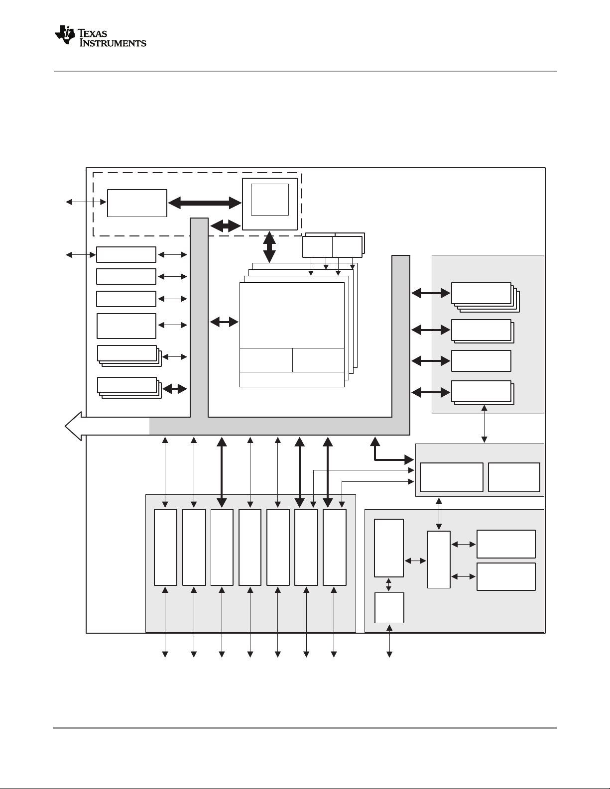
TMS320C6670
Multicore Fixed and Floating-Point System-on-Chip
www.ti.com
The C6670 device has a complete set of development tools that includes: a C compiler, an assembly optimizer to
simplify programming and scheduling, and a Windows® debugger interface for visibility into source code execution.
SPRS689—November 2010
1.3 Functional Block Diagram
Figure 1-1 shows the functional block diagram of the TMS320C6670 device.
Figure 1-1 Functional Block Diagram
Memory Subsystem
64-Bit
DDR3 EMIF
Debug & Trace
Boot ROM
Semaphore
Power
Management
PLL
EDMA
HyperLink
´3
´3
2MB
MSM
SRAM
MSMC
RSA RSA
C66x™
CorePac
32KB L1
P-Cache
1024KB L2 Cache
4 Cores @ 1.0 GHz / 1.2 GHz
TeraNet
32KB L1
D-Cache
´2
C6670
Coprocessors
VCP2
TCP3d
TCP3e
FFTC
Multicore Navigator
´4
´2
´2
ADVANCE INFORMATION
Queue
Manager
6
´
2
IC
Others
Copyright 2010 Texas Instruments Incorporated 13
PCIe 2
UART
SPI
´
AIF2
´
Switch
SRIO 4
Ethernet
2
´
SGMII
Network Coprocessor
Switch
Packet
DMA
Security
Accelerator
Packet
Accelerator
Page 14

TMS320C6670
Multicore Fixed and Floating-Point System-on-Chip
SPRS689—November 2010
2 Device Overview
2.1 Device Characteristics
Table 2-1 provides an overview of the TMS320C6670 DSP. The table shows significant features of the C6670 device,
including the capacity of on-chip RAM, the peripherals, the CPU frequency, and the package type with pin count.
2.2 CPU (DSP Core) Description
Table 2-1 Characteristics of the C6670 Processor (Part 1 of 2)
HARDWARE FEATURES TMS320C6670
ADVANCE INFORMATION
Peripherals
Encoder/Decoder
Coprocessors
Accelerators
On-Chip Memory
C66x CorePac
Revision ID
JTAG BSDL_ID JTAGID register (address location: 0x02620018)
Frequency MHz 1200 (1.2 GHz) [-1200]
Cycle Time ns 0.83 ns [-1200]
Voltage
BGA Package 24 mm × 24 mm 841-Pin Flip-Chip Plastic BGA (CYP)
DDR3 Memory Controller (64-bit bus width) [1.5 V I/O]
(clock source = DDRREFCLKN|P)
EDMA3 (16 independent channels) [CPU/2 clock rate] 1
EDMA3 (64 independent channels) [CPU/3 clock rate] 2
High-speed 1×/2x/4× Serial RapidIO Port (4 lanes) 1
Second generation Antenna Interface (AIF2) 1
2
C 1
I
SPI 1
PCIe (2 lanes) 1
UART 1
10/100/1000 Ethernet MAC (EMAC) 2
Management Data Input/Output (MDIO) 1
64-Bit Timers (Configurable)
(internal clock source = CPU/6 clock frequency)
General-Purpose Input/Output Port (GPIO) 16
VCP2 (clock source = CPU/3 clock frequency) 4
TCP3d (clock source = CPU/2 clock frequency) 2
TCP3e (clock source = CPU/3 clock frequency) 1
FFTC (clock source = CPU/3 clock frequency) 2
Rake/Search Accelerator 4
Packet Accelerator 1
Security Accelerator
Size (Bytes) 6528K
Organization
CorePac Revision ID Register (address location: 0181 2000h) See Section 5.6 ‘‘CorePac Revision’’ on page 88.
Core (V) SmartReflex variable supply
I/O (V) 1.0 V, 1.5 V, and 1.8 V
(1)
www.ti.com
1
Eight 64-bit or Sixteen 32-bit
1
128KB L1 Program Memory Controller
[SRAM/Cache] 128KB L1 Data Memory Controller
[SRAM/Cache] 4096KB L2 Unified Memory/Cache
2048KB MSM SRAM
128KB L3 ROM
See Section 3.3.3 ‘‘JTAG ID (JTAGID) Register
Description’’ on page 65
1000 (1.0 GHz) [-1000]
1 ns [-1000]
14 Device Overview Copyright 2010 Texas Instruments Incorporated
Page 15

TMS320C6670
Multicore Fixed and Floating-Point System-on-Chip
www.ti.com
Table 2-1 Characteristics of the C6670 Processor (Part 2 of 2)
HARDWARE FEATURES TMS320C6670
Process Technology μm 0.040 μm
Product Status
End of Table 2-1
1 The Security Accelerator function is subject to export control and will be enabled only for approved device shipments.
2 ADVA NCE INFOR MATION co ncerns ne w product s in the sa mpling or preproduction phase of development. Characteristic data and other specifications are sub ject to change
without notice.
(2)
Product Preview (PP), Advance Information (AI),
or Production Data (PD)
AI
The C66x Central Processing Unit (CPU) extends the performance of the C64x+ and C674x CPUs through
enhancements and new features. Many of the new features target increased performance for vector processing. The
C64x+ and C674x CPUs support 2-way SIMD operations for 16-bit data and 4-way SIMD operations for 8-bit data.
On the C66x CPU, the vector processing capability is improved by extending the width of the SIMD instructions.
C66x CPUs can execute instructions that operate on 128-bit vectors. For example the QMPY32 instruction is able
to perform the element-to-element multiplication between two vectors of four 32-bit data each. The C66x CPU also
supports SIMD for floating-point operations. Improved vector processing capability (each instruction can process
multiple data in parallel) combined with the natural instruction level parallelism of C6000 architecture (e.g
execution of up to 8 instructions per cycle) results in a very high level of parallelism that can be exploited by DSP
programmers through the use of TI's optimized C/C++ compiler.
SPRS689—November 2010
The C66x CPU consists of eight functional units, two register files, and two data paths as shown in Figure 2-1. The
two general-purpose register files (A and B) each contain 32 32-bit registers for a total of 64 registers. The
general-purpose registers can be used for data or can be data address pointers. The data types supported include
packed 8-bit data, packed 16-bit data, 32-bit data, 40-bit data, and 64-bit data. Multiplies also support 128-bit data.
40-bit-long or 64-bit-long values are stored in register pairs, with the 32 LSBs of data placed in an even register and
the remaining 8 or 32 MSBs in the next upper register (which is always an odd-numbered register). 128-bit data
values are stored in register quadruplets, with the 32 LSBs of data placed in a register that is a multiple of 4 and the
remaining 96 MSBs in the next 3 upper registers.
The eight functional units (.M1, .L1, .D1, .S1, .M2, .L2, .D2, and .S2) are each capable of executing one instruction
every clock cycle. The .M functional units perform all multiply operations. The .S and .L units perform a general set
of arithmetic, logical, and branch functions. The .D units primarily load data from memory to the register file and
store results from the register file into memory.
Each C66x .M unit can perform one of the following fixed-point operations each clock cycle: four 32 × 32 bit
multiplies, sixteen 16 × 16 bit multiplies, four 16 × 32 bit multiplies, four 8 × 8 bit multiplies, four 8 × 8 bit multiplies
with add operations, and four 16 × 16 multiplies with add/subtract capabilities. There is also support for Galois field
multiplication for 8-bit and 32-bit data. Many communications algorithms such as FFTs and modems require
complex multiplication. Each C66x .M unit can perform one 16 × 16 bit complex multiply with or without rounding
capabilities, two 16 × 16 bit complex multiplies with rounding capability, and a 32 × 32 bit complex multiply with
rounding capability. The C66x can also perform two 16 × 16 bit and one 32 × 32 bit complex multiply instructions
that multiply a complex number with a complex conjugate of another number with rounding capability.
Communication signal processing also requires an extensive use of matrix operations. Each C66x .M unit is capable
of multiplying a [1 × 2] complex vector by a [2 × 2] complex matrix per cycle with or without rounding capability.
A version also exists allowing multiplication of the conjugate of a [1 × 2] vector with a [2 × 2] complex matrix.
ADVANCE INFORMATION
Each C66x .M unit also includes IEEE floating-point multiplication operations from the C674x CPU. This includes
one single-precision multiply each cycle and one double precision multiply every 4 cycles. There is also a
mixed-precision multiply that allows multiplication of a single-precision value by a double-precision value and an
operation allowing multiplication of two single-precision numbers resulting in a double-precision number. The
Copyright 2010 Texas Instruments Incorporated Device Overview 15
Page 16

TMS320C6670
Multicore Fixed and Floating-Point System-on-Chip
SPRS689—November 2010
C66x CPU improves the performance over the C674x double-precision multiplies by adding a instruction allowing
one double-precision multiply per cycle and also reduces the number of delay slots from 10 down to 4. Each C66x
.M unit can also perform one the following floating-point operations each clock cycle: one, two, or four
single-precision multiplies or a complex single-precision multiply.
The .L and .S units can now support up to 64-bit operands. This allows for new versions of many of the arithmetic,
logical, and data packing instructions to allow for more parallel operations per cycle. Additional instructions were
added yielding performance enhancements of the floating point addition and subtraction instructions, including the
ability to perform one double precision addition or subtraction per cycle. Conversion to/from integer and
single-precision values can now be done on both .L and .S units on the C66x. Also, by taking advantage of the larger
ADVANCE INFORMATION
operands, instructions were also added to double the number of these conversions that can be done. The .L unit also
has additional instructions for logical AND and OR instructions, as well as, 90 degree or 270 degree rotation of
complex numbers (up to two per cycle). Instructions have also been added that allow for the computing the
conjugate of a complex number.
The MFENCE instruction is a new instruction introduced on the C66x DSP. This instruction will create a CPU stall
until the completion of all the CPU-triggered memory transactions, including:
• Cache line fills
• Writes from L1D to L2 or from the CorePac to MSMC and/or other system endpoints
• Victim write backs
• Block or global coherence operations
•Cache mode changes
• Outstanding XMC prefetch requests
www.ti.com
This is useful as a simple mechanism for programs to wait for these requests to reach their endpoint. It also provides
ordering guarantees for writes arriving at a single endpoint via multiple paths, multiprocessor algorithms that
depend on ordering, and manual coherence operations.
For more details on the C66x CPU and its enhancements over the C64x+ and C674x architectures, see the following
documents ( ‘‘Related Documentation from Texas Instruments’’ on page 59):
• C66x CPU and Instruction Set Reference Guide
• C66x DSP Cache User Guide
• C66x CorePac User Guide
16 Device Overview Copyright 2010 Texas Instruments Incorporated
Page 17
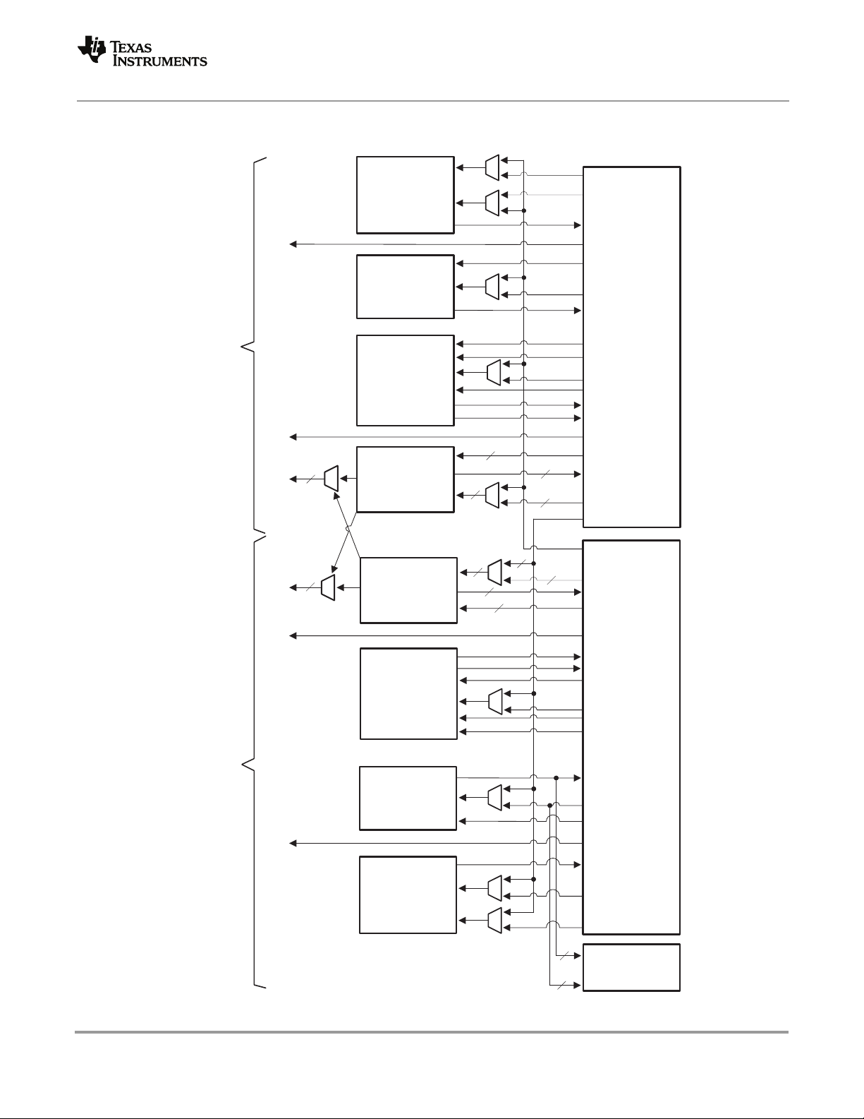
Multicore Fixed and Floating-Point System-on-Chip
www.ti.com
Figure 2-1 shows the DSP core functional units and data paths.
Figure 2-1 TMS320C6670 CPU (DSP Core) Data Paths
TMS320C6670
SPRS689—November 2010
Note:
Default bus width
is 64 bits
(i.e. a register pair)
Data Path A
ST1
LD1
DA1
DA2
LD2
src1
.L1
src2
dst
Register
File A
(A0, A1, A2,
...A31)
src1
.S1
.M1
32
32
.D1
.D2
.M2
src2
dst
src1
src1_hi
src2
src2_hi
dst2
dst1
src1
dst
src2
src2
src1
dst1
dst2
src2_hi
src2
src1_hi
src1
dst
32
32
32
32
32
32
32
2
´
1
´
32
32
Register
File B
(B0, B1, B2,
...B31)
ADVANCE INFORMATION
Data Path B
dst
.S2
ST2
.L2
66xx
Copyright 2010 Texas Instruments Incorporated Device Overview 17
src2
src1
dst
src2
src1
32
Control
Register
32
Page 18
TMS320C6670
Multicore Fixed and Floating-Point System-on-Chip
SPRS689—November 2010
2.3 Memory Map Summary
Table 2-2 shows the memory map address ranges of the TMS320C6670 device.
Table 2-2 TMS320C6670 Memory Map Summary (Part 1 of 9)
Logical 32 bit Address Physical 36 bit Address
0000 0000 007F FFFF 0 0000 0000 0 007F FFFF 8M Reserved
0080 0000 008F FFFF 0 0080 0000 0 008F FFFF 1M L2 SRAM
0090 0000 00DF FFFF 0 0090 0000 0 00DF FFFF 5M Reserved
ADVANCE INFORMATION
00E00000 00E0 7FFF 0 00E00000 0 00E0 7FFF 32K L1P SRAM
00E08000 00EF FFFF 0 00E08000 0 00EF FFFF 1M-32K Reserved
00F00000 00F0 7FFF 0 00F00000 0 00F0 7FFF 32K L1D SRAM
00F08000 00FF FFFF 0 00F08000 0 00FF FFFF 1M-32K Reserved
0100 0000 01BF FFFF 0 0100 0000 0 01BF FFFF 12 M C66x CorePac Registers
01C0 0000 01CF FFFF 0 01C0 0000 0 01CF FFFF 1M Reserved
01D0 0000 01D0 007F 0 01D0 0000 0 01D0 007F 128 Tracer 0
01D0 0080 01D0 7FFF 0 01D0 0080 0 01D0 7FFF 32K-128 Reserved
01D0 8000 01D0 807F 0 01D0 8000 0 01D0 807F 128 Tracer 1
01D0 8080 01D0 FFFF 0 01D0 8080 0 01D0 FFFF 32K-128 Reserved
01D1 0000 01D1 007F 0 01D1 0000 0 01D1 007F 128 Tracer 2
01D1 0080 01D1 7FFF 0 01D1 0080 0 01D1 7FFF 32K-128 Reserved
01D1 8000 01D1 807F 0 01D1 8000 0 01D1 807F 128 Tracer 3
01D1 8080 01D1 FFFF 0 01D1 8080 0 01D1 FFFF 32K-128 Reserved
01D2 0000 01D2 007F 0 01D2 0000 0 01D2 007F 128 Tracer 4
01D2 0080 01D2 7FFF 0 01D2 0080 0 01D2 7FFF 32K-128 Reserved
01D2 8000 01D2 807F 0 01D2 8000 0 01D2 807F 128 Tracer 5
01D2 8080 01D2 FFFF 0 01D2 8080 0 01D2 FFFF 32K-128 Reserved
01D3 0000 01D3 007F 0 01D3 0000 0 01D3 007F 128 Tracer 6
01D3 0080 01D3 7FFF 0 01D3 0080 0 01D3 7FFF 32K-128 Reserved
01D3 8000 01D3 807F 0 01D3 8000 0 01D3 807F 128 Tracer 7
01D3 8080 01D3 FFFF 0 01D3 8080 0 01D3 FFFF 32K-128 Reserved
01D4 0000 01D4 007F 0 01D4 0000 0 01D4 007F 128 Tracer 8
01D4 0080 01D4 7FFF 0 01D4 0080 0 01D4 7FFF 32K-128 Reserved
01D4 8000 01D4 807F 0 01D4 8000 0 01D4 807F 128 Tracer 9
01D4 8080 01D4 FFFF 0 01D4 8080 0 01D4 FFFF 32K-128 Reserved
01D5 0000 01D5 007F 0 01D5 0000 0 01D5 007F 128 Tracer 10
01D5 0080 01D5 7FFF 0 01D5 0080 0 01D5 7FFF 32K-128 Reserved
01D5 8000 01D5 807F 0 01D5 8000 0 01D5 807F 128 Tracer 11
01D5 8080 01D5 FFFF 0 01D5 8080 0 01D5 FFFF 32K-128 Reserved
01D6 0000 01D6 007F 0 01D6 0000 0 01D6 007F 128 Tracer 12
01D6 0080 01D6 7FFF 0 01D6 0080 0 01D6 7FFF 32K-128 Reserved
01D6 8000 01D6 807F 0 01D6 8000 0 01D6 807F 128 Tracer 13
01D6 8080 01D6 FFFF 0 01D6 8080 0 01D6 FFFF 32K-128 Reserved
01D7 0000 01D7 007F 0 01D7 0000 0 01D7 007F 128 Tracer 14
01D7 0080 01D7 7FFF 0 01D7 0080 0 01D7 7FFF 32K-128 Reserved
01D7 8000 01D7 807F 0 01D7 8000 0 01D7 807F 128 Tracer 15
www.ti.com
Bytes DescriptionStart End Start End
18 Device Overview Copyright 2010 Texas Instruments Incorporated
Page 19

Multicore Fixed and Floating-Point System-on-Chip
www.ti.com
Table 2-2 TMS320C6670 Memory Map Summary (Part 2 of 9)
Logical 32 bit Address Physical 36 bit Address
Bytes DescriptionStart End Start End
01D7 8080 01D7 FFFF 0 01D7 8080 0 01D7 FFFF 32K-128 Reserved
01D8 0000 01D8 007F 0 01D8 0000 0 01D8 007F 128 Reserved
01D8 0080 01D8 7FFF 0 01D8 0080 0 01D8 7FFF 32K-128 Reserved
01D8 8000 01DF FFFF 0 01D8 8000 0 01DF FFFF 480K Reserved
01E0 0000 01E3 FFFF 0 01E0 0000 0 01E3 FFFF 256K Reserved
01E4 0000 01E7 FFFF 0 01E4 0000 0 01E7 FFFF 256K Reserved
01E8 0000 01EB FFFF 0 01E8 0000 0 01EB FFFF 256K Reserved
01EC 0000 01EF FFFF 0 01EC 0000 0 01EF FFFF 256K Reserved
01F0 0000 01F7 FFFF 0 01F0 0000 0 01F7 FFFF 512k AIF2 Control
01F80000 01F8FFFF 01F80000 01F8FFFF 64K Reserved
01F90000 01F9FFFF 01F90000 01F9FFFF 64K Reserved
01FA0000 01FBFFFF 01FA0000 01FBFFFF 128K Reserved
01FC0000 01FDFFFF 01FC0000 01FDFFFF 128K Reserved
01FE 0000 01FF FFFF 0 01FE 0000 0 01FF FFFF 128k Reserved
0200 0000 0208 FFFF 0 0200 0000 0 0208 FFFF 576K Packet Accelerator Configuration
0209 0000 020B FFFF 0 0209 0000 0 020B FFFF 192K Ethernet Switch Subsystem Configuration
020C 0000 020F FFFF 0 020C 0000 0 020F FFFF 256K Security Accelerator Subsystem Configuration
02100000 0210FFFF 02100000 0210FFFF 64K Reserved
02110000 0211FFFF 02110000 0211FFFF 64K Reserved
02120000 0213FFFF 02120000 0213FFFF 128K Reserved
02140000 0215FFFF 02140000 0215FFFF 128K Reserved
0216 0000 0217 FFFF 0 0216 0000 0 0217 FFFF 128K Reserved
02180000 02187FFF 02180000 02187FFF 32k Reserved
02188000 0218FFFF 02188000 0218FFFF 32k Reserved
02190000 0219FFFF 02190000 0219FFFF 64k Reserved
021A0000 021AFFFF 021A0000 021AFFFF 64K Reserved
021B 0000 021B FFFF 0 021B 0000 0 021B FFFF 64K Reserved
021C 0000 021C 03FF 0 021C 0000 0 021C 03FF 1K TCP3d-A
021C 0400 021C 7FFF 0 021C 0400 0 021C 7FFF 31K Reserved
021C 8000 021C 83FF 0 021C 8000 0 021C 83FF 1K TCP3d-B
021C 8400 021C FFFF 0 021C 8400 0 021C FFFF 31K Reserved
021D 0000 021D 00FF 0 021D 0000 0 021D 00FF 256 VCP2_A
021D 0100 021D 3FFF 0 021D 0100 0 021D 3FFF 16K Reserved
021D 4000 021D 40FF 0 021D 4000 0 021D 40FF 256 VCP2_B
021D 4100 021D 7FFF 0 021D 4100 0 021D 7FFF 16K Reserved
021D 8000 021D 80FF 0 021D 8000 0 021D 80FF 256 VCP2_C
021D 8100 021D BFFF 0 021D 8100 0 021D BFFF 16K Reserved
021D C000 021D C0FF 0 021D C000 0 021D C0FF 256 VCP2_D
021D C100 021D FFFF 0 021D C100 0 021D FFFF 16K Reserved
021E 0000 021E 0FFF 0 021E 0000 0 021E 0FFF 4K TCP3e
021E 1000 021E FFFF 0 021E 1000 0 021E FFFF 60k Reserved
021F 0000 021F 07FF 0 021F 0000 0 021F 07FF 2K FFTC-A Configuration
021F 0800 021F 3FFF 0 021F 0800 0 021F 3FFF 14K Reserved
SPRS689—November 2010
TMS320C6670
ADVANCE INFORMATION
Copyright 2010 Texas Instruments Incorporated Device Overview 19
Page 20

TMS320C6670
Multicore Fixed and Floating-Point System-on-Chip
SPRS689—November 2010
Table 2-2 TMS320C6670 Memory Map Summary (Part 3 of 9)
Logical 32 bit Address Physical 36 bit Address
021F 4000 021F 47FF 0 021F 4000 0 021F 47FF 2K FFTC-B Configuration
021F 4800 021F FFFF 0 021F 4800 0 021F FFFF 46K Reserved
0220 0000 0220 007F 0 0220 0000 0 0220 007F 128 Timer0
0220 0080 0220 FFFF 0 0220 0080 0 0220 FFFF 64K-128 Reserved
0221 0000 0221 007F 0 0221 0000 0 0221 007F 128 Timer1
0221 0080 0221 FFFF 0 0221 0080 0 0221 FFFF 64K-128 Reserved
ADVANCE INFORMATION
0222 0000 0222 007F 0 0222 0000 0 0222 007F 128 Timer2
0222 0080 0222 FFFF 0 0222 0080 0 0222 FFFF 64K-128 Reserved
0223 0000 0223 007F 0 0223 0000 0 0223 007F 128 Timer3
0223 0080 0223 FFFF 0 0223 0080 0 0223 FFFF 64K-128 Reserved
0224 0000 0224 007F 0 0224 0000 0 0224 007F 128 Timer4
0224 0080 0224 FFFF 0 0224 0080 0 0224 FFFF 64K-128 Reserved
0225 0000 0225 007F 0 0225 0000 0 0225 007F 128 Timer5
0225 0080 0225 FFFF 0 0225 0080 0 0225 FFFF 64K-128 Reserved
0226 0000 0226 007F 0 0226 0000 0 0226 007F 128 Timer6
0226 0080 0226 FFFF 0 0226 0080 0 0226 FFFF 64K-128 Reserved
0227 0000 0227 007F 0 0227 0000 0 0227 007F 128 Timer7
0227 0080 0227 FFFF 0 0227 0080 0 0227 FFFF 64K-128 Reserved
0228 0000 0228 007F 0 0228 0000 0 0228 007F 128 Reserved
0228 0080 0228 FFFF 0 0228 0080 0 0228 FFFF 64K-128 Reserved
0229 0000 0229 007F 0 0229 0000 0 0229 007F 128 Reserved
0229 0080 0229 FFFF 0 0229 0080 0 0229 FFFF 64K-128 Reserved
022A 0000 022A 007F 0 022A 0000 0 022A 007F 128 Reserved
022A 0080 022A FFFF 0 022A 0080 0 022A FFFF 64K-128 Reserved
022B 0000 022B 007F 0 022B 0000 0 022B 007F 128 Reserved
022B 0080 022B FFFF 0 022B 0080 0 022B FFFF 64K-128 Reserved
022C 0000 022C 007F 0 022C 0000 0 022C 007F 128 Reserved
022C 0080 022C FFFF 0 022C 0080 0 022C FFFF 64K-128 Reserved
022D 0000 022D 007F 0 022D 0000 0 022D 007F 128 Reserved
022D 0080 022D FFFF 0 022D 0080 0 022D FFFF 64K-128 Reserved
022E 0000 022E 007F 0 022E 0000 0 022E 007F 128 Reserved
022E 0080 022E FFFF 0 022E 0080 0 022E FFFF 64K-128 Reserved
022F 0000 022F 007F 0 022F 0000 0 022F 007F 128 Reserved
022F 0080 022F FFFF 0 022F 0080 0 022F FFFF 64K-128 Reserved
0230 0000 0230 FFFF 0 0230 0000 0 0230 FFFF 64K Reserved
0231 0000 0231 01FF 0 0231 0000 0 0231 01FF 512 PLL Controller
0231 0200 0231 FFFF 0 0231 0200 0 0231 FFFF 64K-512 Reserved
0232 0000 0232 00FF 0 0232 0000 0 0232 00FF 256 GPIO
0232 0100 0232 FFFF 0 0232 0100 0 0232 FFFF 64K-256 Reserved
0233 0000 0233 03FF 0 0233 0000 0 0233 03FF 1K SmartReflex
0233 0400 0233 FFFF 0 0233 0400 0 0233 FFFF 63K Reserved
0234 0000 0234 FFFF 0 0234 0000 0 0234 FFFF 64K Reserved
0235 0000 0235 0FFF 0 0235 0000 0 0235 0FFF 4K Power Sleep Controller
www.ti.com
Bytes DescriptionStart End Start End
20 Device Overview Copyright 2010 Texas Instruments Incorporated
Page 21

Multicore Fixed and Floating-Point System-on-Chip
www.ti.com
Table 2-2 TMS320C6670 Memory Map Summary (Part 4 of 9)
Logical 32 bit Address Physical 36 bit Address
Bytes DescriptionStart End Start End
0235 1000 0235 FFFF 0 0235 1000 0 0235 FFFF 64K-4K Reserved
0236 0000 0236 03FF 0 0236 0000 0 0236 03FF 1K Memory Protection Unit (MPU) 0
0236 0400 0236 7FFF 0 0236 0400 0 0236 7FFF 31K Reserved
0236 8000 0236 83FF 0 0236 8000 0 0236 83FF 1K Memory Protection Unit (MPU) 1
0236 8400 0236 FFFF 0 0236 8400 0 0236 FFFF 31K Reserved
0237 0000 0237 03FF 0 0237 0000 0 0237 03FF 1K Memory Protection Unit (MPU) 2
0237 0400 0237 7FFF 0 0237 0400 0 0237 7FFF 31K Reserved
0237 8000 0237 83FF 0 0237 8000 0 0237 83FF 1K Memory Protection Unit (MPU) 3
0237 8400 0237 FFFF 0 0237 8400 0 0237 FFFF 31K Reserved
0238 0000 0238 03FF 0 0238 0000 0 0238 03FF 1K Reserved
0238 0400 023F FFFF 0 0238 0400 0 023F FFFF 511K Reserved
0240 0000 0243 FFFF 0 0240 0000 0 0243 FFFF 256K Reserved
0244 0000 0244 3FFF 0 0244 0000 0 0244 3FFF 16K DSP Trace Formatter 0
0244 4000 0244 FFFF 0 0244 4000 0 0244 FFFF 48K Reserved
0245 0000 0245 3FFF 0 0245 0000 0 0245 3FFF 16K DSP Trace Formatter 1
0245 4000 0245 FFFF 0 0245 4000 0 0245 FFFF 48K Reserved
0246 0000 0246 3FFF 0 0246 0000 0 0246 3FFF 16K DSP Trace Formatter 2
0246 4000 0246 FFFF 0 0246 4000 0 0246 FFFF 48K Reserved
0247 0000 0247 3FFF 0 0247 0000 0 0247 3FFF 16K DSP Trace Formatter 3
0247 4000 0247 FFFF 0 0247 4000 0 0247 FFFF 48K Reserved
0248 0000 0248 3FFF 0 0248 0000 0 0248 3FFF 16K Reserved
0248 4000 0248 FFFF 0 0248 4000 0 0248 FFFF 48K Reserved
0249 0000 0249 3FFF 0 0249 0000 0 0249 3FFF 16K Reserved
0249 4000 0249 FFFF 0 0249 4000 0 0249 FFFF 48K Reserved
024A 0000 024A 3FFF 0 024A 0000 0 024A 3FFF 16K Reserved
024A 4000 024A FFFF 0 024A 4000 0 024A FFFF 48K Reserved
024B 0000 024B 3FFF 0 024B 0000 0 024B 3FFF 16K Reserved
024B 4000 024B FFFF 0 024B 4000 0 024B FFFF 48K Reserved
024C 0000 024C 01FF 0 024C 0000 0 024C 01FF 512 Reserved
024C 0200 024C 03FF 0 024C 0200 0 024C 03FF 1K-512 Reserved
024C 0400 024C 07FF 0 024C 0400 0 024C 07FF 1K Reserved
024C 0800 024C FFFF 0 024C 0800 0 024C FFFF 62K Reserved
024D 0000 024F FFFF 0 024D 0000 0 024F FFFF 192K Reserved
0250 0000 0250 007F 0 0250 0000 0 0250 007F 128 Reserved
0250 0080 0250 7FFF 0 0250 0080 0 0250 7FFF 32K-128 Reserved
0250 8000 0250 FFFF 0 0250 8000 0 0250 FFFF 32K Reserved
0251 0000 0251 FFFF 0 0251 0000 0 0251 FFFF 64K Reserved
0252 0000 0252 03FF 0 0252 0000 0 0252 03FF 1K Reserved
0252 0400 0252 FFFF 0 0252 0400 0 0252 FFFF 64K-1K Reserved
0253 0000 0253 007F 0 0253 0000 0 0253 007F 128 I2C Data & Control
0253 0080 0253 FFFF 0 0253 0080 0 0253 FFFF 64K-128 Reserved
0254 0000 0254 003F 0 0254 0000 0 0254 003F 64 UART
02540 400 0254 FFFF 0 02540 400 0 0254 FFFF 64K-64 Reserved
TMS320C6670
SPRS689—November 2010
ADVANCE INFORMATION
Copyright 2010 Texas Instruments Incorporated Device Overview 21
Page 22

TMS320C6670
Multicore Fixed and Floating-Point System-on-Chip
SPRS689—November 2010
Table 2-2 TMS320C6670 Memory Map Summary (Part 5 of 9)
Logical 32 bit Address Physical 36 bit Address
0255 0000 0257 FFFF 0 0255 0000 0 0257 FFFF 192K Reserved
0258 0000 025B FFFF 0 0258 0000 0 025B FFFF 256K Reserved
025C 0000 025F FFFF 0 025C 0000 0 025F FFFF 256K Reserved
0260 0000 0260 1FFF 0 0260 0000 0 0260 1FFF 8K Secondary Interrupt Contoller (INTC) 0
0260 2000 0260 3FFF 0 0260 2000 0 0260 3FFF 8K Reserved
0260 4000 0260 5FFF 0 0260 4000 0 0260 5FFF 8K Secondary Interrupt Contoller (INTC) 1
ADVANCE INFORMATION
0260 6000 0260 7FFF 0 0260 6000 0 0260 7FFF 8K Reserved
0260 8000 0260 9FFF 0 0260 8000 0 0260 9FFF 8K Secondary Interrupt Contoller (INTC) 2
0260 A000 0260 BFFF 0 0260 A000 0 0260 BFFF 8K Reserved
0260 C000 0260 DFFF 0 0260 C000 0 0260 DFFF 8K Reserved
0260 E000 0260 FFFF 0 0260 E000 0 0260 FFFF 8K Reserved
0261 0000 0261 FFFF 0 0261 0000 0 0261 FFFF 64K Reserved
0262 0000 0262 03FF 0 0262 0000 0 0262 03FF 1K Chip-Level Registers
0262 0400 0262 FFFF 0 0262 0400 0 0262 FFFF 63K Reserved
0263 0000 0263 FFFF 0 0263 0000 0 0263 FFFF 64K Reserved
0264 0000 0264 07FF 0 0264 0000 0 0264 07FF 2K Semaphore
0264 0800 0264 FFFF 0 0264 0800 0 0264 FFFF 64K-2K Reserved
0265 0000 026F FFFF 0 0265 0000 0 026F FFFF 704K Reserved
0270 0000 0270 7FFF 0 0270 0000 0 0270 7FFF 32K EDMA Channel Controller (TPCC) 0
0270 8000 0271 FFFF 0 0270 8000 0 0271 FFFF 96K Reserved
0272 0000 0272 7FFF 0 0272 0000 0 0272 7FFF 32K EDMA Channel Controller (TPCC) 1
0272 8000 0273 FFFF 0 0272 8000 0 0273 FFFF 96K Reserved
02740000 0274 7FFF 0 02740000 0 0274 7FFF 32K EDMA Channel Controller (TPCC) 2
0274 8000 0275 FFFF 0 0274 8000 0 0275 FFFF 96K Reserved
0276 0000 0276 03FF 0 0276 0000 0 0276 03FF 1K EDMA TPCC0 Transfer Controller (TPTC) 0
0276 0400 0276 7FFF 0 0276 0400 0 0276 7FFF 31K Reserved
0276 8000 0276 83FF 0 0276 8000 0 0276 83FF 1K EDMA TPCC0 Transfer Controller (TPTC) 1
0276 8400 0276 FFFF 0 0276 8400 0 0276 FFFF 31K Reserved
0277 0000 0277 03FF 0 0277 0000 0 0277 03FF 1K EDMA TPCC1 Transfer Controller (TPTC) 0
0277 0400 0277 7FFF 0 0277 0400 0 0277 7FFF 31K Reserved
0277 8000 0277 83FF 0 0277 8000 0 0277 83FF 1K EDMA TPCC1 Transfer Controller (TPTC) 1
0278 0400 0277 FFFF 0 0278 0400 0 0277 FFFF 31K Reserved
0278 0000 0278 03FF 0 0278 0000 0 0278 03FF 1K EDMA TPCC1 Transfer Controller (TPTC) 2
0278 0400 0278 7FFF 0 0278 0400 0 0278 7FFF 31K Reserved
0278 8000 0278 83FF 0 0278 8000 0 0278 83FF 1K EDMA TPCC1 Transfer Controller (TPTC) 3
0278 8400 0278 FFFF 0 0278 8400 0 0278 FFFF 31K Reserved
0279 0000 0279 03FF 0 0279 0000 0 0279 03FF 1K EDMA TPCC2 Transfer Controller (TPTC) 0
0279 0400 0279 7FFF 0 0279 0400 0 0279 7FFF 31K Reserved
0279 8000 0279 83FF 0 0279 8000 0 0279 83FF 1K EDMA TPCC2 Transfer Controller (TPTC) 1
0279 8400 0279 FFFF 0 0279 8400 0 0279 FFFF 31K Reserved
027A 0000 027A 03FF 0 027A 0000 0 027A 03FF 1K EDMA TPCC2 Transfer Controller (TPTC) 2
027A 0400 027A 7FFF 0 027A 0400 0 027A 7FFF 31K Reserved
027A 8000 027A 83FF 0 027A 8000 0 027A 83FF 1K EDMA TPCC2 Transfer Controller (TPTC) 3
www.ti.com
Bytes DescriptionStart End Start End
22 Device Overview Copyright 2010 Texas Instruments Incorporated
Page 23

TMS320C6670
Multicore Fixed and Floating-Point System-on-Chip
www.ti.com
Table 2-2 TMS320C6670 Memory Map Summary (Part 6 of 9)
Logical 32 bit Address Physical 36 bit Address
Bytes DescriptionStart End Start End
027A 8400 027A FFFF 0 027A 8400 0 027A FFFF 31K Reserved
027B 0000 027B FFFF 0 027B 0000 0 027B FFFF 64K Reserved
027C 0000 027C FFFF 0 027C 0000 0 027C FFFF 64k Reserved
027D 0000 027D 3FFF 0 027D 0000 0 027D 3FFF 16k TI Embedded Trace Buffer (TETB) - Core 0
027D 4000 027D FFFF 0 027D 4000 0 027D FFFF 48k Reserved
027E 0000 027E 3FFF 0 027E 0000 0 027E 3FFF 16k TI Embedded Trace Buffer (TETB) - Core 1
027E 4000 027E FFFF 0 027E 4000 0 027E FFFF 48k Reserved
027F 0000 027F 3FFF 0 027F 0000 0 027F 3FFF 16k TI Embedded Trace Buffer (TETB) - Core 2
027F 4000 027F FFFF 0 027F 4000 0 027F FFFF 48k Reserved
0280 0000 0280 3FFF 0 0280 0000 0 0280 3FFF 16k TI Embedded Trace Buffer (TETB) - Core 3
0280 4000 0280 FFFF 0 0280 4000 0 0280 FFFF 48k Reserved
0281 0000 0281 3FFF 0 0281 0000 0 0281 3FFF 16k Reserved
0281 4000 0281 FFFF 0 0281 4000 0 0281 FFFF 48k Reserved
0282 0000 0282 3FFF 0 0282 0000 0 0282 3FFF 16k Reserved
0282 4000 0282 FFFF 0 0282 4000 0 0282 FFFF 48k Reserved
0283 0000 0283 3FFF 0 0283 0000 0 0283 3FFF 16k Reserved
0283 4000 0283 FFFF 0 0283 4000 0 0283 FFFF 48k Reserved
0284 0000 0284 3FFF 0 0284 0000 0 0284 3FFF 16k Reserved
0284 4000 0284 FFFF 0 0284 4000 0 0284 FFFF 48k Reserved
0285 0000 0285 7FFF 0 0285 0000 0 0285 7FFF 32k TI Embedded Trace Buffer (TETB) - System
0285 8000 0285 FFFF 0 0285 8000 0 0285 FFFF 32k Reserved
0286 0000 028F FFFF 0 0286 0000 0 028F FFFF 640K Reserved
0290 0000 0290 7FFF 0 0290 0000 0 0290 7FFF 32K Serial RapidIO Configuration
0290 8000 029F FFFF 0 0290 8000 0 029F FFFF 1M-32k Reserved
02A0 0000 02AF FFFF 0 02A0 0000 0 02AF FFFF 1M Queue Manager Subsystem Configuration
02B0 0000 02BF FFFF 0 02B0 0000 0 02BF FFFF 1M Reserved
02C0 0000 02FF FFFF 0 02C0 0000 0 02FF FFFF 4M Reserved
03000 000 07FF FFFF 0 03000 000 0 07FF FFFF 80M Reserved
0800 0000 0800 FFFF 0 0800 0000 0 0800 FFFF 64k Extended Memory Controller (XMC) Configuration
0801 0000 0BBF FFFF 0 0801 0000 0 0BBF FFFF 60M-64k Reserved
0BC0 0000 0BCF FFFF 0 0BC0 0000 0 0BCF FFFF 1M Multicore Shared Memory Controller (MSMC) Config
0BD0 0000 0BFF FFFF 0 0BD0 0000 0 0BFF FFFF 3M Reserved
0C00 0000 0C1F FFFF 0 0C00 0000 0 0C1F FFFF 2M Multicore Shared Memory (MSM)
0C20 0000 0C3F FFFF 0 0C20 0000 0 0C3F FFFF 2M Reserved
0C40 0000 0FFF FFFF 0 0C40 0000 0 0FFF FFFF 60 M Reserved
1000 0000 107F FFFF 0 1000 0000 0 107F FFFF 8M Reserved
1080 0000 108F FFFF 0 1080 0000 0 108F FFFF 1M Core 0 L2 SRAM
1090 0000 10DF FFFF 0 1090 0000 0 10DF FFFF 5M Reserved
10E0 0000 10E0 7FFF 0 10E0 0000 0 10E0 7FFF 32k Core 0 L1P SRAM
10E0 8000 10EF FFFF 0 10E0 8000 0 10EF FFFF 1M-32K Reserved
10F0 0000 10F0 7FFF 0 10F0 0000 0 10F0 7FFF 32k Core 0 L1D SRAM
10F0 8000 117F FFFF 0 10F0 8000 0 117F FFFF 9M-32k Reserved
1180 0000 118F FFFF 0 1180 0000 0 118F FFFF 1M Core 1 L2 SRAM
SPRS689—November 2010
ADVANCE INFORMATION
Copyright 2010 Texas Instruments Incorporated Device Overview 23
Page 24

TMS320C6670
Multicore Fixed and Floating-Point System-on-Chip
SPRS689—November 2010
Table 2-2 TMS320C6670 Memory Map Summary (Part 7 of 9)
Logical 32 bit Address Physical 36 bit Address
1190 0000 11DF FFFF 0 1190 0000 0 11DF FFFF 5M Reserved
11E0 0000 11E0 7FFF 0 11E0 0000 0 11E0 7FFF 32k Core 1 L1P SRAM
11E0 8000 11EF FFFF 0 11E0 8000 0 11EF FFFF 1M-32K Reserved
11F0 0000 11F0 7FFF 0 11F0 0000 0 11F0 7FFF 32k Core 1 L1D SRAM
11F0 8000 127F FFFF 0 11F0 8000 0 127F FFFF 9M-32k Reserved
1280 0000 128F FFFF 0 1280 0000 0 128F FFFF 1M Core 2 L2 SRAM
ADVANCE INFORMATION
1290 0000 12DF FFFF 0 1290 0000 0 12DF FFFF 5M Reserved
12E0 0000 12E0 7FFF 0 12E0 0000 0 12E0 7FFF 32k Core 2 L1P SRAM
12E0 8000 12EF FFFF 0 12E0 8000 0 12EF FFFF 1M-32K Reserved
12F0 0000 12F0 7FFF 0 12F0 0000 0 12F0 7FFF 32k Core 2 L1D SRAM
12F0 8000 137F FFFF 0 12F0 8000 0 137F FFFF 9M-32k Reserved
1380 0000 1388 FFFF 0 1380 0000 0 1388 FFFF 1M Core 3 L2 SRAM
1390 0000 13DF FFFF 0 1390 0000 0 13DF FFFF 5M Reserved
13E0 0000 13E0 7FFF 0 13E0 0000 0 13E0 7FFF 32k Core 3 L1P SRAM
13E0 8000 13EF FFFF 0 13E0 8000 0 13EF FFFF 1M-32K Reserved
13F0 0000 13F0 7FFF 0 13F0 0000 0 13F0 7FFF 32k Core 3 L1D SRAM
13F0 8000 147F FFFF 0 13F0 8000 0 147F FFFF 9M-32k Reserved
1480 0000 1487 FFFF 0 1480 0000 0 1487 FFFF 512K Reserved
1488 0000 148F FFFF 0 1488 0000 0 148F FFFF 512K Reserved
1490 0000 14DF FFFF 0 1490 0000 0 14DF FFFF 5M Reserved
14E0 0000 14E0 7FFF 0 14E0 0000 0 14E0 7FFF 32k Reserved
14E0 8000 14EF FFFF 0 14E0 8000 0 14EF FFFF 1M-32K Reserved
14F0 0000 14F0 7FFF 0 14F0 0000 0 14F0 7FFF 32k Reserved
14F0 8000 157F FFFF 0 14F0 8000 0 157F FFFF 9M-32k Reserved
1580 0000 1587 FFFF 0 1580 0000 0 1587 FFFF 512K Reserved
1588 0000 158F FFFF 0 1588 0000 0 158F FFFF 512K Reserved
1590 0000 15DF FFFF 0 1590 0000 0 15DF FFFF 5M Reserved
15E0 0000 15E0 7FFF 0 15E0 0000 0 15E0 7FFF 32k Reserved
15E0 8000 15EF FFFF 0 15E0 8000 0 15EF FFFF 1M-32K Reserved
15F0 0000 15F0 7FFF 0 15F0 0000 0 15F0 7FFF 32k Reserved
15F0 8000 167F FFFF 0 15F0 8000 0 167F FFFF 9M-32k Reserved
1680 0000 1687 FFFF 0 1680 0000 0 1687 FFFF 512K Reserved
1688 0000 168F FFFF 0 1688 0000 0 168F FFFF 512K Reserved
1690 0000 16DF FFFF 0 1690 0000 0 16DF FFFF 5M Reserved
16E0 0000 16E0 7FFF 0 16E0 0000 0 16E0 7FFF 32k Reserved
16E0 8000 16EF FFFF 0 16E0 8000 0 16EF FFFF 1M-32K Reserved
16F0 0000 16F0 7FFF 0 16F0 0000 0 16F0 7FFF 32k Reserved
16F0 8000 177F FFFF 0 16F0 8000 0 177F FFFF 9M-32k Reserved
1780 0000 1787 FFFF 0 1780 0000 0 1787 FFFF 512K Reserved
1788 0000 178F FFFF 0 1788 0000 0 178F FFFF 512K Reserved
1790 0000 17DF FFFF 0 1790 0000 0 17DF FFFF 5M Reserved
17E0 0000 17E0 7FFF 0 17E0 0000 0 17E0 7FFF 32k Reserved
17E0 8000 17EF FFFF 0 17E0 8000 0 17EF FFFF 1M-32K Reserved
www.ti.com
Bytes DescriptionStart End Start End
24 Device Overview Copyright 2010 Texas Instruments Incorporated
Page 25

Multicore Fixed and Floating-Point System-on-Chip
www.ti.com
Table 2-2 TMS320C6670 Memory Map Summary (Part 8 of 9)
Logical 32 bit Address Physical 36 bit Address
Bytes DescriptionStart End Start End
17F0 0000 17F0 7FFF 0 17F0 0000 0 17F0 7FFF 32k Reserved
17F0 8000 1FFF FFFF 0 17F0 8000 0 1FFF FFFF 129M-32k Reserved
2000 0000 200F FFFF 0 2000 0000 0 200F FFFF 1M System Trace Manager (STM) Configuration
2010 0000 201F FFFF 0 2010 0000 0 201F FFFF 1M Reserved
20200000 205FFFFF 20200000 205FFFFF 4M Reserved
2060 0000 206F FFFF 0 2060 0000 0 206F FFFF 1M TCP3d-B Data
2070 0000 207F FFFF 0 2070 0000 0 207F FFFF 1M Reserved
2080 0000 208F FFFF 0 2080 0000 0 208F FFFF 1M TCP3d-A Data
2090 0000 2090 1FFF 0 2090 0000 0 2090 1FFF 8K TCP3e Data Write Port
2090 2000 2090 3FFF 0 2090 2000 0 2090 3FFF 8K TCP3e Data Read Port
2090 4000 209F FFFF 0 2090 4000 0 209F FFFF 1M-16K Reserved
20A0 0000 20A3 FFFF 0 20A0 0000 0 20A3 FFFF 256K Reserved
20A4 0000 20A4 FFFF 0 20A4 0000 0 20A4 FFFF 64K Reserved
20A5 0000 20AF FFFF 0 20A5 0000 0 20AF FFFF 704k Reserved
20B0 0000 20B1 FFFF 0 20B0 0000 0 20B1 FFFF 128k Boot ROM
20B2 0000 20BE FFFF 0 20B2 0000 0 20BE FFFF 832k Reserved
20BF 0000 20BF 03FF 0 20BF 0000 0 20BF 03FF 1k SPI
20BF 0400 20BF FFFF 0 20BF 0400 0 20BF FFFF 63k Reserved
20C0 0000 20C0 00FF 0 20C0 0000 0 20C0 00FF 256 Reserved
20C0 0100 20FF FFFF 0 20C0 0100 0 20FF FFFF 4M-256 Reserved
2100 0000 2100 00FF 0 2100 0000 0 2100 00FF 256 DDR3 EMIF Configuration
2100 0100 213F FFFF 0 2100 0100 0 213F FFFF 4M-256 Reserved
2140 0000 2140 03FF 0 2140 0000 0 2140 03FF 1K HyperLink Config
2140 0400 217F FFFF 0 2140 0400 0 217F FFFF 4M-1K Reserved
2180 0000 2180 7FFF 0 2180 0000 0 2180 7FFF 32K PCIe Config
2180 8000 21BF FFFF 0 2180 8000 0 21BF FFFF 4M-32K Reserved
21C0 0000 21FF FFFF 0 21C0 0000 0 21FF FFFF 4M Reserved
2200 0000 229F FFFF 0 2200 0000 0 229F FFFF 10M Reserved
22A0 0000 22A0 FFFF 0 22A0 0000 0 22A0 FFFF 64K VCP2_A
22A1 0000 22AF FFFF 0 22A1 0000 0 22AF FFFF 1M-64K Reserved
22B0 0000 22B0 FFFF 0 22B0 0000 0 22B0 FFFF 64K VCP2_B
22B1 0000 22BF FFFF 0 22B1 0000 0 22BF FFFF 1M-64K Reserved
22C0 0000 22C0 FFFF 0 22C0 0000 0 22C0 FFFF 64K VCP2_C
22C1 0000 22CF FFFF 0 22C1 0000 0 22CF FFFF 1M-64K Reserved
22D0 0000 22D0 FFFF 0 22D0 0000 0 22D0 FFFF 64K VCP2_D
22D1 0000 22DF FFFF 0 22D1 0000 0 22DF FFFF 1M-64K Reserved
22E0 0000 23FF FFFF 0 22E0 0000 0 23FF FFFF 18M Reserved
2400 0000 2FFF FFFF 0 2400 0000 0 2FFF FFFF 192M Reserved
3000 0000 331F FFFF 0 3000 0000 0 331F FFFF 50M Reserved
33200000 335FFFFF 33200000 335FFFFF 4M Reserved
3360 0000 33FF FFFF 0 3360 0000 0 33FF FFFF 10M Reserved
3400 0000 341F FFFF 0 3400 0000 0 341F FFFF 2M Queue Manager Subsystem Data
3420 0000 342F FFFF 0 3420 0000 0 342F FFFF 1M Reserved
SPRS689—November 2010
TMS320C6670
ADVANCE INFORMATION
Copyright 2010 Texas Instruments Incorporated Device Overview 25
Page 26
TMS320C6670
Multicore Fixed and Floating-Point System-on-Chip
SPRS689—November 2010
Table 2-2 TMS320C6670 Memory Map Summary (Part 9 of 9)
Logical 32 bit Address Physical 36 bit Address
3430 0000 3439 FFFF 0 3430 0000 0 3439 FFFF 640K Reserved
343A 0000 343F FFFF 0 343A 0000 0 343F FFFF 384K Reserved
3440 0000 347F FFFF 0 3440 0000 0 347F FFFF 4M Reserved
3480 0000 34BF FFFF 0 3480 0000 0 34BF FFFF 4M Reserved
34C00000 34C2FFFF 34C00000 34C2FFFF 192K Reserved
34C3 0000 34FF FFFF 0 34C3 0000 0 34FF FFFF 4M-192K Reserved
ADVANCE INFORMATION
3500 0000 37FF FFFF 0 3500 0000 0 37FF FFFF 48M Reserved
3800 0000 3FFF FFFF 0 3800 0000 0 3FFF FFFF 128M Reserved
4000 0000 4FFF FFFF 0 4000 0000 0 4FFF FFFF 256M HyperLink Data
5000 0000 5FFF FFFF 0 5000 0000 0 5FFF FFFF 256M Reserved
6000 0000 6FFF FFFF 0 6000 0000 0 6FFF FFFF 256M PCIe Data
7000 0000 73FF FFFF 0 7000 0000 0 73FF FFFF 64M Reserved
7400 0000 77FF FFFF 0 7400 0000 0 77FF FFFF 64M Reserved
7800 0000 7BFF FFFF 0 7800 0000 0 7BFF FFFF 64M Reserved
7C00 0000 7FFF FFFF 0 7C00 0000 0 7FFF FFFF 64M Reserved
8000 0000 FFFF FFFF 8 8000 0000 8 FFFF FFFF 2G DDR3 EMIF Data
End of Table 2-2
www.ti.com
Bytes DescriptionStart End Start End
26 Device Overview Copyright 2010 Texas Instruments Incorporated
Page 27
TMS320C6670
Multicore Fixed and Floating-Point System-on-Chip
www.ti.com
SPRS689—November 2010
2.4 Boot Sequence
The boot sequence is a process by which the DSP's internal memory is loaded with program and data sections. The
DSP's internal registers are programmed with predetermined values. The boot sequence is started automatically
after each power-on reset. A Hard reset, Soft reset or Local reset to an individual C66x CorePac should not affect the
state of the hardware boot controller on the device. For more details on the initiators of the resets, see section
7.7 ‘‘Reset Controller’’ on page 153.
The C6670 supports several boot processes that begins execution at the ROM base address, which contains the
bootloader code necessary to support various device boot modes. The boot processes are software-driven and use
the BOOTMODE[12:0] device configuration inputs to determine the software configuration that must be
completed. For more details on Boot Sequence see the Bootloader for the C66x DSP User Guide in ‘‘Related
Documentation from Texas Instruments’’ on page 59.
2.5 Boot Modes Supported and PLL Settings
The device supports several boot processes, which leverage the internal boot ROM. Most boot processes are software
driven, using the BOOTMODE[3:0] device configuration inputs to determine the software configuration that must
be completed. From a hardware perspective, there are two possible boot modes:
• Public ROM Boot - C66x CorePac is released from reset and begins executing from the L3 ROM base address.
After performing the boot process (e.g., from I
execution from the L2 RAM base address.
• Secure ROM Boot - On secure devices, the C66x CorePac is released from reset and begin executing from
secure ROM. Software in the secure ROM will free up internal RAM pages, after which the C66x CorePac
initiates the boot process. The C66x CorePac performs any authentication and decryption required on the
bootloaded image prior to beginning execution.
2
C ROM, Ethernet, or RapidIO), the C66x CorePac then begins
The boot process performed by the C66x CorePac in public ROM boot and secure ROM boot are determined by the
BOOTMODE[12:0] value in the DEVSTAT register. The C66x CorePac reads this value, and then executes the
associated boot process in software. Figure 2-2 shows the bits associated with BOOTMODE[12:0]. The PLL settings
is shown at the end of this section, and the PLL setup details can be found in Section 7.8 ‘‘Main PLL and the PLL
Controller’’ on page 160
Figure 2-2 Boot Mode Pin Decoding
Boot Mode Pins
12 11 10 9 8 7 6 5 4 3 2 1 0
PLL Mult I
2
C /SPI Ext Dev Cfg Device Configuration Reserved Boot Device
ADVANCE INFORMATION
Copyright 2010 Texas Instruments Incorporated Device Overview 27
Page 28
TMS320C6670
Multicore Fixed and Floating-Point System-on-Chip
SPRS689—November 2010
2.5.1 Boot Device Field
The Boot Device field BOOTMODE[2:0] defines the boot device that is chosen. Table 2-3 ‘‘Boot Mode Pins: Boot
Device Values’’ shows the supported boot modes.
Table 2-3 Boot Mode Pins: Boot Device Values
Bit Field Value Description
2-0 Boot Device 0 No boot
1Serial Rapid I/O
2 Ethernet (SGMII) (PA driven from core clk)
ADVANCE INFORMATION
2.5.2 Device Configuration Field
The device configuration fields BOOTMODE[9:3] are used to configure the boot peripheral and, therefore, the bit
definitions depend on the boot mode
3 Ethernet (SGMII) (PA driver from PA clk)
4PCI
2
5I
6SPI
7HyperLink
C
www.ti.com
2.5.2.1 No Boot Device Configuration
Figure 2-3 Sleep Configuration Bit Fields
9 8 7 6 5 4 3
Reserved Wait Enable Sub-Mode Reserved
Table 2-4 Sleep Configuration Bit Field Descriptions
Bit Field Value Description
9-8 Reserved Reserved
7 Wait Enable 0
1
6-5 Sub-Mode 0
1-3
4-3 Reserved Reserved
Wait enable disabled
Wait enable enabled
No Boot
Reserved
2.5.2.2 Ethernet (SGMII) Boot Device Configuration
Figure 2-4 Ethernet (SGMII) Device Configuration Bit Fields
9 8 7 6 5 4 3
SerDes Clock Mult Ext connection Dev ID
28 Device Overview Copyright 2010 Texas Instruments Incorporated
Page 29
Multicore Fixed and Floating-Point System-on-Chip
www.ti.com
Table 2-5 Ethernet (SGMII) Configuration Bit Field Descriptions
Bit Field Value Description
9-8 SerDes clock mult
7-6 Ext connection 0
5-3 Device ID 0-7 This value is used in the device ID field of the Ethernet-ready frame.
The output frequency of the PLL must be 1.25 GBs.
0
×8 for input clock of 156.25 MHz
1
×5 for input clock of 250 MHz
2
×4 for input clock of 312.5 MHz
3
Reserved
Mac to Mac connection, master with auto negotiation
1
Mac to Mac connection, slave, and Mac to Phy
2
Mac to Mac, forced link
3
Mac to fiber connection
TMS320C6670
SPRS689—November 2010
ADVANCE INFORMATION
Copyright 2010 Texas Instruments Incorporated Device Overview 29
Page 30
TMS320C6670
Multicore Fixed and Floating-Point System-on-Chip
SPRS689—November 2010
2.5.2.3 Serial Rapid I/O Boot Device Configuration
The device ID is always set to 0xff (8-bit node IDs) or 0xffff (16 bit node IDs) at power-on reset.
Figure 2-5 Serial Rapid I/O Device Configuration Bit Fields
9 8 7 6 5 4 3
Lane Setup Data Rate Ref Clock Reserved
Table 2-6 Serial Rapid I/O Configuration Bit Field Descriptions
Bit Field Value Description
ADVANCE INFORMATION
9Lane Setup 01Port Configured as 4 ports each 1 lane wide (4 -1× ports)
Port Configured as 2 ports 2 lanes wide (2 – 2× ports)
8-7 Data Rate 0
1
2
3
6-5 Ref Clock 0
1
2
4-3 Reserved 0-3 Reserved
Data Rate = 1.25 GBs
Data Rate = 2.5 GBs
Data Rate = 3.125 GBs
Data Rate = 5.0 GBs
Reference Clock = 156.25 MHz
Reference Clock = 250 MHz
Reference Clock = 312.5 MHz
www.ti.com
In SRIO boot mode, both the message mode and DirectIO mode will be enabled by default. If use of the memory
reserved for received messages is required and reception of messages cannot be prevented, the master can disable
the message mode by writing to the boot table and generating a boot restart.
2.5.2.4 PCI Boot Device Configuration
Extra device configuration is provided in the PCI bits in the DEVSTAT register.
Figure 2-6 PCI Device Configuration Bit Fields
9 8 7 6 5 4 3
Reserved BAR Config Reserved
Table 2-7 PCI Device Configuration Bit Field Descriptions
Bit Field Value Description
9 Reserved Reserved
8-5 Bar Config 0-0xf See Table 2-8.
4-3 Reserved 0-3 Reserved
30 Device Overview Copyright 2010 Texas Instruments Incorporated
Page 31

TMS320C6670
Multicore Fixed and Floating-Point System-on-Chip
www.ti.com
Table 2-8 BAR Config / PCIe Window Sizes
32-Bit Address Translation 64-Bit Address Translation
BAR cfg BAR0
0b0000PCIe MMRs32323232Clone of BAR4
0b0001 16163264
0b0010 16323264
0b0011 32323264
0b0100 16166464
0b0101 16326464
0b0110 32326464
0b0111 32 32 64 128
0b1000 64 64 128 256
0b1001 4 128 128 128
0b1010 4 128 128 256
0b1011 4 128 256 256
0b1100
0b1101 512 512
0b1110 1024 1024
0b1111 2048 2048
BAR1 BAR2 BAR3 BAR4 BAR5 BAR1/2 BAR3/4
SPRS689—November 2010
256 256
2.5.2.5 I2C Boot Device Configuration
2.5.2.5.1 I2C Master Mode
In master mode, the I2C device configuration uses ten bits of device configuration instead of seven as used in other
boot modes. In this mode, the device will make the initial read of the I
2
C EEPROM while the PLL is in bypass mode.
The initial read will contain the desired clock multiplier, which will be set up prior to any subsequent reads.
Figure 2-7 I2C Master Mode Device Configuration Bit Fields
12 11 10 9 8 7 6 5 4 3
Reserved Speed Address Mode
(0)
Table 2-9 I2C Master Mode Device Configuration Field Descriptions
Bit Field Value Description
12 Reserved Reserved
2
11 Speed 0
1
10 Address 0
1
9 Mode 0
1
8-3 Parameter Index 0-63 Identifies the index of the configuration table initially read from the I
4-3 Reserved 0-3 Reserved
C data rate set to approximately 20 kHz
I
2
C fast mode. Data rate set to approximately 400 kHz (will not exceed)
I
2
Boot from I
Boot from I
Master mode
Passive mode (see ‘‘I2C Passive Mode’’ on page 32)
C EEPROM at I2C bus address 0x50
2
C EEPROM at I2C bus address 0x51
Parameter Index
2
C EEPROM
Reserved
ADVANCE INFORMATION
Copyright 2010 Texas Instruments Incorporated Device Overview 31
Page 32

TMS320C6670
Multicore Fixed and Floating-Point System-on-Chip
SPRS689—November 2010
2.5.2.5.2 I2C Passive Mode
In passive mode, the device does not drive the clock, but simply acks data received on the specified address.
Figure 2-8 I2C Passive Mode Device Configuration Bit Fields
9 8 7 6 5 4 3
Mode (1) Receive I
Table 2-10 I2C Passive Mode Device Configuration Field Descriptions
Bit Field Value Description
ADVANCE INFORMATION
9Mode 01Master Mode (see ‘‘I2C Master Mode’’ on page 31)
Passive Mode
2
8-5 Receive I
4-3 Reserved 0-3 Reserved
C Address 0-15 The I2C Bus address the device will listen to for data
2.5.2.6 SPI Boot Device Configuration
In SPI boot mode, the SPI device configuration uses ten bits of device configuration instead of seven as used in other
boot modes.
2
C Address Reserved
www.ti.com
Figure 2-9 SPI Device Configuration Bit Fields
12 11 10 9 8 7 6 5 4 3
Mode 4, 5 Pin Addr Width Chip Select Parameter Table Index Reserved
Table 2-11 SPI Device Configuration Field Descriptions
Bit Field Value Description
12-11 Mode
10 4, 5 Pin 014-pin mode used
9 Addr Width 0116-bit address values are used
8-7 Chip Select 0-3 The chip select field value
6-5 Parameter Table Index 0-3 Specifies which parameter table is loaded
4-3 Reserved 0-3 Reserved
Clk Pol / Phase
0
Data is output on the rising edge of SPICLK. Input data is latched on the falling edge.
1
Data is output one half-cycle before the first rising edge of SPICLK and on subsequent falling edges.
Input data is latched on the rising edge of SPICLK.
2
Data is output on the falling edge of SPICLK. Input data is latched on the rising edge.
3
Data is output one half-cycle before the first falling edge of SPICLK and on subsequent rising edges.
Input data is latched on the falling edge of SPICLK.
5-pin mode used
24-bit address values are used
32 Device Overview Copyright 2010 Texas Instruments Incorporated
Page 33

Multicore Fixed and Floating-Point System-on-Chip
www.ti.com
2.5.2.7 HyperLink Boot Device Configuration
Figure 2-10 HyperLink Boot Device Configuration Fields
9 8 7 6 5 4 3
Reserved Data Rate Ref Clock Reserved
Table 2-12 HyperLink Boot Device Configuration Field Descriptions
Bit Field Value Description
9 Reserved Reserved
8-7 Data Rate 0
6-5 Ref Clocks 0
4-3 Reserved 0-3 Reserved
1
2
3
1
2
1.25 GBs
3.125 GBs
6.25 GBs
12.5 GBs
156.25 MHz
250 MHz
312.5 MHz
TMS320C6670
SPRS689—November 2010
2.5.3 PLL Settings
The PLL default settings are determined by the BOOTMODE[12:10] bits. Table 2-13 shows settings for various
input clock frequencies. This will set the PLL to the maximum clock setting for the device.
CLK = CLKIN × (PLLM+1) ÷ (2 × (PLLD+1))
The PA configuration is also shown. The PA is configured with these values only if the Ethernet boot mode is
selected with the input clock set to match the main PLL clock (not the PA SerDes clock). See Table 2-3 for details on
configuring Ethernet boot mode.
The Main PLL is controlled using a PLL controller and a chip level MMR. The DDR3 PLL and PASS PLL are
controlled by chip level MMRs. For details on how to setup the PLL see Section 7.8 ‘‘Main PLL and the PLL
Controller’’ on page 160. For details on the operation of the PLL controller module, see the Phase Locked Loop (PLL)
Controller for KeyStone Devices User Guide in ‘‘Related Documentation from Texas Instruments’’ on page 59.
Table 2-13 C66x CorePac System PLL Configuration
BOOTMODE
[12:10]
0b000 50.00 0 31 800 0 39 1000 0 47 1200 0 41 1050
0b001 66.67 0 23 800.04 0 29 1000.05 0 35 1200.06 1 62 1050.053
0b010 80.00 0 19 800 0 24 1000 0 29 1200 3 104 1050
0b011 100.00 0 15 800 0 19 1000 0 23 1200 0 20 1050
0b100 156.25 24 255 800 4 63 1000 24 383 1200 24 335 1050
0b101 250.00 4 31 800 0 7 1000 4 47 1200 4 41 1050
0b110 312.50 24 127 800 4 31 1000 24 191 1200 24 167 1050
0b111 122.88 47 624 800 28 471 999.989 31 624 1200 11 204 1049.6
1 The PASS PLL generates 1050 MHz and is internally divided by 3 to feed 350 MHz to the Packet Accelerator.
2 ƒ represents frequency in MHz.
Input Clock
Freq (MHz)
800 MHz Device 1000 MHz Device 1200 MHz Device PA = 350 MHz
PLLD PLLM DSP ƒ PLLD PLLM DSP ƒ PLLD PLLM DSP ƒ PLLD PLLM DSP ƒ
(1)
(2)
ADVANCE INFORMATION
Copyright 2010 Texas Instruments Incorporated Device Overview 33
Page 34

TMS320C6670
Multicore Fixed and Floating-Point System-on-Chip
SPRS689—November 2010
2.6 Second-Level Bootloaders
Any of the boot modes can be used to download a second-level bootloader. A second-level bootloader allows for any
level of customization to current boot methods as well as the definition of a completely customized boot.
2.7 Terminals
Figure 2-11 shows the TMS320C6670 CYP ball grid array package (bottom view).
Figure 2-11 CYP 841-PIN BGA Package Bottom View
AJ
ADVANCE INFORMATION
AH
AF
AD
AB
AG
AE
AC
AA
Y
W
V
U
T
R
P
N
M
L
K
J
H
G
F
E
D
C
B
A
3
5
1
24
6810
www.ti.com
13
11
12 14
151719
16 18 20
9
7
21
22 24
23
252729
26 28
34 Device Overview Copyright 2010 Texas Instruments Incorporated
Page 35
TMS320C6670
Multicore Fixed and Floating-Point System-on-Chip
www.ti.com
SPRS689—November 2010
2.8 Terminal Functions
The terminal functions table (Table 2-15) identifies the external signal names, the associated pin (ball) numbers, the
pin type (I, O/Z, or I/O/Z), whether the pin has any internal pullup/pulldown resistors, and gives functional pin
descriptions. This table is arranged by function. The power terminal functions table (Table 2-16) lists the various
power supply pins and ground pins and gives functional pin descriptions. Table 2-17 shows all pins arranged by
signal name. Table 2-18 shows all pins arranged by ball number.
There are 17 pins that have a secondary function as well as a primary function. The secondary function is indicated
with a dagger (†).
For more detailed information on device configuration, peripheral selection, multiplexed/shared pins, and
pullup/pulldown resistors, see chapter 3 ‘‘Device Configuration’’ on page 60.
Use the symbol definitions in Table 2-14 when reading Table 2-15.
Table 2-14 I/O Functional Symbol Definitions
Functional
Symbol
Internal 100-μA pulldown or pullup is provided for this terminal. In most systems, a 1-kΩ resistor can
IPD or IPU
AAnalog signal Type
GND Ground Type
IInput terminal Type
OOutput terminal Type
S Supply voltage Type
Z Three-state terminal or high impedance Type
End of Table 2-14
be used to oppose the IPD/IPU. For more detailed information on pulldown/pullup resistors and
situations in which external pulldown/pullup resistors are required, see the Hardware Design Guide for
KeyStone Devices in ‘‘Related Documentation from Texas Instruments’’ on page 59.
Definition
Table 2-15
Column Heading
IPD/IPU
ADVANCE INFORMATION
Table 2-15 Terminal Functions — Signals and Control by Function (Part 1 of 12)
Signal Name Ball No. Type IPD/IPU Description
AIF
AIFRXN0 L28 I
AIFRXP0 M28 I
AIFRXN1 K29 I
AIFRXP1 L29 I
AIFRXN2 R28 I
AIFRXP2 P28 I
AIFRXN3 P29 I
AIFRXP3 N29 I
AIFRXN4 T29 I
AIFRXP4 U29 I
AIFRXN5 U28 I
AIFRXP5 V28 I
Copyright 2010 Texas Instruments Incorporated Device Overview 35
Antenna Interface Receive Data (6 links)
Page 36
TMS320C6670
Multicore Fixed and Floating-Point System-on-Chip
SPRS689—November 2010
Table 2-15 Terminal Functions — Signals and Control by Function (Part 2 of 12)
Signal Name Ball No. Type IPD/IPU Description
AIFTXN0 L26 O
AIFTXP0 M26 O
AIFTXN1 L27 O
AIFTXP1 K27 O
AIFTXN2 R26 O
AIFTXP2 P26 O
AIFTXN3 P27 O
ADVANCE INFORMATION
AIFTXP3 N27 O
AIFTXN4 U27 O
AIFTXP4 T27 O
AIFTXN5 U26 O
AIFTXP5 V26 O
RP1CLKP Y28 I
RP1CLKN AA28 I
EXTFRAMEEVENT AE17 OZ Down
RP1FBP Y29 I
RP1FBN AA29 I
PHYSYNC AB27 I down
RADSYNC AA27 I down
LENDIAN † AJ20 IOZ Up Endian configuration pin (Pin shared with GPIO[0])
BOOTMODE00 † AG18 IOZ Down
BOOTMODE01† AD19 IOZ Down
BOOTMODE02 † AE19 IOZ Down
BOOTMODE03 † AF18 IOZ Down
BOOTMODE04 † AE18 IOZ Down
BOOTMODE05 † AG20 IOZ Down
BOOTMODE06 † AH19 IOZ Down
BOOTMODE07 † AJ19 IOZ Down
BOOTMODE08 † AE21 IOZ Down
BOOTMODE09 † AG19 IOZ Down
BOOTMODE10 † AD20 IOZ Down
BOOTMODE11 † AE20 IOZ Down
BOOTMODE12 † AF21 IOZ Down
PCIESSMODE0 † AH20 IOZ Down
PCIESSMODE1 † AD21 IOZ Down
PCIESSEN † AJ23 I PCIe module enable (Pin shared with TIMI0)
SYSCLKP AC29 I
SYSCLKN AC28 I
PASSCLKP AJ18 I
PASSCLKN AH18 I
Antenna Interface Transmit Data (6 links)
Frame Sync Interface Clock used to drive the frame synchronization interface (OBSAI RP1 clock)
Frame Sync Clock Output
Frame Burst to drive frame indicators to the frame synchronization module (OBSAI RP1)
Alternate Frame Sync Clock Input (vs. FSYNCCLK(N|P))
Alternate Frame Sync Input (vs. FRAMBURST (N|P))
See Section 2.5 ‘‘Boot Modes Supported and PLL Settings’’ on page 27 for more details
(Pins shared with GPIO[1:13])
PCIe Mode selection pins (Pins shared with GPIO[14:15])
System Clock Input to Antenna Interface and Main PLL (Main PLL optional vs. ALTCORECLK)
PA Sub-system Reference Clock to PA Sub-system PLL (PASS PLL optional vs. REFCLK)
www.ti.com
AIF2 Timer (AT) Module
Boot Configuration Pins
Clock / Reset
36 Device Overview Copyright 2010 Texas Instruments Incorporated
Page 37

TMS320C6670
Multicore Fixed and Floating-Point System-on-Chip
www.ti.com
Table 2-15 Terminal Functions — Signals and Control by Function (Part 3 of 12)
Signal Name Ball No. Type IPD/IPU Description
ALTCORECLKP AB29 I
ALTCORECLKN AB28 I
SRIOSGMIICLKP AJ16 I
SRIOSGMIICLKN AH16 I
DDRCLKP G29 I
DDRCLKN H29 I
PCIECLKP AH17 I
PCIECLKN AJ17 I
MCMCLKP W1 I
MCMCLKN W2 I
SYSCLKOUT AA26 OZ Down
CORECLKSEL AB25 I Down
PACLKSEL AD23 IOZ Down PA Clock select to choose between PASSCLK and the output of Main PLL MUX (dependent on
HOUT AC18 OZ Up
NMI
LRESET AE22 I Up
LRESETNMIEN AC20 I Up
CORESEL0 AH15 I down
CORESEL1 AC16 I down
CORESEL2 AD15 I down
RESETFULL
RESET AC24 I Up
POR AC19 I
RESETSTAT AD18 O Up
BOOTCOMPLETE AC21 OZ Down
PTV15 H24 A
AC25 I Up
AE23 I Up
Alternate System Clock Input to Main PLL (Main PLL optional vs. SYSCLK)
RapidIO/SGMII Reference Clock to drive the RapidIO and SGMII SERDES
DDR Reference Clock Input to DDR PLL
PCIe Reference Clock Input to drive PCIe SERDES
HyperLink Reference Clock Input to drive the HyperLink SERDES
System Clock Output to be used as a general purpose output clock for debug purposes
Core Clock Select to select between SYSCLK and ALTCORECCLK to the Main PLL
CORECLKSEL pin) to the PA Sub-system PLL
Interrupt output pulse created by IPCGRH
Non-maskable Interrupt
Local Reset
Enable for core selects
Select for the target core for LRESET and NMI. For more details see Table 7-24 ‘‘NMI and LRESET
Timing Requirements’’ on page 137
Full Reset Power-on Reset
Reset of non isolated portion on the IC
POR Power-on Reset
Reset Status Output
Boot progress indication output
PTV Compensation NMOS Reference Input
SPRS689—November 2010
ADVANCE INFORMATION
Copyright 2010 Texas Instruments Incorporated Device Overview 37
Page 38

TMS320C6670
Multicore Fixed and Floating-Point System-on-Chip
SPRS689—November 2010
Table 2-15 Terminal Functions — Signals and Control by Function (Part 4 of 12)
Signal Name Ball No. Type IPD/IPU Description
DDRDQS0P C28 IOZ
DDRDQS0N C29 IOZ
DDRDQS1P A27 IOZ
DDRDQS1N B27 IOZ
DDRDQS2P A24 IOZ
DDRDQS2N B24 IOZ
ADVANCE INFORMATION
DDRDQS3P A21 IOZ
DDRDQS3N B21 IOZ
DDRDQS4P A9 IOZ
DDRDQS4N B9 IOZ
DDRDQS5P B6 IOZ
DDRDQS5N A6 IOZ
DDRDQS6P B3 IOZ
DDRDQS6N A3 IOZ
DDRDQS7P D1 IOZ
DDRDQS7N C1 IOZ
DDRDQS8P A19 IOZ
DDRDQS8N B19 IOZ
DDRCB00 E19 IOZ
DDRCB01 C20 IOZ
DDRCB02 D19 IOZ
DDRCB03 B20 IOZ
DDRCB04 C19 IOZ
DDRCB05 C18 IOZ
DDRCB06 B18 IOZ
DDRCB07 A18 IOZ
DDR EMIF Data Strobe
DDR EMIF Check Bits
www.ti.com
DDR
38 Device Overview Copyright 2010 Texas Instruments Incorporated
Page 39

Multicore Fixed and Floating-Point System-on-Chip
www.ti.com
Table 2-15 Terminal Functions — Signals and Control by Function (Part 5 of 12)
Signal Name Ball No. Type IPD/IPU Description
DDRD00 E28 IOZ
DDRD01 D29 IOZ
DDRD02 E27 IOZ
DDRD03 D28 IOZ
DDRD04 D27 IOZ
DDRD05 B28 IOZ
DDRD06 E26 IOZ
DDRD07 F25 IOZ
DDRD08 F24 IOZ
DDRD09 E24 IOZ
DDRD10 E25 IOZ
DDRD11 D25 IOZ
DDRD12 D26 IOZ
DDRD13 C26 IOZ
DDRD14 B26 IOZ
DDRD15 A26 IOZ
DDRD16 F23 IOZ
DDRD17 F22 IOZ
DDRD18 D24 IOZ
DDRD19 E23 IOZ
DDRD20 A23 IOZ
DDRD21 B23 IOZ
DDRD22 C24 IOZ
DDRD23 E22 IOZ
DDRD24 D21 IOZ
DDRD25 F20 IOZ
DDRD26 E21 IOZ
DDRD27 F21 IOZ
DDRD28 D22 IOZ
DDRD29 C21 IOZ
DDR EMIF Data Bus
TMS320C6670
SPRS689—November 2010
ADVANCE INFORMATION
Copyright 2010 Texas Instruments Incorporated Device Overview 39
Page 40
TMS320C6670
Multicore Fixed and Floating-Point System-on-Chip
SPRS689—November 2010
Table 2-15 Terminal Functions — Signals and Control by Function (Part 6 of 12)
Signal Name Ball No. Type IPD/IPU Description
DDRD30 B22 IOZ
DDRD31 C22 IOZ
DDRD32 E10 IOZ
DDRD33 D10 IOZ
DDRD34 B10 IOZ
DDRD35 D9 IOZ
DDRD36 E9 IOZ
ADVANCE INFORMATION
DDRD37 C9 IOZ
DDRD38 B8 IOZ
DDRD39 E8 IOZ
DDRD40 A7 IOZ
DDRD41 D7 IOZ
DDRD42 E7 IOZ
DDRD43 C7 IOZ
DDRD44 B7 IOZ
DDRD45 E6 IOZ
DDRD46 D6 IOZ
DDRD47 C6 IOZ
DDRD48 C5 IOZ
DDRD49 A5 IOZ
DDRD50 B4 IOZ
DDRD51 A4 IOZ
DDRD52 D4 IOZ
DDRD53 E4 IOZ
DDRD54 C4 IOZ
DDRD55 C3 IOZ
DDRD56 F4 IOZ
DDRD57 D2 IOZ
DDRD58 E2 IOZ
DDRD59 C2 IOZ
DDRD60 F2 IOZ
DDRD61 F3 IOZ
DDRD62 E1 IOZ
DDRD63 F1 IOZ
DDRCE0
DDRCE1
DDRBA0 A13 OZ
DDRBA2 C13 OZ
C11 OZ
C12 OZ
DDR EMIF Data Bus
DDR EMIF Chip Enables
DDR EMIF Bank AddressDDRBA1 B13 OZ
www.ti.com
40 Device Overview Copyright 2010 Texas Instruments Incorporated
Page 41

Multicore Fixed and Floating-Point System-on-Chip
www.ti.com
Table 2-15 Terminal Functions — Signals and Control by Function (Part 7 of 12)
Signal Name Ball No. Type IPD/IPU Description
DDRA00 A14 OZ
DDRA01 B14 OZ
DDRA02 F14 OZ
DDRA03 F13 OZ
DDRA04 A15 OZ
DDRA05 C15 OZ
DDRA06 B15 OZ
DDRA07 D15 OZ
DDRA08 F15 OZ
DDRA09 E15 OZ
DDRA10 E16 OZ
DDRA11 D16 OZ
DDRA12 E17 OZ
DDRA13 C16 OZ
DDRA14 D17 OZ
DDRA15 C17 OZ
DDRCAS
DDRRAS C10 OZ
DDRWE E12 OZ
DDRCKE0 D11 OZ
DDRCKE1 E18 OZ
DDRCLKOUTP0 A12 OZ
DDRCLKOUTN0 B12 OZ
DDRCLKOUTP1 A16 OZ
DDRCLKOUTN1 B16 OZ
DDRODT0 D13 OZ
DDRODT1 E13 OZ
DDRRESET
DDRSLRATE0 H27 I Down
DDRSLRATE1 H26 I Down
VREFSSTL E14 P
D12 OZ
E11 OZ
DDR EMIF Address Bus
DDR EMIF Column Address Strobe
DDR EMIF Row Address Strobe
DDR EMIF Write Enable
DDR EMIF Clock Enables
DDR EMIF Output Clocks to drive SDRAMs (one clock pair per SDRAM)
DDR EMIF On Die Termination Outputs used to set termination on the SDRAMs
DDR Reset signal
DDR Slew rate control
Reference Voltage Input for SSTL15 buffers used by DDR EMIF (VDDS15 ÷ 2)
TMS320C6670
SPRS689—November 2010
ADVANCE INFORMATION
Copyright 2010 Texas Instruments Incorporated Device Overview 41
Page 42
TMS320C6670
Multicore Fixed and Floating-Point System-on-Chip
SPRS689—November 2010
Table 2-15 Terminal Functions — Signals and Control by Function (Part 8 of 12)
Signal Name Ball No. Type IPD/IPU Description
EMU00 AE29 IOZ Up
EMU01 AF29 IOZ Up
EMU02 AE28 IOZ Up
EMU03 AF28 IOZ Up
EMU04 AE26 IOZ Up
EMU05 AD25 IOZ Up
ADVANCE INFORMATION
EMU06 AF25 IOZ Up
EMU07 AE25 IOZ Up
EMU08 AF27 IOZ Up
EMU09 AG29 IOZ Up
EMU10 AF26 IOZ Up
EMU11 AG28 IOZ Up
EMU12 AG27 IOZ Up
EMU13 AG25 IOZ Up
EMU14 AH28 IOZ Up
EMU15 AJ27 IOZ Up
EMU16 AH27 IOZ Up
EMU17 AJ26 IOZ Up
EMU18 AH25 IOZ Up
GPIO00 AJ20 IOZ Up
GPIO01 AG18 IOZ Down
GPIO02 AD19 IOZ Down
GPIO03 AE19 IOZ Down
GPIO04 AF18 IOZ Down
GPIO05 AE18 IOZ Down
GPIO06 AG20 IOZ Down
GPIO07 AH19 IOZ Down
GPIO08 AJ19 IOZ Down
GPIO09 AE21 IOZ Down
GPIO10 AG19 IOZ Down
GPIO11 AD20 IOZ Down
GPIO12 AE20 IOZ Down
GPIO13 AF21 IOZ Down
GPIO14 AH20 IOZ Down
GPIO15 AD21 IOZ Down
Emulation and Trace Ports
General Purpose Input/Output (GPIO)
General Purpose Input/Output
These GPIO pins have secondary functions assigned to them as mentioned in the Boot
Configuration Pins section above.
www.ti.com
EMU
42 Device Overview Copyright 2010 Texas Instruments Incorporated
Page 43

Multicore Fixed and Floating-Point System-on-Chip
www.ti.com
Table 2-15 Terminal Functions — Signals and Control by Function (Part 9 of 12)
Signal Name Ball No. Type IPD/IPU Description
HyperLink
MCMRXN0 T2 I
MCMRXP0 R2 I
MCMRXN1 P1 I
MCMRXP1 R1 I
MCMRXN2 L1 I
MCMRXP2 M1 I
MCMRXN3 N2 I
MCMRXP3 M2 I
MCMTXN0 T5 O
MCMTXP0 R5 O
MCMTXN1 R4 O
MCMTXP1 P4 O
MCMTXN2 L4 O
MCMTXP2 M4 O
MCMTXN3 M5 O
MCMTXP3 N5 O
MCMRXFLCLK V3 O down
MCMRXFLDAT W3 O down
MCMTXFLCLK Y1 I down
MCMTXFLDAT Y2 I down
MCMRXPMCLK AA3 I down
MCMRXPMDAT Y3 I down
MCMTXPMCLK AA2 O down
MCMTXPMDAT AA1 O down
MCMREFCLKOUTP V2 O
MCMREFCLKOUTN V1 O
SCL AC17 IOZ
SDA AD17 IOZ
TCK AD29 I Up
TDI AD28 I Up
TDO AC27 OZ Up
TMS AC26 I Up
TRST
MDIO AG16 IOZ Up
MDCLK AF16 O Down
AD26 I Down
Serial HyperLink Receive Data (4 links)
Serial HyperLink Transmit Data (4 links)
Serial HyperLink Sideband Signals
HyperLink reference clock output for daisy chain connection
2
C
2
C Clock
I
2
C Data
I
JTAG Clock Input
JTAG Data Input
JTAG Data Output
JTAG Test Mode Input
JTAG Reset
MDIO Data
MDIO Clock
I
JTAG
MDIO
TMS320C6670
SPRS689—November 2010
ADVANCE INFORMATION
Copyright 2010 Texas Instruments Incorporated Device Overview 43
Page 44

TMS320C6670
Multicore Fixed and Floating-Point System-on-Chip
SPRS689—November 2010
Table 2-15 Terminal Functions — Signals and Control by Function (Part 10 of 12)
Signal Name Ball No. Type IPD/IPU Description
PCIERXN0 AJ14 I
PCIERXP0 AJ13 I
PCIERXN1 AH12 I
PCIERXP1 AH13 I
PCIETXN0 AG14 O
PCIETXP0 AG13 O
ADVANCE INFORMATION
PCIETXN1 AF12 O
PCIETXP1 AF13 O
RIORXN0 AJ11 I
RIORXP0 AJ10 I
RIORXN1 AH10 I
RIORXP1 AH9 I
RIORXN2 AJ7 I
RIORXP2 AJ8 I
RIORXN3 AH6 I
RIORXP3 AH7 I
RIOTXN0 AG11 O
RIOTXP0 AG10 O
RIOTXN1 AF9 O
RIOTXP1 AF10 O
RIOTXN2 AG7 O
RIOTXP2 AG8 O
RIOTXN3 AF6 O
RIOTXP3 AF7 O
SGMII0RXN AH3 I
SGMII0RXP AH4 I
SGMII1RXN AJ4 I
SGMII1RXP AJ5 I
SGMII0TXN AF3 O
SGMII0TXP AF4 O
SGMII1TXN AG4 O
SGMII1TXP AG5 O
VCL Y4 IOZ
VD W4 IOZ
VCNTL0 AB4 OZ
VCNTL1 AB3 OZ
VCNTL2 AA4 OZ
VCNTL3 AB1 OZ
PCIexpress Receive Data (2 links)
PCIexpress Transmit Data (2 links)
Serial RapidIO Receive Data (4 links)
Serial RapidIO Transmit Data (4 links)
Ethernet MAC SGMII Receive Data (2 links)
Ethernet MAC SGMII Transmit Data (2 links)
Voltage Control I
Voltage Control I
Voltage Control Outputs to variable core power supply
PCIe
Serial RapidIO
SGMII
SmartReflex
2
C Clock
2
C Data
www.ti.com
44 Device Overview Copyright 2010 Texas Instruments Incorporated
Page 45
Multicore Fixed and Floating-Point System-on-Chip
www.ti.com
Table 2-15 Terminal Functions — Signals and Control by Function (Part 11 of 12)
Signal Name Ball No. Type IPD/IPU Description
SPI
SPISCS0 AH21 OZ Up
SPISCS1 AJ22 OZ Up
SPICLK AG21 OZ Down
SPIDIN AH22 I Down
SPIDOUT AJ21 OZ Down
TIMI0 AJ23 I Down
TIMI1 AG23 I Down
TIMO0 AH23 OZ Down
TIMO1 AF23 OZ Down
UARTRXD AF24 I Down UART Serial Data In
UARTTXD AJ24 OZ Down
UARTCTS AH24 I Down
UARTRTS AG24 OZ Down
RSV01 AJ25 IOZ Down
RSV03 AC23 OZ Down
RSV04 Y27 O
RSV05 W27 O
RSV06 J28 O
RSV07 H28 O
RSV08 J24 A
RSV09 J25 A
RSV10 H23 A
RSV11 J23 A
RSV12 AD22 A
RSV13 AC22 A
RSV14 V4 A
RSV15 AE8 A
RSV16 AE14 A
RSV17 AE5 A
RSV18 AA24 A
RSV19 G27 A
RSV20 AB26 OZ Down
RSV21 G26 OZ Down
RSV22 AE16 OZ Down
RSV23 AD16 A
RSV24 AG17 O
RSV25 AF17 O
SPI Interface Enable 0
SPI Interface Enable 1
SPI Clock
SPI Data In
SPI Data Out
Timer
Timer Inputs
Timer Outputs
UART
UART Serial Data Out
UART Clear To Send
UART Request TO Send
Reserved
Reserved - Connect to GND
Reserved - leave unconnected
Reserved - leave unconnected
Reserved - leave unconnected
Reserved - leave unconnected
Reserved - leave unconnected
Reserved - leave unconnected
Reserved - leave unconnected
Reserved - leave unconnected
Reserved - leave unconnected
Reserved - leave unconnected
Reserved - leave unconnected
Reserved - leave unconnected
Reserved - leave unconnected
Reserved - leave unconnected
Reserved - leave unconnected
Reserved - leave unconnected
Reserved - leave unconnected
Reserved - leave unconnected
Reserved - leave unconnected
Reserved - leave unconnected
Reserved - leave unconnected
Reserved - leave unconnected
Reserved - leave unconnected
TMS320C6670
SPRS689—November 2010
ADVANCE INFORMATION
Copyright 2010 Texas Instruments Incorporated Device Overview 45
Page 46
TMS320C6670
Multicore Fixed and Floating-Point System-on-Chip
SPRS689—November 2010
Table 2-15 Terminal Functions — Signals and Control by Function (Part 12 of 12)
Signal Name Ball No. Type IPD/IPU Description
RSV26 U25 A
RSV27 L25 A
End of Table 2-15
Table 2-16 Terminal Functions — Power and Ground
Supply Ball No. Volts Description
ADVANCE INFORMATION
AVDDA1 W24 1.8 PLL Supply: CORE_PLL
AVDDA2 J26 1.8 PLL Supply: DDR3_PLL
AVDDA3 AB15 1.8 PLL Supply: PASS_PLL.
CVDD H11, H13, H15, H17, H19, H21, J12, J18, K11, K19, L12, L18, M11, M13, M15 M17,
M19, N8, N10, N12, N14, N16, N18, N20, N22, P9, P11, P13, P15, P17, P19, P21, R8,
R10, R12, R14, R16, R18, R20, R22, T9, T11, T13, T15, T17, T19, T21, U8, U10, U12, U14,
U16, U18, U20, U22, V9, V11, V13, V15, V17, V19, V21, V23, W8, W10, W18, W20, W22,
Y9, Y19, Y21, Y23, AA8, AA10, AA12, AA14, AA16, AA18, AA20, AA22, AB23
CVDD1 G6, H1, H3, H5, H7, H9, J2, J4, J6, J8, J10, J14, J16, J20, J22, K7, K9, K13, K15, K17, K21,
L8, L10, L14, L16, L20, L22, M9, M21, W12, W14, W16, Y11, Y13, Y15, Y17, AD1, AD3,
AE2, AF1, AG2, AH1, AJ2
DVDD15 A2, A11, A17, A28, B1, B29, C14, C25, D5, D8, D20, D23, E3, F5, F7, F9, F11, F17, F19,
F27, G2, G4, G8, G10, G12, G14, G16 G18, G20, G22, G24
DVDD18 G28, H25, V5, Y5, Y25, AB5, AB17, AB19, AB21, AC2, AC4, AE24, AE27, AF19, AF22,
AH26, AH29, AJ28
VDDR1 K6 1.5 HyperLink SerDes regulator supply
VDDR2 AE15 1.5 PCIe SerDes regulator supply
VDDR3 AE6 1.5 SGMII SerDes regulator supply
VDDR4 AE11 1.5 SRIO SerDes regulator supply
VDDR5 R25
VDDR6 N25
VDDT1 M7, N6, P7, R6, T7, V7, W6, Y7 1.0 HyperLink SerDes termination supply
VDDT2 AC6, AC8, AC10, AC12, AC14, AD5, AD7, AD9, AD11, AD13, AE4, AE10, AE12 1.0 SGMII/SRIO/PCIe SerDes termination supply
VDDT3 K25, L24, M23, M25, N24, P23, P25, R24, T23, T25, U24, V25 1.0 AIF SerDes termination supply
VREFSSTL E14 0.75 DDR3 reference voltage
VSS A1, A29, B11, B17, B25, C8, C23, D3, D14, D18, E5, E20, F6, F8, F10, F12, F16, F18, F26,
F28, F29, G1, G3, G5, G7, G9, G11, G13, G15, G17, G19, G21, G23, G25, H2, H4, H6, H8,
H10, H12, H14, H16, H18, H20, H22, J1, J3, J5, J7, J9, J11, J13, J15, J17, J19, J21, J27,
J29, K1, K2, K3, K4, K5, K8, K10, K12, K14, K16, K18, K20, K22, K26, K28, L2, L3,L5, L6,
L7, L9, L11, L13, L15, L17, L19, L21, L23, M3, M6, M8, M10, M12, M14, M16, M18, M20,
M22, M24, M27, M29, N1, N3, N4, N7, N9, N11, N13, N15, N17, N19, N21, N23, N26,
N28, P2, P3, P5, P6, P8, P10, P12, P14, P16, P18, P20, P22, P24, R3, R7, R9, R11, R13,
R15, R17, R19, R21, R23, R27, R29, T1, T3, T4, T6, T8, T10, T12, T14, T16, T18, T20, T22,
T24, T26, T28, U1, U2, U3, U4, U5, U6, U7, U9, U11, U13, U15, U17, U19, U21, U23, V6,
V8, V10, V12, V14, V16, V18, V20, V22, V24, V27, V29, W5, W7, W9, W11, W13, W15,
W17, W19, W21, W23, W25, W26, W28, W29, Y6, Y8, Y10, Y12, Y14, Y16, Y18, Y20,
Y22, Y24, Y26, AA5, AA6, AA7, AA9, AA11, AA13, AA15, AA17, AA19, AA21, AA23,
AA25, AB2, AB6, AB7, AB8, AB9, AB10, AB11, AB12, AB13, AB14, AB16, AB18, AB20,
AB22, AB24, AC1, AC3, AC5, AC7, AC9, AC11, AC13, AC15, AD2, AD4, AD6, AD8,
AD10, AD12, AD14, AD24, AD27, AE1, AE3, AE7, AE9, AE13, AF2, AF5, AF8, AF11,
AF14, AF15, AF20, AG1, AG3, AG6, AG9, AG12, AG15, AG22, AG26, AH2, AH5, AH8,
AH11, AH14, AJ1, AJ3, AJ6, AJ9, AJ12, AJ15, AJ29
End of Table 2-16
Reserved - leave unconnected
Reserved - leave unconnected
0.9
SmartReflex core supply voltage
to
1.1
1.0 Fixed core supply voltage
1.5 DDR IO supply
1.8 IO supply
1.5 AIF SerDes regulator supply
Gnd Ground
www.ti.com
46 Device Overview Copyright 2010 Texas Instruments Incorporated
Page 47
www.ti.com
Table 2-17 Terminal Functions
— By Signal Name
(Part 1 of 11)
Signal Name Ball Number
AIFRXN0 L28
AIFRXN1 K29
AIFRXN2 R28
AIFRXN3 P29
AIFRXN4 T29
AIFRXN5 U28
AIFRXP0 M28
AIFRXP1 L29
AIFRXP2 P28
AIFRXP3 N29
AIFRXP4 U29
AIFRXP5 V28
AIFTXN0 L26
AIFTXN1 L27
AIFTXN2 R26
AIFTXN3 P27
AIFTXN4 U27
AIFTXN5 U26
AIFTXP0 M26
AIFTXP1 K27
AIFTXP2 P26
AIFTXP3 N27
AIFTXP4 T27
AIFTXP5 V26
ALTCORECLKN AB28
ALTCORECLKP AB29
AVDDA1 W24
AVDDA2 J26
AVDDA3 AB15
BOOTCOMPLETE AC21
BOOTMODE00 † AG18
BOOTMODE01 † AD19
BOOTMODE02 † AE19
BOOTMODE03 † AF18
BOOTMODE04 † AE18
BOOTMODE05 † AG20
BOOTMODE06 † AH19
BOOTMODE07 † AJ19
BOOTMODE08 † AE21
BOOTMODE09 † AG19
BOOTMODE10 † AD20
BOOTMODE11 † AE20
Multicore Fixed and Floating-Point System-on-Chip
Table 2-17 Terminal Functions
— By Signal Name
(Part 2 of 11)
Signal Name Ball Number
BOOTMODE12 † AF21
CORECLKSEL AB25
CORESEL0 AH15
CORESEL1 AC16
CORESEL2 AD15
CVDD H11, H13, H15, H17,
H19, H21, J12, J18,
K11, K19, L12, L18,
M11, M13, M15
M17, M19, N8, N10,
N12, N14, N16, N18,
N20, N22, P9, P11,
P13, P15, P17, P19
CVDD P21, R8, R10, R12,
R14, R16, R18, R20,
R22, T9, T11, T13,
T15, T17, T19, T21,
U8, U10, U12, U14,
U16, U18, U20, U22,
V9, V11, V13, V15,
V17, V19, V21, V23
CVDD W8, W10, W18, W20,
W22, Y9, Y19, Y21,
Y23, AA8, AA10,
AA12, AA14, AA16,
AA18, AA20, AA22,
AB23
CVDD1 G6, H1, H3, H5, H7,
H9, J2, J4, J6, J8, J10,
J14, J16, J20, J22, K7,
K9, K13, K15, K17,
K21, L8, L10, L14,
L16, L20, L22, M9,
M21, W12, W14,
W16, Y11, Y13, Y15,
Y17, AD1, AD3, AE2,
AF1, AG2, AH1, AJ2
DDRA00 A14
DDRA01 B14
DDRA02 F14
DDRA03 F13
DDRA04 A15
DDRA05 C15
DDRA06 B15
DDRA07 D15
DDRA08 F15
DDRA09 E15
DDRA10 E16
DDRA11 D16
DDRA12 E17
DDRA13 C16
DDRA14 D17
TMS320C6670
SPRS689—November 2010
Table 2-17 Terminal Functions
—BySignalName
(Part 3 of 11)
Signal Name Ball Number
DDRA15 C17
DDRBA0 A13
DDRBA1 B13
DDRBA2 C13
DDRCAS
DDRCB00 E19
DDRCB01 C20
DDRCB02 D19
DDRCB03 B20
DDRCB04 C19
DDRCB05 C18
DDRCB06 B18
DDRCB07 A18
DDRCE0
DDRCE1
DDRCKE0 D11
DDRCKE1 E18
DDRCLKN H29
DDRCLKOUTN0 B12
DDRCLKOUTN1 B16
DDRCLKOUTP0 A12
DDRCLKOUTP1 A16
DDRCLKP G29
DDRD00 E28
DDRD01 D29
DDRD02 E27
DDRD03 D28
DDRD04 D27
DDRD05 B28
DDRD06 E26
DDRD07 F25
DDRD08 F24
DDRD09 E24
DDRD10 E25
DDRD11 D25
DDRD12 D26
DDRD13 C26
DDRD14 B26
DDRD15 A26
DDRD16 F23
DDRD17 F22
DDRD18 D24
D12
C11
C12
ADVANCE INFORMATION
Copyright 2010 Texas Instruments Incorporated Device Overview 47
Page 48
TMS320C6670
Multicore Fixed and Floating-Point System-on-Chip
SPRS689—November 2010
Table 2-17 Terminal Functions
— By Signal Name
(Part 4 of 11)
Signal Name Ball Number
DDRD19 E23
DDRD20 A23
DDRD21 B23
DDRD22 C24
DDRD23 E22
ADVANCE INFORMATION
DDRD24 D21
DDRD25 F20
DDRD26 E21
DDRD27 F21
DDRD28 D22
DDRD29 C21
DDRD30 B22
DDRD31 C22
DDRD32 E10
DDRD33 D10
DDRD34 B10
DDRD35 D9
DDRD36 E9
DDRD37 C9
DDRD38 B8
DDRD39 E8
DDRD40 A7
DDRD41 D7
DDRD42 E7
DDRD43 C7
DDRD44 B7
DDRD45 E6
DDRD46 D6
DDRD47 C6
DDRD48 C5
DDRD49 A5
DDRD50 B4
DDRD51 A4
DDRD52 D4
DDRD53 E4
DDRD54 C4
DDRD55 C3
DDRD56 F4
DDRD57 D2
DDRD58 E2
DDRD59 C2
DDRD60 F2
Table 2-17 Terminal Functions
Signal Name Ball Number
DDRD61 F3
DDRD62 E1
DDRD63 F1
DDRDQM0 E29
DDRDQM1 C27
DDRDQM2 A25
DDRDQM3 A22
DDRDQM4 A10
DDRDQM5 A8
DDRDQM6 B5
DDRDQM7 B2
DDRDQM8 A20
DDRDQS0N C29
DDRDQS0P C28
DDRDQS1N B27
DDRDQS1P A27
DDRDQS2N B24
DDRDQS2P A24
DDRDQS3N B21
DDRDQS3P A21
DDRDQS4N B9
DDRDQS4P A9
DDRDQS5N A6
DDRDQS5P B6
DDRDQS6N A3
DDRDQS6P B3
DDRDQS7N C1
DDRDQS7P D1
DDRDQS8N B19
DDRDQS8P A19
DDRODT0 D13
DDRODT1 E13
DDRRAS
DDRRESET
DDRSLRATE0 H27
DDRSLRATE1 H26
DDRWE
DVDD15 A2, A11, A17, A28,
— By Signal Name
(Part 5 of 11)
C10
E11
E12
B1, B29, C14, C25,
D5, D8, D20, D23,
E3, F5, F7, F9, F11,
F17, F19, F27, G2,
G4, G8, G10, G12,
G14, G16 G18, G20,
G22, G24
www.ti.com
Table 2-17 Terminal Functions
—BySignalName
(Part 6 of 11)
Signal Name Ball Number
DVDD18 G28, H25, V5, Y5,
Y25, AB5, AB17,
AB19, AB21, AC2,
AC4, AE24, AE27,
AF19, AF22, AH26,
AH29, AJ28
EMU00 AE29
EMU01 AF29
EMU02 AE28
EMU03 AF28
EMU04 AE26
EMU05 AD25
EMU06 AF25
EMU07 AE25
EMU08 AF27
EMU09 AG29
EMU10 AF26
EMU11 AG28
EMU12 AG27
EMU13 AG25
EMU14 AH28
EMU15 AJ27
EMU16 AH27
EMU17 AJ26
EMU18 AH25
EXTFRAMEEVENT AE17
GPIO00 AJ20
GPIO01 AG18
GPIO02 AD19
GPIO03 AE19
GPIO04 AF18
GPIO05 AE18
GPIO06 AG20
GPIO07 AH19
GPIO08 AJ19
GPIO09 AE21
GPIO10 AG19
GPIO11 AD20
GPIO12 AE20
GPIO13 AF21
GPIO14 AH20
GPIO15 AD21
HOUT AC18
LENDIAN AJ20 †
48 Device Overview Copyright 2010 Texas Instruments Incorporated
Page 49

www.ti.com
Table 2-17 Terminal Functions
— By Signal Name
(Part 7 of 11)
Signal Name Ball Number
LRESETNMIEN AC20
LRESET
MCMCLKN W2
MCMCLKP W1
MCMREFCLKOUTN V1
MCMREFCLKOUTP V2
MCMRXFLCLK V3
MCMRXFLDAT W3
MCMRXN0 T2
MCMRXN1 P1
MCMRXN2 L1
MCMRXN3 N2
MCMRXP0 R2
MCMRXP1 R1
MCMRXP2 M1
MCMRXP3 M2
MCMRXPMCLK AA3
MCMRXPMDAT Y3
MCMTXFLCLK Y1
MCMTXFLDAT Y2
MCMTXN0 T5
MCMTXN1 R4
MCMTXN2 L4
MCMTXN3 M5
MCMTXP0 R5
MCMTXP1 P4
MCMTXP2 M4
MCMTXP3 N5
MCMTXPMCLK AA2
MCMTXPMDAT AA1
MDCLK AF16
MDIO AG16
NMI
PACLKSEL AD23
PASSCLKN AH18
PASSCLKP AJ18
PCIECLKN AJ17
PCIECLKP AH17
PCIERXN0 AJ14
PCIERXN1 AH12
PCIERXP0 AJ13
PCIERXP1 AH13
AE22
AC25
Multicore Fixed and Floating-Point System-on-Chip
Table 2-17 Terminal Functions
— By Signal Name
(Part 8 of 11)
Signal Name Ball Number
PCIESSMODE0 † AH20
PCIESSMODE1 † AD21
PCIESSEN † AJ23
PCIETXN0 AG14
PCIETXN1 AF12
PCIETXP0 AG13
PCIETXP1 AF13
PHYSYNC AB27
POR
PTV15 H24
RADSYNC AA27
RESETFULL
RESETSTAT
RESET
RIORXN0 AJ11
RIORXN1 AH10
RIORXN2 AJ7
RIORXN3 AH6
RIORXP0 AJ10
RIORXP1 AH9
RIORXP2 AJ8
RIORXP3 AH7
RIOTXN0 AG11
RIOTXN1 AF9
RIOTXN2 AG7
RIOTXN3 AF6
RIOTXP0 AG10
RIOTXP1 AF10
RIOTXP2 AG8
RIOTXP3 AF7
RP1CLKN AA28
RP1CLKP Y28
RP1FBN AA29
RP1FBP Y29
RSV01 AJ25
RSV03 AC23
RSV04 Y27
RSV05 W27
RSV06 J28
RSV07 H28
RSV08 J24
RSV09 J25
AC19
AE23
AD18
AC24
TMS320C6670
SPRS689—November 2010
Table 2-17 Terminal Functions
—BySignalName
(Part 9 of 11)
Signal Name Ball Number
RSV0A K24
RSV0B K23
RSV10 H23
RSV11 J23
RSV12 AD22
RSV13 AC22
RSV14 V4
RSV15 AE8
RSV16 AE14
RSV17 AE5
RSV18 AA24
RSV19 G27
RSV20 AB26
RSV21 G26
RSV22 AE16
RSV23 AD16
RSV24 AG17
RSV25 AF17
RSV26 U25
RSV27 L25
SCL AC17
SDA AD17
SGMII0RXN AH3
SGMII0RXP AH4
SGMII0TXN AF3
SGMII0TXP AF4
SGMII1RXN AJ4
SGMII1RXP AJ5
SGMII1TXN AG4
SGMII1TXP AG5
SPICLK AG21
SPIDIN AH22
SPIDOUT AJ21
SPISCS0 AH21
SPISCS1 AJ22
SRIOSGMIICLKN AH16
SRIOSGMIICLKP AJ16
SYSCLKN AC28
SYSCLKOUT AA26
SYSCLKP AC29
TCK AD29
TDI AD28
ADVANCE INFORMATION
Copyright 2010 Texas Instruments Incorporated Device Overview 49
Page 50

TMS320C6670
Multicore Fixed and Floating-Point System-on-Chip
SPRS689—November 2010
Table 2-17 Terminal Functions
— By Signal Name
(Part 10 of 11)
Signal Name Ball Number
TDO AC27
TIMI0 AJ23
TIMI1 AG23
TIMO0 AH23
TIMO1 AF23
ADVANCE INFORMATION
TMS AC26
TRST
UARTCTS AH24
UARTRTS AG24
UARTRXD AF24
UARTTXD AJ24
VCL Y4
VCNTL0 AB4
VCNTL1 AB3
VCNTL2 AA4
VCNTL3 AB1
VD W4
VDDR1 K6
VDDR2 AE15
VDDR3 AE6
VDDR4 AE11
VDDR5 R25
VDDR6 N25
VDDT1 M7, N6, P7, R6, T7,
VDDT2 AC6, AC8, AC10,
VDDT3 K25, L24, M23, M25,
VREFSSTL E14
VSS A1, A29, B11, B17,
VSS H2, H4, H6, H8, H10,
AD26
V7, W6, Y7
AC12, AC14, AD5,
AD7, AD9, AD11,
AD13, AE4, AE10,
AE12
N24, P23, P25, R24,
T23, T25, U24, V25
B25, C8, C23, D3,
D14, D18, E5, E20,
F6, F8, F10, F12, F16,
F18, F26, F28, F29,
G1, G3, G5, G7, G9,
G11, G13, G15, G17,
G19, G21, G23, G25
H12, H14, H16, H18,
H20, H22, J1, J3, J5,
J7, J9, J11, J13, J15,
J17, J19, J21, J27,
J29, K1, K2, K3, K4,
K5, K8, K10, K12,
K14, K16, K18, K20
Table 2-17 Terminal Functions
Signal Name Ball Number
VSS K22, K26, K28, L2,
VSS N9, N11, N13, N15,
VSS R29, T1, T3, T4, T6,
VSS V12, V14, V16, V18,
VSS Y18, Y20, Y22, Y24,
VSS AB16, AB18, AB20,
VSS AE13, AF2, AF5, AF8,
VSS AJ15, AJ29
End of Table 2-17
www.ti.com
— By Signal Name
(Part 11 of 11)
L3,L5, L6, L7, L9, L11,
L13, L15, L17, L19,
L21, L23, M3, M6,
M8, M10, M12, M14,
M16, M18, M20,
M22, M24, M27,
M29, N1, N3, N4, N7
N17, N19, N21, N23,
N26, N28, P2, P3, P5,
P6, P8, P10, P12,
P14, P16, P18, P20,
P22, P24, R3, R7, R9,
R11, R13, R15, R17,
R19, R21, R23, R27
T8, T10, T12, T14,
T16, T18, T20, T22,
T24, T26, T28, U1,
U2, U3, U4, U5, U6,
U7, U9, U11, U13,
U15, U17, U19, U21,
U23, V6, V8, V10
V20, V22, V24, V27,
V29, W5, W7, W9,
W11, W13, W15,
W17, W19, W21,
W23, W25, W26,
W28, W29, Y6, Y8,
Y10, Y12, Y14, Y16
Y26, AA5, AA6, AA7,
AA9, AA11, AA13,
AA15, AA17, AA19,
AA21, AA23, AA25,
AB2, AB6, AB7, AB8,
AB9, AB10, AB11,
AB12, AB13, AB14
AB22, AB24, AC1,
AC3, AC5, AC7, AC9,
AC11, AC13, AC15,
AD2, AD4, AD6,
AD8, AD10, AD12,
AD14, AD24, AD27,
AE1, AE3, AE7, AE9
AF11, AF14, AF15,
AF20, AG1, AG3,
AG6, AG9, AG12,
AG15, AG22, AG26,
AH2, AH5, AH8,
AH11, AH14, AJ1,
AJ3, AJ6, AJ9, AJ12
50 Device Overview Copyright 2010 Texas Instruments Incorporated
Page 51

www.ti.com
Table 2-18 Terminal Functions
— By Ball Number
(Part 1 of 21)
Ball Number Signal Name
A1 VSS
A2 DVDD15
A3 DDRDQS6N
A4 DDRD51
A5 DDRD49
A6 DDRDQS5N
A7 DDRD40
A8 DDRDQM5
A9 DDRDQS4P
A10 DDRDQM4
A11 DVDD15
A12 DDRCLKOUTP0
A13 DDRBA0
A14 DDRA00
A15 DDRA04
A16 DDRCLKOUTP1
A17 DVDD15
A18 DDRCB07
A19 DDRDQS8P
A20 DDRDQM8
A21 DDRDQS3P
A22 DDRDQM3
A23 DDRD20
A24 DDRDQS2P
A25 DDRDQM2
A26 DDRD15
A27 DDRDQS1P
A28 DVDD15
A29 VSS
B1 DVDD15
B2 DDRDQM7
B3 DDRDQS6P
B4 DDRD50
B5 DDRDQM6
B6 DDRDQS5P
B7 DDRD44
B8 DDRD38
B9 DDRDQS4N
B10 DDRD34
B11 VSS
B12 DDRCLKOUTN0
B13 DDRBA1
Multicore Fixed and Floating-Point System-on-Chip
Table 2-18 Terminal Functions
— By Ball Number
(Part 2 of 21)
Ball Number Signal Name
B14 DDRA01
B15 DDRA06
B16 DDRCLKOUTN1
B17 VSS
B18 DDRCB06
B19 DDRDQS8N
B20 DDRCB03
B21 DDRDQS3N
B22 DDRD30
B23 DDRD21
B24 DDRDQS2N
B25 VSS
B26 DDRD14
B27 DDRDQS1N
B28 DDRD05
B29 DVDD15
C1 DDRDQS7N
C2 DDRD59
C3 DDRD55
C4 DDRD54
C5 DDRD48
C6 DDRD47
C7 DDRD43
C8 VSS
C9 DDRD37
C10 DDRRAS
C11 DDRCE0
C12 DDRCE1
C13 DDRBA2
C14 DVDD15
C15 DDRA05
C16 DDRA13
C17 DDRA15
C18 DDRCB05
C19 DDRCB04
C20 DDRCB01
C21 DDRD29
C22 DDRD31
C23 VSS
C24 DDRD22
C25 DVDD15
C26 DDRD13
TMS320C6670
SPRS689—November 2010
Table 2-18 Terminal Functions
— By Ball Number
(Part 3 of 21)
Ball Number Signal Name
C27 DDRDQM1
C28 DDRDQS0P
C29 DDRDQS0N
D1 DDRDQS7P
D2 DDRD57
D3 VSS
D4 DDRD52
D5 DVDD15
D6 DDRD46
D7 DDRD41
D8 DVDD15
D9 DDRD35
D10 DDRD33
D11 DDRCKE0
D12 DDRCAS
D13 DDRODT0
D14 VSS
D15 DDRA07
D16 DDRA11
D17 DDRA14
D18 VSS
D19 DDRCB02
D20 DVDD15
D21 DDRD24
D22 DDRD28
D23 DVDD15
D24 DDRD18
D25 DDRD11
D26 DDRD12
D27 DDRD04
D28 DDRD03
D29 DDRD01
E1 DDRD62
E2 DDRD58
E3 DVDD15
E4 DDRD53
E5 VSS
E6 DDRD45
E7 DDRD42
E8 DDRD39
E9 DDRD36
E10 DDRD32
ADVANCE INFORMATION
Copyright 2010 Texas Instruments Incorporated Device Overview 51
Page 52

TMS320C6670
Multicore Fixed and Floating-Point System-on-Chip
SPRS689—November 2010
Table 2-18 Terminal Functions
— By Ball Number
(Part 4 of 21)
Ball Number Signal Name
E11 DDRRESET
E12 DDRWE
E13 DDRODT1
E14 VREFSSTL
E15 DDRA09
ADVANCE INFORMATION
E16 DDRA10
E17 DDRA12
E18 DDRCKE1
E19 DDRCB00
E20 VSS
E21 DDRD26
E22 DDRD23
E23 DDRD19
E24 DDRD09
E25 DDRD10
E26 DDRD06
E27 DDRD02
E28 DDRD00
E29 DDRDQM0
F1 DDRD63
F2 DDRD60
F3 DDRD61
F4 DDRD56
F5 DVDD15
F6 VSS
F7 DVDD15
F8 VSS
F9 DVDD15
F10 VSS
F11 DVDD15
F12 VSS
F13 DDRA03
F14 DDRA02
F15 DDRA08
F16 VSS
F17 DVDD15
F18 VSS
F19 DVDD15
F20 DDRD25
F21 DDRD27
F22 DDRD17
F23 DDRD16
Table 2-18 Terminal Functions
Ball Number Signal Name
F24 DDRD08
F25 DDRD07
F26 VSS
F27 DVDD15
F28 VSS
F29 VSS
G1 VSS
G2 DVDD15
G3 VSS
G4 DVDD15
G5 VSS
G6 CVDD1
G7 VSS
G8 DVDD15
G9 VSS
G10 DVDD15
G11 VSS
G12 DVDD15
G13 VSS
G14 DVDD15
G15 VSS
G16 DVDD15
G17 VSS
G18 DVDD15
G19 VSS
G20 DVDD15
G21 VSS
G22 DVDD15
G23 VSS
G24 DVDD15
G25 VSS
G26 RSV21
G27 RSV19
G28 DVDD18
G29 DDRCLKP
H1 CVDD1
H2 VSS
H3 CVDD1
H4 VSS
H5 CVDD1
H6 VSS
H7 CVDD1
— By Ball Number
(Part 5 of 21)
www.ti.com
Table 2-18 Terminal Functions
— By Ball Number
(Part 6 of 21)
Ball Number Signal Name
H8 VSS
H9 CVDD1
H10 VSS
H11 CVDD
H12 VSS
H13 CVDD
H14 VSS
H15 CVDD
H16 VSS
H17 CVDD
H18 VSS
H19 CVDD
H20 VSS
H21 CVDD
H22 VSS
H23 RSV10
H24 PTV15
H25 DVDD18
H26 DDRSLRATE1
H27 DDRSLRATE0
H28 RSV07
H29 DDRCLKN
J1 VSS
J2 CVDD1
J3 VSS
J4 CVDD1
J5 VSS
J6 CVDD1
J7 VSS
J8 CVDD1
J9 VSS
J10 CVDD1
J11 VSS
J12 CVDD
J13 VSS
J14 CVDD1
J15 VSS
J16 CVDD1
J17 VSS
J18 CVDD
J19 VSS
J20 CVDD1
52 Device Overview Copyright 2010 Texas Instruments Incorporated
Page 53

www.ti.com
Table 2-18 Terminal Functions
— By Ball Number
(Part 7 of 21)
Ball Number Signal Name
J21 VSS
J22 CVDD1
J23 RSV11
J24 RSV08
J25 RSV09
J26 AVDDA2
J27 VSS
J28 RSV06
J29 VSS
K1 VSS
K2 VSS
K3 VSS
K4 VSS
K5 VSS
K6 VDDR1
K7 CVDD1
K8 VSS
K9 CVDD1
K10 VSS
K11 CVDD
K12 VSS
K13 CVDD1
K14 VSS
K15 CVDD1
K16 VSS
K17 CVDD1
K18 VSS
K19 CVDD
K20 VSS
K21 CVDD1
K22 VSS
K23 RSV0B
K24 RSV0A
K25 VDDT3
K26 VSS
K27 AIFTXP1
K28 VSS
K29 AIFRXN1
L1 MCMRXN2
L2 VSS
L3 VSS
L4 MCMTXN2
Multicore Fixed and Floating-Point System-on-Chip
Table 2-18 Terminal Functions
— By Ball Number
(Part 8 of 21)
Ball Number Signal Name
L5 VSS
L6 VSS
L7 VSS
L8 CVDD1
L9 VSS
L10 CVDD1
L11 VSS
L12 CVDD
L13 VSS
L14 CVDD1
L15 VSS
L16 CVDD1
L17 VSS
L18 CVDD
L19 VSS
L20 CVDD1
L21 VSS
L22 CVDD1
L23 VSS
L24 VDDT3
L25 RSV27
L26 AIFTXN0
L27 AIFTXN1
L28 AIFRXN0
L29 AIFRXP1
M1 MCMRXP2
M2 MCMRXP3
M3 VSS
M4 MCMTXP2
M5 MCMTXN3
M6 VSS
M7 VDDT1
M8 VSS
M9 CVDD1
M10 VSS
M11 CVDD
M12 VSS
M13 CVDD
M14 VSS
M15 CVDD
M16 VSS
M17 CVDD
TMS320C6670
SPRS689—November 2010
Table 2-18 Terminal Functions
— By Ball Number
(Part 9 of 21)
Ball Number Signal Name
M18 VSS
M19 CVDD
M20 VSS
M21 CVDD1
M22 VSS
M23 VDDT3
M24 VSS
M25 VDDT3
M26 AIFTXP0
M27 VSS
M28 AIFRXP0
M29 VSS
N1 VSS
N2 MCMRXN3
N3 VSS
N4 VSS
N5 MCMTXP3
N6 VDDT1
N7 VSS
N8 CVDD
N9 VSS
N10 CVDD
N11 VSS
N12 CVDD
N13 VSS
N14 CVDD
N15 VSS
N16 CVDD
N17 VSS
N18 CVDD
N19 VSS
N20 CVDD
N21 VSS
N22 CVDD
N23 VSS
N24 VDDT3
N25 VDDR6
N26 VSS
N27 AIFTXP3
N28 VSS
N29 AIFRXP3
P1 MCMRXN1
ADVANCE INFORMATION
Copyright 2010 Texas Instruments Incorporated Device Overview 53
Page 54

TMS320C6670
Multicore Fixed and Floating-Point System-on-Chip
SPRS689—November 2010
Table 2-18 Terminal Functions
— By Ball Number
(Part 10 of 21)
Ball Number Signal Name
P2 VSS
P3 VSS
P4 MCMTXP1
P5 VSS
P6 VSS
ADVANCE INFORMATION
P7 VDDT1
P8 VSS
P9 CVDD
P10 VSS
P11 CVDD
P12 VSS
P13 CVDD
P14 VSS
P15 CVDD
P16 VSS
P17 CVDD
P18 VSS
P19 CVDD
P20 VSS
P21 CVDD
P22 VSS
P23 VDDT3
P24 VSS
P25 VDDT3
P26 AIFTXP2
P27 AIFTXN3
P28 AIFRXP2
P29 AIFRXN3
R1 MCMRXP1
R2 MCMRXP0
R3 VSS
R4 MCMTXN1
R5 MCMTXP0
R6 VDDT1
R7 VSS
R8 CVDD
R9 VSS
R10 CVDD
R11 VSS
R12 CVDD
R13 VSS
R14 CVDD
Table 2-18 Terminal Functions
Ball Number Signal Name
R15 VSS
R16 CVDD
R17 VSS
R18 CVDD
R19 VSS
R20 CVDD
R21 VSS
R22 CVDD
R23 VSS
R24 VDDT3
R25 VDDR5
R26 AIFTXN2
R27 VSS
R28 AIFRXN2
R29 VSS
T1 VSS
T2 MCMRXN0
T3 VSS
T4 VSS
T5 MCMTXN0
T6 VSS
T7 VDDT1
T8 VSS
T9 CVDD
T10 VSS
T11 CVDD
T12 VSS
T13 CVDD
T14 VSS
T15 CVDD
T16 VSS
T17 CVDD
T18 VSS
T19 CVDD
T20 VSS
T21 CVDD
T22 VSS
T23 VDDT3
T24 VSS
T25 VDDT3
T26 VSS
T27 AIFTXP4
— By Ball Number
(Part 11 of 21)
www.ti.com
Table 2-18 Terminal Functions
— By Ball Number
(Part 12 of 21)
Ball Number Signal Name
T28 VSS
T29 AIFRXN4
U1 VSS
U2 VSS
U3 VSS
U4 VSS
U5 VSS
U6 VSS
U7 VSS
U8 CVDD
U9 VSS
U10 CVDD
U11 VSS
U12 CVDD
U13 VSS
U14 CVDD
U15 VSS
U16 CVDD
U17 VSS
U18 CVDD
U19 VSS
U20 CVDD
U21 VSS
U22 CVDD
U23 VSS
U24 VDDT3
U25 RSV26
U26 AIFTXN5
U27 AIFTXN4
U28 AIFRXN5
U29 AIFRXP4
V1 MCMREFCLKOUTN
V2 MCMREFCLKOUTP
V3 MCMRXFLCLK
V4 RSV14
V5 DVDD18
V6 VSS
V7 VDDT1
V8 VSS
V9 CVDD
V10 VSS
V11 CVDD
54 Device Overview Copyright 2010 Texas Instruments Incorporated
Page 55

www.ti.com
Table 2-18 Terminal Functions
— By Ball Number
(Part 13 of 21)
Ball Number Signal Name
V12 VSS
V13 CVDD
V14 VSS
V15 CVDD
V16 VSS
V17 CVDD
V18 VSS
V19 CVDD
V20 VSS
V21 CVDD
V22 VSS
V23 CVDD
V24 VSS
V25 VDDT3
V26 AIFTXP5
V27 VSS
V28 AIFRXP5
V29 VSS
W1 MCMCLKP
W2 MCMCLKN
W3 MCMRXFLDAT
W4 VD
W5 VSS
W6 VDDT1
W7 VSS
W8 CVDD
W9 VSS
W10 CVDD
W11 VSS
W12 CVDD1
W13 VSS
W14 CVDD1
W15 VSS
W16 CVDD1
W17 VSS
W18 CVDD
W19 VSS
W20 CVDD
W21 VSS
W22 CVDD
W23 VSS
W24 AVDDA1
Multicore Fixed and Floating-Point System-on-Chip
Table 2-18 Terminal Functions
— By Ball Number
(Part 14 of 21)
Ball Number Signal Name
W25 VSS
W26 VSS
W27 RSV05
W28 VSS
W29 VSS
Y1 MCMTXFLCLK
Y2 MCMTXFLDAT
Y3 MCMRXPMDAT
Y4 VCL
Y5 DVDD18
Y6 VSS
Y7 VDDT1
Y8 VSS
Y9 CVDD
Y10 VSS
Y11 CVDD1
Y12 VSS
Y13 CVDD1
Y14 VSS
Y15 CVDD1
Y16 VSS
Y17 CVDD1
Y18 VSS
Y19 CVDD
Y20 VSS
Y21 CVDD
Y22 VSS
Y23 CVDD
Y24 VSS
Y25 DVDD18
Y26 VSS
Y27 RSV04
Y28 RP1CLKP
Y29 RP1FBP
AA1 MCMTXPMDAT
AA2 MCMTXPMCLK
AA3 MCMRXPMCLK
AA4 VCNTL2
AA5 VSS
AA6 VSS
AA7 VSS
AA8 CVDD
TMS320C6670
SPRS689—November 2010
Table 2-18 Terminal Functions
— By Ball Number
(Part 15 of 21)
Ball Number Signal Name
AA9 VSS
AA10 CVDD
AA11 VSS
AA12 CVDD
AA13 VSS
AA14 CVDD
AA15 VSS
AA16 CVDD
AA17 VSS
AA18 CVDD
AA19 VSS
AA20 CVDD
AA21 VSS
AA22 CVDD
AA23 VSS
AA24 RSV18
AA25 VSS
AA26 SYSCLKOUT
AA27 RADSYNC
AA28 RP1CLKN
AA29 RP1FBN
AB1 VCNTL3
AB2 VSS
AB3 VCNTL1
AB4 VCNTL0
AB5 DVDD18
AB6 VSS
AB7 VSS
AB8 VSS
AB9 VSS
AB10 VSS
AB11 VSS
AB12 VSS
AB13 VSS
AB14 VSS
AB15 AVDDA3
AB16 VSS
AB17 DVDD18
AB18 VSS
AB19 DVDD18
AB20 VSS
AB21 DVDD18
ADVANCE INFORMATION
Copyright 2010 Texas Instruments Incorporated Device Overview 55
Page 56

TMS320C6670
Multicore Fixed and Floating-Point System-on-Chip
SPRS689—November 2010
Table 2-18 Terminal Functions
— By Ball Number
(Part 16 of 21)
Ball Number Signal Name
AB22 VSS
AB23 CVDD
AB24 VSS
AB25 CORECLKSEL
AB26 RSV20
ADVANCE INFORMATION
AB27 PHYSYNC
AB28 ALTCORECLKN
AB29 ALTCORECLKP
AC1 VSS
AC2 DVDD18
AC3 VSS
AC4 DVDD18
AC5 VSS
AC6 VDDT2
AC7 VSS
AC8 VDDT2
AC9 VSS
AC10 VDDT2
AC11 VSS
AC12 VDDT2
AC13 VSS
AC14 VDDT2
AC15 VSS
AC16 CORESEL1
AC17 SCL
AC18 HOUT
AC19 POR
AC20 LRESETNMIEN
AC21 BOOTCOMPLETE
AC22 RSV13
AC23 RSV03
AC24 RESET
AC25 NMI
AC26 TMS
AC27 TDO
AC28 SYSCLKN
AC29 SYSCLKP
AD1 CVDD1
AD2 VSS
AD3 CVDD1
AD4 VSS
AD5 VDDT2
Table 2-18 Terminal Functions
Ball Number Signal Name
AD6 VSS
AD7 VDDT2
AD8 VSS
AD9 VDDT2
AD10 VSS
AD11 VDDT2
AD12 VSS
AD13 VDDT2
AD14 VSS
AD15 CORESEL2
AD16 RSV23
AD17 SDA
AD18 RESETSTAT
AD19 GPIO02
AD19 † BOOTMODE01
AD20 GPIO11
AD20 † BOOTMODE10
AD21 GPIO15
AD21 † PCIESSMODE1
AD22 RSV12
AD23 PACLKSEL
AD24 VSS
AD25 EMU05
AD26 TRST
AD27 VSS
AD28 TDI
AD29 TCK
AE1 VSS
AE2 CVDD1
AE3 VSS
AE4 VDDT2
AE5 RSV17
AE6 VDDR3
AE7 VSS
AE8 RSV15
AE9 VSS
AE10 VDDT2
AE11 VDDR4
AE12 VDDT2
AE13 VSS
AE14 RSV16
AE15 VDDR2
— By Ball Number
(Part 17 of 21)
www.ti.com
Table 2-18 Terminal Functions
— By Ball Number
(Part 18 of 21)
Ball Number Signal Name
AE16 RSV22
AE17 EXTFRAMEEVENT
AE18 GPIO05
AE18 † BOOTMODE04
AE19 GPIO03
AE19 † BOOTMODE02
AE20 GPIO12
AE20 † BOOTMODE11
AE21 GPIO09
AE22 LRESET
AE23 RESETFULL
AE24 DVDD18
AE25 EMU07
AE26 EMU04
AE27 DVDD18
AE28 EMU02
AE29 EMU00
AF1 CVDD1
AF2 VSS
AF3 SGMII0TXN
AF4 SGMII0TXP
AF5 VSS
AF6 RIOTXN3
AF7 RIOTXP3
AF8 VSS
AF9 RIOTXN1
AF10 RIOTXP1
AF11 VSS
AF12 PCIETXN1
AF13 PCIETXP1
AF14 VSS
AF15 VSS
AF16 MDCLK
AF17 RSV25
AF18 GPIO04
AF18 † BOOTMODE03
AF19 DVDD18
AF20 VSS
AF21 GPIO13
AF21 † BOOTMODE12
AF22 DVDD18
AF23 TIMO1
56 Device Overview Copyright 2010 Texas Instruments Incorporated
Page 57

www.ti.com
Table 2-18 Terminal Functions
— By Ball Number
(Part 19 of 21)
Ball Number Signal Name
AF24 UARTRXD
AF25 EMU06
AF26 EMU10
AF27 EMU08
AF28 EMU03
AF29 EMU01
AG1 VSS
AG2 CVDD1
AG3 VSS
AG4 SGMII1TXN
AG5 SGMII1TXP
AG6 VSS
AG7 RIOTXN2
AG8 RIOTXP2
AG9 VSS
AG10 RIOTXP0
AG11 RIOTXN0
AG12 VSS
AG13 PCIETXP0
AG14 PCIETXN0
AG15 VSS
AG16 MDIO
AG17 RSV24
AG18 GPIO01
AG18 † BOOTMODE00
AG19 GPIO10
AG20 GPIO06
AG20 † BOOTMODE05
AG21 SPICLK
AG22 VSS
AG23 TIMI1
AG24 UARTRTS
AG25 EMU13
AG26 VSS
AG27 EMU12
AG28 EMU11
AG29 EMU09
AH1 CVDD1
AH2 VSS
AH3 SGMII0RXN
AH4 SGMII0RXP
AH5 VSS
Multicore Fixed and Floating-Point System-on-Chip
Table 2-18 Terminal Functions
— By Ball Number
(Part 20 of 21)
Ball Number Signal Name
AH6 RIORXN3
AH7 RIORXP3
AH8 VSS
AH9 RIORXP1
AH10 RIORXN1
AH11 VSS
AH12 PCIERXN1
AH13 PCIERXP1
AH14 VSS
AH15 CORESEL0
AH16 SRIOSGMIICLKN
AH17 PCIECLKP
AH18 PASSCLKN
AH19 GPIO07
AH19 † BOOTMODE06
AH20 GPIO14
AH20 † PCIESSMODE0
AH21 SPISCS0
AH22 SPIDIN
AH23 TIMO0
AH24 UARTCTS
AH25 EMU18
AH26 DVDD18
AH27 EMU16
AH28 EMU14
AH29 DVDD18
AJ1 VSS
AJ2 CVDD1
AJ3 VSS
AJ4 SGMII1RXN
AJ5 SGMII1RXP
AJ6 VSS
AJ7 RIORXN2
AJ8 RIORXP2
AJ9 VSS
AJ10 RIORXP0
AJ11 RIORXN0
AJ12 VSS
AJ13 PCIERXP0
AJ14 PCIERXN0
AJ15 VSS
AJ16 SRIOSGMIICLKP
TMS320C6670
SPRS689—November 2010
Table 2-18 Terminal Functions
— By Ball Number
(Part 21 of 21)
Ball Number Signal Name
AJ17 PCIECLKN
AJ18 PASSCLKP
AJ19 GPIO08
AJ19 † BOOTMODE07
AJ20 GPIO00
AJ20 † LENDIAN
AJ21 SPIDOUT
AJ22 SPISCS1
AJ23 TIMI0
AJ23 † PCIESSEN
AJ24 UARTTXD
AJ25 RSV01
AJ26 EMU17
AJ27 EMU15
AJ28 DVDD18
AJ29 VSS
End of Table 2-18
ADVANCE INFORMATION
Copyright 2010 Texas Instruments Incorporated Device Overview 57
Page 58

TMS320C6670
Multicore Fixed and Floating-Point System-on-Chip
SPRS689—November 2010
2.9 Development
2.9.1 Development Support
In case the customer would like to develop their own features and software on the C6670 device, TI offers an
extensive line of development tools for the TMS320C6000™ DSP platform, including tools to evaluate the
performance of the processors, generate code, develop algorithm implementations, and fully integrate and debug
software and hardware modules. The tool's support documentation is electronically available within the Code
Composer Studio™ Integrated Development Environment (IDE).
The following products support development of C6000™ DSP-based applications:
ADVANCE INFORMATION
• Software Development Tools:
– Code Composer Studio™ Integrated Development Environment (IDE), including Editor C/C++/Assembly
Code Generation, and Debug plus additional development tools
– Scalable, Real-Time Foundation Software (DSP/BIOS™), which provides the basic run-time target software
needed to support any DSP application.
• Hardware Development Tools:
– Extended Development System (XDS™) Emulator (supports C6000™ DSP multiprocessor system debug)
– EVM (Evaluation Module)
www.ti.com
2.9.2 Device Support
2.9.2.1 Device and Development-Support Tool Nomenclature
To designate the stages in the product development cycle, TI assigns prefixes to the part numbers of all DSP devices
and support tools. Each DSP commercial family member has one of three prefixes: TMX, TMP, or TMS (e.g.,
TMX320CMH). Texas Instruments recommends two of three possible prefix designators for its support tools:
TMDX and TMDS. These prefixes represent evolutionary stages of product development from engineering
prototypes (TMX/TMDX) through fully qualified production devices/tools (TMS/TMDS).
Device development evolutionary flow:
• TMX: Experimental device that is not necessarily representative of the final device's electrical specifications
• TMP: Final silicon die that conforms to the device's electrical specifications but has not completed quality and
reliability verification
• TMS: Fully qualified production device
Support tool development evolutionary flow:
• TMDX: Development-support product that has not yet completed Texas Instruments internal qualification
testing.
• TMDS: Fully qualified development-support product
TMX and TMP devices and TMDX development-support tools are shipped with the following disclaimer:
Developmental product is intended for internal evaluation purposes.
TMS devices and TMDS development-support tools have been characterized fully, and the quality and reliability of
the device have been demonstrated fully. TI's standard warranty applies.
Predictions show that prototype devices (TMX or TMP) have a greater failure rate than the standard production
devices. Texas Instruments recommends that these devices not be used in any production system because their
expected end-use failure rate still is undefined. Only qualified production devices are to be used.
58 Device Overview Copyright 2010 Texas Instruments Incorporated
Page 59

TMS320C6670
Multicore Fixed and Floating-Point System-on-Chip
www.ti.com
SPRS689—November 2010
Related Documentation from Texas Instruments
These documents describe the TMS320C6670 Multicore Fixed and Floating-Point System-on-Chip. Copies of these
documents are available on the Internet at www.ti.com
64-bit Timer (Timer 64) for KeyStone Devices User Guide SPRUGV5
Antenna Interface 2 (AIF2) for KeyStone Devices User Guide SPRUGV7
Bootloader for the C66x DSP User Guide SPRUGY5
C66x CorePac User Guide SPRUGW0
C66x CPU and Instruction Set Reference Guide SPRUGH7
C66x DSP Cache User Guide SPRUGY8
DDR3 Design Guide for KeyStone Devices SPRABI1
Emulation and Trace Headers Technical Reference SPRU655
Enhanced Direct Memory Access 3 (EDMA3) for KeyStone Devices User Guide SPRUGS5
Ethernet Media Access Control (EMAC) for KeyStone Devices User Guide SPRUGV9
Fast Fourier Transform Coprocessor (FFTC) for KeyStone Devices User Guide SPRUGS2
General Purpose Input/Output (GPIO) for KeyStone Devices User Guide SPRUGV1
Hardware Design Guide for KeyStone Devices SPRABI2
HyperLink for KeyStone Devices User Guide SPRUGW8
2
Inter Integrated Circuit (I
Interrupt Controller (INTC) for KeyStone Devices User Guide SPRUGW4
Memory Protection Unit (MPU) for KeyStone Devices User Guide SPRUGW5
Multicore Navigator for KeyStone Devices User Guide SPRUGR9
Multicore Shared Memory Controller (MSMC) for KeyStone Devices User Guide SPRUGW7
Packet Accelerator (PA) for KeyStone Devices User Guide SPRUGS4
Peripheral Component Interconnect Express (PCIe) for KeyStone Devices User Guide SPRUGS6
Phase Locked Loop (PLL) Controller for KeyStone Devices User Guide SPRUGV2
Power Management for KeyStone Devices SPRABH0
Power Sleep Controller (PSC) for KeyStone Devices User Guide SPRUGV4
Rake Search Accelerator (RSA) for KeyStone Devices User Guide SPRUGY7
Serial Peripheral Interface (SPI) for KeyStone Devices User Guide SPRUGP2
Serial RapidIO (SRIO) for KeyStone Devices User Guide SPRUGW1
Turbo Decoder Coprocessor 3 (TCP3d) for KeyStone Devices User Guide SPRUGS0
Turbo Encoder Coprocessor 3 (TCP3e) for KeyStone Devices User Guide SPRUGS1
Universal Asynchronous Receiver/Transmitter (UART) for KeyStone Devices User Guide SPRUGP1
Using Advanced Event Triggering to Debug Real-Time Problems in High Speed Embedded Microprocessor Systems SPRA387
Using Advanced Event Triggering to Find and Fix Intermittent Real-Time Bugs SPRA753
Using IBIS Models for Timing Analysis SPRA839
Viterbi Coprocessor (VCP2) for KeyStone Devices User Guide SPRUGV6
C) for KeyStone Devices User Guide SPRUGV3
ADVANCE INFORMATION
Copyright 2010 Texas Instruments Incorporated Device Overview 59
Page 60
TMS320C6670
Multicore Fixed and Floating-Point System-on-Chip
SPRS689—November 2010
3 Device Configuration
On the TMS320C6670 device, certain device configurations like boot mode and endianess, are selected at device
power-on reset. The status of the peripherals (enabled/disabled) is determined after device power-on reset. By
default, the peripherals on the device are disabled and need to be enabled by software before being used.
3.1 Device Configuration at Device Reset
Table 3-1 describes the device configuration pins. The logic level is latched at power-on reset to determine the device
configuration. The logic level on the device configuration pins can be set by using external pullup/pulldown resistors
or by using some control device (e.g., FPGA/CPLD) to intelligently drive these pins. When using a control device,
ADVANCE INFORMATION
care should be taken to ensure there is no contention on the lines when the device is out of reset. The device
configuration pins are sampled during power-on reset and are driven after the reset is removed. To avoid
contention, the control device must stop driving the device configuration pins of the DSP.
Note—If a configuration pin must be routed out from the device and it is not driven (Hi-Z state), the internal
pullup/pulldown (IPU/IPD) resistor should not be relied upon. TI recommends the use of an external
pullup/pulldown resistor. For more detailed information on pullup/pulldown resistors and situations in
which external pullup/pulldown resistors are required, see Section 3.4 ‘‘Pullup/Pulldown Resistors’’ on
page 76.
www.ti.com
Table 3-1 TMS320C6670 Device Configuration Pins
Configuration Pin Pin No. IPD/IPU
LENDIAN
BOOTMODE[12:0]
PCIESSMODE[1:0]
PCIESSEN
CORECLKSEL
PACLKSEL
End of Table 3-1
1 Internal 100-μA pulldown or pullup is provided for this terminal. In most systems, a 1-kΩ resistor can be used to oppose the IPD/IPU. For more detailed information on
2 These signal names are the secondary functions of these pins.
(1) (2)
(1) (2)
(1) (2)
(1) (2)
(1)
(1)
pulldown/pullup resistors and situations in which external pulldown/pullup resistors are required, see Section 3.4 ‘‘Pullup/Pulldown Resistors’’ on page 76.
AJ20 IPU Device endian mode (LENDIAN).
AF21, AE20, AD20,
AG19, AE21, AJ19,
AH19, AG20, AE18,
AF18, AE19, AD19,
AG18
AD21, AH20 IPD PCIe Subsystem mode selection.
AJ23 IPD PCIe subsystem enable/disable.
AB25 IPD Core clock select.
AD23 IPD Packet accelerator subsystem clock select.
(1)
Functional Description
0 = Device operates in big endian mode
1 = Device operates in little endian mode
IPD Method of boot.
See ‘‘Boot Modes Supported and PLL Settings’’ on page 27 for more details. See the
Bootloader for the C66x DSP User Guide in ‘‘Related Documentation from Texas
Instruments’’ on page 59 for detailed information on boot configuration
00 = PCIe in end point mode
01 = PCIe legacy end point (no support for MSI)
10 = PCIe in root complex mode
11 = Reserved
0 = PCIE Subsystem is disabled
1 = PCIE Subsystem is enabled
0 = SYSCLK is used as the input to Main PLL
1 = ALTCORECLK is used as the input to Main PLL
0 = SYSCLK / ALTCORECLK (controlled by CORECLKSEL pin) is used as the input to PA_SS
PLL
1 = PASSCLK is used as the input to PASS PLL
60 Device Configuration Copyright 2010 Texas Instruments Incorporated
Page 61
TMS320C6670
Multicore Fixed and Floating-Point System-on-Chip
www.ti.com
SPRS689—November 2010
3.2 Peripheral Selection After Device Reset
Several of the peripherals on the TMS320C6670 are controlled by the Power Sleep Controller (PSC). By default, the
PCIe, SRIO, HyperLink, FFTC, AIF2, TCP3d, TCP3e, and VCP are held in reset and clock-gated. The memories in
these modules are also in a low-leakage sleep mode. Software is required to turn these memories on. Then, the
software enables the modules (turns on clocks and de-asserts reset) before these modules can be used.
If one of the above modules is used in the selected ROM boot mode, the ROM code will automatically enable the
module.
All other modules come up enabled by default and there is no special software sequence to enable. For more detailed
information on the PSC usage, see the Power Sleep Controller (PSC) for KeyStone Devices User Guide in ‘‘Related
Documentation from Texas Instruments’’ on page 59.
3.3 Device State Control Registers
The TMS320C6670 device has a set of registers that are used to control the status of its peripherals. These registers
are shown in Table 3-2.
Table 3-2 Device State Control Registers (Part 1 of 3)
Address Start Address End Size Acronym Description
0x02620000 0x02620007 8B Reserved
0x02620008 0x02620017 16B Reserved
0x02620018 0x0262001B 4B JTAGID See section 3.3.3
0x0262001C 0x0262001F 4B Reserved
0x02620020 0x02620023 4B DEVSTAT See section 3.3.1
0x02620024 0x02620037 20B Reserved
0x02620038 0x0262003B 4B KICK0
0x0262003C 0x0262003F 4B KICK1
0x02620040 0x02620043 4B DSP_BOOT_ADDR0 The boot address for C66x DSP CorePac 0
0x02620044 0x02620047 4B DSP_BOOT_ADDR1 The boot address for C66x DSP CorePac 1
0x02620048 0x0262004B 4B DSP_BOOT_ADDR2 The boot address for C66x DSP CorePac 2
0x0262004C 0x0262004F 4B DSP_BOOT_ADDR3 The boot address for C66x DSP CorePac 3
0x02620050 0x02620053 4B Reserved
0x02620054 0x02620057 4B Reserved
0x02620058 0x0262005B 4B Reserved
0x0262005C 0x0262005F 4B Reserved
0x02620060 0x026200DF 128B Reserved
0x026200E0 0x0262010F 48B Reserved
0x02620110 0x02620117 8B MACID See section 7.19 ‘‘Ethernet MAC (EMAC)’’ on page 190
0x02620118 0x0262012F 24B Reserved
0x02620130 0x02620133 4B LRSTNMIPINSTAT_CLR See section 3.3.6
0x02620134 0x02620137 4B RESET_STAT_CLR See section 3.3.8
0x02620138 0x0262013B 4B Reserved
0x0262013C 0x0262013F 4B BOOTCOMPLETE See section 3.3.9
0x02620140 0x02620143 4B Reserved
0x02620144 0x02620147 4B RESET_STAT See section 3.3.7
0x02620148 0x0262014B 4B LRSTNMIPINSTAT See section 3.3.5
0x0262014C 0x0262014F 4B DEVCFG See section 3.3.2
See section 3.3.4
ADVANCE INFORMATION
Copyright 2010 Texas Instruments Incorporated Device Configuration 61
Page 62

TMS320C6670
Multicore Fixed and Floating-Point System-on-Chip
SPRS689—November 2010
Table 3-2 Device State Control Registers (Part 2 of 3)
Address Start Address End Size Acronym Description
0x02620150 0x02620153 4B PWRSTATECTL See section 3.3.10
0x02620154 0x0262017F 44B Reserved
0x02620180 0x02620183 4B Reserved
0x02620184 0x0262018F 12B Reserved
0x02620190 0x02620193 4B Reserved
0x02620194 0x02620197 4B Reserved
0x02620198 0x0262019B 4B Reserved
ADVANCE INFORMATION
0x0262019C 0x0262019F 4B Reserved
0x026201A0 0x026201A3 4B Reserved
0x026201A4 0x026201A7 4B Reserved
0x026201A8 0x026201AB 4B Reserved
0x026201AC 0x026201AF 4B Reserved
0x026201B0 0x026201B3 4B Reserved
0x026201B4 0x026201B7 4B Reserved
0x026201B8 0x026201BB 4B Reserved
0x026201BC 0x026201BF 4B Reserved
0x026201C0 0x026201C3 4B Reserved
0x026201C4 0x026201C7 4B Reserved
0x026201C8 0x026201CB 4B Reserved
0x026201CC 0x026201CF 4B Reserved
0x026201D0 0x026201FF 48B Reserved
0x02620200 0x02620203 4B NMIGR0 See section 3.3.11
0x02620204 0x02620207 4B NMIGR1
0x02620208 0x0262020B 4B NMIGR2
0x0262020C 0x0262020F 4B NMIGR3
0x02620210 0x02620213 4B Reserved
0x02620214 0x02620217 4B Reserved
0x02620218 0x0262021B 4B Reserved
0x0262021C 0x0262021F 4B Reserved
0x02620220 0x0262023F 32B Reserved
0x02620240 0x02620243 4B IPCGR0 See section 3.3.12
0x02620244 0x02620247 4B IPCGR1
0x02620248 0x0262024B 4B IPCGR2
0x0262024C 0x0262024F 4B IPCGR3
0x02620250 0x02620253 4B Reserved
0x02620254 0x02620257 4B Reserved
0x02620258 0x0262025B 4B Reserved
0x0262025C 0x0262025F 4B Reserved
0x02620260 0x0262027B 28B Reserved
0x0262027C 0x0262027F 4B IPCGRH See section 3.3.14
www.ti.com
62 Device Configuration Copyright 2010 Texas Instruments Incorporated
Page 63

TMS320C6670
Multicore Fixed and Floating-Point System-on-Chip
www.ti.com
Table 3-2 Device State Control Registers (Part 3 of 3)
Address Start Address End Size Acronym Description
0x02620280 0x02620283 4B IPCAR0 See section 3.3.13
0x02620284 0x02620287 4B IPCAR1
0x02620288 0x0262028B 4B IPCAR2
0x0262028C 0x0262028F 4B IPCAR3
0x02620290 0x02620293 4B Reserved
0x02620294 0x02620297 4B Reserved
0x02620298 0x0262029B 4B Reserved
0x0262029C 0x0262029F 4B Reserved
0x026202A0 0x026202BB 28B Reserved
0x026202BC 0x026202BF 4B IPCARH See section 3.3.15
0x026202C0 0x026202FF 64B Reserved
0x02620300 0x02620303 4B TINPSEL See section 3.3.16
0x02620304 0x02620307 4B TOUTPSEL
0x02620308 0x0262030B 4B RSTMUX0 See section 3.3.18
0x0262030C 0x0262030F 4B RSTMUX1
0x02620310 0x02620313 4B RSTMUX2
0x02620314 0x02620317 4B RSTMUX3
0x02620318 0x0262031B 4B Reserved
0x0262031C 0x0262031F 4B Reserved
0x02620320 0x02620323 4B Reserved
0x02620324 0x02620327 4B Reserved
0x02620328 0x0262032B 4B MAINPLLCTL0 See section 7.8 ‘‘Main PLL and the PLL Controller’’ on page 160
0x0262032C 0x0262032F 4B Reserved
0x02620330 0x02620333 4B DDR3PLLCTL0 See section 7.9 ‘‘DDR3 PLL’’ on page 173
0x02620334 0x02620337 4B Reserved
0x02620338 0x0262033B 4B PAPLLCTL0 See section 7.10 ‘‘PASS PLL’’ on page 174
0x0262033C 0x026203FF 196B Reserved
0x02620400 0x02620403 4B PKTDMA_PRI_ALLOC See section 4.4 ‘‘Bus Priorities’’ on page 80
0x02620404 0x02620467 100B Reserved
End of Table 3-2
See section 3.3.17
SPRS689—November 2010
ADVANCE INFORMATION
3.3.1 Device Status Register
The Device Status Register depicts the device configuration selected upon a power-on reset by either the POR
RESETFULL
pin. Once set, these bits will remain set until a power-on reset. The Device Status Register is shown in
or
Figure 3-1 and described in Table 3-3.
Figure 3-1 Device Status Register
31 18 17 16 15 14 13 1 0
Reserved PACLKSEL PCIESSEN PCIESSMODE[1:0 BOOTMODE[12:0] LENDIAN
R-0 R-x R/W-xx R/W-xxxxxxxxxxxx R-x
Legend: R = Read only; RW = Read/Write; -n = value after reset
1 x indicates the bootstrap value latched via the external pin
Copyright 2010 Texas Instruments Incorporated Device Configuration 63
(1)
Page 64
TMS320C6670
Multicore Fixed and Floating-Point System-on-Chip
SPRS689—November 2010
Table 3-3 Device Status Register Field Descriptions
Bit Field Description
31-18 Reserved Reserved. Read only, writes have no effect.
17 PACLKSEL PA Clock select to select the reference clock for PA Sub-System PLL
0 = Selects PASSCLKP/N
1 = Selects output of Main PLL MUX (SYSCLK vs. ALTCORECLK - depending on CORECLKSEL pin)
16 PCIESSEN PCIe module enable
0 = PCIe module disabled
1 = PCIe module enabled
15-14 PCIESSMODE[1:0] PCIe Mode selection pins
ADVANCE INFORMATION
13-1 BOOTMODE[12:0] Determines the bootmode configured for the device. For more information on bootmode, see Section 2.5 ‘‘Boot Modes
0 LENDIAN Device Endian mode (LENDIAN) — Shows the status of whether the system is operating in Big Endian mode or Little
End of Table 3-3
00b = PCIe in End-point mode
01b = PCIe in Legacy End-point mode (no support for MSI)
10b = PCIe in Root complex mode
11b = Reserved
Supported and PLL Settings’’ on page 27 and see the Bootloader for the C66x DSP User Guide in ‘‘Related Documentation
from Texas Instruments’’ on page 59.
Endian mode (default).
0 = System is operating in Big Endian mode
1 = System is operating in Little Endian mode (default)
www.ti.com
3.3.2 Device Configuration Register
The Device Configuration Register is one-time writeable through software. The register is reset on all hard resets
and is locked after the first write. The Device Configuration Register is shown in Figure 3-2 and described in
Table 3-4.
Figure 3-2 Device Configuration Register (DEVCFG)
31 10
Reserved SYSCLKOUTEN
R-0 R/W-1
Legend: R = Read only; RW = Read/Write; -n = value after reset
Table 3-4 Device Configuration Register Field Descriptions
Bit Field Description
31:1 Reserved Reserved. Read only, writes have no effect.
0 SYSCLKOUTEN SYSCLKOUT Enable
0 = No clock output
1 = Clock output enabled (default)
End of Table 3-4
64 Device Configuration Copyright 2010 Texas Instruments Incorporated
Page 65

TMS320C6670
Multicore Fixed and Floating-Point System-on-Chip
www.ti.com
3.3.3 JTAG ID (JTAGID) Register Description
The JTAG ID register is a read-only register that identifies to the customer the JTAG/Device ID. For the device, the
JTAG ID register resides at address location 0x02620018. The JTAG ID Register is shown in Figure 3-3 and
described in Table 3-5.
Figure 3-3 JTAG ID (JTAGID) Register
31 28 27 12 11 1 0
VARIANT PART NUMBER MANUFACTURER LSB
R-0000 R-0000 0000 1001 1101 0000 0010 111b R-1
Legend: RW = Read/Write; R = Read only; -n = value after reset
Table 3-5 JTAG ID Register Field Descriptions
Bit Acronym Value Description
31-28 VARIANT 0000b Variant (4-Bit) value. The value of this field depends on the silicon revision being used.
27-12 PART NUMBER 0000 0000 1001 1101b Part Number for boundary scan
11-1 MANUFACTURER 0000 0010 111b Manufacturer
0 LSB 1b This bit is read as a 1 for TMS320C6670
End of Table 3-5
SPRS689—November 2010
3.3.4 Kicker Mechanism (KICK0 and KICK1) Register
The Bootcfg module contains a kicker mechanism to prevent any spurious writes from changing any of the Bootcfg
MMR values. When the kicker is locked (which it is initially after power on reset) none of the Bootcfg MMRs are
writable (they are only readable). This mechanism requires two MMR writes to the KICK0 and KICK1 registers with
exact data values before the kicker lock mechanism is un-locked. See Table 3-2 ‘‘Device State Control Registers’’ on
page 61 for the address location. Once released then all the Bootcfg MMRs having “write” permissions are writable
(the read only MMRs are still read only). The first KICK0 data is 0x83e70b13. The second KICK1 data is 0x95a4f1e0.
Writing any other data value to either of these kick MMRs will lock the kicker mechanism and block any writes to
Bootcfg MMRs. In order to ensure protection to all Bootcfg MMRs, software must always re-lock the kicker
mechanism after completing the MMR writes.
3.3.5 LRESETNMI PIN Status (LRSTNMIPINSTAT) Register
The LRSTNMIPINSTAT Register is created in Boot Configuration to latch the status of LRESET
and NMI based on
CORESEL. The LRESETNMI PIN Status Register is shown in Figure 3-4 and described in Table 3-6.
Figure 3-4 LRESETNMI PIN Status Register (LRSTNMIPINSTAT)
31 201918171615 43210
Reserved NMI3 NMI2 NMI1 NMI0 Reserved LR3 LR2 LR1 LR0
R, +000000000000 R-0 R-0 R-0 R-0 R, +000000000000 R-0 R-0 R-0 R-0
Legend: R = Read only; -n = value after reset
Table 3-6 LRESETNMI PIN Status Register (LRSTNMIPINSTAT) Field Descriptions (Part 1 of 2)
Bit Field Description
31-20 Reserved Reserved
19 NMI3 CorePac 3 in NMI
18 NMI2 CorePac 2 in NMI
ADVANCE INFORMATION
Copyright 2010 Texas Instruments Incorporated Device Configuration 65
Page 66

TMS320C6670
Multicore Fixed and Floating-Point System-on-Chip
SPRS689—November 2010
Table 3-6 LRESETNMI PIN Status Register (LRSTNMIPINSTAT) Field Descriptions (Part 2 of 2)
Bit Field Description
17 NMI1 CorePac 1 in NMI
16 NMI0 CorePac 0 in NMI
15-4 Reserved Reserved
3 LR4 CorePac 3 in Local Reset
2 LR3 CorePac 2 in Local Reset
1 LR31 CorePac 1 in Local Reset
0 LR0 CorePac 0 in Local Reset
ADVANCE INFORMATION
End of Table 3-6
3.3.6 LRESETNMI PIN Status Clear (LRSTNMIPINSTAT_CLR) Register
www.ti.com
The LRSTNMIPINSTAT_CLR Register is used to clear the status of LRESET
and NMI based on CORESEL[2:0]. The
LRESETNMI PIN Status Clear Register is shown in Figure 3-5 and described in Table 3-7.
Figure 3-5 LRESETNMI PIN Status Clear Register (LRSTNMIPINSTAT_CLR)
31 201918171615 43210
Reserved NMI3 NMI2 NMI1 NMI0 Reserved LR3 LR2 LR1 LR0
R,+000000000000 WC,+0
Legend: R = Read only; -n = value after reset; WC = Write 1 to Clear
1 RC: Write one to clear.
Table 3-7 LRESETNMI PIN Status Clear Register (LRSTNMIPINSTAT_CLR) Field Descriptions
Bit Field Description
31-20 Reserved Reserved
19 NMI3 CorePac 3 in NMI Clear
18 NMI2 CorePac 2 in NMI Clear
17 NMI1 CorePac 1 in NMI Clear
16 NMI0 CorePac 0 in NMI Clear
15-4 Reserved Reserved
3 LR3 CorePac 3 in Local Reset Clear
2 LR2 CorePac 2 in Local Reset Clear
1 LR1 CorePac 1 in Local Reset Clear
0 LR0 CorePac 0 in Local Reset Clear
End of Table 3-7
(1)
WC,+0 WC,+0 WC,+0 R,+000000000000 WC,+0 WC,+0 WC,+0 WC,+0
3.3.7 Reset Status (RESET_STAT) Register
The reset status register (RESET_STAT) captures the status of Local reset (LRx) for each of the cores and also the
global device reset (GR). Software can use this information to take different device initialization steps, if desired.
• In case of Local reset: The LRx bits are written as 1 and GR bit is written as 0 only when the CorePac receives
an local reset without receiving a global reset.
• In case of Global reset: The LRx bits are written as 0 and GR bit is written as 1 only when a global reset is
asserted.
66 Device Configuration Copyright 2010 Texas Instruments Incorporated
Page 67

TMS320C6670
Multicore Fixed and Floating-Point System-on-Chip
www.ti.com
The Reset Status Register is shown in Figure 3-6 and described in Table 3-8.
Figure 3-6 Reset Status Register (RESET_STAT)
31 30 43210
GR Reserved LR3 LR2 LR1 LR0
R, +1 R, + 000 0000 0000 0000 0000 0000 0000 R,+0 R,+0 R,+0 R,+0
Legend: R = Read only; -n = value after reset
Table 3-8 Reset Status Register (RESET_STAT) Field Descriptions
Bit Field Description
31 GR Global reset status
0 = Device has not received a global reset.
1 = Device received a global reset.
30-4 Reserved Reserved.
3 LR3 CorePac 3 reset status
0 = CorePac 3 has not received a local reset.
1 = CorePac 3 received a local reset.
2 LR2 CorePac 2 reset status
0 = CorePac 2 has not received a local reset.
1 = CorePac 2 received a local reset.
1 LR1 CorePac 1 reset status
0 = CorePac 1 has not received a local reset.
1 = CorePac 1 received a local reset.
0 LR0 CorePac 0 reset status
0 = CorePac 0 has not received a local reset.
1 = CorePac 0 received a local reset.
End of Table 3-8
SPRS689—November 2010
3.3.8 Reset Status Clear (RESET_STAT_CLR) Register
The RESET_STAT bits can be cleared by writing 1 to the corresponding bit in the RESET_STAT_CLR register. The
Reset Status Clear Register is shown in Figure 3-7 and described in Table 3-9.
Figure 3-7 Reset Status Clear Register (RESET_STAT_CLR)
31 30 43210
GR Reserved LR3 LR2 LR1 LR0
RW, +0 R, + 000 0000 0000 0000 0000 0000 0000 RW,+0 RW,+0 RW,+0 RW,+0
Legend: R = Read only; RW = Read/Write; -n = value after reset
Table 3-9 Reset Status Clear Register (RESET_STAT_CLR) Field Descriptions (Part 1 of 2)
Bit Field Description
31 GR Global Reset Clear bit
0 = Writing a 0 has no effect.
1 = Writing a 1 to the GR bit clears the corresponding bit in the RESET_STAT register.
30-4 Reserved Reserved.
3 LR3 CorePac 3 reset Clear bit
0 = Writing a 0 has no effect.
1 = Writing a 1 to the LR3 bit clears the corresponding bit in the RESET_STAT register.
ADVANCE INFORMATION
Copyright 2010 Texas Instruments Incorporated Device Configuration 67
Page 68

TMS320C6670
Multicore Fixed and Floating-Point System-on-Chip
SPRS689—November 2010
Table 3-9 Reset Status Clear Register (RESET_STAT_CLR) Field Descriptions (Part 2 of 2)
Bit Field Description
2 LR2 CorePac 2 reset Clear bit
0 = Writing a 0 has no effect.
1 = Writing a 1 to the LR2 bit clears the corresponding bit in the RESET_STAT register.
1 LR1 CorePac 1 reset Clear bit
0 LR0 CorePac 0 reset Clear bit
ADVANCE INFORMATION
End of Table 3-9
3.3.9 Boot Complete (BOOTCOMPLETE) Register
The BOOTCOMPLETE register controls the BOOTCOMPLETE pin status. The purpose is to indicate the
completion of the ROM booting process. The Boot Complete Register is shown in Figure 3-8 and described in
Table 3-10.
Figure 3-8 Boot Complete Register (BOOTCOMPLETE)
0 = Writing a 0 has no effect.
1 = Writing a 1 to the LR1 bit clears the corresponding bit in the RESET_STAT register.
0 = Writing a 0 has no effect.
1 = Writing a 1 to the LR0 bit clears the corresponding bit in the RESET_STAT register.
www.ti.com
31 43210
Reserved BC3 BC BC1 BC0
R, + 0000 0000 0000 0000 0000 0000 0000 RW,+0 RW,+0 RW,+0 RW,+0
Legend: R = Read only; RW = Read/Write; -n = value after reset
Table 3-10 Boot Complete Register (BOOTCOMPLETE) Field Descriptions
Bit Field Description
31-4 Reserved Reserved.
3 BC3 CorePac 4 boot status
2 BC2 CorePac 3 boot status
1 BC1 CorePac 2 boot status
0 BC0 CorePac 1 boot status
End of Table 3-10
0 = CorePac 4 boot NOT complete
1 = CorePac 4 boot complete
0 = CorePac 3 boot NOT complete
1 = CorePac 3 boot complete
0 = CorePac 2 boot NOT complete
1 = CorePac 2 boot complete
0 = CorePac 1 boot NOT complete
1 = CorePac 1 boot complete
The BCx bit indicates the boot complete status of the corresponding core. All BCx bits will be sticky bits — that is
they can be set only once by the software after device reset and they will be cleared to 0 on all device resets.
Boot ROM code will be implemented such that each core will set its corresponding BCx bit immediately before
branching to the predefined location in memory.
68 Device Configuration Copyright 2010 Texas Instruments Incorporated
Page 69

TMS320C6670
Multicore Fixed and Floating-Point System-on-Chip
www.ti.com
3.3.10 Power State Control (PWRSTATECTL) Register
The PWRSTATECTL register is controlled by the software to indicate the power-saving mode. ROM code reads this
register to differentiate between the various power saving modes. This register is cleared only by POR and will
survive all other device resets. See the Hardware Design Guide for KeyStone Devices in‘‘Related Documentation from
Texas Instruments’’ on page 59 for more information. The Power State Control Register is shown in Figure 3-9 and
described in Table 3-11.
Figure 3-9 Power State Control Register (PWRSTATECTL)
31 3 2 1 0
GENERAL_PURPOSE HIBERNATION_MODE HIBERNATION STANDBY
RW, +0000 0000 0000 0000 0000 0000 0000 0 RW,+0 RW,+0 RW,+0
Legend: RW = Read/Write; -n = value after reset
Table 3-11 Power State Control Register (PWRSTATECTL) Field Descriptions
Bit Field Description
31-3 GENERAL_PURPOSE Used to provide a start address for execution out of the hibernation modes. See the Bootloader for the C66x DSP User
Guide in ‘‘Related Documentation from Texas Instruments’’ on page 59.
2 HIBERNATION_MODE Indicates whether the device is in hibernation mode 1 or mode 2.
0 = Hibernation mode 1
1 = Hibernation mode 2
1 HIBERNATION Indicates whether the device is in hibernation mode or not.
0 = Not in hibernation mode
1 = Hibernation mode
0 STANDBY Indicates whether the device is in standby mode or not.
0 = Not in standby mode
1 = Standby mode
End of Table 3-11
SPRS689—November 2010
ADVANCE INFORMATION
3.3.11 NMI Even Generation to CorePac (NMIGRx) Register
NMIGRx registers are used for generating NMI events to the corresponding CorePac. The C6670 has
four NMIGRx registers (NMIGR0 through NMIGR3). The NMIGR0 register generates an NMI event to CorePac0,
the NMIGR1 register generates an NMI event to CorePac1, and so on. Writing a 1 to the NMIG field generates a
NMI pulse. Writing a 0 has no effect and Reads return 0 and have no other effect. The NMI Even Generation to
CorePac Register is shown in Figure 3-10 and described in Table 3-12.
Figure 3-10 NMI Generation Register (NMIGRx)
31 10
GENERAL_PURPOSE NMIG
R, +0000 0000 0000 0000 0000 0000 0000 000 RW,+0
Legend: RW = Read/Write; -n = value after reset
Copyright 2010 Texas Instruments Incorporated Device Configuration 69
Page 70

TMS320C6670
Multicore Fixed and Floating-Point System-on-Chip
SPRS689—November 2010
Table 3-12 NMI Generation Register (NMIGRx) Field Descriptions
Bit Field Description
31-1 Reserved Reserved
0NMIG Reads return 0
Writes:
0 = No effect
1 = Creates NMI pulse to the corresponding CorePac — CorePac0 for NMIGR0, etc.
End of Table 3-12
www.ti.com
ADVANCE INFORMATION
3.3.12 IPC Generation (IPCGRx) Registers
IPCGRx are the IPC interrupt generation registers to facilitate inter CorePac interrupts.
The C6670 has four IPCGRx registers (IPCGR0 through IPCGR3) registers. This can be used by external hosts or
CorePacs to generate interrupts to other CorePacs. A write of 1 to IPCG field of IPCGRx register will generate an
interrupt pulse to CorePacx (0 <= x <= 3).
These registers also provide a Source ID facility by which up to 28 different sources of interrupts can be identified.
Al location of source bits to source processor and meaning is entirely based on software convention. The register field
descriptions are given in the following tables. Virtually anything can be a source for these registers as this is
completely controlled by software. Any master that has access to BOOTCFG module space can write to these
registers. The IPC Generation Register is shown in Figure 3-11 and described in Table 3-13.
Figure 3-11 IPC Generation Registers (IPCGRx)
31 30 29 28 27 8 7 6 5 4 3 1 0
SRCS27 SRCS26 SRCS25 SRCS24 SRCS23 – SRCS4 SRCS3 SRCS2 RCS1 SRCS0 Reserved IPCG
RW +0 RW +0 RW +0 RW +0 RW +0 (per bit field) RW +0 RW +0 RW +0 RW +0 R, +000 RW +0
Legend: R = Read only; RW = Read/Write; -n = value after reset
Table 3-13 IPC Generation Registers (IPCGRx) Field Descriptions
Bit Field Description
31-4 SRCSx Reads return current value of internal register bit.
Writes:
0 = No effect
1 = Sets both SRCSx and the corresponding SRCCx.
3-1 Reserved Reserved
0IPCG Reads return 0.
Writes:
0 = No effect
1 = Creates an Inter-DSP interrupt.
End of Table 3-13
3.3.13 IPC Acknowledgement (IPCARx) Registers
IPCARx are the IPC interrupt-acknowledgement registers to facilitate inter-CorePac core interrupts.
70 Device Configuration Copyright 2010 Texas Instruments Incorporated
Page 71

TMS320C6670
Multicore Fixed and Floating-Point System-on-Chip
www.ti.com
The C6670 has four IPCARx (IPCAR0 through IPCAR3) registers. These registers also provide a Source ID facility
by which up to 28 different sources of interrupts can be identified. Allocation of source bits to source processor and
meaning is entirely based on software convention. The register field descriptions are given in the following tables.
Virtually anything can be a source for these registers as this is completely controlled by software. Any master that
has access to BOOTCFG module space can write to these registers. The IPC Acknowledgement Register is shown in
Figure 3-12 and described in Table 3-14.
Figure 3-12 IPC Acknowledgement Registers (IPCARx)
31 30 29 28 27 8 7 6 5 4 3 0
SRCC27 SRCC26 SRCC25 SRCC24 SRCC23 – SRCC4 SRCC3 SRCC2 RCC1 SRCC0 Reserved
RW +0 RW +0 RW +0 RW +0 RW +0 (per bit field) RW +0 RW +0 RW +0 RW +0 R, +0000
Legend: R = Read only; RW = Read/Write; -n = value after reset
Table 3-14 IPC Acknowledgement Registers (IPCARx) Field Descriptions
Bit Field Description
31-4 SRCCx Reads return current value of internal register bit.
Writes:
0 = No effect
1 = Clears both SRCCx and the corresponding SRCSx
3-0 Reserved Reserved
End of Table 3-14
SPRS689—November 2010
3.3.14 IPC Generation Host (IPCGRH) Register
IPCGRH register is provided to facilitate host CPU interrupt. Operation and use of IPCGRH is the same as other
IPCGR registers. Interrupt output pulse created by IPCGRH is driven on a device pin, host interrupt/event output
(HOUT).
The host interrupt output pulse should be stretched. It should be asserted for 4 bootcfg clock cycles (CPU/6)
followed by a deassertion of 4 bootcfg clock cycles. Generating the pulse will result in 8 CPU/6 cycle pulse blocking
window. Write to IPCGRH with IPCG bit (bit 0) set will only generate a pulse if they are beyond 8 CPU/6 cycle
period. The IPC Generation Host Register is shown in Figure 3-13 and described in Table 3-15.
Figure 3-13 IPC Generation Registers (IPCGRH)
31 30 29 28 27 8 7 6 5 4 3 1 0
SRCS27 SRCS26 SRCS25 SRCS24 SRCS23 – SRCS4 SRCS3 SRCS2 RCS1 SRCS0 Reserved IPCG
RW +0 RW +0 RW +0 RW +0 RW +0 (per bit field) RW +0 RW +0 RW +0 RW +0 R, +000 RW +0
Legend: R = Read only; RW = Read/Write; -n = value after reset
ADVANCE INFORMATION
Copyright 2010 Texas Instruments Incorporated Device Configuration 71
Page 72

TMS320C6670
Multicore Fixed and Floating-Point System-on-Chip
SPRS689—November 2010
Table 3-15 IPC Generation Registers (IPCGRH) Field Descriptions
Bit Field Description
31-4 SRCSx Reads return current value of internal register bit.
Writes:
0 = No effect
1 = Sets both SRCSx and the corresponding SRCCx.
3-1 Reserved Reserved
0IPCG Reads return 0.
Writes:
0 = No effect
ADVANCE INFORMATION
End of Table 3-15
3.3.15 IPC Acknowledgement Host (IPCARH) Register
IPCARH registers are provided to facilitate host CPU interrupt. Operation and use of IPCARH is the same as
other IPCAR registers. The IPC Acknowledgement Host Register is shown in Figure 3-14 and described in
Table 3-16.
Figure 3-14 IPC Acknowledgement Register (IPCARH)
1 = Creates an interrupt pulse on device pin (host interrupt/event output in HOUT pin)
www.ti.com
31 30 29 28 27 8 7 6 5 4 3 0
SRCC27 SRCC26 SRCC25 SRCC24 SRCC23 – SRCC4 SRCC3 SRCC2 RCC1 SRCC0 Reserved
RW +0 RW +0 RW +0 RW +0 RW +0 (per bit field) RW +0 RW +0 RW +0 RW +0 R, +0000
Legend: R = Read only; RW = Read/Write; -n = value after reset
Table 3-16 IPC Acknowledgement Register (IPCARH) Field Descriptions
Bit Field Description
31-4 SRCCx Reads return current value of internal register bit.
Writes:
0 = No effect
1 = Clears both SRCCx and the corresponding SRCSx
3-0 Reserved Reserved
End of Table 3-16
3.3.16 Timer Input Selection Register (TINPSEL)
Timer input selection is handled within the control register TINPSEL. The Timer Input Selection Register is shown
in Figure 3-15 and described in Table 3-17.
Figure 3-15 Timer Input Selection Register (TINPSEL)
31 16 15 14 13 12 11 10 9
Reserved TINPHSEL7 TINPLSEL7 TINPHSEL6 TINPLSEL6 TINPHSEL5 TINPLSEL5 TINPHSEL4
0 RW, +1 RW, +0 RW, +1 RW, +0 RW, +1 RW, +0 RW, +1
spacer
876543210
TINPLSEL4 TINPHSEL3 TINPLSEL3 TINPHSEL2 TINPLSEL2 TINPHSEL1 TINPLSEL1 TINPHSEL0 TINPLSEL0
RW, +0 RW, +1 RW, +0 RW, +1 RW, +0 RW, +1 RW, +1 RW, +1 RW, +0
Legend: R = Read only; RW = Read/Write; -n = value after reset
72 Device Configuration Copyright 2010 Texas Instruments Incorporated
Page 73

Multicore Fixed and Floating-Point System-on-Chip
www.ti.com
Table 3-17 Timer Input Selection Field Description (TINPSEL)
Bit Field Description
31-16 Reserved Reserved
15 TINPHSEL7 Input select for TIMER7 high.
0 = TIMI0
1 = TIMI1
14 TINPLSEL7 Input select for TIMER7 low.
0 = TIMI0
1 = TIMI1
13 TINPHSEL6 Input select for TIMER6 high.
0 = TIMI0
1 = TIMI1
12 TINPLSEL6 Input select for TIMER6 low.
0 = TIMI0
1 = TIMI1
11 TINPHSEL5 Input select for TIMER5 high.
0 = TIMI0
1 = TIMI1
10 TINPLSEL5 Input select for TIMER5 low.
0 = TIMI0
1 = TIMI1
9 TINPHSEL4 Input select for TIMER4 high.
0 = TIMI0
1 = TIMI1
8 TINPLSEL4 Input select for TIMER4 low.
0 = TIMI0
1 = TIMI1
7 TINPHSEL3 Input select for TIMER3 high.
0 = TIMI0
1 = TIMI1
6 TINPLSEL3 Input select for TIMER3 low.
0 = TIMI0
1 = TIMI1
5 TINPHSEL2 Input select for TIMER2 high.
0 = TIMI0
1 = TIMI1
4 TINPLSEL2 Input select for TIMER2 low.
0 = TIMI0
1 = TIMI1
3 TINPHSEL1 Input select for TIMER1 high.
0 = TIMI0
1 = TIMI1
2 TINPLSEL1 Input select for TIMER1 low.
0 = TIMI0
1 = TIMI1
1 TINPHSEL0 Input select for TIMER0 high.
0 = TIMI0
1 = TIMI1
0 TINPLSEL0 Input select for TIMER0 low.
0 = TIMI0
1 = TIMI1
End of Table 3-17
TMS320C6670
SPRS689—November 2010
ADVANCE INFORMATION
Copyright 2010 Texas Instruments Incorporated Device Configuration 73
Page 74

TMS320C6670
Multicore Fixed and Floating-Point System-on-Chip
SPRS689—November 2010
3.3.17 Timer Output Selection Register (TOUTPSEL)
The timer output selection is handled within the control register TOUTSEL. The Timer Output Selection Register
is shown in Figure 3-16 and described in Table 3-18.
Figure 3-16 Timer Output Selection Register (TOUTPSEL)
31 98 543 0
Reserved TOUTPSEL1 Reserved TOUTPSEL0
R,+0000000000000000000000000 RW,+0001 0 RW,+0000
Legend: R = Read only; RW = Read/Write; -n = value after reset
ADVANCE INFORMATION
Table 3-18 Timer Output Selection Field Description (TOUTPSEL)
Bit Field Description
31-9 Reserved Reserved
8-5 TOUTPSEL1 Output select for TIMO1
0000: TOUTL0
0001: TOUTH0
0010: TOUTL1
0011: TOUTH1
0100: TOUTL2
0101: TOUTH2
0110: TOUTL3
0111: TOUTH3
www.ti.com
1000: TOUTL4
1001: TOUTH4
1010: TOUTL5
1011: TOUTH5
1100: TOUTL6
1101: TOUTH6
1110: TOUTL7
1111: TOUTH7
4 Reserved Reserved
3-0 TOUTPSEL0 Output select for TIMO0
0000: TOUTL0
0001: TOUTH0
0010: TOUTL1
0011: TOUTH1
0100: TOUTL2
0101: TOUTH2
0110: TOUTL3
0111: TOUTH3
End of Table 3-18
1000: TOUTL4
1001: TOUTH4
1010: TOUTL5
1011: TOUTH5
1100: TOUTL6
1101: TOUTH6
1110: TOUTL7
1111: TOUTH7
3.3.18 Reset Mux (RSTMUXx) Register
The software controls the Reset Mux block through the reset multiplex registers using RSTMUX0 through
RSTMUX3 for each of the four CorePacs on the C6670. These registers are located in Bootcfg memory space. The
Timer Output Selection Register is shown in Figure 3-17 and described in Table 3-19.
Figure 3-17 Reset Mux Register (RSTMUX0 through RSTMUX3)
31 109 8754310
Reserved EVTSTATCLR Reserved DELAY EVTSTAT OMODE LOCK
R, +0000 0000 0000 0000 0000 00 RC, +0 R, +0 RW, +100 R, +0 RW, +000 RW, +0
Legend: R = Read only; RW = Read/Write; -n = value after reset; RC
= Read only and write 1 to clear
74 Device Configuration Copyright 2010 Texas Instruments Incorporated
Page 75

Multicore Fixed and Floating-Point System-on-Chip
www.ti.com
Table 3-19 Reset Mux Register Field Descriptions
Bit Field Description
31-10 Reserved Reserved
9 EVTSTATCLR 0 = Writing O had no effect
1 = Writing 1 to this bit clears the EVTSTAT bit
8 Reserved Reserved
7-5 DELAY 000b = 256 CPU/6 cycles delay between NMI & Local reset, when OMODE = 100b
001b = 512 CPU/6 cycles delay between NMI & Local reset, when OMODE=100b
010b = 1024 CPU/6 cycles delay between NMI & Local reset, when OMODE=100b
011b = 2048 CPU/6 cycles delay between NMI & Local reset, when OMODE=100b
100b = 4096 CPU/6 cycles delay between NMI & Local reset, when OMODE=100b (Default)
101b = 8192 CPU/6 cycles delay between NMI & Local reset, when OMODE=100b
110b = 16384 CPU/6 cycles delay between NMI & Local reset, when OMODE=100b
111b = 32768 CPU/6 cycles delay between NMI & Local reset, when OMODE=100b
4 EVTSTAT 0 = No event received (Default)
1 = WD timer event received by Reset Mux block
3-1 OMODE 000b = WD Timer Event input to the Reset Mux block does not cause any output event (Default)
001b = Reserved
010b = WD Timer Event input to the Reset Mux block causes local reset input to CorePac
011b = WD Timer Event input to the Reset Mux block causes NMI input to CorePac
100b = WD Timer Event input to the Reset Mux block causes NMI input followed by Local reset input to CorePac. Delay
between NMI and local reset is set in DELAY bit field.
101b = WD Timer Event input to the Reset Mux block causes Device Reset to C6670
110b = Reserved
111b = Reserved
0 LOCK 0 = Register fields are not locked (Default)
1 = Register fields are locked until the next timer reset
End of Table 3-19
TMS320C6670
SPRS689—November 2010
ADVANCE INFORMATION
Copyright 2010 Texas Instruments Incorporated Device Configuration 75
Page 76

TMS320C6670
Multicore Fixed and Floating-Point System-on-Chip
SPRS689—November 2010
3.4 Pullup/Pulldown Resistors
Proper board design should ensure that input pins to the device always be at a valid logic level and not floating. This
may be achieved via pullup/pulldown resistors. The device features internal pullup (IPU) and internal pulldown
(IPD) resistors on most pins to eliminate the need, unless otherwise noted, for external pullup/pulldown resistors.
An external pullup/pulldown resistor needs to be used in the following situations:
• Device Configuration Pins: If the pin is both routed out and are not driven (in Hi-Z state), an external
pullup/pulldown resistor must be used, even if the IPU/IPD matches the desired value/state.
• Other Input Pins: If the IPU/IPD does not match the desired value/state, use an external pullup/pulldown
resistor to pull the signal to the opposite rail.
ADVANCE INFORMATION
For the device configuration pins (listed in Table 3-1), if they are both routed out and are not driven (in Hi-Z state),
it is strongly recommended that an external pullup/pulldown resistor be implemented. Although, internal
pullup/pulldown resistors exist on these pins and they may match the desired configuration value, providing
external connectivity can help ensure that valid logic levels are latched on these device configuration pins. In
addition, applying external pullup/pulldown resistors on the device configuration pins adds convenience to the user
in debugging and flexibility in switching operating modes.
Tips for choosing an external pullup/pulldown resistor:
• Consider the total amount of current that may pass through the pullup or pulldown resistor. Make sure to
include the leakage currents of all the devices connected to the net, as well as any internal pullup or pulldown
resistors.
• Decide a target value for the net. For a pulldown resistor, this should be below the lowest V
connected to the net. For a pullup resistor, this should be above the highest V
A reasonable choice would be to target the V
by definition, have margin to the V
• Select a pullup/pulldown resistor with the largest possible value that can still ensure that the net will reach the
target pulled value when maximum current from all devices on the net is flowing through the resistor. The
current to be considered includes leakage current plus, any other internal and external pullup/pulldown
resistors on the net.
• For bidirectional nets, there is an additional consideration that sets a lower limit on the resistance value of the
external resistor. Verify that the resistance is small enough that the weakest output buffer can drive the net to
the opposite logic level (including margin).
• Remember to include tolerances when selecting the resistor value.
• For pullup resistors, also remember to include tolerances on the DV
and VIH levels.
IL
www.ti.com
level of all inputs
level of all inputs on the net.
or VOH levels for the logic family of the limiting device; which,
OL
DD
IH
rail.
IL
For most systems:
•A 1-kΩ r esi sto r can b e used to op pos e the IPU/I PD wh ile meeting the above criteria. Users should confirm this
resistor value is correct for their specific application.
• A 20-kΩ resistor can be used to compliment the IPU/IPD on the device configuration pins while meeting the
above criteria. Users should confirm this resistor value is correct for their specific application.
For more detailed information on input current (I
), and the low-level/high-level input voltages (VIL and VIH) for
I
the TMS320C6670 device, see Section 6.3 ‘‘Electrical Characteristics’’ on page 92.
To determine which pins on the device include internal pullup/pulldown resistors, see Table 2-16 ‘‘Terminal
Functions — Power and Ground’’ on page 46.
76 Device Configuration Copyright 2010 Texas Instruments Incorporated
Page 77

TMS320C6670
Multicore Fixed and Floating-Point System-on-Chip
www.ti.com
SPRS689—November 2010
4 System Interconnect
On the TMS320C6670 device, the C66x CorePac, the EDMA3 transfer controllers, and the system peripherals are
interconnected through two switch fabrics. The switch fabrics allow for low-latency, concurrent data transfers
between master peripherals and slave peripherals. The switch fabrics also allow for seamless arbitration between the
system masters when accessing system slaves.
4.1 Internal Buses, Bridges, and Switch Fabrics
Two types of buses exist in the device: data buses and configuration buses. Some peripherals have both a data bus
and a configuration bus interface, while others only have one type of interface. Furthermore, the bus interface width
and speed varies from peripheral to peripheral. Configuration buses are mainly used to access the register space of
a peripheral and the data buses are used mainly for data transfers. However, in some cases, the configuration bus is
also used to transfer data. For example, data is transferred to the VCP2 via its configuration bus. Similarly, the data
bus can also be used to access the register space of a peripheral. For example, the DDR3 memory controller registers
are accessed through their data bus interface.
The C66x CorePac, the EDMA3 traffic controllers, and the various system peripherals can be classified into two
categories: masters and slaves.
Masters are capable of initiating read and write transfers in the system and do not rely on the EDMA3 for their data
transfers. Slaves on the other hand rely on the EDMA3 to perform transfers to and from them. Examples of masters
include the EDMA3 traffic controllers, SRIO, and EMAC. Examples of slaves include the SPI, UART, and I
2
C.
The device contains two switch fabrics (the TeraNet) through which masters and slaves communicate. The data
switch fabric, known as the data switched central resource (SCR), is a high-throughput interconnect mainly used to
move data across the system (for more information, see Section 4.2 ‘‘Data Switch Fabric Connections’’). The data
SCR is further divided into two smaller SCRs. One connects very high speed masters to slaves via 256-bit data buses
running at a CPU/2 frequency. The other connects masters to slaves via 128-bit data buses running at a CPU/3
frequency. Peripherals that match the native bus width of the SCR it’s connected to can connect directly to the data
SCR; other peripherals require a bridge.
The configuration switch fabric, also known as the configuration switch central resource (SCR), is mainly used to
access peripheral registers (for more information, see Section 4.3 ‘‘Configuration Switch Fabric’’). The
configuration SCR connects the C66x CorePac and masters on the data switch fabric to slaves via
32-bit configuration buses running at a CPU/3 frequency. As with the data SCR, some peripherals require the use of
a bridge to interface to the configuration SCR.
Bridges perform a variety of functions:
• Conversion between configuration bus and data bus.
• Width conversion between peripheral bus width and SCR bus width.
• Frequency conversion between peripheral bus frequency and SCR bus frequency.
ADVANCE INFORMATION
Copyright 2010 Texas Instruments Incorporated System Interconnect 77
Page 78

TMS320C6670
Multicore Fixed and Floating-Point System-on-Chip
SPRS689—November 2010
4.2 Data Switch Fabric Connections
A detailed figure will be added here for a future release. Connection information is shown in the tables below.
Table 4-1 CPU/2 Data SCR Connection Matrix
Masters
TPCC0 TC0_RD Y Y Y N Y N N
ADVANCE INFORMATION
TPCC0 TC0_WR Y Y Y N Y N N
TPCC0 TC1_RD Y Y Y N N Y N
TPCC0 TC1_WR Y Y Y N N Y N
HyperLink_Master N Y Y YNNN
MSMC_master Y N N NNNY
From CPU/3 Data SCR Br_5 Y Y Y NNNN
From CPU/3 Data SCR Br_6 Y Y Y NNNN
From CPU/3 Data SCR Br_7 Y Y Y NNNN
From CPU/3 Data SCR Br_8 Y Y Y NNNN
From CPU/3 Data SCR Br_9 Y Y Y NNNN
From CPU/3 Data SCR Br_10 Y Y Y NNNN
End of Table 4-1
HyperLink_Slave MSMC_SMS MSMC_SES
www.ti.com
Slave
To CPU/3 Data SCR
Br_1 Br_2 Br_3 Br_4
78 System Interconnect Copyright 2010 Texas Instruments Incorporated
Page 79

TMS320C6670
Multicore Fixed and Floating-Point System-on-Chip
www.ti.com
Table 4-2 CPU/3 Data SCR Connection
Slaves
CorePac0_SDMA
CorePac1_SDMA
CorePac2_SDMA
CorePac3_SDMA
SRIO_Data_Slave
Br_11 for (boot_ROM, SPI)
PCIe_Slave
QM_Slave
Br_5 (to CPU/2 Data SCR)
Br_6 (to CPU/2 Data SCR)
Br_7 (to CPU/2 Data SCR)
Br_8 (to CPU/2 Data SCR)
Br_9 (to CPU/2 Data SCR)
SCR_3_A Masters
HyperLink Master YYYYYYYYNNNNNNYNNYYYY
TPCC0 TC0 YYYYYYYYNNNNNNYNNNNNN
TPCC0 TC1 YYYYYYYNNNNNNNYNNNNNN
TPCC1_TC0_RD YYYYYYYNYNNNNNYNNNNNN
TPCC1_TC0_WR YYYYYYYNYNNNNNYNNNNNN
TPCC1_TC1_RD YYYYYYYYNYNNNNNYNNNNN
TPCC1_TC1_WR YYYYYYYYNYNNNNNYNNNNN
TPCC1_TC2_RD YYYYYYYNNNYNNNNNYNNNN
TPCC1_TC2_WR YYYYYYYNNNYNNNNNYNNNN
TPCC1_TC3_RD YYYYYYYNNNNY NNYNNNNNN
TPCC1_TC3_WR YYYYYYYNNNNYNNYNNNNNN
TPCC2_TC0_RD YYYYYYYNNNNNY NYNN YYYY
TPCC2_TC0_WR YYYYYYYNNNNNYNYNN YYYY
TPCC2_TC1_RD YYYYYYYYNNNNNY NYN YYYY
TPCC2_TC1_WR YYYYYYYYNNNNNYNYN YYYY
TPCC2_TC2_RD YYYYYYYNYNNNNNYNNY YNN
TPCC2_TC2_WR YYYYYYYNYNNNNNYNNY YNN
TPCC2_TC3_RD YYYYYYYNNYNNNNNNY YNY Y
TPCC2_TC3_WR YYYYYYYNNYNNNNNNY YN Y Y
SRIO Messaging Y YYYNNNYNNNNYNNNNNNNN
SRIO Data YYYYNYNYNNYNNNYNNYYYY
PCIe_Master YYYYNYNYNNYNNNYNNYYYY
Packet Accelerator_Data_Master YY YYNNNYNNNNNYNNNNNNN
Br_4(MSMC_Data_Master) YYYYYYYYNNNNNNYNNYYYY
Queue Manager Y YY YNNNYNNN YNNNNNNNNN
FFTC_B YYYYYYYYNNNNNYYNN YYYY
AIF Y Y Y YNNN YNNY NNNNNNNNNN
FFTC_A Y Y Y YNNN YNYNNNNNNNNNNN
End of Table 4-2
Br_10 (to CPU/2 Data SCR)
SPRS689—November 2010
Br_12 (to Config SCR)
Br_13 (to Config SCR)
Br_14 (to Config SCR)
VCP2
TCP3d
TCP3e_RD
TCP3e_WR
ADVANCE INFORMATION
4.3 Configuration Switch Fabric
A detailed figure will be added here for a future release. All masters can talk to all slaves on the configuration switch
fabric.
Copyright 2010 Texas Instruments Incorporated System Interconnect 79
Page 80

TMS320C6670
Multicore Fixed and Floating-Point System-on-Chip
SPRS689—November 2010
4.4 Bus Priorities
The priority level of all master peripheral traffic is defined at the TeraNet boundary. User programmable priority
registers will be present to allow software configuration of the data traffic through the TeraNet. Note that a lower
number means higher priority - PRI = 000b = urgent, PRI = 111b = low.
All other masters provide their priority directly and do not need a default priority setting. Examples include the
CorePacs, whose priorities are set through software in the UMC control registers. All the Packet DMA based
peripherals also have internal registers to define the priority level of their initiated transactions.
The Packet DMA secondary port is one master port that does not have priority allocation register inside the IP. The
ADVANCE INFORMATION
priority level for transaction from this master port is described by PKTDMA_PRI_ALLOC register in Figure 4-1 and
Table 4-3.
Figure 4-1 Packed DMA Priority Allocation Register (PKTDMA_PRI_ALLOC)
31 16 15 10 9 8 7 4 3 2 0
R/W-00000000000000000000001000011 RW-000
Legend: R = Read only; R/W = Read/Write; -n = value after reset
www.ti.com
Reserved PKTDMA_PRI
Table 4-3 Packed DMA Priority Allocation Register (PKTDMA_PRI_ALLOC) Field Descriptions
Bit Acronym Description
31-10 Reserved Reserved.
2-0 PKDTDMA_PRI Control the priority level for the transactions from Packet DMA Master port, which access the external linking
RAM.
End of Table 4-3
For all other modules, see the respective User Guides in ‘‘Related Documentation from Texas Instruments’’ on
page 59 for programmable priority registers.
80 System Interconnect Copyright 2010 Texas Instruments Incorporated
Page 81

TMS320C6670
Multicore Fixed and Floating-Point System-on-Chip
www.ti.com
SPRS689—November 2010
5 C66x CorePac
The C66x CorePac consists of several components:
• The C66x DSP core
• Level-one and level-two memories (L1P, L1D, L2)
• RSA accelerator (on cores 1 and 2 only)
• Data Trace Formatter (DTF)
• Embedded Trace Buffer (ETB)
• Interrupt controller
• Power-down controller
• External memory controller
• Extended memory controller
• A dedicated power/sleep controller (LPSC)
The C66x CorePac also provides support for memory protection and bandwidth management (for resources local
to the CorePac). Figure 5-1 shows a block diagram of the C66x CorePac.
Figure 5-1 C66x CorePac Block Diagram
66xx
Boot
Controller
LPSCPLLC
GPSC
Memory Protect/Bandwidth Mgmt
16-/32-bit Instruction Dispatch
Data Path A
A Register File
.L1 .S1
32KB L1P
Memory Controller (PMC) With
C66x DSP Core
Instruction Fetch
Control Registers
In-Circuit Emulation
Instruction Decode
Data Path B
B Register File
A31-A16
A15-A0
.M1
xxxx.D1 .D2
B31-B16
B15-B0
.M2
xxxx.S2 .L2
Interrupt and Exception Controller
Unified Memory
Controller (UMC)
Extended Memory
Controller (XMC)
L2 Cache/
SRAM
1024KB
ADVANCE INFORMATION
MSM
SRAM
2048KB
DDR3
SRAM
DMA Switch
Fabric
Data Memory Controller (DMC) With
Memory Protect/Bandwidth Mgmt
RSA
Cores1&2
only
Copyright 2010 Texas Instruments Incorporated C66x CorePac 81
32KB L1D
RSA
Cores1&2
only
Controller (EMC)
External Memory
CFG Switch
Fabric
Page 82

TMS320C6670
Multicore Fixed and Floating-Point System-on-Chip
SPRS689—November 2010
For more detailed information on the C66x CorePac in the C6670 device, see the C66x CorePac User Guide
in ‘‘Related Documentation from Texas Instruments’’ on page 59.
5.1 Memory Architecture
Each core of the TMS320C6670 device contains a 1024KB level-2 memory (L2), a 32KB level-1 program memory
(L1P), and a 32KB level-1 data memory (L1D). The device also contain a 2048KB multicore shared memory (MSM).
All memory on the C6670 has a unique location in the memory map (see Table 2-2 ‘‘TMS320C6670 Memory Map
Summary’’ on page 18.
After device reset, L1P and L1D cache are configured as all cache, by default. The L1P and L1D cache can be
ADVANCE INFORMATION
reconfigured via software through the L1PMODE field of the L1P Configuration Register (L1PMODE) and the
L1DMODE field of the L1D Configuration Register (L1DCFG) of the C66x CorePac. L1D is a two-way
set-associative cache, while L1P is a direct-mapped cache.
The on-chip bootloader changes the reset configuration for L1P and L1D. For more information, see the Bootloader
for the C66x DSP User Guide in ‘‘Related Documentation from Texas Instruments’’ on page 59.
For more information on the operation L1 and L2 caches, see the C66x DSP Cache User Guide in ‘‘Related
Documentation from Texas Instruments’’ on page 59.
www.ti.com
5.1.1 L1P Memory
The L1P memory configuration for the C6670 device is as follows:
• Region 0 size is 0K bytes (disabled)
• Region 1 size is 32K bytes with no wait states
Figure 5-2 shows the available SRAM/cache configurations for L1P.
Figure 5-2 TMS320C6670 L1P Memory Configurations
L1P mode bits
000 001 010 011 100
1/2
SRAM
3/4
SRAM
direct
mapped
cache
direct
mapped
cache
direct
mapped
cache
All
SRAM
7/8
SRAM
dm
cache
L1P memory
16K bytes
8K bytes
4K bytes
4K bytes
Block base
address
00E0 0000h
00E0 4000h
00E0 6000h
00E0 7000h
00E0 8000h
82 C66x CorePac Copyright 2010 Texas Instruments Incorporated
Page 83

Multicore Fixed and Floating-Point System-on-Chip
www.ti.com
5.1.2 L1D Memory
The L1D memory configuration for the C6670 device is as follows:
• Region 0 size is 0K bytes (disabled)
• Region 1 size is 32K bytes with no wait states
Figure 5-3 shows the available SRAM/cache configurations for L1D.
Figure 5-3 TMS320C6670 L1D Memory Configurations
TMS320C6670
SPRS689—November 2010
L1D mode bits
000 001 010 011 100
1/2
SRAM
3/4
SRAM
2-way
cache
2-way
cache
All
SRAM
7/8
SRAM
2-way
cache
2-way
cache
L1D memory
16K bytes
8K bytes
4K bytes
4K bytes
Block base
address
00F0 0000h
00F0 4000h
00F0 6000h
00F0 7000h
00F0 8000h
ADVANCE INFORMATION
Copyright 2010 Texas Instruments Incorporated C66x CorePac 83
Page 84

TMS320C6670
Multicore Fixed and Floating-Point System-on-Chip
SPRS689—November 2010
5.1.3 L2 Memory
The L2 memory configuration for the C6670 device is as follows:
• Total memory size is 4096KB
• Each core contains 1024KB of memory
• Local starting address for each core is 0080 0000h
L2 memory can be configured as all SRAM, all 4-way set-associative cache, or a mix of the two. The amount of L2
memory that is configured as cache is controlled through the L2MODE field of the L2 Configuration Register
(L2CFG) of the C66x CorePac. Figure 5-4 shows the available SRAM/cache configurations for L2. By default, L2 is
ADVANCE INFORMATION
configured as all SRAM after device reset.
Figure 5-4 TMS320C6670 L2 Memory Configurations
www.ti.com
C6497-8
000 001 010 011 100
ALL
SRAM
31/32
SRAM
L2 mode bits
15/16
SRAM
7/8
SRAM
3/4
SRAM
101 110
1/2
SRAM
4-way
cache
L2 memory
512Kbytes
256Kbytes
Block base
address
0080 0000h
0088 0000h
008C 0000h
128Kbytes
4-way
cache
4-way
4-way
4-way
4-way
cache
84 C66x CorePac Copyright 2010 Texas Instruments Incorporated
cache
cache
cache
64Kbytes
32Kbytes
32Kbytes
008E 0000h
008F 0000h
008F 8000h
008F FFFFh
Page 85

TMS320C6670
Multicore Fixed and Floating-Point System-on-Chip
www.ti.com
Global addresses that are accessible to all masters in the system are in all memory local to the processors. In addition,
local memory can be accessed directly by the associated processor through aliased addresses, where the eight MSBs
are masked to 0. The aliasing is handled within the CorePac and allows for common code to be run unmodified on
multiple cores. For example, address location 0x10800000 is the global base address for CorePac 0's L2 memory.
CorePac 0 can access this location by either using 0x10800000 or 0x00800000. Any other master on the device must
use 0x10800000 only. Conversely, 0x00800000 can by used by any of the four CorePacs as their own L2 base
addresses. For CorePac 0, as mentioned, this is equivalent to 0x10800000, for CorePac 1 this is equivalent to
0x11800000, and for CorePac 2 this is equivalent to 0x12800000. Local addresses should be used only for shared code
or data, allowing a single image to be included in memory. Any code/data targeted to a specific core, or a memory
region allocated during run-time by a particular CorePac should always use the global address only.
5.1.4 MSM SRAM
The MSM SRAM configuration for the C6670 device is as follows:
• Memory size is 2048KB
• The MSM can be configured as shared L2 or shared L3 memory
• Allows extension of external addresses from 2GB to up to 8GB
• Has built in memory protection features
The MSM SRAM is always configured as all SRAM. When configured as a shared L2, its contents can be cached in
L1P and L1D. When configured in shared L3 mode, it’s contents can be cached in L2 also. For more details on
external memory address extension and memory protection features, see the Multicore Shared Memory Controller
(MSMC) for KeyStone Devices User Guide in ‘‘Related Documentation from Texas Instruments’’ on page 59.
SPRS689—November 2010
5.1.5 L3 Memory
The L3 ROM on the device is 128KB. The ROM contains software used to boot the device. There is no requirement
to block accesses from this portion to the ROM.
ADVANCE INFORMATION
Copyright 2010 Texas Instruments Incorporated C66x CorePac 85
Page 86

TMS320C6670
Multicore Fixed and Floating-Point System-on-Chip
SPRS689—November 2010
5.2 Memory Protection
Memory protection allows an operating system to define who or what is authorized to access L1D, L1P, and L2
memory. To accomplish this, the L1D, L1P, and L2 memories are divided into pages. There are 16 pages of L1P (2KB
each), 16 pages of L1D (2KB each), and 32 pages of L2 (32KB each). The L1D, L1P, and L2 memory controllers in
the C66x CorePac are equipped with a set of registers that specify the permissions for each memory page.
Each page may be assigned with fully orthogonal user and supervisor read, write, and execute permissions. In
addition, a page may be marked as either (or both) locally accessible or globally accessible. A local access is a direct
DSP access to L1D, L1P, and L2, while a global access is initiated by a DMA (either IDMA or the EDMA3) or by
other system masters. Note that EDMA or IDMA transfers programmed by the DSP count as global accesses. On a
ADVANCE INFORMATION
secure device, pages can be restricted to secure access only (default) or opened up for public, non-secure access.
The DSP and each of the system masters on the device are all assigned a privilege ID. It is only possible to specify
whether memory pages are locally or globally accessible.
The AIDx and LOCAL bits of the memory protection page attribute registers specify the memory page protection
scheme, see Table 5-1.
Table 5-1 Available Memory Page Protection Schemes
(1)
AIDx
Bit
0 0 No access to memory page is permitted.
0 1 Only direct access by DSP is permitted.
1 0 Only accesses by system masters and IDMA are permitted (includes EDMA and IDMA accesses initiated by the DSP).
1 1 All accesses permitted.
End of Table 5-1
1 x = 0, 1, 2, 3, 4, 5
Local Bit Description
www.ti.com
Faults are handled by software in an interrupt (or an exception, programmable within the CorePac interrupt
controller) service routine. A DSP or DMA access to a page without the proper permissions will:
• Block the access — reads return 0, writes are ignored
• Capture the initiator in a status register — ID, address, and access type are stored
• Signal event to DSP interrupt controller
The software is responsible for taking corrective action to respond to the event and resetting the error status in the
memory controller. For more information on memory protection for L1D, L1P, and L2, see the C66x CorePac User
Guide in ‘‘Related Documentation from Texas Instruments’’ on page 59.
86 C66x CorePac Copyright 2010 Texas Instruments Incorporated
Page 87

TMS320C6670
Multicore Fixed and Floating-Point System-on-Chip
www.ti.com
SPRS689—November 2010
5.3 Bandwidth Management
When multiple requestors contend for a single C66x CorePac resource, the conflict is resolved by granting access to
the highest priority requestor. The following four resources are managed by the Bandwidth Management control
hardware:
• Level 1 Program (L1P) SRAM/Cache
• Level 1 Data (L1D) SRAM/Cache
• Level 2 (L2) SRAM/Cache
• Memory-mapped registers configuration bus
The priority level for operations initiated within the C66x CorePac are declared through registers in the CorePac.
These operations are:
• DSP-initiated transfers
• User-programmed cache coherency operations
• IDMA-initiated transfers
The priority level for operations initiated outside the CorePac by system peripherals is declared through the Priority
Allocation Register (PRI_ALLOC), see Section 4.4 ‘‘Bus Priorities’’ on page 80. System peripherals with no fields
in PRI_ALLOC have their own registers to program their priorities.
More information on the bandwidth management features of the CorePac can be found in the C66x CorePac
Reference Guide (literature number SPRUGW0.)
5.4 Power-Down Control
The C66x CorePac supports the ability to power-down various parts of the CorePac. The power-down controller
(PDC) of the CorePac can be used to power down L1P, the cache control hardware, the DSP, and the entire CorePac.
These power-down features can be used to design systems for lower overall system power requirements.
Note—The C6670 does not support power-down modes for the L2 memory at this time.
More information on the power-down features of the C66x CorePac can be found in the C66x CorePac Reference
Guide (literature number SPRUGW0).
5.5 CorePac Resets
Table 5-2 shows the reset types supported on the C6670 device and how they affect the resetting of the CorePac,
either both globally or just locally.
Table 5-2 CorePac Reset (Global or Local)
Reset Type Global CorePac Reset Local CorePac Reset
Power-On Reset Y Y
Hard Reset Y Y
Soft Reset Y Y
Local Reset N Y
End of Table 5-2
ADVANCE INFORMATION
For more detailed information on the global and local CorePac resets, see the C66x CorePac User Guide in ‘‘Related
Documentation from Texas Instruments’’ on page 59. And for more detailed information on device resets, see
Section 7.7 ‘‘Reset Controller’’ on page 153.
Copyright 2010 Texas Instruments Incorporated C66x CorePac 87
Page 88

TMS320C6670
Multicore Fixed and Floating-Point System-on-Chip
SPRS689—November 2010
5.6 CorePac Revision
The version and revision of the C66x CorePac can be read from the CorePac Revision ID Register (MM_REVID)
located at address 0181 2000h. The MM_REVID register is shown in Table 5-3 and described in Table 5-4. The C66x
CorePac revision is dependant on the silicon revision being used.
Table 5-3 CorePac Revision ID Register (MM_REVID)
Address - 0181 2000h
Bit 31 30 29 28 27 26 25 24 23 22 21 20 19 18 17 16
Acronym
(1)
ADVANCE INFORMATION
Reset
Bit 15 14 13 12 11 10 9 8 7 6 5 4 3 2 1 0
Acronym
(1)
Reset
1 R/W = Read/Write; R = Read only; -n = value after reset
Table 5-4 CorePac Revision ID Register (MM_REVID) Field Descriptions
Bit Acronym Value Description
31:16 VERSION - Version of the C66x CorePac implemented on the device.
15:0 REVISION - Revision of the C66x CorePac version implemented on the device.
End of Table 5-4
www.ti.com
VERSION
R-h
REVISION
R-n
5.7 C66x CorePac Register Descriptions
See the C66x CorePac User Guide in ‘‘Related Documentation from Texas Instruments’’ on page 59 for register
offsets and definitions.
88 C66x CorePac Copyright 2010 Texas Instruments Incorporated
Page 89

www.ti.com
TMS320C6670
Multicore Fixed and Floating-Point System-on-Chip
SPRS689—November 2010
ADVANCE INFORMATION
Copyright 2010 Texas Instruments Incorporated C66x CorePac 89
Page 90

TMS320C6670
Multicore Fixed and Floating-Point System-on-Chip
SPRS689—November 2010
6 Device Operating Conditions
6.1 Absolute Maximum Ratings
www.ti.com
Table 6-1 Absolute Maximum Ratings
Over Operating Case Temperature Range (Unless Otherwise Noted)
) range:
I
) range:
O
(2)
:
:
C
(3)
: -65°C to 150°C
stg
- 0.20 × DVDD18
SS
ADVANCE INFORMATION
Supply voltage range
Input voltage (V
Output voltage (V
Operating case temperature range, T
Overshoot/undershoot
Storage temperature range, T
End of Table 6-1
1 Stresses beyond those listed under absolute maximum ratings may cause permanent damage to the device. These are stress ratings only, and functional operation of the
device at these or any other conditions beyond those indicated under recommended operating con ditions is not implied. Exposure to absol ute-maximum-rated conditions
for extended periods may affect device reliability.
2 All voltage values are with respect to VSS.
3 Overshoot/Undershoot percentage relative to I/O operating values - for example the maximum overshoot value for 1.8-V LVCMOS signals is DVDD18 + 0.20 × DVDD18 and
maximum undershoot value would be V
(1)
CVDD -0.3 V to TBD V
CVDD1 -0.3 V to TBD V
DVDD15 -0.3 V to TBD V
DVDD18 -0.3 V to TBD V
VREFSSTL 0.49 × DVDD15 to 0.51 × DVDD15
VDDT1, VDDT2, VDDT3
VDDT4, VDDT5, VDDT6
VDDR1, VDDR2, VDDR3 -0.3 V to TBD V
AVDDA1, AVDDA2, AVDDA3 -0.3 V to TBD V
VSS Ground 0 V
LVCMOS (1.8V) -0.3 V to TBD V
DDR3 -0.3 V to TBD V
2
C -0.3 V to TBD V
I
LVDS -0.3 V to TBD V
LJCB -0.3 V to TBD V
SERDES -0.3 V to TBD V
LVCMOS (1.8V) -0.3 V to TBD V
DDR3 -0.3 V to TBD V
2
C -0.3 V to TBD V
I
SERDES -0.3 V to TBD V
Commercial
Extended
LVCMOS (1.8V)
DDR3
2
C
I
-0.3 V to TBD V
1-GHz CPU 0°C to 100°C
1.2-GHz CPU 0°C to 95°C
1-GHz CPU -40°C to 100°C
1.2-GHz CPU -40°C to 95°C
20% Overshoot/Undershoot for 20% of
Signal Duty Cycle
90 Device Operating Conditions Copyright 2010 Texas Instruments Incorporated
Page 91
www.ti.com
6.2 Recommended Operating Conditions
TMS320C6670
Multicore Fixed and Floating-Point System-on-Chip
SPRS689—November 2010
Table 6-2 Recommended Operating Conditions
CVDD SR Core Supply
CVDD1 Core Supply 0.95 1 1.05 V
DVDD18 1.8-V supply I/O voltage 1.71 1.8 1.89 V
DVDD15 1.5-V supply I/O voltage 1.425 1.5 1.575 V
VREFSSTL DDR3 reference voltage 0.49 × DVDD15 0.5 × DVDD15 0.51 × DVDD15 V
(3)
V
DDRx
V
DDAx
V
DDTx
Ground 0 0 0 V
V
SS
V
IH
V
IL
Operating case temperature
T
C
End of Table 6-2
1 All differential clock inputs comply with the LVDS Electrical Specification, IEEE 1596.3-1996 and all SERDES I/Os comply with the XAUI Electrical Specification, IEEE
802.3ae-2002.
2 All SERDES I/Os comply with the XAUI Electrical Specification, IEEE 802.3ae-2002.
3 Where x = 1, 2, 3, 4... to indicate all supplies of the same kind.
SerDes regulator supply 1.425 1.5 1.575 V
PLL analog supply 1.71 1.8 1.89 V
SerDes termination supply 0.95 1 1.05 V
LVCMOS (1.8 V) 0.65 × DVDD18 V
2
C 0.7 × DVDD18 V
High-level input voltage
Low-level input voltage
I
DDR3 EMIF VREFSSTL + 0.1 V
LVCMOS (1.8 V) 0.35 × DVDD18 V
DDR3 EMIF -0.3 VREFSSTL - 0.1 V
2
I
C 0.3 × DVDD18 V
Commercial
Extended
(1) (2)
Min Nom Max Unit
1-GHz CPU 0.855 1 1.05
1.2-GHz CPU 0.855 1 1.05
1-GHz CPU 0 100 °C
1.2-GHz CPU 0 95 °C
1-GHz CPU -40 100 °C
1.2-GHz CPU -40 95 °C
V
ADVANCE INFORMATION
Copyright 2010 Texas Instruments Incorporated Device Operating Conditions 91
Page 92

TMS320C6670
Multicore Fixed and Floating-Point System-on-Chip
SPRS689—November 2010
6.3 Electrical Characteristics
Table 6-3 Electrical Characteristics
Over Recommended Ranges of Supply Voltage and Operating Case Temperature (Unless Otherwise Noted)
Parameter Test Conditions
LVCMOS (1.8 V) I
High-level output voltage
V
OH
VOLLow-level output voltage
ADVANCE INFORMATION
(3)
I
Input current [DC]
I
I
High-level output current [DC]
OH
Low-level output current [DC]
I
OL
(4)
Off-state output current [DC] LVCMOS (1.8 V) -2 2
I
OZ
2C (2)
I
LVCMOS (1.8 V) I
2
CI
I
LVCMOS (1.8 V)
2
I
C
TBD TBD
TBD TBD
TBD TBD
TBD TBD
TBD TBD
TBD TBD
TBD TBD
TBD TBD
TBD TBD
www.ti.com
(1)
= IOH DVDD18 - 0.45
O
= IOL 0.45
O
= 3 mA, pulled up to 1.8 V 0.4
O
Min Typ Max Unit
No IPD/IPU -5 5 μA
Internal pullup 50 100 170
Internal pulldown -170 -100 -50
0.1 × DVDD18 V < V
DVDD18 V
< 0.9 ×
I
-10 10 μA
mA
mA
μA
VDDR3 DVDD15 - 0.4
VDDR3 0.4
End of Table 6-3
1 For test conditions shown as MIN, MAX, or TYP, use the appropriate value specified in the recommended operating conditions table.
2I2C uses open collector IOs and does not have a V
3II applies to input-only pins and bi-directional pins. For input-only pins, II indicates the input leakage current. For bi-directional pins, II includes input leakage current and
off-state (Hi-Z) output leakage current.
4IOZ applies to output-only pins, indicating off-state (Hi-Z) output leakage current.
Minimum.
OH
92 Device Operating Conditions Copyright 2010 Texas Instruments Incorporated
Page 93

TMS320C6670
Multicore Fixed and Floating-Point System-on-Chip
www.ti.com
SPRS689—November 2010
7 TMS320C6670 Peripheral Information and Electrical Specifications
This chapter covers the various peripherals on the TMS320C6670 device. Peripheral-specific information, timing
diagrams, electrical specifications, and register memory maps are described in this chapter.
7.1 Parameter Information
This section describes the conditions used to capture the electrical data seen in this chapter.
The data manual provides timing at the device pin. For output analysis, the transmission line and associated
parasitics (vias, multiple nodes, etc.) must also be taken into account. The transmission line delay varies depending
on the trace length. An approximate range for output delays can vary from 176 ps to 2 ns depending on the end
product design. For recommended transmission line lengths, see the appropriate application notes, user guides, and
design guides. A transmission line delay of 2 ns was used for all output measurements, except the DDR3, which was
evaluated using a 528-ps delay.
2
Figure 7-1 represents all device outputs, except differential or I
Figure 7-1 Test Load Circuit for AC Timing Measurements
C.
Device
DDR3 Output Test Load
Transmission Line
Zo=50W
4pF
Data Manual Timing
Reference Point
(Device Terminal)
Device
Output Test Load Excluding DDR3
Transmission Line
Zo=50W
5pF
The load capacitance value stated is for characterization and measurement of AC timing signals only. This load
capacitance value does not indicate the maximum load the device is capable of driving.
ADVANCE INFORMATION
Copyright 2010 Texas Instruments Incorporated TMS320C6670 Peripheral Information and Electrical Specifications 93
Page 94

TMS320C6670
Multicore Fixed and Floating-Point System-on-Chip
SPRS689—November 2010
7.1.1 1.8-V Signal Transition Levels
All input and output timing parameters are referenced to 0.9 V for both 0 and 1 logic levels.
Figure 7-2 Input and Output Voltage Reference Levels for AC Timing Measurements
All rise and fall transition timing parameters are reference to VIL MAX and VIH MIN for input clocks.
ADVANCE INFORMATION
Figure 7-3 Rise and Fall Transition Time Voltage Reference Levels
7.1.2 Timing Parameters and Board Routing Analysis
The timing parameter values specified in this data sheet do not include delays by board routings. As a good board
design practice, such delays must always be taken into account. Timing values may be adjusted by
increasing/decreasing such delays. TI recommends using the available I/O buffer information specification (IBIS)
models to analyze the timing characteristics correctly. To properly use IBIS models to attain accurate timing analysis
for a given system, see the Using IBIS Models for Timing Analysis application report in ‘‘Related Documentation
from Texas Instruments’’ on page 59. If needed, external logic hardware such as buffers may be used to compensate
any timing differences.
V = 0.9 V
ref
V = V MIN (or V MIN)
ref IH OH
www.ti.com
For inputs, timing is most impacted by the round-trip propagation delay from the DSP to the external device and
from the external device to the DSP. This round-trip delay tends to negatively impact the input setup time margin,
but also tends to improve the input hold time margins (Table 7-1 and Figure 7-4).
Table 7-1 Board-Level Timing Example
(see Figure 7-4)
No. Description
1 Clock route delay
2 Minimum DSP hold time
3 Minimum DSP setup time
4 External device hold time requirement
5 External device setup time requirement
6 Control signal route delay
7 External device hold time
8 External device access time
9 DSP hold time requirement
10 DSP setup time requirement
11 Data route delay
End of Table 7-1
94 TMS320C6670 Peripheral Information and Electrical Specifications Copyright 2010 Texas Instruments Incorporated
Page 95

TMS320C6670
Multicore Fixed and Floating-Point System-on-Chip
www.ti.com
Figure 7-4 shows a general transfer between the DSP and an external device. The figure also shows board route
delays and how they are perceived by the DSP and the external device
Figure 7-4 Board-Level Input/Output Timings
AECLKOUT
(Output from DSP)
AECLKOUT
(Input to External Device)
Control Signals
(Output from DSP)
Control Signals
(Input to External Device)
Data Signals
(Output from External Device)
Data Signals
(Input to DSP)
(A)
(B)
(B)
3
6
1
2
4
5
10
7
9
8
11
SPRS689—November 2010
(A) Control signals include data for writes.
(B) Data signals are generated during reads from an external device.
ADVANCE INFORMATION
Copyright 2010 Texas Instruments Incorporated TMS320C6670 Peripheral Information and Electrical Specifications 95
Page 96

TMS320C6670
Multicore Fixed and Floating-Point System-on-Chip
SPRS689—November 2010
7.2 Recommended Clock and Control Signal Transition Behavior
All clocks and control signals must transition between VIH and VIL (or between VIL and VIH) in a monotonic
manner.
7.3 Power Supplies
The following sections describe the proper power-supply sequencing and timing needed to properly power on the
C6670. The various power supply rails and their primary function is listed in Table 7-2 below.
Table 7-2 Power Supply Rails on TMS320C6670
ADVANCE INFORMATION
Name Primary Function Voltage Notes
CVDD SmartReflex core supply voltage 0.9 - 1.1 V Includes core voltage for DDR3 module
CVDD1 Core supply voltage for memory
VDDT1 HyperLink SerDes termination
VDDT3 AIF SerDes termination supply 1.0 V Filtered version of CVDD1. Special considerations for noise. Filter is not needed if AIF is
VDDT2 SGMII/SRIO/PCIE SerDes
DVDD15 1.5-V DDR3 IO supply 1.5 V
VDDR1 HyperLink SerDes regulator supply 1.5 V Filtered version of DVDD15. Special considerations for noise. Filter is not needed if
VDDR2 PCIE SerDes regulator supply 1.5 V Filtered version of DVDD15. Special considerations for noise. Filter is not needed if PCIE
VDDR3 SGMII SerDes regulator supply 1.5 V Filtered version of DVDD15. Special considerations for noise. Filter is not needed if
VDDR4 SRIO SerDes regulator supply 1.5 V Filtered version of DVDD15. Special considerations for noise. Filter is not needed if SRIO
VDDR5
VDDR6
DVDD18 1.8-V IO supply 1.8V
AVDDA1 Main PLL supply 1.8 V Filtered version of DVDD18. Special considerations for noise.
AVDDA2 DDR3 PLL supply 1.8 V Filtered version of DVDD18. Special considerations for noise.
AVDDA3 PASS PLL supply 1.8 V Filtered version of DVDD18. Special considerations for noise.
VREFSSTL 0.75-V DDR3 reference voltage 0.75 V Should track the 1.5-V supply. Use 1.5 V as source.
VSS Ground GND
End of Table 7-2
array
supply
termination supply
AIF SerDes regulator supply
1.0 V Fixed supply at 1.0 V
1.0 V Filtered version of CVDD1. Special considerations for noise. Filter is not needed if
1.0 V Filtered version of CVDD1. Special considerations for noise. Filter is not needed if
1.5 V Filtered version of DVDD15. Special considerations for noise. Filter is not needed if AIF
www.ti.com
HyperLink is not in use.
not in use.
SGMII/SRIO/PCIE is not in use.
HyperLink is not in use.
is not in use.
SGMII is not in use.
is not in use.
is not in use.
7.3.1 Power-Up Sequencing
This section defines the requirements for a power up sequencing from a Power-on reset condition. There are two
acceptable power sequences for the device. The first sequence stipulates the core voltages starting before the IO
voltages as shown below.
1. CVDD
2. CVDD1, VDDT1-3
3. DVDD18, AVDD1, AVDD2 (HHV)
4. DVDD15, VDDR1-6
96 TMS320C6670 Peripheral Information and Electrical Specifications Copyright 2010 Texas Instruments Incorporated
Page 97

TMS320C6670
Multicore Fixed and Floating-Point System-on-Chip
www.ti.com
The second sequence provides compatibility with other TI processors with the IO voltage starting before the core
voltages as shown below.
1. DVDD18, AVDD1, AVDD2 (HHV)
2. CVDD
3. CVDD1, VDDT1-3
4. DVDD15, VDDR1-6
The device initialization is broken into two phases. The first phase consists of the time period from the activation of
the first power supply until the point in which all supplies are active and at a valid voltage level. Either of the
sequencing scenarios described above can be implemented during this phase. The figures below show both the
core-before-IO voltage sequence and the IO-before-core voltage sequence. POR
must be held low for the entire
power stabilization phase.
SPRS689—November 2010
This is followed by the device initialization phase. Either POR
or RESETFULL may be used to trigger the end of the
initialization phase, but both must be inactive for the initialization to complete. The differences between
controlled initialization and RESETFULL initialization are described below. The following section has a
PORmention of REFCLK in many places. REFCLK here refers to the clock input that has been selected as the source for
the Main PLL. See Figure 7-23 for more details.
7.3.1.1 POR-Controlled Device Initialization
The timing diagrams in the figures below show the power sequencing and reset control of the device when
RESETFULL
is held high and POR is used to control the device initialization. In this mode, POR must be held low
until the power has been stable for the required 100 μsec and the device initialization requirements have been met.
On the rising edge of POR
and pulls. The POR
, the HHV signal will go inactive allowing the core to control the state of the output buffers
must be held for the 100 μsec after the power has stabilized plus the time period between that100
μsec and when the clock is active in addition to the 16 μsecs following the active clock. If the clock becomes active
before the 100 μsec stabilization period has expired, only the additional 16 μsecs of POR
is required to complete
initialization.
Note—REFCLK must always be active before POR can be removed.
7.3.1.1.1 Core-Before-IO Power Sequencing
ADVANCE INFORMATION
Copyright 2010 Texas Instruments Incorporated TMS320C6670 Peripheral Information and Electrical Specifications 97
Page 98

TMS320C6670
Multicore Fixed and Floating-Point System-on-Chip
SPRS689—November 2010
The timing diagram for core-before-IO power sequencing is shown in Figure 7-5 and defined in Table 7-3.
Figure 7-5 POR-Controlled Power Sequencing — Core Before IO
Power Stabilization Phase C hip Initialization Phase
PORz
RESETFULLz
ADVANCE INFORMATION
RESET z
t1
C VDD(core AVS)
CVDD1 (core constant)
DVDD18 (1.8V)
DVDD15 (1 .5V)
t2b
t4b
t2a
t5
t3
t4a
t2c
www.ti.com
t6
t7
REFC LKP&N
DDRCLKP&N
RES ETSTA Tz
PORz Controlled Reset Sequencing – Core before IO
Table 7-3 POR-Controlled Power Sequencing — Core Before IO (Part 1 of 2)
Time System State
t1 Begin Power Stabilization Phase
• CVDD (core AVS) ramps up.
•POR
must be held low through the power stabilization phase. Because POR is low, all the core logic that has async reset (created from
POR
) is put into the reset state.
t2a • CVDD1 (core constant) ramps at the same time or shortly following CVDD. Although ramping CVDD1 and CVDD simultaneously is
t2b • Once CVDD is valid, the clock drivers should be enabled. Although the clock inputs are not necessary at this time, they should either be
t2c • The DDRCLK and REFCLK may begin to toggle anytime between when CVDD is at a valid level and the setup time before POR
t3 • DVDD18 (1.8 V) supply is ramped up followed coincidentally by HHV (1.8 V).
t4a • DVDD15 (1.5 V) supply is ramped up following DVDD18. Although ramping DVDD18 and DVDD15 simultaneously is permitted, the
permitted, the voltage for CVDD1 must never exceed CVDD until after CVDD has reached a valid voltage.
• The purpose of ramping up the core supplies close to each other is to reduce crowbar current. CVDD1 (core constant) should trail CVDD
(core AVS) as this will ensure that the WLs in the memories are turned off and there is no current through the memory bit cells. If,
however, CVDD1 (core constant) ramps up before CVDD (core AVS), then the worst-case current could be on the order of twice the
specified draw of CVDD1.
driven with a valid clock or be held in a static state with one leg high and one leg low.
goes high
specified by t7.
• Filtered versions of 1.8 V can ramp simultaneously with DVDD18.
• RESETSTAT is driven low once the DVDD18 supply is available.
• All LVCMOS input and bidirectional pins must not be driven or pulled high until DVDD18 is present. Driving an input or bidirectional pin
before DVDD18 is valid could cause damage to the device.
voltage for DVDD15 must never exceed DVDD18.
98 TMS320C6670 Peripheral Information and Electrical Specifications Copyright 2010 Texas Instruments Incorporated
Page 99

TMS320C6670
Multicore Fixed and Floating-Point System-on-Chip
www.ti.com
Table 7-3 POR-Controlled Power Sequencing — Core Before IO (Part 2 of 2)
Time System State
t4b • RESETFULL and RESET may be driven high anytime after DVDD18 is at a valid level. In a POR controlled boot both RESETFULL and RESET
t5 • POR
must be high before POR
must continue to remain low for at least 100 μs after power has stabilized.
is driven high.
End Power Stabilization Phase
t6 • Device initialization requires 500 REFCLK periods after the Power Stabilization Phase. The maximum clock period is 33.33 nsec, so a delay
of an additional 16 μs is required before a rising edge of POR
t7 • The rising edge of POR
• Once device initialization and the efuse farm scan are complete, the RESETSTAT
will remove the reset to the efuse farm, allowing the scan to begin.
. The clock must be active during the entire 16 μs.
signal is driven high. This delay will be 10000 to 50000
clock cycles.
End Device Initialization Phase
End of Table 7-3
7.3.1.1.2 IO-Before-Core Power Sequencing
The timing diagram for IO-before-core power sequencing is shown in Figure 7-6 and defined in Table 7-4.
Figure 7-6 POR-Controlled Power Sequencing — IO Before Core
SPRS689—November 2010
PORz
RESETF ULLz
RESETz
CVDD(core AVS)
CVDD1 ( core constant)
DVDD18 (1.8V)
DVDD15 (1.5V)
REFCLKP&N
DDRCLKP &N
RESETSTATz
Power Stabilization Phase C hip Initialization Phase
t2a
t3a
t2b
t1
t4
t3b
t5
t3c
t6
t7
ADVANCE INFORMATION
PORz Controlled Reset Sequencing – IO before Core
Copyright 2010 Texas Instruments Incorporated TMS320C6670 Peripheral Information and Electrical Specifications 99
Page 100
TMS320C6670
Multicore Fixed and Floating-Point System-on-Chip
SPRS689—November 2010
www.ti.com
Table 7-4 POR
Time System State
t1 Begin Power Stabilization Phase
• DVDD18 (1.8 V) supply is ramped up followed coincidentally by HHV (1.8 V).
•Since POR
• Filtered versions of 1.8V can ramp simultaneously with DVDD18.
• RESETSTAT is driven low once the DVDD18 supply is available.
• All input and bidirectional pins must not be driven or pulled high until DVDD18 is present. Driving an input or bidirectional pin before
t2a • RESETFULL
ADVANCE INFORMATION
t2b • CVDD (core AVS) ramps up.
t3a • CVDD1 (core constant) ramps at the same time or following CVDD. Although ramping CVDD1 and CVDD simultaneously is permitted the
• The purpose of ramping up the core supplies close to each other is to reduce crowbar current. CVDD1 (core constant) should trail CVDD
t3b • Once CVDD is valid the clock drivers should be enabled. Although the clock inputs are not necessary at this time they should either be
t3c • The DDRCLK and REFCLK may begin to toggle anytime between when CVDD is at a valid level and the setup time before POR
t4 • DVDD15 (1.5 V) supply is ramped up following CVDD1.
t5 • POR must continue to remain low for at least 100 μs after power has stabilized.
End Power Stabilization Phase
t6 Begin Device Initialization
• Device initialization requires 500 REFCLK periods after the Power Stabilization Phase. The maximum clock period is 33.33 nsec so a delay
•POR
t7 • The rising edge of the POR
• Once device initialization and the efuse farm scan are complete, the RESETSTAT
End Device Initialization Phase
End of Table 7-4
-Controlled Power Sequencing — IO Before Core
is low all the core logic having async reset (created from POR) are put into reset state once the core supply ramps. POR must
remain low through Power Stabilization Phase.
DVDD18 could cause damage to the device.
and RESET may be driven high anytime after DVDD18 is at a valid level. In a POR-controlled boot both RESETFULL and RESET
must be high before POR
voltage for CVDD1 must never exceed CVDD until after CVDD has reached a valid voltage.
(core AVS) as this will ensure that the WLs in the memories are turned off and there is no current through the memory bit cells. If,
however, CVDD1 (core constant) ramps up before CVDD (core AVS) then the worst case current could be on the order of twice the
specified draw of CVDD1.
driven with a valid clock or held is a static state with one leg high and one leg low.
specified by t7.
of an additional 16 μs is required before a rising edge of POR
must remain low.
clock cycles.
is driven high.
will remove the reset to the efuse farm allowing the scan to begin.
goes high
. The clock must be active during the entire 16 μs.
signal is driven high. This delay will be 10000 to 50000
7.3.1.2 RESETFULL-Controlled Device Initialization
The timing diagrams in the figures below show the power sequencing and reset control of the device when
RESETFULL
stable for the required 100 μsec, but RESETFULL
been met. On the rising edge of POR
Note—REFCLK must always be active before POR can be removed.
7.3.1.2.1 Core-Before-IO Power Sequencing
100 TMS320C6670 Peripheral Information and Electrical Specifications Copyright 2010 Texas Instruments Incorporated
is used to extend device initialization. In this mode, POR may be removed after the power has been
may be held low until the device initialization requirements have
, the HHV signal will go inactive.
 Loading...