

Page 1

TMS320C64x DSP
Video Port/VCXO Interpolated Control (VIC) Port
Reference Guide
Literature Number: SPRU629
April 2003
Page 2

IMPORTANT NOTICE
Texas Instruments Incorporated and its subsidiaries (TI) reserve the right to make corrections,
modifications, enhancements, improvements, and other changes to its products and services at
any time and to discontinue any product or service without notice. Customers should obtain the
latest relevant information before placing orders and should verify that such information is current
and complete. All products are sold subject to TI’s terms and conditions of sale supplied at the
time of order acknowledgment.
TI warrants performance of its hardware products to the specifications applicable at the time of
sale in accordance with TI’s standard warranty . Testing and other quality control techniques are
used to the extent TI deems necessary to support this warranty. Except where mandated by
government requirements, testing of all parameters of each product is not necessarily performed.
TI assumes no liability for applications assistance or customer product design. Customers are
responsible for their products and applications using TI components. To minimize the risks
associated with customer products and applications, customers should provide adequate design
and operating safeguards.
TI does not warrant or represent that any license, either express or implied, is granted under any
TI patent right, copyright, mask work right, or other TI intellectual property right relating to any
combination, machine, or process in which TI products or services are used. Information
published by TI regarding third party products or services does not constitute a license from TI
to use such products or services or a warranty or endorsement thereof. Use of such information
may require a license from a third party under the patents or other intellectual property of that third
party , or a license from TI under the patents or other intellectual property of TI.
Reproduction of information in TI data books or data sheets is permissible only if reproduction
is without alteration and is accompanied by all associated warranties, conditions, limitations, and
notices. Reproduction of this information with alteration is an unfair and deceptive business
practice. TI is not responsible or liable for such altered documentation.
Resale of TI products or services with statements different from or beyond the parameters stated
by TI for that product or service voids all express and any implied warranties for the associated
TI product or service and is an unfair and deceptive business practice. TI is not responsible or
liable for any such statements.
Mailing Address:
Texas Instruments
Post Office Box 655303
Dallas, Texas 75265
Copyright 2003, Texas Instruments Incorporated
Page 3

About This Manual
This document describes the video port and VCXO interpolated control (VIC) port
in the digital signal processors (DSPs) of the TMS320C6000 DSP family.
Notational Conventions
This document uses the following conventions.
- Hexadecimal numbers are shown with the suffix h. For example, the
following number is 40 hexadecimal (decimal 64): 40h.
Related Documentation From Texas Instruments
The following documents describe the C6000 devices and related support
tools. Copies of these documents are available on the Internet at www.ti.com.
Tip: Enter the literature number in the search box provided at www .ti.com.
Preface
Read This First
TMS320C6000 CPU and Instruction Set Reference Guide (literature
number SPRU189) describes the TMS320C6000 CPU architecture,
instruction set, pipeline, and interrupts for these digital signal processors.
TMS320C6000 Peripherals Reference Guide (literature number SPRU190)
describes the peripherals available on the TMS320C6000 DSPs.
TMS320C6000 Technical Brief (literature number SPRU197) gives an
introduction to the TMS320C62x and TMS320C67x DSPs, develop-
ment tools, and third-party support.
TMS320C64x Technical Overview (SPRU395) gives an introduction to the
TMS320C64x DSP and discusses the application areas that are
enhanced by the TMS320C64x VelociTI.
TMS320C6000 Programmer’s Guide (literature number SPRU198)
describes ways to optimize C and assembly code for the
TMS320C6000 DSPs and includes application program examples.
TMS320C6000 Code Composer Studio Tutorial (literature number
SPRU301) introduces the Code Composer Studio integrated development environment and software tools.
iiiContentsSPRU629
Page 4

Trademarks
Related Documentation From Texas Instruments / T rademarks
Code Composer Studio Application Programming Interface Reference
Guide (literature number SPRU321) describes the Code Composer
Studio application programming interface (API), which allows you to
program custom plug-ins for Code Composer.
TMS320C6x Peripheral Support Library Programmer’s Reference
(literature number SPRU273) describes the contents of the
TMS320C6000 peripheral support library of functions and macros. It
lists functions and macros both by header file and alphabetically,
provides a complete description of each, and gives code examples to
show how they are used.
TMS320C6000 Chip Support Library API Reference Guide (literature
number SPRU401) describes a set of application programming interfaces
(APIs) used to configure and control the on-chip peripherals.
Trademarks
Code Composer Studio, C6000, C62x, C64x, C67x, TMS320C6000,
TMS320C62x, TMS320C64x, TMS320C67x, and VelociTI are trademarks of
Texas Instruments.
iv SPRU629
Page 5

Contents
Contents
1 Overview 1-1. . . . . . . . . . . . . . . . . . . . . . . . . . . . . . . . . . . . . . . . . . . . . . . . . . . . . . . . . . . . . . . . . . . . . . . .
Provides an overview of the video port peripheral in the digital signal processors (DSPs) of the
TMS320C6000 DSP family. Included are an overview of the video port functions, FIFO configurations, and signal mapping.
1.1 Video Port 1-2. . . . . . . . . . . . . . . . . . . . . . . . . . . . . . . . . . . . . . . . . . . . . . . . . . . . . . . . . . . . . . . . .
1.2 Video Port FIFO 1-5. . . . . . . . . . . . . . . . . . . . . . . . . . . . . . . . . . . . . . . . . . . . . . . . . . . . . . . . . . . .
1.2.1 DMA Interface 1-5. . . . . . . . . . . . . . . . . . . . . . . . . . . . . . . . . . . . . . . . . . . . . . . . . . . . . .
1.2.2 Video Capture FIFO Configurations 1-6. . . . . . . . . . . . . . . . . . . . . . . . . . . . . . . . . . . .
1.2.3 Video Display FIFO Configurations 1-9. . . . . . . . . . . . . . . . . . . . . . . . . . . . . . . . . . . .
1.3 Video Port Registers 1-12. . . . . . . . . . . . . . . . . . . . . . . . . . . . . . . . . . . . . . . . . . . . . . . . . . . . . . .
1.4 Video Port Pin Mapping 1-13. . . . . . . . . . . . . . . . . . . . . . . . . . . . . . . . . . . . . . . . . . . . . . . . . . . .
1.4.1 VDIN Bus Usage for Capture Modes 1-15. . . . . . . . . . . . . . . . . . . . . . . . . . . . . . . . . .
1.4.2 VDOUT Data Bus Usage for Display Modes 1-16. . . . . . . . . . . . . . . . . . . . . . . . . . .
2 Video Port 2-1. . . . . . . . . . . . . . . . . . . . . . . . . . . . . . . . . . . . . . . . . . . . . . . . . . . . . . . . . . . . . . . . . . . . . .
Discusses the basic operation of the video port. Included is a discussion of the sources and
types of resets, interrupt operation, DMA operation, external clock inputs, video port throughput
and latency, and the video port control registers.
2.1 Reset Operation 2-2. . . . . . . . . . . . . . . . . . . . . . . . . . . . . . . . . . . . . . . . . . . . . . . . . . . . . . . . . . . .
2.1.1 Power-On Reset 2-2. . . . . . . . . . . . . . . . . . . . . . . . . . . . . . . . . . . . . . . . . . . . . . . . . . . .
2.1.2 Peripheral Bus Reset 2-2. . . . . . . . . . . . . . . . . . . . . . . . . . . . . . . . . . . . . . . . . . . . . . . .
2.1.3 Software Port Reset 2-3. . . . . . . . . . . . . . . . . . . . . . . . . . . . . . . . . . . . . . . . . . . . . . . . .
2.1.4 Capture Channel Reset 2-3. . . . . . . . . . . . . . . . . . . . . . . . . . . . . . . . . . . . . . . . . . . . . .
2.1.5 Display Channel Reset 2-4. . . . . . . . . . . . . . . . . . . . . . . . . . . . . . . . . . . . . . . . . . . . . . .
2.2 Interrupt Operation 2-5. . . . . . . . . . . . . . . . . . . . . . . . . . . . . . . . . . . . . . . . . . . . . . . . . . . . . . . . . .
2.3 DMA Operation 2-6. . . . . . . . . . . . . . . . . . . . . . . . . . . . . . . . . . . . . . . . . . . . . . . . . . . . . . . . . . . . .
2.3.1 Capture DMA Event Generation 2-6. . . . . . . . . . . . . . . . . . . . . . . . . . . . . . . . . . . . . . .
2.3.2 Display DMA Event Generation 2-8. . . . . . . . . . . . . . . . . . . . . . . . . . . . . . . . . . . . . . . .
2.3.3 DMA Size and Threshold Restrictions 2-10. . . . . . . . . . . . . . . . . . . . . . . . . . . . . . . . .
2.3.4 DMA Interface Operation 2-11. . . . . . . . . . . . . . . . . . . . . . . . . . . . . . . . . . . . . . . . . . . .
2.4 Clocks 2-12. . . . . . . . . . . . . . . . . . . . . . . . . . . . . . . . . . . . . . . . . . . . . . . . . . . . . . . . . . . . . . . . . . .
2.5 Video Port Functionality Subsets 2-12. . . . . . . . . . . . . . . . . . . . . . . . . . . . . . . . . . . . . . . . . . . . .
2.5.1 Data Bus Width 2-12. . . . . . . . . . . . . . . . . . . . . . . . . . . . . . . . . . . . . . . . . . . . . . . . . . . .
2.5.2 FIFO Size 2-13. . . . . . . . . . . . . . . . . . . . . . . . . . . . . . . . . . . . . . . . . . . . . . . . . . . . . . . . .
vContentsSPRU629
Page 6

Contents
2.6 Video Port Throughput and Latency 2-13. . . . . . . . . . . . . . . . . . . . . . . . . . . . . . . . . . . . . . . . . .
2.6.1 Video Capture Throughput 2-13. . . . . . . . . . . . . . . . . . . . . . . . . . . . . . . . . . . . . . . . . . .
2.6.2 Video Display Throughput 2-15. . . . . . . . . . . . . . . . . . . . . . . . . . . . . . . . . . . . . . . . . . .
2.7 Video Port Control Registers 2-16. . . . . . . . . . . . . . . . . . . . . . . . . . . . . . . . . . . . . . . . . . . . . . . .
2.7.1 Video Port Control Register (VPCTL) 2-17. . . . . . . . . . . . . . . . . . . . . . . . . . . . . . . . . .
2.7.2 Video Port Status Register (VPSTAT) 2-20. . . . . . . . . . . . . . . . . . . . . . . . . . . . . . . . .
2.7.3 Video Port Interrupt Enable Register (VPIE) 2-21. . . . . . . . . . . . . . . . . . . . . . . . . . . .
2.7.4 Video Port Interrupt Status Register (VPIS) 2-24. . . . . . . . . . . . . . . . . . . . . . . . . . . .
3 Video Capture Port 3-1. . . . . . . . . . . . . . . . . . . . . . . . . . . . . . . . . . . . . . . . . . . . . . . . . . . . . . . . . . . . . .
Discusses operation of the video capture port.
3.1 Video Capture Mode Selection 3-2. . . . . . . . . . . . . . . . . . . . . . . . . . . . . . . . . . . . . . . . . . . . . . .
3.2 BT.656 Video Capture Mode 3-3. . . . . . . . . . . . . . . . . . . . . . . . . . . . . . . . . . . . . . . . . . . . . . . . .
3.2.1 BT.656 Capture Channels 3-3. . . . . . . . . . . . . . . . . . . . . . . . . . . . . . . . . . . . . . . . . . . .
3.2.2 BT.656 Timing Reference Codes 3-4. . . . . . . . . . . . . . . . . . . . . . . . . . . . . . . . . . . . . .
3.2.3 BT.656 Image Window and Capture 3-6. . . . . . . . . . . . . . . . . . . . . . . . . . . . . . . . . . . .
3.2.4 BT.656 Data Sampling 3-8. . . . . . . . . . . . . . . . . . . . . . . . . . . . . . . . . . . . . . . . . . . . . . .
3.2.5 BT.656 FIFO Packing 3-9. . . . . . . . . . . . . . . . . . . . . . . . . . . . . . . . . . . . . . . . . . . . . . . .
3.3 Y/C Video Capture Mode 3-12. . . . . . . . . . . . . . . . . . . . . . . . . . . . . . . . . . . . . . . . . . . . . . . . . . .
3.3.1 Y/C Capture Channels 3-12. . . . . . . . . . . . . . . . . . . . . . . . . . . . . . . . . . . . . . . . . . . . . .
3.3.2 Y/C Timing Reference Codes 3-12. . . . . . . . . . . . . . . . . . . . . . . . . . . . . . . . . . . . . . . .
3.3.3 Y/C Image Window and Capture 3-13. . . . . . . . . . . . . . . . . . . . . . . . . . . . . . . . . . . . . .
3.3.4 Y/C FIFO Packing 3-14. . . . . . . . . . . . . . . . . . . . . . . . . . . . . . . . . . . . . . . . . . . . . . . . . .
3.4 BT.656 and Y/C Mode Field and Frame Operation 3-17. . . . . . . . . . . . . . . . . . . . . . . . . . . . .
3.4.1 Capture Determination and Notification 3-17. . . . . . . . . . . . . . . . . . . . . . . . . . . . . . . .
3.4.2 Vertical Synchronization 3-19. . . . . . . . . . . . . . . . . . . . . . . . . . . . . . . . . . . . . . . . . . . . .
3.4.3 Horizontal Synchronization 3-22. . . . . . . . . . . . . . . . . . . . . . . . . . . . . . . . . . . . . . . . . .
3.4.4 Field Identification 3-24. . . . . . . . . . . . . . . . . . . . . . . . . . . . . . . . . . . . . . . . . . . . . . . . . .
3.4.5 Short and Long Field Detect 3-25. . . . . . . . . . . . . . . . . . . . . . . . . . . . . . . . . . . . . . . . .
3.5 Video Input Filtering 3-26. . . . . . . . . . . . . . . . . . . . . . . . . . . . . . . . . . . . . . . . . . . . . . . . . . . . . . . .
3.5.1 Input Filter Modes 3-26. . . . . . . . . . . . . . . . . . . . . . . . . . . . . . . . . . . . . . . . . . . . . . . . . .
3.5.2 Chrominance Resampling Operation 3-27. . . . . . . . . . . . . . . . . . . . . . . . . . . . . . . . . .
3.5.3 Scaling Operation 3-27. . . . . . . . . . . . . . . . . . . . . . . . . . . . . . . . . . . . . . . . . . . . . . . . . .
3.5.4 Edge Pixel Replication 3-29. . . . . . . . . . . . . . . . . . . . . . . . . . . . . . . . . . . . . . . . . . . . . .
3.6 Ancillary Data Capture 3-31. . . . . . . . . . . . . . . . . . . . . . . . . . . . . . . . . . . . . . . . . . . . . . . . . . . . .
3.6.1 Horizontal Ancillary (HANC) Data Capture 3-31. . . . . . . . . . . . . . . . . . . . . . . . . . . . .
3.6.2 Vertical Ancillary (VANC) Data Capture 3-31. . . . . . . . . . . . . . . . . . . . . . . . . . . . . . . .
3.7 Raw Data Capture Mode 3-32. . . . . . . . . . . . . . . . . . . . . . . . . . . . . . . . . . . . . . . . . . . . . . . . . . .
3.7.1 Raw Data Capture Notification 3-32. . . . . . . . . . . . . . . . . . . . . . . . . . . . . . . . . . . . . . .
3.7.2 Raw Data FIFO Packing 3-33. . . . . . . . . . . . . . . . . . . . . . . . . . . . . . . . . . . . . . . . . . . . .
vi SPRU629
Page 7

Contents
3.8 TSI Capture Mode 3-37. . . . . . . . . . . . . . . . . . . . . . . . . . . . . . . . . . . . . . . . . . . . . . . . . . . . . . . . .
3.8.1 TSI Capture Features 3-37. . . . . . . . . . . . . . . . . . . . . . . . . . . . . . . . . . . . . . . . . . . . . . .
3.8.2 TSI Data Capture 3-37. . . . . . . . . . . . . . . . . . . . . . . . . . . . . . . . . . . . . . . . . . . . . . . . . . .
3.8.3 TSI Capture Error Detection 3-38. . . . . . . . . . . . . . . . . . . . . . . . . . . . . . . . . . . . . . . . .
3.8.4 Synchronizing the System Clock 3-38. . . . . . . . . . . . . . . . . . . . . . . . . . . . . . . . . . . . . .
3.8.5 TSI Data Capture Notification 3-40. . . . . . . . . . . . . . . . . . . . . . . . . . . . . . . . . . . . . . . .
3.8.6 Writing to the FIFO 3-41. . . . . . . . . . . . . . . . . . . . . . . . . . . . . . . . . . . . . . . . . . . . . . . . .
3.8.7 Reading from the FIFO 3-42. . . . . . . . . . . . . . . . . . . . . . . . . . . . . . . . . . . . . . . . . . . . . .
3.9 Capture Line Boundary Conditions 3-42. . . . . . . . . . . . . . . . . . . . . . . . . . . . . . . . . . . . . . . . . . .
3.10 Capturing Video in BT.656 or Y/C Mode 3-44. . . . . . . . . . . . . . . . . . . . . . . . . . . . . . . . . . . . . .
3.10.1 Handling FIFO Overrun in BT.656 or Y/C Mode 3-45. . . . . . . . . . . . . . . . . . . . . . . . .
3.11 Capturing Video in Raw Data Mode 3-46. . . . . . . . . . . . . . . . . . . . . . . . . . . . . . . . . . . . . . . . . .
3.11.1 Handling FIFO Overrun Condition in Raw Data Mode 3-47. . . . . . . . . . . . . . . . . . .
3.12 Capturing Data in TSI Capture Mode 3-47. . . . . . . . . . . . . . . . . . . . . . . . . . . . . . . . . . . . . . . . .
3.12.1 Handling FIFO Overrun Condition in TSI Capture Mode 3-48. . . . . . . . . . . . . . . . .
3.13 Video Capture Registers 3-49. . . . . . . . . . . . . . . . . . . . . . . . . . . . . . . . . . . . . . . . . . . . . . . . . . . .
3.13.1 Video Capture Channel x Status Register (VCASTAT, VCBSTAT) 3-50. . . . . . . . .
3.13.2 Video Capture Channel A Control Register (VCACTL) 3-53. . . . . . . . . . . . . . . . . . .
3.13.3 Video Capture Channel x Field 1 Start Register
(VCASTRT1, VCBSTRT1) 3-58. . . . . . . . . . . . . . . . . . . . . . . . . . . . . . . . . . . . . . . . . . .
3.13.4 Video Capture Channel x Field 1 Stop Register
(VCASTOP1, VCBSTOP1) 3-60. . . . . . . . . . . . . . . . . . . . . . . . . . . . . . . . . . . . . . . . . . .
3.13.5 Video Capture Channel x Field 2 Start Register
(VCASTRT2, VCBSTRT2) 3-61. . . . . . . . . . . . . . . . . . . . . . . . . . . . . . . . . . . . . . . . . . .
3.13.6 Video Capture Channel x Field 2 Stop Register
(VCASTOP2, VCBSTOP2) 3-62. . . . . . . . . . . . . . . . . . . . . . . . . . . . . . . . . . . . . . . . . . .
3.13.7 Video Capture Channel x Vertical Interrupt Register
(VCAVINT, VCBVINT) 3-63. . . . . . . . . . . . . . . . . . . . . . . . . . . . . . . . . . . . . . . . . . . . . . .
3.13.8 Video Capture Channel x Threshold Register
(VCA THRLD, VCBTHRLD) 3-65. . . . . . . . . . . . . . . . . . . . . . . . . . . . . . . . . . . . . . . . . .
3.13.9 Video Capture Channel x Event Count Register
(VCAEVTCT, VCBEVTCT) 3-67. . . . . . . . . . . . . . . . . . . . . . . . . . . . . . . . . . . . . . . . . . .
3.13.10 Video Capture Channel B Control Register (VCBCTL) 3-68. . . . . . . . . . . . . . . . . .
3.13.11 TSI Capture Control Register (TSICTL) 3-72. . . . . . . . . . . . . . . . . . . . . . . . . . . . . . .
3.13.12 TSI Clock Initialization LSB Register (TSICLKINITL) 3-74. . . . . . . . . . . . . . . . . . . .
3.13.13 TSI Clock Initialization MSB Register (TSICLKINITM) 3-75. . . . . . . . . . . . . . . . . . .
3.13.14 TSI System Time Clock LSB Register (TSISTCLKL) 3-76. . . . . . . . . . . . . . . . . . . .
3.13.15 TSI System Time Clock MSB Register (TSISTCLKM) 3-77. . . . . . . . . . . . . . . . . . .
3.13.16 TSI System Time Clock Compare LSB Register (TSISTCMPL) 3-78. . . . . . . . . . .
3.13.17 TSI System Time Clock Compare MSB Register (TSISTCMPM) 3-79. . . . . . . . .
3.13.18 TSI System Time Clock Compare Mask LSB Register (TSISTMSKL) 3-80. . . . .
3.13.19 TSI System Time Clock Compare Mask MSB Register (TSISTMSKM) 3-81. . . .
3.13.20 TSI System Time Clock Ticks Interrupt Register (TSITICKS) 3-82. . . . . . . . . . . . .
3.14 Video Capture FIFO Registers 3-83. . . . . . . . . . . . . . . . . . . . . . . . . . . . . . . . . . . . . . . . . . . . . .
viiContentsSPRU629
Page 8

Contents
4 Video Display Port 4-1. . . . . . . . . . . . . . . . . . . . . . . . . . . . . . . . . . . . . . . . . . . . . . . . . . . . . . . . . . . . . . .
Discusses the video display port.
4.1 Video Display Mode Selection 4-2. . . . . . . . . . . . . . . . . . . . . . . . . . . . . . . . . . . . . . . . . . . . . . . .
4.1.1 Image Timing 4-2. . . . . . . . . . . . . . . . . . . . . . . . . . . . . . . . . . . . . . . . . . . . . . . . . . . . . . .
4.1.2 Video Display Counters 4-5. . . . . . . . . . . . . . . . . . . . . . . . . . . . . . . . . . . . . . . . . . . . . .
4.1.3 Sync Signal Generation 4-7. . . . . . . . . . . . . . . . . . . . . . . . . . . . . . . . . . . . . . . . . . . . . .
4.1.4 External Sync Operation 4-8. . . . . . . . . . . . . . . . . . . . . . . . . . . . . . . . . . . . . . . . . . . . . .
4.1.5 Port Sync Operation 4-8. . . . . . . . . . . . . . . . . . . . . . . . . . . . . . . . . . . . . . . . . . . . . . . . .
4.2 BT.656 Video Display Mode 4-9. . . . . . . . . . . . . . . . . . . . . . . . . . . . . . . . . . . . . . . . . . . . . . . . . .
4.2.1 Display Timing Reference Codes 4-9. . . . . . . . . . . . . . . . . . . . . . . . . . . . . . . . . . . . . .
4.2.2 Blanking Codes 4-12. . . . . . . . . . . . . . . . . . . . . . . . . . . . . . . . . . . . . . . . . . . . . . . . . . . .
4.2.3 BT.656 Image Display 4-12. . . . . . . . . . . . . . . . . . . . . . . . . . . . . . . . . . . . . . . . . . . . . . .
4.2.4 BT.656 FIFO Unpacking 4-13. . . . . . . . . . . . . . . . . . . . . . . . . . . . . . . . . . . . . . . . . . . . .
4.3 Y/C Video Display Mode 4-16. . . . . . . . . . . . . . . . . . . . . . . . . . . . . . . . . . . . . . . . . . . . . . . . . . . .
4.3.1 Y/C Display Timing Reference Codes 4-16. . . . . . . . . . . . . . . . . . . . . . . . . . . . . . . . .
4.3.2 Y/C Blanking Codes 4-17. . . . . . . . . . . . . . . . . . . . . . . . . . . . . . . . . . . . . . . . . . . . . . . .
4.3.3 Y/C Image Display 4-17. . . . . . . . . . . . . . . . . . . . . . . . . . . . . . . . . . . . . . . . . . . . . . . . . .
4.3.4 Y/C FIFO Unpacking 4-17. . . . . . . . . . . . . . . . . . . . . . . . . . . . . . . . . . . . . . . . . . . . . . . .
4.4 Video Output Filtering 4-21. . . . . . . . . . . . . . . . . . . . . . . . . . . . . . . . . . . . . . . . . . . . . . . . . . . . . .
4.4.1 Output Filter Modes 4-21. . . . . . . . . . . . . . . . . . . . . . . . . . . . . . . . . . . . . . . . . . . . . . . . .
4.4.2 Chrominance Resampling Operation 4-22. . . . . . . . . . . . . . . . . . . . . . . . . . . . . . . . . .
4.4.3 Scaling Operation 4-22. . . . . . . . . . . . . . . . . . . . . . . . . . . . . . . . . . . . . . . . . . . . . . . . . .
4.4.4 Edge Pixel Replication 4-23. . . . . . . . . . . . . . . . . . . . . . . . . . . . . . . . . . . . . . . . . . . . . .
4.5 Ancillary Data Display 4-25. . . . . . . . . . . . . . . . . . . . . . . . . . . . . . . . . . . . . . . . . . . . . . . . . . . . . .
4.5.1 Horizontal Ancillary (HANC) Data Display 4-25. . . . . . . . . . . . . . . . . . . . . . . . . . . . . .
4.5.2 Vertical Ancillary (VANC) Data Display 4-25. . . . . . . . . . . . . . . . . . . . . . . . . . . . . . . .
4.6 Raw Data Display Mode 4-25. . . . . . . . . . . . . . . . . . . . . . . . . . . . . . . . . . . . . . . . . . . . . . . . . . . .
4.6.1 Raw Mode RGB Output Support 4-26. . . . . . . . . . . . . . . . . . . . . . . . . . . . . . . . . . . . . .
4.6.2 Raw Data FIFO Unpacking 4-26. . . . . . . . . . . . . . . . . . . . . . . . . . . . . . . . . . . . . . . . . .
4.7 Video Display Field and Frame Operation 4-30. . . . . . . . . . . . . . . . . . . . . . . . . . . . . . . . . . . . .
4.7.1 Display Determination and Notification 4-30. . . . . . . . . . . . . . . . . . . . . . . . . . . . . . . .
4.7.2 Video Display Event Generation 4-32. . . . . . . . . . . . . . . . . . . . . . . . . . . . . . . . . . . . . .
4.8 Display Line Boundary Conditions 4-33. . . . . . . . . . . . . . . . . . . . . . . . . . . . . . . . . . . . . . . . . . .
4.9 Display Timing Examples 4-35. . . . . . . . . . . . . . . . . . . . . . . . . . . . . . . . . . . . . . . . . . . . . . . . . . .
4.9.1 Interlaced BT.656 Timing Example 4-35. . . . . . . . . . . . . . . . . . . . . . . . . . . . . . . . . . . .
4.9.2 Interlaced Raw Display Example 4-39. . . . . . . . . . . . . . . . . . . . . . . . . . . . . . . . . . . . .
4.9.3 Y/C Progressive Display Example 4-43. . . . . . . . . . . . . . . . . . . . . . . . . . . . . . . . . . . .
4.10 Displaying Video in BT.656 or Y/C Mode 4-47. . . . . . . . . . . . . . . . . . . . . . . . . . . . . . . . . . . . . .
4.11 Displaying Video in Raw Data Mode 4-49. . . . . . . . . . . . . . . . . . . . . . . . . . . . . . . . . . . . . . . . . .
4.11.1 Handling Underrun Condition of the Display FIFO 4-51. . . . . . . . . . . . . . . . . . . . . . .
4.12 Video Display Registers 4-52. . . . . . . . . . . . . . . . . . . . . . . . . . . . . . . . . . . . . . . . . . . . . . . . . . . .
4.12.1 Video Display Status Register (VDSTAT) 4-53. . . . . . . . . . . . . . . . . . . . . . . . . . . . . .
4.12.2 Video Display Control Register (VDCTL) 4-55. . . . . . . . . . . . . . . . . . . . . . . . . . . . . . .
4.12.3 Video Display Frame Size Register (VDFRMSZ) 4-60. . . . . . . . . . . . . . . . . . . . . . . .
4.12.4 Video Display Horizontal Blanking Register (VDHBLNK) 4-61. . . . . . . . . . . . . . . . .
4.12.5 Video Display Field 1 Vertical Blanking Start Register (VDVBLKS1) 4-62. . . . . . .
viii SPRU629
Page 9

Contents
4.12.6 Video Display Field 1 Vertical Blanking End Register (VDVBLKE1) 4-64. . . . . . . .
4.12.7 Video Display Field 2 Vertical Blanking Start Register (VDVBLKS2) 4-65. . . . . . .
4.12.8 Video Display Field 2 Vertical Blanking End Register (VDVBLKE2) 4-67. . . . . . . .
4.12.9 Video Display Field 1 Image Of fset Register (VDIMGOFF1) 4-68. . . . . . . . . . . . . .
4.12.10 Video Display Field 1 Image Size Register (VDIMGSZ1) 4-70. . . . . . . . . . . . . . . .
4.12.11 Video Display Field 2 Image Offset Register (VDIMGOFF2) 4-71. . . . . . . . . . . . . .
4.12.12 Video Display Field 2 Image Size Register (VDIMGSZ2) 4-73. . . . . . . . . . . . . . . .
4.12.13 Video Display Field 1 Timing Register (VDFLDT1) 4-74. . . . . . . . . . . . . . . . . . . . . .
4.12.14 Video Display Field 2 Timing Register (VDFLDT2) 4-75. . . . . . . . . . . . . . . . . . . . . .
4.12.15 Video Display Threshold Register (VDTHRLD) 4-76. . . . . . . . . . . . . . . . . . . . . . . . .
4.12.16 Video Display Horizontal Synchronization Register (VDHSYNC) 4-78. . . . . . . . .
4.12.17 Video Display Field 1 Vertical Synchronization Start Register
(VDVSYNS1) 4-79. . . . . . . . . . . . . . . . . . . . . . . . . . . . . . . . . . . . . . . . . . . . . . . . . . . . .
4.12.18 Video Display Field 1 Vertical Synchronization End Register
(VDVSYNE1) 4-80. . . . . . . . . . . . . . . . . . . . . . . . . . . . . . . . . . . . . . . . . . . . . . . . . . . . .
4.12.19 Video Display Field 2 Vertical Synchronization Start Register
(VDVSYNS2) 4-81. . . . . . . . . . . . . . . . . . . . . . . . . . . . . . . . . . . . . . . . . . . . . . . . . . . . .
4.12.20 Video Display Field 2 Vertical Synchronization End Register
(VDVSYNE2) 4-82. . . . . . . . . . . . . . . . . . . . . . . . . . . . . . . . . . . . . . . . . . . . . . . . . . . . .
4.12.21 Video Display Counter Reload Register (VDRELOAD) 4-83. . . . . . . . . . . . . . . . . .
4.12.22 Video Display Display Event Register (VDDISPEVT) 4-84. . . . . . . . . . . . . . . . . . .
4.12.23 Video Display Clipping Register (VDCLIP) 4-85. . . . . . . . . . . . . . . . . . . . . . . . . . . . .
4.12.24 Video Display Default Display Value Register (VDDEFVAL) 4-86. . . . . . . . . . . . . .
4.12.25 Video Display Vertical Interrupt Register (VDVINT) 4-88. . . . . . . . . . . . . . . . . . . . .
4.12.26 Video Display Field Bit Register (VDFBIT) 4-89. . . . . . . . . . . . . . . . . . . . . . . . . . . . .
4.12.27 Video Display Field 1 Vertical Blanking Bit Register (VDVBIT1) 4-90. . . . . . . . . .
4.12.28 Video Display Field 2 Vertical Blanking Bit Register (VDVBIT2) 4-92. . . . . . . . . .
4.13 Video Display Registers Recommended Values 4-94. . . . . . . . . . . . . . . . . . . . . . . . . . . . . . . .
4.14 Video Display FIFO Registers 4-96. . . . . . . . . . . . . . . . . . . . . . . . . . . . . . . . . . . . . . . . . . . . . . .
5 General Purpose I/O Operation 5-1. . . . . . . . . . . . . . . . . . . . . . . . . . . . . . . . . . . . . . . . . . . . . . . . . . .
Signals not used for video display or video capture can be used as general-purpose I/O signals.
5.1 GPIO Registers 5-2. . . . . . . . . . . . . . . . . . . . . . . . . . . . . . . . . . . . . . . . . . . . . . . . . . . . . . . . . . . .
5.1.1 Video Port Peripheral Identification Register (VPPID) 5-3. . . . . . . . . . . . . . . . . . . . .
5.1.2 Video Port Peripheral Control Register (PCR) 5-4. . . . . . . . . . . . . . . . . . . . . . . . . . .
5.1.3 Video Port Pin Function Register (PFUNC) 5-6. . . . . . . . . . . . . . . . . . . . . . . . . . . . .
5.1.4 Video Port Pin Direction Register (PDIR) 5-8. . . . . . . . . . . . . . . . . . . . . . . . . . . . . . .
5.1.5 Video Port Pin Data Input Register (PDIN) 5-11. . . . . . . . . . . . . . . . . . . . . . . . . . . . .
5.1.6 Video Port Pin Data Output Register (PDOUT) 5-13. . . . . . . . . . . . . . . . . . . . . . . . .
5.1.7 Video Port Pin Data Set Register (PDSET) 5-15. . . . . . . . . . . . . . . . . . . . . . . . . . . . .
5.1.8 Video Port Pin Data Clear Register (PDCLR) 5-17. . . . . . . . . . . . . . . . . . . . . . . . . . .
5.1.9 Video Port Pin Interrupt Enable Register (PIEN) 5-19. . . . . . . . . . . . . . . . . . . . . . . .
5.1.10 Video Port Pin Interrupt Polarity Register (PIPOL) 5-21. . . . . . . . . . . . . . . . . . . . . .
5.1.11 Video Port Pin Interrupt Status Register (PISTAT) 5-23. . . . . . . . . . . . . . . . . . . . . . .
5.1.12 Video Port Pin Interrupt Clear Register (PICLR) 5-25. . . . . . . . . . . . . . . . . . . . . . . .
ixContentsSPRU629
Page 10

Contents
6 VCXO Interpolated Control Port 6-1. . . . . . . . . . . . . . . . . . . . . . . . . . . . . . . . . . . . . . . . . . . . . . . . . .
Provides an overview of the VCXO interpolated control (VIC) port.
6.1 Overview 6-2. . . . . . . . . . . . . . . . . . . . . . . . . . . . . . . . . . . . . . . . . . . . . . . . . . . . . . . . . . . . . . . . . .
6.2 Interface 6-3. . . . . . . . . . . . . . . . . . . . . . . . . . . . . . . . . . . . . . . . . . . . . . . . . . . . . . . . . . . . . . . . . . .
6.3 Operational Details 6-3. . . . . . . . . . . . . . . . . . . . . . . . . . . . . . . . . . . . . . . . . . . . . . . . . . . . . . . . .
6.4 Enabling VIC Port 6-5. . . . . . . . . . . . . . . . . . . . . . . . . . . . . . . . . . . . . . . . . . . . . . . . . . . . . . . . . . .
6.5 VIC Port Registers 6-5. . . . . . . . . . . . . . . . . . . . . . . . . . . . . . . . . . . . . . . . . . . . . . . . . . . . . . . . . .
6.5.1 VIC Control Register (VICCTL) 6-6. . . . . . . . . . . . . . . . . . . . . . . . . . . . . . . . . . . . . . . .
6.5.2 VIC Input Register (VICIN) 6-8. . . . . . . . . . . . . . . . . . . . . . . . . . . . . . . . . . . . . . . . . . . .
6.5.3 VIC Clock Divider Register (VICDIV) 6-9. . . . . . . . . . . . . . . . . . . . . . . . . . . . . . . . . . .
A Video Port Configuration Examples A-1. . . . . . . . . . . . . . . . . . . . . . . . . . . . . . . . . . . . . . . . . . . . . . .
Describes how to configure the video port in different modes with the help of examples. All
examples in this appendix use the video port Chip Support Library (CSL).
A.1 Example 1: Noncontinuous Frame Capture for 525/60 Format A-2. . . . . . . . . . . . . . . . . . . .
A.2 Example 2: Noncontinuous Frame Display for 525/60 Format A-10. . . . . . . . . . . . . . . . . . . .
x SPRU629
Page 11

Figures
Figures
1–1 Video Port Block Diagram 1-4. . . . . . . . . . . . . . . . . . . . . . . . . . . . . . . . . . . . . . . . . . . . . . . . . . . . . .
1–2 BT.656 Video Capture FIFO Configuration 1-6. . . . . . . . . . . . . . . . . . . . . . . . . . . . . . . . . . . . . . . .
1–3 8/10-Bit Raw Video Capture and TSI Video Capture FIFO Configuration 1-7. . . . . . . . . . . . . .
1–4 Y/C Video Capture FIFO Configuration 1-8. . . . . . . . . . . . . . . . . . . . . . . . . . . . . . . . . . . . . . . . . . .
1–5 16/20-Bit Raw Video Capture FIFO Configuration 1-9. . . . . . . . . . . . . . . . . . . . . . . . . . . . . . . . .
1–6 BT.656 Video Display FIFO Configuration 1-9. . . . . . . . . . . . . . . . . . . . . . . . . . . . . . . . . . . . . . . .
1–7 8/10-Bit Raw Video Display FIFO Configuration 1-10. . . . . . . . . . . . . . . . . . . . . . . . . . . . . . . . . .
1–8 8/10 Bit Locked Raw Video Display FIFO Configuration 1-11. . . . . . . . . . . . . . . . . . . . . . . . . . .
1–9 16/20-Bit Raw Video Display FIFO Configuration 1-11. . . . . . . . . . . . . . . . . . . . . . . . . . . . . . . . .
1–10 Y/C Video Display FIFO Configuration 1-12. . . . . . . . . . . . . . . . . . . . . . . . . . . . . . . . . . . . . . . . . .
2–1 Capture DMA Event Generation Flow Diagram 2-7. . . . . . . . . . . . . . . . . . . . . . . . . . . . . . . . . . . .
2–2 Display DMA Event Generation Flow Diagram 2-9. . . . . . . . . . . . . . . . . . . . . . . . . . . . . . . . . . . .
2–3 Video Port Control Register (VPCTL) 2-17. . . . . . . . . . . . . . . . . . . . . . . . . . . . . . . . . . . . . . . . . . .
2–4 Video Port Status Register (VPSTAT) 2-20. . . . . . . . . . . . . . . . . . . . . . . . . . . . . . . . . . . . . . . . . . .
2–5 Video Port Interrupt Enable Register (VPIE) 2-21. . . . . . . . . . . . . . . . . . . . . . . . . . . . . . . . . . . . .
2–6 Video Port Interrupt Status Register (VPIS) 2-24. . . . . . . . . . . . . . . . . . . . . . . . . . . . . . . . . . . . . .
3–1 Video Capture Parameters 3-7. . . . . . . . . . . . . . . . . . . . . . . . . . . . . . . . . . . . . . . . . . . . . . . . . . . . .
3–2 8-Bit BT.656 FIFO Packing 3-9. . . . . . . . . . . . . . . . . . . . . . . . . . . . . . . . . . . . . . . . . . . . . . . . . . . . .
3–3 10-Bit BT.656 FIFO Packing 3-10. . . . . . . . . . . . . . . . . . . . . . . . . . . . . . . . . . . . . . . . . . . . . . . . . . .
3–4 10-Bit BT.656 Dense FIFO Packing 3-11. . . . . . . . . . . . . . . . . . . . . . . . . . . . . . . . . . . . . . . . . . . . .
3–5 8-Bit Y/C FIFO Packing 3-14. . . . . . . . . . . . . . . . . . . . . . . . . . . . . . . . . . . . . . . . . . . . . . . . . . . . . . .
3–6 10-Bit Y/C FIFO Packing 3-15. . . . . . . . . . . . . . . . . . . . . . . . . . . . . . . . . . . . . . . . . . . . . . . . . . . . . .
3–7 10-Bit Y/C Dense FIFO Packing 3-16. . . . . . . . . . . . . . . . . . . . . . . . . . . . . . . . . . . . . . . . . . . . . . . .
3–8 VCOUNT Operation Example (EXC = 0) 3-21. . . . . . . . . . . . . . . . . . . . . . . . . . . . . . . . . . . . . . . .
3–9 HCOUNT Operation Example (EXC = 0) 3-23. . . . . . . . . . . . . . . . . . . . . . . . . . . . . . . . . . . . . . . .
3–10 HCOUNT Operation Example (EXC = 1) 3-23. . . . . . . . . . . . . . . . . . . . . . . . . . . . . . . . . . . . . . . .
3–11 Field 1 Detection Timing 3-25. . . . . . . . . . . . . . . . . . . . . . . . . . . . . . . . . . . . . . . . . . . . . . . . . . . . . .
3–12 Chrominance Resampling 3-27. . . . . . . . . . . . . . . . . . . . . . . . . . . . . . . . . . . . . . . . . . . . . . . . . . . . .
3–13 1/2 Scaled Co-Sited Filtering 3-28. . . . . . . . . . . . . . . . . . . . . . . . . . . . . . . . . . . . . . . . . . . . . . . . . .
3–14 1/2 Scaled Chrominance Resampled Filtering 3-28. . . . . . . . . . . . . . . . . . . . . . . . . . . . . . . . . . . .
3–15 Edge Pixel Replication 3-29. . . . . . . . . . . . . . . . . . . . . . . . . . . . . . . . . . . . . . . . . . . . . . . . . . . . . . . .
3–16 Capture Window Not Requiring Edge Pixel Replication 3-30. . . . . . . . . . . . . . . . . . . . . . . . . . . .
3–17 8-Bit Raw Data FIFO Packing 3-34. . . . . . . . . . . . . . . . . . . . . . . . . . . . . . . . . . . . . . . . . . . . . . . . . .
3–18 10-Bit Raw Data FIFO Packing 3-34. . . . . . . . . . . . . . . . . . . . . . . . . . . . . . . . . . . . . . . . . . . . . . . .
3–19 10-Bit Dense Raw Data FIFO Packing 3-35. . . . . . . . . . . . . . . . . . . . . . . . . . . . . . . . . . . . . . . . . .
3–20 16-Bit Raw Data FIFO Packing 3-35. . . . . . . . . . . . . . . . . . . . . . . . . . . . . . . . . . . . . . . . . . . . . . . .
xiFiguresSPRU629
Page 12

Figures
3–21 20-Bit Raw Data FIFO Packing 3-36. . . . . . . . . . . . . . . . . . . . . . . . . . . . . . . . . . . . . . . . . . . . . . . .
3–22 Parallel TSI Capture 3-38. . . . . . . . . . . . . . . . . . . . . . . . . . . . . . . . . . . . . . . . . . . . . . . . . . . . . . . . . .
3–23 Program Clock Reference (PCR) Header Format 3-39. . . . . . . . . . . . . . . . . . . . . . . . . . . . . . . . .
3–24 System Time Clock Counter Operation 3-39. . . . . . . . . . . . . . . . . . . . . . . . . . . . . . . . . . . . . . . . . .
3–25 TSI FIFO Packing 3-41. . . . . . . . . . . . . . . . . . . . . . . . . . . . . . . . . . . . . . . . . . . . . . . . . . . . . . . . . . . .
3–26 TSI Timestamp Format (Little Endian) 3-41. . . . . . . . . . . . . . . . . . . . . . . . . . . . . . . . . . . . . . . . . .
3–27 TSI Timestamp Format (Big Endian) 3-42. . . . . . . . . . . . . . . . . . . . . . . . . . . . . . . . . . . . . . . . . . . .
3–28 Capture Line Boundary Example 3-43. . . . . . . . . . . . . . . . . . . . . . . . . . . . . . . . . . . . . . . . . . . . . . .
3–29 Video Capture Channel x Status Register (VCASTAT, VCBSTAT) 3-50. . . . . . . . . . . . . . . . . . .
3–30 Video Capture Channel A Control Register (VCACTL) 3-53. . . . . . . . . . . . . . . . . . . . . . . . . . . .
3–31 Video Capture Channel x Field 1 Start Register (VCASTRT1, VCBSTRT1) 3-58. . . . . . . . . .
3–32 Video Capture Channel x Field 1 Stop Register (VCASTOP1, VCBST OP1) 3-60. . . . . . . . . .
3–33 Video Capture Channel x Field 2 Start Register (VCASTRT2, VCBSTRT2) 3-61. . . . . . . . . .
3–34 Video Capture Channel x Field 2 Stop Register (VCASTOP2, VCBST OP2) 3-62. . . . . . . . . .
3–35 Video Capture Channel x Vertical Interrupt Register (VCAVINT, VCBVINT) 3-63. . . . . . . . . .
3–36 Video Capture Channel x Threshold Register (VCATHRLD, VCBTHRLD) 3-66. . . . . . . . . . . .
3–37 Video Capture Channel x Event Count Register (VCAEVTCT, VCBEVTCT) 3-67. . . . . . . . . .
3–38 Video Capture Channel B Control Register (VCBCTL) 3-68. . . . . . . . . . . . . . . . . . . . . . . . . . . .
3–39 TSI Capture Control Register (TSICTL) 3-72. . . . . . . . . . . . . . . . . . . . . . . . . . . . . . . . . . . . . . . . .
3–40 TSI Clock Initialization LSB Register (TSICLKINITL) 3-74. . . . . . . . . . . . . . . . . . . . . . . . . . . . . .
3–41 TSI Clock Initialization MSB Register (TSICLKINITM) 3-75. . . . . . . . . . . . . . . . . . . . . . . . . . . . .
3–42 TSI System Time Clock LSB Register (TSISTCLKL) 3-76. . . . . . . . . . . . . . . . . . . . . . . . . . . . . .
3–43 TSI System Time Clock MSB Register (TSISTCLKM) 3-77. . . . . . . . . . . . . . . . . . . . . . . . . . . . .
3–44 TSI System Time Clock Compare LSB Register (TSISTCMPL) 3-78. . . . . . . . . . . . . . . . . . . . .
3–45 TSI System Time Clock Compare MSB Register (TSISTCMPM) 3-79. . . . . . . . . . . . . . . . . . . .
3–46 TSI System Time Clock Compare Mask LSB Register (TSISTMSKL) 3-80. . . . . . . . . . . . . . .
3–47 TSI System Time Clock Compare Mask MSB Register (TSISTMSKM) 3-81. . . . . . . . . . . . . .
3–48 TSI System Time Clock Ticks Interrupt Register (TSITICKS) 3-82. . . . . . . . . . . . . . . . . . . . . . .
4–1 NTSC Compatible Interlaced Display 4-3. . . . . . . . . . . . . . . . . . . . . . . . . . . . . . . . . . . . . . . . . . . .
4–2 SMPTE 296M Compatible Progressive Scan Display 4-3. . . . . . . . . . . . . . . . . . . . . . . . . . . . . .
4–3 Interlaced Blanking Intervals and Video Areas 4-4. . . . . . . . . . . . . . . . . . . . . . . . . . . . . . . . . . . .
4–4 Progressive Blanking Intervals and Video Area 4-5. . . . . . . . . . . . . . . . . . . . . . . . . . . . . . . . . . . .
4–5 Horizontal Blanking and Horizontal Sync Timing 4-6. . . . . . . . . . . . . . . . . . . . . . . . . . . . . . . . . . .
4–6 Vertical Blanking, Sync and Even/Odd Frame Signal Timing 4-7. . . . . . . . . . . . . . . . . . . . . . . .
4–7 Video Display Module Synchronization Chain 4-8. . . . . . . . . . . . . . . . . . . . . . . . . . . . . . . . . . . . .
4–8 BT.656 Output Sequence 4-9. . . . . . . . . . . . . . . . . . . . . . . . . . . . . . . . . . . . . . . . . . . . . . . . . . . . . .
4–9 525/60 BT.656 Horizontal Blanking Timing 4-9. . . . . . . . . . . . . . . . . . . . . . . . . . . . . . . . . . . . . . . .
4–10 625/50 BT.656 Horizontal Blanking Timing 4-10. . . . . . . . . . . . . . . . . . . . . . . . . . . . . . . . . . . . . . .
4–11 Digital Vertical F and V Transitions 4-11. . . . . . . . . . . . . . . . . . . . . . . . . . . . . . . . . . . . . . . . . . . . .
4–12 8-Bit BT.656 FIFO Unpacking 4-13. . . . . . . . . . . . . . . . . . . . . . . . . . . . . . . . . . . . . . . . . . . . . . . . . .
4–13 10-Bit BT.656 FIFO Unpacking 4-14. . . . . . . . . . . . . . . . . . . . . . . . . . . . . . . . . . . . . . . . . . . . . . . . .
4–14 BT.656 Dense FIFO Unpacking 4-15. . . . . . . . . . . . . . . . . . . . . . . . . . . . . . . . . . . . . . . . . . . . . . . .
4–15 Y/C Horizontal Blanking Timing (BT.1120 60I) 4-16. . . . . . . . . . . . . . . . . . . . . . . . . . . . . . . . . . . .
4–16 8-Bit Y/C FIFO Unpacking 4-18. . . . . . . . . . . . . . . . . . . . . . . . . . . . . . . . . . . . . . . . . . . . . . . . . . . . .
xii SPRU629
Page 13

4–17 10-Bit Y/C FIFO Unpacking 4-19. . . . . . . . . . . . . . . . . . . . . . . . . . . . . . . . . . . . . . . . . . . . . . . . . . . .
4–18 10-Bit Y/C Dense FIFO Unpacking 4-20. . . . . . . . . . . . . . . . . . . . . . . . . . . . . . . . . . . . . . . . . . . . .
4–19 Chrominance Resampling 4-22. . . . . . . . . . . . . . . . . . . . . . . . . . . . . . . . . . . . . . . . . . . . . . . . . . . . .
4–20 2x Co-Sited Scaling 4-23. . . . . . . . . . . . . . . . . . . . . . . . . . . . . . . . . . . . . . . . . . . . . . . . . . . . . . . . . .
4–21 2x Interspersed Scaling 4-23. . . . . . . . . . . . . . . . . . . . . . . . . . . . . . . . . . . . . . . . . . . . . . . . . . . . . . .
4–22 Output Edge Pixel Replication 4-23. . . . . . . . . . . . . . . . . . . . . . . . . . . . . . . . . . . . . . . . . . . . . . . . .
4–23 Luma Edge Replication 4-24. . . . . . . . . . . . . . . . . . . . . . . . . . . . . . . . . . . . . . . . . . . . . . . . . . . . . . .
4–24 Interspersed Chroma Edge Replication 4-24. . . . . . . . . . . . . . . . . . . . . . . . . . . . . . . . . . . . . . . . .
4–25 8-Bit Raw FIFO Unpacking 4-26. . . . . . . . . . . . . . . . . . . . . . . . . . . . . . . . . . . . . . . . . . . . . . . . . . . .
4–26 10-Bit Raw FIFO Unpacking 4-27. . . . . . . . . . . . . . . . . . . . . . . . . . . . . . . . . . . . . . . . . . . . . . . . . . .
4–27 10-Bit Raw Dense FIFO Unpacking 4-27. . . . . . . . . . . . . . . . . . . . . . . . . . . . . . . . . . . . . . . . . . . . .
4–28 16-Bit Raw FIFO Unpacking 4-28. . . . . . . . . . . . . . . . . . . . . . . . . . . . . . . . . . . . . . . . . . . . . . . . . . .
4–29 20-Bit Raw FIFO Unpacking 4-28. . . . . . . . . . . . . . . . . . . . . . . . . . . . . . . . . . . . . . . . . . . . . . . . . . .
4–30 8-Bit Raw 3/4 FIFO Unpacking 4-29. . . . . . . . . . . . . . . . . . . . . . . . . . . . . . . . . . . . . . . . . . . . . . . . .
4–31 10-Bit Raw 3/4 FIFO Unpacking 4-29. . . . . . . . . . . . . . . . . . . . . . . . . . . . . . . . . . . . . . . . . . . . . . . .
4–32 Display Line Boundary Example 4-34. . . . . . . . . . . . . . . . . . . . . . . . . . . . . . . . . . . . . . . . . . . . . . .
4–33 BT.656 Interlaced Display Horizontal Timing Example 4-36. . . . . . . . . . . . . . . . . . . . . . . . . . . . .
4–34 BT.656 Interlaced Display Vertical Timing Example 4-38. . . . . . . . . . . . . . . . . . . . . . . . . . . . . . .
4–35 Raw Interlaced Display Horizontal Timing Example 4-40. . . . . . . . . . . . . . . . . . . . . . . . . . . . . . .
4–36 Raw Interlaced Display Vertical Timing Example 4-42. . . . . . . . . . . . . . . . . . . . . . . . . . . . . . . . .
4–37 Y/C Progressive Display Horizontal Timing Example 4-44. . . . . . . . . . . . . . . . . . . . . . . . . . . . . .
4–38 Y/C Progressive Display Vertical Timing Example 4-46. . . . . . . . . . . . . . . . . . . . . . . . . . . . . . . .
4–39 Video Display Status Register (VDSTAT) 4-53. . . . . . . . . . . . . . . . . . . . . . . . . . . . . . . . . . . . . . . .
4–40 Video Display Control Register (VDCTL) 4-55. . . . . . . . . . . . . . . . . . . . . . . . . . . . . . . . . . . . . . . .
4–41 Video Display Frame Size Register (VDFRMSZ) 4-60. . . . . . . . . . . . . . . . . . . . . . . . . . . . . . . . .
4–42 Video Display Horizontal Blanking Register (VDHBLNK) 4-61. . . . . . . . . . . . . . . . . . . . . . . . . .
4–43 Video Display Field 1 Vertical Blanking Start Register (VDVBLKS1) 4-63. . . . . . . . . . . . . . . . .
4–44 Video Display Field 1 Vertical Blanking End Register (VDVBLKE1) 4-64. . . . . . . . . . . . . . . . .
4–45 Video Display Field 2 Vertical Blanking Start Register (VDVBLKS2) 4-66. . . . . . . . . . . . . . . . .
4–46 Video Display Field 2 Vertical Blanking End Register (VDVBLKE2) 4-67. . . . . . . . . . . . . . . . .
4–47 Video Display Field 1 Image Offset Register (VDIMGOFF1) 4-69. . . . . . . . . . . . . . . . . . . . . . .
4–48 Video Display Field 1 Image Size Register (VDIMGSZ1) 4-70. . . . . . . . . . . . . . . . . . . . . . . . . .
4–49 Video Display Field 2 Image Offset Register (VDIMGOFF2) 4-71. . . . . . . . . . . . . . . . . . . . . . .
4–50 Video Display Field 2 Image Size Register (VDIMGSZ2) 4-73. . . . . . . . . . . . . . . . . . . . . . . . . .
4–51 Video Display Field 1 Timing Register (VDFLDT1) 4-74. . . . . . . . . . . . . . . . . . . . . . . . . . . . . . . .
4–52 Video Display Field 2 Timing Register (VDFLDT2) 4-75. . . . . . . . . . . . . . . . . . . . . . . . . . . . . . . .
4–53 Video Display Threshold Register (VDTHRLD) 4-76. . . . . . . . . . . . . . . . . . . . . . . . . . . . . . . . . . .
4–54 Video Display Horizontal Synchronization Register (VDHSYNC) 4-78. . . . . . . . . . . . . . . . . . . .
4–55 Video Display Field 1 Vertical Synchronization Start Register (VDVSYNS1) 4-79. . . . . . . . . .
4–56 Video Display Field 1 Vertical Synchronization End Register (VDVSYNE1) 4-80. . . . . . . . . .
4–57 Video Display Field 2 Vertical Synchronization Start Register (VDVSYNS2) 4-81. . . . . . . . . .
4–58 Video Display Field 2 Vertical Synchronization End Register (VDVSYNE2) 4-82. . . . . . . . . .
4–59 Video Display Counter Reload Register (VDRELOAD) 4-83. . . . . . . . . . . . . . . . . . . . . . . . . . . .
4–60 Video Display Display Event Register (VDDISPEVT) 4-84. . . . . . . . . . . . . . . . . . . . . . . . . . . . . .
Figures
xiiiFiguresSPRU629
Page 14

Figures
4–61 Video Display Clipping Register (VDCLIP) 4-85. . . . . . . . . . . . . . . . . . . . . . . . . . . . . . . . . . . . . . .
4–62 Video Display Default Display Value Register (VDDEFVAL) 4-86. . . . . . . . . . . . . . . . . . . . . . . .
4–63 Video Display Default Display Value Register (VDDEFVAL)—Raw Data Mode 4-87. . . . . . .
4–64 Video Display Vertical Interrupt Register (VDVINT) 4-88. . . . . . . . . . . . . . . . . . . . . . . . . . . . . . .
4–65 Video Display Field Bit Register (VDFBIT) 4-89. . . . . . . . . . . . . . . . . . . . . . . . . . . . . . . . . . . . . . .
4–66 Video Display Field 1 Vertical Blanking Bit Register (VDVBIT1) 4-90. . . . . . . . . . . . . . . . . . . . .
4–67 Video Display Field 2 Vertical Blanking Bit Register (VDVBIT2) 4-92. . . . . . . . . . . . . . . . . . . . .
5–1 Video Port Peripheral Identification Register (VPPID) 5-3. . . . . . . . . . . . . . . . . . . . . . . . . . . . . .
5–2 Video Port Peripheral Control Register (PCR) 5-4. . . . . . . . . . . . . . . . . . . . . . . . . . . . . . . . . . . . .
5–3 Video Port Pin Function Register (PFUNC) 5-6. . . . . . . . . . . . . . . . . . . . . . . . . . . . . . . . . . . . . . .
5–4 Video Port Pin Direction Register (PDIR) 5-8. . . . . . . . . . . . . . . . . . . . . . . . . . . . . . . . . . . . . . . . .
5–5 Video Port Pin Data Input Register (PDIN) 5-11. . . . . . . . . . . . . . . . . . . . . . . . . . . . . . . . . . . . . . .
5–6 Video Port Pin Data Output Register (PDOUT) 5-13. . . . . . . . . . . . . . . . . . . . . . . . . . . . . . . . . . .
5–7 Video Port Pin Data Set Register (PDSET) 5-15. . . . . . . . . . . . . . . . . . . . . . . . . . . . . . . . . . . . . .
5–8 Video Port Pin Data Clear Register (PDCLR) 5-17. . . . . . . . . . . . . . . . . . . . . . . . . . . . . . . . . . . .
5–9 Video Port Pin Interrupt Enable Register (PIEN) 5-19. . . . . . . . . . . . . . . . . . . . . . . . . . . . . . . . .
5–10 Video Port Pin Interrupt Polarity Register (PIPOL) 5-21. . . . . . . . . . . . . . . . . . . . . . . . . . . . . . .
5–11 Video Port Pin Interrupt Status Register (PISTAT) 5-23. . . . . . . . . . . . . . . . . . . . . . . . . . . . . . . .
5–12 Video Port Pin Interrupt Clear Register (PICLR) 5-25. . . . . . . . . . . . . . . . . . . . . . . . . . . . . . . . .
6–1 TSI System Block Diagram 6-2. . . . . . . . . . . . . . . . . . . . . . . . . . . . . . . . . . . . . . . . . . . . . . . . . . . . .
6–2 Program Clock Reference (PCR) Header Format 6-3. . . . . . . . . . . . . . . . . . . . . . . . . . . . . . . . . .
6–3 VIC Control Register (VICCTL) 6-6. . . . . . . . . . . . . . . . . . . . . . . . . . . . . . . . . . . . . . . . . . . . . . . . .
6–4 VIC Input Register (VICIN) 6-8. . . . . . . . . . . . . . . . . . . . . . . . . . . . . . . . . . . . . . . . . . . . . . . . . . . . .
6–5 VIC Clock Divider Register (VICDIV) 6-9. . . . . . . . . . . . . . . . . . . . . . . . . . . . . . . . . . . . . . . . . . . . .
xiv SPRU629
Page 15

Tables
Tables
1–1 Video Capture Signal Mapping 1-13. . . . . . . . . . . . . . . . . . . . . . . . . . . . . . . . . . . . . . . . . . . . . . . . .
1–2 Video Display Signal Mapping 1-14. . . . . . . . . . . . . . . . . . . . . . . . . . . . . . . . . . . . . . . . . . . . . . . . .
1–3 VDIN Data Bus Usage for Capture Modes 1-15. . . . . . . . . . . . . . . . . . . . . . . . . . . . . . . . . . . . . . .
1–4 VDOUT Data Bus Usage for Display Modes 1-16. . . . . . . . . . . . . . . . . . . . . . . . . . . . . . . . . . . . .
2–1 Video Port Functional Clocks 2-12. . . . . . . . . . . . . . . . . . . . . . . . . . . . . . . . . . . . . . . . . . . . . . . . . .
2–2 Y/C Video Capture FIFO Capacity 2-14. . . . . . . . . . . . . . . . . . . . . . . . . . . . . . . . . . . . . . . . . . . . . .
2–3 Raw Video Display FIFO Capacity 2-15. . . . . . . . . . . . . . . . . . . . . . . . . . . . . . . . . . . . . . . . . . . . . .
2–4 Video Port Control Registers 2-16. . . . . . . . . . . . . . . . . . . . . . . . . . . . . . . . . . . . . . . . . . . . . . . . . .
2–5 Video Port Control Register (VPCTL) Field Descriptions 2-17. . . . . . . . . . . . . . . . . . . . . . . . . . .
2–6 Video Port Operating Mode Selection 2-19. . . . . . . . . . . . . . . . . . . . . . . . . . . . . . . . . . . . . . . . . . .
2–7 Video Port Status Register (VPSTAT) Field Descriptions 2-20. . . . . . . . . . . . . . . . . . . . . . . . . .
2–8 Video Port Interrupt Enable Register (VPIE) Field Descriptions 2-21. . . . . . . . . . . . . . . . . . . . .
2–9 Video Port Interrupt Status Register (VPIS) Field Descriptions 2-24. . . . . . . . . . . . . . . . . . . . .
3–1 Video Capture Mode Selection 3-2. . . . . . . . . . . . . . . . . . . . . . . . . . . . . . . . . . . . . . . . . . . . . . . . . .
3–2 BT.656 Video Timing Reference Codes 3-4. . . . . . . . . . . . . . . . . . . . . . . . . . . . . . . . . . . . . . . . . .
3–3 BT.656 Protection Bits 3-5. . . . . . . . . . . . . . . . . . . . . . . . . . . . . . . . . . . . . . . . . . . . . . . . . . . . . . . . .
3–4 Error Correction by Protection Bits 3-5. . . . . . . . . . . . . . . . . . . . . . . . . . . . . . . . . . . . . . . . . . . . . .
3–5 Common Video Source Parameters 3-7. . . . . . . . . . . . . . . . . . . . . . . . . . . . . . . . . . . . . . . . . . . . .
3–6 BT.656 and Y/C Mode Capture Operation 3-18. . . . . . . . . . . . . . . . . . . . . . . . . . . . . . . . . . . . . . .
3–7 Vertical Synchronization Programming 3-20. . . . . . . . . . . . . . . . . . . . . . . . . . . . . . . . . . . . . . . . . .
3–8 Horizontal Synchronization Programming 3-22. . . . . . . . . . . . . . . . . . . . . . . . . . . . . . . . . . . . . . .
3–9 Field Identification Programming 3-24. . . . . . . . . . . . . . . . . . . . . . . . . . . . . . . . . . . . . . . . . . . . . . .
3–10 Input Filter Mode Selection 3-26. . . . . . . . . . . . . . . . . . . . . . . . . . . . . . . . . . . . . . . . . . . . . . . . . . . .
3–11 Raw Data Mode Capture Operation 3-33. . . . . . . . . . . . . . . . . . . . . . . . . . . . . . . . . . . . . . . . . . . .
3–12 TSI Capture Mode Operation 3-40. . . . . . . . . . . . . . . . . . . . . . . . . . . . . . . . . . . . . . . . . . . . . . . . . .
3–13 Video Capture Control Registers 3-49. . . . . . . . . . . . . . . . . . . . . . . . . . . . . . . . . . . . . . . . . . . . . . .
3–14 Video Capture Channel x Status Register (VCxSTAT) Field Descriptions 3-51. . . . . . . . . . . .
3–15 Video Capture Channel A Control Register (VCACTL) Field Descriptions 3-53. . . . . . . . . . . .
3–16 Video Capture Channel x Field 1 Start Register (VCxSTRT1) Field Descriptions 3-59. . . . . .
3–17 Video Capture Channel x Field 1 Stop Register (VCxSTOP1) Field Descriptions 3-60. . . . . .
3–18 Video Capture Channel x Field 2 Start Register (VCxSTRT2) Field Descriptions 3-61. . . . . .
3–19 Video Capture Channel x Field 2 Stop Register (VCxSTOP2) Field Descriptions 3-62. . . . . .
3–20 Video Capture Channel x Vertical Interrupt Register (VCxVINT) Field Descriptions 3-64. . . .
3–21 Video Capture Channel x Threshold Register (VCxTHRLD) Field Descriptions 3-66. . . . . . .
3–22 Video Capture Channel x Event Count Register (VCxEVTCT) Field Descriptions 3-67. . . . .
3–23 Video Capture Channel B Control Register (VCBCTL) Field Descriptions 3-68. . . . . . . . . . . .
xvTablesSPRU629
Page 16

Tables
3–24 TSI Capture Control Register (TSICTL) Field Descriptions 3-73. . . . . . . . . . . . . . . . . . . . . . . . .
3–25 TSI Clock Initialization LSB Register (TSICLKINITL) Field Descriptions 3-74. . . . . . . . . . . . .
3–26 TSI Clock Initialization MSB Register (TSICLKINITM) Field Descriptions 3-75. . . . . . . . . . . .
3–27 TSI System Time Clock LSB Register (TSISTCLKL) Field Descriptions 3-76. . . . . . . . . . . . . .
3–28 TSI System Time Clock MSB Register (TSISTCLKM) Field Descriptions 3-77. . . . . . . . . . . .
3–29 TSI System Time Clock Compare LSB Register (TSISTCMPL) Field Descriptions 3-78. . . .
3–30 TSI System Time Clock Compare MSB Register (TSISTCMPM) Field Descriptions 3-79. . .
3–31 TSI System Time Clock Compare Mask LSB Register (TSISTMSKL)
Field Descriptions 3-80. . . . . . . . . . . . . . . . . . . . . . . . . . . . . . . . . . . . . . . . . . . . . . . . . . . . . . . . . . . .
3–32 TSI System Time Clock Compare Mask MSB Register (TSISTMSKM)
Field Descriptions 3-81. . . . . . . . . . . . . . . . . . . . . . . . . . . . . . . . . . . . . . . . . . . . . . . . . . . . . . . . . . . .
3–33 TSI System Time Clock Ticks Interrupt Register (TSITICKS) Field Descriptions 3-82. . . . . .
3–34 Video Capture FIFO Registers 3-83. . . . . . . . . . . . . . . . . . . . . . . . . . . . . . . . . . . . . . . . . . . . . . . . .
3–35 Video Capture FIFO Registers Function 3-83. . . . . . . . . . . . . . . . . . . . . . . . . . . . . . . . . . . . . . . . .
4–1 Video Display Mode Selection 4-2. . . . . . . . . . . . . . . . . . . . . . . . . . . . . . . . . . . . . . . . . . . . . . . . . .
4–2 BT.656 Frame Timing 4-10. . . . . . . . . . . . . . . . . . . . . . . . . . . . . . . . . . . . . . . . . . . . . . . . . . . . . . . . .
4–3 Output Filter Mode Selection 4-21. . . . . . . . . . . . . . . . . . . . . . . . . . . . . . . . . . . . . . . . . . . . . . . . . .
4–4 Display Operation 4-31. . . . . . . . . . . . . . . . . . . . . . . . . . . . . . . . . . . . . . . . . . . . . . . . . . . . . . . . . . . .
4–5 Video Display Control Registers 4-52. . . . . . . . . . . . . . . . . . . . . . . . . . . . . . . . . . . . . . . . . . . . . . . .
4–6 Video Display Status Register (VDSTAT) Field Descriptions 4-54. . . . . . . . . . . . . . . . . . . . . . .
4–7 Video Display Control Register (VDCTL) Field Descriptions 4-55. . . . . . . . . . . . . . . . . . . . . . . .
4–8 Video Display Frame Size Register (VDFRMSZ) Field Descriptions 4-60. . . . . . . . . . . . . . . . .
4–9 Video Display Horizontal Blanking Register (VDHBLNK) Field Descriptions 4-62. . . . . . . . . .
4–10 Video Display Field 1 Vertical Blanking Start Register (VDVBLKS1)
Field Descriptions 4-63. . . . . . . . . . . . . . . . . . . . . . . . . . . . . . . . . . . . . . . . . . . . . . . . . . . . . . . . . . . .
4–11 Video Display Field 1 Vertical Blanking End Register (VDVBLKE1)
Field Descriptions 4-65. . . . . . . . . . . . . . . . . . . . . . . . . . . . . . . . . . . . . . . . . . . . . . . . . . . . . . . . . . . .
4–12 Video Display Field 2 Vertical Blanking Start Register (VDVBLKS2)
Field Descriptions 4-66. . . . . . . . . . . . . . . . . . . . . . . . . . . . . . . . . . . . . . . . . . . . . . . . . . . . . . . . . . . .
4–13 Video Display Field 2 Vertical Blanking End Register (VDVBLKE2)
Field Descriptions 4-68. . . . . . . . . . . . . . . . . . . . . . . . . . . . . . . . . . . . . . . . . . . . . . . . . . . . . . . . . . . .
4–14 Video Display Field 1 Image Offset Register (VDIMGOFF1) Field Descriptions 4-69. . . . . . .
4–15 Video Display Field 1 Image Size Register (VDIMGSZ1) Field Descriptions 4-70. . . . . . . . . .
4–16 Video Display Field 2 Image Offset Register (VDIMGOFF2) Field Descriptions 4-72. . . . . . .
4–17 Video Display Field 2 Image Size Register (VDIMGSZ2) Field Descriptions 4-73. . . . . . . . . .
4–18 Video Display Field 1 Timing Register (VDFLDT1) Field Descriptions 4-74. . . . . . . . . . . . . . .
4–19 Video Display Field 2 Timing Register (VDFLDT2) Field Descriptions 4-75. . . . . . . . . . . . . . .
4–20 Video Display Threshold Register (VDTHRLD) Field Descriptions 4-77. . . . . . . . . . . . . . . . . .
4–21 Video Display Horizontal Synchronization Register (VDHSYNC) Field Descriptions 4-78. . .
4–22 Video Display Field 1 Vertical Synchronization Start Register (VDVSYNS1)
Field Descriptions 4-79. . . . . . . . . . . . . . . . . . . . . . . . . . . . . . . . . . . . . . . . . . . . . . . . . . . . . . . . . . . .
4–23 Video Display Field 1 Vertical Synchronization End Register (VDVSYNE1)
Field Descriptions 4-80. . . . . . . . . . . . . . . . . . . . . . . . . . . . . . . . . . . . . . . . . . . . . . . . . . . . . . . . . . . .
4–24 Video Display Field 2 Vertical Synchronization Start Register (VDVSYNS2)
Field Descriptions 4-81. . . . . . . . . . . . . . . . . . . . . . . . . . . . . . . . . . . . . . . . . . . . . . . . . . . . . . . . . . . .
4–25 Video Display Field 2 Vertical Synchronization End Register (VDVSYNE2)
Field Descriptions 4-82. . . . . . . . . . . . . . . . . . . . . . . . . . . . . . . . . . . . . . . . . . . . . . . . . . . . . . . . . . . .
xvi SPRU629
Page 17

Tables
4–26 Video Display Counter Reload Register (VDRELOAD) Field Descriptions 4-83. . . . . . . . . . . .
4–27 Video Display Display Event Register (VDDISPEVT) Field Descriptions 4-84. . . . . . . . . . . . .
4–28 Video Display Clipping Register (VDCLIP) Field Descriptions 4-85. . . . . . . . . . . . . . . . . . . . . .
4–29 Video Display Default Display Value Register (VDDEFVAL) Field Descriptions 4-87. . . . . . .
4–30 Video Display Vertical Interrupt Register (VDVINT) Field Descriptions 4-88. . . . . . . . . . . . . . .
4–31 Video Display Field Bit Register (VDFBIT) Field Descriptions 4-89. . . . . . . . . . . . . . . . . . . . . .
4–32 Video Display Field 1 Vertical Blanking Bit Register (VDVBIT1) Field Descriptions 4-91. . . .
4–33 Video Display Field 2 Vertical Blanking Bit Register (VDVBIT2) Field Descriptions 4-93. . . .
4–34 Video Display Register Recommended Values 4-94. . . . . . . . . . . . . . . . . . . . . . . . . . . . . . . . . . .
4–35 Video Display FIFO Registers 4-96. . . . . . . . . . . . . . . . . . . . . . . . . . . . . . . . . . . . . . . . . . . . . . . . .
4–36 Video Display FIFO Registers Function 4-96. . . . . . . . . . . . . . . . . . . . . . . . . . . . . . . . . . . . . . . . .
5–1 Video Port Registers 5-2. . . . . . . . . . . . . . . . . . . . . . . . . . . . . . . . . . . . . . . . . . . . . . . . . . . . . . . . . .
5–2 Video Port Peripheral Identification Register (VPPID) Field Descriptions 5-3. . . . . . . . . . . . . .
5–3 Video Port Peripheral Control Register (PCR) Field Descriptions 5-5. . . . . . . . . . . . . . . . . . . .
5–4 Video Port Pin Function Register (PFUNC) Field Descriptions 5-6. . . . . . . . . . . . . . . . . . . . . . .
5–5 Video Port Pin Direction Register (PDIR) Field Descriptions 5-8. . . . . . . . . . . . . . . . . . . . . . . .
5–6 Video Port Pin Data Input Register (PDIN) Field Descriptions 5-12. . . . . . . . . . . . . . . . . . . . . .
5–7 Video Port Pin Data Out Register (PDOUT) Field Descriptions 5-14. . . . . . . . . . . . . . . . . . . . .
5–8 Video Port Pin Data Set Register (PDSET) Field Descriptions 5-16. . . . . . . . . . . . . . . . . . . . . .
5–9 Video Port Pin Data Clear Register (PDCLR) Field Descriptions 5-18. . . . . . . . . . . . . . . . . . . .
5–10 Video Port Pin Interrupt Enable Register (PIEN) Field Descriptions 5-20. . . . . . . . . . . . . . . . .
5–11 Video Port Pin Interrupt Polarity Register (PIPOL) Field Descriptions 5-22. . . . . . . . . . . . . . . .
5–12 Video Port Pin Interrupt Status Register (PISTAT) Field Descriptions 5-24. . . . . . . . . . . . . . . .
5–13 Video Port Pin Interrupt Clear Register (PICLR) Field Descriptions 5-26. . . . . . . . . . . . . . . . .
6–1 VIC Port Interface Signals 6-3. . . . . . . . . . . . . . . . . . . . . . . . . . . . . . . . . . . . . . . . . . . . . . . . . . . . . .
6–2 Example Values for Interpolation Rate 6-4. . . . . . . . . . . . . . . . . . . . . . . . . . . . . . . . . . . . . . . . . . .
6–3 VIC Port Registers 6-5. . . . . . . . . . . . . . . . . . . . . . . . . . . . . . . . . . . . . . . . . . . . . . . . . . . . . . . . . . . .
6–4 VIC Control Register (VICCTL) Field Descriptions 6-6. . . . . . . . . . . . . . . . . . . . . . . . . . . . . . . . .
6–5 VIC Input Register (VICIN) Field Descriptions 6-8. . . . . . . . . . . . . . . . . . . . . . . . . . . . . . . . . . . . .
6–6 VIC Clock Divider Register (VICDIV) Field Descriptions 6-9. . . . . . . . . . . . . . . . . . . . . . . . . . . .
xviiTablesSPRU629
Page 18

Chapter 1
Overview
This chapter provides an overview of the video port peripheral in the digital
signal processors (DSPs) of the TMS320C6000 DSP family. Included are an
overview of the video port functions, FIFO configurations, and signal mapping.
Topic Page
1.1 Video Port 1-2. . . . . . . . . . . . . . . . . . . . . . . . . . . . . . . . . . . . . . . . . . . . . . . . . . . .
1.2 Video Port FIFO 1-5. . . . . . . . . . . . . . . . . . . . . . . . . . . . . . . . . . . . . . . . . . . . . . .
1.3 Video Port Registers 1-12. . . . . . . . . . . . . . . . . . . . . . . . . . . . . . . . . . . . . . . . .
1.4 Video Port Pin Mapping 1-13. . . . . . . . . . . . . . . . . . . . . . . . . . . . . . . . . . . . . .
1-1
Page 19

Video Port
1.1 Video Port
The video port peripheral can operate as a video capture port, video display
port, or transport stream interface (TSI) capture port. It provides the following
functions:
- Video capture mode:
J Capture rate up to 80 MHz.
J Two channels of 8/10-bit digital video input from a digital camera or
analog camera (using a video decoder). Digital video input is in YCbCr
4:2:2 format with 8-bit or 10-bit resolution multiplexed in ITU-R BT .656
format.
J One channel of Y/C 16/20-bit digital video input in YCbCr 4:2:2 format
on separate Y and Cb/Cr inputs. Supports SMPTE 260M,
SMPTE 274M, SMPTE 296M, ITU-BT.1120, etc., as well as older
CCIR601 interfaces.
J YCbCr 4:2:2 to YCbCr 4:2:0 horizontal conversion and ½ scaling in
8-bit 4:2:2 modes.
J Direct interface for two channels of up to 10-bit or one channel of up to
20-bit raw video from A/D converters.
- Video display mode:
J Display rate up to 110 MHz.
J One channel of continuous digital video output. Digital video output is
YCbCr 4:2:2 co-sited pixel data with 8/10-bit resolution multiplexed in
ITU-R BT.656 format.
J One channel of Y/C 16/20-bit digital video output in YCbCr 4:2:2 format
on separate Y and Cb/Cr outputs. (Supports SMPTE 260M,
SMPTE 274M, SMPTE 296M, ITU-BT.1120, etc.)
J YCbCr 4:2:0 to YCbCr 4:2:2 horizontal conversion and 2× scaling of
output in 8-bit 4:2:2 modes.
J Programmable clipping of BT.656 and Y/C mode output values.
J One channel of raw data output up to 20-bits for interface to RAM-
DACs. Two channel synchronized raw data output.
J Synchronizes to external video controller or another video display port.
J Using the external clock, the frame timing generator provides
programmable image timing including horizontal and vertical blanking, start of active video (SAV) and end of active video (EAV) code
insertion, and horizontal and frame timing pulses.
J Generates horizontal and vertical synchronization and blanking
signals and a frame synchronization signal.
Overview1-2 SPRU629
Page 20

Video Port
TSI capture mode: Transport stream interface (TSI) from a front-end
-
device such as demodulator or forward error correction device in 8-bit
parallel format at up to 30 Mbytes/sec.
- The port generates up to three events per channel and one interrupt to the
DSP.
A high-level block diagram of the video port is shown in Figure 1–1. The port
consists of two channels: A and B. A 5120-byte capture/display buffer is splittable between the two channels. The entire port (both channels) is always
configured for either video capture or display only. Separate data pipelines
control the parsing and formatting of video capture or display data for each of
the BT.656, Y/C, raw video, and TSI modes.
For video capture operation, the video port may operate as two 8/10-bit channels of BT .656 or raw video capture; or as a single channel of 8/10-bit BT.656,
8/10-bit raw video, 16/20-bit Y/C video, 16/20-bit raw video, or 8-bit TSI.
For video display operation, the video port may operate as a single channel
of 8/10-bit BT.656, 8/10-bit raw video, 16/20 bit Y/C video, or 16/20-bit raw
video. It may also operate in a two channel 8/10-bit raw mode in which the two
channels are locked to the same timing. Channel B is not used during single
channel operation.
This document describes the full feature set offered by a 20-bit video port
implementation. Some devices may offer a subset of features such as video
capture only or video display only . Also, some devices may limit the video port
width to 8 or 10 bits. In this case, modes requiring wider video port widths such
as 16-bit raw, 20-bit raw, and Y/C are not supported. See the device-specific
datasheet for details and for I/O timing information.
1-3OverviewSPRU629
Page 21
Video Port
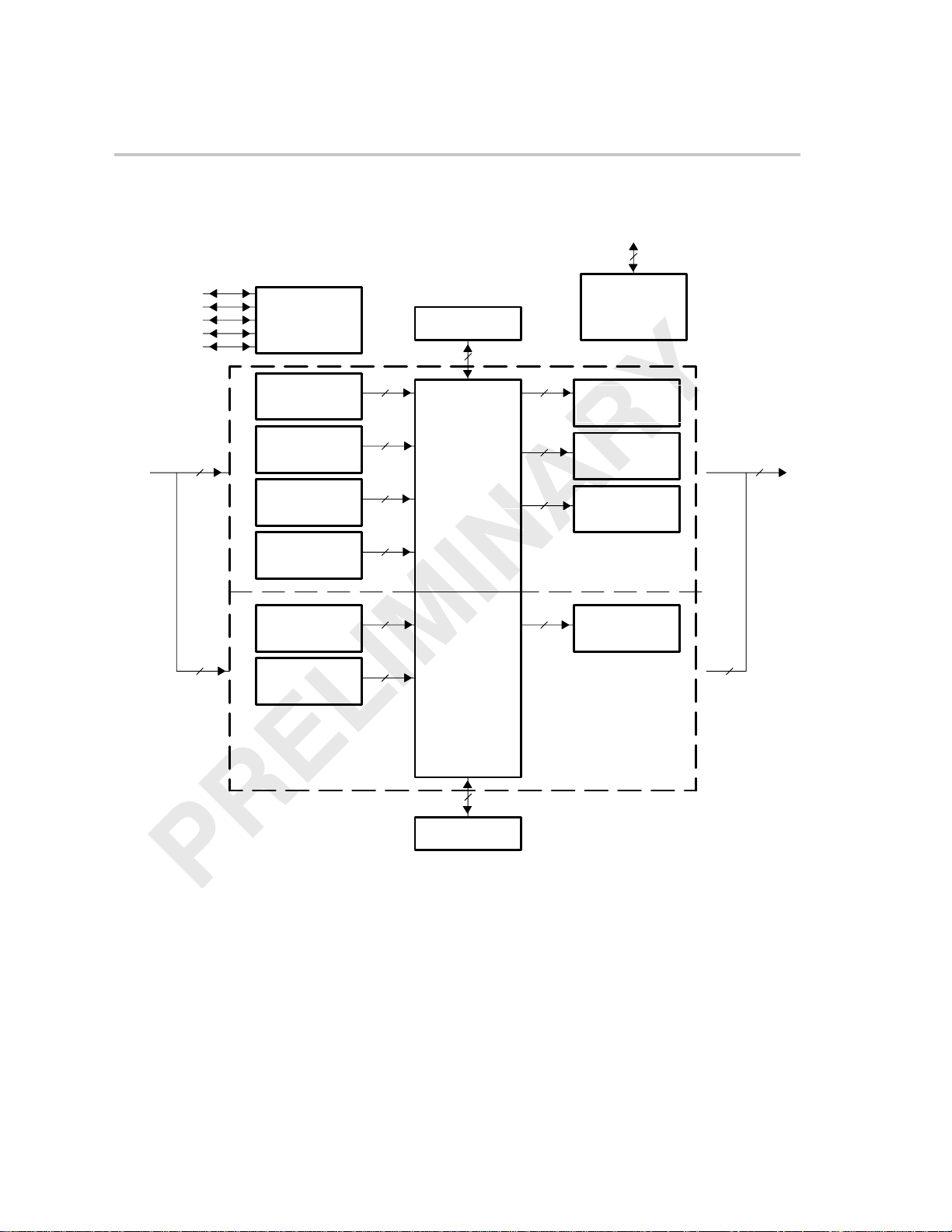
Figure 1–1. Video Port Block Diagram
VCLK1
VCLK2
VCTL1
VCTL2
VCTL3
Timing and
control logic
DMA interface
64
Internal peripheral bus
32
Memory
mapped
registers
VDIN[19–0]
20
10
VDIN[19–10]
BT.656 capture
pipeline
Y/C video
capture pipeline
Raw video
capture pipeline
TSI capture
pipeline
BT.656 capture
pipeline
Raw video
capture pipeline
10 10
20
Capture/display
(2560 bytes)
20
8
10
Capture/display
10
(2560 bytes)
DMA interface
buffer
buffer
64
20
20
10
BT.656 display
pipeline
Y/C video
display pipeline
Raw video
display pipeline
Channel A
Raw video
display pipeline
Channel B
VDOUT[19–0]
20
10
VDOUT[19–10]
Overview1-4 SPRU629
Page 22

1.2 Video Port FIFO
The video port includes a FIFO to store data coming into or out from the video
port. The video port operates in conjunction with DMA transfers to move data
between the video port FIFO and external or on-chip memory. You can program threshold settings so DMA events are generated when the video port
FIFO reaches a certain fullness (for capture) or goes below a certain fullness
(for display). DMAs required to service the FIFO are set up independently by
you and are key to correct operation of the video port. The FIFO size is relatively large to allow time for DMAs to service the transfer requests, since devices
typically have many peripheral interfaces often including multiple video ports.
The following sections briefly describe the interaction with the DMA and different FIFO configurations used to support the various modes of the video port.
1.2.1 DMA Interface
Video port data transfers take place using DMAs. DMA requests are based on
buffer thresholds. Since the video port does not directly source the transfer , it
can not adjust the transfer size based on buffer empty/full status. This means
the DMA transfer size is essentially fixed in the user-programmed DMA
parameter table. The preferred transfer size is often one entire line of data,
because this allows the most flexibility in terms of frame buffer line pitch (in
RAM). Some modes of operation for the highest display rates may require
more frequent DMA requests such as on a half or quarter line basis.
Video Port FIFO
All requests are based on buffer thresholds. In video capture mode, DMA
requests are made whenever the number of samples in the buffer reaches the
threshold value. In order to ensure that all data from a capture field/frame gets
emptied from the buffer , the transfer size must be equal to the threshold and
the total amount of field/frame data must be a multiple of the transfer size.
For video display operation, DMA requests are made whenever there is at
least the threshold number of doublewords free in the FIFO. This means that
the transfer size must be equal to or smaller than the threshold so that it fits
into the available space. The field/frame size must still be a multiple of the
transfer size or there are pixels left in the buffer at the end of the field (which
appear at the start of the next field).
1-5OverviewSPRU629
Page 23
Video Port FIFO
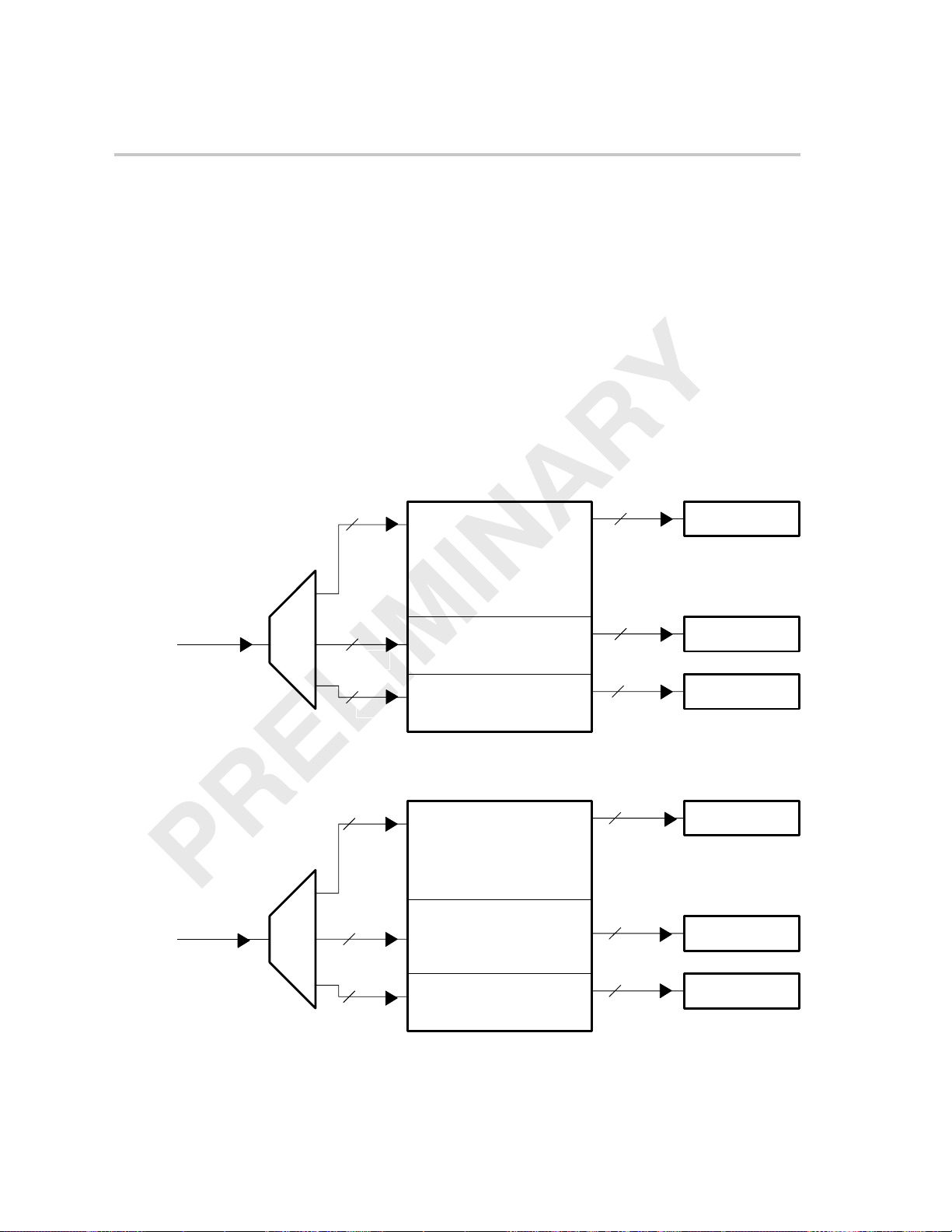
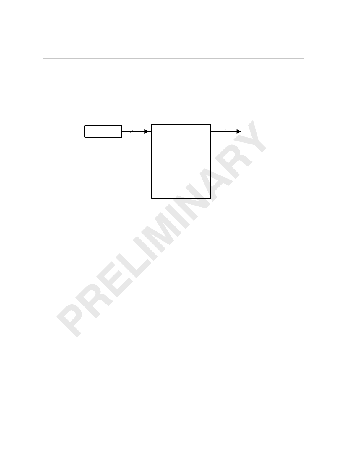
1.2.2 Video Capture FIFO Configurations
During video capture operation, the video port FIFO has one of four configurations depending on the capture mode. For BT.656 operation, the FIFO is split
into channel A and B, as shown in Figure 1–2. Each FIFO is clocked independently with the channel A FIFO receiving data from the VDIN[9–0] half of the
bus and the channel B FIFO receiving data from the VDIN[19–10] half of the
bus. Each channel’s FIFO is further split into Y, Cb, and Cr buffers with separate write pointers and read registers (YSRCx, CBSRCx, and CRSRCx).
Figure 1–2. BT.656 Video Capture FIFO Configuration
Capture FIFO A
VDIN[9–0]
VDIN[19–10]
8/10
8/10
8/10
8/10
8/10
Y Buffer A (1280 bytes)
Cb Buffer A (640 bytes)
Cr Buffer A (640 bytes)
Capture FIFO B
Y Buffer B (1280 bytes)
Cb Buffer B (640 bytes)
64
64
64
64
64
YSRCA
CBSRCA
CRSRCA
YSRCB
CBSRCB
8/10
Overview1-6 SPRU629
Cr Buffer B (640 bytes)
64
CRSRCB
Page 24
Video Port FIFO
For 8/10-bit raw video, the FIFO is split into channel A and B, as shown in
Figure 1–3. Each FIFO is clocked independently with the channel A FIFO
receiving data from the VDIN[9–0] half of the bus and the channel B FIFO
receiving data from the VDIN[19–10] half of the bus. Each channel’s FIFO has
a separate write pointer and read register (YSRCx). The FIFO configuration
is identical for TSI capture, but channel B is disabled.
Figure 1–3. 8/10-Bit Raw Video Capture and TSI Video Capture FIFO Configuration
Capture FIFO A
VDIN[9–0]
8/10
64
Buffer A (2560 bytes)
YSRCA
VDIN[19–10]
8/10
Capture FIFO B
Buffer B (2560 bytes)
64
YSRCB
1-7OverviewSPRU629
Page 25
Video Port FIFO
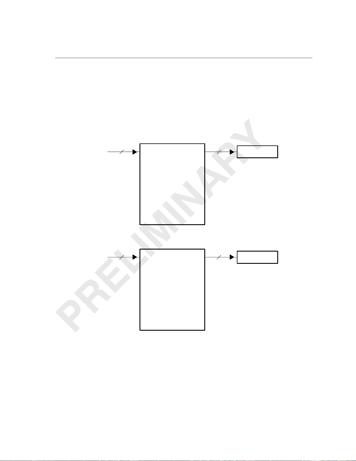
For Y/C video capture, the FIFO is configured as a single channel split into separate Y, Cb, and Cr buffers with separate write pointers and read registers
(YSRCA, CBSRCA, and CRSRCA). Figure 1–4 shows how Y data is received
on the VDIN[9–0] half of the bus and Cb/Cr data is received on the
VDIN[19–10] half of the bus and demultiplexed into the Cb and Cr buffers.
Figure 1–4. Y/C Video Capture FIFO Configuration
Capture FIFO
VDIN[9–0]
VDIN[19–10]
8/10
8/10
8/10
Y Buffer (2560 bytes)
Cb Buffer (1280 bytes)
Cr Buffer (1280 bytes)
64
64
64
YSRCA
CBSRCA
CRSRCA
Overview1-8 SPRU629
Page 26

For 16/20-bit raw video, the FIFO is configured as a single buffer, as shown
in Figure 1–5. The FIFO receives 16/20-bit data from the VDIN[19–0] bus. The
FIFO has a single write pointer and read register (YSRCA).
Figure 1–5. 16/20-Bit Raw Video Capture FIFO Configuration
Capture FIFO
VDIN[19–0]
16/20
Data Buffer
(5120 bytes)
64
Video Port FIFO
YSRCA
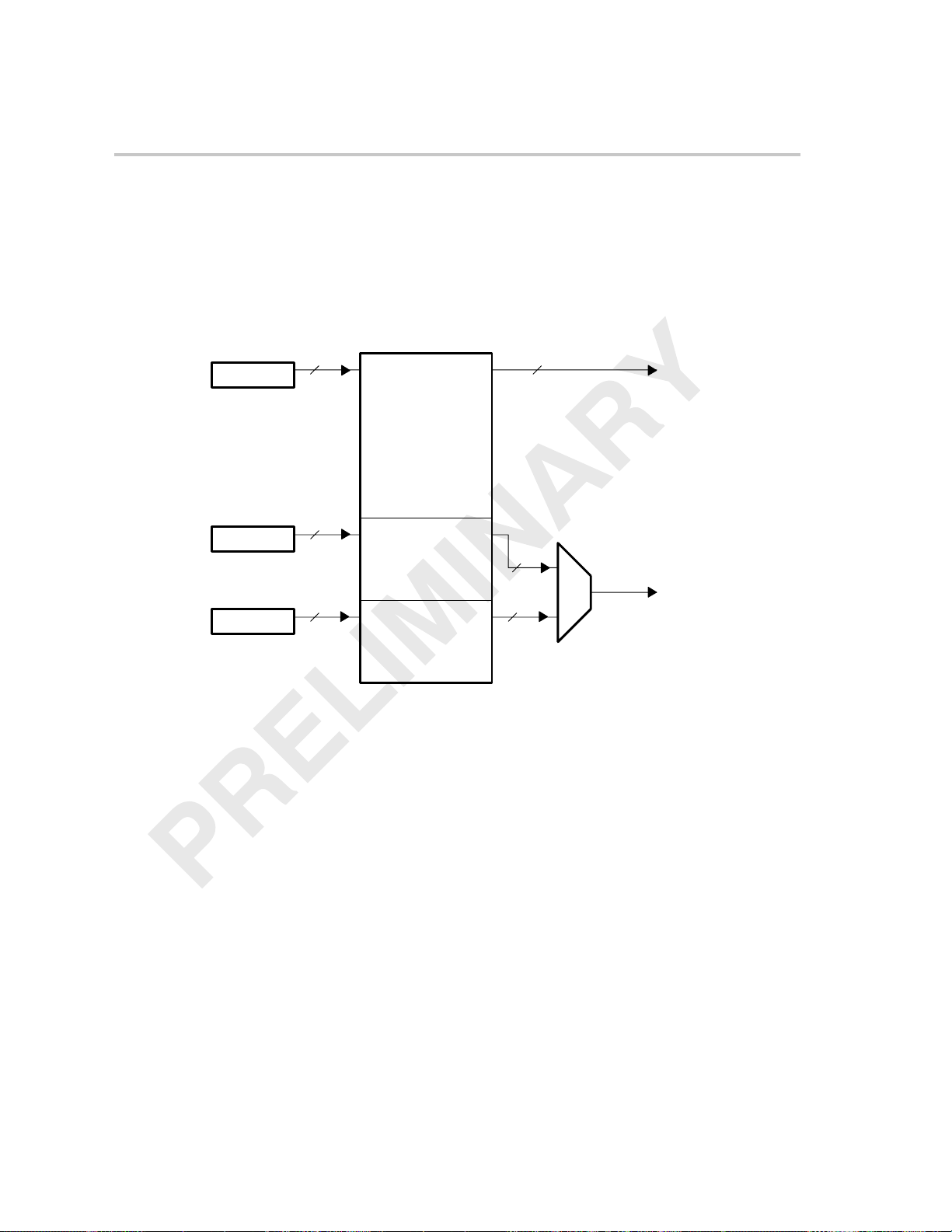
1.2.3 Video Display FIFO Configurations
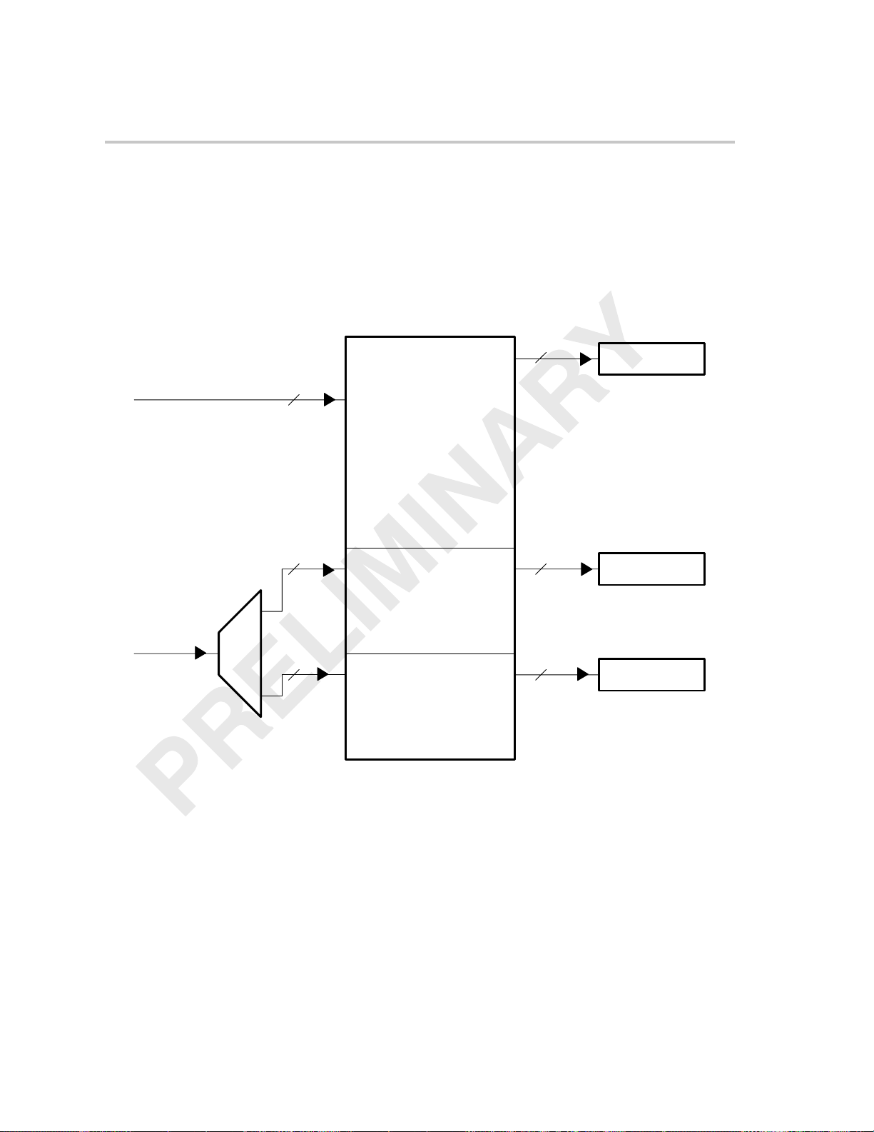
During video display operation, the video port FIFO has one of five configurations depending on the display mode. For BT.656 operation, a single output
is provided on channel A, as shown in Figure 1–6, with data output on
VDOUT[9–0]. The channel’s FIFO is split into Y, Cb, and Cr buffers with
separate read pointers and write registers (YDSTA, CBDST, and CRDST).
Figure 1–6. BT.656 Video Display FIFO Configuration
Display FIFO
YDSTA
CBDST
CRDST
64
64
64
Y Buffer
(2560 bytes)
Cb Buffer
(1280 bytes)
Cr Buffer
(1280 bytes)
8/10
VDOUT[9–0]
8/10
8/10
1-9OverviewSPRU629
Page 27
Video Port FIFO
For 8/10-bit raw video, the FIFO is configured as a single buffer as shown in
Figure 1–7. The FIFO outputs data on the VDOUT[9–0] half of the bus. The
FIFO has a single read pointer and write register (YDSTA).
Figure 1–7. 8/10-Bit Raw Video Display FIFO Configuration
Display FIFO
YDSTA
64
Data Buffer
(5120 bytes)
For locked raw video, the FIFO is split into channel A and B. The channels are
locked together and use the same clock and control signals. Each channel
uses a single buffer and write register (YDSTx) as shown in Figure 1–8.
VDOUT[9–0]
8/10
Overview1-10 SPRU629
Page 28
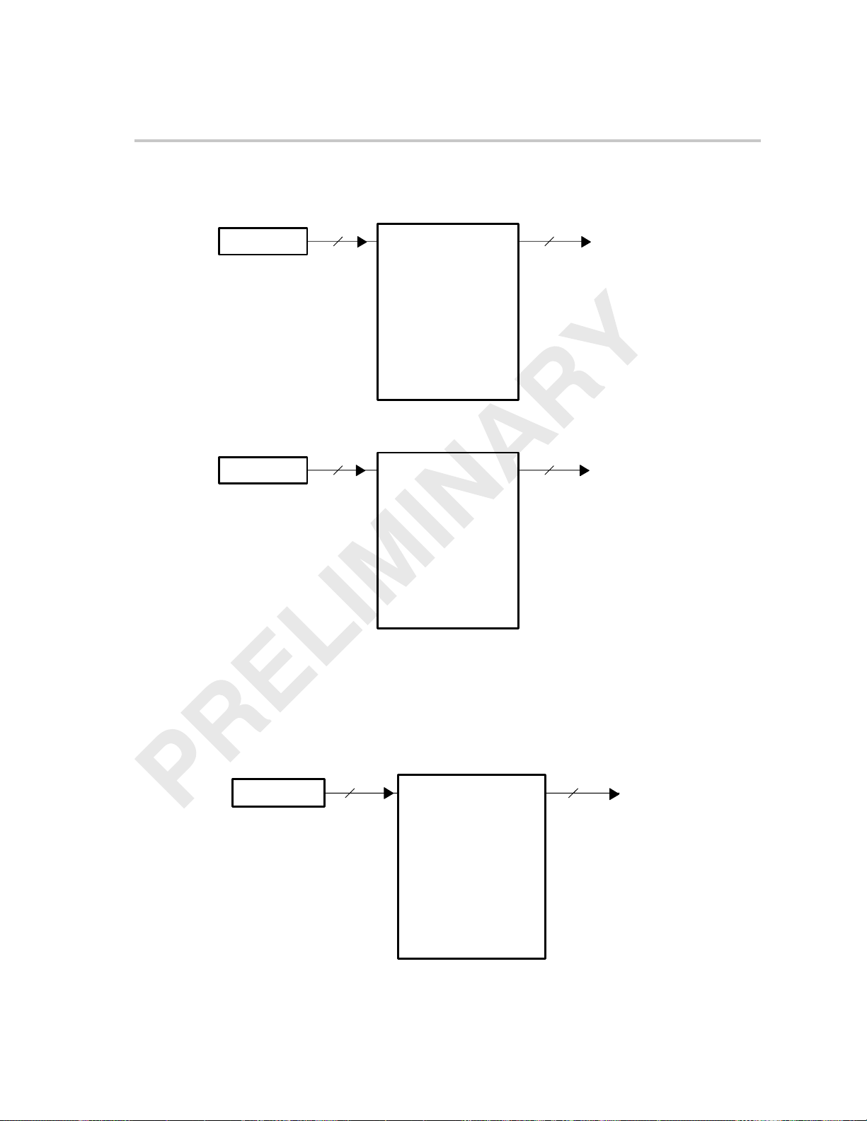
Figure 1–8. 8/10 Bit Locked Raw Video Display FIFO Configuration
Display FIFO A
YDSTA
YDSTB
64 8/10
Buffer A (2560 bytes)
Display FIFO B
64 8/10
Buffer B (2560 bytes)
VDOUT[9–0]
VDOUT[19–10]
Video Port FIFO
For 16/20-bit raw video, the FIFO is configured as a single buffer, as shown
in Figure 1–9. The FIFO outputs data on VDOUT[19–0]. The FIFO has a single
read pointer and write register (YDSTA).
Figure 1–9. 16/20-Bit Raw Video Display FIFO Configuration
Display FIFO
YDSTA
64 16/20
Data Buffer (5120 bytes)
VDOUT[19–0]
1-11OverviewSPRU629
Page 29
Video Port Registers
Video Port FIFO / Video Port Registers
For Y/C video display , the FIFO is configured as a single channel split into separate Y, Cb, and Cr buffers with separate read pointers and write registers
(YDSTA, CBDST, and CRDST). Figure 1–10 shows how Y data is output on
the VDOUT[9–0] half of the bus and Cb/Cr data is multiplexed and output on
the VDOUT[19–10] half of the bus.
Figure 1–10. Y/C Video Display FIFO Configuration
Display FIFO
YDSTA
64
Y Buffer
(2560 bytes)
VDOUT[9–0]
8/10
CBDST
CRDST
64
64
1.3 Video Port Registers
The video port configuration register space is divided into several different
sections with registers grouped by function including top-level video port
control, video capture control, video display control, and GPIO.
The registers for controlling the video port are in section 2.7.
The registers for controlling the video capture mode of operation are shown
in section 3.13. An additional space is dedicated for FIFO read pseudo-registers
as shown in section 3.14. This space requires high-speed access and is not
mapped to the register access bus.
The registers for controlling the video display mode of operation are shown in
section 4.12. An additional space is dedicated for FIFO write pseudo-registers
as shown in section 4.14. This space requires high-speed access and is not
mapped to the register access bus.
Cb Buffer
(1280 bytes)
Cr Buffer
(1280 bytes)
8/10
8/10
VDOUT[19–10]
The registers for controlling the general-purpose input/output (GPIO) are
shown in section 5.1.
Overview1-12 SPRU629
Page 30

1.4 Video Port Pin Mapping
The video port requires 21 external signal pins for full functionality . Pin usage
and direction changes depend on the selected operating mode. Pin functionality detail for video capture mode is listed in Table 1–1. Pin functionality detail
for video display mode is listed in Table 1–2. All unused port signals (except
VCLK1 and VCLK2) can be configured as general-purpose I/O (GPIO) pins.
Table 1–1. Video Capture Signal Mapping
BT.656 Capture Mode Raw Data Capture Mode
Video Port
Signal
VDATA[9–0]
I/O
I/O VDIN[9–0]
Dual
Channel
(In) Ch A
Single
Channel
VDIN[9–0]
(In) Ch A
Usage
Y/C Capture
Mode
VDIN[9–0]
(In) (Y)
8/10-Bit
VDIN[9–0]
(In) Ch A
Video Port Pin Mapping
TSI Capture
16/20-Bit
VDIN[9–0]
(In)
Mode
VDIN[7–0]
(In)
VDATA[19–10]
VCLK1
VCLK2
VCTL1
VCTL2
VCTL3
Legend: VCLKINA – Channel A capture clock; CAPENA – Channel A capture enable; VCLKINB – Channel B capture clock;
CAPENB – Channel B capture enable; A VID – Active video; HSYNC – Horizontal synchronization; VBLNK – Vertical
blanking; VSYNC – Vertical synchronization; FID – Field identification; PACSTRT – Packet start; PACERR – Packet
error
I/O VDIN[19–10]
(In) Ch B
I VCLKINA (In) VCLKINA (In) VCLKINA (In) VCLKINA (In) VCLKINA (In) VCLKINA (In)
I/O VCLKINB (In) Not Used Not Used VCLKINB (In) Not Used Not Used
I/O CAPENA
(In)
I/O CAPENB
(In)
I/O Not Used FID
Not Used VDIN[19–10]
CAPENA/
AVID/HSYNC
(In)
VBLNK/
VSYNC (In)
(In)
(In) (Cb/Cr)
CAPENA/
AVID/HSYNC
(In)
VBLNK/
VSYNC (In)
FID
(In)
VDIN[19–10]
(In) Ch B
CAPENA
(In)
CAPENB
(In)
FID (In)
Ch A
VDIN[19–10]
(In)
CAPENA
(In)
Not Used PACSTRT
FID (In)
Ch A
Not Used
CAPENA
(In)
(In)
PACERR
(In)
1-13OverviewSPRU629
Page 31

Video Port Pin Mapping
Table 1–2. Video Display Signal Mapping
Video Port
Signal
VDATA[9–0] I/O VDOUT[9–0]
I/O
BT.656
Display Mode
(Out)
Y/C Display
Mode
VDOUT[9–0]
(Out) (Y)
Usage
8/10-Bit
VDOUT[9–0]
(Out)
Raw Data Display Mode
16/20-Bit
VDOUT[9–0]
(Out)
8/10-Bit
Dual Sync
VDOUT[9–0]
(Out) (Ch A)
VDATA[19–10] I/O Not Used VDOUT[19–10]
VCLK1 I VCLKIN (In) VCLKIN (In) VCLKIN (In) VCLKIN (In) VCLKIN (In)
VCLK2 I/O VCLKOUT (Out) VCLKOUT (Out) VCLKOUT (Out) VCLKOUT (Out) VCLKOUT (Out)
VCTL1 I/O HSYNC/HBLNK/
VCTL2 I/O VSYNC/VBLNK/
VCTL3
AVID/FLD (Out)
or HSYNC (In)
CSYNC/FLD (Out)
or VSYNC (In)
I/O CBLNK/FLD (Out)
or FLD (In)
(Out) (Cb/Cr)
HSYNC/HBLNK/
AVID/FLD (Out)
or HSYNC (In)
VSYNC/VBLNK/
CSYNC/FLD (Out)
or VSYNC (In)
CBLNK/FLD (Out)
or FLD (In)
Not Used VDOUT[19–10]
HSYNC/HBLNK/
AVID/FLD (Out)
or HSYNC (In)
VSYNC/VBLNK/
CSYNC/FLD (Out)
or VSYNC (In)
CBLNK/FLD (Out)
or FLD (In)
HSYNC/HBLNK/
AVID/FLD (Out)
or HSYNC (In)
VSYNC/VBLNK/
CSYNC/FLD (Out)
or VSYNC (In)
CBLNK/FLD (Out)
or FLD (In)
(Out)
VDOUT[9–0]
(Out) (Ch B)
HSYNC/HBLNK/
AVID/FLD (Out)
or HSYNC (In)
VSYNC/VBLNK/
CSYNC/FLD (Out)
or VSYNC (In)
CBLNK/FLD (Out)
or FLD (In)
Overview1-14 SPRU629
Page 32

Video Port Pin Mapping
1.4.1 VDIN Bus Usage for Capture Modes
The alignment and usage of data on the VDIN bus depends on the capture
mode as shown in Table 1–3.
Table 1–3. VDIN Data Bus Usage for Capture Modes
Capture Mode
BT.656 Y/C Raw Data
Data Bus 10-Bit 8-Bit 10-Bit 8-Bit 8-Bit 10-Bit 16-Bit 20-Bit
TSI
Mode
VDIN19
VDIN18 B B A (C) A (C) BBAA
VDIN17 B B A (C) A (C) BBAA
VDIN16 B B A (C) A (C) BBAA
VDIN15 B B A (C) A (C) BBAA
VDIN14 B B A (C) A (C) BBAA
VDIN13 B B A (C) A (C) BBAA
VDIN12 B B A (C) A (C) BBAA
VDIN11 B A (C) B A
VDIN10 B A (C) B A
VDIN9 A A A (Y) A (Y) AAAAA
VDIN8 A A A (Y) A (Y) AAAAA
VDIN7 A A A (Y) A (Y) AAAAA
VDIN6 A A A (Y) A (Y) AAAAA
VDIN5 A A A (Y) A (Y) AAAAA
B B A (C) A (C) B B A A
VDIN4 A A A (Y) A (Y) AAAAA
VDIN3 A A A (Y) A (Y) AAAAA
VDIN2 A A A (Y) A (Y) AAAAA
VDIN1 A A (Y) A A
VDIN0
Legend: A – Channel A capture; A(C) Channel A chroma; A(Y) Channel A luma; B – Channel B capture
A A (Y) A A
1-15OverviewSPRU629
Page 33

Video Port Pin Mapping
1.4.2 VDOUT Data Bus Usage for Display Modes
The alignment and usage of data on the VDOUT bus depends on the display
mode as shown in Table 1–4.
Table 1–4. VDOUT Data Bus Usage for Display Modes
Display Mode
BT.656 Y/C Dual Sync Raw Data Raw Data
Data Bus 10-Bit 8-Bit 10-Bit 8-Bit 8-Bit 10-Bit 16-Bit 20-Bit
VDOUT19 A (C) A (C) (B) (B) A A
VDOUT18 A (C) A (C) (B) (B) A A
VDOUT17 A (C) A (C) (B) (B) A A
VDOUT16 A (C) A (C) (B) (B) A A
VDOUT15 A (C) A (C) (B) (B) A A
VDOUT14 A (C) A (C) (B) (B) A A
VDOUT13 A (C) A (C) (B) (B) A A
VDOUT12 A (C) A (C) (B) (B) A A
VDOUT11 A (C) (B) A
VDOUT10 A (C) (B) A
VDOUT9 A A A (Y) A (Y) A A A A
VDOUT8 A A A (Y) A (Y) A A A A
VDOUT7 A A A (Y) A (Y) A A A A
VDOUT6 A A A (Y) A (Y) A A A A
VDOUT5 A A A (Y) A (Y) A A A A
VDOUT4 A A A (Y) A (Y) A A A A
VDOUT3 A A A (Y) A (Y) A A A A
VDOUT2 A A A (Y) A (Y) A A A A
VDOUT1 A A (Y) A A
VDOUT0
Legend: A – Channel A display; A(C) Channel A chroma; A(Y) Channel A luma; B – Optional locked channel B display
A A (Y) A A
Overview1-16 SPRU629
Page 34

Chapter 2
Video Port
This chapter discusses the basic operation of the video port. Included is a
discussion of the sources and types of resets, interrupt operation, DMA operation, external clock inputs, video port throughput and latency, and the video
port control registers.
Topic Page
2.1 Reset Operation 2-2. . . . . . . . . . . . . . . . . . . . . . . . . . . . . . . . . . . . . . . . . . . . . .
2.2 Interrupt Operation 2-5. . . . . . . . . . . . . . . . . . . . . . . . . . . . . . . . . . . . . . . . . . . .
2.3 DMA Operation 2-6. . . . . . . . . . . . . . . . . . . . . . . . . . . . . . . . . . . . . . . . . . . . . . .
2.4 Clocks 2-12. . . . . . . . . . . . . . . . . . . . . . . . . . . . . . . . . . . . . . . . . . . . . . . . . . . . . .
2.5 Video Port Functionality Subsets 2-12. . . . . . . . . . . . . . . . . . . . . . . . . . . . . .
2.6 Video Port Throughput and Latency 2-13. . . . . . . . . . . . . . . . . . . . . . . . . . .
2.7 Video Port Control Registers 2-16. . . . . . . . . . . . . . . . . . . . . . . . . . . . . . . . . .
2-1
Page 35

Reset Operation
2.1 Reset Operation
The video port has several sources and types of resets. The actions performed
by these resets and the state of the port following the resets is described in the
following sections.
2.1.1 Power-On Reset
Power-on reset is an asynchronous hardware reset caused by a chip-level
reset operation. The reset is initiated by a power-on reset input to the video
port. When the input is active, the port places all I/Os (VD[19–0], VCTL1,
VCTL2, VCTL3, and VCLK2) in a high-impedance state.
2.1.2 Peripheral Bus Reset
Peripheral bus reset is a synchronous hardware reset caused by a chip-level
reset operation. The reset is initiated by a peripheral bus reset input to the video
port. This reset can be used internally (continuously asserted) to disable the
video port for low-power operation. When the input is active, the port does the
following:
- Places (keeps) all I/Os (VD[19–0], VCTL1, VCTL2, VCTL3, and VCLK2)
in a high-impedance state.
- Flushes the FIFOs (resets pointers)
- Resets all port, capture, display, and GPIO registers to their default
values. These may not complete until the appropriate module clock
(VCLK1, VCLK2, STCLK) edges occur to synchronously release the logic
from reset.
- Clears PEREN bit in PCR to 0.
- Sets VPHLT bit in VPCTL to 1.
While the peripheral remains disabled (PEREN = 0):
- VCLK1, VCLK2, and STCLK are gated off to save peripheral power.
- Peripheral bus accesses are acknowledged (RREADY/WREADY
returned) to prevent DMA lock-up. (Any value returned on reads, data
accepted or discarded on writes.)
- Peripheral bus MMR interface allows access to GPIO registers only (PID,
PCR, PFUNC, PDIR, PIN, PDOUT, PDSET, PDCLR, PIEN, PIPOL,
PISTAT, and PICLR).
- Port I/Os (VD[19–0], VCTL1, VCTL2, VCTL3, and VCLK2) remain in a
high-impedance state unless enabled as GPIO by the PFUNC bits.
Video Port2-2 SPRU629
Page 36

If software sets the PEREN bit in PCR but the VPHLT bit in VPCTL remains
set:
- VCLK1, VCLK2, and STCLK are enabled to the port (allowing logic reset
to complete).
- Peripheral bus accesses are acknowledged (RREADY/WREADY
returned) to prevent DMA lock-up. (Any value returned on reads, data
accepted or discarded on writes.)
- Peripheral bus MMR interface allows access to all registers.
- Port I/Os (VD[19–0], VCTL1, VCTL2, VCTL3, and VCLK2) remain in a
high-impedance state unless enabled as GPIO by the PFUNC bits.
- VPCTL bits may be set (until the VPHLT bit is cleared).
2.1.3 Software Port Reset
A software port reset may be performed on the entire video port by setting the
VPRST bit in VPCTL. This behaves identically to the peripheral bus reset
except that it does not clear the PEREN bit in PCR. This reset:
- Performs an asynchronous reset on all port logic (channel logic may stay
in reset until port input clock pulses occur).
Reset Operation
- Self-clears the VPRST bit to 0 but leaves the VPHLT bit set.
Once the port is configured and the VPHL T bit is cleared, the setting of other
VPCTL bits (except VPRST) is disabled. The VCLK2 output may also be driven
at this time, if display mode is selected. VCTL1–3 must remain in a high-impedance state unless enabled as GPIO, since internal/external sync is selected
through VDCTL.
2.1.4 Capture Channel Reset
A software reset may be performed on a single capture channel by setting the
RSTCH bit in VCxCTL. This reset requires that the channel VCLKIN be transitioning. On capture channel reset:
- No new DMA events are generated.
- Peripheral bus accesses are acknowledged (RREADY returned) to prevent
DMA lock-up. (Any value returned on reads)
- Channel capture registers are set to their default values.
- Channel capture FIFO is flushed (pointers reset).
- The VCEN bit in VCxCTL is cleared to 0.
- The RSTCH bit self-clears to 0 after completion of the above.
2-3Video PortSPRU629
Page 37

Reset Operation
Once the port is configured and the VCEN bit is set, the setting of other
VCxCTL bits (except VCEN, RSTCH, and BLKCAP) is prohibited and the
capture counters begin counting. When BLKCAP is cleared, data capture and
event generation may begin.
2.1.5 Display Channel Reset
A software reset may be performed on the display channel by setting the
RSTCH bit in VDCTL. This reset requires that the channel VCLKIN be transitioning. On display channel reset:
- No new DMA events are generated.
- Peripheral bus accesses are acknowledged (WREADY returned) to prevent
DMA lock-up. (Write data may be written into the FIFO or discarded.)
- Channel display registers are set to their default values.
- Channel display FIFO is flushed (pointers reset).
- The VDEN bit in VDCTL is cleared to 0.
- The RSTCH bit self-clears to 0 after completion of the above.
Once the port is configured and the VDEN bit is set, the setting of other VDCTL
bits (except VDEN, RSTCH, and BLKDIS) is prohibited and the display counters
begin counting. Data outputs are driven (with default value, blanking, and
control codes as appropriate and any control outputs are driven). When the
BLKDIS bit is cleared, event generation may begin and FIFO data displayed.
Video Port2-4 SPRU629
Page 38

2.2 Interrupt Operation
The video port can generate an interrupt to the DSP core after any of the following events occur:
- Capture complete (CCMPx) bit is set.
- Capture overrun (COVRx) bit is set.
- Synchronization byte error (SERRx) bit is set.
- Vertical interrupt (VINTxn) bit is set.
- Short field detect (SFDx) bit is set.
- Long field detect (LFDx) bit is set.
- STC absolute time (STC) bit is set.
- STC tick counter expired (TICK) bit is set.
- Display complete (DCMP) bit is set.
- Display underrun (DUND) bit is set.
- Display complete not acknowledged (DCNA) bit is set.
- GPIO interrupt (GPIO) bit is set.
The interrupt signal is a pulse only and does not hold state. The interrupt pulse
is generated only when the number of set flags in VPIS transitions from none
to one or more. Another interrupt pulse is not generated by setting additional
flag bits.
Interrupt Operation
Interrupts can be masked via the video port interrupt enable register (VPIE)
using individual interrupt enables and the VIE global enable bit. The interrupts
are cleared in the video port interrupt status register (VPIS) using the individual
status bits. Writing a 1 to the appropriate bit clears the interrupt. The clearing
of an interrupt flag reenables the generation of another interrupt pulse, if other
flags are still set. In other words, pulse generation is reenabled by writing a 1
to any set bit of VPIS.
Upon receiving an interrupt you should:
1) Read VPIS.
2) Perform the service routine for whatever bits are set.
3) Clear appropriate bits by writing a 1 to their VPIS locations.
4) Upon return from the ISR, if VPIS bits have been (or remain) set, then
another interrupt will occur.
2-5Video PortSPRU629
Page 39

DMA Operation
2.3 DMA Operation
The video port uses up to three DMA events per channel for a total of six
possible events. Each DMA event uses a dedicated event output. The outputs
are:
- VPYEVTA
- VPCbEVTA
- VPCrEVTA
- VPYEVTB
- VPCbEVTB
- VPCrEVTB
2.3.1 Capture DMA Event Generation
Capture DMA events are generated based on the state of the capture FIFO(s).
If no DMA event is currently pending and the FIFO crosses the value specified
by VCTHRLDn, a DMA event is generated. Once an event has been
requested, another DMA event may not be generated until the servicing of the
outstanding event has begun (as indicated by the first read of the FIFO by the
DMA event service). If the capture FIFO level exceeds 2× the VCTHRLDn
value before the requested DMA event completes, then another DMA event
may be generated. Thus, up to one DMA event may be outstanding.
An outgoing data counter counts data read by the DMA. This counter is loaded
with the VCTHRLDn value whenever a new DMA service begins. The counter
then counts down for each double-word read from the FIFO by the DMA. The
DMA is complete when the counter reaches zero. Figure 2–1 shows the
capture DMA event generation.
For BT.656 and Y/C modes, there are three FIFOs, one for each of the Y , Cb,
and Cr color components. Each FIFO generates its own DMA event; therefore,
the DMA event state and FIFO thresholds for each FIFO are tracked independently. The Cb and Cr FIFOs use a threshold value of
½ (VCTHRLDn + VCTHRLDn mod 2).
Video Port2-6 SPRU629
Page 40

Figure 2–1. Capture DMA Event Generation Flow Diagram
Empty FIFO
Capture data, no
DMA pending
DMA Operation
No
FIFO ≥ threshold
?
Yes
Generate DMA event
Capture data, DMA pend-
ing, new events disabled
Pending DMA begun
?
Yes
Capture data, DMA active,
new events enabled
FIFO ≥ 2x threshold
?
Yes
No
No
No
FIFO overflow
Yes
DMA complete
?
Yes
?
No
No
FIFO overflow
Error
?
Yes
Generate DMA request
Capture Data, DMA
active & DMA pending
Yes
DMA complete
?
No
No
FIFO overflow
?
Yes
Overflow error
Overflow error
2-7Video PortSPRU629
Page 41

DMA Operation
Because the capture FIFOs may hold multiple thresholds worth of data, a
problem arises at the boundaries between fields. Since Field 1 and Field 2
may have different threshold values, the amount of data in the FIFO required
to generate the DMA event changes depending on the current capture field
and the field of any outstanding DMA requests. Similarly , the threshold value
loaded in the outgoing data counter needs to change depending on which
field’s DMA event is being serviced (not which field is currently being
captured). T o prevent confusion at the field boundaries, the VCxEVTCT register is programmed to indicate the number of events to generate for each field.
An event counter tracks how many events have been generated and indicates
which threshold value to use in event generation and in the outgoing data
counter. After the last Field 1 event has been generated, the DMA logic looks
for FIFO > THRSHLD1 + THRSHLD2 to pregenerate the first Field 2 event.
Once the last Field 1 event completes, the logic looks for
FIFO > 2 × THRSHLD2 (assuming a Field 2 event is outstanding).
Some initial devices may require THRSHLD1 and THRSHLD2 to be set to the
same value. Check the latest device errata, if you want to use different thresholds for the two fields.
2.3.2 Display DMA Event Generation
Display DMA events are generated based on the amount of room available in
the FIFO. The VDTHRLDn value indicates the level at which the FIFO has
room to receive another DMA. If the FIFO has at least VDTHRLDn locations
available, a DMA event is generated. Once a DMA event has been requested,
another DMA event may not be generated until the servicing of the first DMA
event has begun (as indicated by the first write to the FIFO by the DMA event
service). If there is at least 2× the threshold space still available in the FIFO
after the first DMA service is begun (and the display event counter has not
expired) then another DMA event may be generated. Thus, up to one DMA
request may be outstanding.
An incoming data counter is loaded with the VDTHRLDn (or VDTHRLDn/2 for
Cb and Cr FIFOs) value at the beginning of each DMA event service and
counts down the incoming DMA doublewords When the counter reaches 0, the
DMA event is complete. Figure 2–2 shows the display DMA event generation.
Video Port2-8 SPRU629
Page 42
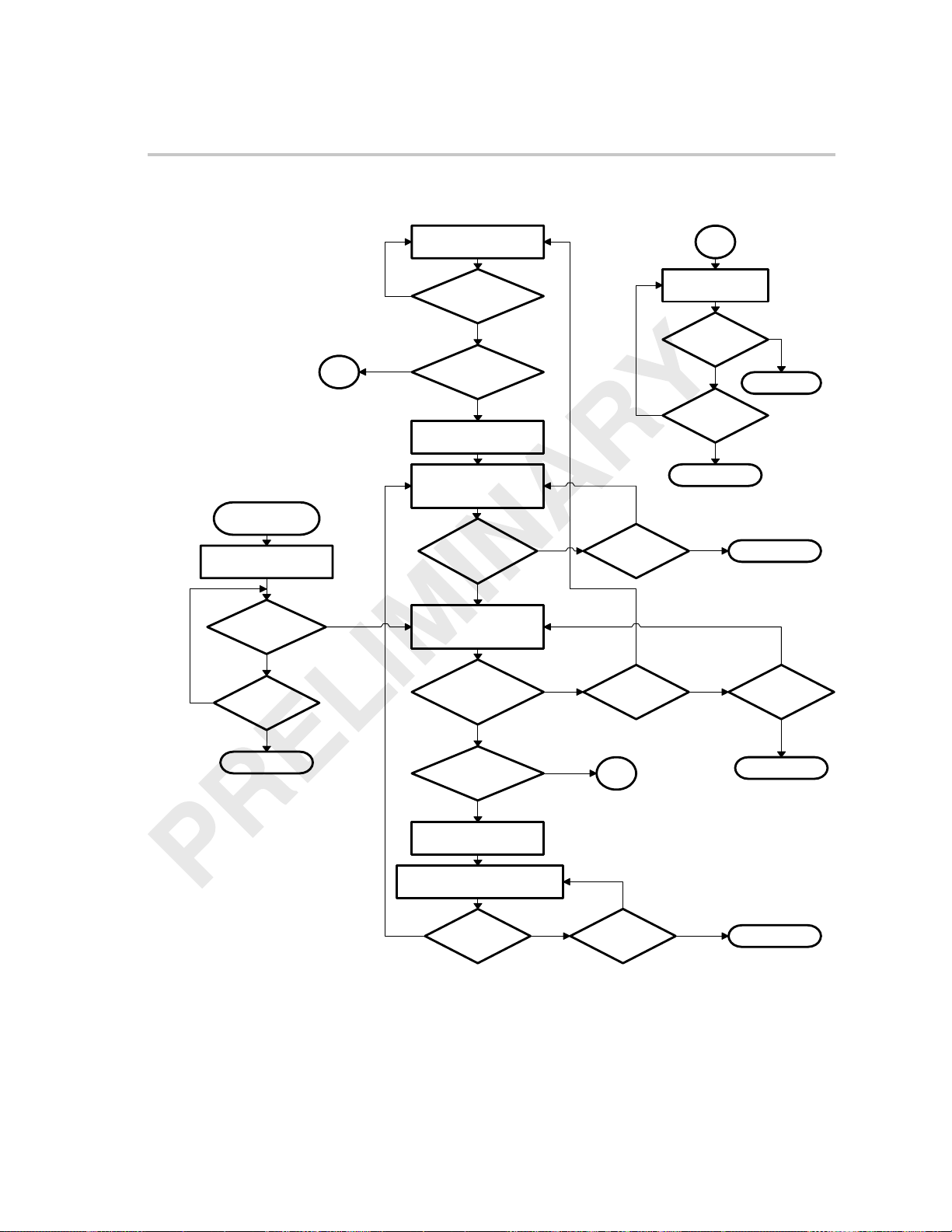
Figure 2–2. Display DMA Event Generation Flow Diagram
DMA Operation
Start of field
FIFO empty
Generate DMA event,
new events disabled
Pending
DMA begun ?
No
FIFO
underrun ?
No
Yes
Underrun error
EOF
Yes
Display data, no DMA
pending
No
Yes
FIFO space
threshold
Yes
Event counter
expired ?
No
Generate DMA event
Display data, DMA
pending, new events
disabled
Pending DMA
begun ?
Yes
Display data, DMA
active, new events
enabled
FIFO space
2x threshold
Yes
Event counter
expired ?
EOF
Display data
?
Field complete
?
No
No
FIFO underrun
?
Yes
Underrun error
No
No
FIFO underrun
?
Yes
No No
DMA complete
?
Yes
?
EOF
Yes
Yes
End of field
Underrun error
No
FIFO underrun
?
Yes
Underrun error
No
Generate DMA
request
Display Data, DMA active,
and DMA pending
Yes
DMA complete
?
No
No
FIFO underrun
?
Yes
Underrun error
2-9Video PortSPRU629
Page 43

DMA Operation
A DMA event counter is used to track the number of DMA events generated
in each field as programmed in the VDDISPEVT register. The DISPEVT1 or
DISPEVT2 value (depending on the current display field) is loaded at the start
of each field. The event counter then decrements with each DMA event generation until it reaches 0, at which point no more DMA events are generated until
the next field begins. Once the last line of data for a field has been requested,
the DMA logic stops generating events until the field is complete in case the
CPU needs to modify the DMA address pointers.
For BT.656 and Y/C modes, there are three FIFOs, one for each of the Y , Cb,
and Cr color components. Each FIFO generates its own DMA event; therefore,
the DMA event state and FIFO thresholds for each FIFO are tracked independently. (The Cb and Cr FIFOs use a threshold value of ½ VDTHRLD).
2.3.3 DMA Size and Threshold Restrictions
The video port FIFOs are 64-bits wide and always read or write 64 bits at a
time. For this reason, DMA accesses must always be an even number of words
in length. It is expected that in most cases the threshold size is set to the line
length (rounded up to the next doubleword). This always works because different lines are not packed together within a doubleword and the Cb and Cr
thresholds (½ VCTHRLDx/VDTHRLD) are always rounded up to the double-
word.
For example, in 8-bit BT .656 capture mode with a line length of 712 (Y), setting
the threshold to the line length results in a VCTHRLD of 712 pixels × 1 bytes/
pixel × doubleword/8 bytes = 89 doublewords. The Cb and Cr FIFOs contain
half the data (44.5 doublewords) so their thresholds are set to 45 doublewords. Therefore, the Cb and Cr DMAs each transmit an extra 4 bytes at the
end of each line.
If a multihorizontal line length threshold is desired (2 lines, for example) then
the chosen line length must round up to an even number of doublewords so
that it is evenly divisible by 2. If this is not the case, then the Cb and Cr FIFO
transfers are corrupted. For the multiline case, consider the same 8-bit BT .656
capture mode with a line length of 712 (Y). If the threshold is set for 2 lines, this
results in a VCTHRLD value of 2 × 89 = 178 doublewords. The actual Cb/Cr
line length is 44.5 doublewords that requires a length of 45. T o transfer 2 lines
requires 2 × 45 = 90 doublewords. However, for this VCTHRLD, the DMA
logic would calculate the Cb/Cr threshold size as 178/2 = 89 doublewords,
which is 1 doubleword off. This can be corrected by increasing the line length
to 720 pixels (and ignoring the extra captured pixels) or decreasing it to
704 pixels.
Video Port2-10 SPRU629
Page 44

Similarly if a subhorizontal line length is desired (½ line, for example), then the
line length and threshold must be chosen such that the threshold is divisible
by 2. (This can also be stated as the line length must be an even multiple of
#DMAs/line × 8). For the subline case, consider the 8-bit BT .656 capture mode
with a line length of 624 (Y). If the threshold is set for ½ the line length, this
results in VCTHRLD = (624/2)/8 = 39 doublewords. The DMA logic would
calculate the Cb/Cr threshold as 39/2 = 20 doublewords. However, two such
Cb/Cr DMA events would result in a transfer of 40 doublewords, which is larger
than the actual Cb/Cr line length of (624/2)/8 = 39 doublewords. This can be
corrected by changing the line size to 640 pixels or 608 pixels, or by changing
the threshold to be 1/3 the line length (VCTHRLD = (624/3)/8 = 26 doublewords
and the Cb/Cr threshold is 26/2 = 13 doublewords. 3 × 13 = 39 doublewords,
which is exactly the Cb/Cr line length.)
2.3.4 DMA Interface Operation
When the video port is configured for capture (or TSI) mode, it only accepts
read requests from the DMA interface. Write requests are false acknowledged
(so the bus does not stall) and the data is discarded. When the video port is
configured for display mode, it only accepts write requests. Read requests are
false acknowledged (so the bus does not stall) and an arbitrary data value is
returned.
DMA Operation
When the video port is in reset, is not enabled (PEREN bit cleared), halted
(VPHALT bit is set), or the active mode is not enabled (VCEN or VDEN bit is
cleared), then the port will false acknowledge all DMA accesses to prevent bus
lockup.
The video port DMA event generation logic is very tightly coupled to the DMA
interface accesses. An incorrectly programmed DMA size causes the DMA
and FIFO to become misaligned causing aberrations in the captured or
displayed data and likely resulting in an eventual FIFO overflow or underflow.
In the same manner, if another system DMA incorrectly addresses the video
port during active capture or display , the video port has no way of determining
that this is an errant DMA because all it monitors is a DMA access so it must
perform the FIFO read or write. Such an errant DMA eventually causes the
FIFO to be overread or overwritten.
2-11Video PortSPRU629
Page 45

Clocks
Clocks / Video Port Functionality Subsets
2.4 Clocks
The video port has three external clock inputs as shown in Table 2–1. No
synchronization is required between the clocks sourced by the external pins.
VCLK1 and VCLK2 clock frequencies should be less than the DMA interface
clock. On 64x devices, the DMA interface clock is typically ½ the CPU clock
so this allows VCLK1 and VCLK2 to run at full frequency unless the 64x CPU
is running at less than 220 MHz. STCLK should be less than the peripheral bus
clock.
Table 2–1. Video Port Functional Clocks
Clock Source Frequency (MHz) Function
VCLK1 External pin 13.5–110 Clocks capture channel A and display logic and pin
side of the FIFOs.
VCLK2 External pin 13.5–80 Clocks capture channel B logic and FIFO pin side.
STCLK
External pin ~ 27 Clocks TSI system time counter and tick counter.
2.5 Video Port Functionality Subsets
The video port may be implemented with reduced features in low-cost devices.
2.5.1 Data Bus Width
The standard port has a 20-bit VDA T A bus. Lower-cost implementations may
use a more narrow data bus at the expense of functionality . The following lists
the choices and their effect on the design:
- 20-bit – Full functionality.
- 10-bit – Single channel (channel A) only (DCDIS bit in VPSTAT always
set). Limits CMODE selection to 8/10-bit BT.656 and 8/10 bit raw capture
modes. Limits DMODE selection to 8/10-bit BT.656, and 8/10 bit raw
display. TSI capture mode may also be selected.
- 8-bit – Single channel (channel A) only (DCDIS bit in VPSTA T always set).
Limits CMODE selection to 8-bit BT.656 and 8-bit raw capture modes.
Limits DMODE selection to 8-bit BT .656 and 8-bit raw display . TSI capture
mode may also be selected.
Selection of 8-bit or 10-bit mode limits port operation to a single channel. This
selection also causes the removal of the channel B register file, channel B
filters and other logic, and ½ of the FIFO.
Video Port2-12 SPRU629
Page 46

Video Port Functionality Subsets / Video Port Throughput and Latency
2.5.2 FIFO Size
Some low-cost device implementations with narrow video ports width or
restricted to lower video frequency operations may use a reduced FIFO size.
FIFO size does not affect the DMA request mechanism. The selection of 8-bit
or 10-bit port width automatically cuts the FIFO size in half with support for only
a single channel of operation.
2.6 Video Port Throughput and Latency
Because of the large amount of buffering provided within the video port and
the programmable threshold used to generate DMA events, the required DMA
latency is difficult to calculate. Because video data is real time, the video port’s
external interface may not be stalled so module throughput must be maintained.
2.6.1 Video Capture Throughput
In order to maintain throughput during video capture operation, the capture
FIFO must be emptied at a faster rate than it is filled. The time to completely
fill the capture FIFO may be represented by the formula t
the time to fill the FIFO with active samples, t
and n is the number of lines of active video that the FIFO can hold. Maximum
throughput requirements for capture occur during HDTV resolution Y/C mode.
The BT.1120 standard (1125 line/60 Hz mode) specifies a line size of 2200 Y
samples (1920 active) and 1 100 ea. Cb and Cr samples (960-ea. active) at a
sample rate of 74.25 MHz. This means that the horizontal blanking time is
280/74.25 MHz or 3.77 µs. In Y/C mode, the Y buffer is 2560 bytes and the
Cr/Cb buffers are 1280 bytes each. The number of samples that the buffers
can hold depends on the buffer packing mode as listed in Table 2–2.
Video Port Throughput and Latency
+ n(tH), where t
F
is the horizontal blanking time,
H
F
is
2-13Video PortSPRU629
Page 47

Video Port Throughput and Latency
Table 2–2. Y/C Video Capture FIFO Capacity
Sample 8-Bit 10-Bit Dense 10-Bit
Y Samples 2560 1920 1280
Cb Samples 1280 960 640
Cr Samples
1280 960 640
Using these values and the formula above, the maximum time to empty the
FIFO (t
) may be calculated for each case. The DMA output rate (rO) is then
O
calculated as the FIFO size divided by tO :
8-bit (n = 1): t
< tF + n(tH)
O
tO < 2560/74.25 MHz + 1(3.77 µs)
< 38.3 µs
t
O
= tO/5120 = 7.4 ns (134 MBytes/s)
r
O
10-bit dense (n = 1): t
< tF + n(tH)
O
< 1920/74.25 MHz + 1(3.77 µs)
t
O
tO < 29.63 µs
= tO/5120 = 5.79 ns (173 MBytes/s)
r
O
10-bit (n = 0): t
< tF + n(tH)
O
tO < 1280/74.25 MHz
< 17.24 µs
t
O
rO = tO/5120 = 3.37 ns (297 MBytes/s)
A DMA read throughput of at least 300 MBytes/s is required for the highest
capture rate operation supported by 20-bit implementations of the video port.
C64x devices including the video port typically have more than enough DMA
bandwidth to support the highest throughput required by a single video port.
However when using multiple high-bandwidth peripherals together, it is important to consider the total DMA throughput required by the peripherals being
used concurrently.
Video Port2-14 SPRU629
Page 48

2.6.2 Video Display Throughput
Video display throughput may be calculated in a manner similar to video capture.
In this case, the time to fill the display FIFO must be less than the time to empty
the FIFO or underflow occurs. The 1 10 MHz display rate supports a maximum
display resolution of 1280 × 1024 at 63 Hz (frame rate). This means that the
horizontal blanking time is ~3.88 µs. The time to empty a completely full FIFO
may be represented by the formula t
FIFO of active samples, t
of lines of active video that the FIFO can hold. In raw display mode, the FIFO
is 5120 bytes. The number of samples that the buffer can hold depends on the
buffer packing mode as listed in Table 2–3.
Table 2–3. Raw Video Display FIFO Capacity
8-Bit 10-Bit Dense 10/16-Bit 20-Bit
Samples 5120 3840 2560 1280
Video Port Throughput and Latency
+ n(tH), where t
E
is the horizontal blanking time, and n is the number
H
is the time to empty the
E
Using these values and the formula above, the maximum time to fill the FIFO
(tI) may be calculated for each case. The DMA input rate (rI) is then calculated
as the FIFO size divided by t
8-bit (n=4): t
I
:
I
< tE + n(tH)
tI < 5120/110 MHz + 4(3.88 µs)
< 62.6 µs
t
I
rI = tI/5120 = 12.12 ns (82.5 MBytes/s)
10-bit dense (n=3): t
< tE + n(tH)
I
tI < 3840/110 MHz + 3(3.88 µs)
< 46.55 µs
t
I
= tI/5120 = 9.09 ns (110 MBytes/s)
r
I
16-bit (n=2): t
20-bit (n=1): t
< tE + n(tH)
I
< 2560/110 MHz + 2(3.88 µs)
t
I
t
< 31.03 µs
I
= tI/5120 = 6.06 ns (165 MBytes/s)
r
I
< tE + n(tH)
I
< 1280/110 MHz + 1(3.88 µs)
t
I
< 15.52 µs
t
I
rI = tI/5120 = 3.03 ns (330 MBytes/s)
2-15Video PortSPRU629
Page 49

Video Port Control Registers
A DMA write throughput of at least 330 MBytes/s is required for the highest
display rate operation supported by 20-bit implementations of the video port.
C64x devices including the video port typically have more than enough DMA
bandwidth to support this throughput requirement. However when using multiple high-bandwidth peripherals together, it is important to consider the total
DMA throughput required by the peripherals being used concurrently.
2.7 Video Port Control Registers
The video port control registers are listed in T able 2–4. See the device-specific
datasheet for the memory address of these registers.
After enabling the video port in the peripheral configuration register
(PERCFG), there should be a delay of 64 CPU cycles before accessing the
video port registers.
Table 2–4. Video Port Control Registers
Acronym Register Name Section
VPCTL Video Port Control Register 2.7.1
VPSTAT Video Port Status Register 2.7.2
VPIE Video Port Interrupt Enable Register 2.7.3
VPIS
Video Port Interrupt Status Register 2.7.4
Video Port2-16 SPRU629
Page 50

Video Port Control Registers
2.7.1 Video Port Control Register (VPCTL)
The video port control register (VPCTL) determines the basic operation of the
video port. The VPCTL is shown in Figure 2–3 and described in Table 2–5.
Not all combinations of the port control bits are unique. The control bit encoding
is shown in Table 2–6. Additional mode options are selected using the video
capture channel A control register (VCACTL) and video display control register
(VDCTL).
Figure 2–3. Video Port Control Register (VPCTL)
31 16
Reserved
R-0
15 14 13 8
VPRST
R/WS-0 R/WC-1 R-0
VPHLT Reserved
76543210
VCLK2P
R/W-0 R/W-0 R/W-0 R/W-0 R-0 R/W-0 R/W-0 R/W-0
Legend: R = Read only; R/W = Read/Write; WC = Write a 1 to clear; WS = Write 1 to set, write of 0 has no effect; -n = value after
reset
VCT3P VCT2P VCT1P Reserved TSI DISP DCHNL
Table 2–5. Video Port Control Register (VPCTL) Field Descriptions
Bit field
31–16 Reserved – 0 Reserved. The reserved bit location is always read as 0. A
15 VPRST Video port software reset enable bit. VPRST is set by writing a
†
For CSL implementation, use the notation VP_VPCTL_field_symval
†
†
symval
NO 0
RESET 1 Flush all FIFOs and set all port registers to their initial values.
Value Description
value written to this field has no effect.
1. Writing 0 has no effect.
VCLK1 and VCLK2 are configured as inputs and all VDA TA
and VCTL pins are placed in high impedance. Auto-cleared
after reset is complete.
2-17Video PortSPRU629
Page 51

Video Port Control Registers
Table 2–5. Video Port Control Register (VPCTL) Field Descriptions (Continued)
field
†
Bit DescriptionValuesymval
†
14 VPHLT Video port halt bit. This bit is set upon hardware or software
reset. The other VPCTL bits (except VPRST) can only be
changed when VPHLT is 1. VPHLT is cleared by writing a 1.
Writing 0 has no effect.
NONE 0
CLEAR 1
13–8
Reserved – 0 Reserved. The reserved bit location is always read as 0. A
value written to this field has no effect.
7 VCLK2P VCLK2 pin polarity bit. Has no effect in capture mode.
NONE 0
REVERSE 1 Inverts the VCLK2 output clock polarity in display mode.
6
VCT3P VCTL3 pin polarity . Does not affect GPIO operation. If VCTL3
pin is used as a FLD input on the video capture side, then the
VCTL3 polarity is not considered; the field inverse is controlled
by the FINV bit in the video capture channel x control register
(VCxCTL).
NONE 0
ACTIVELOW 1 Indicates the VCTL3 control signal (input or output) is active
low.
5
VCT2P VCTL2 pin polarity bit. Does not affect GPIO operation.
NONE 0
ACTIVELOW 1 Indicates the VCTL2 control signal (input or output) is active
low.
4
VCT1P VCTL1 pin polarity bit. Does not affect GPIO operation.
NONE 0
ACTIVELOW 1 Indicates the VCTL1 control signal (input or output) is active
low.
3
Reserved – 0 Reserved. The reserved bit location is always read as 0. A
value written to this field has no effect.
†
For CSL implementation, use the notation VP_VPCTL_field_symval
Video Port2-18 SPRU629
Page 52

Video Port Control Registers
Table 2–5. Video Port Control Register (VPCTL) Field Descriptions (Continued)
Bit DescriptionValuesymval
2 TSI TSI capture mode select bit.
1
0
†
For CSL implementation, use the notation VP_VPCTL_field_symval
†
field
DISP Display mode select bit. VDATA pins are configured for output.
DCHNL Dual channel operation select bit. If the DCDIS bit in VPSTAT
†
NONE 0 TSI capture mode is disabled.
CAPTURE 1 TSI capture mode is enabled.
VCLK2 pin is configured as VCLKOUT output.
CAPTURE 0 Capture mode is enabled.
DISPLAY 1 Display mode is enabled.
is set, this bit is forced to 0.
SINGLE 0 Single-channel operation is enabled.
DUAL 1 Dual-channel operation is enabled.
Table 2–6. Video Port Operating Mode Selection
VPCTL Bit
TSI DISP DCHNL Operating Mode
0
0 0 1 Dual channel video capture. Either BT.656 or raw 8/10-bit as selected in
0 1 x Single channel video display. BT.656, Y/C or raw mode as selected in VDCTL.
1
0 0 Single channel video capture. BT.656, Y/C or raw mode as selected in VCACTL.
Video capture B channel not used.
VCACTL and VCBCTL. Option is available only if DCDIS is 0.
Video display B channel is only used for dual channel sync raw mode.
x x Single channel TSI capture.
2-19Video PortSPRU629
Page 53

Video Port Control Registers
2.7.2 Video Port Status Register (VPSTAT)
The video port status register (VPST A T) indicates the current condition of the
video port. The VPSTAT is shown in Figure 2–4 and described in Table 2–7.
Figure 2–4. Video Port Status Register (VPSTAT)
31 16
Reserved
R-0
15 4 3 2 1 0
Reserved
R-0 R-x R-x R-0
Legend: R = Read only; -n = value after reset; -x = value is determined by chip-level configuration
DCDIS HIDATA Reserved
Table 2–7. Video Port Status Register (VPSTAT) Field Descriptions
Bit field
31–4 Reserved – 0 Reserved. The reserved bit location is always read as 0. A value
3 DCDIS Dual-channel disable bit. The default value is determined by the
2
1–0
†
For CSL implementation, use the notation VP_VPSTAT_field_symval
†
HIDATA High data bus half. HIDA TA does not affect video port operation
Reserved – 0 Reserved. The reserved bit location is always read as 0. A value
symval†Value Description
written to this field has no effect.
chip-level configuration.
ENABLE 0 Dual-channel operation is enabled.
DISABLE 1 Port muxing selections prevent dual-channel operation.
but is provided to inform you which VDA TA pins may be controlled
by the video port GPIO registers. HIDATA is never set unless
DCDIS is also set. The default value is determined by the
chip-level configuration.
NONE 0
USE 1 Indicates that another peripheral is using VDATA[9 –0] and the
video port channel A (VDIN[9–0] or VDOUT[9–0]) is muxed onto
VDATA[19–10].
written to this field has no effect.
Video Port2-20 SPRU629
Page 54

Video Port Control Registers
2.7.3 Video Port Interrupt Enable Register (VPIE)
The video port interrupt enable register (VPIE) enables sources of the video
port interrupt to the DSP. The VPIE is shown in Figure 2–5 and described in
Table 2–8.
Figure 2–5. Video Port Interrupt Enable Register (VPIE)
31 24
Reserved
R-0
23 22 21 20 19 18 17 16
LFDB
R/W-0 R/W-0 R/W-0 R/W-0 R/W-0 R/W-0 R/W-0 R/W-0
15 14 13 12 11 10 9 8
Reserved
R-0 R/W-0 R/W-0 R/W-0 R/W-0 R/W-0 R-0
76543210
LFDA
R/W-0 R/W-0 R/W-0 R/W-0 R/W-0 R/W-0 R/W-0 R/W-0
Legend: R = Read only; R/W = Read/Write; -n = value after reset
SFDB VINTB2 VINTB1 SERRB CCMPB COVRB GPIO
DCNA DCMP DUND TICK STC Reserved
SFDA VINTA2 VINTA1 SERRA CCMPA COVRA VIE
Table 2–8. Video Port Interrupt Enable Register (VPIE) Field Descriptions
Bit field
31–24 Reserved – 0 Reserved. The reserved bit location is always read as 0. A value
23 LFDB Long field detected on channel B interrupt enable bit.
22
21
†
For CSL implementation, use the notation VP_VPIE_field_symval
†
symval†Value Description
written to this field has no effect.
DISABLE 0 Interrupt is disabled.
ENABLE 1 Interrupt is enabled.
SFDB Short field detected on channel B interrupt enable bit.
DISABLE 0 Interrupt is disabled.
ENABLE 1 Interrupt is enabled.
VINTB2 Channel B field 2 vertical interrupt enable bit.
DISABLE 0 Interrupt is disabled.
ENABLE 1 Interrupt is enabled.
2-21Video PortSPRU629
Page 55

Video Port Control Registers
Table 2–8. Video Port Interrupt Enable Register (VPIE) Field Descriptions (Continued)
field
†
Bit DescriptionValuesymval
†
20 VINTB1 Channel B field 1 vertical interrupt enable bit.
DISABLE 0 Interrupt is disabled.
ENABLE 1 Interrupt is enabled.
SERRB Channel B synchronization error interrupt enable bit.
19
DISABLE 0 Interrupt is disabled.
ENABLE 1 Interrupt is enabled.
CCMPB Capture complete on channel B interrupt enable bit.
18
DISABLE 0 Interrupt is disabled.
ENABLE 1 Interrupt is enabled.
COVRB Capture overrun on channel B interrupt enable bit.
17
DISABLE 0 Interrupt is disabled.
ENABLE 1 Interrupt is enabled.
GPIO Video port general purpose I/O interrupt enable bit.
16
DISABLE 0 Interrupt is disabled.
ENABLE 1 Interrupt is enabled.
Reserved – 0 Reserved. The reserved bit location is always read as 0. A value
15
written to this field has no effect.
14 DCNA Display complete not acknowledged bit.
DISABLE 0 Interrupt is disabled.
ENABLE 1 Interrupt is enabled.
DCMP Display complete interrupt enable bit.
13
DISABLE 0 Interrupt is disabled.
ENABLE 1 Interrupt is enabled.
DUND Display underrun interrupt enable bit.
12
DISABLE 0 Interrupt is disabled.
ENABLE 1 Interrupt is enabled.
TICK System time clock tick interrupt enable bit.
11
DISABLE 0 Interrupt is disabled.
ENABLE 1 Interrupt is enabled.
†
For CSL implementation, use the notation VP_VPIE_field_symval
Video Port2-22 SPRU629
Page 56

Video Port Control Registers
Table 2–8. Video Port Interrupt Enable Register (VPIE) Field Descriptions (Continued)
field
†
Bit DescriptionValuesymval
†
10 STC System time clock interrupt enable bit.
DISABLE 0 Interrupt is disabled.
ENABLE 1 Interrupt is enabled.
Reserved – 0 Reserved. The reserved bit location is always read as 0. A value
9–8
written to this field has no effect.
7 LFDA Long field detected on channel A interrupt enable bit.
DISABLE 0 Interrupt is disabled.
ENABLE 1 Interrupt is enabled.
SFDA Short field detected on channel A interrupt enable bit.
6
DISABLE 0 Interrupt is disabled.
ENABLE 1 Interrupt is enabled.
VINTA2 Channel A field 2 vertical interrupt enable bit.
5
DISABLE 0 Interrupt is disabled.
ENABLE 1 Interrupt is enabled.
VINTA1 Channel A field 1 vertical interrupt enable bit.
4
DISABLE 0 Interrupt is disabled.
ENABLE 1 Interrupt is enabled.
SERRA Channel A synchronization error interrupt enable bit.
3
DISABLE 0 Interrupt is disabled.
ENABLE 1 Interrupt is enabled.
CCMPA Capture complete on channel A interrupt enable bit.
2
DISABLE 0 Interrupt is disabled.
ENABLE 1 Interrupt is enabled.
COVRA Capture overrun on channel A interrupt enable bit.
1
DISABLE 0 Interrupt is disabled.
ENABLE 1 Interrupt is enabled.
VIE Video port global interrupt enable bit. Must be set for interrupt to be
0
sent to DSP.
DISABLE 0 Interrupt is disabled.
ENABLE 1 Interrupt is enabled.
†
For CSL implementation, use the notation VP_VPIE_field_symval
2-23Video PortSPRU629
Page 57

Video Port Control Registers
2.7.4 Video Port Interrupt Status Register (VPIS)
The video port interrupt status register (VPIS) displays the status of video port
interrupts to the DSP . The interrupt is only sent to the DSP if the corresponding
enable bit in VPIE is set. All VPIS bits are cleared by writing a 1, writing a 0 has
no effect. The VPIS is shown in Figure 2–6 and described in Table 2–9.
Figure 2–6. Video Port Interrupt Status Register (VPIS)
31 24
Reserved
R-0
23 22 21 20 19 18 17 16
LFDB
R/WC-0 R/WC-0 R/WC-0 R/WC-0 R/WC-0 R/WC-0 R/WC-0 R/WC-0
15 14 13 12 11 10 9 8
Reserved
R-0 R/WC-0 R/WC-0 R/WC-0 R/WC-0 R/WC-0 R-0
SFDB VINTB2 VINTB1 SERRB CCMPB COVRB GPIO
DCNA DCMP DUND TICK STC Reserved
76543210
LFDA
R/WC-0 R/WC-0 R/WC-0 R/WC-0 R/WC-0 R/WC-0 R/WC-0 R-0
Legend: R = Read only; WC = Write 1 to clear, write of 0 has no effect; -n = value after reset
SFDA VINTA2 VINTA1 SERRA CCMPA COVRA Reserved
Table 2–9. Video Port Interrupt Status Register (VPIS) Field Descriptions
Bit field symval Value Description
31–24 Reserved – 0 Reserved. The reserved bit location is always read as 0. A value
written to this field has no effect.
23 LFDB Long field detected on channel B interrupt detected bit. (A long
field is only detected when the VRST bit in VCBCTL is cleared to
0; when VRST = 1, a long field is always detected.)
BT.656 or Y/C capture mode – LFDB is set when long field
detection is enabled and VCOUNT is not reset before
VCOUNT = YSTOP + 1.
Raw data mode, or TSI capture mode or display mode – Not used.
NONE 0 No interrupt is detected.
CLEAR 1 Interrupt is detected. Bit is cleared.
†
For CSL implementation, use the notation VP_VPIS_field_symval
Video Port2-24 SPRU629
Page 58

Video Port Control Registers
Table 2–9. Video Port Interrupt Status Register (VPIS) Field Descriptions (Continued)
Bit DescriptionValuesymvalfield
22 SFDB Short field detected on channel B interrupt detected bit.
BT.656 or Y/C capture mode – SFDB is set when short field
detection is enabled and VCOUNT is reset before
VCOUNT = YSTOP.
Raw data mode, or TSI capture mode or display mode – Not used.
NONE 0 No interrupt is detected.
CLEAR 1 Interrupt is detected. Bit is cleared.
21
VINTB2 Channel B field 2 vertical interrupt detected bit.
BT.656 or Y/C capture mode – VINTB2 is set when a vertical
interrupt occurred in field 2.
Raw data mode or TSI capture mode – Not used.
NONE 0 No interrupt is detected.
CLEAR 1 Interrupt is detected. Bit is cleared.
20
VINTB1 Channel B field 1 vertical interrupt detected bit.
BT.656 or Y/C capture mode – VINTB1 is set when a vertical
interrupt occurred in field 1.
Raw data mode or TSI capture mode – Not used.
NONE 0 No interrupt is detected.
CLEAR 1 Interrupt is detected. Bit is cleared.
19
SERRB Channel B synchronization error interrupt detected bit.
BT.656 or Y/C capture mode – Synchronization parity error on
channel B. An SERRB typically requires resetting the channel
(RSTCH) or the port (VPRST).
Raw data mode or TSI capture mode – Not used.
NONE 0 No interrupt is detected.
CLEAR 1 Interrupt is detected. Bit is cleared.
†
For CSL implementation, use the notation VP_VPIS_field_symval
2-25Video PortSPRU629
Page 59

Video Port Control Registers
Table 2–9. Video Port Interrupt Status Register (VPIS) Field Descriptions (Continued)
Bit DescriptionValuesymvalfield
18 CCMPB Capture complete on channel B interrupt detected bit. (Data is not
in memory until the DMA transfer is complete.)
BT.656 or Y/C capture mode – CCMPB is set after capturing an
entire field or frame (when F1C, F2C, or FRMC in VCBST AT are
set) depending on the CON, FRAME, CF1, and CF2 control bits in
VCBCTL.
Raw data mode – RDFE is not set, CCMPB is set when FRMC in
VCBSTAT is set (when the data counter = the combined
VCYSTOP/VCXSTOP value).
TSI capture mode – CCMPB is set when FRMC in VCBSTAT is set
(when the data counter = the combined VCYSTOP/VCXSTOP
value).
NONE 0 No interrupt is detected.
CLEAR 1 Interrupt is detected. Bit is cleared.
17
COVRB Capture overrun on channel B interrupt detected bit. COVRB is set
when data in the FIFO was overwritten before being read out (by
the DMA).
NONE 0 No interrupt is detected.
CLEAR 1 Interrupt is detected. Bit is cleared.
16
GPIO Video port general purpose I/O interrupt detected bit.
NONE 0 No interrupt is detected.
CLEAR 1 Interrupt is detected. Bit is cleared.
15
Reserved – 0 Reserved. The reserved bit location is always read as 0. A value
written to this field has no effect.
14 DCNA Display complete not acknowledged. Indicates that the F1D, F2D,
or FRMD bit that caused the display complete interrupt was not
cleared prior to the start of the next gating field or frame.
NONE 0 No interrupt is detected.
CLEAR 1 Interrupt is detected. Bit is cleared.
†
For CSL implementation, use the notation VP_VPIS_field_symval
Video Port2-26 SPRU629
Page 60

Video Port Control Registers
Table 2–9. Video Port Interrupt Status Register (VPIS) Field Descriptions (Continued)
Bit DescriptionValuesymvalfield
13 DCMP Display complete. Indicates that the entire frame has been driven
out of the port. The DMA complete interrupt can be used to
determine when the last data has been transferred from memory to
the FIFO.
DCMP is set after displaying an entire field or frame (when F1D,
F2D or FRMD in VDST AT are set) depending on the CON,
FRAME, DF1, and DF2 control bits in VDCTL.
NONE 0 No interrupt is detected.
CLEAR 1 Interrupt is detected. Bit is cleared.
12
DUND Display underrun. Indicates that the display FIFO ran out of data.
NONE 0 No interrupt is detected.
CLEAR 1 Interrupt is detected. Bit is cleared.
11
TICK System time clock tick interrupt detected bit.
BT.656, Y/C capture mode or raw data mode – Not used.
TSI capture mode –TICK is set when the TCKEN bit in TSICTL is
set and the desired number of system time clock ticks has
occurred as programmed in TSITICKS.
NONE 0 No interrupt is detected.
CLEAR 1 Interrupt is detected. Bit is cleared.
10
STC System time clock interrupt detected bit.
BT.656, Y/C capture mode or raw data mode – Not used.
TSI capture mode – STC is set when the system time clock
reaches an absolute time as programmed in TSISTCMPL and
TSISTCMPM registers and the STEN bit in TSICTL is set.
NONE 0 No interrupt is detected.
CLEAR 1 Interrupt is detected. Bit is cleared.
9–8
Reserved – 0 Reserved. The reserved bit location is always read as 0. A value
written to this field has no effect.
†
For CSL implementation, use the notation VP_VPIS_field_symval
2-27Video PortSPRU629
Page 61

Video Port Control Registers
Table 2–9. Video Port Interrupt Status Register (VPIS) Field Descriptions (Continued)
Bit DescriptionValuesymvalfield
7 LFDA Long field detected on channel A interrupt detected bit. (A long
field is only detected when the VRST bit in VCACTL is cleared to
0; when VRST = 1, a long field is always detected.)
BT.656 or Y/C capture mode – LFDA is set when long field
detection is enabled and VCOUNT is not reset before
VCOUNT = YSTOP + 1.
Raw data mode, or TSI capture mode or display mode – Not used.
NONE 0 No interrupt is detected.
CLEAR 1 Interrupt is detected. Bit is cleared.
6
SFDA Short field detected on channel A interrupt detected bit.
BT.656 or Y/C capture mode – SFDA is set when short field
detection is enabled and VCOUNT is reset before
VCOUNT = YSTOP.
Raw data mode, or TSI capture mode or display mode – Not used.
NONE 0 No interrupt is detected.
CLEAR 1 Interrupt is detected. Bit is cleared.
5
VINTA2 Channel A field 2 vertical interrupt detected bit.
BT.656, or Y/C capture mode or any display mode – VINTA2 is set
when a vertical interrupt occurred in field 2.
Raw data mode or TSI capture mode – Not used.
NONE 0 No interrupt is detected.
CLEAR 1 Interrupt is detected. Bit is cleared.
4
VINTA1 Channel A field 1 vertical interrupt detected bit.
BT.656, or Y/C capture mode or any display mode – VINTA1 is set
when a vertical interrupt occurred in field 1.
Raw data mode or TSI capture mode – Not used.
NONE 0 No interrupt is detected.
CLEAR 1 Interrupt is detected. Bit is cleared.
†
For CSL implementation, use the notation VP_VPIS_field_symval
Video Port2-28 SPRU629
Page 62

Video Port Control Registers
Table 2–9. Video Port Interrupt Status Register (VPIS) Field Descriptions (Continued)
Bit DescriptionValuesymvalfield
3 SERRA Channel A synchronization error interrupt detected bit.
BT.656 or Y/C capture mode – Synchronization parity error on
channel A. An SERRA typically requires resetting the channel
(RSTCH) or the port (VPRST).
Raw data mode or TSI capture mode – Not used.
NONE 0 No interrupt is detected.
CLEAR 1 Interrupt is detected. Bit is cleared.
2
CCMPA Capture complete on channel A interrupt detected bit. (Data is not
in memory until the DMA transfer is complete.)
BT.656 or Y/C capture mode – CCMPA is set after capturing an
entire field or frame (when F1C, F2C, or FRMC in VCAST AT are
set) depending on the CON, FRAME, CF1, and CF2 control bits in
VCACTL.
Raw data mode – If RDFE bit is set, CCMPA is set when F1C,
F2C, or FRMC in VCASTAT is set (when the data counter = the
combined VCYSTOP/VCXSTOP value) depending on the CON,
FRAME, CF1, and CF2 control bits in VCACTL. If RDFE bit is not
set, CCMPA is set when FRMC in VCASTAT is set (when the data
counter = the combined VCYSTOP/VCXSTOP value).
TSI capture mode – CCMPA is set when FRMC in VCASTAT is set
(when the data counter = the combined VCYSTOP/VCXSTOP
value).
NONE 0 No interrupt is detected.
CLEAR 1 Interrupt is detected. Bit is cleared.
1
COVRA Capture overrun on channel A interrupt detected bit. COVRA is set
when data in the FIFO was overwritten before being read out (by
the DMA).
NONE 0 No interrupt is detected.
CLEAR 1 Interrupt is detected. Bit is cleared.
0
Reserved – 0 Reserved. The reserved bit location is always read as 0. A value
written to this field has no effect.
†
For CSL implementation, use the notation VP_VPIS_field_symval
2-29Video PortSPRU629
Page 63

Chapter 3
Video Capture Port
Video capture works by sampling video data on the input pins and saving it to
the video port FIFO. When the amount of captured data reaches a
programmed threshold level, a DMA is performed to move data from the FIFO
into DSP memory. In some cases, color separation is performed on the incoming
video data requiring multiple FIFOs and DMAs to be used.
The video port enables capture of both interlaced and progressive scan data.
Interlaced capture can be performed on either a field-by-field or a frame-byframe basis. A capture window specifies the data to be captured within each
field. Frame and field synchronization can be performed using embedded sync
codes or configurable control inputs allowing glueless interface to various
encoders and ADCs.
Topic Page
3.1 Video Capture Mode Selection 3-2. . . . . . . . . . . . . . . . . . . . . . . . . . . . . . . . .
3.2 BT.656 Video Capture Mode 3-3. . . . . . . . . . . . . . . . . . . . . . . . . . . . . . . . . . . .
3.3 Y/C Video Capture Mode 3-12. . . . . . . . . . . . . . . . . . . . . . . . . . . . . . . . . . . . . .
3.4 BT.656 and Y/C Mode Field and Frame Operation 3-17. . . . . . . . . . . . . . .
3.5 Video Input Filtering 3-26. . . . . . . . . . . . . . . . . . . . . . . . . . . . . . . . . . . . . . . . . .
3.6 Ancillary Data Capture 3-31. . . . . . . . . . . . . . . . . . . . . . . . . . . . . . . . . . . . . . .
3.7 Raw Data Capture Mode 3-32. . . . . . . . . . . . . . . . . . . . . . . . . . . . . . . . . . . . . .
3.8 TSI Capture Mode 3-37. . . . . . . . . . . . . . . . . . . . . . . . . . . . . . . . . . . . . . . . . . . .
3.9 Capture Line Boundary Conditions 3-42. . . . . . . . . . . . . . . . . . . . . . . . . . . .
3.10 Capturing Video in BT.656 or Y/C Mode 3-44. . . . . . . . . . . . . . . . . . . . . . . .
3.11 Capturing Video in Raw Data Mode 3-46. . . . . . . . . . . . . . . . . . . . . . . . . . . .
3.12 Capturing Data in TSI Capture Mode 3-47. . . . . . . . . . . . . . . . . . . . . . . . . . .
3.13 Video Capture Registers 3-49. . . . . . . . . . . . . . . . . . . . . . . . . . . . . . . . . . . . . .
3.14 Video Capture FIFO Registers 3-83. . . . . . . . . . . . . . . . . . . . . . . . . . . . . . . . .
3-1
Page 64

Video Capture Mode Selection
3.1 Video Capture Mode Selection
The video capture module operates in one of nine modes as listed in
Table 3–1. The transport stream interface (TSI) selection is made using the
TSI bit in the video port control register (VPCTL). The CMODE bits are in the
video capture channel x control register (VCxCTL). The Y/C and 16/20-bit raw
capture modes may only be selected for channel A and only if the DCHNL bit
in VPCTL is cleared to 0.
When operating as a raw video capture channel, no data selection or data
interpretation is performed. The 16/20-bit raw capture mode is designed to
accept data from A/D converters with resolution higher than eight bits (used,
for example, in medical imaging).
Table 3–1. Video Capture Mode Selection
TSI Bit CMODE Bits Mode Description
0 000 8-Bit ITU-R BT.656
Capture
0 001 10-Bit ITU-R
BT.656 Capture
0 010 8-Bit Raw Capture Raw 8-bit data capture at sampling rates up to
0 011 10-Bit Raw Capture Raw 8-bit or 10-bit data capture at sampling rates up
0 100 8-Bit Y/C Capture Digital video input is in YCbCr 4:2:2 with 8-bit
0 101 10-Bit Y/C Capture Digital video input is in YCbCr 4:2:2 with 10-bit
0 110 16-Bit Raw Capture Raw 16-bit data capture at sampling rates up to
0 111 20-Bit Raw Capture Raw 20-bit data capture at sampling rates up to
1
010 TSI Capture 8-bit parallel TSI capture at rates up to 30 MHz.
Digital video input is in YCbCr 4:2:2 with 8-bit
resolution multiplexed in ITU-R BT.656 format.
Digital video input is in YCbCr 4:2:2 with 10-bit
resolution multiplexed in ITU-R BT.656 format.
80 MHz.
to 80 MHz.
resolution on parallel Y and Cb/Cr multiplexed
channels.
resolution on parallel Y and Cb/Cr multiplexed
channels.
80 MHz.
80 MHz.
Video Capture Port3-2 SPRU629
Page 65

3.2 BT.656 Video Capture Mode
The BT .656 capture mode captures 8-bit or 10-bit 4:2:2 luma and chroma data
multiplexed into a single data stream. Video data is conveyed in the order
Cb,Y,Cr,Y,Cb,Y,Cr, etc. where the sequence Cb,Y,Cr refers to co-sited luma
and chroma samples and the following Y value corresponds to the next luminance sample. The data stream is demultiplexed and each component is
written in packed form into separate FIFOs for transfer into Y, Cb, and Cr buffers in DSP memory . (This is commonly called planar format.) The packing and
order of the samples is determined by the sample size (8-bit or 10-bit) and the
selected endianess of the DSP.
The ITU-BT.656 standard provides for either 8-bit or 10-bit component samples. When 10-bit samples are used, the 2 least significant bits are considered
fractional values. Thus for 8-bit operation, input data is aligned to the most significant bits (9–2) of the input and the two least-significant bits are ignored.
In BT.656 video capture mode, data bytes in which the 8 most significant bits
are all set to 1 (FF.0h, FF.4h, FF.8h, FF.Ch) or are all set to 0 (00.0h, 00.4h,
00.8h, 00.Ch) are reserved for data identification purposes and consequently ,
only 254 of the possible 256 8-bit words (or 1016 of 1024 10-bit words) may
be used to express signal value.
BT.656 Video Capture Mode
3.2.1 BT.656 Capture Channels
In dual channel operation, the video port can support capture of two BT.656
data streams or one BT .656 data stream and one raw data stream. In the latter
case, the BT .656 stream may occur on either Channel A or Channel B. In either
case, the BT .656 stream(s) must have embedded timing reference codes and
the appropriate VCTL input must be used as a CAPEN signal.
If the port is configured for single channel operation, capture will take place on
Channel A only . The unused half of the VDATA bus may be used for GPIO or
for another peripheral function. For single channel operation, non-standard
BT .656 data streams without embedded timing reference codes are supported
through the use of the timing control (VCTL) input signals.
3-3Video Capture PortSPRU629
Page 66

BT.656 Video Capture Mode
3.2.2 BT.656 Timing Reference Codes
For standard digital video, there are two reference signals, one at the beginning of each video data block (start of active video, SA V), and one at the end
of each video block (end of active video, EA V). (Technically each line begins
with the SAV code and ends just before the subsequent EAV code.) Each
timing reference signal consists of a four sample sequence in the following format: FF .Ch 00.0h 00.0h XY.0h. (The FFh and 00h values are reserved for use
in these timing reference signals.) The first three bytes are a fixed preamble.
The fourth byte contains information defining field identification, the state of
field blanking and state of line blanking. The assignment of these bits within
the timing reference signal is listed in T able 3–2. Note that the two least-significant bits should be ignored even during 10-bit operation.
Table 3–2. BT.656 Video Timing Reference Codes
1st Byte
Data Bit
9 (MSB) 1 0 0 1
8100 F (field)
7100 V (vertical blanking)
6100H (horizontal blanking)
5100 P3 (protection bit 3)
4100 P2 (protection bit 2)
3100 P1 (protection bit 1)
2100 P0 (protection bit 0)
1xxx x
0
†
F = 0 during Field 1; F = 1 during Field 2
‡
V = 0 elsewhere; V = 1 during field blanking
§
H = 0 in SAV; H = 1 in EAV
¶
P0, P1, P2, and P3: Depends on F, V, and H state.
(FFh)
x x x x
2nd Byte
(00h)
3rd Byte
(00h)
4th Byte
(XYh)
†
‡
§
¶
¶
¶
¶
Video Capture Port3-4 SPRU629
Page 67

BT.656 Video Capture Mode
R
d
Bits P0, P1, P2, and P3 have different states depending on the state of bits F,
V, and H as shown in Table 3–3.
Table 3–3. BT.656 Protection Bits
Line Information Bits Protection Bits
F V H P3 P2 P1 P0
0 0 0 0 0 0 0
001 1101
010 1011
011 0110
100 0111
101 1010
110 1100
1
1 1 0 0 0 1
The protection bits allow the port to implement a DEDSEC (double error detection, single error correction) function on the received video timing reference
code. The corrected values for the F , H, and V bits based on the protection bit
values are shown in Table 3–4. The – entries indicate detected double bit
errors that cannot be corrected. Detection of these errors causes the SERRx
bit in the video port interrupt status register (VPIS) to be set.
Table 3–4. Error Correction by Protection Bits
eceive
P3–P0 Bits
0000 000 000 000 – 000 – – 111
0001 000 ––111 – 111 111 111
0010 000 ––011 – 101 ––
0011 ––010 – 100 ––111
0100 000 ––011 ––110 –
000
001 010 011 100 101 110 111
Received F, V, and H Bits
0101 – 001 ––100 ––111
0110
– 011 011 011 100 – – 011
3-5Video Capture PortSPRU629
Page 68

BT.656 Video Capture Mode
Table 3–4. Error Correction by Protection Bits (Continued)
Received
Received
P
P
Bits
Bits
3–P0
3–P0
0111 100 – – 011 100 100 100 –
1000 000 ––––101 110 –
1001 – 001 010 ––––111
1010 – 101 010 – 101 101 – 101
1011 010 – 010 010 – 101 010 –
1100 – 001 110 – 110 – 110 110
1101 001 001 – 001 – 001 110 –
1110 –––011 – 101 110 –
1111
– 001 010 – 100 – – –
3.2.3 BT.656 Image Window and Capture
The BT.656 format is an interlaced format consisting of two fields. The video
port allows capture of one or both fields. The captured image is a subset of
each field and can be larger or smaller than the active video region. The captured image position is defined by the VCxSTRT1 and VCxSTOP1 registers
for field 1, and the VCxSTRT2 and VCxSTOP2 registers for field 2. The
VCXST ART and VCXSTOP bits set the horizontal window position for the field
relative to the HCOUNT pixel counter. The VCYST ART and VCYSTOP bits set
the vertical position relative to the VCOUNT line counter. This is shown in
Figure 3–1.
Received F, V, and H Bits
111110101100011010001000
HCOUNT increments on every chroma sample period (every other VCLKIN
rising edge) for which capture is enabled. Once VCOUNT = VCYSTART, line capture
begins when HCOUNT = VCXSTART. It continues until HCOUNT = VCXSTOP. A
field’s capture is complete when HCOUNT = VCXSTOP and
VCOUNT = VCYSTOP.
Video Capture Port3-6 SPRU629
Page 69
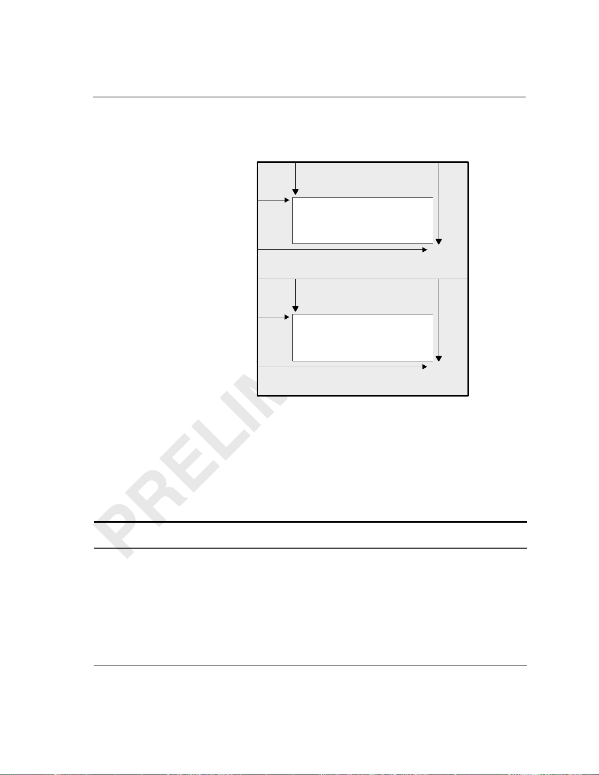
Figure 3–1. Video Capture Parameters
Hcount=0
Ycount=1
BT.656 Video Capture Mode
Ystart
Xstart
Xstop
Ycount=1
Xstart
Xstop
Capture Image
Ystart
Capture Image
Ystop
Field 1
Ystop
Field 2
Table 3–5 shows common digital camera standards and the number of fields
per second, number of active lines per field, and the number of active pixels
per line.
Table 3–5. Common Video Source Parameters
Number of Active Lines
Video Source
square pixel
60Hz/525 lines
BT.601
60 Hz/525 lines
square pixel
50Hz/625 lines
BT.601
50 Hz/625 lines
(Field 1/Field 2)
240/240 640 60
244/243 720 60
288/288 768 50
288/288 720 50
Number of Active Pixels Field Rate (Hz)
3-7Video Capture PortSPRU629
Page 70

BT.656 Video Capture Mode
For the BT.656 video capture mode, the FIFO buffer is divided into three sections (three buffers). One section is 1280 bytes deep and is dedicated for storage of Y data samples. The other two sections are dedicated for storage of Cb
and Cr data samples, respectively . The buffers for Cb and Cr samples are each
640 bytes deep. The incoming video data stream is separated into Y , Cb, and
Cr data streams, scaled (if selected), and the Y, Cb, and Cr buffers are filled.
Each of the three buffers has a memory-mapped location associated with it;
YSRC, CBSRC, and CRSRC. The YSRC, CBSRC, and CRSRC locations are
read only and are used by DMAs to access video data samples stored in the
FIFOs.
If video capture is enabled (BLKCAP bit in VCxCTL is cleared), pixels in the
capture window are captured in the Y, Cb, and Cr buffers. The video capture
module uses the YEVT , CbEVT , and CrEVT events to notify the DMA controller
to copy data from the capture buffers to the DSP memory. The number of
doublewords required to generate the events is set by the VCTHRLDn bits in
VCxTHRLD. On every YEVT, the DMA should move data from the Y buffer to
DSP memory using the YSRC location as the source address. On every
CbEVT, the DMA should move data from the Cb buffer to DSP memory using
the CBSRC location as the source address. On every CrEVT , the DMA should
move data from the Cr buffer to DSP memory using the CRSRC location as
the source address. Note that transfer size from the Cb and Cr buffers is half
of the transfer size from the Y buffer since for every four Y samples, there are
two Cb and two Cr samples.
3.2.4 BT.656 Data Sampling
Incoming data (including timing codes) are sampled and the HCOUNT counter
advanced only on clock cycles for which the CAPEN input is active. Inputs
when CAPEN is inactive are ignored. The timing reference codes are recognized
only when three sequential samples with CAPEN valid are the FFh, 00h, 00h
sequence. A non-00h sample after the FFh or after the first 00h causes the
timing reference recognition logic to be reset and to look for FFh again.
(Unsampled data; those with CAPEN inactive; in the middle of a timing reference
do not cause the recognition logic to be reset since these are not considered
to be valid inputs.)
Video Capture Port3-8 SPRU629
Page 71

3.2.5 BT.656 FIFO Packing
Captured data is always packed into 64-bits before being written into the capture FIFO(s). The packing and byte ordering is dependant upon the capture
data size and the device endian mode. For little-endian operation (default),
data is packed into the FIFO from right to left; for big-endian operation, data
is packed from left to right.
The 8-bit BT.656 mode uses three FIFOs for color separation. Four samples
are packed into each word as shown in Figure 3–2.
Figure 3–2. 8-Bit BT.656 FIFO Packing
VCLKINA / VCLKINB
VDIN[9–2] / VDIN[9–12]
63
Y 31
Y 23
Y 15
Y FIFO
Y 7
Cb 0
5556
Y 30
Y 22
Y 14
Y 6
48 47
Cr 0Y 0
Y 1
40 39
Y 29
Y 21
Y 13
Y 5
Cb 1
Y 28
Y 20
Y 12
Y 4
Y 2
BT.656 Video Capture Mode
Y 3
Cr 1
24
3132
Y 27
23
Y 26
Y 18Y 19
Y 11
Y 3
Y 10
Y 2
Cr 2
Y 4Cb 2
1516
Y 25
Y 17
Y 9
Y 1
Y 5
87 0
Y 24
Y 16
Y 8
Y 0
Cb FIFO
Cr FIFO
Y FIFO
Cb FIFO
Cr FIFO
63
5556
Cb 15
Cb 7
63
5556
Cr 15
Cr 7
Cb 14
Cb 6
Cr 14
Cr 6
48 47
48 47
Cb 13
Cb 5
Cr 13
Cr 5
40 39
3132 24
Cb 12
Cb 4
3940
Cr 12
Cr 4
Cb 11
Cb 3
3132 24
Cr 11
Cr 3
23
1516
Cb 10
Cb 2
23
1516
Cr 10
Cr 2
87
Cb 9
Cb 1
87
Cr 9
Cr 1
0
Cb 8
Cb 0
0
Cr 8
Cr 0
Little-Endian Packing
63
Y 24
Y 16
Y 8
Y 0
63
Cb 8
Cb 0
63
Cr 8
Cr 0
5556
5556
5556
48 47
Y 25
Y 17
Y 9
Y 1
47
48
Cb 9
Cb 1
48 47 40 39
Cr 9
Cr 1
Y 26
Y 18
Y 10
Y 2
Cb 10
Cb 2
Cr 10
Cr 2
40 39
3940
Y 27
Y 19
Y 11
Y 3
Cb 11
Cb 3
Cr 11
Cr 3
3132 24
Y 28
Y 20
Y 12
Y 4
3132 24
Cb 12
Cb 4 Cb 5
3132 24 1516
Cr 12
Cr 4
23
Y 29
Y 21
Y 13
Y 5
23
Cb 13
23
Cr 13
Cr 5
1516
1516
Y 30
Y 22
Y 14
Y 6
Cb 14
Cb 6
Cr 14
Cr 6
87
0
Y 31
Y 23
Y 15
Y 7
87
0
Cb 15
Cb 7
87 0
Cr 15
Cr 7
Big-Endian Packing
3-9Video Capture PortSPRU629
Page 72

BT.656 Video Capture Mode
The 10-bit BT.656 mode uses three FIFOs for color separation. Two samples
are packed into each word with zero or sign extension as shown in Figure 3–3.
Figure 3–3. 10-Bit BT.656 FIFO Packing
VCLKINA / VCLKINB
VDIN[9–0] / VDIN[19–10]
63
58
57
0 / SE
0 / SE
0 / SE
Y FIFO
0 / SE
63
58 57
0 / SE
Cb FIFO
0 / SE
63
58 57
0 / SE
63
0 / SE
58 57
Cr FIFO
0 / SE
0 / SE
0 / SE
63
0 / SE
58 57
Y FIFO
0 / SE
Cb FIFO
0 / SE
Cb 0
Y 15
Y 11
Y 7
Y 3
Cb 7
Cb 3
Cr 7
Cr 3
Y 12
Y 8
Y 4
Y 0
Cb 4
Cb 0
48
48
48
48 47
48 47
47
0 / SE
0 / SE
0 / SE
0 / SE
47
0 / SE
0 / SE
47
0 / SE
0 / SE
0 / SE
0 / SE
0 / SE
0 / SE
0 / SE
0 / SE
Cr 0Y 0
Y 1
4142
4142
4142
Cb 1
Y 14
Y 10
Y 6
Y 2
Cb 6
Cb 2
Cr 6
Cr 2
Y 2
3132 2526
31
3132 2526
313231 2526
0 / SE
0 / SE
0 / SE
0 / SE
0 / SE
0 / SE
0 / SE
0 / SE
Y 3Cr 1
Y 13
Y 9
Y 4
Y 1
Cb 5
Cb 1
Cr 5
Cr 1
Cr 2
Y 4Cb 2
15
16
0 / SE
0 / SE
0 / SE
0 / SE
15
16
0 / SE
0 / SE
15
16
0 / SE
0 / SE
Y 5
10 9 0
Y 12
Y 8
Y 4
Y 0
10 9
Cb 4
Cb 0
910
Cr 4
Cr 0
0
0
Little-Endian Packing
31 2526
42
41
Y 13
Y 9
Y 4
Y 1
42
41
Cb 5
Cb 1
32
0 / SE
0 / SE
0 / SE
0 / SE
32
3131 2526
0 / SE
0 / SE
Y 14
Y 10
Cb 6
Cb 2
Y 6
Y 2
16
16
15
15
0 / SE
0 / SE
0 / SE
0 / SE
0 / SE
0 / SE
10 9
10 9
Y 15
0
Y 11
Y 7
Y 3
0
Cb 7
Cb 3
Cr FIFO
63
0 / SE
0 / SE
58 57
Cr 4
Cr 0
0 / SE
0 / SE
424847 41
Cr 5
Cr 1
32
3131 2526 16
0 / SE
0 / SE
Cr 6
Cr 2
15
0 / SE
0 / SE
910 0
Cr 7
Cr 3
Big-Endian Packing
Video Capture Port3-10 SPRU629
Page 73

The 10-bit BT.656 dense mode uses three FIFOs for color separation. Three
samples are packed into each word with zero extension to provide increased
DMA bandwidth as shown in Figure 3–4.
Figure 3–4. 10-Bit BT.656 Dense FIFO Packing
VCLKINA / VCLKINB
BT.656 Video Capture Mode
VDIN[9–0] / VDIN[19–10]
63
61
Y 23 Y 22
00
Y 17
00
00
Y 11
Y FIFO
Cb FIFO
Cr FIFO
00
63
61
Cb 11
00
Cb 5
00
63
61
Cr 11
00
Cr 5
00
63
61
Y 18
00
Y 12
00
00
Y FIFO
Cb FIFO
Cr FIFO
00
63
61
Cb 6
00
Cb 0
00
63
61
Cr 6
00
Cr 0
00
Y 5
Y 6
Y 0
Cb 0
5152
Y 16
Y 10
Y 4
5152
Cb 10
Cb 4
5152
Cr 10
Cr 4
5152
Y 19
Y 13
Y 7
Y 1
5152
Cb 7
Cb 1
5152 4142
Cr 7
Cr 1
Cr 0Y 0
Y 1
4142
Y 21
Y 15
4142
Cb 9
Cb 3
4142
Cr 9
Cr 3
Cb 1
Y 9
Y 3
Y 2
32 2931
3132 29
00
00
00
00
3132 29
00
00
00
00
Y 3Cr 1
Y 20
Y 14
Y 8
Y 2
Cb 8
Cb 2
Cr 8
Cr 2
Cb 0
20 19
20 19
20
19
Y 4
Cr 2
10 9 0
Y 19
Y 13
Y 7
Y 1
10 9
Cb 7
Cb 1
Cr 7
Cr 1
Y 5
910
Y 18
Y 12
Y 6
Y 0
0
Cb 6
Cb 0
0
Cr 6
Cr 0
Little-Endian Packing
4142
Y 20
Y 14
Y 8
Y 2
4142
Cb 8
Cb 2
Cr 8
Cr 2
293132
Y 21
00
Y 15
00
00
00
3132 29
00
00
3132 29 20 19
00
00
Y 9
Y 3
20 19
Cb 9
Cb 3
Cr 9
Cr 3
1920
Y 22
Y 16
Y 10
Y 4
Cb 10
Cb 4
Cr 10
Cr 4
910
Y 23
Y 17
Y 11
Y 5
10 9
Cb 11
Cb 5
10 9 0
Cr 11
Cr 5
0
0
Big-Endian Packing
3-11Video Capture PortSPRU629
Page 74

Y/C Video Capture Mode
3.3 Y/C Video Capture Mode
The Y/C capture mode is similar to the BT.656 capture mode but captures 8
or 10-bit 4:2:2 data on separate luma and chroma data streams. One data
stream contains Y samples and the other stream contains multiplexed Cb and
Cr samples co-sited with every other Y sample. The Y samples are written into
a Y FIFO and the chroma samples are demultiplexed and written into separate
Cb and Cr FIFOs for transfer into Y, Cb, and Cr buffers in DSP memory. The
packing and order of the samples is determined by the sample size (8-bit or
10-bit) and the device endian mode.
The Y/C capture mode supports HDTV standards such as SMPTE260,
SMPTE296, and BT .1 120 with embedded EAV and SA V codes. It also supports
SDTV YCbCr modes that use separate control signals (sometimes called
CCIR601 mode)
As with the BT .656 capture mode, data bytes where the 8 most-significant bits
are all set to 1 (FF .0h, FF .4h, FF .8h, FF .Ch) or are all cleared to 0 (00.0h, 00.4h,
00.8h, 00.Ch) are reserved for data identification purposes and consequentially only 254 of the possible 256 8-bit words (or 1016 of 1024 10-bit words) may
be used to express signal value.
3.3.1 Y/C Capture Channels
Because Y/C mode requires the entire VDA TA bus, only single channel operation is supported. If the DCHNL bit in VPCTL is set, then Y/C mode cannot be
selected. Y/C capture takes place on channel A only . Both embedded timing
references and external control inputs are supported.
3.3.2 Y/C Timing Reference Codes
Many high-resolution Y/C interface standards provide for embedded timing
reference codes. These codes are identical to those used in the BT.656 standard except that they appear on both the luma (Y) and chroma (CbCr) data
streams in parallel.
Video Capture Port3-12 SPRU629
Page 75

3.3.3 Y/C Image Window and Capture
The SDTV Y/C format (CCIR601) is an interlaced format consisting of two
fields just like BT.656. HDTV Y/C formats may be interlaced or progressive
scan. For interlaced capture, the capture windows are programmed identically
to BT.656 mode. For progressive scan formats, only field1 is used.
In Y/C mode, HCOUNT increments on every luma sample period (every
VCLKINA rising edge) for which capture is enabled. Once YCOUNT = VCYSTART,
line capture begins when HCOUNT = VCXSTART. It continues until
HCOUNT = VCXSTOP. A field’s capture is complete when
HCOUNT = VCXSTOP and VCOUNT = VCYSTOP.
For the Y/C video capture mode, the FIFO buffer is divided into three sections
(three buffers). One section is 2560 bytes deep and is dedicated for storage
of Y data samples. The other two sections are dedicated for storage of Cb and
Cr data samples, respectively. The buffers for Cb and Cr samples are each
1280 bytes deep. The incoming video data stream is separated into Y , Cb, and
Cr data streams, scaled (if selected) and the Y, Cb, and Cr buffers are filled.
Each of the three buffers has a memory-mapped location associated with it;
YSRC, CBSRC, and CRSRC. The YSRC, CBSRC, and CRSRC locations are
read only and are used by DMAs to access video data samples stored in the
FIFOs. Reads must always be 64 bits.
Y/C Video Capture Mode
If video capture is enabled, pixels in the capture window are captured in the
Y, Cb, and Cr buffers. The video capture module uses the YEVT, CbEVT , and
CrEVT events to notify the DMA controller to copy data from the capture buffers to the DSP memory . The number of pixels required to generate the events
is set by the VCTHRLDn bits in VCxTHRLD (the VCTHRLDn value must be an
even number for Y/C mode). The capture module generates the events after
VCTHRLDn new pixels have been received. On every YEVT, the DMA should
move data from the Y buffer to DSP memory using the YSRC register as the
source address. On every CbEVT, the DMA should move data from the Cb
buffer to DSP memory using the CBSRC register as the source address. On
every CrEVT, the DMA should move data from the Cr buffer to DSP memory
using the CRSRC register as the source address. Note that transfer size from
the Cb and Cr buffers is half of the transfer size from the Y buffer since for every
four Y samples, there are two Cb and two Cr samples.
The three DMA events are generated simultaneously when VCTHRLDn is
reached. Each event is reenabled when the first read of the respective FIFO
by the requested DMA begins.
3-13Video Capture PortSPRU629
Page 76

Y/C Video Capture Mode
3.3.4 Y/C FIFO Packing
Captured data is always packed into 64 bits before being written into the
capture FIFO(s). The packing and byte ordering is dependant upon the
capture data size and the device endian mode. For little-endian operation
(default), data is packed into the FIFO from right to left; for big-endian operation, data is packed from left to right.
The 8-bit Y/C mode uses three FIFOs for color separation. Four samples are
packed into each word as shown in Figure 3–5.
Figure 3–5. 8-Bit Y/C FIFO Packing
VCLKINA
Y FIFO
Cb FIFO
Cr FIFO
Y FIFO
Cb FIFO
63
Y 31
Y 15
63
Cb 15
Cb 7
63
Cr 15
63
Y 24
Y 16
63
Cb 8
Cb 0
VDIN[9–2]
VDIN[19–12]
5556
Y 7
5556
5556
Cr 7
5556
Y 8
Y 0
5556
Y 30
Y 22Y 23
Y 14
Y 6
Cb 14
Cb 6
Cr 14
Cr 6
Y 25
Y 17
Y 9
Y 1
Cb 9
Cb 1
Y 0
Cb 0
Y 1
Cr 0
48 47
Y 29
Y 13
Y 5
48 47
Cb 13
Cb 5
4748
Cr 13
Cr 5
4748
Y 26
Y 18
Y 10
Y 2
48 47
Cb 10
Cb 2 Cb 3
Y 2
Cb 1
Cr 1
40
39
39 3231
40
40
39 3231
40
39 3132
39 3231
40
Y 5
Y 4Y 3
Cr 2
Cb 2
32 31
Y 28
Y 20Y 21
Y 12
Y 4
Cb 12
Cb 4
Cr 12
Cr 4
Y 27
Y 19
Y 11
Y 3
Cb 11
Cb 3
Cr 11
Cr 3
Little-Endian Packing
Y 27
Y 19
Y 11
Y 3
Cb 11
Y 28
Y 20
Y 12
Y 4
Cb 12
Cb 4
Y 6
Cb 3
2324
2324
2324
2324
2324
Y 7
Cr 3
Y 26
Y 18
Y 10
Y 2
Cb 10
Cb 2
Cr 10
Cr 2
Y 29
Y 21
Y 13
Y 5
Cb 13
Cb 5
Cb 4
Cb 4
1516
1516
1516
1516
1516
Y 9Y 8
Y 25
Y 17
Y 9
Y 1
Cb 9
Cb 1
Cr 9
Cr 1
Y 30
Y 22
Y 14
Y 6
Cb 14
Cb 6
Y 10
Cb 5
87
87
87
Y 11
Cr 5
78
78
0
Y 24
Y 16
Y 8
Y 0
0
Cb 8
Cb 0
0
Cr 8
Cr 0
0
Y 31
Y 23
Y 15
Y 7
0
Cb 15
Cb 7
Cr FIFO
63 5556
Cr 8
Cr 0
Cr 9
Cr 1
Cr 10
Cr 2
4048 47
39 3231
Cr 11
Cr 3
Cr 12
Cr 4
2324 1516
Cr 13
Cr 5
Cr 14
Cr 6
Cr 15
Big-Endian Packing
Video Capture Port3-14 SPRU629
087
Cr 7
Page 77

The 10-bit Y/C mode uses three FIFOs for color separation. Two samples are
packed into each word with zero or sign extension as shown in Figure 3–6.
Figure 3–6. 10-Bit Y/C FIFO Packing
VCLKINA
Y/C Video Capture Mode
Y FIFO
Cb FIFO
Cr FIFO
Y FIFO
Cb FIFO
Cr FIFO
VDIN[9–0]
VDIN[19–10]
63
0 / SE
0 / SE
0 / SE
0 / SE
63
0 / SE
0 / SE
63
0 / SE
0 / SE
63
0 / SE
0 / SE
0 / SE
0 / SE
63
0 / SE
0 / SE
63
0 / SE
0 / SE
58 57
58 57
58 57
58 57
58 57
58 57
Y 0
Cb 0
Y 15
Y 11
Y 7
Y 3
Cb 7
Cb 3
Cr 7
Cr 3
Y 12
Y 8
Y 4
Y 0
Cb 4
Cb 0
Cr 4
Cr 0
Y 1
Cr 0
48 47
48 47
48 47
48 47
48 47
Y 2
Cb 1
0 / SE
0 / SE
0 / SE
0 / SE
0 / SE
0 / SE
0 / SE
0 / SE
0 / SE
0 / SE
0 / SE
0 / SE
0 / SE
0 / SE
0 / SE
0 / SE
42
42
4248 47 41
Y 4Y 3
Cb 2
Cr 1
4142
Y 14
Y 10
Y 6
Y 2
4142
Cb 6
Cb 2
4142
Cr 6
Cr 2
Little-Endian Packing
41
Y 13
Y 9
Y 4
Y 1
41
Cb 5
Cb 1
Cr 5
Cr 1
Big-Endian Packing
Y 5
Cr 2
3132 2526
0 / SE
0 / SE
0 / SE
0 / SE
313132 2526
0 / SE
0 / SE
313231 2526
0 / SE
0 / SE
31 2526
32
0 / SE
0 / SE
0 / SE
0 / SE
32
3131 2526
0 / SE
0 / SE
32
3131 2526 1516
0 / SE
0 / SE
Y 6
Cb 3
Y 7
Cr 3
Cb 4
Y 13
Y 9
Y 4
Y 1
Cb 5
Cb 1
Cr 5
Cr 1
Y 14
Y 10
Y 6
Y 2
Cb 6
Cb 2
Cr 6
Cr 2
Y 9Y 8
Cr 4
1516
1516
1516
1516
1516
Y 10
Cb 5
0 / SE
0 / SE
0 / SE
0 / SE
0 / SE
0 / SE
0 / SE
0 / SE
0 / SE
0 / SE
0 / SE
0 / SE
0 / SE
0 / SE
0 / SE
0 / SE
Y 11
Cr 5
10 9
Y 12
Y 8
Y 4
Y 0
10 9
Cb 4
Cb 0
910
Cr 4
Cr 0
10 9
Y 15
Y 11
Y 7
Y 3
10 9
Cb 7
Cb 3
910 0
Cr 7
Cr 3
0
0
0
0
0
3-15Video Capture PortSPRU629
Page 78
Y/C Video Capture Mode
The 10-bit Y/C dense mode uses three FIFOs for color separation. Three samples are packed into each word with zero extension to provide increased DMA
bandwidth as shown in Figure 3–7.
Figure 3–7. 10-Bit Y/C Dense FIFO Packing
VCLKINA
Y FIFO
Cb FIFO
Cr FIFO
Y FIFO
Cb FIFO
VDIN[9–0]
VDIN[19–10]
63
61
00
00
00
00
61
63
00
00
61
63
00
00
61
63
00
00
00
00
61
63
00
00
Y 23
Y 17
Y 11
Y 5
Cb 11
Cb 5
Cr 11
Cr 5
Y 18
Y 12
Y 6
Y 0
Cb 6
Cb 0
Y 0
Y 1
Cb 0
Cr 0
5152 4142
Y 22
Y 16
Y 10
Y 4
5152
Cb 10
Cb 4
5152
Cr 10
Cr 4
5152
Y 19
Y 13
Y 7
Y 1
5152
Cb 7
Cb 1
Y 2
Cb 1
Y 4Y 3
Cb 2Cr 1
Y 21
Y 15
Y 9
Y 3
4142
Cb 9
Cb 3
4142
Cr 9
Cr 3
Little-Endian Packing
4142
Y 20
Y 14
Y 8
Y 2
4142
Cb 8
Cb 2
Y 5
Y 6
Cr 2
Cb 3
3132 29
00
00
3132 29
00
00
32 2931
00
00
293132
00
00
00
3132 29
00
00 Cb 3
Y 7
Cr 3
Y 2000
Y 1400
Y 8
Y 2
Cb 8
Cb 2
Cr 8
Cr 2
Y 21
Y 15
Y 900
Y 3
Cb 9
2019
2019
1920
1920
2019
Y 9Y 8
Cr 4Cb 4
Y 19
Y 13
Y 7
Y 1
Cb 7
Cb 1
Cr 7
Cr 1
Y 22
Y 16
Y 10
Y 4
Cb 10
Cb 4
Y 10
Y 11
Cb 5
Cr 5
109 0
109
910
910
109
Cb 11
Y 18
Y 12
Y 6
Y 0
0
Cb 6
Cb 0
0
Cr 6
Cr 0
0
Y 23
Y 17
Y 11
Y 5
0
Cb 5
Cr FIFO
63
00
00
61
Cr 6
Cr 0
5152 4142
Cr 7
Cr 1
Cr 8
Cr 2
Big-Endian Packing
3132 29 2019
00
00
Cr 9
Cr 3
Cr 10
Cr 4
109 0
Cr 11
Cr 5
Video Capture Port3-16 SPRU629
Page 79

BT.656 and Y/C Mode Field and Frame Operation
3.4 BT.656 and Y/C Mode Field and Frame Operation
Because DMAs are used to transfer data from the capture FIFOs to memory ,
there is a large amount of flexibility in the way that capture fields and frames
are transferred and stored in memory. In some cases, for example a DMA
structure can be created to provide a set of ping-pong or round-robin memory
buffers to which a continuous stream of fields are stored without DSP intervention. In other cases, the DSP may need to modify DMA pointer addresses after
each field or frame is captured. In some applications, only one field may be
captured and the other ignored completely , or a frame may need to be ignored
in order to have time to process a previous frame. The video port addresses
these issues by providing programmable control over different aspects of the
capture process.
3.4.1 Capture Determination and Notification
The video port treats the capture of every field as a separate operation. In order
to accommodate various capture scenarios, DMA structures, and processing
flows, the video port employs a flexible capture and DSP notification method.
This is programmed using the CON, FRAME, CF1, and CF2 bits in VCxCTL.
The CON bit controls the capture of multiple fields or frames. When CON = 1,
continuous capture is enabled, the video port captures incoming fields
(assuming the VCEN bit is set) without the need for DSP interaction. It relies
on a DMA structure with circular buffering capability to service the capture
FIFOs. When CON = 0, continuous capture is disabled, the video port sets a
field or frame capture complete bit (F1C, F2C, or FRMC) in VCxST AT upon the
capture of each field as determined by the state of the other capture control
bits (FRAME, CF1, and CF2). Once the capture complete bit is set, at most,
one more field or frame can be received before capture operation is halted.
This prevents subsequent data from overwriting previous fields until the DSP
has a chance to update DMA pointers or process those fields. When a capture
halt occurs, the video port stops capturing data (for the halted field). It then
checks the appropriate capture complete bit at the start of each subsequent
field and resumes capture if the bit has been cleared.
The CON, FRAME, CF1, and CF2 bits encode the capture operations as listed
in Table 3–6.
3-17Video Capture PortSPRU629
Page 80

BT.656 and Y/C Mode Field and Frame Operation
Table 3–6. BT.656 and Y/C Mode Capture Operation
VCxCTL Bit
CON FRAME CF2 CF1 Operation
0
0 0 0 1 Noncontinuous field 1 capture. Capture only field 1. F1C is set after
0 0 1 0 Noncontinuous field 2 capture. Capture only field 2. F2C is set after
0 0 1 1 Noncontinuous field 1 and field 2 capture. Capture both fields. F1C is
0 1 0 0 Noncontinuous frame capture. Capture both fields. FRMC is set after
0 0 0 Reserved
field 1 capture and causes CCMPx to be set. The F1C bit must be
cleared by the DSP before capture can continue. (The DSP has the
entire field 2 time to clear F1C before next field 1 begins.) Can also be
used for single progressive frame capture. (The DSP has vertical
blanking time to clear F1C before next frame begins.)
field 2 capture and causes CCMPx to be set. The F2C bit must be
cleared by the DSP before capture can continue. (The DSP has the
entire field 1 time to clear F2C before next field 2 begins.)
set after field 1 capture and causes CCMPx to be set. The F1C bit must
be cleared by the DSP before another field 1 capture can occur. (The
DSP has the entire field 2 time to clear F1C before next field 1 begins.)
F2C is set after field 2 capture and causes CCMPx to be set. The F2C
bit must be cleared by the DSP before another field 2 capture can
occur. (The DSP has the entire field 1 time to clear F2C before next
field 2 begins.)
field 2 capture and causes CCMPx to be set. Capture halts upon
completion of the next frame unless the FRMC bit is cleared. (The DSP
has the entire next frame time to clear FRMC.)
0 1 0 1 Noncontinuous progressive frame capture. Capture field 1. FRMC is set
after field 1 capture and causes CCMPx to be set. Capture halts upon
completion of the next frame unless the FRMC bit is cleared. (The DSP
has the entire next frame time to clear FRMC.)
0 1 1 0 Reserved
0 1 1 1 Single frame capture. Capture both fields. FRMC is set after field 2
capture and causes CCMPx to be set. Capture halts until the FRMC bit
is cleared. (The DSP has the field 2 to field 1 vertical blanking time to
clear FRMC.)
1 0 0 0 Reserved
1
0 0 1 Continuous field 1 capture. Capture only field 1. F1C is set after field 1
capture and causes CCMPx to be set (CCMPx interrupt can be
disabled). The video port continues capturing field 1 fields, regardless
of the state of F1C.
Video Capture Port3-18 SPRU629
Page 81

BT.656 and Y/C Mode Field and Frame Operation
Table 3–6. BT.656 and Y/C Mode Capture Operation (Continued)
VCxCTL Bit
CON OperationCF1CF2FRAME
1 0 1 0 Continuous field 2 capture. Capture only field 2. F2C is set after field 2
capture and causes CCMPx to be set (CCMPx interrupt can be
disabled). The video port continues capturing field 2 fields, regardless
of the state of F2C.
1 0 1 1 Reserved
1 1 0 0 Continuous frame capture. Capture both fields. FRMC is set after
field 2 capture and causes CCMPx to be set (CCMPx interrupt can be
disabled). The video port continues capturing frames, regardless of the
state of FRMC.
1 1 0 1 Continuous progressive frame capture. Capture field 1. FRMC is set
after field 1 capture and causes CCMPx to be set (CCMPx interrupt can
be disabled). The video port continues capturing frames, regardless of
the state of FRMC. (Functions identically to continuous field 1 capture
mode except the FRMC bit is used instead of the F1C bit.)
1 1 1 0 Reserved
1
1 1 1 Reserved
3.4.2 Vertical Synchronization
The video port uses a capture window to determine which incoming data samples
to capture in each field. The capture module uses a vertical line counter
(VCOUNT) to track which video line is currently being received. The line counter is compared to the appropriate capture window start (VCYSTART1 or
VCYSTART2) and stop (VCYSTOP1 or VCYSTOP2) values for the current
field to determine if the current line is within the capture window. In order to
correctly align the capture window within the field, the capture module must
know which line should correspond to the first line of the field, that is, when to
reset the line counter. This point may vary depending on the type of capture
being performed and the signals available for vertical synchronization. The
video port allows the vertical counter reset trigger to be determined by
programming the EXC and VRST bits in VCxCTL. The encoding of these bits
is shown in Table 3–7. Note that VModes 2 and 3 are only available for single
channel operation (channel A).
3-19Video Capture PortSPRU629
Page 82

BT.656 and Y/C Mode Field and Frame Operation
Table 3–7. Vertical Synchronization Programming
VCxCTL Bit
VMode EXC VRST Vertical Counter Reset Point
0
1 0 1 First EAV with V=0 after EAV with V=1 – first active line. VCOUNT
2 1 0 On HCOUNT reset after VCTL2 input active edge – beginning of vertical
3
0 0 First EAV with V=1 after EAV with V=0 – beginning of vertical blanking period.
VCOUNT increments on each EAV.
increments on each EA V.
blanking or vertical sync period. (VCTL2 must be configured as vertical
control signal). VCOUNT increments when HCOUNT is reset.
1 1 On HCOUNT reset after VCTL2 input inactive edge – end of vertical sync or
first active scan line. (VCTL2 must be configured as vertical control signal).
VCOUNT increments when HCOUNT is reset.
VMode 0 is used for BT .656 or Y/C capture (with embedded control) and corresponds to most digital video standards that number lines beginning with the
start of vertical blanking. VMode 1 can also be used for BT .656 or Y/C capture
but counts from the first active video line. This makes field detection more
straightforward in some instances (see section 3.4.4) and allows the
VCYSTARTn bit to be set to 1, but also has the effect of associating vertical
blanking periods with the end of the previous field rather than the beginning
of the current field. (This could be an issue when capturing VBI data.)
VCOUNT operation for VMode 0 and VMode 1 is shown in Figure 3–8.
VMode 2 and VMode 3 are used for BT.656 or Y/C capture without embedded
EA V/SAV codes and allow alignment with either the active or inactive edge of
the vertical control signal on VCTL2. This can be a VBLNK or VSYNC signal
from the video decoder.
Video Capture Port3-20 SPRU629
Page 83
BT.656 and Y/C Mode Field and Frame Operation
Figure 3–8. VCOUNT Operation Example (EXC = 0)
VRST=0
VF
10 525
11
11
11
01
01
01
00
00
Line
19
20
21
VCOUNT
262
1
2
3
4
5
Field 1 Blanking
1
2
3
4
5
19
20
21
Field 1 Active
FINV=0 FINV=1
Field
1
2
Field
2
1
VCOUNT
243 2
244
245
246
247
248
262
1
2
VRST=1
FINV=0 FINV=1
Field
2
1
Field
1
1
2
26300
26401
26501
26611
26711
28211
28310
28410
Field 2 Blanking
263
1
2
3
4
19
20
21
2
1
1
2
244
245
246
247
248
263
1
2
12
21
Field 2 Active
52410
52510
111
261
262
1
1
2
2
1
242
243
244
21
3-21Video Capture PortSPRU629
Page 84

BT.656 and Y/C Mode Field and Frame Operation
3.4.3 Horizontal Synchronization
Horizontal synchronization determines when the horizontal pixel/sample
counter is reset. The EXC and HRST bits in VCxCTL allow you to program the
event that triggers the start of a line. The encoding of these bits is shown in
Table 3–8.
Table 3–8. Horizontal Synchronization Programming
VCxCTL Bit
HMode EXC HRST Horizontal Counter Reset Point
0
1 0 1 SAV code (H=0) – Start of active video.
2 1 0 VCTL1 input active edge – beginning of horizontal blanking or horizontal
3
0 0 EAV code (H=1) – beginning of horizontal blanking.
sync period. (VCTL1 must be configured as a horizontal control signal.)
1 1 VCTL1 input inactive edge – first active pixel on line or end of horizontal
sync. (VCTL1 must be configured as a horizontal control signal.)
HMode 0 is used for BT .656 or Y/C capture (with embedded control) and corresponds to the idea that each line begins with the horizontal blanking period.
It does not align with most standards that start counting with the first active pixel;
therefore, is only useful if capturing of HANC data before the SAV code is
desired. HMode 1 is the default mode and corresponds to most digital video
standards by making the first active pixel pixel0. It has the effect of associating
horizontal blanking periods with the end of the previous line rather than the
beginning of the line, but this is only an issue if you try to capture HANC data.
In either mode, HCOUNT increments on every VCLKIN edge for Y/C operation
and on every other VCLKIN edge for BT .656 operation but only when CAPEN
is active. HCOUNT operation for HMode 0 and HMode 1 is shown in
Figure 3–9.
HMode 2 and HMode 3 are used for BT .656 or Y/C capture without embedded
EA V/SA V code and allow alignment with either the beginning of the horizontal
blanking period or the first active pixel, or the beginning or end of horizontal
sync depending on the VCTL1 input. When VCTL1 is configured as a horizontal
control input, no external CAPEN signal is available so the CAPEN signal is
considered to always be active. HCOUNT operation for HMode 3 and
HMode 4 is shown in Figure 3–10 for VCTL1 operating as either HSYNC or
AVID.
Video Capture Port3-22 SPRU629
Page 85

BT.656 and Y/C Mode Field and Frame Operation
Figure 3–9. HCOUNT Operation Example (EXC = 0)
VCLKIN
4
268 1440
4
Active VideoBlanking
VDIN[9–0]
FF.C
00.0
00.0
80.0
80.0
10.0
10.0
XY.0
80.0
10.0
00.0
FF.C
00.0
Y 0
XY.0
Cb 0
SAVEAV Blanking Data EAV
EXC=0
HRST=0
EXC=0
HRST=1
HCOUNT
HCOUNT
720 721 722 723
856 857 0 1
One Line
855 856 857 0 1 2
One Line
133 134 135 136 273 274
VCOUNT
Figure 3–10. HCOUNT Operation Example (EXC = 1)
VCLKIN
276
Blanking
VDIN[9–0]
80.0
Blanking Data
10.0
80.0
10.0
80.0
10.0
80.0
10.0
10.0
80.0
10.0
80.0
80.0
10.0
80.0
Cr 0
n n+1n–1
10.0
Y 1
80.0
Cb 1
10.0
Y 2
Cb 0
Y 0
Active Video
Y 1
Cr 0
Cb 1
Y 718
Y 719
Cr 359
Cb 359
718 719 720 721 722 723
854 855 856 857 0 1
1440
Y 2
Cb 0
Y 718
Next Line
Next Line
80.0
Y 719
Cr 359
10.0
80.0
10.0
80.0
10.0
EXC=1
HRST=0
EXC=1
HRST=1
EXC=1
HRST=0
EXC=1
HRST=1
HSYNC
HCOUNT
VCOUNT
HCOUNT
VCOUNT
AVID
HCOUNT
VCOUNT
HCOUNT
VCOUNT
842
778
720
n
5857 59
138137 139
124
60
140
843
842842840
844
779
777776 778
n
2
n
857856 0
780
721
720719718
722
1
2
n+1
843
n–1
779
780
721
1
0
2
n–1
857844
793
735722
15
0
794
736
16
n–1
63
857
799
79
80 135
0 55
n
12011964
56
856855800
136
121 123122
857 10
3-23Video Capture PortSPRU629
Page 86

BT.656 and Y/C Mode Field and Frame Operation
3.4.4 Field Identification
In order to properly synchronize to the source data stream and capture the
correct fields, field identification needs to be performed. Field identification is
made using one of three methods: EAV, field indicator input, or field detect
logic. The field identification method is determined by the EXC, FLDD, and
FINV bits in VCxCTL.
Table 3–9. Field Identification Programming
VCxCTL Bit
EXC FLDD Field Detect Method
0
0 1 EAV code
1 0 Use FID input
1
0 EAV code
1 Use field detect (from HSYNC and VSYNC inputs)
In the BT .656 standard and in many Y/C standards, a field identification (F) bit
is contained in EA V and SA V codes embedded in the data stream. In the EAV
field detect method, the F bit in the EA V of the first line of every field is checked.
If F = 0, then the current field is defined as field 1. If F = 1, then the current field
is defined as field 2. Depending on how the first line of a field is defined (as
determined by the VRST bit in VCxCTL) and the video stream being captured,
the F value at the start of a field may not reflect the actual field being supplied.
The FINV bit in VCxCTL allows the detected field value to be inverted. (For
example, in BT.656 525/60 operation, the F bit changes to 0 to indicate field 1
on the fourth line of the field. If the VRST bit is cleared so the line counter begins
counting at line 1 of the field (the first EA V where V is 1), then the F bit still indicates field 2 (F = 1) and needs to be inverted. If the VRST bit is set to start
counting lines beginning with the first active line (the first EAV where V is 0),
the F value will have already changed to indicate field 1 (F = 0) and no inversion is necessary.)
The field indicator method uses the FID input directly to determine the current
field. This is useful for Y/C data streams that do not have embedded EA V and
SA V codes. The FID input is sampled at the start of each field. If FID = 0, then
field 1 is starting; if FID = 1, then field 2 is starting. The start of each field is
defined by the VRST bit in VCxCTL and is either the start or end of vertical
blanking as determined by the VBLNK input. The FINV bit may be used in this
method in systems where the FID input has the opposite polarity or where the
field identification change lags the start of the field.
Video Capture Port3-24 SPRU629
Page 87

The field detect method uses HYSNC and VSYNC based field detect logic.
This is used for BT .656 or Y/C systems that provide only HSYNC and VSYNC.
The field detect logic samples the state of the HSYNC input on the VSYNC
active edge. If HSYNC is active on the active VSYNC edge, then field 1 is
detected; if HSYNC is inactive on the active VSYNC edge, then field 2 is detected. Because of slight timing variations, the VSYNC transition may not coincide
exactly with the HSYNC transition. The detection logic should implement a
±64 clock detection window around HSYNC. If both HSYNC and VSYNC
leading edges occur within 64 cycles of each other, then field 1 is detected;
otherwise, field 2 is assumed. This is shown in Figure 3–1 1 for active-low sync
signals.
Figure 3–11.Field 1 Detection Timing
VCLKIN
VSYNC#
(VCTL2)
HSYNC#
(VCTL1)
64 Clocks
BT.656 and Y/C Mode Field and Frame Operation
64 Clocks
3.4.5 Short and Long Field Detect
The short and long field detect logic is used to notify the DSP when a captured
field shorter or longer than expected. Detection is enabled by the SFDE and
LFDE bits in VCxCTL. The SFD and LFD bits in VPIS indicate when a short
or long field occurred and trigger an interrupt to the DSP if enabled.
If a vertical blanking period is detected before the end of the capture field, a
short field is detected . If EAV is used for vertical sync (EXC = 0), then a short
field is detected when an EAV with V = 1 occurs on or before
VCOUNT = VCYSTOPn. If the VCTL2 input is used for vertical sync
(EXC = 1), then a short field is detected if a VCTL2 active edge occurs before
VCOUNT = VCYSTOPn.
If a vertical blanking period occurs more than 1 line past the end of the capture
field, a long field is detected. A long field is detected when
VCOUNT = VCYSTOPn + 1. (A long field is only detected when the VRST bit
in VCxCTL is cleared to 0; when VRST = 1, a long field is always detected.)
Long field detection cannot be used if the capture window is a vertical subset
of the field that crops lines at the bottom. Such a window would always result
in a long field detection. If VCTL2 is used for vertical sync, then the VCTL2 signal must represent VBLNK (vertical blank) for proper long field detect. If
3-25Video Capture PortSPRU629
Page 88

Video Input Filtering
VCTL2 is a VSYNC (vertical sync) input, then a long field is always detected.
(Even if VCYSTOPn is set to the last active line, VCOUNT usually increments
past VCYSTOPn + 1 while it counts the vertical front porch lines that occur
prior to VSYNC active.)
3.5 Video Input Filtering
The video input filter performs simple hardware scaling and resampling on
incoming 8-bit BT .656 or 8-bit Y/C data. Filtering hardware is always disabled
during 10-bit or raw data capture modes. For proper filter operation, the
channel’s EXC bit in VCxCTL must be cleared to 0 (embedded timing reference codes used) and the CAPEN input must not go inactive during the active
video window.
3.5.1 Input Filter Modes
The input filter has four modes of operation: no-filtering, ½ scaling, chrominance
resampling, and ½ scaling with chrominance resampling. Filter operation is
determined by the CMODE, SCALE, and RESMPL bits of VCxCTL.
Table 3–10 shows the input filter mode selection. When 8-bit BT.656 or Y/C
capture operation is selected (CMODE = x00), scaling is selected by setting
the SCALE bit and chrominance resampling is selected by setting the
RESMPL bit. If 8-bit BT.656 or Y/C capture is not selected (CMODE ≠ x00),
filtering is disabled.
Table 3–10. Input Filter Mode Selection
VCxCTL Bit
CMODE RESMPL SCALE Filter Operation
x00
x00 0 1 ½ scaling
x00 1 0 Chrominance resampling (full scale)
x00 1 1 ½ scaling with chrominance resampling
x01 x x No filtering
x10 x x No filtering
x11
0 0 No filtering
x x No filtering
Video Capture Port3-26 SPRU629
Page 89

3.5.2 Chrominance Resampling Operation
Chrominance resampling computes chrominance values at sample points
midway between the input luminance samples based on the input co-sited
chrominance samples. This filter performs the horizontal portion of a conversion between YCbCr 4:2:2 format and YCbCr 4:2:0 format. The vertical portion
of the conversion must be performed in software.
The chrominance resampling filters calculate the implied value of Cb and Cr
in between luminance sample points based upon nearby co-sited Cb and Cr
samples. The resulting values are clamped to between 01h and FEh and sent
to the Cb and Cr capture buffers. Chrominance resampling is shown in
Figure 3–12.
Figure 3–12. Chrominance Resampling
Video Input Filtering
abc d e f g h i j k
YCbCr 4:2:2 co-sited
input samples
chroma-resampled
capture results
Luma (Y)
–
sample
3.5.3 Scaling Operation
The ½-scaling mode is used to reduce the horizontal resolution of captured
luminance and chrominance data by a factor of two. For applications that
require only CIF or lower resolutions, this reduces the video capture buffer
memory requirements (and the bandwidth needed to write the buffer) by a
factor of two. Vertical scaling must be performed in software. (The bandwidth
to load in the buffer is again reduced by 50% over the nonhorizontal scaled
case.)
The filtering for the luminance portion of the scaling filter changes depending
on if chrominance resampling is also enabled. (By changing the luminance filter,
the chrominance filters can remain the same.) The resulting values are
clamped to between 01h and FEh and sent to the Y , Cb, and Cr capture buffers.
Scaling for co-sited capture is shown in Figure 3–13 and scaling for chrominance resampling is shown in Figure 3–14.
Chroma (Cb/Cr)
samples
l
Cb’ef = (–3Cbc+ 101Cbe+ 33Cbg–3Cbi ) / 128
Cr’ef = (–3Crc+ 101Cre+ 33Crg– 3Cri) / 128
3-27Video Capture PortSPRU629
Page 90

Video Input Filtering
Figure 3–13. 1/2 Scaled Co-Sited Filtering
YCbCr 4:2:2 co-sited
input samples
1/2 scaled co-sited
capture results
Luma (Y)
–
sample
abcde fgh i jk l
Chroma (Cb/Cr)
–
samples
Y’f = (–3Yc+ 32Ye+ 70Yf+ 32Yg – 3Yi) / 128
Cb’
= (–1Cbc+ 17Cbe+ 17Cbg – 1Cbi ) / 32
f
Cr’f = (–1Crc+ 17Cre+ 17Crg – 1Cri ) / 32
Y’h = (–3Ye+ 32Yg+ 70Yh+ 32Yi – 3Yk) / 128
Figure 3–14. 1/2 Scaled Chrominance Resampled Filtering
YCbCr 4:2:2 co-sited
input samples
chroma-resampled
1/2 scaled
capture results
Luma (Y)
–
sample
abcde fghi
Chroma (Cb/Cr)
–
samples
Y’g = (–3Yd + 32Yf + 70Yg + 32Yh –3Yj) / 128
Cb’f = (–1Cbc + 17Cbe + 17Cbg – 1Cbi) / 32
Cr’
= (–1Crc + 17Cre + 17Crg – 1Cri ) / 32
f
j
kl
Note that because input scaling is limited to ½, true CIF horizontal resolution
is not achieved if the full BT.656 horizontal line (720 pixels) is captured. A CIF
size line can be captured by selecting a 704 pixel-sized window within the
BT.656 line. This window size and location on the line are programmed using
the VCXST ARTn and VCXSTOPn bits.
Note that when ½ scaling is selected, horizontal timing applies to the incoming
data (before scaling). The VCTHRLD value applies to the data written into the
FIFO after scaling.
Video Capture Port3-28 SPRU629
Page 91

3.5.4 Edge Pixel Replication
Because the filters make use of preceding and trailing samples, filtering artifacts can occur at the beginning of the BT.656 or Y/C active line because no
samples exist before the SAV code, and at the end of the BT.656 active line
because no samples exist after the EAV code. In order to minimize artifacts,
the first m samples after sample 0 (where m is the maximum number of
preceding samples used by any of the filters) are mirrored to the left of
sample 0 and the last m samples before the last sample are mirrored to the
right of the last sample.
Figure 3–15 shows edge pixel replication assuming an m value of 3. Sample a
is the first sample after the SA V code. Therefore, samples b–d are mirrored to
the left of sample a to provide values for the filter calculations on the first few
pixels in the line. Likewise, samples n – 1 to n – 3 are mirrored to the right of
the last sample n to provide values for the last few pixels on the line.
Note that edge pixel replication only comes into effect when the full BT.656
stream is being captured. If VCXSTART is greater than 0, then only some of
the leading edge replicated pixels are used by the filter. If VCXST ART is greater
than m, then none of the leading edge replicated pixels are used. Similarly, if
VCXSTOP is less than the number of samples before EAV, then none or only
some of the trailing edge replicated pixels are used by the filters.
Video Input Filtering
Figure 3–15. Edge Pixel Replication
abcdeSAV n – 1 n EAVn – 4n – 3n – 2
a
b c d ed c bn – 1nn – 1n – 2n – 3n – 4n – 3n – 2
Leading edge replicated pixels
Luma (Y)
–
sample
Active line
Chroma (Cb/Cr)
–
samples
Trailing edge replicated pixels
3-29Video Capture PortSPRU629
Page 92

Video Input Filtering
Figure 3–16 shows an example of a capture window that is smaller than the
BT.656 active line. Sample a is the first sample in the horizontal capture
window and sample n is the last sample. In this case, any filtering done on the
first sample location uses the m leading edge captured pixels (m is 3 in this
example), and any filtering done on the last sample location uses the m trailing
captured pixels. (From an implementation standpoint, the mirroring and filtering can still begin and end with SAV and EAV, but the samples before
VCXSTART or after VCXSTOP must not be saved to the YCbCr buffers.)
Figure 3–16. Capture Window Not Requiring Edge Pixel Replication
XSTART
XSIZE
a–4a–3 de n+4n+1 n+2 n+3
a–2a–1a b cSAV n–1 n EAVn–4n–3n–2
Active line
a
b c d ea–4 a–3 a–1n–1 n n+1 n+2 n+3n–4n–3n–2
Leading edge replicated pixels
Luma (Y)
–
sample
Trailing edge replicated pixels
Chroma (Cb/Cr)
–
samples
Video Capture Port3-30 SPRU629
Page 93

3.6 Ancillary Data Capture
The BT .656 and some Y/C specifications includes provision for carrying ancillary
(nonvideo) data within the horizontal and vertical blanking regions. Horizontal
ancillary (HANC) data appears between the EA V code and SAV codes. V ertical
ancillary (V ANC) data, also called vertical blanking interval (VBI) data, appears
during the active horizontal line portion of vertically blanking (for example, after
an SAV with V = 1).
3.6.1 Horizontal Ancillary (HANC) Data Capture
No special provisions are made for the capture of HANC data. HANC data may
be captured using the normal video capture mechanism by programming
VCXSTRT to occur before the SA V (when HCOUNT is reset by the EA V code)
or by programming VCXSTOP to occur past the EAV code (when HCOUNT
is reset by the SA V code). Note that the EA V code and any subsequent HANC
data will still be YCbCr separated. Software must parse the Y, Cb, and Cr
memory buffers to determine any HANC data presence and to reconstruct the
HANC data. The VCTHRLD value and DMA size must be programmed to
comprehend the additional samples. Y ou must disable scaling and chroma resampling when including the capture of HANC data to prevent data corruption.
Ancillary Data Capture
3.6.2 Vertical Ancillary (VANC) Data Capture
V ANC (or VBI) data is commonly used for such features as teletext and closedcaptioning. No special provisions are made for the capture of VBI data. VBI
data may be captured using the normal capture mechanism by programming
VCYSTART to occur before the first line of active video on the first line of
desired VBI data. (VCOUNT must be reset by an EAV with V = 1). Note that
the VBI data will be YCbCr separated. Software must parse the Y, Cb, and Cr
memory buffers to determine any VBI data presence and to reconstruct the
VBI data. Y ou must disable scaling and chroma resampling when the capture
of VBI data is desired or the data will be corrupted by the filters.
3-31Video Capture PortSPRU629
Page 94

Raw Data Capture Mode
3.7 Raw Data Capture Mode
In the raw data capture mode, the data is sampled by the interface only when
the CAPEN signal is active. Data is captured at the rate of the sender’s clock,
without any interpretation or start/stop of capture based on the data values.
To ensure initial capture synchronization to the beginning of a frame, an
optional setup synchronization enable (SSE) bit is provided in VCxSTRT1. If
the SSE bit is set, then when the VCEN bit is set to 1, the video port will not
start capturing data until after detecting two vertical blanking intervals. If the
SSE bit is cleared to 0, capture begins immediately when the VCEN bit is set.
The incoming digital video capture data is stored in the FIFO, which is 2560-bytes
(in dual-channel operation) or 5120-bytes deep (in single-channel operation).
The memory-mapped location YSRCx is associated with the Y buffer. The
YSRCx location is a read-only register and is used to access video data
samples stored in the buffer.
The captured data set size is set by VCxSTOPn. The VCXSTOP and VCYSTOP
bits set the 24-bits of data set size (VCXSTOP sets the lower 12 bits and
VCYSTOP sets the upper 12 bits). Capture is complete and the appropriate
F1C, F2C, or FRMC bit is set when the captured data size reaches the
combined VCYSTOP and VCXSTOP value.
The video port generates a YEVT after the specified number of new samples
has been captured in the buffer . The number of samples required to generate
YEVTx is programmable and is set in the VCTHRLDn bits of VCxTHRLD. On
every YEVT, the DMA should move data from the buffer to the DSP memory.
When moving data from the buffer to the DSP memory, the DMA should use
the YSRCx location as a source address.
3.7.1 Raw Data Capture Notification
Raw data mode captures a single data packet of information using only
CAPEN for control. Field information is available only for channel A operation
using the FID input on VCTL3. If the RDFE bit in VCACTL is set, then the video
port samples the FID input at the start of each data block (when DCOUNT = 0
and CAPENA is active) to determine the current field. In this case, the CON,
FRAME, CF1, and CF2 bits in VCxCTL are used in a manner identical to
BT.656 mode (see section 3.4.1).
For channel B operation or when the RDFE bit in VCACTL is not set, no field
information is available. Some flexibility in capture and DSP notification is still
provided in order to accommodate various DMA structures and processing
flows. Each raw data packet is treated similar to a progressive scan video
frame. The raw data mode uses the CON and FRAME bits of VCxCTL in a
slightly different manner, as listed in Table 3–11.
Video Capture Port3-32 SPRU629
Page 95

Table 3–11. Raw Data Mode Capture Operation
VCxCTL Bit
CON FRAME CF2 CF1 Operation
Raw Data Capture Mode
0
0 1 x x Single frame capture. FRMC is set after data block capture and causes
1 0 x x Continuous frame capture. FRMC is set after data block capture and
1
0 x x Noncontinuous frame capture. FRMC is set after data block capture
and causes CCMPx to be set. Capture will halt upon completion of the
next frame unless the FRMC bit is cleared. (DSP has the entire next
frame time to clear FRMC.)
CCMPx to be set. Capture is halted until the FRMC bit is cleared.
causes CCMPx to be set (CCMPx interrupt can be disabled). The port
will continue capturing frames regardless of the state of FRMC.
1 x x Reserved
The CON bit controls the capture of multiple frames. When CON = 1, continuous
capture is enabled, the video port captures incoming frames (assuming the
VCEN bit is set) without the need for DSP interaction. It relies on a DMA
structure with circular buffering capability to service the capture FIFO. When
CON = 0, continuous capture is disabled, the video port sets the frame capture
complete bit (FRMC) in VCxSTAT upon the capture of each frame. Once the
capture complete bit is set, at most, one more frame can be received before
capture operation is halted (as determined by the FRAME bit state). This
prevents subsequent data from overwriting previous frames until the DSP has
a chance to update DMA pointers or process those frames.
3.7.2 Raw Data FIFO Packing
Captured data is always packed into 64-bits before being written into the
capture FIFO(s). The packing and byte ordering is dependant upon the
capture data size and the device endian mode. For little-endian operation
(default), data is packed into the FIFO from right to left; for big-endian operation, data is packed from left to right.
3-33Video Capture PortSPRU629
Page 96

Raw Data Capture Mode
The 8-bit raw-data mode stores all data in a single FIFO. Four samples are
packed into each word as shown in Figure 3–17.
Figure 3–17. 8-Bit Raw Data FIFO Packing
VCLKINA / VCLKINB
VDIN[9–2] / VDIN[19–12]
63 5655 4847 4039 32
Raw FIFO
63 5655 4847 4039 32
Raw FIFO
Raw 9Raw 8 Raw 11Raw 10
Raw 1Raw 0 Raw 3Raw 2
Raw 2 Raw 4 Raw 6Raw 1 Raw 3 Raw 5 Raw 7
Raw 13 Raw 12Raw 15 Raw 14
Raw 5 Raw 4Raw 7 Raw 6
Little-Endian Packing
Big-Endian Packing
The 10-bit raw data mode stores all data into a single FIFO. Two samples are
packed into each word with zero or sign extension as shown in Figure 3–18.
Figure 3–18. 10-Bit Raw Data FIFO Packing
VCLKINA / VCLKINB
VDIN[9–0] / VDIN[19–10]
Raw 0 Raw 2 Raw 4 Raw 6Raw 1 Raw 3 Raw 5 Raw 7 Raw 8 Raw 10Raw 9 Raw 11
Raw 8 Raw 10Raw 9 Raw 11Raw 0
31 2423 1615 8 7 0
Raw 9 Raw 8Raw 11 Raw 10
Raw 1 Raw 0Raw 3 Raw 2
31 2423 1615 8 7 0
Raw 13Raw 12 Raw 15Raw 14
Raw 5Raw 4 Raw 7Raw 6
Y FIFO
Y FIFO
63 58 57 48 47 42 41 32
0 / SE Raw 14
0 / SE Raw 10
0 / SE Raw 6
0 / SE Raw 2
63 58 57 48 47 42 41 32
0 / SE Raw 14
0 / SE Raw 10
0 / SE Raw 6
0 / SE Raw 2
0 / SERaw 15
0 / SERaw 11
0 / SERaw 7
0 / SERaw 3
Little-Endian Packing
0 / SE Raw 15
0 / SE Raw 11
0 / SE Raw 7
0 / SE Raw 3
Big-Endian Packing
31 26 25 16 15 10 9 0
0 / SE Raw 12
0 / SE Raw 8
0 / SE Raw 4
0 / SE Raw 0
31 26 25 16 15 10 9 0
0 / SERaw 12
0 / SERaw 8
0 / SERaw 4
0 / SERaw 0
0 / SERaw 13
0 / SERaw 9
0 / SERaw 5
0 / SERaw 1
0 / SERaw 13
0 / SERaw 9
0 / SERaw 5
0 / SERaw 1
Video Capture Port3-34 SPRU629
Page 97

The 10-bit dense raw data mode stores all data into a single FIFO. Three samples are packed into each word with zero extension as shown in Figure 3–19.
Figure 3–19. 10-Bit Dense Raw Data FIFO Packing
VCLKOUT
Raw Data Capture Mode
Raw 0 Raw 2 Raw 4 Raw 6Raw 1 Raw 3 Raw 5 Raw 7 Raw 8 Raw 10Raw 9 Raw 11
Raw 5
Raw 12
Raw 6
Raw 0
Raw 16
Raw 10
Raw 4
Raw 13
Raw 7
Raw 1
Raw 15
Raw 9
Raw 3
Little-Endian Unpacking
Raw 14
Raw 8
Raw 2
Big-Endian Unpacking
Y FIFO
Y FIFO
VDOUT[9–0]
63 61 5251 4241
00
Raw 17
00
Raw 11
00
63 61 5251 4241
00
00
00
The 16-bit raw data mode stores all data into a single FIFO. Two samples are
packed into each word as shown in Figure 3–20.
Figure 3–20. 16-Bit Raw Data FIFO Packing
32
31 29 2019 109 0
00
Raw 14
00
Raw 8
00
Raw 2
32
31 29 2019 10 9 0
00
Raw 15
00
00
Raw 9
Raw 3
Raw 13
Raw 7
Raw 1
Raw 16
Raw 10
Raw 4
Raw 12
Raw 6
Raw 0
Raw 17
Raw 11
Raw 5
VDIN[19–12] / VDIN[9–2]
63 4847 32
Raw FIFO
63 4847 32
Raw FIFO
VCLKINA
Raw 2 Raw 4 Raw 6Raw 1 Raw 3 Raw 5 Raw 7
Raw 10Raw 11 Raw 8Raw 9
Raw 6Raw 7
Raw 2Raw 3
Raw 4 Raw 5
Raw 0 Raw 1
Raw 8 Raw 10Raw 9 Raw 11Raw 0
31 1615 0
Raw 4Raw 5
Raw 0Raw 1
Little-Endian Packing
31 1615 0
Raw 10 Raw 11Raw 8 Raw 9
Raw 6 Raw 7
Raw 2 Raw 3
Big-Endian Packing
3-35Video Capture PortSPRU629
Page 98

Raw Data Capture Mode
The 20-bit raw data mode stores all data into a single FIFO. One sample is
placed right justified in each word and zero or sign extended as shown in
Figure 3–21.
Figure 3–21. 20-Bit Raw Data FIFO Packing
VCLKINA
Y FIFO
Y FIFO
VDIN[19–0]
63 5251 32
0 / SE Raw 7
0 / SE Raw 5
0 / SE Raw 3
0 / SE Raw 1
63 5251 3231 2019 0
0 / SE Raw 7
0 / SE Raw 5
0 / SE Raw 3
0 / SE Raw 1
Raw 0 Raw 2 Raw 4 Raw 6Raw 1 Raw 3 Raw 5 Raw 7 Raw 8 Raw 10Raw 9 Raw 11
31
0 / SE Raw 6
0 / SE Raw 4
0 / SE Raw 2
0 / SE Raw 0
Little-Endian Packing
0 / SERaw 6
0 / SERaw 4
0 / SERaw 2
0 / SERaw 0
Big-Endian Packing
19 0
20
Video Capture Port3-36 SPRU629
Page 99

3.8 TSI Capture Mode
The transport stream interface (TSI) capture mode captures MPEG-2 transport data.
3.8.1 TSI Capture Features
The video port TSI capture mode supports the following features:
- Supports SYNC detect using the P ACSTRT input from a front-end device.
- Data capture at the rising edge of incoming VCLK1.
- Parallel data reception.
- Maximum data rate of 30 Mbytes/second.
- Programmable packet size.
- Hardware counter mechanism to timestamp incoming packet data.
- Programmable filtering of packets with errors.
- Interrupt to the DSP, based on absolute system time or system time clock
cycles.
The video port does not perform following functions; these functions should be
performed in software:
TSI Capture Mode
- PID filtering
- Data parsing
- De-scrambling of data
3.8.2 TSI Data Capture
Eight-bit parallel data is received on the input data bus. Data is captured on
the rising edge of VCLKIN. The data consists typically of 188-byte packets,
with the first byte a SYNC byte (also called a preamble). The capture packet
length is determined by the value of VCASTOP.
Data on the data bus is considered valid and captured only when the CAPEN
signal is active. TSI data capture begins with a SYNC byte as indicated by
P ACSTR T (and CAPEN) active. (The SYNC byte may have any value.) Data
is captured on each VCLK rising edge when CAPEN is active until the entire
packet has been captured, irrespective of additional PACSTRT transitions.
The end-of-packet condition occurs when the 24-bit capture byte counter (as
reflected by the VCYPOS and VCXPOS bits of VCAST A T) equals the value in
the VCYSTOP and VCXSTOP bits of VCAST OP. The captured data includes
both SYNC byte and the data payload as shown in Figure 3–22.
After a packet is captured, the video port waits for the next active PACSTRT
to begin capture of another packet. Received packet data is packed into 64 bits
before being written to the FIFO.
3-37Video Capture PortSPRU629
Page 100

TSI Capture Mode
Figure 3–22. Parallel TSI Capture
VCLKIN
CAPEN
PACSTRT
VDIN[9:2]
Start Capture
Sync Byte Byte 1 Byte 2 Byte 3
3.8.3 TSI Capture Error Detection
The video port checks for two types of errors during TSI capture. The first is
a packet error on the incoming packet as indicated by an active P ACERR signal.
If PACERR is active during any of the first eight bytes of a packet and error
packet filtering is enabled (ERRFIL T bit in TSICTL is set), then the video port
will ignore (not capture) the incoming data until the next P ACSTRT is received.
If error packet filtering is not enabled or if P ACERR becomes active sometime
after the first eight bytes of the packet, the entire packet is captured and the
PERR bit is set in the timestamp inserted at the end of the packet.
The second error detected is an early PACSTRT error. This occurs when an
active PACSTRT is detected before an entire packet (as determined by the
packet size programmed in VCASTOP) has been captured. The port will continue to capture the expected packet size but will set the PSTERR bit in the
timestamp inserted at the end of the packet. After capture completion, the port
will wait for a subsequent PACSTRT before beginning capture of another
packet.
Byte 4
3.8.4 Synchronizing the System Clock
Synchronization is an important aspect of decoding and presenting data in
real-time digital data delivery systems. This is addressed in MPEG-2 transport
packets by transmitting timing information in the adaptation fields of selected
data packets. This value serves as a reference for timing comparison in the
receiving system. The program clock reference (PCR) header, shown in
Figure 3–23, is a 48-bit field (six bits are reserved). A 42-bit value is
transmitted within the 48-bit stream and consists of a 33-bit PCR field that
represents a 90-kHz clock sample and a 9-bit PCR extension field that represents a 27-MHz clock sample. The PCR indicates the expected time at the
completion of reading the field from the bit stream at the transport decoder.
The transport data packets are in-sync with the encoder time clock.
Video Capture Port3-38 SPRU629
 Loading...