

Page 1

PRODUCTPREVIEW
www.ti.com
TMS320C6472 Fixed-Point Digital Signal Processor
1 Features
1
• Six On-Chip TMS320C64x+ Megamodules
• Endianess: Little Endian, Big Endian
• C64x+ Megamodule Main Features:
– High-Performance, Fixed-Point
TMS320C64x+ DSP • 8/16-Bit Transmit and Receive
– 500/625/700 MHz
– Eight 32-Bit Instructions/Cycle
– 4000 MIPS/MMACS (16-Bits) at 500 MHz
– Dedicated SPLOOP Instruction
– Compact Instructions (16-Bit)
– Instruction Set Enhancements
– Exception Handling
– L1/L2 Memory Architecture:
• 256K-Bit (32K-Byte) L1P Program
RAM/Cache [Direct Mapped, Flexible
Allocation]
• 256K-Bit (32K-Byte) L1D RAM/Cache
[2-Way Set-Associative, Flexible
Allocation] – 8 Independent Transmit (TX)
• 4.75M-Bit (608K-Byte) L2 Unified Mapped
RAM/Cache [4-Way Set-Associative, – 8 Independent Receive (RX)
Flexible Allocation] Channels
• L1P Memory Controller • Both EMACs (EMAC0 and EMAC1) Share
• L1D Memory Controller
• L2 Memory Controller
– Time Stamp Counter
– One 64-Bit General-Purpose/Watchdog Timer
• Shared Peripherals and Interfaces
– EDMA Controller
(64 Independent Channels)
– Shared Memory Architecture
• Shared L2 Memory Controller
• 768K-Byte of RAM
• Boot ROM
– Three Telecom Serial Interface Ports (TSIPs)
• Each TSIP is 8 Links of 8 Mbps per
Direction
– 32-Bit DDR2 Memory Controller (DDR2-533
SDRAM)
• 256 M-Byte x 2 Addressable Memory
Space
– Two 1x Serial RapidIO®Links,
v1.2 Compliant
• 1.25-, 2.5-, 3.125-Gbps Link Rates
• Message Passing, DirectIO Support,
Error Management Extensions, and
1
Please be aware that an important notice concerning availability, standard warranty, and use in critical applications of Texas
Instruments semiconductor products and disclaimers thereto appears at the end of this data sheet.
PRODUCT PREVIEW information concernsproducts in the formative
or design phase of development. Characteristic data and other
specifications are design goals. Texas Instruments reserves the right
to change ordiscontinue these products withoutnotice.
TMS320C6472
SPRS612E–JUNE 2009–REVISED OCTOBER 2010
Congestion Control
• IEEE 1149.6 Compliant I/Os
– UTOPIA
• UTOPIA Level 2 Slave ATM Controller
Operations up to 50 MHz per Direction
• User-Defined Cell Format up to 64 Bytes
– Two 10/100/1000 Mb/s Ethernet MACs
(EMACs)
• Both EMACs are IEEE 802.3 Compliant
• EMAC0 Supports:
– MII, RMII, SS-SMII, GMII, and RGMII
– 8 Independent Transmit (TX)
Channels
– 8 Independent Receive (RX)
Channels
• EMAC1 Supports:
– RMII, SS-SMII and RGMII
Channels
MDIO Interface
– 16-Bit Host-Port Interface (HPI)
– One Inter-Integrated Circuit (I2C) Bus
– Six Shared 64-Bit General-Purpose Timers
• System PLL and PLL Controller
• Secondary PLL and PLL Controller, Dedicated
to EMAC
• Third PLL and PLL Controller Dedicated to
DDR2 Memory Controller
• 16 General-Purpose I/O (GPIO) Pins
• IEEE-1149.1 (JTAG™)
Boundary-Scan-Compatible
• 737-Pin Ball Grid Array (BGA) Package
(ZTZ Suffix), 0.8-mm Ball Pitch
• 0.09-mm/7-Level Cu Metal Process (CMOS)
• 3.3-, 1.8-, 1.5-, 1.2-V I/O Supplies
• 1.0-/1.1-, 1.2-V Core Supplies
• Commercial Temperature [0°C to 85°C]
• Extended Temperature [-40°C to 100°C]
Copyright © 2009–2010, Texas Instruments Incorporated
Page 2
PRODUCTPREVIEW
A
2
B
1 345678910111213141516171819202122232425
26
C
D
E
F
G
H
J
K
L
M
N
P
R
T
U
V
W
Y
AA
AB
AC
AD
AE
AF
272829
AG
AH
AJ
TMS320C6472
SPRS612E–JUNE 2009–REVISED OCTOBER 2010
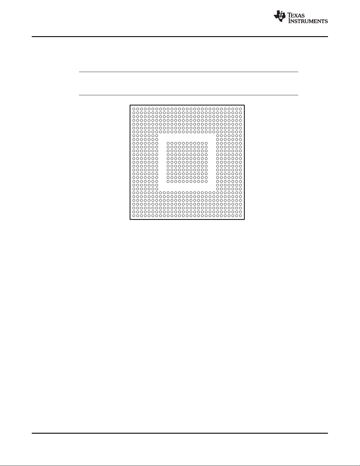
1.1 ZTZ BGA Package (Bottom View)
The TMS320C6472 devices are designed for a package temperature range of 0°C to 85°C (commercial
temperature range) or -40°C to 100°C (extended temperature range).
Extended temperature (A) range is available only on 500-MHz and 625-MHz devices.
www.ti.com
NOTE
Figure 1-1. ZTZ 737-Pin Ball Grid Array (BGA) Package (Bottom View)
2 Features Copyright © 2009–2010, Texas Instruments Incorporated
Submit Documentation Feedback
Product Folder Link(s) :TMS320C6472
Page 3

PRODUCTPREVIEW
www.ti.com
1.2 Description
The TMS320C6472 device is a Texas Instruments next-generation fixed-point digital signal processor
(DSP) targeting high-performance computing applications, including high-end industrial, mission-critical,
high-end image and video, communication, media gateways, and remote access servers. This device was
designed with these applications in mind. A common key requirement of these applications is the
availability of large on-chip memories to handle vast amounts of data during processing. With 768K-Byte
of shared RAM and 608K-Byte local L2 RAM per C64x+ Megamodule, the TMS320C6472 device can
eliminate the need for external memory, thereby reducing system power dissipation and system cost and
optimizing board density.
The TMS320C6472 device has six optimized TMS320C64x+™ megamodules, which combine high
performance with the lowest power dissipation per port. The TMS320C6472 device includes three different
speeds: 500 MHz, 625 MHz, and 700 MHz. The C64x+ megamodules are the highest-performance
fixed-point DSP generation in the TMS320C6000™ DSP platform. The C64x+ megamodule is based on
the third-generation high-performance, advanced VelociTI™ very-long-instruction-word (VLIW) architecture
developed by Texas Instruments (TI), making devices like TMS320C6472 an excellent choice for
applications including video and telecom infrastructure, imaging/medical, and wireless infrastructure (WI).
The C64x+™ devices are upward code-compatible from previous devices that are part of the C6000™
DSP platform.
The C64x+ megamodule core employs eight functional units, two register files, and two data paths. Like
the earlier C6000 devices, two of these eight functional units are multipliers or .M units. Each C64x+
megamodule core .M unit doubles the multiply throughput versus the C64x core by performing four
16-bit x 16-bit multiply-accumulates (MACs) every clock cycle. Thus, eight 16-bit x 16-bit MACs can be
executed every cycle on the C64x+ core. At a 500-MHz clock rate, this means 4000 16-bit MMACs can
occur every second. Moreover, each multiplier on the C64x+ megamodule core can compute one
32-bit x 32-bit MAC or four 8-bit x 8-bit MACs every clock cycle.
TMS320C6472
SPRS612E–JUNE 2009–REVISED OCTOBER 2010
The C64x+ megamodule integrates a large amount of on-chip memory organized as a two-level memory
system. The level-1 (L1) program and data memories on this C64x+ megamodule are 32KB each. This
memory can be configured as mapped RAM, cache, or some combination of the two. When configured as
cache, L1 program (L1P) is a direct mapped cache where as L1 data (L1D) is a two-way set associative
cache. The level 2 (L2) memory is shared between program and data space and is 608K-Byte in size. L2
memory can also be configured as mapped RAM, cache, or some combination of the two. The C64x+
megamodule also has a 32-bit peripheral configuration (CFG) port, an internal DMA (IDMA) controller, a
system component with reset/boot control, interrupt/exception control, a power-down control, and a
free-running 32-bit timer for time stamp.
The peripheral set includes: three Telecom Serial Interface Port (TSIPs); an 16/8 bit Universal Test and
Operations PHY Interface for Asynchronous Transfer Mode (ATM) Slave [UTOPIA Slave] port; two
10/100/1000 Ethernet media access controllers (EMACs), which provide an efficient interface between the
C6472 DSP core processor and the network; a management data input/output (MDIO) module (shared by
both EMACs) that continuously polls all 32 MDIO addresses in order to enumerate all PHY devices in the
system; a Serial RapidIO®with two 1x lanes and support for packet forwarding; a 32-bit DDR2 SDRAM
interface; 12 64-bit general-purpose timers; an inter-integrated circuit bus module (I2C); 16
general-purpose input/output ports (GPIO) with programmable interrupt/event generation modes; and a
16-bit multiplexed host-port interface (HPI16).
The C6472 device has a complete set of development tools which includes: a C compiler, an assembly
optimizer to simplify programming and scheduling, and a Windows®debugger interface for visibility into
source code execution.
Copyright © 2009–2010, Texas Instruments Incorporated Features 3
Submit Documentation Feedback
Product Folder Link(s) :TMS320C6472
Page 4
PRODUCTPREVIEW
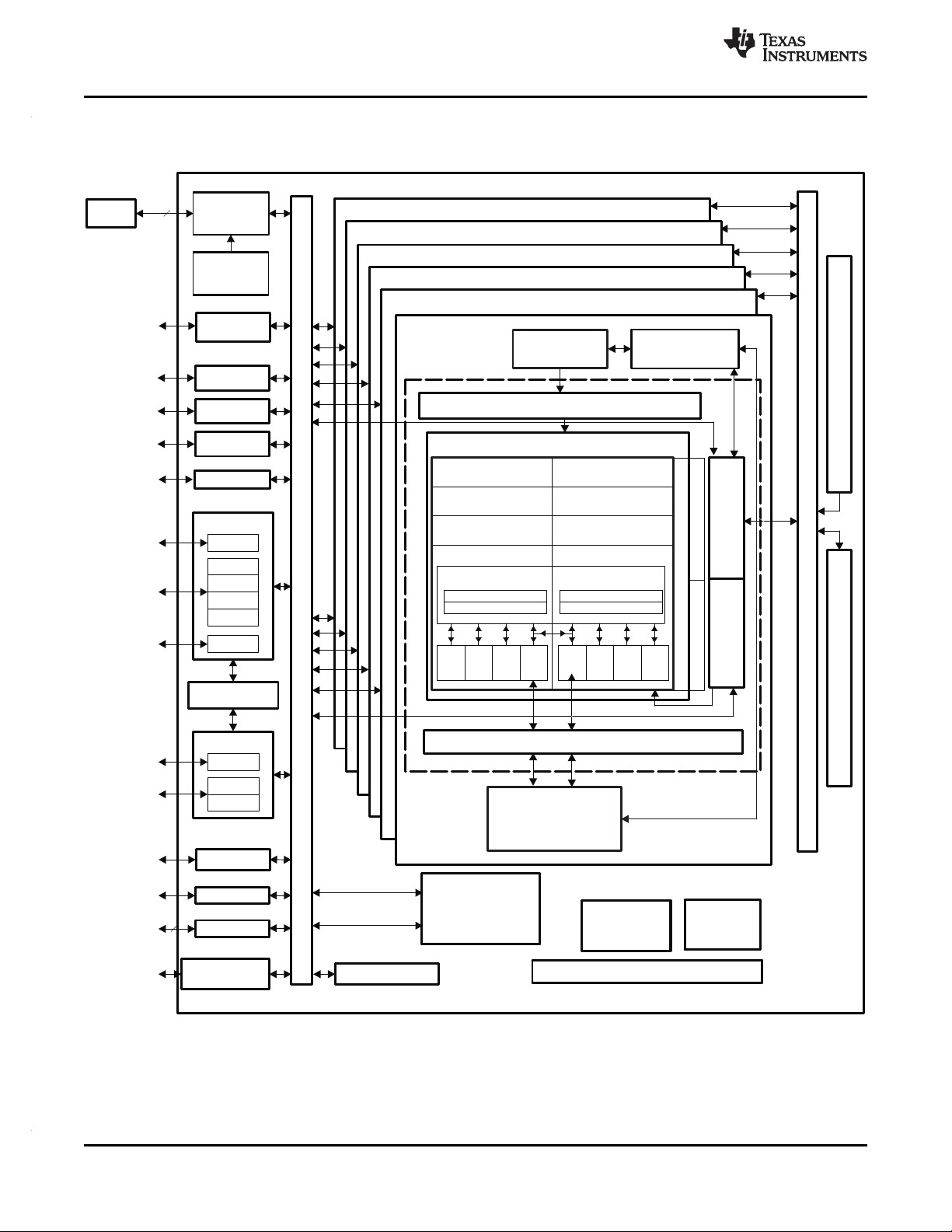
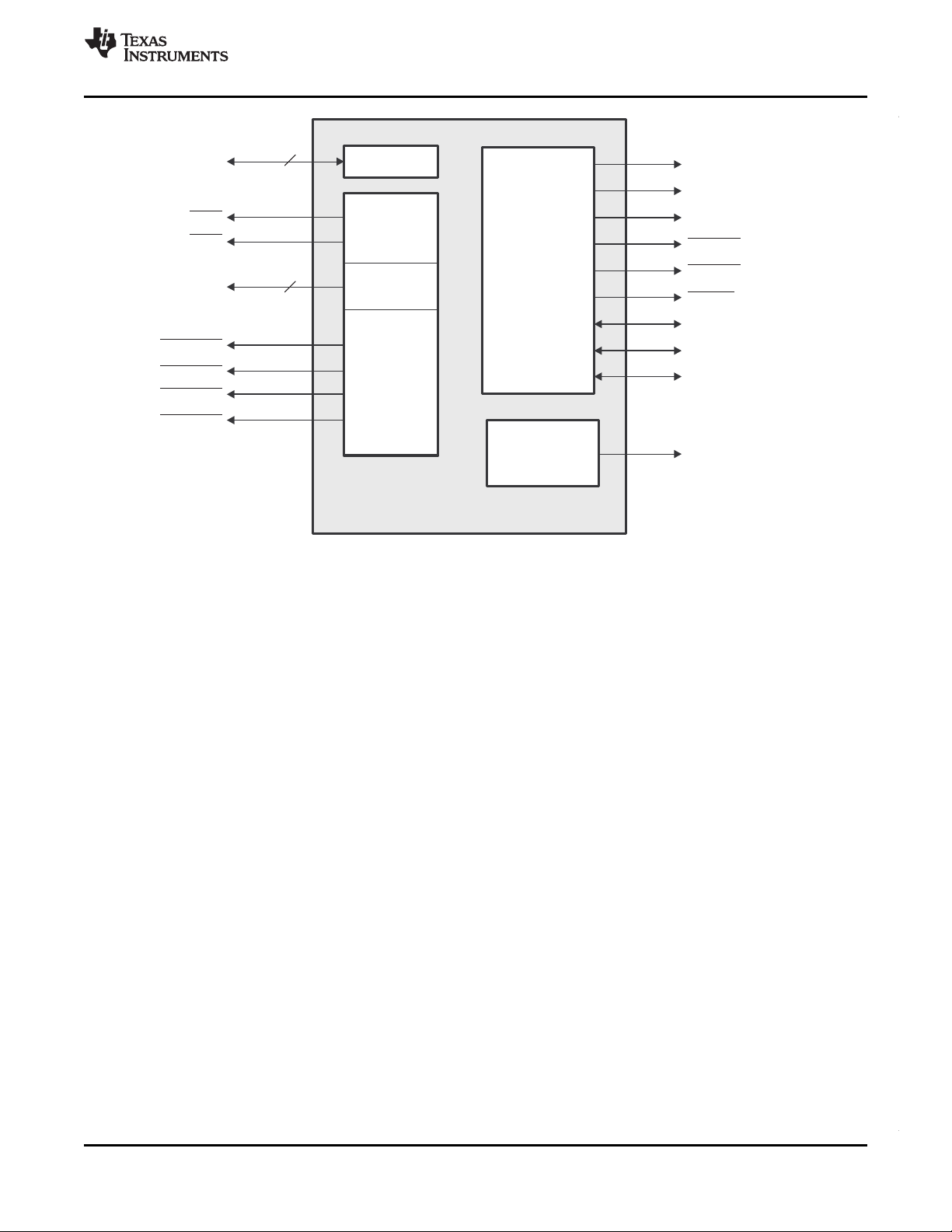
imerx[6thru11](A)
DSP Subsystem5
imerx[6thru11](A)
DSP Subsystem4
imerx[6thru11](A)
DSP Subsystem3
imerx[6thru11](A)
DSP Subsystem2
Timerx[6thru11](A)
DSP Subsystem1
Timerx[0-5]
(B)
EMAC1
SS-SMII
RGMII
Serial
RapidIO
DDR2
Memory
Controller
Power-Down
Logic
DSP Subsystem0
PLL1and
PLL1Controller
BootConfiguration
UTOPIA (16/8)
I2C
GPIO16
16
TSIP0
SharedL2Controller
TSIP1
HPI(16-bit)
DDR2
SDRAM
32
Timerx[6-11]
(Shared)
(A)(B)
PLL3and
PLL3
Controller
EDMA 3.0
System
©
)
PowerControl
C64x+DSP Core
DataPathB
BRegisterFile
InstructionFetch
DataPath A
A RegisterFile
.L1 .S1
.M1
xx
xx
.D1 .D2 .S2 .L2
InternalDMA
(IDMA)
L1P MemoryController (Memory Protect/BandwidthMgmt)
Instruction
Decode
16-/32-bit
InstructionDispatch
ControlRegisters
In-CircuitEmulation
SPLOOP Buffer
L1D MemoryController(MemoryProtect/BandwidthMgmt)
InterruptandExceptionController
EMAC0
32KBytes
L1P SRAM/Cache
Direct-Mapped
TSIP2
PLL2and
PLL2Controller
L2 SRAM/Cache
608KBytes
4-WaySet Assoc.
A31-A16
A15-A0
B31-B16
B15-B0
SS-SMII
GMII
MII
RGMII
RMII
32K-Bytes Total
L1DSRAM/Cache2-Way
Set-Associative
M
e
g
a
m
o
d
u
l
e
.M2
xx
xx
SL2RAM768K-Bytes
BootROM
L2MemoryController
(MemoryProtect/
BandwidthMgmt)
SwitchedCentralResource(SCR)
MDIO
RMII
TMS320C6472
SPRS612E–JUNE 2009–REVISED OCTOBER 2010
1.3 Functional Block Diagram
Figure 1-2 shows the functional block diagram of the C6472 device.
www.ti.com
A. Timers 6-11 are shared.
B. Each of the Timer peripherals are configurable as either one 64-bit general-purpose timer or two 32-bit
general-purpose timers or a watchdog timer.
C. System consists of Test, Emulation, Power Down, and Interrupt Controller.
4 Features Copyright © 2009–2010, Texas Instruments Incorporated
Figure 1-2. C6472 Functional Block Diagram
Submit Documentation Feedback
Product Folder Link(s) :TMS320C6472
Page 5

PRODUCTPREVIEW
www.ti.com
TMS320C6472
SPRS612E–JUNE 2009–REVISED OCTOBER 2010
1 Features ................................................... 1
1.1 ZTZ BGA Package (Bottom View) ................... 2
1.2 Description ........................................... 3
1.3 Functional Block Diagram ............................ 4
Revision History .............................................. 6
2 Device Overview ........................................ 7
2.1 Device Characteristics ............................... 7
2.2 CPU (DSP Core) Description ........................ 8
2.3 Memory Map Summary ............................. 11
2.4 Boot Mode Sequence .............................. 14
2.5 Pin Assignments .................................... 19
2.6 Signal Groups Description .......................... 23
2.7 Terminal Functions ................................. 29
2.8 Development ........................................ 53
3 Device Configuration ................................. 58
3.1 Device Configuration at Device Reset .............. 58
3.2 Device Configuration Register Descriptions ........ 59
3.3 Peripheral Selection After Device Reset ........... 62
3.4 Device Status Register (DEVSTAT) ................ 72
3.5 RMIIn Reset Registers (RMIIRESET0 and
RMIIRESET1) ...................................... 73
3.6 Memory Privilege Registers ........................ 74
3.7 Host and Inter-DSP Interrupt Registers ............ 77
3.8 Timer Event Manager Registers .................... 82
3.9 Reset and Boot Registers .......................... 84
3.10 JTAG ID Register Description ...................... 88
3.11 Silicon Revision ID Register Description ........... 88
4 System Interconnect .................................. 89
4.1 Internal Buses, Bridges, and Switch Fabrics ....... 89
4.2 Data Switch Fabric Connections ................... 90
4.3 Priority Allocation ................................... 93
4.4 Configuration Switch Fabric ........................ 93
5 C64x+ Megamodule ................................... 95
5.1 Memory Architecture ............................... 95
5.2 Memory Protection Support ........................ 99
5.3 Bandwidth Management .......................... 100
5.4 Power-Down Control .............................. 101
5.5 Megamodule Resets .............................. 101
5.6 Megamodule Revision ............................. 102
5.7 C64x+ Megamodule Register Descriptions ....... 103
5.8 CPU Revision ID .................................. 111
6 Device Operating Conditions ...................... 112
6.1 Absolute Maximum Ratings Over Operating Case
Temperature Range (Unless Otherwise Noted)
..................................................... 112
6.2 Recommended Operating Conditions ............. 113
6.3 Electrical Characteristics Over Recommended
Ranges of Supply Voltage and Operating Case
Temperature (Unless Otherwise Noted) .......... 115
7 C64x+ Peripheral Information and Electrical
Specifications ......................................... 117
7.1 Parameter Information ............................ 117
7.2 Recommended Clock and Control Signal Transition
Behavior ........................................... 118
7.3 Power Supplies .................................... 118
7.4 Power and Sleep Controller (PSC) ................ 120
7.5 Enhanced Direct Memory Access (EDMA3)
Controller .......................................... 123
7.6 Interrupts .......................................... 136
7.7 Reset Controller ................................... 140
7.8 PLL1 and PLL1 Controller ......................... 148
7.9 PLL2 and PLL2 Controller ......................... 160
7.10 PLL3 and PLL3 Controller ......................... 171
7.11 DDR2 Memory Controller ......................... 175
7.12 I2C Peripheral ..................................... 177
7.13 Host-Port Interface (HPI) Peripheral .............. 182
7.14 TSIP ............................................... 189
7.15 Ethernet MAC (EMAC) ............................ 215
7.16 Timers ............................................. 236
7.17 UTOPIA ........................................... 242
7.18 Serial RapidIO (SRIO) Port ....................... 247
7.19 General-Purpose Input/Output (GPIO) ............ 258
7.20 Emulation Features and Capability ............... 260
8 Mechanical Data ...................................... 263
8.1 Thermal Data ...................................... 263
8.2 Packaging Information ............................ 263
Copyright © 2009–2010, Texas Instruments Incorporated Contents 5
Submit Documentation Feedback
Product Folder Link(s) :TMS320C6472
Page 6

PRODUCTPREVIEW
TMS320C6472
SPRS612E–JUNE 2009–REVISED OCTOBER 2010
NOTE: Page numbers for previous revisions may differ from page numbers in the current version.
This revision history highlights the technical changes made to the document in this revision.
SEE ADDITIONS/MODIFICATIONS/DELETIONS
Section 5.1 Modified L2 memory Port 1 configuration
Added Table 5-1, SL2 Prefetch Enabled Memory Regions
Section 5.2 Modified fourth paragraph on privilege ID assignment
Modified Table 5-3, Available Memory Page Protection Scheme with Privilege ID
www.ti.com
Revision History
C6472 Revisions
6 Contents Copyright © 2009–2010, Texas Instruments Incorporated
Submit Documentation Feedback
Product Folder Link(s) :TMS320C6472
Page 7
PRODUCTPREVIEW
www.ti.com
2 Device Overview
Unless otherwise noted, all address locations in this document are stated in hexidecimal
numbers.
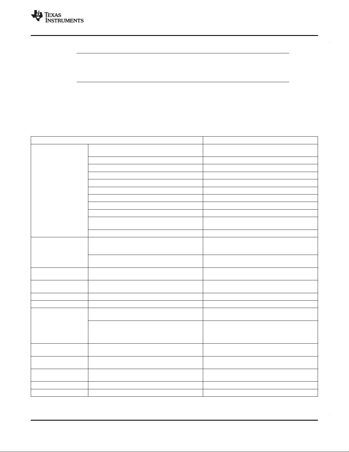
2.1 Device Characteristics
Table 2-1, provides an overview of the C6472 DSP. The table shows significant features of the C6472
device, including the capacity of on-chip RAM, the peripherals, the CPU frequency, and the package type
with pin count.
HARDWARE FEATURES C6472
DDR2 Memory Controller (32-bit bus width) [1.8 V I/O]
(clock source = CLKIN3)
EDMA (64 independent channels) 1
High-speed Serial RapidIO Port 2
Peripherals
Not all peripheral pins are
available at the same time
(for more detail, see
Section 3).
On-Chip Memory
CPU MegaModule Revision ID Register (MM_REVID.[15:0])
Revision ID Address 0181 2000
JTAG ID 0009 102Fh
Frequency MHz 500/625/700 MHz
Cycle Time ns 2 ns/1.6 ns
Voltage
PLL1 and
PLL1 Controller Options
PLL2 and CLKIN frequency multiplier
PLL2 Controller Options [EMAC support]
PLL3 and CLKIN frequency multiplier
PLL3 Controller Options [DDR2 Memory Controller support only]
BGA Package 24 x 24 mm 737-Pin Flip-Chip Plastic BGA (ZTZ)
Process Technology mm 0.09 mm
I2C 1
HPI (16 bit) 1
Telecom Serial Interface Port (TSIP) 3
UTOPIA (16/8-bit mode, 50-MHz, slave-only) 1
10/100/1000 Mb/s Ethernet MAC (EMAC) 2
Management Data Input/Output (MDIO) 1
64-bit Timers (Configurable)
General-Purpose Input/Output Port (GPIO) 16
Organization per C64x+ Megamodule 32K-Byte L1 Data Memory [SRAM/Cache]
Shared by all 6 C64x+ Megamodules
JTAG ID register
Address 02A8 0008
Core (V)
I/O (V)
CLKIN frequency multiplier Bypass (x1), x10-x32
TMS320C6472
SPRS612E–JUNE 2009–REVISED OCTOBER 2010
NOTE
Table 2-1. Characteristics of the C6472 Processor
1
12 (6 dedicated [0-5], 1 per core; 6 shared [6-11])
1 64-bit or 2 32-bit or WD each
32K-Byte L1 Program Memory [SRAM/Cache]
608K-Byte L2 Unified Memory [SRAM/Cache]
768K-byte SL2 Unified SRAM
768K-byte SL2 ROM
0003h
1.2 V (DDR2 EMIF)
1.0 V (500 MHz) / 1.1 V (625 MHz) / 1.2 V (700 MHz)
1.2 V [RapidIO],
1.5 V/1.8 V [EMAC RGMII],
1.8 V [DDR2 EMIF I/O], and
1.8 V and 3.3 V [I/O Supply Voltage]
x20
x20
Copyright © 2009–2010, Texas Instruments Incorporated Device Overview 7
Submit Documentation Feedback
Product Folder Link(s) :TMS320C6472
Page 8

PRODUCTPREVIEW
TMS320C6472
SPRS612E–JUNE 2009–REVISED OCTOBER 2010
Table 2-1. Characteristics of the C6472 Processor (continued)
HARDWARE FEATURES C6472
Product Status
Device Part Numbers TMX320C6472
(1) PRODUCT PREVIEW information concerns products in the formative or design phase of development. Characteristic data and other
specifications are design goals. Texas Instruments reserves the right to change or discontinue these products without notice.
(1)
Product Preview (PP), Advance Information (AI),
or Production Data (PD)
(For more details on the C64x+™ DSP part
numbering, see Figure 2-13)
PP
2.2 CPU (DSP Core) Description
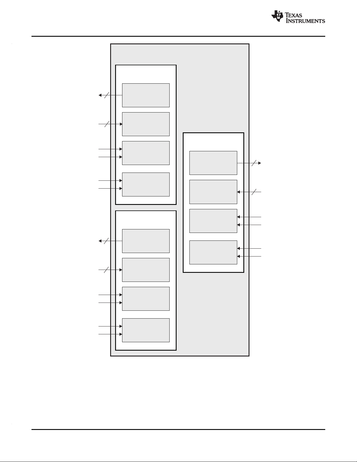
The C64x+ Central Processing Unit (CPU) consists of eight functional units, two register files, and two
data paths as shown in Figure 2-1. The two general-purpose register files (A and B) each contain
32 32-bit registers for a total of 64 registers. The general-purpose registers can be used for data or can be
data address pointers. The data types supported include packed 8-bit data, packed 16-bit data, 32-bit
data, 40-bit data, and 64-bit data. Values larger than 32 bits, such as 40-bit-long or 64-bit-long values are
stored in register pairs, with the 32 LSBs of data placed in an even register and the remaining 8 or
32 MSBs in the next upper register (which is always an odd-numbered register).
The eight functional units (.M1, .L1, .D1, .S1, .M2, .L2, .D2, and .S2) are each capable of executing one
instruction every clock cycle. The .M functional units perform all multiply operations. The .S and .L units
perform a general set of arithmetic, logical, and branch functions. The .D units primarily load data from
memory to the register file and store results from the register file into memory.
www.ti.com
The C64x+ CPU extends the performance of the C64x core through enhancements and new features.
Each C64x+ .M unit can perform one of the following each clock cycle: one 32 x 32 bit multiply, two
16 x 16 bit multiplies, two 16 x 32 bit multiplies, four 8 x 8 bit multiplies, four 8 x 8 bit multiplies with add
operations, and four 16 x 16 multiplies with add/subtract capabilities (including a complex multiply). There
is also support for Galois field multiplication for 8-bit and 32-bit data. Many communications algorithms
such as FFTs and modems require complex multiplication. The complex multiply (CMPY) instruction takes
four 16-bit inputs and produces a 32-bit real and a 32-bit imaginary output. There are also complex
multiplies with rounding capability that produce one 32-bit packed output that contains 16-bit real and
16-bit imaginary values. The 32 x 32 bit multiply instructions provide the extended precision necessary for
audio and other high-precision algorithms on a variety of signed and unsigned 32-bit data types.
The .L or Arithmetic Logic Unit now incorporates the ability to do parallel add/subtract operations on a pair
of common inputs. Versions of this instruction exist to work on 32-bit data or on pairs of 16-bit data
performing dual 16-bit add and subtracts in parallel. There are also saturated forms of these instructions.
The C64x+ core enhances the .S unit in several ways. In the C64x core, dual 16-bit MIN2 and MAX2
comparisons were only available on the .L units. On the C64x+ core they are also available on the .S unit
which increases the performance of algorithms that do searching and sorting. Finally, to increase data
packing and unpacking throughput, the .S unit allows sustained high performance for the quad 8-bit/16-bit
and dual 16-bit instructions. Unpack instructions prepare 8-bit data for parallel 16-bit operations. Pack
instructions return parallel results to output precision including saturation support.
Other new features include:
• SPLOOP - A small instruction buffer in the CPU that aids in creation of software pipelining loops where
multiple iterations of a loop are executed in parallel. The SPLOOP buffer reduces the code size
associated with software pipelining. Furthermore, loops in the SPLOOP buffer are fully interruptible.
• Compact Instructions - The native instruction size for the C6000 devices is 32 bits. Many common
instructions such as MPY, AND, OR, ADD, and SUB can be expressed as 16 bits if the C64x+
compiler can restrict the code to use certain registers in the register file. This compression is
performed by the code generation tools.
8 Device Overview Copyright © 2009–2010, Texas Instruments Incorporated
Submit Documentation Feedback
Product Folder Link(s) :TMS320C6472
Page 9

PRODUCTPREVIEW
www.ti.com
• Instruction Set Enhancements - As noted above, there are new instructions such as 32-bit
• Exception Handling - Intended to aid the programmer in isolating bugs. The C64x+ CPU is able to
• Privilege - Defines user and supervisor modes of operation, allowing the operating system to give a
• Time-Stamp Counter - Primarily targeted for Real-Time Operating System (RTOS) robustness, a
For more details on the C64x+ CPU and its enhancements over the C64x architecture, see the following
documents:
• TMS320C64x/C64x+ DSP CPU and Instruction Set Reference Guide (literature number SPRU732)
• TMS320C64x+ DSP Cache User's Guide (literature number SPRU862)
• TMS320C64x+ DSP Megamodule Reference Guide (literature number SPRU871)
• TMS320C64x Technical Overview (literature number SPRU395)
• TMS320C64x to TMS320C64x+ CPU Migration Guide (literature number SPRAA84)
TMS320C6472
SPRS612E–JUNE 2009–REVISED OCTOBER 2010
multiplications, complex multiplications, packing, sorting, bit manipulation, and 32-bit Galois field
multiplication.
detect and respond to exceptions, both from internally detected sources (such as illegal op-codes) and
from system events (such as a watchdog time expiration).
basic level of protection to sensitive resources. Local memory is divided into multiple pages, each with
read, write, and execute permissions.
free-running time-stamp counter is implemented in the CPU which is not sensitive to system stalls.
Copyright © 2009–2010, Texas Instruments Incorporated Device Overview 9
Submit Documentation Feedback
Product Folder Link(s) :TMS320C6472
Page 10

PRODUCTPREVIEW
src2
src2
.D1
.M1
.S1
.L1
longsrc
odddst
src2
src1
src1
src1
src1
evendst
evendst
odddst
dst1
dst
src2
src2
src2
longsrc
DA1
ST1b
LD1b
LD1a
ST1a
Data path A
Odd
register
file A
(A1, A3,
A5...A31)
Odd
register
fileB
(B1,B3,
B5...B31)
.D2
src1
dst
src2
DA2
LD2a
LD2b
src2
.M2
src1
dst1
.S2
src1
evendst
longsrc
odddst
ST2a
ST2b
longsrc
.L2
evendst
odddst
src1
Data pathB
Control Register
32MSB
32LSB
dst2
(A)
32MSB
32LSB
2x
1x
32LSB
32MSB
32LSB
32MSB
dst2
(B)
(B)
(A)
8
8
8
8
32
32
32
32
(C)
(C)
Even
register
file A
(A0, A2,
A4...A30)
Even
register
fileB
(B0,B2,
B4...B30)
(D)
(D)
(D)
(D)
TMS320C6472
SPRS612E–JUNE 2009–REVISED OCTOBER 2010
www.ti.com
A. On .M unit, dst2 is 32 MSB.
B. On .M unit, dst1 is 32 LSB.
C. On C64x CPU .M unit, src2 is 32 bits; on C64x+ CPU .M unit, src2 is 64 bits.
D. On .L and .S units, odd dst connects to odd register files and even dst connects to even register files.
10 Device Overview Copyright © 2009–2010, Texas Instruments Incorporated
Figure 2-1. TMS320C64x+™ CPU (DSP Core) Data Paths
Submit Documentation Feedback
Product Folder Link(s) :TMS320C6472
Page 11
PRODUCTPREVIEW
www.ti.com
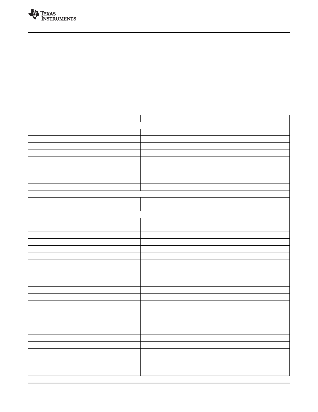
2.3 Memory Map Summary
Table 2-2 shows the memory map address ranges of the C6472 device. This table provides a combined
view of both local and global addresses. The C64x+ megamodule local memories have both local and
global addresses. The megamodule registers only have local addresses. Local addresses can only be
resolved within the megamodule. They cannot be accessed from outside the megamodule. All of the other
addresses listed in this table are global addresses. Global addresses can be accessed from any bus
master including all six C64x+ megamodules, the transfer controllers within the EDMA3 block, and any
peripheral that can master the bus.
Note: 1K = 1024, 1M = 1024K.
MEMORY BLOCK DESCRIPTION BLOCK SIZE (BYTES) HEX ADDRESS RANGE
Reserved 2M 00000000 - 001FFFFF
SL2 RAM (Local address map) 768K 00200000 - 002BFFFF
Reserved 5.25M 002C0000 - 007FFFFF
Local L2 SRAM 608K 00800000 - 00897FFF
Reserved 5M + 416K 00898000 - 00DFFFFF
Local L1P SRAM 32K 00E00000 - 00E07FFF
Reserved 992K 00E08000 - 00EFFFFF
Local L1D SRAM 32K 00F00000 - 00F07FFF
Reserved 992K 00F08000 - 00FFFFFF
Reserved 8M 01000000 - 017FFFFF
C64x+ Megamodule Registers 4M 01800000 - 01BFFFFF
Reserved 9M 01C00000 - 024FFFFF
TSIP0 256K 02500000 - 0253FFFF
TSIP1 256K 02540000 - 0257FFFF
TSIP2 256K 02580000 - 025BFFFF
Reserved 128K 025C0000 - 025DFFFF
Timer0 64K 025E0000 - 025EFFFF
Timer1 64K 025F0000 - 025FFFFF
Timer2 64K 02600000 - 0260FFFF
Timer3 64K 02610000 - 0261FFFF
Timer4 64K 02620000 - 0262FFFF
Timer5 64K 02630000 - 0263FFFF
Timer6 64K 02640000 - 0264FFFF
Timer7 64K 02650000 - 0265FFFF
Timer8 64K 02660000 - 0266FFFF
Timer9 64K 02670000 - 0267FFFF
Timer10 64K 02680000 - 0268FFFF
Timer11 64K 02690000 - 0269FFFF
Reserved 1.875M 026A0000 - 0287FFFF
HPI Control 128K 02880000 - 0289FFFF
Reserved 1M 028A0000 - 0299FFFF
PLL Controller 1 1K 029A0000 - 029A03FF
Reserved 127K 029A0400 - 029BFFFF
PLL Controller 2 1K 029C0000 - 029C03FF
TMS320C6472
SPRS612E–JUNE 2009–REVISED OCTOBER 2010
Table 2-2. C6472 Memory Map Summary
INTERNAL RAM AND ROM
C64x+ MEGAMODULE REGISTERS
CONTROL REGISTERS ON CONFIG SCR
Copyright © 2009–2010, Texas Instruments Incorporated Device Overview 11
Submit Documentation Feedback
Product Folder Link(s) :TMS320C6472
Page 12

PRODUCTPREVIEW
TMS320C6472
SPRS612E–JUNE 2009–REVISED OCTOBER 2010
MEMORY BLOCK DESCRIPTION BLOCK SIZE (BYTES) HEX ADDRESS RANGE
PLL Controller 3 1K 029C0400 - 029C07FF
Reserved 254K 029C0800 - 029FFFFF
EDMA3 - EDMA3CC 32K 02A00000 - 02A07FFF
Reserved 96K 02A08000 - 02A1FFFF
EDMA3 - EDMA3TC0 32K 02A20000 - 02A27FFF
EDMA3 - EDMA3TC1 32K 02A28000 - 02A2FFFF
EDMA3 - EDMA3TC2 32K 02A30000 - 02A37FFF
EDMA3 - EDMA3TC3 32K 02A38000 - 02A3FFFF
Reserved 256K 02A40000 - 02A7FFFF
Chip-Level Registers 128K 02A80000 - 02A9FFFF
Reserved 32K 02AA0000 - 02AA7FFF
Shared Memory Controller 32K 02AA8000 - 02AAFFFF
Boot Controller 32K 02AB0000 - 02AB7FFF
Reserved 160K 02AB8000 - 02ADFFFF
PSC 128K 02AE0000 - 02AFFFFF
GPIO 16K 02B00000 - 02B03FFF
I2C Data and Control 16K 02B04000 - 02B07FFF
Reserved 224K 02B08000 - 02B3FFFF
UTOPIA 256K 02B40000 - 02B7FFFF
Reserved 256K 02B80000 - 02BBFFFF
UTOPIA-PDMA (PIM) Configuration 256K 02BC0000 - 02BFFFFF
Reserved 128K 02C00000 - 02C1FFFF
SMCP0 16K 02C20000 - 02C23FFF
SMCP1 16K 02C24000 - 02C27FFF
SMCP2 16K 02C28000 - 02C2BFFF
SMCP3 16K 02C2C000 - 02C2FFFF
SMCP4 16K 02C30000 - 02C33FFF
SMCP5 16K 02C34000 - 02C37FFF
Reserved 32K 02C38000 - 02C3FFFF
ETB0 4K 02C40000 - 02C40FFF
ETB1 4K 02C41000 - 02C41FFF
ETB2 4K 02C42000 - 02C42FFF
ETB3 4K 02C43000 - 02C43FFF
ETB4 4K 02C44000 - 02C44FFF
ETB5 4K 02C45000 - 02C45FFF
Reserved 232K 02C46000 - 02C7FFFF
EMAC0 Control 4K 02C80000 - 02C80FFF
EMAC0 Control Module Registers 2K 02C81000 - 02C817FF
MDIO Control Registers 2K 02C81800 - 02C81FFF
EMAC0 Descriptor Memory 8K 02C82000 - 02C83FFF
Reserved 240K 02C84000 - 02CBFFFF
EMAC1 Control 4K 02CC0000 - 02CC0FFF
EMAC1 Control Module Registers 2K 02CC1000 - 02CC17FF
EMIC0 1K 02CC1800 - 02CC1BFF
EMIC1 1K 02CC1C00 - 02CC1FFF
EMAC1 Descriptor Memory 8K 02CC2000 - 02CC3FFF
Reserved 240K 02CC4000 - 02CFFFFF
www.ti.com
Table 2-2. C6472 Memory Map Summary (continued)
12 Device Overview Copyright © 2009–2010, Texas Instruments Incorporated
Submit Documentation Feedback
Product Folder Link(s) :TMS320C6472
Page 13
PRODUCTPREVIEW
www.ti.com
Table 2-2. C6472 Memory Map Summary (continued)
MEMORY BLOCK DESCRIPTION BLOCK SIZE (BYTES) HEX ADDRESS RANGE
RapidIO Control Registers 256K 02D00000 - 02D3FFFF
Reserved 768K 02D40000 - 02DFFFFF
RapidIO Descriptor Memory 16K 02E00000 - 02E03FFF
Reserved 209M + 1008K 02E04000 - 0FFFFFFF
Reserved 2M 10000000 - 101FFFFF
SL2 RAM (through DSP0) 768K 10200000 - 102BFFFF
Reserved 5.25M 102C0000 - 107FFFFF
DSP0 L2 SRAM 608K 10800000 - 10897FFF
Reserved 5M + 416K 10898000 - 10DFFFFF
DSP0 L1P SRAM 32K 10E00000 - 10E07FFF
Reserved 992K 10E08000 - 10EFFFFF
DSP0 L1D SRAM 32K 10F00000 - 10F07FFF
Reserved 2M + 992K 10F08000 - 111FFFFF
SL2 RAM (through DSP1) 768K 11200000 - 112BFFFF
Reserved 5.25M 112C0000 - 117FFFFF
DSP1 L2 SRAM 608K 11800000 - 11897FFF
Reserved 5M + 416K 11898000 - 11DFFFFF
DSP1 L1P SRAM 32K 11E00000 - 11E07FFF
Reserved 992K 11E08000 - 11EFFFFF
DSP1 L1D SRAM 32K 11F00000 - 11F07FFF
Reserved 2M + 992K 11F08000 - 121FFFFF
SL2 RAM (through DSP2) 768K 12200000 - 122BFFFF
Reserved 5.25M 122C0000 - 127FFFFF
DSP2 L2 SRAM 608K 12800000 - 12897FFF
Reserved 5M + 416K 12898000 - 12DFFFFF
DSP2 L1P SRAM 32K 12E00000 - 12E07FFF
Reserved 992K 12E08000 - 12EFFFFF
DSP2 L1D SRAM 32K 12F00000 - 12F07FFF
Reserved 2M + 992K 12F08000 - 131FFFFF
SL2 RAM (through DSP3) 768K 13200000 - 132BFFFF
Reserved 5.25M 132C0000 - 137FFFFF
DSP3 L2 SRAM 608K 13800000 - 13897FFF
Reserved 5M + 416K 13898000 - 13DFFFFF
DSP3 L1P SRAM 32K 13E00000 - 13E07FFF
Reserved 992K 13E08000 - 13EFFFFF
DSP3 L1D SRAM 32K 13F00000 - 13F07FFF
Reserved 2M + 992K 13F08000 - 141FFFFF
SL2 RAM (through DSP4) 768K 14200000 - 142BFFFF
Reserved 5.25M 142C0000 - 147FFFFF
DSP4 L2 SRAM 608K 14800000 - 14897FFF
Reserved 5M + 416K 14898000 - 14DFFFFF
DSP4 L1P SRAM 32K 14E00000 - 14E07FFF
Reserved 992K 14E08000 - 14EFFFFF
DSP4 L1D SRAM 32K 14F00000 - 14F07FFF
Reserved 2M + 992K 14F08000 - 151FFFFF
SL2 RAM (through DSP5) 768K 15200000 - 152BFFFF
TMS320C6472
SPRS612E–JUNE 2009–REVISED OCTOBER 2010
INTERNAL RAM (GLOBAL MEMORY MAP)
Copyright © 2009–2010, Texas Instruments Incorporated Device Overview 13
Submit Documentation Feedback
Product Folder Link(s) :TMS320C6472
Page 14
PRODUCTPREVIEW
TMS320C6472
SPRS612E–JUNE 2009–REVISED OCTOBER 2010
Table 2-2. C6472 Memory Map Summary (continued)
MEMORY BLOCK DESCRIPTION BLOCK SIZE (BYTES) HEX ADDRESS RANGE
Reserved 5.25M 152C0000 - 157FFFFF
DSP5 L2 SRAM 608K 15800000 - 15897FFF
Reserved 5M + 416K 15898000 - 15DFFFF
DSP5 L1P SRAM 32K 15E00000 - 15E07FFF
Reserved 992K 15E08000 - 15EFFFFF
DSP5 L1D SRAM 32K 15F00000 - 15F07FFF
Reserved 161M + 992K 15F08000 - 1FFFFFFF
DATA SPACE ON DMA
Reserved 1408M 20000000 - 77FFFFFF
DDR2 EMIF Config 128M 78000000 - 7FFFFFFF
Reserved 1536M 80000000 - DFFFFFFF
CE0-CE1 DDR2 SDRAM 512M E0000000 - FFFFFFFF
2.4 Boot Mode Sequence
The boot sequence is a process by which the DSP's internal memory is loaded with program and data
sections and the DSP's internal registers are programmed with predetermined values. The boot sequence
is started automatically after each power-on, warm, and system reset. For more details on the initiators of
these resets, see Section 7.7, Reset Controller.
www.ti.com
There are several methods by which the memory and register initialization can take place. Each of these
methods is referred to as a boot mode. The boot mode to be used is selected at reset through the
BOOTMODE[3:0] pins.
2.4.1 Boot Modes Supported
The TMS320C6472 has a dedicated Boot Controller, which is responsible for managing the boot process
for single and multiple C64x+ megamodule core boots. There are two types of resets on the C6472
device:
1. Device-level Resets (Global Resets)
– Power-on Reset; initiated by POR
– Chip-level Warm Reset (or Device Reset); initiated by RESET
– System Reset; initiated by a watchdog timeout or emulation
2. C64x+ megamodule-level Resets (Local Resets)
– External C64x+ megamodule selectable LRESET
– Local reset of the C64x+ megamodule initiated by on-chip Reset Controller
– Power Sleep Controller initiated by local C64x+ megamodule reset
After POR and RESET asserted resets, the boot controller selects the boot mode based on the status of
BOOTMODE[3:0] pins. When a system reset occurs, the boot mode used is determined by the
BOOTMODE field in the DEVSTAT register. All possible bootmodes are listed in Table 2-3. For a detailed
explanation of this operation, see the TMS320C645x/C647x Bootloader User's Guide (literature number
SPRUEC6).
Following a device-level reset, each C64x+ megamodule core can set its boot mode choice for
subsequent local resets using the registers BOOTMODE0 through BOOTMODE5 to either immediate boot
mode or host boot mode. The default values of these registers are set to immediate boot mode.
14 Device Overview Copyright © 2009–2010, Texas Instruments Incorporated
Submit Documentation Feedback
Product Folder Link(s) :TMS320C6472
Page 15

PRODUCTPREVIEW
www.ti.com
BOOTMODE[3:0] DESCRIPTION TYPE CFGGP[4:0]
0 (0000) Immediate boot Immediate Boot Don’t Care
1 (0001) Host boot (HPI) Host Don’t Care
2 (0010) Master I2C boot for I2C address 50h ROM
3 (0011) Master I2C boot for I2C address 51h ROM
4 (0100) Slave I2C boot ROM
5 (0101) ROM
6 (0110) ROM
7 (0111) ROM
8 (1000) ROM
9 (1001) (mode and speed determined by ROM
10 (1010) (mode and speed determined by ROM
11 (1011) RIO1 ROM
12 (1100) RIO2 ROM
UTOPIA boot 8-bit PLLx10 of main PHY ID
PLLCTL
UTOPIA boot 8-bit PLLx20 of main PHY ID
PLLCTL
UTOPIA boot 16-bit PLLx10 of main PHY ID
PLLCTL
UTOPIA boot 16-bit PLLx20 of main PHY ID
PLLCTL
Ethernet MAC Port 0 boot
MACSEL0 pins)
Ethernet MAC Port 1 boot
MACSEL1 pins)
TMS320C6472
SPRS612E–JUNE 2009–REVISED OCTOBER 2010
Table 2-3. Boot Mode Operation
CFGGP[4] =
0 PLLx9 mode of main PLLCTL is selected
1 PLLx19 mode of main PLLCTL is
selected
CFGGP[3:0] = Boot PARAM index
CFGGP[4] =
0 PLLx9 mode of main PLLCTL is selected
1 PLLx19 mode of main PLLCTL is
selected
CFGGP[3:0] = Boot PARAM index
CFGGP[4] =
0 PLLx9 mode of main PLLCTL is selected
1 PLLx19 mode of main PLLCTL is
selected
CFGGP[3:0] = Don’t Care
CFGGP[4] =
0 PLLx10 mode of main PLLCTL is
selected
1 PLLx20 mode of main PLLCTL is
selected
CFGGP[3:0]: Device ID (when RMII is selected,
CFGGP[3] controls speed - 1 for 100 Mbs, 0 for 10
Mbps - and Device ID[3] is 0)
CFGGP[4] =
0 PLLx10 mode of main PLLCTL is
selected
1 PLLx20 mode of main PLLCTL is
selected
CFGGP[3:0]: Device ID (when RMII is selected,
CFGGP[3] controls speed - 1 for 100 Mbs, 0 for 10
Mbps - and Device ID[3] is 0)
CFGGP[4] =
0 PLLx10 mode of main PLLCTL is
selected
1 PLLx20 mode of main PLLCTL is
selected
CFGGP [3:0]: Node (1111b for default)
CFGGP[4] =
0 PLLx10 mode of main PLLCTL is
selected
1 PLLx20 mode of main PLLCTL is
selected
CFGGP [3:0]: Node (1111b for default)
Copyright © 2009–2010, Texas Instruments Incorporated Device Overview 15
Submit Documentation Feedback
Product Folder Link(s) :TMS320C6472
Page 16
PRODUCTPREVIEW
TMS320C6472
SPRS612E–JUNE 2009–REVISED OCTOBER 2010
Table 2-3. Boot Mode Operation (continued)
BOOTMODE[3:0] DESCRIPTION TYPE CFGGP[4:0]
CFGGP[4] =
0 PLLx10 mode of main PLLCTL is
13 (1101) RIO3 ROM
CFGGP [3:0]: Node (1111b for default)
CFGGP[4] =
14 (1110) RIO4 ROM
CFGGP [3:0]: Node (1111b for default)
15 (1111) Reserved ROM Reserved
• Immediate boot
When immediate boot is selected after global reset, the C64x+ megamodule core executes directly
from the internal L2 SRAM address programmed in the DSP_BOOT_ADDRx register. Note: device
operation is undefined if invalid code is address programmed in the DSP_BOOT_ADDRx register.
Executing invalid code may prevent connection by an emulator.
The default start addresses for megamodule core 0-5 boot are listed in Table 2-4.
selected
1 PLLx20 mode of main PLLCTL is
selected
0 PLLx10 mode of main PLLCTL is
selected
1 PLLx20 mode of main PLLCTL is
selected
www.ti.com
MEGAMODULE ADDRESSES FOR ADDRESSES FOR
CORE NAME DEVICE RESET/ DEVICE RESET/
Megamodule 0x0080_0000 0x0010_0000 0x0010_0000, if the device
Core 0 reset was boot mode 2-15;
Megamodule 0x0080_0000 0x0080_0000 0x0080_0000
Core 1
Megamodule 0x0080_0000 0x0080_0000 0x0080_0000
Core 2
Megamodule 0x0080_0000 0x0080_0000 0x0080_0000
Core 3
Megamodule 0x0080_0000 0x0080_0000 0x0080_0000
Core 4
Megamodule 0x0080_0000 0x0080_0000 0x0080_0000
Core 5
For boot mode 1, these addresses can be modifed by the host before it releases each megamodule
core from reset; for details, see Section 3.9.5. For boot mode 2-15, it is possible to have megamodule
core 0 modify the default address of megamodule core 1-5 before it releases each megamodule core
from reset; for details, see Section 2.4.1. For local reset, if all cores are required to begin from a
particular address, the default addresses have to be modified. One example is that only the
megamodule core 0's default address is modified to match megamodule core 1-5.
• Host boot
If host boot is selected after global reset, all C64x+ megamodule cores are internally "held in reset"
while the remainder of the device (including all memory subsystems of the C64x+ megamodule) is
released from reset. During this period, an external host can initialize the C6472 device memory space
(shared memory as well as the C64x+ megamodule memory), as necessary through an HPI interface,
including internal configuration registers such as those that control the DDR2 or other peripherals.
Once the host is finished with all necessary initialization, it must write a 1 to bit fields BC0 through BC5
of the BOOT_COMPLETE_STAT register (inside the Boot Controller) indicating boot complete of the
16 Device Overview Copyright © 2009–2010, Texas Instruments Incorporated
Table 2-4. Megamodule Core 0-5 Boot Start Addresses
DEFAULT START DEFAULT START
BOOT MODE 0-1 BOOT MODE 2-15
Submit Documentation Feedback
Product Folder Link(s) :TMS320C6472
DEFAULT START
ADDRESSES FOR
LOCAL RESET
otherwise 0x0080_0000
Page 17

PRODUCTPREVIEW
www.ti.com
corresponding C64x+ megamodule. This transition causes the Boot Controller to bring the C64x+
megamodule core out of the "held-in-reset" state. The CPU then begins execution from the internal L2
SRAM address programmed in the DSP_BOOT_ADDRx register. All memory may be written to and
read by the host. This allows for the host to verify what it sends to the DSP, if required.
For the C6472 device, only the Host Port Interface (HPI) peripheral can be used for host boot. PLL1,
which provides CPU/6 clock to the HPI module, will initially be running in bypass mode. Therefore, the
HPI interface will be very slow and HRDY must be observed. Initial HPI accesses can configure PLL1
for full-speed operation to make HPI accesses shorter.
• Master I2C boot
After global reset, the C64x+ megamodule core 0 comes out of RESET and starts executing the
shared ROM code from the address provided by the Boot Controller based on the I2C boot mode
selection. Then C64x+ megamodule core 0 configures I2C and acts as a master to the I2C bus and
copies data from an I2C EPROM or a device acting as an I2C slave to the DSP using a predefined
boot table format. The destination address and length are contained within the boot table. After
initializing the on-chip memory to the known state and initializing the start address of the other C64x+
megamodule cores, C64x+ megamodule core 0 brings the other cores out of reset by writing a 1 to bit
fields BC1 through BC5 of the BOOT_COMPLETE_STAT register. After this, C64x+ megamodule
cores 1 through 5 start executing from the start address provided by C64x+ megamodule core 0.
• Slave I2C boot
A Slave I2C boot is also implemented, which programs the DSP as an I2C slave. A DSP in I2C slave
mode will never transmit on the I2C bus. The slave DSP must first receive a three-word transmission
from the master. This transmission includes a 16-bit length field (length is in bytes, should be 6 for this
block), a 16-bit checksum field for which a value of zero means ignore the checksum, and the 16-bit
options field described in the boot parameter table for standard I2C boot. This option field informs the
slave what information is contained in the next data blocks. Typically, the option field is set to 1 to
indicate boot tables will be received next. Only core 0 is active during the boot process. Using the
slave I2C boot, a single DSP or device acting as an I2C master can simultaneously boot multiple slave
DSPs connected to the same I2C bus. Note that the master DSP may require booting via an I2C
EEPROM before acting as a master and booting other DSPs.
• Ethernet MAC boot
When BOOTMODE [3:0] = 1001 is selected, Ethernet MAC boot is initiated on EMAC0 with the mode
specified by the MACSEL0[2:0] pins. Alternately, when BOOTMODE [3:0] = 1010 is selected, Ethernet
MAC boot is initiated on EMAC1 with the mode specified by the MACSEL1[1:0] pins.
After reset, the C64x+ megamodule core 0 comes out of RESET and starts executing the shared ROM
code from the address provided by the Boot Controller based on the Ethernet boot mode selection
(1001b or 1010b). The C64x+ megamodule core 0 configures the appropriate Ethernet MAC and
brings the code image into the on-chip memory via the protocol defined. After initializing the on-chip
memory to the known state and initializing the start address of the other C64x+ megamodule cores (1
through 5), C64x+ megamodule core 0 brings the other cores out of reset by writing a 1 to bit fields
BC1 through BC5 of the BOOT_COMPLETE_STAT register. After this, C64x+ megamodule cores 1
through 5 start executing from the start address provided by C64x+ megamodule core 0.
• Serial RapidIO boot
After reset, the C64x+ megamodule core 0 comes out of RESET and starts executing the shared ROM
code from the address provided by the Boot Controller based on the Serial RapidIO boot mode
selection (1011b, 1100b, 1101b, or 1110b). The C64x+ megamodule core 0 configures Serial RapidIO
and EDMA, if required, and brings the code image into the on-chip memory via the protocol defined by
the boot method (SRIO bootloader). After initializing the on-chip memory to the known state and
initializing the start address of the other C64x+ megamodule cores (1 through 5), C64x+ megamodule
core 0 brings the other cores out of reset by writing a 1 to bit fields BC1 through BC5 of the
BOOT_COMPLETE_STAT register. After this, the C64x+ megamodule cores 1 through 5 start
executing from the start address provided by C64x+ megamodule core 0.
• UTOPIA boot
TMS320C6472
SPRS612E–JUNE 2009–REVISED OCTOBER 2010
Copyright © 2009–2010, Texas Instruments Incorporated Device Overview 17
Submit Documentation Feedback
Product Folder Link(s) :TMS320C6472
Page 18

PRODUCTPREVIEW
TMS320C6472
SPRS612E–JUNE 2009–REVISED OCTOBER 2010
After reset, the C64x+ megamodule core 0 comes out of RESET and starts executing the shared ROM
code from the address provided by the Boot Controller based on the UTOPIA boot mode selection
(0101b, 0110b, 0111b, 1000b). The C64x+ megamodule core 0 configures the UTOPIA and brings the
code image into the on-chip memory via the protocol defined. After initializing the on-chip memory to
the known state and initializing the start address of the other C64x+ megamodule cores (1 through 5),
C64x+ megamodule core 0 brings the other cores out of reset by writing a 1 to bit fields ofBC1 through
BC5 the BOOT_COMPLETE_STAT register. After this, C64x+ megamodule cores 1 through 5 start
executing from the start address provided by C64x+ megamodule core 0.
After local resets, the C6472 device supports two boot modes via BOOTMODE0-BOOTMODE5
device-level registers:
• Immediate boot
When immediate boot is selected after global reset, the C64x+ megamodule core (x) executes directly
from the internal L2 SRAM address programmed in the DSP_BOOT_ADDRx register upon being given
a local reset. Note: device operation is undefined if invalid code is address programmed in the
DSP_BOOT_ADDRx register. Executing invalid code may prevent connection by an emulator.
• Host boot
If host boot is selected after global reset, the C64x+ megamodule core (x) is internally "held in reset"
while the remainder of the C64x+ megamodule is released from reset upon being given a local reset.
During this period, an external host can initialize the C64x+ megamodule (x) memory space, as
necessary, through an HPI interface. Once the host is finished with all necessary initialization, it must
write a 1 to the corresponding bit field BCx of the BOOT_COMPLETE_STAT register (inside the Boot
Controller) indicating boot complete of the corresponding C64x+ megamodule. This transition causes
the Boot Controller to bring the C64x+ megamodule core out of the "held-in-reset" state. The core (x)
then begins execution from the internal L2 SRAM programmed in the DSP_BOOT_ADDRx register. All
memory may be written to and read by the host. This allows for the host to verify what it sends to the
DSP, if required.
www.ti.com
2.4.2 BOOTACTIVE
The output pin, BOOTACTIVE, is asserted upon reset and de-asserted on boot complete. In the case of
BOOTMODE 0, all cores are released from reset immediately. BOOTACTIVE also goes low within a small
number of cycles, as all cores are out of reset and running. In the case of BOOTMODE 1, the host needs
to write to the boot complete bit in the BOOT_COMPLETE_STAT register corresponding to each C64x+
megamodule that is to be taken out of reset. BOOTACTIVE will be high if any cores are held in reset. In
the case of any other boot, core 0 comes out of RESET immediately, but all other cores are still in
RESET, so BOOTACTIVE will be high. The ROM code will not write to either the
BOOT_COMPLETE_STAT or the BOOT_ADDRESS register unless explicitly directed to do so by the data
provided in the boot process. Any active core can set bits in BOOT_COMPLETE_STAT at any time to
begin code execution on inactive cores. BOOTACTIVE will go low after the boot complete bit (BCx) in the
BOOT_COMPLETE_STAT register is set for all six cores. For a detailed explanation of this operation, see
the TMS320C645x/C647x Bootloader User's Guide (literature number SPRUEC6).
18 Device Overview Copyright © 2009–2010, Texas Instruments Incorporated
Submit Documentation Feedback
Product Folder Link(s) :TMS320C6472
Page 19
PRODUCTPREVIEW
AG
AF
AE
AD
AC
AB
AA
Y
W
V
U
T
R
13121110987654321
13121110987654321
AH
RSV11
14 15
14 15
AG
AF
AE
AD
AC
AB
AA
Y
W
V
U
T
R
AH
AJ
DV
DD33
V
SS
AJ
MRXD07
DV
DD33
V
SS
MTXD05/
RMTXD11
V
SS
MTCLK0/
REFCLK0/
SREFCLK0
MRXD03/
SRXSYNC1
MRXD02/
SRXD1
DV
DD33
MRXD06/
RMRXER1
V
SS
RGRD13
DV
DD15
RGRD12
V
SS
CLKIN2
MTXD01/
RMTXD01/
STXSYNC0
GMDIO
MRXD04/
RMRXD10
DV
DD33
MRXD00/
RMRXD00/
SRXD0
RSV10
MACSEL11
LENDIANTR21
TX14
V
SS
TR17 TR16 TX27 RSV12
MACSEL01
GMTCLK0/
REFCLK1/
SREFCLK1
MRXD05/
RMRXD11
MTXD02/
STXD1
GMDCLK
MRCLK0/
SRXCLK1
MRXD01/
RMRXD01/
SRXSYNC0
MTXD07/
STXCLK0
DV
DD15MON
AV
DDA2
RGRXC1
FSA1
TX11 TR22
TX20
MACSEL10
MACSEL02
RSV09
MTXD00/
RMTXD00/
STXD0
MTXD03/
STXSYNC1
MCRS0/
RMCRSDV0
MTXEN0/
RMRTXEN0
MRXER0/
RMRXER0/
SRXCLK0
HHV15EN
PTV15P RGRD11
RGRD10
PTV15NRSV14
MTDX06/
RMTXEN1
MRXDV0/
RMCRSDV1
CV
DD
CV
DDMON
MCOL0
MTDX04/
RMTXD10/
STXCLK1
MACSEL00
TX26
TR24
TR23
DV
DD33
V
SS
TX16
TX15 TX13
TR26
TX22
V
SS
DV
DD33
V
SS
DV
DD33
V
SS
DV
DD33
V
SS
DV
DD33
V
SS
DV
DD15
V
SS
DV
DD15
DV
DD33
V
SS
DV
DD33
V
SS
DV
DD33
V
SS
DV
DD33
V
SS
CLKB1 TR15
TR10
TX24
TX23
V
SS
DV
DD33
TR11
TR27
TR20
V
SS
DV
DD33
DV
DD33
V
SS
TR02 CLKB2
TX10
TR25
TX21
FSB0
TX17
TR12 TX12
TX25
V
SS
DV
DD33
FSA2
TR14
TR13
DV
DD33
V
SS
V
SS
DV
DD33
V
SS
CV
DD
V
SS
CV
DD
V
SS
CV
DD
V
SS
CV
DD
V
SS
CV
DD
V
SS
CV
DD
V
SS
CV
DD
V
SS
CV
DD
V
SS
CV
DD
V
SS
CV
DD
V
SS
CV
DD
V
SS
CV
DD
V
SS
CV
DD
V
SS
CV
DD
V
SS
CV
DD
V
SS
CV
DD
V
SS
CV
DD
V
SS
CV
DD
TR03
FSA0 CLKA1
CLKA2
DV
DD33MON
V
SS
DV
DD33
TR07
TX00 CLKA0 TR01 FSB2
DV
DD33
V
SS
V
SS
DV
DD33
DV
DD33
V
SS
V
SS
DV
DD33
TR00
TX02
FSB1
TX05 TR05
TR06
CLKB0
TX01
www.ti.com
2.5 Pin Assignments
2.5.1 Pin Map
Figure 2-2 through Figure 2-5 show the C6472 pin assigments in four quadrants (A, B, C, and D).
TMS320C6472
SPRS612E–JUNE 2009–REVISED OCTOBER 2010
Copyright © 2009–2010, Texas Instruments Incorporated Device Overview 19
Figure 2-2. C6472 Pin Map (Bottom View) [Quadrant A]
Submit Documentation Feedback
Product Folder Link(s) :TMS320C6472
Page 20
PRODUCTPREVIEW
AG
AF
AE
AD
AC
AB
AA
Y
W
V
U
T
R
28272625242322212019181716
28272625242322212019181716
AH
AJ
29
29
AG
AF
AE
AD
AC
AB
AA
Y
W
V
U
T
R
AH
AJ
V
SS
CV
DD
V
SS
CV
DD
V
SS
DV
DD33
V
SS
CV
DD
V
SS
CV
DD
V
SS
CV
DD
V
SS
CV
DD
V
SS
CV
DD2
V
SS
DV
DDD
V
SS
CV
DD
V
SS
CV
DD
V
SS
CV
DD2
V
SS
CV
DD
V
SS
CV
DD
V
SS
DV
DDD
V
SS
CV
DD
V
SS
CV
DD
V
SS
CV
DD2
DV
DD33
V
SS
V
SS
DV
DD33
V
SS
DV
DD15
V
SS
DV
DD15
V
SS
DV
DD15
V
SS
DV
DD15
V
SS
DV
DD15
V
SS
DV
DD15
V
SS
DV
DD33
DV
DD33
V
SS
AV
DDA
AV
DDA
V
SS
DV
DD33
V
SS
V
SS
DV
DD33
V
SS
AV
DDT
V
SS
V
SS
V
SS
DV
DDR
RSV20
V
SS
RIOCLKN RIOTXN1 RIORXP1
V
SS
RIOCLKP RIOTXP1 RIORXN1RIOEN
CV
DD
V
SS
TIM02 TIMI1TIMIO
UXADDR4
UXADDR2 UXADDR0UXADDR1
UXADDR3
URADDR4
URADDR2 URADDR0URADDR1URADDR3
URSOC
URDATA2 URDATA0URDATA1UXENB
URDATA5
URDATA3URDATA4
DV
DD33
V
SS
URDATA10
URDATA8URDATA9
URDATA6URDATA7
HAS
URDATA13URDATA15 URDATA11URDATA12
V
SS
V
SS
RGTD12
RGTD13
RGCLK1
V
REFHSTL
RGTD00 RGRD03 HD08
HDS2
HD02
HDS1
HRDY URENB
DV
DD33
V
SS
RGTD02 RGMDCLK RGTXCTL0
HRW
HCS
URDATA14
RGRD02 RGRD00 HD15 HD09 HCNTL1 HD03 HCNTL0
HINT
HHWIL
HD00RGTD11 RGMDIO RGTD01 RGCLK0 RGRD01
RSV08
HD13
HD10
HD06
HD04
V
SS
V
SS
DV
DD33
DV
DD33
V
SS
DV
DD33
V
SS
DV
DD33
V
SS
DV
DD15
V
SS
RGTXCTL1
RGRXCTL1
RGTXC1 RGTD10 RGTXC0
RGTD03
DV
DD15
RGRXC0
RGRXCTL0
HOUT
V
SS
HD12
HD14
HD07
HD11
HD01
HD05
TMS320C6472
SPRS612E–JUNE 2009–REVISED OCTOBER 2010
www.ti.com
20 Device Overview Copyright © 2009–2010, Texas Instruments Incorporated
Figure 2-3. C6472 Pin Map (Bottom View) [Quadrant B]
Submit Documentation Feedback
Product Folder Link(s) :TMS320C6472
Page 21

PRODUCTPREVIEW
M
L
K
J
H
G
F
E
D
C
B
A
28272625242322212019181716
28272625242322212019181716
N
P
29
29
M
L
K
J
H
G
F
E
D
C
B
A
N
P
V
SS
CV
DD
V
SS
CV
DD2
V
SS
CV
DD
V
SS
CV
DD
V
SS
CV
DD2
V
SS
CV
DD
V
SS
CV
DD
V
SS
CV
DD
V
SS
CV
DD
V
SS
CV
DD
V
SS
CV
DD
V
SS
CV
DD
V
SS
V
SS
V
SS
V
SS
V
SS
V
SS
RIORXP0 RIOTXN0
V
SS
AV
DDT
V
SS
V
SS
V
SS
RIORXN0 RIOTXP0
DV
DD33
V
SS
DV
DD33
V
SS
DV
DD33
V
SS
DV
DD33
V
SS
DV
DD33
V
SS
DV
DD33
V
SS
DV
DD33
V
SS
V
SS
V
SS
V
SS
AV
DDA1
RSV13
SCL
V
SS
V
SS
RSV17 RSV16
DV
DD33
V
SS
SDA SYSCLKOUT CLKIN1
UXDATA8 UXCLK UXDATA14 URCLAV URCLK
UXDATA3
UXDATA9
UXCLAV
UXDATA13 UXDATA15
V
SS
UXDATA0 UXDATA4
UXDATA10
UXDATA12
V
SS
DV
DD33
CV
DD
CV
DD
V
SS
DV
DD18
DV
DD18
V
SS
DV
DD18
V
SS
DV
DD18
V
SS
V
SS
DV
DD33
DV
DD33
UXDATA1 UXDATA5 UXDATA11 UXSOC
DV
DD18
V
SS
RSV19 RSV18 DDREN RSV07
EMU10 EMU6 EMU17 EMU11
RSV21
UXDATA2 UXDATA6 UXDATA7
BED27
BED29
V
SS
V
SS
HHV18EN V
SS
EMU7 EMU3 EMU13 EMU2
EMUI6
TDI EMU8 EMU1
CV
DD
BSDDQM3
BSDDQS3P
BED30
PTV18N
PTV18P
DV
DD33
DV
DD33
EMU4 EMU14 EMU5
TCLK
TRST
TDO
V
SS
DV
DD33
V
SS
RSV23
RSV22
DV
DD33
EMU9
TMS
EMU15
CLKIN3 EMU12
DV
DD33
V
SS
DV
DD33
EMU18
EMU0
AV
DDA3
AV
DDA4
V
SS
DV
DD18
RSV15
RSV02
BSDDQS3N
BSDDQGATE2
BED28 BED31
BED26BED22
www.ti.com
TMS320C6472
SPRS612E–JUNE 2009–REVISED OCTOBER 2010
Figure 2-4. C6472 Pin Map (Bottom View) [Quadrant C]
Copyright © 2009–2010, Texas Instruments Incorporated Device Overview 21
Submit Documentation Feedback
Product Folder Link(s) :TMS320C6472
Page 22
PRODUCTPREVIEW
M
L
K
J
H
G
F
E
D
C
B
A
13121110987654321
13121110987654321
N
P
14 15
14 15
M
L
K
J
H
G
F
E
D
C
B
A
N
P
V
SS
CV
DD1
CV
DD1
CV
DD
TX07 TX04 TX06 TX03 TR04
V
SS
DV
DD33
DV
DD33
V
SS
V
SS
DV
DD33
DV
DD33
V
SS
V
SS
DV
DD33
DV
DD18
V
SS
V
SS
DV
DD18
DV
DD18
V
SS
V
SS
DV
DD33
GP11/
CFGGP1
GP05/
EMAC1_EN
GP01/
UTOPIA_EN
GP00/
HPI_EN
GP10/
CFGGP0
GP02/
TSIP0_EN
GP12/
CFGGP2
GP04/
TSIP2_EN
GP13/
CFGGP3
GP14/
CFGGP4
GP15/
SYSVLKOUTEN
GP07/
BOOTMODE1
GP06/
BOOTMODE0
BOOTACTIVE
NMI
GP08/
BOOTMODE2
GP09/
BOOTMODE3
GP03/
TSIP1_EN
LRESETNMIEN
LRESET
V
SS
DV
DD33
RESETSTAT
POR WDOUT
AV
DDA4
CORESEL0
RSV01
BED14
RESET
BSDDQM1
CORESEL1CORESEL2
DV
DD18
V
SS
DV
DD18
V
SS
DV
DD18
V
SS
DV
DD18
V
SS
V
SS
CV
DD1
V
SS
CV
DD1
V
SS
CV
DD1
V
SS
DV
DD18
V
SS
CV
DD1
DV
DD18
V
SS
V
SS
DV
DD18
BED15
BSDDQS1N
BED11 BED10
BED12
BSDDQS1P
BED09
BED07
BSDWE BCS1
V
REFSSTL
V
SS
DV
DD18
V
SS
BED20
BSDDQGATE3
BED25
BED23
BSDDQS2P
DV
DD18MON
BEA05
BEA08
BED24
BED21
DV
DD18
V
SS
BSDDQM2
BED18
V
SS
DV
DD18
BED13
BED08
BEA13
BECLKOUTN
BSDCAS BSDRAS
BSDDQGATE1
BED06
BSDDQS0P
BED03
DV
DD18
V
SS
BSDDQS0N
BED00
BED01
V
SS
BSDDQM0
BCSO
BED05 BED02
BSDDQGATE0
BED04 BBA0
BECLKOUTP
BSDCKE
BBA1
BBA2
BEA12
BEA11
BEA09 BEA07 BEA04
BED17
BSDDQS2N
BEA10
RSV24
RSV25
BEA06
DV
DD18
V
SS
BEA03
BEA02
BEA00
BEA01
BED19
BED16
V
SS
V
SS
CV
DD
V
SS
CV
DD
V
SS
V
SS
CV
DD
V
SS
CV
DD
V
SS
V
SS
CV
DD
CV
DD
V
SS
CV
DD
V
SS
CV
DD
V
SS
CV
DD
V
SS
CV
DD
V
SS
CV
DD
V
SS
CV
DD
TMS320C6472
SPRS612E–JUNE 2009–REVISED OCTOBER 2010
www.ti.com
Figure 2-5. C6472 Pin Map (Bottom View) [Quadrant D]
22 Device Overview Copyright © 2009–2010, Texas Instruments Incorporated
Submit Documentation Feedback
Product Folder Link(s) :TMS320C6472
Page 23
PRODUCTPREVIEW
TRST
IEEEStandard
1149.1
(JTAG)
Emulation
Resetand
Interrupts
Control/Status
TDI
TDO
TMS
TCLK
Clock/PLL1
and
PLL Controller
EMU0
EMU1
CLKIN1
SYSCLKOUT
EMU14
EMU15
EMU16
EMU17
EMU18
·
·
·
CLKIN2
Clock/PLL2
(EMAC)
Clock/PLL3
(DDR2)
CLKIN3
RESET
RESETSTAT
POR
LRESETNMIEN
CORSEL[2:0]
LRESET
NMI
HOUT
DDREN
RIOEN
MACSEL0[2:0]
MACSEL1[1:0]
LENDIAN
Peripheral
Enable/Disable
BOOTACTIVE
www.ti.com
2.6 Signal Groups Description
TMS320C6472
SPRS612E–JUNE 2009–REVISED OCTOBER 2010
Copyright © 2009–2010, Texas Instruments Incorporated Device Overview 23
Figure 2-6. CPU and Peripheral Signals
Submit Documentation Feedback
Product Folder Link(s) :TMS320C6472
Page 24
PRODUCTPREVIEW
GPIO
General-PurposeInput/Output0(GPIO)Port
GP[3]/TSIP1_EN
(D)
GP[2]/TSIP0_EN
(D)
GP[1]/UTOPIA_EN
(D)
GP[15]/SYSCLKOUTEN
(A)
GP[14]/CFGGP4
(B)
GP[13]/CFGGP3
(B)
GP[11]/CFGGP1
(B)
GP[10]/CFGGP0
(B)
GP[9]/BOOTMODE3
(C)
GP[8]/BOOTMODE2
(C)
GP[7]/BOOTMODE1
(C)
GP[6]/BOOTMODE0
(C)
GP[5]/EMAC1_EN
(D)
GP[4]/TSIP2_EN
(D)
GP[0]/HPI_EN
(D)
Timers(64-Bit)
Timers
0-5
Timers
6-11
RIOCLKP
Clock
RIOTXN[1:0]
RapidIO
Transmit
Receive
RIOCLKN
2
2
2
2
RIOTXP[1:0]
RIORXP[1:0]
RIORXN[1:0]
GP[12]/CFGGP2
(B)
TIMI1
TIMO2
TIMI0
WDOUT
TMS320C6472
SPRS612E–JUNE 2009–REVISED OCTOBER 2010
www.ti.com
A. The SYSCLKOUTEN pin is muxed with GP[15]. For more details, see Section 3.
B. These CONFIG pins are muxed with the GPIO peripheral pins. For more details, see Section 3.
C. These BOOTMODE pins are muxed with the GPIO peripheral pins. For more details, see Section 3.
D. These pins are muxed with GPIO peripheral pins. For more details, see Section 3.
Figure 2-7. Timers/GPIO/RapidIO Peripheral Signals
24 Device Overview Copyright © 2009–2010, Texas Instruments Incorporated
Submit Documentation Feedback
Product Folder Link(s) :TMS320C6472
Page 25
PRODUCTPREVIEW
BECLKOUTP
BED[31:0]
BCS0
BEA[13:0]
Data
MemoryMap
SpaceSelect
Address
ByteEnables
32
14
External
MemoryI/F
Control
DDR2MemoryController(32-bitDataBus)
BSDCAS
BSDCKE
BECLKOUTN
BSDDQSP[3:0]
BSDRAS
BSDWE
BSDDQSN[3:0]
Bank Address
BBA[2:0]
BSDDQGATE[3:0]
BSDDQM3
BSDDQM2
BSDDQM1
BSDDQM0
BCS1
www.ti.com
TMS320C6472
SPRS612E–JUNE 2009–REVISED OCTOBER 2010
Figure 2-8. DDR2 Memory Controller Peripheral Signals
Copyright © 2009–2010, Texas Instruments Incorporated Device Overview 25
Submit Documentation Feedback
Product Folder Link(s) :TMS320C6472
Page 26
PRODUCTPREVIEW
RGRXC0
RGRD0[3:0]
RGRXCTL0
RGTXC0
RGTD0[3:0]
RGTXCTL0
RGMII0
Interface
MRXD00/RMRXD00/SRXD0
MRXD01/RMRXD01/SRXSYNC0
MRXD02/SRXD1
MRXD03/SRXSYNC1
MRXD04/RMRXD10
MRXD05/RMRXD11
MRXD06/RMRXER1
MRXD07
MRCLK0/SRXCLK1
MRXDV0/RMCRSDV1
MRXER0/RMRXER0/SRXCLK0
MCRS0/RMCRSDV0
GMTCLK0/REFCLK1/SREFCLK1
MTCLK0/REFCLK0/SREFCLK0
MTXD01/RMTXD01/STXSYNC0
MTXD02/STXD1
MTXD03/STXSYNC1
MTXD04/RMTXD10/STXCLK1
MTXD05/RMTXD11
MTXD06/RMTXEN1
MTXD07/STXCLK0
MTXEN0/RMTXEN0
MCOL0
Pin
Mux
RGRXC1
RGRD1[3:0]
RGRXCTL1
RGTXC1
RGTD1[3:0]
RGTXCTL1
RGMII1
Interface
GMDCLK
GMDIO
RGMDCLK
RGMDIO
MDIO
Controller
RMII0
Interface
S3MII0
Interface
Ethernet
MAC0
S3MII1
Interface
RMII1
Interface
Ethernet
MAC1
GMII0/MII0
MTXD00/RMTXD00/STXD0
TMS320C6472
SPRS612E–JUNE 2009–REVISED OCTOBER 2010
www.ti.com
Figure 2-9. EMAC[1:0]/MDIO (RGMII[1:0], S3MII[1:0], MII0, RMII[1:0], and GMII0)
26 Device Overview Copyright © 2009–2010, Texas Instruments Incorporated
Peripheral Signals
Submit Documentation Feedback
Product Folder Link(s) :TMS320C6472
Page 27
PRODUCTPREVIEW
HHWIL
(HPI16)
HCNTL0
HCNTL1
Data
RegisterSelect
Half-Word
Select
Control
HPI
16
HAS
HR/W
HCS
HDS1
HDS2
HRDY
HINT
HD[15:0]
SCL
I2C
SDA
URADDR2
Control/Status
URADDR4
URADDR3
URADDR1
URADDR0
ReceiveURDATA[15:0]
URCLAV
URSOC
URCLK
Clock
Control/Status
Clock
UXADDR2
UXADDR4
UXADDR3
UXADDR1
UXADDR0
UXDATA[15:0]
UXCLAV
UXENB
UXSOC
UXCLK
UTOPIA (SLAVE)
Transmit
URENB
16 16
www.ti.com
TMS320C6472
SPRS612E–JUNE 2009–REVISED OCTOBER 2010
Figure 2-10. HPI/I2C Peripheral Signals
Copyright © 2009–2010, Texas Instruments Incorporated Device Overview 27
Figure 2-11. UTOPIA Peripheral Signals
Submit Documentation Feedback
Product Folder Link(s) :TMS320C6472
Page 28
PRODUCTPREVIEW
TelecomSerialInterfacePort
TX0[7:0]
TR0[7:0]
TSIP2
TX2[7:0]
TR2[7:0]
TX1[7:0]
TR1[7:0]
TSIP0
TSIP1
Transmit
Receive
Control
Clock
Transmit
Receive
Control
Clock
Transmit
Receive
Control
Clock
8
8
8
8
FSA0
FSB0
CLKA0
CLKB0
FSA2
FSB2
8
8
FSA1
FSB1
CLKA1
CLKB1
CLKA2
CLKB2
TMS320C6472
SPRS612E–JUNE 2009–REVISED OCTOBER 2010
www.ti.com
Figure 2-12. TSIP[2:0] Peripheral Signals
28 Device Overview Copyright © 2009–2010, Texas Instruments Incorporated
Submit Documentation Feedback
Product Folder Link(s) :TMS320C6472
Page 29
PRODUCTPREVIEW
www.ti.com
2.7 Terminal Functions
The terminal functions table (Table 2-5) identifies the external signal names, the associated pin (ball)
numbers along with the mechanical package designator, the pin type (I, O/Z, or I/O/Z), whether the pin
has any internal pullup/pulldown resistors and a functional pin description. For more detailed information
on device configuration, peripheral selection, multiplexed/shared pins, and debugging considerations, see
Section 3.
SIGNAL
NAME NO.
MACSEL0[0] AE6 I IPD
MACSEL0[1] AG5 I IPD EMAC0 configuration select pin (for details, see Table 3-1).
MACSEL0[2] AF6 I IPD
LENDIAN AH4 I IPU 0 = System operates in Big-Endian mode
MACSEL1[0] AF5 I IPD
MACSEL1[1] AH5 I IPD
DDREN E20 I IPD 0 = disabled (only use this mode if DDR is not powered)
RIOEN U26 I IPD 0 = disabled (only use this mode if RapidIO is not powered)
HOUT AH23 O/Z IPU Host event output.
GP00/HPI_EN M1 I/O/Z IPD off.
GP01/UTOPIA_EN N5 I/O/Z IPD turned off.
GP02/TSIP0_EN M3 I/O/Z IPD General-purpose input/output pin [4:2] multiplexed with TSIP[2:0]
GP03/TSIP1_EN K5 I/O/Z IPD
GP04/TSIP2_EN M5 I/O/Z IPD
GP05/EMAC1_EN N4 I/O/Z IPD turned off.
Table 2-5. Terminal Functions
(1)
TYPE
GENERAL-PURPOSE INPUT/OUTPUT PINS
IPD/IPU
CONFIGURATION PINS
(2) (3)
Device Endian pin.
1 = System operates in Little-Endian mode (default)
EMAC1 configuration select pin (for details, see Table 3-1).
DDR2 Memory Controller enable
1 = enabled
RapidIO enable
1 = enabled
HOST EVENT PINS
General-purpose input/output pin 0 multiplexed with HPI internal
pulls enable/disable
0 = Internal pulls on HPI IO are enabled and buffers are turned
1 = Internal pulls on most HPI IO are disabled and all buffers are
turned on.
For more detail about internal pull options, see Section 3.3.1.
General-purpose input/output pin 1 multiplexed with UTOPIA
internal pulls enable/disable
0 = Internal pulls on UTOPIA IO are enabled and buffers are
1 = Internal pulls on UTOPIA IO are disabled and buffers are
turned on.
For more detail about internal pull options, see Section 3.3.1.
internal pulls enable/disable
0 = Internal pulls on TSIPx IO are enabled and buffers are turned
off.
1 = Internal pulls on TSIPx IO are disabled and buffers are turned
on.
For more detail about internal pull options, see Section 3.3.1.
General-purpose input/output pin 5 multiplexed with EMAC1
internal pulls enable/disable
0 = Internal pulls on EMAC1 IO are enabled and buffers are
1 = Internal pulls on EMAC1 IO are disabled and buffers are
turned on.
For more detail about internal pull options, see Section 3.3.1.
TMS320C6472
SPRS612E–JUNE 2009–REVISED OCTOBER 2010
DESCRIPTION
(1) I = Input, O = Output, Z = High impedance, S = Supply voltage, GND = Ground, A = Analog signal
(2) IPD = Internal pulldown, IPU = Internal pullup. (These IPD/IPU signal pins feature a 30-kΩ IPD or IPU resistor. To pull up a signal to the
opposite supply rail, a 1-kΩ resistor should be used.)
(3) IPU/IPD logic on some pins can be disabled based on configuration. For more information, see Section 3.3.1.
Copyright © 2009–2010, Texas Instruments Incorporated Device Overview 29
Submit Documentation Feedback
Product Folder Link(s) :TMS320C6472
Page 30
PRODUCTPREVIEW
TMS320C6472
SPRS612E–JUNE 2009–REVISED OCTOBER 2010
SIGNAL
NAME NO.
GP06/BOOTMODE0 L5 I/O/Z IPU
GP07/BOOTMODE1 L4 I/O/Z IPU
GP08/BOOTMODE2 K3 I/O/Z IPU
GP09/BOOTMODE3 K4 I/O/Z IPU
GP10/CFGGP0 M2 I/O/Z IPD
GP11/CFGGP1 N3 I/O/Z IPD
GP12/CFGGP2 M4 I/O/Z IPD
GP13/CFGGP3 L1 I/O/Z IPD
GP14/CFGGP4 L2 I/O/Z IPD
GP15/SYSCLKOUTEN L3 I/O/Z IPD
BSDDQM3 C16 O/Z DDR2 Memory Controller byte-enable controls
BSDDQM2 B15 O/Z
BSDDQM1 G4 O/Z
BSDDQM0 A3 O/Z
BCS1 E9 O/Z DDR2 Memory Controller memory space enable. When the DDR2
BCS0 A4 O/Z
BBA2 A6 O/Z
BBA1 B6 O/Z DDR2 Memory Controller bank address control
BBA0 C7 O/Z
BEA00 B12
BEA01 A12
BEA02 A11
BEA03 B11
BEA04 C11
BEA05 D11
BEA06 A9
BEA07 C10
BEA08 D10
BEA09 C9
BEA10 B8
BEA11 A7
BEA12 B7
BEA13 D9
BECLKOUTP C8 O/Z
BECLKOUTN D8 O/Z
Table 2-5. Terminal Functions (continued)
(1)
TYPE
O/Z DDR2 Memory Controller address bus
IPD/IPU
DDR2 MEMORY CONTROLLER
(2) (3)
General-purpose input/output pin [9:6] multiplexed with
BOOTMODE selection pin [3:0] (for details, see Table 3-1 and
Section 2.4).
General-purpose input/output pin [14:10] multiplexed with
configuration selection pin [4:0].
General-purpose input/output pin 15 multiplexed with
SYSCLKOUT enable.
0 = SYSCLKOUT is disabled (default)
1 = SYSCLKOUT is enabled
• Decoded from the low-order address bits. The number of
address bits or byte enables used depends on the width of
external memory.
• Byte-write enables for most types of memory.
• Can be directly connected to SDRAM read and write mask
signal (SDQM).
Memory Controller is enabled, it first sets these pins low. Then as
accesses occur to the DDR2 memory, only the chip select
corresponding to the accessed DDR2 memory is low.
DDR2 Memory Controller output clock (CLKIN3 frequency × 10) differential output
www.ti.com
DESCRIPTION
30 Device Overview Copyright © 2009–2010, Texas Instruments Incorporated
Submit Documentation Feedback
Product Folder Link(s) :TMS320C6472
Page 31

PRODUCTPREVIEW
www.ti.com
SIGNAL
NAME NO.
BED31 B19
BED30 C18
BED29 D17
BED28 B18
BED27 D16
BED26 A17
BED25 D15
BED24 C15
BED23 D14
BED22 A16
BED21 C14
BED20 E13
BED19 B13
BED18 A15
BED17 C12
BED16 A13
BED15 F2
BED14 G5
BED13 D1
BED12 E2
BED11 F4
BED10 F5
BED09 E4
BED08 C1
BED07 E5
BED06 D3
BED05 B2
BED04 C3
BED03 D5
BED02 B3
BED01 C5
BED00 B4
BSDCAS D6 O/Z DDR2 Memory Controller SDRAM column-address strobe
BSDRAS D7 O/Z DDR2 Memory Controller SDRAM row-address strobe
BSDWE E8 O/Z DDR2 Memory Controller SDRAM write-enable
BSDCKE C6 O/Z
BSDDQS3P C17 I/O/Z
BSDDQS3N B17 I/O/Z
BSDDQS2P D13 I/O/Z
BSDDQS2N C13 I/O/Z
BSDDQS1P E3 I/O/Z
BSDDQS1N F3 I/O/Z
BSDDQS0P D4 I/O/Z
BSDDQS0N C4 I/O/Z
SPRS612E–JUNE 2009–REVISED OCTOBER 2010
Table 2-5. Terminal Functions (continued)
(1)
TYPE
I/O/Z DDR2 Memory Controller data bus
IPD/IPU
(2) (3)
DDR2 Memory Controller SDRAM clock-enable (used for
self-refresh mode)
DDR2 Memory Controller data strobe 3 positive/negative
DDR2 Memory Controller data strobe 2 positive/negative
DDR2 Memory Controller data strobe 1 positive/negative
DDR2 Memory Controller data strobe 0 positive/negative
TMS320C6472
DESCRIPTION
Copyright © 2009–2010, Texas Instruments Incorporated Device Overview 31
Submit Documentation Feedback
Product Folder Link(s) :TMS320C6472
Page 32

PRODUCTPREVIEW
TMS320C6472
SPRS612E–JUNE 2009–REVISED OCTOBER 2010
SIGNAL
NAME NO.
BSDDQGATE3 E14 I/O/Z
BSDDQGATE2 B16 I/O/Z
BSDDQGATE1 D2 I/O/Z
BSDDQGATE0 C2 I/O/Z
LRESET J4 I IPU core specified by CORESEL[2:0] is latched when LRESETNMIEN
NMI K2 I IPU the core specified by CORESEL[2:0] is latched when
CORESEL0 H3 I IPU Core Select input pins used to identify the designated
CORESEL1 G3 I IPU
CORESEL2 G2 I IPU
LRESETNMIEN J3 I IPU NMI inputs is latched to the selected megamodule(s) on the rising
RESET G1 I Device reset
RESETSTAT J5 O IPU
BOOTACTIVE K1 O/Z IPU
POR H1 I Power-on reset
CLKIN1 K28 I IPD Clock input for PLL1 (core clock)
CLKIN2 AH13 I IPD Clock input for PLL2 (EMAC clock)
CLKIN3 A23 I IPD Clock input for PLL3 (DDR2 clock)
SYSCLKOUT K27 O/Z IPU Clock output (PLL1 output clock/6)
RIOCLKP U25
RIOCLKN T25
RIORXP0 P27
RIORXN0 N27
RIORXP1 T29
RIORXN1 U29
RIOTXP0 N29
RIOTXN0 P29
RIOTXP1 U27
RIOTXN1 T27
WDOUT H2 O/Z IPU
TIMI0 V28 I IPD Timer input pin
TIMI1 V29 I IPD Timer input pin
TIMO2 V27 O/Z IPD Timer output pin
Table 2-5. Terminal Functions (continued)
(1)
TYPE
IPD/IPU
I RapidIO serial port source (reference) clock positive/negative
I RapidIO receive port 0 positive/negative (differential)
I RapidIO receive port 1 positive/negative (differential)
O RapidIO transmit port 0 positive/negative (differential)
O RapidIO transmit port 1 positive/negative (differential)
(2) (3)
DDR2 Memory Controller data strobe gate [3:0]
RESETS
External LRESET input pin to assert/de-assert LRESET to the
is rising.
External nonmaskable interrupt input to assert/de-assert NMI to
LRESETNMIEN is rising.
megamodule(s) for LRESET or NMI
000 = C64x+ megamodule 0
001 = C64x+ megamodule 1
010 = C64x+ megamodule 2
011 = C64x+ megamodule 3
100 = C64x+ megamodule 4
101 = C64x+ megamodule 5
110 = Reserved
111 = All C64x+ megamodules
LRESET and NMI latch enable. The state of the LRESET and
edge.
Reset status pin. The RESETSTAT output is active (low) when
the device is in reset.
Bootactive indication from the boot controller that boot is active
(see Section 3.9.2).
PLL
RAPIDIO
TIMERS
Watchdog timer output (logical combination of six watchdog
timers)
www.ti.com
DESCRIPTION
32 Device Overview Copyright © 2009–2010, Texas Instruments Incorporated
Submit Documentation Feedback
Product Folder Link(s) :TMS320C6472
Page 33
PRODUCTPREVIEW
www.ti.com
SIGNAL
NAME NO.
UNIVERSAL TEST AND OPERATIONS PHY INTERFACE FOR ASYNCHRONOUS TRANSFER MODE (ATM) [UTOPIA]
URCLK J29 I IPD
URCLAV J28 O/Z IPD ATM Controller.
URADDR0 Y29
URADDR1 Y28
URADDR2 Y27 I IPD UTOPIA receive address bus
URADDR3 Y26
URADDR4 Y25
URDATA0 AA29
URDATA1 AA28
URDATA2 AA27
URDATA3 AB27
URDATA4 AB26
URDATA5 AB25
URDATA6 AC29
URDATA7 AC28
URDATA8 AC27
URDATA9 AC26
URDATA10 AC25
URDATA11 AD29
URDATA12 AD28
URDATA13 AD27
URDATA14 AF29
URDATA15 AD26
URENB AE27 I IPU
URSOC AA25 I IPD
UXCLK J26 I IPD
UXCLAV H27 O/Z IPD 0 indicates a complete cell is NOT available for transmit.
UXADDR0 W29
UXADDR1 W28
UXADDR2 W27 I IPD UTOPIA transmit address bus
UXADDR3 W26
UXADDR4 W25
SPRS612E–JUNE 2009–REVISED OCTOBER 2010
Table 2-5. Terminal Functions (continued)
(1)
TYPE
I IPD
IPD/IPU
(2) (3)
Source clock for UTOPIA receive driven by Master ATM
Controller.
Receive cell available status output signal from UTOPIA Slave.
0 indicates NO space is available to receive a cell from Master
1 indicates space is available to receive a cell from Master ATM
Controller.
UTOPIA 16-bit receive data bus (also supports 8-bit mode on pins
[7:0])
UTOPIA receive interface enable input signal. Asserted by the
Master ATM Controller to indicate to the UTOPIA slave to receive
one or more cells on the URDATA bus with URSOC active on the
first data cycle.
Receive start-of-cell signal. This signal is output by the Master
ATM Controller to indicate to the UTOPIA Slave that the first valid
byte of the cell is available to sample on the 16-bit Receive Data
Bus (URDATA[15:0]).
Source clock for UTOPIA transmit driven by Master ATM
Controller.
Transmit cell available status output signal from UTOPIA Slave.
1 indicates a complete cell is available for transmit.
TMS320C6472
DESCRIPTION
Copyright © 2009–2010, Texas Instruments Incorporated Device Overview 33
Submit Documentation Feedback
Product Folder Link(s) :TMS320C6472
Page 34

PRODUCTPREVIEW
TMS320C6472
SPRS612E–JUNE 2009–REVISED OCTOBER 2010
SIGNAL
NAME NO.
UXDATA0 G25
UXDATA1 F26
UXDATA2 E27
UXDATA3 H25
UXDATA4 G26
UXDATA5 F27
UXDATA6 E28
UXDATA7 E29
UXDATA8 J25
UXDATA9 H26
UXDATA10 G27
UXDATA11 F28
UXDATA12 G28
UXDATA13 H28
UXDATA14 J27
UXDATA15 H29
UXENB AA26 I IPU
UXSOC F29 O/Z IPD
GMDIO MDIO serial data input/output. Only active if MACSEL0[2:0] is any
GMDCLK MDIO serial clock output. Only active if MACSEL0[2:0] is any
RGMDIO MDIO serial data input/output. Only active if MACSEL0[2:0] = 011
RGMDCLK MDIO serial clock output. Only active if MACSEL0[2:0] = 011
MRXD00/RMRXD00/SRXD0 AH11 I IPU RMII0 or Receive Data (RXD) for S3MII0. Pin function defined by
MRXD01/RMRXD01/SRXSYNC0 AG12 I IPU RMII0 or Receive Sync (RXSYNC) for S3MII0. Pin function
MRXD02/SRXD1 AJ11 I IPU Receive Data (RXD) for S3MII1. Pin function defined by
MRXD03/SRXSYNC1 AJ10 I IPU Receive Sync (RXSYNC) for S3MII1. Pin function defined by
MRXD04/RMRXD10 AH9 I IPU (RXD0) for RMII1. Pin function defined by MACSEL0[2:0] and
MRXD05/RMRXD11 AG7 I IPU (RXD1) for RMII1. Pin function defined by MACSEL0[2:0] and
Table 2-5. Terminal Functions (continued)
(1)
TYPE
O/Z IPD
MANAGEMENT DATA INPUT/OUTPUT (MDIO)
AH10 I/O/Z IPU
AG9 O/Z IPU
AG18 I/O
AF18 O
ETHERNET MAC (EMAC0 and EMAC1) (MII0/GMII0/RMII[1:0]/S3MII[1:0])
IPD/IPU
(2) (3)
UTOPIA 16-bit transmit data bus (also supports 8-bit mode on
pins [7:0])
UTOPIA transmit interface enable input signal. Asserted by the
Master ATM Controller to indicate that the UTOPIA slave should
transmit one or more cells on the UXDATA bus with UXSOC
active on the first data cycle.
Transmit start-of-cell signal. This signal is output by the UTOPIA
Slave on the rising edge of the UXCLK, indicating that the first
valid byte of the cell is available on the 16-bit Transmit Data Bus
(UXDATA[15:0]).
value but 011 (RGMII).
value but 011 (RGMII).
(RGMII).
(RGMII).
EMAC Receive Data 0 (MRXD0) for MII0 [default], GMII0 and
MACSEL0[2:0] (see Table 3-1).
EMAC Receive Data 1 (MRXD1) for MII0 [default], GMII0 and
defined by MACSEL0[2:0] (see Table 3-1).
EMAC Receive Data 2 (MRXD2) for MII0 [default] and GMII0 or
MACSEL0[2:0] and MACSEL1[1:0] (see Table 3-1).
EMAC Receive Data 3 (MRXD3) for MII0 [default] and GMII0 or
MACSEL0[2:0] and MACSEL1[1:0] (see Table 3-1).
EMAC Receive Data 4 (MRXD4) for GMII0 or Receive Data 0
MACSEL1[1:0] (see Table 3-1).
EMAC Receive Data 5 (MRXD5) for GMII0 or Receive Data 1
MACSEL1[1:0] (see Table 3-1).
DESCRIPTION
www.ti.com
34 Device Overview Copyright © 2009–2010, Texas Instruments Incorporated
Submit Documentation Feedback
Product Folder Link(s) :TMS320C6472
Page 35

PRODUCTPREVIEW
www.ti.com
SIGNAL
NAME NO.
MRXD06/RMRXER1 AJ13 I IPU (RXER) for RMII1. Pin function defined by MACSEL0[2:0] and
MRXD07 AJ6 I IPU
MRCLK0/SRXCLK1 AG10 I IPU Receive Clock (RXCLK) for S3MII1. Pin function defined by
MRXDV0/RMCRSDV1 AE12 I IPU
MRXER0/RMRXER0/SRXCLK0 AF12 I IPU RMII0 or Receive Clock (RXCLK) for S3MII0. Pin function defined
MCRS0/RMCRSDV0 AF10 I IPD GMII0 or Receive Carrier Sense/Data Valid (CRSDV) for RMII0.
GMTCLK0/REFCLK1/SREFCLK1 AG6 I/O IPU clock input (REFCLK) for RMII1 and S3MII1. Pin function defined
MTCLK0/REFCLK0/SREFCLK0 AJ9 I IPU or Reference clock input (REFCLK) for RMII0 and S3MII0. Pin
MTXD00/RMTXD00/STXD0 AF8 O IPU RMII0 or Transmit Data (TXD) for S3MII0. Pin function defined by
MTXD01/RMTXD01/STXSYNC0 AH7 O IPU RMII0 or Transmit Sync (TXSYNC) for S3MII0. Pin function
MTXD02/STXD1 AG8 O IPU Transmit Data (TXD) for S3MII1. Pin function defined by
MTXD03/STXSYNC1 AF9 O IPU Transmit Sync (TXSYNC) for S3MII1. Pin function defined by
MTXD04/RMTXD10/STXCLK1 AE7 O IPU
MTXD05/RMTXD11 AJ7 O IPU (TXD1) for RMII1. Pin function defined by MACSEL0[2:0] and
MTXD06/RMTXEN1 AE11 O IPU (TXEN) for RMII1. Pin function defined by MACSEL0[2:0] and
MTXD07/STXCLK0 AG11 O IPU (TXCLK) for S3MII0. Pin function defined by MACSEL0[2:0] (see
MTXEN0/RMTXEN0 AF11 O IPU
MCOL0 AE8 I IPD
SPRS612E–JUNE 2009–REVISED OCTOBER 2010
Table 2-5. Terminal Functions (continued)
TYPE
(1)
IPD/IPU
(2) (3)
EMAC Receive Data 6 (MRXD6) for GMII0 or Receive Error
MACSEL1[1:0] (see Table 3-1).
EMAC Receive Data 7 (MRXD7) for GMII0. Pin function defined
by MACSEL0[2:0] (see Table 3-1).
EMAC Receive Clock (MRCLK) for MII0 [default] and GMII0 or
MACSEL0[2:0] and MACSEL1[1:0] (see Table 3-1).
EMAC Receive Data Valid (MRDV) for MII0 [default] and GMII0 or
Receive Carrier Sense/Data Valid (CRSDV) for S3MII1. Pin
function defined by MACSEL0[2:0] and MACSEL1[1:0] (see
Table 3-1).
EMAC Receive Error (MRXER) for MII0 [default], GMII0 and
by MACSEL0[2:0] (see Table 3-1).
EMAC Receive Carrier Sense (MCRS) for MII0 [default] and
Pin function defined by MACSEL0[2:0] (see Table 3-1).
EMAC Transmit Clock output (GMTCLK) for GMII0 or Reference
by MACSEL0[2:0] and MACSEL1[1:0] (see Table 3-1).
EMAC Transmit Clock input (MTCLK) for MII0 [default] and GMII0
function defined by MACSEL0[2:0] (see Table 3-1).
EMAC Transmit Data 0 (MTXD0) for MII0 [default], GMII0 and
MACSEL0[2:0] (see Table 3-1).
EMAC Transmit Data 1 (MTXD1) for MII0 [default], GMII0 and
defined by MACSEL0[2:0] (see Table 3-1).
EMAC Transmit Data 2 (MTXD2) for MII0 [default] and GMII0 or
MACSEL0[2:0] and MACSEL1[1:0] (see Table 3-1).
EMAC Transmit Data 3 (MTXD3) for MII0 [default] and GMII0 or
MACSEL0[2:0] and MACSEL1[1:0] (see Table 3-1).
EMAC Transmit Data 4 (MTXD4) for GMII0 or Transmit Data 0
(TXD0) for RMII1 or Transmit Clock (TXCLK) for S3MII1. Pin
function defined by MACSEL0[2:0] and MACSEL1[1:0] (see
Table 3-1).
EMAC Transmit Data 5 (MTXD5) for GMII0 or Transmit Data 1
MACSEL1[1:0] (see Table 3-1).
EMAC Transmit Data 6 (MTXD6) for GMII0 or Transmit Enable
MACSEL1[1:0] (see Table 3-1).
EMAC Transmit Data 7 (MTXD7) for GMII0 or Transmit Clock
Table 3-1).
EMAC Transmit Enable (MTXEN) for MII0 [default], GMII0 and
RMII0. Pin function defined by MACSEL0[2:0] (see Table 3-1).
EMAC Collision (MCOL) for MII0 [default]. Pin function defined by
MACSEL0[2:0] (see Table 3-1).
TMS320C6472
DESCRIPTION
Copyright © 2009–2010, Texas Instruments Incorporated Device Overview 35
Submit Documentation Feedback
Product Folder Link(s) :TMS320C6472
Page 36

PRODUCTPREVIEW
TMS320C6472
SPRS612E–JUNE 2009–REVISED OCTOBER 2010
SIGNAL
NAME NO.
RGTXC0 AH19 O
RGTD00 AE18
RGTD01 AG19
RGTD02 AF17
RGTD03 AJ19
RGTXCTL0 AF19 O
RGRXC0 AH21 I
RGRD00 AF21
RGRD01 AG21
RGRD02 AF20
RGRD03 AE19
RGRXCTL0 AJ21 I
RGCLK0 AG20 O
RGTXC1 AH17 O
RGTD10 AH18
RGTD11 AG17
RGTD12 AE16
RGTD13 AF16
RGTXCTL1 AH16 O
RGRXC1 AG15 I
RGRD10 AE15
RGRD11 AF15
RGRD12 AH15
RGRD13 AJ15
RGRXCTL1 AJ16 I
RGCLK1 AG16 O
SDA K26 I/O/Z
SCL L25 I/O/Z
Table 2-5. Terminal Functions (continued)
(1)
TYPE
IPD/IPU
ETHERNET MAC (EMAC) (RGMII[1:0])
O
I
O
I
(2) (3)
EMAC Transmit Clock (TXC) for RGMII0 if enabled by
MACSEL0[2:0] (see Table 3-1).
EMAC Transmit Data bus (TD[3:0]) for RGMII0 if enabled by
MACSEL0[2:0] (see Table 3-1).
EMAC Transmit Control (TXCTL) for RGMII0 if enabled by
MACSEL0[2:0] (see Table 3-1).
EMAC Receive Clock (RXC) for RGMII0 if enabled by
MACSEL0[2:0] (see Table 3-1).
EMAC Receive Data bus (RD[3:0]) for RGMII0 if enabled by
MACSEL0[2:0] (see Table 3-1).
EMAC Receive Control (RXCTL) for RGMII0 if enabled by
MACSEL0[2:0] (see Table 3-1).
EMAC Reference Clock (REFCLK) for RGMII0 if enabled by
MACSEL0[2:0] (see Table 3-1).
EMAC Transmit Clock (TXC) for RGMII1 if enabled by
MACSEL1[1:0] (see Table 3-1).
EMAC Transmit Data bus (TD[3:0]) for RGMII1 if enabled by
MACSEL1[1:0] (see Table 3-1).
EMAC Transmit Control (TXCTL) for RGMII1 if enabled by
MACSEL1[1:0] (see Table 3-1).
EMAC Receive Clock (RXC) for RGMII1 if enabled by
MACSEL1[1:0] (see Table 3-1).
EMAC Receive Data bus (RD[3:0]) for RGMII1 if enabled by
MACSEL1[1:0] (see Table 3-1).
EMAC Receive Control (RXCTL) for RGMII1 if enabled by
MACSEL1[1:0] (see Table 3-1).
EMAC Reference Clock (REFCLK) for RGMII1 if enabled by
MACSEL1[1:0] (see Table 3-1).
I2C
I2C data. When the I2C module is used, ensure that there is an
external pull-up resistor.
I2C clock. When the I2C module is used, ensure that there is an
external pull-up resistor.
www.ti.com
DESCRIPTION
36 Device Overview Copyright © 2009–2010, Texas Instruments Incorporated
Submit Documentation Feedback
Product Folder Link(s) :TMS320C6472
Page 37

PRODUCTPREVIEW
www.ti.com
SIGNAL
NAME NO.
TCLK C27 I IPU JTAG test-port clock
TDI D27 I IPU JTAG test-port data in
TDO C29 O/Z IPU JTAG test-port data out
TMS B28 I IPU JTAG test-port mode select
TRST C28 I IPD the IEEE 1149.1 JTAG compatibility statement portion of this data
EMU0 A27 I/O/Z IPU Emulation pin 0
EMU1 D29 I/O/Z IPU Emulation pin 1
EMU2 D25 I/O/Z IPU Emulation pin 2
EMU3 D23 I/O/Z IPU Emulation pin 3
EMU4 C24 I/O/Z IPU Emulation pin 4
EMU5 C26 I/O/Z IPU Emulation pin 5
EMU6 E23 I/O/Z IPU Emulation pin 6
EMU7 D22 I/O/Z IPU Emulation pin 7
EMU8 D28 I/O/Z IPU Emulation pin 8
EMU9 B27 I/O/Z IPU Emulation pin 9
EMU10 E22 I/O/Z IPU Emulation pin 10
EMU11 E25 I/O/Z IPU Emulation pin 11
EMU12 A24 I/O/Z IPU Emulation pin 12
EMU13 D24 I/O/Z IPU Emulation pin 13
EMU14 C25 I/O/Z IPU Emulation pin 14
EMU15 B29 I/O/Z IPU Emulation pin 15
EMU16 D26 I/O/Z IPU Emulation pin 16
EMU17 E24 I/O/Z IPU Emulation pin 17
EMU18 A26 I/O/Z IPU Emulation pin 18
CLKA0 U3 I IPD TSIP0 external clock A
CLKB0 R4 I IPD TSIP0 external clock B
FSA0 V2 I IPD TSIP0 frame sync A
FSB0 Y1 I IPD TSIP0 frame sync B
TR00 T3
TR01 U4
TR02 AA1
TR03 V1
TR04 P5
TR05 R2
TR06 R3
TR07 U1
SPRS612E–JUNE 2009–REVISED OCTOBER 2010
Table 2-5. Terminal Functions (continued)
(1)
TYPE
TELECOM SERIAL INTERFACE PORT 0 (TSIP0)
IPD/IPU
JTAG EMULATION/TEST
I IPD TSIP0 receive data
(2) (3)
JTAG test-port reset. For IEEE 1149.1 JTAG compatibility, see
sheet.
TMS320C6472
DESCRIPTION
Copyright © 2009–2010, Texas Instruments Incorporated Device Overview 37
Submit Documentation Feedback
Product Folder Link(s) :TMS320C6472
Page 38

PRODUCTPREVIEW
TMS320C6472
SPRS612E–JUNE 2009–REVISED OCTOBER 2010
SIGNAL
NAME NO.
TX00 U2
TX01 R5
TX02 T4
TX03 P4
TX04 P2
TX05 R1
TX06 P3
TX07 P1
CLKA1 V3 I IPD TSIP1 external clock A
CLKB1 AC1 I IPD TSIP1 external clock B
FSA1 AF1 I IPD TSIP1 frame sync A
FSB1 T5 I IPD TSIP1 frame sync B
TR10 AC3
TR11 AB3
TR12 Y3
TR13 W5
TR14 W4
TR15 AC2
TR16 AG2
TR17 AG1
TX10 AA3
TX11 AF2
TX12 Y4
TX13 AD3
TX14 AH2
TX15 AD2
TX16 AD1
TX17 Y2
CLKA2 V4 I IPD TSIP2 external clock A
CLKB2 AA2 I IPD TSIP2 external clock B
FSA2 W3 I IPD TSIP2 frame sync A
FSB2 U5 I IPD TSIP2 frame sync B
TR20 AB5
TR21 AH3
TR22 AF3
TR23 AE5
TR24 AE4
TR25 AA4
TR26 AD4
TR27 AB4
Table 2-5. Terminal Functions (continued)
(1)
TYPE
O/Z IPD TSIP0 transmit data
TELECOM SERIAL INTERFACE PORT 1 (TSIP1)
O/Z IPD TSIP1 transmit data
TELECOM SERIAL INTERFACE PORT 2 (TSIP2)
IPD/IPU
I IPD TSIP1 receive data
I IPD TSIP2 receive data
(2) (3)
www.ti.com
DESCRIPTION
38 Device Overview Copyright © 2009–2010, Texas Instruments Incorporated
Submit Documentation Feedback
Product Folder Link(s) :TMS320C6472
Page 39

PRODUCTPREVIEW
www.ti.com
SIGNAL
NAME NO.
TX20 AF4
TX21 AA5
TX22 AD5
TX23 AC5
TX24 AC4
TX25 Y5
TX26 AE3
TX27 AG3
HD00 AG27
HD01 AH28
HD02 AE24
HD03 AF25
HD04 AG26
HD05 AJ28
HD06 AG25
HD07 AH26
HD08 AE22
HD09 AF23
HD10 AG24
HD11 AJ26
HD12 AH24
HD13 AG23
HD14 AJ24
HD15 AF22
HAS AD25 I IPU Host port address strobe
HCNTL0 AF26 I IPD
HCNTL1 AF24 I IPD
HCS AF28 I IPU Host port chip select
HDS1 AE25 I IPU
HDS2 AE23 I IPU
HHWIL AG29 I IPU
HINT AG28 O/Z IPU Host port interrupt from DSP to host
HR/W AF27 I IPU Host port read or write select
HRDY AE26 O/Z IPU Host port ready indication
RSV01 H5 NC
RSV02 B20 NC
RSV07 E21 NC
RSV08 AG22 NC
RSV09 AF7 NC
RSV10 AH6 NC
RSV11 AJ3 NC
RSV12 AG4 NC
RSV13 M28 NC
RSV14 AE13 NC
SPRS612E–JUNE 2009–REVISED OCTOBER 2010
Table 2-5. Terminal Functions (continued)
(1)
TYPE
O/Z IPD TSIP2 transmit data
I/O/Z IPD Host port multiplexed data bus
IPD/IPU
HOST-PORT INTERFACE (HPI16)
(2) (3)
Host port control select. Selects between control, address, or data
registers.
Host port data strobe
Host port half-word select. First or second half-word (not
necessarily high or low order).
TEST/RESERVED
TMS320C6472
DESCRIPTION
Copyright © 2009–2010, Texas Instruments Incorporated Device Overview 39
Submit Documentation Feedback
Product Folder Link(s) :TMS320C6472
Page 40

PRODUCTPREVIEW
TMS320C6472
SPRS612E–JUNE 2009–REVISED OCTOBER 2010
SIGNAL
NAME NO.
RSV15 A20 NC
RSV16 L29 NC
RSV17 L28 NC
RSV18 E19 NC
RSV19 E18 NC
RSV20 R26 NC
RSV21 E26 NC
RSV22 B24 NC
RSV23 B23 NC
RSV24 B9 NC
RSV25 A8 NC
CV
DDMON
DV
DD15MON
DV
DD18MON
DV
DD33MON
Table 2-5. Terminal Functions (continued)
(1)
TYPE
IPD/IPU
SUPPLY VOLTAGE MONITOR PINS
AE9
AG13 connected directly to the 1.5-/1.8-V I/O supply (DV
D12 When DDR is used, connect to DV
V5
(2) (3)
DESCRIPTION
Die-side core supply (CVDD) voltage monitor pin. The monitor pins
indicate the voltage on the die and, therefore, provide the best
probe point for voltage monitoring purposes. For more information
regarding the use of this and other voltage monitoring pins, see
the TMS320C6472/TMS320TCI6486 Hardware Design Guide
application report (literature number SPRAAQ4). If the CV
pin is not used, it should be connected directly to the die-side
core supply (CVDD).
Die-side 1.5-/1.8-V I/O supply (DV
monitor pins indicate the voltage on the die and, therefore,
) voltage monitor pin. The
DD15
provide the best probe point for voltage monitoring purposes. For
more information regarding the use of this and other voltage
monitoring pins, see the TMS320C6472/TMS320TCI6486
Hardware Design Guide application report (literature number
SPRAAQ4). If the DV
DD15MON
pin is not used, it should be
NOTE: If the RGMII mode of the EMAC is not used, the DV
DV
can be NC or connected directly to VSS(GND) to save power.
DD15MON
, V
, PTV15P, PTV15N, and HHV15EN pins
REFHSTL
However, connecting these pins in this way will prevent
boundary-scan from functioning on the RGMII pins of the EMAC.
To preserve boundary-scan functionality on the RGMII pins, see
Section 7.3.3.
Die-side 1.8-V I/O supply (DV
monitor pins indicate the voltage on the die and, therefore,
) voltage monitor pin. The
DD18
provide the best probe point for voltage monitoring purposes. For
more information regarding the use of this and other voltage
monitoring pins, see the TMS320C6472/TMS320TCI6486
Hardware Design Guide application report (literature number
SPRAAQ4). If the DV
connected directly to the 1.8-V I/O supply (DV
DD18MON
NC or connected to VSS, if DDR is not used
pin is not used, it should be
DD18
(1.8V)
DD18
NOTE: If the DDR2 Memory Controller is not used, the DV
DV
and HHV18EN pins can be NC or connected directly to V
DD18MON
, V
REFSSTL
, AV
DD3
, AV
DD4
, CV
, PTV18P, PTV18N,
DD1
(GND) to save power. However, connecting these pins this way
prevents boundary scan from functioning on the DDR2 Memory
Controller pins. To preserve boundary-scan functionality on the
DDR2 Memory Controller pins, see Section 7.3.3.
Die-side 3.3-V I/O supply (DV
monitor pins indicate the voltage on the die and, therefore,
) voltage monitor pin. The
DD33
provide the best probe point for voltage monitoring purposes. For
more information regarding the use of this and other voltage
monitoring pins, see the TMS320C6472/TMS320TCI6486
Hardware Design Guide application report (literature number
SPRAAQ4). If the DV
connected directly to the 3.3-V I/O supply (DV
DD33MON
pin is not used, it should be
DD33
DD15
).
).
www.ti.com
DDMON
).
DD15
,
DD18
SS
,
40 Device Overview Copyright © 2009–2010, Texas Instruments Incorporated
Submit Documentation Feedback
Product Folder Link(s) :TMS320C6472
Page 41

PRODUCTPREVIEW
TMS320C6472
www.ti.com
Table 2-5. Terminal Functions (continued)
SIGNAL
NAME NO.
PTV18P C20 I and HHV18EN pins can be NC or connected directly to V
PTV18N C19 I
PTV15P AF14 I
PTV15N AE14 I
TYPE
(1)
IPD/IPU
(2) (3)
PTV PINS
If DDR is used, connect to VSS(GND) via 200-Ω precision resistor
NC or connected to VSS, if DDR is not used
NOTE: If the DDR2 Memory Controller is not used, the DV
DV
DD18MON
, V
(GND) to save power. However, connecting these pins this way
prevents boundary scan from functioning on the DDR2 Memory
Controller pins. To preserve boundary-scan functionality on the
DDR2 Memory Controller pins, see Section 7.3.3.
If DDR is used, connect to DV
resistor
NC or connected to VSS, if DDR is not used
NOTE: If the DDR2 Memory Controller is not used, the DV
DV
and HHV18EN pins can be NC or connected directly to V
DD18MON
, V
(GND) to save power. However, connecting these pins this way
prevents boundary scan from functioning on the DDR2 Memory
Controller pins. To preserve boundary-scan functionality on the
DDR2 Memory Controller pins, see Section 7.3.3.
If RGMII is used, connect to VSS(GND) via 200-Ω precision
resistor
NC or connected to VSS, if RGMII is not used
NOTE: If the RGMII mode of the EMAC is not used, the DV
DV
can be NC or connected directly to VSS(GND) to save power.
DD15MON
, V
However, connecting these pins in this way will prevent
boundary-scan from functioning on the RGMII pins of the EMAC.
To preserve boundary-scan functionality on the RGMII pins, see
Section 7.3.3.
If RGMII is used, connect to DV
precision resistor
NC or connected to VSS, if RGMII is not used
NOTE: If the RGMII mode of the EMAC is not used, the DV
DV
can be NC or connected directly to VSS(GND) to save power.
DD15MON
, V
However, connecting these pins in this way will prevent
boundary-scan from functioning on the RGMII pins of the EMAC.
To preserve boundary-scan functionality on the RGMII pins, see
Section 7.3.3.
SPRS612E–JUNE 2009–REVISED OCTOBER 2010
DESCRIPTION
, AV
, AV
, CV
REFSSTL
REFSSTL
REFHSTL
REFHSTL
DD3
DD4
(1.8 V) via 200-Ω precision
DD18
, AV
, AV
DD3
DD4
, PTV15P, PTV15N, and HHV15EN pins
DD15
, PTV15P, PTV15N, and HHV15EN pins
, PTV18P, PTV18N,
DD1
, CV
, PTV18P, PTV18N,
DD1
(1.5 V/1.8 V) via 200-Ω
SS
SS
DD18
DD18
DD15
DD15
,
,
,
,
Copyright © 2009–2010, Texas Instruments Incorporated Device Overview 41
Submit Documentation Feedback
Product Folder Link(s) :TMS320C6472
Page 42
PRODUCTPREVIEW
TMS320C6472
SPRS612E–JUNE 2009–REVISED OCTOBER 2010
SIGNAL
NAME NO.
HHV15EN AF13 I can be NC or connected directly to VSS(GND) to save power.
HHV18EN D20 I and HHV18EN pins can be NC or connected directly to V
CV
DD
Table 2-5. Terminal Functions (continued)
AE10
C21
G19
G20
K15
K17
K19
L10
L12
L14
L16
L18
L20
M11
M13
M15
M17
M19
N10
N12
N14
N16
N18
P11
P13
P15
P17
R10
TYPE
(1)
IPD/IPU
SUPPLY VOLTAGE PINS
I
(2) (3)
When RGMII is used, connect to DV
Connected to VSS, if RGMII is not used
NOTE: If the RGMII mode of the EMAC is not used, the DV
DV
DD15MON
, V
However, connecting these pins in this way will prevent
boundary-scan from functioning on the RGMII pins of the EMAC.
To preserve boundary-scan functionality on the RGMII pins, see
Section 7.3.3.
When DDR is used, connect to DV
Connected to VSS, if DDR is not used
NOTE: If the DDR2 Memory Controller is not used, the DV
DV
DD18MON
, V
(GND) to save power. However, connecting these pins this way
prevents boundary scan from functioning on the DDR2 Memory
Controller pins. To preserve boundary-scan functionality on the
DDR2 Memory Controller pins, see Section 7.3.3.
1-V (500-MHz device),
1.1-V (625-MHz device),
1.2-V (700-MHz device)
supply voltage for core logic
DESCRIPTION
(1.5V/1.8V)
DD15
, PTV15P, PTV15N, and HHV15EN pins
REFHSTL
(1.8V)
DD18
, AV
, AV
REFSSTL
DD3
DD4
, CV
DD1
www.ti.com
DD15
, PTV18P, PTV18N,
DD18
SS
,
,
42 Device Overview Copyright © 2009–2010, Texas Instruments Incorporated
Submit Documentation Feedback
Product Folder Link(s) :TMS320C6472
Page 43

PRODUCTPREVIEW
www.ti.com
CV
DD
SIGNAL
NAME NO.
R12
R14
R16
R18
T11
T13
T15
T17
U10
U12
U14
U16
U18
V11
V13
V15
V17
V19
V25
W10
W12
W14
W16
W18
W20
Y11
Y13
Y15
Y17
Y19
SPRS612E–JUNE 2009–REVISED OCTOBER 2010
Table 2-5. Terminal Functions (continued)
TYPE
(1)
IPD/IPU
I
(2) (3)
1-V (500-MHz device),
1.1-V (625-MHz device),
1.2-V (700-MHz device)
supply voltage for core logic
TMS320C6472
DESCRIPTION
Copyright © 2009–2010, Texas Instruments Incorporated Device Overview 43
Submit Documentation Feedback
Product Folder Link(s) :TMS320C6472
Page 44
PRODUCTPREVIEW
TMS320C6472
SPRS612E–JUNE 2009–REVISED OCTOBER 2010
SIGNAL
NAME NO.
DV
DD33
Table 2-5. Terminal Functions (continued)
(1)
TYPE
A25
A28
AA24
AA6
AB2
AB7
AB23
AB28
AC6
AC8
AC10
AC12
AC22
AC24
AD11
AD13
AD23
AD7
AD9 I 3.3-V I/O supply voltage
AE2
AE28
AH22
AH25
AH27
AH29
AH8
AJ1
AJ12
AJ4
B22
B26
C22
C23
F21
F23
F25
G22
IPD/IPU
(2) (3)
www.ti.com
DESCRIPTION
44 Device Overview Copyright © 2009–2010, Texas Instruments Incorporated
Submit Documentation Feedback
Product Folder Link(s) :TMS320C6472
Page 45
PRODUCTPREVIEW
www.ti.com
SIGNAL
NAME NO.
DV
DD33
CV
DD1
CV
DD2
AV
DDA
AV
DDA1
AV
DDA2
TMS320C6472
SPRS612E–JUNE 2009–REVISED OCTOBER 2010
Table 2-5. Terminal Functions (continued)
(1)
TYPE
IPD/IPU
G24
H23
J2
J24
K23
K25
K7
L24
L6
M23
M7
N2
N6
I 3.3-V I/O supply voltage
P7
R6
T2
T7
U6
V7
W2
W24
W6
Y23
Y7
F7 1.2-V supply voltage for DDR EMIF
F9
F11
F13
I and HHV18EN pins can be NC or connected directly to V
K11
K13
N20 1-V (500-MHz device), 1.1-V (625-MHz device), 1.2-V (700-MHz
P19
R20
T19
I DV
U20
R24 1.2-V RapidIO analog supply voltage
U24
I DV
M29 I 1.8-V System PLL analog supply voltage
AG14 I 1.8-V EMAC PLL analog supply voltage
(2) (3)
DESCRIPTION
NC or connected to VSS, if DDR is not used
NOTE: If the DDR2 Memory Controller is not used, the DV
DV
DD18MON
, V
REFSSTL
, AV
DD3
, AV
DD4
, CV
, PTV18P, PTV18N,
DD1
(GND) to save power. However, connecting these pins this way
prevents boundary scan from functioning on the DDR2 Memory
Controller pins. To preserve boundary-scan functionality on the
DDR2 Memory Controller pins, see Section 7.3.3.
device) supply voltage for SRIO core logic
NC or connected to VSS, if RapidIO is not used
NOTE: If the RapidIO interface is not used, the CV
, DV
DDR
, and AV
DDD
to VSS(GND) to reduce power use. However, connecting these
pins can be NC or connected directly
DDT
pins in this way prevents boundary scan from functioning on the
RapidIO pins. To preserve boundary-scan functionality on the
RapidIO pins, see Section 7.3.3.
NC or connected to VSS, if RapidIO is not used
Do not connect this SERDES supply to CV
NOTE: If the RapidIO interface is not used, the CV
, DV
DDR
, and AV
DDD
to VSS(GND) to reduce power use. However, connecting these
pins can be NC or connected directly
DDT
DD1
pins in this way prevents boundary scan from functioning on the
RapidIO pins. To preserve boundary-scan functionality on the
RapidIO pins, see Section 7.3.3.
DD2
DD2
, AV
, AV
DD18
SS
DDA
DDA
,
,
,
Copyright © 2009–2010, Texas Instruments Incorporated Device Overview 45
Submit Documentation Feedback
Product Folder Link(s) :TMS320C6472
Page 46
PRODUCTPREVIEW
TMS320C6472
SPRS612E–JUNE 2009–REVISED OCTOBER 2010
SIGNAL
NAME NO.
AV
DDA3
AV
DDA4
DV
DDD
DV
DDR
DV
DD18
www.ti.com
Table 2-5. Terminal Functions (continued)
(1)
TYPE
IPD/IPU
B21 I PTV18N pins can be NC or connected directly to VSS(GND) to
H4 1.8-V DDR analog supply voltage
A21
I PTV18N pins can be NC or connected directly to VSS(GND) to
T23 1.2-V RapidIO digital supply voltage
V23
I DV
R28 I
A1
A19
B10
B14
B5
E1
E12
E16
E6
F15
F17 I PTV18N pins can be NC or connected directly to VSS(GND) to
F19
G10
G12
G14
G16
G18
G6
G8
H7
J6
(2) (3)
DESCRIPTION
1.8-V DDR PLL analog supply voltage
NC or connected to VSS, if DDR is not used
NOTE: If the DDR2 Memory Controller is not used, the DV
DV
DD18MON
, V
REFSSTL
, AV
DDA3
, AV
DDA4
, CV
DD1
, PTV18P, and
save power. However, connecting these pins this way prevents
boundary scan from functioning on the DDR2 Memory Controller
pins. To preserve boundary-scan functionality on the DDR2
Memory Controller pins, see Section 7.3.3.
NC or connected to VSS, if RapidIO is not used
Do not connect this SERDES supply to CV
NOTE: If the RapidIO interface is not used, the CV
, DV
DDR
, and AV
DDD
to VSS(GND) to reduce power use. However, connecting these
pins can be NC or connected directly
DDT
DD1
pins in this way prevents boundary scan from functioning on the
RapidIO pins. To preserve boundary-scan functionality on the
RapidIO pins, see Section 7.3.3.
1.5-V/1.8-V RapidIO regulator supply voltage
NC or connected to VSS, if RapidIO is not used
NOTE: If the RapidIO interface is not used, the CV
DV
, DV
DDR
, and AV
DDD
to VSS(GND) to reduce power use. However, connecting these
pins can be NC or connected directly
DDT
pins in this way prevents boundary scan from functioning on the
RapidIO pins. To preserve boundary-scan functionality on the
RapidIO pins, see Section 7.3.3.
1.8-V I/O supply voltage for DDR2 buffers
NC or connected to VSS, if DDR is not used
NOTE: If the DDR2 Memory Controller is not used, the DV
DV
DD18MON
, V
REFSSTL
, AV
DDA3
, AV
DDA4
, CV
DD1
, PTV18P, and
save power. However, connecting these pins this way prevents
boundary scan from functioning on the DDR2 Memory Controller
pins. To preserve boundary-scan functionality on the DDR2
Memory Controller pins, see Section 7.3.3.
DD2
DD2
, AV
, AV
DD18
DD18
DDA
DDA
DD18
,
,
,
,
,
46 Device Overview Copyright © 2009–2010, Texas Instruments Incorporated
Submit Documentation Feedback
Product Folder Link(s) :TMS320C6472
Page 47
PRODUCTPREVIEW
www.ti.com
AV
DDT
DV
DD15
V
REFHSTL
V
REFSSTL
SIGNAL
NAME NO.
N25 1.2-V RapidIO termination supply voltage
R25
AC14
AC16
AC18
AC20
AD15
AD17 I
AD19
AD21
AH14
AH20
AJ18
AE17 I
E10 I PTV18N pins can be NC or connected directly to VSS(GND) to
SPRS612E–JUNE 2009–REVISED OCTOBER 2010
Table 2-5. Terminal Functions (continued)
(1)
TYPE
IPD/IPU
I DV
(2) (3)
NC or connected to VSS, if RapidIO is not used
Do not connect this SERDES supply to CV
NOTE: If the RapidIO interface is not used, the CV
, DV
DDR
, and AV
DDD
to VSS(GND) to reduce power use. However, connecting these
pins in this way prevents boundary scan from functioning on the
RapidIO pins. To preserve boundary-scan functionality on the
RapidIO pins, see Section 7.3.3.
1.5-V/1.8-V supply voltage for RGMII HSTL buffers
NC or connected to VSS, if RGMII is not used
NOTE: If the RGMII mode of the EMAC is not used, the DV
DV
connected directly to VSS(GND) to save power. However,
DD15MON
, V
, PTV15P, and PTV15N pins can be NC or
REFHSTL
connecting these pins in this way will prevent boundary-scan from
functioning on the RGMII pins of the EMAC. To preserve
boundary-scan functionality on the RGMII pins, see Section 7.3.3.
0.75-V/0.9-V DV
NC or connected to VSS, if RGMII is not used
reference supply voltage
DD15
NOTE: If the RGMII mode of the EMAC is not used, the DV
DV
connected directly to VSS(GND) to save power. However,
DD15MON
, V
, PTV15P, and PTV15N pins can be NC or
REFHSTL
connecting these pins in this way will prevent boundary-scan from
functioning on the RGMII pins of the EMAC. To preserve
boundary-scan functionality on the RGMII pins, see Section 7.3.3.
DDR 0.9-V V
NC or connected to VSS, if DDR is not used
reference supply voltage
REFSSTL
NOTE: If the DDR2 Memory Controller is not used, the DV
DV
DD18MON
, V
REFSSTL
, AV
save power. However, connecting these pins this way prevents
boundary scan from functioning on the DDR2 Memory Controller
pins. To preserve boundary-scan functionality on the DDR2
Memory Controller pins, see Section 7.3.3.
TMS320C6472
DESCRIPTION
DD1
pins can be NC or connected directly
DDT
DDA3
, AV
DDA4
, CV
DD1
, AV
DD2
, PTV18P, and
DDA
DD15
DD15
DD18
,
,
,
,
Copyright © 2009–2010, Texas Instruments Incorporated Device Overview 47
Submit Documentation Feedback
Product Folder Link(s) :TMS320C6472
Page 48

PRODUCTPREVIEW
TMS320C6472
SPRS612E–JUNE 2009–REVISED OCTOBER 2010
SIGNAL
NAME NO.
V
SS
Table 2-5. Terminal Functions (continued)
A10
A14
A18
A2
A22
A29
A5
AA23
AA7
AB1
AB6
AB24
AB29
AC7
AC9
AC11
AC13
AC15
AC17
AC19
AC21
AC23
AD10
AD12
AD14
AD16
AD18
AD20
AD22
AD24
AD6
AD8
AE1
AE20
AE21
AE29
AH1
AH12
(1)
TYPE
GND Ground pins
IPD/IPU
(2) (3)
GROUND PINS
www.ti.com
DESCRIPTION
48 Device Overview Copyright © 2009–2010, Texas Instruments Incorporated
Submit Documentation Feedback
Product Folder Link(s) :TMS320C6472
Page 49

PRODUCTPREVIEW
www.ti.com
SIGNAL
NAME NO.
V
SS
Table 2-5. Terminal Functions (continued)
AJ14
AJ17
AJ2
AJ20
AJ22
AJ23
AJ25
AJ27
AJ29
AJ5
AJ8
B1
B25
D18
D19
D21
E11
E15
E17
E7
F1
F10
F12
F14
F16
F18
F20
F22
F24
F6
F8
G11
G13
G15
G17
G21
G23
G29
G7
G9
H24
H6
(1)
TYPE
GND Ground pins
IPD/IPU
(2) (3)
TMS320C6472
SPRS612E–JUNE 2009–REVISED OCTOBER 2010
DESCRIPTION
Copyright © 2009–2010, Texas Instruments Incorporated Device Overview 49
Submit Documentation Feedback
Product Folder Link(s) :TMS320C6472
Page 50

PRODUCTPREVIEW
TMS320C6472
SPRS612E–JUNE 2009–REVISED OCTOBER 2010
SIGNAL
NAME NO.
V
SS
Table 2-5. Terminal Functions (continued)
J1
J23
J7
K10
K12
K14
K16
K18
K20
K24
K29
K6
L7
L11
L13
L15
L17
L19
L23
L26
L27
M10
M12
M14
M16
M18
M20
M24
M25
M26
M27
M6
N1
N11
N13
N15
N17
N19
N23
N24
(1)
TYPE
GND Ground pins
IPD/IPU
(2) (3)
www.ti.com
DESCRIPTION
50 Device Overview Copyright © 2009–2010, Texas Instruments Incorporated
Submit Documentation Feedback
Product Folder Link(s) :TMS320C6472
Page 51

PRODUCTPREVIEW
www.ti.com
SIGNAL
NAME NO.
V
SS
Table 2-5. Terminal Functions (continued)
(1)
TYPE
N26
N28
N7
P10
P12
P14
P16
P18
P20
P23
P24
P25
P26
P28
P6
R11
R13
R15
R17 GND Ground pins
R19
R23
R27
R29
R7
T1
T10
T12
T14
T16
T18
T20
T24
T26
T28
T6
U11
U13
IPD/IPU
(2) (3)
TMS320C6472
SPRS612E–JUNE 2009–REVISED OCTOBER 2010
DESCRIPTION
Copyright © 2009–2010, Texas Instruments Incorporated Device Overview 51
Submit Documentation Feedback
Product Folder Link(s) :TMS320C6472
Page 52
PRODUCTPREVIEW
TMS320C6472
SPRS612E–JUNE 2009–REVISED OCTOBER 2010
SIGNAL
NAME NO.
V
SS
Table 2-5. Terminal Functions (continued)
(1)
TYPE
U15
U17
U19
U23
U28
U7
V10
V12
V14
V16
V18
V20
V24
V26
V6
W1 GND Ground pins
W11
W13
W15
W17
W19
W23
W7
Y10
Y12
Y14
Y16
Y18
Y20
Y24
Y6
IPD/IPU
(2) (3)
www.ti.com
DESCRIPTION
52 Device Overview Copyright © 2009–2010, Texas Instruments Incorporated
Submit Documentation Feedback
Product Folder Link(s) :TMS320C6472
Page 53

PRODUCTPREVIEW
www.ti.com
2.8 Development
2.8.1 Development Support
For customers that will develop their own features and software on the C6472 device, TI offers an
extensive line of development tools for the TMS320C6000™ DSP platform, including tools to evaluate the
performance of the processors, generate code, develop algorithm implementations, and fully integrate and
debug software and hardware modules. The tool's support documentation is electronically available within
the Code Composer Studio™ Integrated Development Environment (IDE).
The following products support development of C6000™ DSP-based applications:
Software Development Tools: Code Composer Studio™ Integrated Development Environment (IDE)
including Editor, C/C++/Assembly Code Generation, and Debug plus additional development tools
scalable Real-Time Foundation Software (DSP/BIOS™), which provides the basic run-time target software
needed to support any DSP application.
Hardware Development Tools: Extended Development System (XDS™) Emulators (support
C6000/C64x+ DSP multiprocessor system debug) and Evaluation Module (EVM).
2.8.2 Device Support
2.8.2.1 Device and Development-Support Tool Nomenclature
To designate the stages in the product development cycle, TI assigns prefixes to the part numbers of all
DSP devices and support tools. Each DSP commercial family member has one of three prefixes: TMX,
TMP, or TMS (e.g., TMX320C6472ZTZ). Texas Instruments recommends one of two prefix designators for
its support tools: TMDX and TMDS. These prefixes represent evolutionary stages of product development
from engineering prototypes (TMX/TMDX) through fully qualified production devices/tools (TMS/TMDS).
TMS320C6472
SPRS612E–JUNE 2009–REVISED OCTOBER 2010
Device development evolutionary flow:
TMX Experimental device that is not necessarily representative of the final device's electrical
specifications
TMP Final silicon die that conforms to the device's electrical specifications but has not completed
quality and reliability verification
TMS Fully qualified production device
Support tool development evolutionary flow:
TMDX Development-support product that has not yet completed Texas Instruments internal
qualification testing.
TMDS Fully qualified development-support product
TMX and TMP devices and TMDX development-support tools are shipped with the following disclaimer:
"Developmental product is intended for internal evaluation purposes."
TMS devices and TMDS development-support tools have been characterized fully, and the quality and
reliability of the device has been demonstrated fully. TI's standard warranty applies.
Predictions show that prototype devices (TMX or TMP) have a greater failure rate than the standard
production devices. Texas Instruments recommends that these devices not be used in any production
system because their expected end-use failure rate still is undefined. Only qualified production devices are
to be used.
Copyright © 2009–2010, Texas Instruments Incorporated Device Overview 53
Submit Documentation Feedback
Product Folder Link(s) :TMS320C6472
Page 54

PRODUCTPREVIEW
PREFIX
TMX = Experimental device
TMS = Qualified device
DEVICE FAMILY
320 = TMS320™ DSP family
DEVICE
C64x+™ DSP:
C6472
TMX
320
C6472
TEMPERATURE RANGE
(A)
Blank = 0°C to +85°C (default commercial temperature)
° °
A = -40 C to +100 C (extended temperature)
DEVICE SPEED RANGE
(B)
Blank = 500 MHz
625 = 625 MHz
700 = 700 MHz
PACKAGE TYPE
(C)
ZTZ = 737-pin plastic BGA, with lead-free
solder balls
ZTZ
( )
( ) ( )
SILICON REVISION
Blank = silicon revision 1.0
B = silicon revision 1.1
C = silicon revision 1.2
D = silicon revision 2.0
(D)
TMS320C6472
SPRS612E–JUNE 2009–REVISED OCTOBER 2010
TI device nomenclature also includes a suffix with the device family name. This suffix indicates the
package type (for example, ZTZ), the temperature range (for example, blank is the default commercial
temperature range), and the device speed range, in megahertz (for example, blank is 500 MHz).
Figure 2-13 provides a legend for reading the complete device name for any TMS320C64x+™ DSP
generation member.
For a complete list of all valid device part numbers and further ordering information for TMS320C6472 in
the ZTZ package type, see online ordering at www.ti.com or contact your TI sales representative. For
specific references to package symbolization as well as device errata and advisories, see the
TMS320C6472 Digital Signal Processor Silicon Errata (literature number SPRZ300).
www.ti.com
A. A (extended temperature) temperature range is available only on 500-MHz and 625-MHz devices.
B. Device Speed Range marking is placed in upper right hand corner of device.
C. BGA = Ball Grid Array
D. Silicon revision correlates to the lot trace code found on the second line of the package marking. For more
information, see the TMS320C6472 Digital Signal Processor Silicon Errata (literature number SPRZ300).
Figure 2-13. TMS320C64x+™ DSP Device Nomenclature (including the TMS320C6472 DSP)
2.8.2.2 Documentation Support
The following documents describe the TMS320C6472 Fixed-Point Digital Signal Processor. Copies of
these documents are available on the Internet at www.ti.com. Tip: Enter the literature number in the
search box provided at www.ti.com.
The current documentation that describes the TMS320C6472, related peripherals, and other technical
collateral, is available in the C6000 DSP product folder at: www.ti.com/c6000.
User's Guides/Reference Manuals:
SPRZ300 TMS320C6472 Digital Signal Processor Silicon Errata. This document describes the
silicon updates to the functional specifications for the TMS320C6472 digital signal processor.
SPRU732 TMS320C64x/C64x+ DSP CPU and Instruction Set Reference Guide. Describes the CPU
architecture, pipeline, instruction set, and interrupts for the TMS320C64x and TMS320C64x+
SPRU871 TMS320C64x+ DSP Megamodule Reference Guide. Describes the TMS320C64x+ digital
54 Device Overview Copyright © 2009–2010, Texas Instruments Incorporated
digital signal processors (DSPs) of the TMS320C6000 DSP family. The C64x/C64x+ DSP
generation comprises fixed-point devices in the C6000 DSP platform. The C64x+ DSP is an
enhancement of the C64x DSP with added functionality and an expanded instruction set.
signal processor (DSP) megamodule. Included is a discussion on the internal direct memory
access (IDMA) controller, the interrupt controller, the power-down controller, memory
protection, bandwidth management, and the memory and cache.
Submit Documentation Feedback
Product Folder Link(s) :TMS320C6472
Page 55

PRODUCTPREVIEW
www.ti.com
SPRU862 TMS320C64x+ DSP Cache User's Guide. Explains the fundamentals of memory caches
SPRU395 TMS320C64x Technical Overview. Provides an introduction to the TMS320C64x digital
SPRU198 TMS320C6000 Programmer's Guide. Reference for programming the TMS320C6000 digital
SPRUEC6 TMS320C645x/C647x Bootloader User's Guide. This document describes the features of
TMS320C6472
SPRS612E–JUNE 2009–REVISED OCTOBER 2010
and describes how the two-level cache-based internal memory architecture in the
TMS320C64x+ digital signal processor (DSP) of the TMS320C6000 DSP family can be
efficiently used in DSP applications. Shows how to maintain coherence with external
memory, how to use DMA to reduce memory latencies, and how to optimize your code to
improve cache efficiency. The internal memory architecture in the C64x+ DSP is organized
in a two-level hierarchy consisting of a dedicated program cache (L1P) and a dedicated data
cache (L1D) on the first level. Accesses by the CPU to the these first level caches can
complete without CPU pipeline stalls. If the data requested by the CPU is not contained in
cache, it is fetched from the next lower memory level, L2 or external memory.
signal processors (DSPs) of the TMS320C6000 DSP family.
signal processors (DSPs). Before you use this manual, you should install your code
generation and debugging tools. Includes a brief description of the C6000 DSP architecture
and code development flow, includes C code examples and discusses optimization methods
for the C code, describes the structure of assembly code and includes examples and
discusses optimizations for the assembly code, and describes programming considerations
for the C64x DSP.
the on-chip bootloader provided with the TMS320C645x/C647x Digital Signal Processors
(DSPs).
SPRU806 TMS320C6472/TMS320TCI648x DSP Software-Programmable Phase-Locked Loop
(PLL) Controller User's Guide. This document describes the operation of the
software-programmable phase-locked loop (PLL) controller in the
TMS320C6472/TMS320TCI648x digital signal processors (DSPs). The PLL controller offers
flexibility and convenience by way of software-configurable multiplier and dividers to modify
the input signal internally. The resulting clock outputs are passed to the C6472/TCI648x DSP
core, peripherals, and other modules inside the C6472/TCI648x DSP.
SPRUEG1 TMS320C6472/TMS320TCI6486 DSP Host Port Interface (HPI) User's Guide. This guide
describes the host port interface (HPI) on the TMS320C6472/TMS320TCI6486 digital signal
processors (DSPs). The HPI enables an external host processor (host) to directly access the
internal or external memory of the DSP using a 16-bit (HPI16) interface.
SPRUEG4 TMS320C6472/TMS320TCI6486 DSP Telecom Serial Interface Port (TSIP) User's Guide.
This document describes the operation of the TMS320C6472/TMS320TCI6486 DSP
Telecom Serial Interface Port (TSIP).
SPRU725 TMS320C6472/TMS320TCI648x DSP General-Purpose Input/Output (GPIO) User’s
Guide. This document describes the general-purpose input/output (GPIO) peripheral in the
digital signal processors (DSPs) of the TMS320C6472/TMS320TCI648x DSP family.
SPRU818 TMS320C6472/TMS320TCI648x DSP 64-Bit Timer User’s Guide. This document provides
an overview of the 64-bit timer in the TMS320C6472/TMS320TCI648x DSP. The timer can
be configured as a general-purpose 64-bit timer, dual general-purpose 32-bit timers, or a
watchdog timer.
SPRU727 TMS320C6472/TMS320TCI648x DSP Enhanced DMA (EDMA3) Controller User's Guide.
This document describes the Enhanced DMA (EDMA3) Controller in the
TMS320C6472/TMS320TCI648x DSP.
Copyright © 2009–2010, Texas Instruments Incorporated Device Overview 55
Submit Documentation Feedback
Product Folder Link(s) :TMS320C6472
Page 56

PRODUCTPREVIEW
TMS320C6472
SPRS612E–JUNE 2009–REVISED OCTOBER 2010
SPRUE11 TMS320C6472/TMS320TCI648x DSP Inter-Integrated Circuit (I2C) Module User's Guide.
This document describes the inter-integrated circuit (I2C) module in the
TMS320C6472/TMS320TCI648x Digital Signal Processor (DSP). The I2C provides an
interface between the C6472/TCI648x device and other devices compliant with Philips
Semiconductors Inter-IC bus (I2C-bus) specification version 2.1 and connected by way of an
I2C-bus. This document assumes the reader is familiar with the I2C-bus specification.
SPRUEF8 TMS320C6472/TMS320TCI6486 DSP Ethernet Media Access Controller
(EMAC)/Management Data Input/Output (MDIO) Module User's Guide. This document
provides a functional description of the Ethernet Media Access Controller (EMAC) and
Physical layer (PHY) device Management Data Input/Output (MDIO) module integrated with
TMS320C6472/TMS320TCI6486 DSPs.
SPRUEG2 TMS320C6472/TMS320TCI6486 DSP Universal Test and Operations PHY Interface for
ATM 2 (UTOPIA2) User’s Guide. This document describes the universal test and operations
PHY interface for asynchronous transfer mode (ATM) 2 (UTOPIA2) in the
TMS320C6472/TMS320TCI6486 digital signal processors (DSPs).
SPRUE13 TMS320C6472/TMS320TCI648x Serial RapidIO (SRIO) User's Guide. This document
describes the Serial RapidIO (SRIO) on the TMS320C6472/TMS320TCI648x DSPs.
SPRU894 TMS320C6472/TMS320TCI648x DSP DDR2 Memory Controller User's Guide. This
document describes the DDR2 memory controller in the TMS320C6472/TMS320TCI648x
digital-signal processors (DSPs).
www.ti.com
SPRU889 High-Speed DSP Systems Design Reference Guide. Provides recommendations for
meeting the many challenges of high-speed DSP system design. These recommendations
include information about DSP audio, video, and communications systems for the C5000 and
C6000 DSP platforms.
SPRU655 Emulation and Trace Headers Technical Reference Manual. Describes how to
incorporate Texas Instruments next-generation emulation header on a board with a
TMS320C55x or TMS320C64x DSP with advanced emulation features, such as HS RTDX.
SPRU589 XDS560 Emulator Technical Reference. This technical reference describes the
fundamentals of XDS560 Emulator and Pod and how to interface it to a target system. It also
provides guidelines for implementing 14-pin emulation on the target design.
SPRU187 TMS320C6000 Optimizing Compiler User's Guide. Describes the TMS320C6000 C
compiler and the assembly optimizer. This C compiler accepts ANSI standard C source code
and produces assembly language source code for the TMS320C6000 platform of devices
(including the C64x+ and C67x+ generations). The assembly optimizer helps you optimize
your assembly code.
SPRU186 TMS320C6000 Assembly Language Tools User's Guide. Describes the assembly
language tools (assembler, linker, and other tools used to develop assembly language code),
assembler directives, macros, common object file format, and symbolic debugging directives
for the TMS320C6000 platform of devices (including the C64x+ and C67x+ generations).
SPRUEC5 TMS320C64x+ DSP Big-Endian DSP Library Programmer’s Reference. This document
describes the C64x+ digital signal processor big-endian (DSP) Library.
SPRUEB8 TMS320C64x+ DSP Little-Endian DSP Library Programmer’s Reference. This document
describes the C64x+ digital signal processor little-endian (DSP) Library, or DSPLIB for short.
SPRUEG3 TMS320C6472/TMS320TCI6486 PSC User's Guide. This document describes the power
sleep controller (PSC) in the TMS320TCI6486 DSP.
SPRUEG5 TMS320C6472/TMS320TCI6486 Shared-Memory Controller User's Guide. This document
describes the shared-memory controller (SMC) for the TMS320TCI6486 DSP.
Application Reports:
56 Device Overview Copyright © 2009–2010, Texas Instruments Incorporated
Submit Documentation Feedback
Product Folder Link(s) :TMS320C6472
Page 57

PRODUCTPREVIEW
www.ti.com
SPRAA84 TMS320C64x to TMS320C64x+ CPU Migration Guide. Describes migrating from the Texas
SPRAAQ4 TMS320C6472/TMS320TCI6486 Hardware Design Guide. This application report describes
SPRAAT9 TMS320C6472/TMS320TCI6486 Serial RapidIO Implementation Guidelines. This
SPRAAT7 TMS320C6472/TMS320TCI6486 DDR2 Implementation Guidelines. This application report
SPRAAU2 TMS320C6472/TMS320TCI6486 EMAC Implementation Guide. This application report
SPRAAS4 TMS320C6472/TMS320TCI6486 Power Consumption Summary. This application report
TMS320C6472
SPRS612E–JUNE 2009–REVISED OCTOBER 2010
Instruments TMS320C64x digital signal processor (DSP) to the TMS320C64x+ DSP. The
objective of this document is to indicate differences between the two cores. Functionality in
the devices that is identical is not included.
system design considerations for the TMS320C6472/TMS320TCI6486 digital signal
processor (DSP).
application report contains implementation instructions for the Serial RapidIO (SRIO)
interface on the TMS320C6472/TMS320TCI6486 DSP.
contains implementation instructions for the DDR2 interface contained on the
TMS320C6472/TMS320TCI6486 DSP.
contains implementation instructions for the Ethernet interface contained on the
TMS320C6472/TMS320TCI6486 DSP.
discusses the power consumption of the TMS320C6472/TMS320TCI6486 digital signal
processor (DSP).
SPRAAY0 TMS320C6472/TMS320TCI6486 Throughput. This application report provides designers a
basis for estimating memory access performance based on throughput measurements under
various operating conditions. Some factors affecting memory access performance are
discussed. It also addresses throughput to/from the interfaces to memories of the
C6472/TCI6486 device. This can be used to estimate transport performance of the
C6472/TCI6486 device to facilitate system design.
SPRA839 Using IBIS Models for Timing Analysis. Describes how to properly use IBIS models to
attain accurate timing analysis for a given system.
SPRA753 Using Advanced Event Triggering to Find and Fix Intermittent Real-Time Bugs.
Advanced Event Triggering (AET) provides a way to examine the system while it is in
operation, and to trigger conditional events with no overhead. This document describes how
to use these powerful tools to debug a system.
SPRA387 Using Advanced Event Triggering to Debug Real-Time Problems in High-Speed
Embedded Microprocessor Systems. This application report instructs the user on how to
take advantage of the advanced event triggering (AET) embedded components available on
TI’s new digital signal processors.
SPRM384 TMS320C6472 BSDL Model.
SLVR307 TNETV3020/TCI6486 Power Reference Design.
Copyright © 2009–2010, Texas Instruments Incorporated Device Overview 57
Submit Documentation Feedback
Product Folder Link(s) :TMS320C6472
Page 58

PRODUCTPREVIEW
TMS320C6472
SPRS612E–JUNE 2009–REVISED OCTOBER 2010
3 Device Configuration
On the C6472 device, boot mode and certain device configurations/peripheral selections are determined
at device reset. Following device reset, the software needs to enable and configure the desired peripheral
modules.
3.1 Device Configuration at Device Reset
Table 3-1 describes the C6472 device configuration pins. The logic level of these pins is latched at reset
to determine the device configuration. The logic level on the device configuration pins can be set by using
external pullup/pulldown resistors or by using some control device (e.g., FPGA/CPLD) to intelligently drive
these pins. When using a control device, care should be taken to ensure there is no contention on the
lines when the device is out of reset. The RESETSTAT pin can be monitored for this purpose. The device
configuration pins are sampled during reset and may be driven after the reset is removed. At this time, the
control device should ensure it has stopped driving the device configuration pins of the DSP to avoid
contention.
Table 3-1. C6472 Device Configuration Pins
www.ti.com
CONFIGURATION IPD/
PIN IPU
GP[9:6]_BOOTMODE[3:0] IPU
GP[14:10]_CFGGP[4:0] IPD These pins are used in S/W routines located in internal ROM for boot operations.
GP[15]_SYSCLKOUTEN IPD 0 - SYSCLKOUT is disabled (default)
MACSEL1[1:0] IPD
MACSEL0[2:0] IPD 011 - RGMII
LENDIAN IPU 0 - System operates in Big Endian mode
DDREN IPD
RIOEN IPD
(1) IPD = Internal pulldown, IPU = Internal pullup. (These IPD/IPU signal pins feature a 30-kΩ IPD or IPU resistor. To pull up a signal to the
opposite supply rail, a 1-kΩ resistor should be used.)
NO. FUNCTIONAL DESCRIPTION
(1)
For more detailed information on the boot modes, see Section 2.4, Boot Mode
Sequence, of this document.
Configuration GPI (General-Purpose Inputs for Configuration purposes
CFGGP[4:0])
For more detailed information on the use of the configuration pins for boot
operation, see Section 2.4, Boot Mode Sequence, of this document.
Enable SYSCLKOUT
1 - SYSCLKOUT is enabled
EMAC Interface selection for EMAC 1 (EMAC1_EN in the DEVCTL register must
be a 1 for these to be functional)
00 - Reserved
01 - SS-SMII (SS Mode)
10 - RGMII
11 - RMII
EMAC Interface selection for EMAC 0
000 - MII
001 - RMII
010 - GMII
100 - Reserved
101 - SS-SMII (SS Mode)
110 - Reserved
111 - Disabled
Device Endian mode (LENDIAN)
1 - System operates in Little Endian mode (default)
DDR2 Memory Controller enable (DDR2_EN)
0 - DDR2 Memory Controller module and pins are disabled (default)
1 - DDR2 Memory Controller module and pins are enabled
Note that this is a static configuration input from reset.
RIOEN RapidIO enable
0 - RapidIO module and pins are disabled (default)
1 - RapidIO module and pins are enabled
Note that this is a static configuration input from reset.
58 Device Configuration Copyright © 2009–2010, Texas Instruments Incorporated
Submit Documentation Feedback
Product Folder Link(s) :TMS320C6472
Page 59

PRODUCTPREVIEW
www.ti.com
3.1.1 Debugging Considerations
It is recommended that external connections be provided to device configuration pins, including all GPIO,
MACSEL, DDREN, and RIOEN pins. Although internal pullup/pulldown resistors exist on these pins,
providing external connectivity adds convenience to the user in debugging and flexibility in switching
operating modes. It also improves noise immunity for critical mode control inputs.
For the internal pullup/pulldown resistors for all device pins, see Table 2-5, Terminal Functions.
3.2 Device Configuration Register Descriptions
Table 3-2 is a summary of the primary chip-level registers that are discussed in Section 3.3 through
Section 3.11.
Table 3-2. Device Configuration Registers (Chip-Level Registers)
HEX ADDRESS RANGE ACRONYM REGISTER NAME COMMENTS
02A8 0000 DEVSTAT Device Status Register
02A8 0004 PRI_ALLOC Priority Allocation Register
02A8 0008 DEVICE_ID Device ID Register Identifies the device.
02A8 000C - 02A8 01FC - Reserved
02A8 0200 DEVCTL Device Control Register
02A8 0204 DEVCTL_KEY Device Control Key Register writes to DEVCTL register. Key
02A8 0208 RMIIRESET0 RMII0 Reset Register Provides reset to RMII. Used
02A8 020C RMIIRESET1 RMII1 Reset Register
02A8 0210 - 02A8 0408 - Reserved
02A8 040C HOSTPRIV Host Memory Privilege Register
02A8 0410 - 02A8 0418 - Reserved
02A8 041C PRIVPERM Memory Privilege Permission Register memory protection for leaf node
02A8 0420 PRIVKEY Memory Privilege Key Register
02A8 0424 - 02A8 04FC - Reserved
02A8 0500 NMIGR0
02A8 0504 NMIGR1
02A8 0508 NMIGR2
02A8 050C NMIGR3
02A8 0510 NMIGR4
02A8 0514 NMIGR5
02A8 0518 - 02A8 053C - Reserved
02A8 0540 IPCGR0
02A8 0544 IPCGR1
02A8 0548 IPCGR2
02A8 054C IPCGR3
02A8 0550 IPCGR4
02A8 0554 IPCGR5
02A8 0558 - 02A8 0578 - Reserved
TMS320C6472
SPRS612E–JUNE 2009–REVISED OCTOBER 2010
Provides status of the user's
device configuration on reset.
Sets DMA access priorities for
master peripherals.
Controls the internal pulls on I/O
interfaces.
This key register controls the
value is 0A1E 183Ah.
when changing speed or duplex
setting.
This register configures privilege
modes.
This register overrides the
in the CFG SCR.
This register is used for key
based protection of HOSTPRIV
and PRIVPERM to control the
changes in the permission levels.
NMI Generation Registers
IPC Generation Registers interrupt pulse to C64x+
NMIGRx register creates NMI
event to C64x+ Megamodulex
IPCGRx register generates an
Megamodulex.
Copyright © 2009–2010, Texas Instruments Incorporated Device Configuration 59
Submit Documentation Feedback
Product Folder Link(s) :TMS320C6472
Page 60
PRODUCTPREVIEW
TMS320C6472
SPRS612E–JUNE 2009–REVISED OCTOBER 2010
Table 3-2. Device Configuration Registers (Chip-Level Registers) (continued)
HEX ADDRESS RANGE ACRONYM REGISTER NAME COMMENTS
02A8 057C or
02A8 0580 IPCAR0
02A8 0584 IPCAR1
02A8 0588 IPCAR2
02A8 058C IPCAR3
02A8 0590 IPCAR4
02A8 0594 IPCAR5
02A8 0598 - 02A8 05B8 - Reserved
02A8 05BC or
02A8 05C0 - 02A8 06FC - Reserved
02A8 0700 MAC ID
02A8 0708 - 02A8 0710 - Reserved
02A8 0714 TPMGR Timer Pin Manager Register
02A8 0718 RSTMUX0
02A8 071C RSTMUX1
02A8 0720 RSTMUX2
02A8 0724 RSTMUX3
02A8 0728 RSTMUX4
02A8 072C RSTMUX5
IPCGR15
IPCGRH
IPCAR15
IPCARH
www.ti.com
Host Interrupt Pulse Generation IPCGRH register generates an
Register interrupt pulse to host.
IPC Acknowledgment Registers an interrupt pulse to C64x+
Host Interrupt pulse Acknowledgment IPCARH register acknowledges
Register an interrupt pulse to host.
Reset Mux Registers
IPCARx register acknowledges
Megamodulex.
TPMGR register configures the
timer pin manager block.
These registers decide the
actions taken upon receiving a
timer event/watchdog reset
event.
60 Device Configuration Copyright © 2009–2010, Texas Instruments Incorporated
Submit Documentation Feedback
Product Folder Link(s) :TMS320C6472
Page 61

PRODUCTPREVIEW
www.ti.com
Table 3-2. Device Configuration Registers (Chip-Level Registers) (continued)
HEX ADDRESS RANGE ACRONYM REGISTER NAME COMMENTS
02AB 0000 RESET_STAT Reset Status This register tells the status of
02AB 0004 BOOT_COMPLETE_STAT Boot Complete Status Register signals the Boot Completion
02AB 0008 BOOTPROGRESS Boot Progress Register This register tracks the progress
02AB 000C - 02AB 01FC - Reserved
02AB 0200 BOOTMODE0 Boot Mode 0 Register Sets the local boot option for
02AB 0204 DSP_BOOT_ADDR0 DSP Boot Address Register 0 Boot address for C64x+
02AB 0208 - 02AB 021C - Reserved
02AB 0220 BOOTMODE1 Boot Mode 1 Register Sets the local boot option for
02AB 0224 DSP_BOOT_ADDR1 DSP Boot Address Register 1 Boot address for C64x+
02AB 0228 - 02AB 023C - Reserved
02AB 0240 BOOTMODE2 Boot Mode 2 Register Sets the local boot option for
02AB 0244 DSP_BOOT_ADDR2 DSP Boot Address Register 2 Boot address for C64x+
02AB 0248 - 02AB 025C - Reserved
02AB 0260 BOOTMODE3 Boot Mode 3 Register Sets the local boot option for
02AB 0264 DSP_BOOT_ADDR3 DSP Boot Address Register 3 Boot address for C64x+
02AB 0268 - 02AB 027C - Reserved
02AB 0280 BOOTMODE4 Boot Mode 4 Register Sets the local boot option for
02AB 0284 DSP_BOOT_ADDR4 DSP Boot Address Register 4 Boot address for C64x+
02AB 0288 - 02AB 029C - Reserved
02AB 02A0 BOOTMODE5 Boot Mode 5 Register Sets the local boot option for
02AB 02A4 DSP_BOOT_ADDR5 DSP Boot Address Register 5 Boot address for C64x+
02AB 02A8 - 02AB 7FFC - Reserved
TMS320C6472
SPRS612E–JUNE 2009–REVISED OCTOBER 2010
BOOT CONTROLLER REGISTERS
the local reset for all 6 C64x+
megamodules.
process to Boot Controller
of the boot sequence
C64x+ Megamodule0.
Megamodule0.
C64x+ Megamodule1.
Megamodule1.
C64x+ Megamodule2.
Megamodule2.
C64x+ Megamodule3.
Megamodule3.
C64x+ Megamodule4.
Megamodule4.
C64x+ Megamodule5.
Megamodule5.
Copyright © 2009–2010, Texas Instruments Incorporated Device Configuration 61
Submit Documentation Feedback
Product Folder Link(s) :TMS320C6472
Page 62

PRODUCTPREVIEW
TMS320C6472
SPRS612E–JUNE 2009–REVISED OCTOBER 2010
3.3 Peripheral Selection After Device Reset
3.3.1 Controlling Internal Pulls on the Peripherals
3.3.1.1 Device Control Register (DEVCTL)
The device control register (DEVCTL) controls the internal pulls on the I/O interfaces. The bits are
initialized on the rising edge of the Power-On Reset from the GPIO pins [5:0], then software can override
these latched values. When the DSP is out of reset, the DEVCTL bits control the pullup and pulldown
resistors. When the DSP is held in reset, the GPIO pins enable the pullup and pulldown resistors, directly.
These bits also enable or disable the output buffers on these interfaces. When the pull-up or pull-down
resistors are enabled, the output buffers are disabled. When not in use, all the inputs should be in a
known state (i.e., needs to be internally pulled) and the corresponding I/O buffers should be powered
down to save I/O power. The DEVCTL register is shown in Figure 3-1 and described in Table 3-3.
Section 3.3.1.3 contains more detail about the operation of the internal resistor pulls and the output buffer
operation. It explicitly lists the relevant pins individually under all possible configurations and states
whether the output buffers are enabled or disabled and whether the internal pull resistors are enabled or
disabled.
31 16
15 13 12 11 9 8
Reserved EMAC1_EN TSIP2_EN[2:0] TSIP1_EN2
7 6 5 3 2 1 0
TSIP1_EN[1:0] TSIP0_EN[2:0] UTOPIA_EN[1:0] HPI_EN
R/W-xxx R/W-xxx R/W-xx R/W-x
LEGEND: R/W = Read/Write; R = Read only; -n = value after reset
R/W-0 R/W-x R/W-xxx R/W-xxx
www.ti.com
Reserved
R-0000 0000
Figure 3-1. Device Control Register (DEVCTL)
Table 3-3. Device Control Register (DEVCTL) Field Descriptions
Bit Field Value Description
31:13 Reserved Reserved
12 EMAC1_EN EMAC1 Internal Pulls Enable. Initialized at reset from GP05/EMAC1_EN pin.
0 Enable the pulls on the 3.3-V EMAC1 I/O pins and power down the corresponding I/O buffers. Also
disable the EMAC1 RGMII I/O pins.
1 Allow the pulls on the 3.3-V EMAC1 I/O to be disabled and the corresponding I/O buffers to be
powered up. Also allow the RGMII I/O buffers to be powered up. This input is combined with the
MACSEL1[1:0] configuration inputs to determine which I/O pins are enabled and which are
disabled. All disabled 3.3-V I/O pins will have internal pulls active.
11 TSIP2_EN[2] TSIP2 Internal Pulls Enable[2]. Initialized at reset from GP04/TSIP2_EN pin.
0 Enable the pulls on TX[7:4] and TR[7:4] of the TSIP2 I/O pins and power down the corresponding
I/O buffers.
1 Disable the pulls on TX[7:4] and TR[7:4] of the TSIP2 I/O pins and power up the corresponding I/O
buffers.
10 TSIP2_EN[1] TSIP2 Internal Pulls Enable[1]. Initialized at reset from GP04/TSIP2_EN pin.
0 Enable the pulls on TX[3:2] and TR[3:2] of the TSIP2 I/O pins and power down the corresponding
I/O buffers.
1 Disable the pulls on TX[3:2] and TR[3:2] of the TSIP2 I/O pins and power up the corresponding I/O
buffers.
62 Device Configuration Copyright © 2009–2010, Texas Instruments Incorporated
Submit Documentation Feedback
Product Folder Link(s) :TMS320C6472
Page 63

PRODUCTPREVIEW
www.ti.com
Table 3-3. Device Control Register (DEVCTL) Field Descriptions (continued)
Bit Field Value Description
9 TSIP2_EN[0] TSIP2 Internal Pulls Enable[0]. Initialized at reset from GP04/TSIP2_EN pin.
0 Enable the pulls on all TSIP2 I/O pins and power down the I/O buffers. When this bit is low, the
1 Disable the pulls on CLKA, CLKB, FSA, FSB, TX[1:0], and TR[1:0] of the TSIP2 I/O pins and power
8 TSIP1_EN[2] TSIP1 Internal Pulls Enable[2]. Initialized at reset from GP03/TSIP1_EN pin.
0 Enable the pulls on TX[7:4] and TR[7:4] of the TSIP1 I/O pins and power down the corresponding
1 Disable the pulls on TX[7:4] and TR[7:4] of the TSIP1 I/O pins and power up the corresponding I/O
7 TSIP1_EN[1] TSIP1 Internal Pulls Enable[1]. Initialized at reset from GP03/TSIP1_EN pin.
0 Enable the pulls on TX[3:2] and TR[3:2] of the TSIP1 I/O pins and power down the corresponding
1 Disable the pulls on TX[3:2] and TR[3:2] of the TSIP1 I/O pins and power up the corresponding I/O
6 TSIP1_EN[0] TSIP1 Internal Pulls Enable[0]. Initialized at reset from GP03/TSIP1_EN pin.
0 Enable the pulls on all TSIP1 I/O pins and power down the I/O buffers. When this bit is low, the
1 Disable the pulls on CLKA, CLKB, FSA, FSB, TX[1:0], and TR[1:0] of the TSIP1 I/O pins and power
5 TSIP0_EN[2] TSIP0 Internal Pulls Enable[2]. Initialized at reset from GP02/TSIP0_EN pin.
0 Enable the pulls on TX[7:4] and TR[7:4] of the TSIP0 I/O pins and power down the corresponding
1 Disable the pulls on TX[7:4] and TR[7:4] of the TSIP0 I/O pins and power up the corresponding I/O
4 TSIP0_EN[1] TSIP0 Internal Pulls Enable[1]. Initialized at reset from GP02/TSIP0_EN pin.
0 Enable the pulls on TX[3:2] and TR[3:2] of the TSIP0 I/O pins and power down the corresponding
1 Disable the pulls on TX[3:2] and TR[3:2] of the TSIP0 I/O pins and power up the corresponding I/O
3 TSIP0_EN[0] TSIP0 Internal Pulls Enable[0]. Initialized at reset from GP02/TSIP0_EN pin.
0 Enable the pulls on all TSIP0 I/O pins and power down the I/O buffers. When this bit is low, the
1 Disable the pulls on the clock inputs and control inputs and outputs of the UTOPIA I/O pins and
2 UTOPIA_EN[1] UTOPIA Internal Pulls Enable[1]. Initialized at reset from GP01/UTOPIA_EN pin.
0 Enable the pulls on UXDATA[15:8] and URDATA[15:8] of the UTOPIA I/O pins and power down the
1 UTOPIA_EN[0] UTOPIA Internal Pulls Enable [0]. Initialized at reset from GP01/UTOPIA_EN pin.
0 HPI_EN HPI Internal Pulls Enable. Initialized at reset from GP01/UTOPIA_EN pin.
1 Disable the pulls on UXDATA[15:8] and URDATA[15:8] of the UTOPIA I/O pins and power up the
0 Enable the pulls on all UTOPIA I/O pins and power down the I/O buffers. When this bit is low, the
1 Disable the pulls on the UTOPIA clock inputs, control inputs and outputs, UXDATA[7:0], and
0 Enable the pulls on the HPI I/O pins and power down the corresponding I/O buffers.
1 Disable the pulls on all HPI I/O pins except HAS, HCS, and HINT and power up all HPI I/O buffers.
TMS320C6472
SPRS612E–JUNE 2009–REVISED OCTOBER 2010
values of TSIP2_EN[2:1] = don't care.
up the corresponding I/O buffers.
I/O buffers.
buffers.
I/O buffers.
buffers.
values of TSIP1_EN[2:1] = don't care.
up the corresponding I/O buffers.
I/O buffers.
buffers.
I/O buffers.
buffers.
values of TSIP0_EN[2:1] = don't care.
power up the corresponding I/O buffers.
corresponding I/O buffers.
corresponding I/O buffers.
value of UTOPIA_EN[1] = don't care.
URDATA[7:0] and power up the corresponding I/O buffers.
Copyright © 2009–2010, Texas Instruments Incorporated Device Configuration 63
Submit Documentation Feedback
Product Folder Link(s) :TMS320C6472
Page 64

PRODUCTPREVIEW
TMS320C6472
SPRS612E–JUNE 2009–REVISED OCTOBER 2010
3.3.1.2 Device Control Key Register (DEVCTL_KEY)
The device control key register (DEVCTL_KEY) protects against inadvertently updating the DEVCTL
register with errant software. The DEVCTL_KEY register is shown in Figure 3-2.
31 0
KEY
R/W-0000 0000 0000 0000
LEGEND: R/W = Read/Write; -n = value after reset
Figure 3-2. Device Control Key Register (DEVCTL_KEY)
To update/write the DEVCTL register:
1. When the correct key value (KEY = 0A1E 183Ah) is written to the DEVCTL_KEY register, the DEVCTL
register becomes amenable for a single write anytime after this.
2. Once the DEVCTL register is written, no further writes to the DEVCTL register are allowed without
repeating Step 1.
The software should disable all the interrupts during the update of the DEVCTL register.
www.ti.com
64 Device Configuration Copyright © 2009–2010, Texas Instruments Incorporated
Submit Documentation Feedback
Product Folder Link(s) :TMS320C6472
Page 65

PRODUCTPREVIEW
www.ti.com
3.3.1.3 IPU/IPD Control
This section augments Table 3-3 in Section 3.3.1.1. It contains more detail about the operation of the
internal resistor pulls and the output buffer operation. It explicitly lists the relevant pins individually under
all possible configurations and states whether internal pull resistors are enabled or disabled. The 3.3-V
EMAC0 and EMAC1 pins are listed in Table 3-4, the HPI pins are listed in Table 3-5, the TSIP pins are
listed in Table 3-6, Table 3-7, Table 3-8 and the UTOPIA pins are listed in Table 3-9.
Use the following legend for Table 3-4 through Table 3-9:
• EN = Internal pull-up or pull-down resistors are enabled and output buffers are disabled.
• DIS = Internal pull-up or pull-down resistors are disabled and output buffers are enabled.
This is true for all cases except for three HPI control signals (HAS, HCS, and HINT) that always have their
internal pull resistors activated (see Table 3-5).
TMS320C6472
SPRS612E–JUNE 2009–REVISED OCTOBER 2010
SIGNAL NAME
MRXD00/RMRXD00/
SRXD0
MRXD01/RMRXD01/
SRXSYNC0
MRXD02/SRXD1 DIS DIS EN EN EN EN EN EN EN EN DIS DIS DIS DIS
MRCLK0/SRXCLK1 DIS DIS EN EN EN EN EN EN EN EN DIS DIS DIS DIS
MRXD03/SRXSYNC1 DIS DIS EN EN EN EN EN EN EN EN DIS DIS DIS DIS
MRXD04/RMRXD10 EN DIS EN EN EN EN DIS DIS DIS DIS EN EN EN EN
MRXD05/RMRXD11 EN DIS EN EN EN EN DIS DIS DIS DIS EN EN EN EN
MRXD06/RMRXER1 EN DIS EN EN EN EN DIS DIS DIS DIS EN EN EN EN
MRXD07 EN DIS EN EN EN EN EN EN EN EN EN EN EN EN
MRXDV0/RMCRSDV1 DIS DIS EN EN EN EN DIS DIS DIS DIS EN EN EN EN
MRXER0/RMRXER0/
SRXCLK0
MCRS0/RMCRSDV0 DIS DIS DIS EN EN EN DIS EN EN EN DIS EN EN EN
GMTCLK0/REFCLK1/
SREFCLK1
MTCLK0/REFCLK0/
SREFCLK0
MTXD00/RMTXD00/
STXD0
MTXD01/RMTXD01/
STXSYNC0
MTXD02/STXD1 DIS DIS EN EN EN EN EN EN EN EN DIS DIS DIS DIS
MTXD03/STXSYNC1 DIS DIS EN EN EN EN EN EN EN EN DIS DIS DIS DIS
MTXD04/RMTXD10/
STXCLK1
MTXD05/RMTXD11 EN DIS EN EN EN EN DIS DIS DIS DIS EN EN EN EN
MTXD06/RMTXEN1 EN DIS EN EN EN EN DIS DIS DIS DIS EN EN EN EN
MTXD07/STXCLK0 EN DIS EN DIS EN EN EN DIS EN EN EN DIS EN EN
MTXEN0/RMTXEN0 DIS DIS DIS EN EN EN DIS EN EN EN DIS EN EN EN
MCOL0 DIS DIS EN EN EN EN EN EN EN EN EN EN EN EN
GMDIO DIS DIS DIS DIS EN DIS DIS DIS EN DIS DIS DIS EN DIS
GMDCLK DIS DIS DIS DIS EN DIS DIS DIS EN DIS DIS DIS EN DIS
MII GMII RMII S3MII RGMII Disabled RMII S3MII RGMII Disabled RMII S3MII RGMII Disabled
RGMII or RGMII or RGMII or RGMII or RGMII or RGMII or
Disabled Disabled Disabled Disabled Disabled Disabled
DIS DIS DIS DIS EN EN DIS DIS EN EN DIS DIS EN EN
DIS DIS DIS DIS EN EN DIS DIS EN EN DIS DIS EN EN
DIS DIS DIS DIS EN EN DIS DIS EN EN DIS DIS EN EN
EN DIS EN EN EN EN DIS DIS DIS DIS DIS DIS DIS DIS
DIS DIS DIS DIS EN EN DIS DIS EN EN DIS DIS EN EN
DIS DIS DIS DIS EN EN DIS DIS EN EN DIS DIS EN EN
DIS DIS DIS DIS EN EN DIS DIS EN EN DIS DIS EN EN
EN DIS EN EN EN EN DIS DIS DIS DIS DIS DIS DIS DIS
(1) DIS = Disabled internal pull resistor and enabled output buffer; EN = Enabled internal pull resistor and disabled output buffer.
(2) Although MDIO is shared between EMAC0 and EMAC1, only MACSEL0 (i.e., EMAC0) configuration pins are used to control the MDIO
interface. For example, when EMAC0 is in RGMII mode the 1.8-V MDIO pins are used (3.3-V MDIO pins are not used) and when
EMAC0 is in non-RGMII mode the 3.3-V MDIO pins are used (1.8-V RGMII MDIO pins are not used).
Table 3-4. EMAC IPU/IPD Control
EMAC0 AS SPECIFIEDBY MACSEL0[2:0]
EMAC1 AS SPECIFIEDBY EMAC1_EN AND MACSEL1[1:0]
RMII RMII RMII RMII S3MII S3MII S3MII S3MII
(1)(2)
Copyright © 2009–2010, Texas Instruments Incorporated Device Configuration 65
Submit Documentation Feedback
Product Folder Link(s) :TMS320C6472
Page 66

PRODUCTPREVIEW
TMS320C6472
SPRS612E–JUNE 2009–REVISED OCTOBER 2010
www.ti.com
Table 3-5. HPI IPU/IPD Control
SIGNAL NAME
HD00 DIS EN
HD01 DIS EN
HD02 DIS EN
HD03 DIS EN
HD04 DIS EN
HD05 DIS EN
HD06 DIS EN
HD07 DIS EN
HD08 DIS EN
HD09 DIS EN
HD10 DIS EN
HD11 DIS EN
HD12 DIS EN
HD13 DIS EN
HD14 DIS EN
HD15 DIS EN
HAS EN EN
HCNTL0 DIS EN
HCNTL1 DIS EN
HCS EN EN
HDS1 DIS EN
HDS2 DIS EN
HHWIL DIS EN
HINT EN EN
HRW DIS EN
HRDY DIS EN
(1) DIS = Disabled internal pull resistor; EN = Enabled internal pull
resistor.
(2) HOUT is not part of the HPI and HPI_EN does not affect its
operation.
(3) Although the internal pull resistors are enabled for HAS, HCS, and
HINT when HPI_EN = 1, the buffers remain on.
1 0
(1)(2)(3)
HPI_EN =
66 Device Configuration Copyright © 2009–2010, Texas Instruments Incorporated
Submit Documentation Feedback
Product Folder Link(s) :TMS320C6472
Page 67

PRODUCTPREVIEW
www.ti.com
TMS320C6472
SPRS612E–JUNE 2009–REVISED OCTOBER 2010
Table 3-6. TSIP0 IPD Control
SIGNAL NAME
CLKA0 DIS DIS DIS EN
CLKB0 DIS DIS DIS EN
FSA0 DIS DIS DIS EN
FSB0 DIS DIS DIS EN
TR00 DIS DIS DIS EN
TR01 DIS DIS DIS EN
TR02 DIS DIS EN EN
TR03 DIS DIS EN EN
TR04 DIS EN EN EN
TR05 DIS EN EN EN
TR06 DIS EN EN EN
TR07 DIS EN EN EN
TX00 DIS DIS DIS EN
TX01 DIS DIS DIS EN
TX02 DIS DIS EN EN
TX03 DIS DIS EN EN
TX04 DIS EN EN EN
TX05 DIS EN EN EN
TX06 DIS EN EN EN
TX07 DIS EN EN EN
(1) DIS = Disabled internal pull resistor; EN = Enabled internal pull resistor.
111 011 001 xx0
TSIP0_ EN[2:0] =
(1)
Copyright © 2009–2010, Texas Instruments Incorporated Device Configuration 67
Submit Documentation Feedback
Product Folder Link(s) :TMS320C6472
Page 68

PRODUCTPREVIEW
TMS320C6472
SPRS612E–JUNE 2009–REVISED OCTOBER 2010
www.ti.com
SIGNAL NAME
CLKA1 DIS DIS DIS EN
CLKB1 DIS DIS DIS EN
FSA1 DIS DIS DIS EN
FSB1 DIS DIS DIS EN
TR10 DIS DIS DIS EN
TR11 DIS DIS DIS EN
TR12 DIS DIS EN EN
TR13 DIS DIS EN EN
TR14 DIS EN EN EN
TR15 DIS EN EN EN
TR16 DIS EN EN EN
TR17 DIS EN EN EN
TX10 DIS DIS DIS EN
TX11 DIS DIS DIS EN
TX12 DIS DIS EN EN
TX13 DIS DIS EN EN
TX14 DIS EN EN EN
TX15 DIS EN EN EN
TX16 DIS EN EN EN
TX17 DIS EN EN EN
(1) DIS = Disabled internal pull resistor; EN = Enabled internal pull resistor.
Table 3-7. TSIP1 IPD Control
TSIP1_ EN[2:0] =
111 011 001 xx0
(1)
68 Device Configuration Copyright © 2009–2010, Texas Instruments Incorporated
Submit Documentation Feedback
Product Folder Link(s) :TMS320C6472
Page 69

PRODUCTPREVIEW
www.ti.com
TMS320C6472
SPRS612E–JUNE 2009–REVISED OCTOBER 2010
Table 3-8. TSIP2 IPD Control
SIGNAL NAME
CLKA2 DIS DIS DIS EN
CLKB2 DIS DIS DIS EN
FSA2 DIS DIS DIS EN
FSB2 DIS DIS DIS EN
TR20 DIS DIS DIS EN
TR21 DIS DIS DIS EN
TR22 DIS DIS EN EN
TR23 DIS DIS EN EN
TR24 DIS EN EN EN
TR25 DIS EN EN EN
TR26 DIS EN EN EN
TR27 DIS EN EN EN
TX20 DIS DIS DIS EN
TX21 DIS DIS DIS EN
TX22 DIS DIS EN EN
TX23 DIS DIS EN EN
TX24 DIS EN EN EN
TX25 DIS EN EN EN
TX26 DIS EN EN EN
TX27 DIS EN EN EN
(1) DIS = Disabled internal pull resistor; EN = Enabled internal pull resistor.
111 011 001 xx0
TSIP2_ EN[2:0] =
(1)
Copyright © 2009–2010, Texas Instruments Incorporated Device Configuration 69
Submit Documentation Feedback
Product Folder Link(s) :TMS320C6472
Page 70

PRODUCTPREVIEW
TMS320C6472
SPRS612E–JUNE 2009–REVISED OCTOBER 2010
www.ti.com
SIGNAL NAME
URCLK DIS DIS EN
URCLAV DIS DIS EN
URADDR0 DIS DIS EN
URADDR1 DIS DIS EN
URADDR2 DIS DIS EN
URADDR3 DIS DIS EN
URADDR4 DIS DIS EN
URDATA0 DIS DIS EN
URDATA1 DIS DIS EN
URDATA2 DIS DIS EN
URDATA3 DIS DIS EN
URDATA4 DIS DIS EN
URDATA5 DIS DIS EN
URDATA6 DIS DIS EN
URDATA7 DIS DIS EN
URDATA8 DIS EN EN
URDATA9 DIS EN EN
URDATA10 DIS EN EN
URDATA11 DIS EN EN
URDATA12 DIS EN EN
URDATA13 DIS EN EN
URDATA14 DIS EN EN
URDATA15 DIS EN EN
URENB DIS DIS EN
URSOC DIS DIS EN
UXADDR0 DIS DIS EN
UXADDR1 DIS DIS EN
UXADDR2 DIS DIS EN
UXADDR3 DIS DIS EN
UXADDR4 DIS DIS EN
UXCLAV DIS DIS EN
UXCLK DIS DIS EN
UXDATA0 DIS DIS EN
UXDATA1 DIS DIS EN
UXDATA2 DIS DIS EN
UXDATA3 DIS DIS EN
UXDATA4 DIS DIS EN
UXDATA5 DIS DIS EN
UXDATA6 DIS DIS EN
UXDATA7 DIS DIS EN
UXDATA8 DIS EN EN
UXDATA9 DIS EN EN
UXDATA10 DIS EN EN
UXDATA11 DIS EN EN
UXDATA12 DIS EN EN
Table 3-9. UTOPIA IPU/IPD Control
UTOPIA_EN =
11 01 x0
(1)
(1) DIS = Disabled internal pull resistor; EN = Enabled internal pull resistor.
70 Device Configuration Copyright © 2009–2010, Texas Instruments Incorporated
Submit Documentation Feedback
Product Folder Link(s) :TMS320C6472
Page 71

PRODUCTPREVIEW
www.ti.com
SPRS612E–JUNE 2009–REVISED OCTOBER 2010
Table 3-9. UTOPIA IPU/IPD Control (continued)
SIGNAL NAME
UXDATA13 DIS EN EN
UXDATA14 DIS EN EN
UXDATA15 DIS EN EN
UXENB DIS DIS EN
UXSOC DIS DIS EN
11 01 x0
UTOPIA_EN =
TMS320C6472
Copyright © 2009–2010, Texas Instruments Incorporated Device Configuration 71
Submit Documentation Feedback
Product Folder Link(s) :TMS320C6472
Page 72
PRODUCTPREVIEW
TMS320C6472
SPRS612E–JUNE 2009–REVISED OCTOBER 2010
3.4 Device Status Register (DEVSTAT)
The device status register (DEVSTAT) depicts the status of the device configuration inputs that were
captured at device reset. The DEVSTAT register is shown in Figure 3-3.
31 28 27 26 24
Reserved Reserved Reserved
0000 R-0 R-0
23 22 21 20 19 18 17 16
MACSEL11 MACSEL10 CFGGP4 CFGGP3 CFGGP2 CFGGP1 CFGGP0 RIOEN
R-x R-x R-x R-x R-x R-x R-x R-x
15 14 13 12 11 10 9 8
SYSCLKOUTEN Reserved Reserved Reserved MACSEL02 MACSEL01 MACSEL00
R-x R-0 R-0 R-0 R-x R-x R-x
7 6 5 4 3 2 1 0
Reserved LENDIAN DDREN Reserved BOOTMODE3 BOOTMODE2 BOOTMODE1 BOOTMODE0
R-0 R-x R-x R-0 R-x R-x R-x R-x
LEGEND: R/W = Read/Write; R = Read only; -n = value after reset
Figure 3-3. Device Status Register (DEVSTAT)
www.ti.com
72 Device Configuration Copyright © 2009–2010, Texas Instruments Incorporated
Submit Documentation Feedback
Product Folder Link(s) :TMS320C6472
Page 73
PRODUCTPREVIEW
TMS320C6472
www.ti.com
3.5 RMIIn Reset Registers (RMIIRESET0 and RMIIRESET1)
RMII supports switching of 10/100 Mbps modes and switching between half and full-duplex. The
RMIIRESET0 and RMIIRESET1 registers are used to reset the RMII interface to switch the speed and
duplex settings. The selection of 10/100 Mbps and half- and full-duplex modes is determined by registers
in the EMAC modules. For more information, see the TMS320C6472/TMS320TCI6486 DSP Ethernet
Media Access Controller (EMAC)/Management Data Input/Output (MDIO) Module User's Guide (literature
number SPRUEF8).
31 16
Reserved
R-0
15 1 0
Reserved RESET
R-0 R/W-0
LEGEND: R/W = Read/Write; R = Read only; -n = value after reset
Figure 3-4. RMIIn Reset Registers (RMIIRESET0 and RMIIRESET1)
Table 3-10. RMIIn Reset Registers (RMIIRESET0 and RMIIRESET1) Field Descriptions
Bit Field Value Description
31:1 Reserved Reserved
0 RESET RMII Reset
0 Reset is deasserted.
1 Reset is asserted.
SPRS612E–JUNE 2009–REVISED OCTOBER 2010
Copyright © 2009–2010, Texas Instruments Incorporated Device Configuration 73
Submit Documentation Feedback
Product Folder Link(s) :TMS320C6472
Page 74

PRODUCTPREVIEW
TMS320C6472
SPRS612E–JUNE 2009–REVISED OCTOBER 2010
3.6 Memory Privilege Registers
3.6.1 Host Memory Privilege Permission Register (HOSTPRIV)
Memory privilege is an extension of the memory protection defined in the C64x+ megamodule. It defines
the supervisor user mode privilege required to access peripherals that do not inherently have the
protection built in. For more information, see the TMS320C64x+ DSP Megamodule Reference Guide
(literature number SPRU871).
The host memory privilege permission register (HOSTPRIV) configures host memory privilege modes.
HOSTPRIV defines the privilege to be used when an external host uses direct IO with SRIO or HPI to
access any on-chip memory or peripherals or external memory via the EMIF. Writing a 1 makes
supervisor-mode accesses from the peripheral; writing a 0 makes user-mode accesses from the
peripheral. The default for these bits is supervisor-mode access.
31 16
Reserved
R-1111 1111 1111 1111 1111 1111 1111 11
15 2 1 0
Reserved SRIO HPI
R-1111 1111 1111 1111 1111 1111 1111 11 R/W-1 R/W-1
LEGEND: R/W = Read/Write; R = Read only; -n = value after reset
www.ti.com
Figure 3-5. Host Memory Privilege Permission Register (HOSTPRIV)
74 Device Configuration Copyright © 2009–2010, Texas Instruments Incorporated
Submit Documentation Feedback
Product Folder Link(s) :TMS320C6472
Page 75

PRODUCTPREVIEW
TMS320C6472
www.ti.com
3.6.2 Memory Privilege Permission Register (PRIVPERM)
The memory privilege permission register (PRIVPERM) defines the permission level necessary to access
peripheral registers on the CFG SCR. The defaults allow both user- and supervisor-level accesses to
these peripheral groups. If desired, the software can override accesses to these peripheral groups by
writing the values shown in Table 3-11 to the register bits. For the purposes of protection, certain
peripherals are grouped together (see Table 3-12), thus, the selected protection applies to the entire
group; i.e., setting 0 to the RIO bit field would make user-mode accesses to SRIO and SRIO wrappers
configuration space.
Table 3-11. Permission Values
ACCESSES PERMISSION VALUE
Supervisor and user modes 00
Supervisor mode 10
User mode 01
None 11
31 30 29 28 27 26 25 24 23 22 21 20 19 18 17 16
GPIO HPI EMAC UTOPIA RIO TSIP TIMER64 IIC
R/W-00 R/W-00 R/W-00 R/W-00 R/W-00 R/W-00 R/W-00 R/W-00
15 14 13 12 11 10 9 8 7 6 5 4 3 2 1 0
SMC CLRF1 CLRF0 PLL_CTRL PSC SEC_CTL BOOT_CTL ETB
R/W-00 R/W-00 R/W-0, R-0 R/W-00 R/W-00 R/W-00 R/W-00 R/W-00
LEGEND: R/W = Read/Write; R = Read only; -n = value after reset
SPRS612E–JUNE 2009–REVISED OCTOBER 2010
Figure 3-6. Memory Privilege Permission Register (PRIVPERM)
Table 3-12. PRIVPERM Register Peripheral Grouping
PERIPHERAL GROUP GROUP CONTENTS
GPIO GPIO module
HPI HPI module
EMAC EMAC0, EMAC1, MDIO, EMAC0 Descriptor Memory, EMIC0, EMAC1
UTOPIA UTOPIA, PIM-PDMA
RIO SRIO, SRIO Descriptor Memory
TSIP TSIP2, TSIP1, TSIP0
TIMER64 12 Timer64s
IIC IIC
SMC SMC and 6 SMCPs
CLRF1 Chip-level register file class 1
CLRF0 Chip-level register file class 0
PLL_CTRL PLL1, PLL2, and PLL3 controllers
PSC Power and sleep controllers
SEC_CTL Security control
BOOT_CTL Boot controller
ETB 6 ETBs
Descriptor Memory, EMIC1
Copyright © 2009–2010, Texas Instruments Incorporated Device Configuration 75
Submit Documentation Feedback
Product Folder Link(s) :TMS320C6472
Page 76
PRODUCTPREVIEW
TMS320C6472
SPRS612E–JUNE 2009–REVISED OCTOBER 2010
3.6.3 Key-Based Protection for HOSTPRIV and PRIVPERM Registers (PRIVKEY)
Key-based protection of HOSTPRIV and PRIVPERM is provided for a higher level of protection or control
over changing the permission levels. The PRIVKEY register, shown in Figure 3-7 and described in
Table 3-13, is needed to service the key requirement. Updates to the HOSTPRIV and PRIVPERM
registers are only allowed when PRIVKEY contains the lower 16-bit key value (BEA7h). Protection is
provided by a following write to PRIVKEY to clear the register. The PRIVKEY is a 32-bit register with the
lower 16 bits as key field and upper 16 bits reserved to 0.
31 16
Reserved
R/W-0000 0000 0000 0000
15 0
KEY
R/W-0000 0000 0000 0000
LEGEND: R/W = Read/Write; R = Read only; -n = value after reset
Figure 3-7. Key-Based Protection Register (PRIVKEY)
Table 3-13. Key-Based Protection Register (PRIVKEY) Field Descriptions
Bit Field Value Description
31:16 Reserved Reserved
15:0 KEY Key (BEA7h). These fields, [15:0], get updated only when KEY = BEA7h. Returns 0000h on read.
www.ti.com
76 Device Configuration Copyright © 2009–2010, Texas Instruments Incorporated
Submit Documentation Feedback
Product Folder Link(s) :TMS320C6472
Page 77

PRODUCTPREVIEW
TMS320C6472
www.ti.com
3.7 Host and Inter-DSP Interrupt Registers
3.7.1 NMI Generator Registers (NMIGR0-NMIGR5)
The NMI generator registers (NMIGR0-NMIGR5) create an NMI event to each C64x+ megamodule. The
NMIGR0 register generates an NMI event to C64x+ Megamodule0, the NMIGR1 register generates an
NMI event to C64x+ Megamodule1, etc. Writing a 1 to the NMIG field generates an NMI pulse. Writing a 0
has no effect; reads return 0 and have no other effect. The source ID fields found in IPCGR0-IPCGR5 can
be used along with the NMI generation registers to identify the source of the NMI.
31 16
Reserved
R-0000 0000 0000 0000 0000 0000 0000 000
15 1 0
Reserved NMIG
R-0000 0000 0000 0000 0000 0000 0000 000 R/W-0
LEGEND: R/W = Read/Write; R = Read only; -n = value after reset
Figure 3-8. NMI Generator Registers (NMIGR0-NMIGR5)
SPRS612E–JUNE 2009–REVISED OCTOBER 2010
Copyright © 2009–2010, Texas Instruments Incorporated Device Configuration 77
Submit Documentation Feedback
Product Folder Link(s) :TMS320C6472
Page 78

PRODUCTPREVIEW
TMS320C6472
SPRS612E–JUNE 2009–REVISED OCTOBER 2010
3.7.2 Inter-DSP Interrupt Registers (IPCGR0-IPCGR5 and IPCAR0-IPCAR5)
The IPCGRn (IPCGR0 thru IPCGR5) and IPCARn (IPCAR0 thru IPCAR5) registers facilitate inter-DSP
interrupts. This can be utilized by external hosts or C64x+ megamodules to generate interrupts to other
DSPs. A write of 1 to the IPCG field of IPCGRn register generates an interrupt pulse to C64x+
Megamodulen (n = 0-5). These registers also provide a source ID, by which up to 28 different sources of
interrupts can be identified.
31 30 29 28 27 26 25 24 23 22 21 20 19 18 17 16
SRCS27 SRCS26 SRCS25 SRCS24 SRCS23 SRCS22 SRCS21 SRCS20 SRCS19 SRCS18 SRCS17 SRCS16 SRCS15 SRCS14 SRCS13 SRCS12
R/W-0 R/W-0 R/W-0 R/W-0 R/W-0 R/W-0 R/W-0 R/W-0 R/W-0 R/W-0 R/W-0 R/W-0 R/W-0 R/W-0 R/W-0 R/W-0
15 14 13 12 11 10 9 8 7 6 5 4 3 1 0
SRCS11 SRCS10 SRCS9 SRCS8 SRCS7 SRCS6 SRCS5 SRCS4 SRCS3 SRCS2 SRCS1 SRCS0 Reserved IPCG
R/W-0 R/W-0 R/W-0 R/W-0 R/W-0 R/W-0 R/W-0 R/W-0 R/W-0 R/W-0 R/W-0 R/W-0 R-000 R/W-0
LEGEND: R/W = Read/Write; R = Read only; -n = value after reset
Table 3-14. IPC Generation Registers (IPCGR0-IPCGR5) Field Descriptions
Bit Field Value Description
31:4 SRCS[27:0] Write:
3:1 Reserved Reserved
0 IPCG Write:
www.ti.com
Figure 3-9. IPC Generation Registers (IPCGR0-IPCGR5)
0 No effect
1 Set register bit
Read:
Returns current value of internal register bit
0 No effect
1 Create an inter-DSP interrupt pulse to the corresponding C64x+ megamodule (C64x+
Megamodule0 for IPCGR0, etc.)
Read:
Returns 0, no effect
78 Device Configuration Copyright © 2009–2010, Texas Instruments Incorporated
Submit Documentation Feedback
Product Folder Link(s) :TMS320C6472
Page 79

PRODUCTPREVIEW
TMS320C6472
www.ti.com
31 30 29 28 27 26 25 24 23 22 21 20 19 18 17 16
SRCC27 SRCC26 SRCC25 SRCC24 SRCC23 SRCC22 SRCC21 SRCC20 SRCC19 SRCC18 SRCC17 SRCC16 SRCC15 SRCC14 SRCC13 SRCC12
R/W-0 R/W-0 R/W-0 R/W-0 R/W-0 R/W-0 R/W-0 R/W-0 R/W-0 R/W-0 R/W-0 R/W-0 R/W-0 R/W-0 R/W-0 R/W-0
15 14 13 12 11 10 9 8 7 6 5 4 3 0
SRCC11 SRCC10 SRCC9 SRCC8 SRCC7 SRCC6 SRCC5 SRCC4 SRCC3 SRCC2 SRCC1 SRCC0 Reserved
R/W-0 R/W-0 R/W-0 R/W-0 R/W-0 R/W-0 R/W-0 R/W-0 R/W-0 R/W-0 R/W-0 R/W-0 R-0000
LEGEND: R/W = Read/Write; R = Read only; -n = value after reset
Figure 3-10. IPC Acknowledgment Registers (IPCAR0-IPCAR5)
Table 3-15. IPC Acknowledgment Registers (IPCAR0-IPCAR5) Field Descriptions
Bit Field Value Description
31:4 SRCC[27:0] Write:
0 No effect
1 Clear corresponding SRCS bit in the IPCGR register
Read:
Returns current value of internal register bit
3:0 Reserved Reserved
SPRS612E–JUNE 2009–REVISED OCTOBER 2010
Copyright © 2009–2010, Texas Instruments Incorporated Device Configuration 79
Submit Documentation Feedback
Product Folder Link(s) :TMS320C6472
Page 80
PRODUCTPREVIEW
TMS320C6472
SPRS612E–JUNE 2009–REVISED OCTOBER 2010
3.7.3 Host Interrupt and Event Pulse Generation Registers (IPCGR15 and IPCAR15)
The host interrupt and event pulse generation registers (IPCGR15 (or IPCGRH) and IPCAR15 (or
IPCARH)) facilitate host CPU interrupt. Operation and use of the IPCGR15 register is the same as
registers IPCGR0-5 and the IPCAR15 register is the same as registers IPCAR0-5. The interrupt output
pulse created by the IPCGR15 register is driven on a device pin host interrupt/event output (HOUT). The
interrupt output pulse is asserted for 4 CPU/6 cycles followed by a deassertion of 4 CPU/6 cycles.
31 30 29 28 27 26 25 24 23 22 21 20 19 18 17 16
SRCS27 SRCS26 SRCS25 SRCS24 SRCS23 SRCS22 SRCS21 SRCS20 SRCS19 SRCS18 SRCS17 SRCS16 SRCS15 SRCS14 SRCS13 SRCS12
R/W-0 R/W-0 R/W-0 R/W-0 R/W-0 R/W-0 R/W-0 R/W-0 R/W-0 R/W-0 R/W-0 R/W-0 R/W-0 R/W-0 R/W-0 R/W-0
15 14 13 12 11 10 9 8 7 6 5 4 3 1 0
SRCS11 SRCS10 SRCS9 SRCS8 SRCS7 SRCS6 SRCS5 SRCS4 SRCS3 SRCS2 SRCS1 SRCS0 Reserved IPCG
R/W-0 R/W-0 R/W-0 R/W-0 R/W-0 R/W-0 R/W-0 R/W-0 R/W-0 R/W-0 R/W-0 R/W-0 R-000 R/W-0
LEGEND: R/W = Read/Write; R = Read only; -n = value after reset
Table 3-16. IPC Generation Register (IPCGR15) Field Descriptions
Bit Field Value Description
31:4 SRCS[27:0] Write:
3:1 Reserved Reserved
0 IPCG Write:
www.ti.com
Figure 3-11. IPC Generation Register (IPCGR15)
0 No effect
1 Set register bit
Read:
Returns current value of internal register bit
0 No effect
1 Create an interrupt pulse on the device pin (HOUT)
Read:
Returns 0, no effect
80 Device Configuration Copyright © 2009–2010, Texas Instruments Incorporated
Submit Documentation Feedback
Product Folder Link(s) :TMS320C6472
Page 81

PRODUCTPREVIEW
TMS320C6472
www.ti.com
31 30 29 28 27 26 25 24 23 22 21 20 19 18 17 16
SRCC27 SRCC26 SRCC25 SRCC24 SRCC23 SRCC22 SRCC21 SRCC20 SRCC19 SRCC18 SRCC17 SRCC16 SRCC15 SRCC14 SRCC13 SRCC12
R/W-0 R/W-0 R/W-0 R/W-0 R/W-0 R/W-0 R/W-0 R/W-0 R/W-0 R/W-0 R/W-0 R/W-0 R/W-0 R/W-0 R/W-0 R/W-0
15 14 13 12 11 10 9 8 7 6 5 4 3 0
SRCC11 SRCC10 SRCC9 SRCC8 SRCC7 SRCC6 SRCC5 SRCC4 SRCC3 SRCC2 SRCC1 SRCC0 Reserved
R/W-0 R/W-0 R/W-0 R/W-0 R/W-0 R/W-0 R/W-0 R/W-0 R/W-0 R/W-0 R/W-0 R/W-0 R-0000
LEGEND: R/W = Read/Write; R = Read only; -n = value after reset
Figure 3-12. IPC Acknowledgment Register (IPCAR15)
Table 3-17. IPC Acknowledgment Register (IPCAR15) Field Descriptions
Bit Field Value Description
31:4 SRCC[27:0] Write:
0 No effect
1 Clear corresponding SRCS bit in the IPCGR register
Read:
Returns current value of internal register bit
3:0 Reserved Reserved
SPRS612E–JUNE 2009–REVISED OCTOBER 2010
Copyright © 2009–2010, Texas Instruments Incorporated Device Configuration 81
Submit Documentation Feedback
Product Folder Link(s) :TMS320C6472
Page 82

PRODUCTPREVIEW
TMS320C6472
SPRS612E–JUNE 2009–REVISED OCTOBER 2010
3.8 Timer Event Manager Registers
3.8.1 Timer Pin Manager Register (TPMGR)
The timer pin manager register (TPMGR) configures the timer output pin. The TPMGR register details are
shown in Figure 3-13 and described in Table 3-18.
31 4 3 0
LEGEND: R/W = Read/Write; R = Read only; -n = value after reset
Table 3-18. Timer Pin Manager Register (TPMGR) Field Descriptions
Bit Field Value Description
31:4 Reserved Reserved
3:0 TOUTSEL
www.ti.com
Reserved TOUTSEL
R-0000 0000 0000 0000 0000 0000 0000 R/W-0000
Figure 3-13. Timer Pin Manager Register (TPMGR)
0000 Nothing selected for TIMO2
0001 Timer64 6 - TOUTL selected for TIMO2
0010 Timer64 6 - TOUTH selected for TIMO2
0011 Timer64 7 - TOUTL selected for TIMO2
0100 Timer64 7 - TOUTH selected for TIMO2
0101 Timer64 8 - TOUTL selected for TIMO2
0110 Timer64 8 - TOUTH selected for TIMO2
0111 Timer64 9 - TOUTL selected for TIMO2
1000 Timer64 9 - TOUTH selected for TIMO2
1001 Timer64 10 - TOUTL selected for TIMO2
1010 Timer64 10 - TOUTH selected for TIMO2
1011 Timer64 11 - TOUTL selected for TIMO2
1100 Timer64 11 - TOUTH selected for TIMO2
1101- Reserved
1111
82 Device Configuration Copyright © 2009–2010, Texas Instruments Incorporated
Submit Documentation Feedback
Product Folder Link(s) :TMS320C6472
Page 83

PRODUCTPREVIEW
www.ti.com
3.8.2 Reset Mux Registers (RSTMUX0-RSTMUX5)
The reset controller has inputs for each of the watchdog timer outputs. The reset mux registers determine
the method of reset that will be used when a watchdog timeout occurs.
31 16
15 9 8
7 6 5 4 3 1 0
DELAY Reserved EVTSTAT OMODE LOCK
R/W-100 R-0 RC-0 R/W-000 R/W-0
LEGEND: R/W = Read/Write; R = Read only; C = Clear; -n = value after reset
Table 3-19. Reset Mux Registers (RSTMUX0-RSTMUX5) Field Descriptions
Bit Field Value Description
31:9 Reserved Reserved
8:6 DELAY
5 Reserved Reserved
4 EVTSTAT The EVTSTAT bit indicates if any local timer event is received. The event could be a timeout event
3:1 OMODE The OMODE bits determine how to handle the local timer events.
0 LOCK The LOCK field prevents further writes to the register when set to 1. After the software configures
000 256 CPU/6 cycles delay between NMI and local reset, when OMODE = 100.
001 512 CPU/6 cycles delay between NMI and local reset, when OMODE = 100.
010 1024 CPU/6 cycles delay between NMI and local reset, when OMODE = 100.
011 2048 CPU/6 cycles delay between NMI and local reset, when OMODE = 100.
100 4096 CPU/6 cycles delay between NMI and local reset, when OMODE = 100 (default).
101 8192 CPU/6 cycles delay between NMI and local reset, when OMODE = 100.
110 16384 CPU/6 cycles delay between NMI and local reset, when OMODE = 100.
111 32768 CPU/6 cycles delay between NMI and local reset, when OMODE = 100.
0 No event received (default).
1 Timer event received by the reset mux block.
000 Timer event input to the reset mux block does not cause any output event (default).
001 Reserved
010 Timer event input to the reset mux block causes local reset input to C64x+ megamodule.
011 Timer event input to the reset mux block causes NMI input to C64x+ megamodule.
100 Timer event input to the reset mux block causes NMI input followed by local reset input to C64x+
101 Timer event input to the reset mux block causes system reset to the PLL controller.
110 Reserved
111 Reserved
0 Register fields are not locked (default).
1 Register fields are locked until the next timer reset.
TMS320C6472
SPRS612E–JUNE 2009–REVISED OCTOBER 2010
Reserved
R-0000 0000 0000 0000 0000 000
Reserved DELAY
R-0000 0000 0000 0000 0000 000 R/W-100
Figure 3-14. Reset Mux Registers (RSTMUX0-RSTMUX5)
(when the timer is configured in watchdog mode). Since there is only one output pin of a watchdog
event (WDOUT), the software can read this bit to know which one of the 6 timers has timed out.
Writing a 0 clears this bit.
megamodule. Delay between NMI and local reset is set in the DELAY bit field.
the timer in watchdog mode and the appropriate routing of events to C64x+ megamodule, it is
expected to set the LOCK bit to 1. This will prevent accidental modification of the bit fields of this
register. The LOCK bit is reset to 0 only on the next reset that resets the Timer64.
Copyright © 2009–2010, Texas Instruments Incorporated Device Configuration 83
Submit Documentation Feedback
Product Folder Link(s) :TMS320C6472
Page 84

PRODUCTPREVIEW
TMS320C6472
SPRS612E–JUNE 2009–REVISED OCTOBER 2010
3.9 Reset and Boot Registers
3.9.1 Reset Status Register (RESET_STAT)
The reset status register (RESET_STAT) indicates the status of global (device) reset and of the local reset
for all six C64x+ megamodules.
31 30 16
GR Reserved
RC-0 R-000 0000 0000 0000
15 12 11 10 9 8 7 6 5 4 3 2 1 0
Reserved LR5 LR4 LR3 LR2 LR1 LR0
R-00 0000 0000 0000 RC-10 RC-10 RC-10 RC-10 RC-10 RC-10
LEGEND: R/W = Read/Write; R = Read only; C = Clear; -n = value after reset
Table 3-20. Reset Status Register (RESET_STAT) Field Descriptions
Bit Field Value Description
31 GR 1 Global Reset. Writing a 1 to GR clears the bit, writing a 0 has no effect.
30:12 Reserved Reserved
11:10 LR5 Local Reset 5. Writing a 1 to LR5 clears the bit; writing a 0 has no effect.
9:8 LR4 Local Reset 4. Writing a 1 to LR4 clears the bit; writing a 0 has no effect.
7:6 LR3 Local Reset 3. Writing a 1 to LR3 clears the bit; writing a 0 has no effect.
5:4 LR2 Local Reset 2. Writing a 1 to LR2 clears the bit; writing a 0 has no effect.
3:2 LR1 Local Reset 1. Writing a 1 to LR1 clears the bit; writing a 0 has no effect.
1:0 LR0 Local Reset 0. Writing a 1 to LR0 clears the bit; writing a 0 has no effect.
www.ti.com
Figure 3-15. Reset Status Register (RESET_STAT)
00 Core 5 has not received a local reset.
01 A local reset (lreset_in) has been asserted to Core 5.
10 Reserved
11 Core 5 has responded with lreset_out.
00 Core 4 has not received a local reset.
01 A local reset (lreset_in) has been asserted to Core 4.
10 Reserved
11 Core 4 has responded with lreset_out.
00 Core 3 has not received a local reset.
01 A local reset (lreset_in) has been asserted to Core 3.
10 Reserved
11 Core 3 has responded with lreset_out.
00 Core 2 has not received a local reset.
01 A local reset (lreset_in) has been asserted to Core 2.
10 Reserved
11 Core 2 has responded with lreset_out.
00 Core 1 has not received a local reset.
01 A local reset (lreset_in) has been asserted to Core 1.
10 Reserved
11 Core 1 has responded with lreset_out.
00 Core 0 has not received a local reset.
01 A local reset (lreset_in) has been asserted to Core 0.
10 Core 0 has responded with lreset_out in global boot situation.
11 Core 0 has responded with lreset_out.
84 Device Configuration Copyright © 2009–2010, Texas Instruments Incorporated
Submit Documentation Feedback
Product Folder Link(s) :TMS320C6472
Page 85

PRODUCTPREVIEW
TMS320C6472
www.ti.com
3.9.2 Boot Complete Status Register (BOOT_COMPLETE_STAT)
The boot complete status register (BOOT_COMPLETE_STAT) indicates if the boot process is complete.
31 16
Reserved
R-0000 0000 0000 0000
15 6 5 4 3 2 1 0
Reserved BC5 BC4 BC3 BC2 BC1 BC0
R-00 0000 0000 RS-0 RS-0 RS-0 RS-0 RS-0 RS-0
LEGEND: R/W = Read/Write; R = Read only; S = Set; -n = value after reset
Figure 3-16. Boot Complete Status Register (BOOT_COMPLETE_STAT)
Table 3-21. Boot Complete Status Register (BOOT_COMPLETE_STAT) Field Descriptions
Bit Field Value Description
31:6 Reserved Reserved
5 BC5 Boot Complete 5
0 Core 5 did not complete boot
1 Core 5 completed boot
4 BC4 Boot Complete 4
0 Core 4 did not complete boot
1 Core 4 completed boot
3 BC3 Boot Complete 3
0 Core 3 did not complete boot
1 Core 3 completed boot
2 BC2 Boot Complete 2
0 Core 2 did not complete boot
1 Core 2 completed boot
1 BC1 Boot Complete 1
0 Core 1 did not complete boot
1 Core 1 completed boot
0 BC0 Boot Complete 0
0 Core 0 did not complete boot
1 Core 0 completed boot
SPRS612E–JUNE 2009–REVISED OCTOBER 2010
Copyright © 2009–2010, Texas Instruments Incorporated Device Configuration 85
Submit Documentation Feedback
Product Folder Link(s) :TMS320C6472
Page 86

PRODUCTPREVIEW
TMS320C6472
SPRS612E–JUNE 2009–REVISED OCTOBER 2010
3.9.3 Boot Progress Register (BOOTPROGRESS)
The boot progress register (BOOTPROGRESS) tracks the progress of the boot sequence. The ROM boot
code periodically writes values to this register to indicate progress. This can also be used by other
software as a debugging tool.
31 0
BOOTPROGRESS
R/W-0000 0000 0000 0000 0000 0000 0000 0000
LEGEND: R/W = Read/Write; R = Read only; -n = value after reset
Figure 3-17. Boot Progress Register (BOOTPROGRESS)
3.9.4 BOOTMODEn Register (BOOTMODE0-BOOTMODE5)
The chip-level boot modes are set using the BOOTMODE[3:0] device pins. In addition to this, for local
boot purposes, each core can set its BOOTMODE choice using the registers BOOTMODE0 through
BOOTMODE5. The default values of these registers are set to immediate boot mode.
31 4 3 0
Reserved BOOTMODE
R-0000 0000 0000 0000 0000 0000 0000 R/W-0000
LEGEND: R/W = Read/Write; R = Read only; -n = value after reset
www.ti.com
Figure 3-18. BOOTMODEn Register (BOOTMODE0-BOOTMODE5)
Bit Field Value Description
31:4 Reserved Reserved
3:0 BOOTMODE Boot Mode [3:0].
Table 3-22. BOOTMODEn Register (BOOTMODE0-BOOTMODE5) Field Descriptions
0000 Immediate boot (default).
0001 Host boot.
0010- Reserved
1111
86 Device Configuration Copyright © 2009–2010, Texas Instruments Incorporated
Submit Documentation Feedback
Product Folder Link(s) :TMS320C6472
Page 87

PRODUCTPREVIEW
www.ti.com
SPRS612E–JUNE 2009–REVISED OCTOBER 2010
3.9.5 DSP_BOOT_ADDRn Register (DSP_BOOT_ADDR0-DSP_BOOT_ADDR5)
Each C64x+ megamodule has its own boot address register (DSP_BOOT_ADDRn) associated with it. The
contents of these registers are the 22 MSBs of the initial fetch address of the C64x+ megamodulen from
where it starts executing after the boot complete bit is set.
In Immediate Boot (Boot mode 0) and HPI Boot (Boot mode 1) modes, all six registers have the L2 RAM
base address tie-off value 00 2000h as default, which corresponds to 0080 0000h. In the case of HPI boot
mode, the host can overwrite these registers before boot complete is set to change the boot address for
each C64x+ megamodule.
For other boot modes (boot modes 2 - 15), DSP_BOOT_ADDR0 has SL2 ROM base address tie-off value
00 0400h as the default. Other GEM_BOOT_ADDRn registers have L2 RAM base address tie-off values
00 2000h as default. In this mode, the application can set individual boot addresses for individual C64x+
megamodules by programming different values in the GEM_BOOT_ADDRn registers.
TMS320C6472
31 22 21 16
Reserved DSP_BOOT_ADDR
R-0 R/W-00 0000 0010 0000 0000 0000
15 0
DSP_BOOT_ADDR
R/W-00 0000 0010 0000 0000 0000
LEGEND: R/W = Read/Write; R = Read only; -n = value after reset
A. For boot modes 2 - 15, DSP_BOOT_ADDR0 has default address 00 0400h and DSP_BOOT_ADDR1 - DSP_BOOT_ADDR5 have
default address 00 2000h. For boot mode 0 and 1, all registers have default address 00 2000h.
(A)
(A)
Figure 3-19. DSP_BOOT_ADDRn Register (DSP_BOOT_ADDR0-DSP_BOOT_ADDR5)
Table 3-23. DSP_BOOT_ADDRn Register (DSP_BOOT_ADDR0-DSP_BOOT_ADDR5) Field
Descriptions
Bit Field Value Description
31:22 Reserved Reserved
21:0 DSP_BOOT_ADDR DSP Boot Address.
(1) For boot modes 2 - 15, DSP_BOOT_ADDR0 has default address 00 0400h and DSP_BOOT_ADDR1 - DSP_BOOT_ADDR5 have
default address 00 2000h. For boot mode 0 and 1, all registers have default address 00 2000h.
(1)
Copyright © 2009–2010, Texas Instruments Incorporated Device Configuration 87
Submit Documentation Feedback
Product Folder Link(s) :TMS320C6472
Page 88

PRODUCTPREVIEW
TMS320C6472
SPRS612E–JUNE 2009–REVISED OCTOBER 2010
3.10 JTAG ID Register Description
The JTAG ID register is a read-only register that identifies to the customer the JTAG ID (DEVICE_ID). For
the C6472 device, the JTAG ID register resides at address location 02A8 0008h. It reads 0009 102Fh. For
the actual register bit names and their associated bit field descriptions, see Figure 3-20 and Table 3-24.
31 28 27 12 11 1 0
VARIANT PART NUMBER MANUFACTURER
(4-bit) (16-bit) (11-bit)
R-0000 R-0000 0000 1001 0001 R-0000 0010 111 R-1
LEGEND: R = Read only; -n = value after reset
Figure 3-20. JTAG ID (DEVICE_ID) Register - C6472 Register Value
Bit Field Value Description
31:28 VARIANT 0000 Variant (4-Bit) value.
27:12 PART NUMBER 0000 0000 1001 0001 Part Number (16-Bit) value.
11:1 MANUFACTURER 0000 0010 111 Manufacturer (11-Bit) value.
0 LSB 1 LSB value.
(1) Fixed value for each silicon revision. This table shows silicon revision 1.0, as an example.
(2) Fixed value irrespective of the silicon revision.
www.ti.com
LSB
Table 3-24. JTAG ID (DEVICE_ID) Register Field Descriptions
(1)
Note: The VARIANT field may be invalid if no CLKIN1 signal is applied. The
value of this field depends on the silicon revision being used. For more
information, see the TMS320C6472 Digital Signal Processor Silicon Errata
(literature number SPRZ300).
(2)
(2)
(2)
3.11 Silicon Revision ID Register Description
The silicon revision ID is a read-only register that provides silicon revision details. For the C6472 device,
the silicon revision ID register is at address location 02A8 070Ch. It reads 0010 0091h. The silicon
revision ID Register is shown in Figure 3-21 and described inTable 3-25.
31 24 23 20 19 16
Reserved MAJOR REVISION MINOR REVISION
8-bit 4-bit 4-bit
R-0000 0000 R-0001 R-0000
15 0
PART NUMBER
16-bit
R-0000 0000 1001 0001
LEGEND: R/W = Read/Write; R = Read only; -n = value after reset
Figure 3-21. Silicon Revision ID Register
Table 3-25. Silicon Revision ID Register Field Descriptions
Bit Field Value Description
31:24 Reserved 0000 0000 Reserved
23:20 MAJOR REVISION 0001 Major revision of the silicon
19:16 MINOR REVISION 0000 Minor revision of the silicon
15:0 PART NUMBER 0000 0000 1001 0001 Part number of the silicon
(1) Fixed value for each silicon revision. This table shows silicon revision 1.0, as an example.
(2) Fixed value irrespective of the silicon revision.
(1)
(1)
(2)
88 Device Configuration Copyright © 2009–2010, Texas Instruments Incorporated
Submit Documentation Feedback
Product Folder Link(s) :TMS320C6472
Page 89

PRODUCTPREVIEW
www.ti.com
4 System Interconnect
On the C6472 device, the C64x+ megamodule, the EDMA3 transfer controllers, and the system
peripherals are interconnected through two switch fabrics. The switch fabrics allow for low-latency,
concurrent data transfers between peripherals and memories. The switch fabrics also allow for seamless
arbitration between the system masters when accessing system slaves.
4.1 Internal Buses, Bridges, and Switch Fabrics
Two types of buses exist in the C6472 device: data buses and configuration buses. Some C6472
peripherals have both a data bus and a configuration bus interface, while others only have one type of
interface. Furthermore, the bus interface width and speed varies from peripheral to peripheral.
Configuration buses are mainly used to access the register space of a peripheral and the data buses are
used mainly for data transfers.
The C64x+ megamodule, the EDMA3 transfer controllers, and the various system peripherals can be
classified into two categories: masters and slaves. Masters are capable of initiating read and write
transfers in the system and do not rely on the EDMA3 for their data transfers. Slaves, on the other hand,
rely on the EDMA3 to perform transfers to and from them. Masters include the EDMA3 transfer controllers,
EMAC, TSIP, HPI, UTOPIA, and SRIO. Slaves include the EMIF and I2C.
The C6472 device contains two switch fabrics through which masters and slaves communicate: the data
switch fabric, known as the data switched central resource (SCR) and configuration switch fabric, known
as the configuration switched central resource (SCR). The data SCR is a high-throughput interconnect
mainly used to move data across the system (for more information, see Section 4.2). The data SCR
connects masters to slaves via 128-bit data buses running at a SYSCLK7 frequency, generated from the
PLL1 controller. Peripherals that have a 128-bit data bus interface running at this speed can connect
directly to the data SCR; other peripherals require a bridge. The configuration SCR is mainly used by the
C64x+ megamodules to access peripheral registers (for more information, see Section 4.4). The
configuration SCR connects C64x+ megamodules to slaves via 32-bit configuration buses also running at
a SYSCLK7 frequency. As with the data SCR, some peripherals require the use of a bridge to interface to
the configuration SCR. Note that the data SCR also connects to the configuration SCR.
TMS320C6472
SPRS612E–JUNE 2009–REVISED OCTOBER 2010
Bridges perform a variety of functions:
• Conversion between configuration bus and data bus.
• Width conversion between peripheral bus width and SCR bus width.
• Frequency conversion between peripheral bus frequency and SCR bus frequency.
For example, TSIP modules require a bridge to convert their 32-bit data bus interface into a 128-bit
interface so that they can connect to the data SCR. Note that some peripherals can be accessed through
the data SCR and also through the configuration SCR.
Copyright © 2009–2010, Texas Instruments Incorporated System Interconnect 89
Submit Documentation Feedback
Product Folder Link(s) :TMS320C6472
Page 90

PRODUCTPREVIEW
TMS320C6472
SPRS612E–JUNE 2009–REVISED OCTOBER 2010
4.2 Data Switch Fabric Connections
Figure 4-1 shows the connection between slaves and masters through the data switched central resource
(SCR). Masters are shown on the right and slaves on the left. The data SCR connects masters to slaves
via 128-bit data buses running at frequency equal to the CPU frequency divided by 3.
Some peripherals and the C64x+ megamodule have both slave and master ports. Note that each EDMA3
transfer controller has an independent connection to the data SCR.
The Serial RapidIO (SRIO) peripheral has two connections to the data SCR. The first connection is used
when descriptors are being fetched from system memory. The other connection is used for all other data
transfers.
Note that masters can access the configuration SCR through the data SCR. The configuration SCR is
described in Section 4.4. Not all masters on the C6472 DSP may connect to all slaves. Allowed
connections are summarized in Table 4-1.
www.ti.com
90 System Interconnect Copyright © 2009–2010, Texas Instruments Incorporated
Submit Documentation Feedback
Product Folder Link(s) :TMS320C6472
Page 91

PRODUCTPREVIEW
EDMA3
Channel
Controller
EDMA3
Transfer
Controllers
CPU/3
128-bit
DMA SCR
ChipEvents
EMAC1
EMAC0
UTOPIA
Bridge
Bridge
Bridge
Bridge
M
M
M
M
M
M
M
M
HPI
M
M
M
M
32
M
32
32
128
128
128
128
S
S
S
S
S
S
S
S
S
128
128
128
128
128
128
128
128
128
Bridge
TSIP0
M
128
32
TSIP1
M
32
TSIP2
M
32
NET
SCR
SRIO
M
32
SRIO
M
128
Bridge
128
128
S
S
M
128
M
128
M
128
M
128
M
128
M
128
S
S
S
S
S
S
M
Bridge
32
S
128
CFG
SCR
M
128
S
DDR
PDMA
TDM
SCR
SRIO
SCR
M
128
S
M
128
S
M
128
S
M
128
S
M
128
S
M
128
S
C64x+
Megamodule_0
C64x+
Megamodule_1
C64x+
Megamodule_2
C64x+
Megamodule_3
C64x+
Megamodule_4
C64x+
Megamodule_5
SRIO
C64x+
Megamodule_0
C64x+
Megamodule_1
C64x+
Megamodule_2
C64x+
Megamodule_3
C64x+
Megamodule_4
C64x+
Megamodule_5
Xconn1_M
Xconn2_M
32
M
M
S
S
128
128
www.ti.com
TMS320C6472
SPRS612E–JUNE 2009–REVISED OCTOBER 2010
Figure 4-1. DMA Switched Central Resource
Copyright © 2009–2010, Texas Instruments Incorporated System Interconnect 91
Submit Documentation Feedback
Product Folder Link(s) :TMS320C6472
Page 92
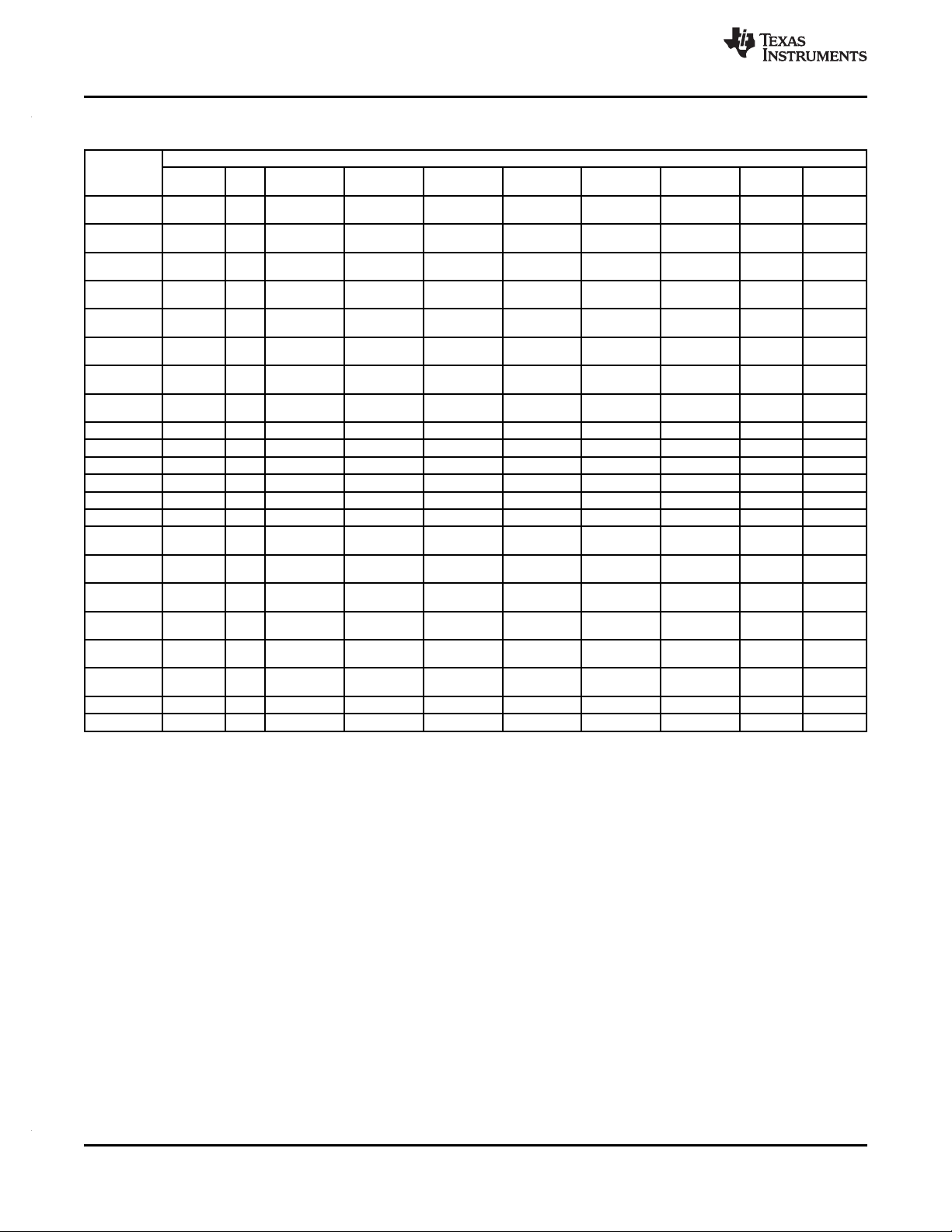
PRODUCTPREVIEW
TMS320C6472
SPRS612E–JUNE 2009–REVISED OCTOBER 2010
www.ti.com
MASTERS
EDMA3 Transfer
Controller0_R
EDMA3 Transfer
Controller0_W
EDMA3 Transfer
Controller1_R
EDMA3 Transfer
Controller1_W
EDMA3 Transfer
Controller2_R
EDMA3 Transfer
Controller2_W
EDMA3 Transfer
Controller3_R
EDMA3 Transfer
Controller3_W
EMAC0 Y Y Y Y Y Y Y Y N N
EMAC1 Y Y Y Y Y Y Y Y N N
UTOPIA Y Y Y Y Y Y Y Y N N
HPI Y Y Y Y Y Y Y Y N N
3x TSIP N Y Y Y Y Y Y Y N N
RapidIO Y Y Y Y Y Y Y Y N N
C64x+
Megamodule0
C64x+
Megamodule1
C64x+
Megamodule2
C64x+
Megamodule3
C64x+
Megamodule4
C64x+
Megamodule5
Xconn1_M N N Y Y Y Y Y Y N N
Xconn2_M N N Y Y Y Y Y Y N N
CFGSCR DDR2 Xconn1_S Xconn2_S
Y Y C C C C C C Y N
Y Y C C C C C C Y N
Y Y C C C C C C N Y
Y Y C C C C C C N Y
Y Y Y Y Y Y Y Y N N
Y Y Y Y Y Y Y Y N N
N Y Y Y Y Y Y Y N N
N Y Y Y Y Y Y Y N N
N Y N C C C C C Y N
N Y C N C C C C Y N
N Y C C N C C C Y N
N Y C C C N C C N Y
N Y C C C C N C N Y
N Y C C C C C N N Y
(1) Y = Direct connection in SCR.
C = Logical connection through Xconn1 or Xconn2 bridges.
N = No physical connection.
Table 4-1. DMA SCR Connection Matrix
SLAVES
C64x+ C64x+ C64x+ C64x+ C64x+ C64x+
Megamodule0 Megamodule1 Megamodule2 Megamodule3 Megamodule4 Megamodule5
(1)
92 System Interconnect Copyright © 2009–2010, Texas Instruments Incorporated
Submit Documentation Feedback
Product Folder Link(s) :TMS320C6472
Page 93

PRODUCTPREVIEW
TMS320C6472
www.ti.com
4.3 Priority Allocation
On the C6472 device, DMA data transfers use a priority-based arbitration. The C64x+ megamodule,
EDMA, TSIP, and SRIO peripherals define their own priorities. The Ethernet and HPI peripherals do not
define their own priorities, while the UTOPIA-PDMA only partially defines its own priority. Priorities for
Ethernet, HPI, and UTOPIA-PDMA transfers should be assigned via the Priority Allocation (PRI_ALLOC)
register (see Figure 4-2). A value of 000b has the highest priority, while 111b has the lowest priority. (For
more information on the default priority values in the C64x+ megamodule, EDMA, TSIP, and SRIO
peripheral registers, see the device-compatible reference guides). TI recommends that these priority
registers be reprogrammed upon initial use.
31 16
Reserved
R-1111 1111 1111 1111
15 14 12 11 8
UTOPIA-
(A)
PDMA
R/W-1 R/W-111 R-1111
7 6 5 3 2 0
Reserved HPI EMAC0
R-11 R/W-111 R/W-111
LEGEND: R/W = Read/Write; R = Read only; -n = value at reset
A. UTOPIA-PDMA has 2 bits of priority in the module. The PRI_ALLOC register supplies only the middle significant bit of the priority for
this module.
EMAC1 Reserved
SPRS612E–JUNE 2009–REVISED OCTOBER 2010
4.4 Configuration Switch Fabric
Figure 4-3 shows the connection between the C64x+ megamodule and the configuration switched central
resource (SCR). The configuration SCR is mainly used by the C64x+ megamodules to access peripheral
registers. The data SCR also has a connection to the configuration SCR which allows masters to access
most peripheral registers. The only registers not accessible by the data SCR through the configuration
SCR are the C64x+ megamodule configuration registers; these can only be accessed by the C64x+
megamodules.
The configuration SCR uses 32-bit configuration buses running at a frequency equal to the CPU frequency
divided by 3.
Figure 4-2. Priority Allocation Register (PRI_ALLOC)
Copyright © 2009–2010, Texas Instruments Incorporated System Interconnect 93
Submit Documentation Feedback
Product Folder Link(s) :TMS320C6472
Page 94

PRODUCTPREVIEW
CPU/3
32-bit
CFGSCR
DMA
SCR
M
32
S
C64x+
Megamodule_0
M
M
M
M
M
M
S
S
S
S
S
S
M
Bridge
32
S
BOOTCtl
S
PSC
S
SMC
S
SMCP x6
S
EMC1
S
EMIC0
32
32
32
32
32
32
S
ETBx6
M
Bridge
32
HPI
S
Timer64x12
S
IIC
S
SEC_CTL
S
EMACMDIO
S
Chip-Level
Registers
S
S
PLLCrtl(1,2,3)
S
GPIO
M
Bridge
32
S
EMAC0
DescMem
S
M
Bridge
32
EMAC1
S
EMAC0
S
3xTSIP
S
S
PDMA
S
UTOPIA
M
Bridge
32
SRIO
S
S
M
Bridge
32
3PTC1
S
3PTC2
S
3PTC3
S
S
3PCC
S
3PTC0
M
C64x+
Megamodule_1
C64x+
Megamodule_2
C64x+
Megamodule_3
C64x+
Megamodule_4
C64x+
Megamodule_5
SCR
CPU/6
EMAC1
DescMem
SRIO
DescMem
SCR
CPU/6
SCR
CPU/3
SCR
CPU/3
SCR
CPU/3
SCR
CPU/3
TMS320C6472
SPRS612E–JUNE 2009–REVISED OCTOBER 2010
www.ti.com
Figure 4-3. Configuration Switched Central Resource
94 System Interconnect Copyright © 2009–2010, Texas Instruments Incorporated
Submit Documentation Feedback
Product Folder Link(s) :TMS320C6472
Page 95

PRODUCTPREVIEW
A registerfile
Datapath1 Datapath2
Bregisterfile
D2
S2
M2
xx
xx
L2
Instructiondecode
M1
xx
xx
L1
S1
D1
16/32-bitinstructiondispatch
Instructionfetch
SPLOOP buffer
64 64
C64x+CPU
256
32
L1Dcache/SRAM
Bandwidthmanagement
Memoryprotection
L1datamemorycontroller
IDMA
256
256
Bandwidthmanagement
L1programmemorycontroller
Memoryprotection
256
Advancedevent
triggering
(AET)
Interrupt
andexception
controller
Powercontrol
L2memory
controller
256
256
MasterDMA
SlaveDMA
128
256
L1P cache/SRAM
L2cache/
SRAM
256
128
128
Toprimary
switchfabric
Cache
control
Bandwidth
management
Memory
protection
Cachecontrol
Cachecontrol
Internal
ROM
256
Configuration
registers
32
ToChip
registers
Externalmemory
controller
www.ti.com
5 C64x+ Megamodule
The C64x+ Megamodule consists of several components — the C64x+ CPU, the L1 program and data
memory controllers, the L2 memory controller, the internal DMA (IDMA), the interrupt controller,
power-down controller, and external memory controller. The C64x+ Megamodule also provides support for
memory protection (for L1P, L1D, and L2 memories) and bandwidth management (for resources local to
the C64x+ Megamodule). Figure 5-1 shows a block diagram of the C64x+ Megamodule.
TMS320C6472
SPRS612E–JUNE 2009–REVISED OCTOBER 2010
5.1 Memory Architecture
Copyright © 2009–2010, Texas Instruments Incorporated C64x+ Megamodule 95
For more detailed information on the TMS320C64x+ megamodule on the C6472 device, see the
TMS320C64x+ DSP Megamodule Reference Guide (literature number SPRU871).
The TMS320C6472 device contains a 608KB level-2 memory (L2), a 32KB level-1 program memory
(L1P), and a 32KB level-1 data memory (L1D).
The L1P memory configuration for the C6472 device is as follows:
• Region 0 size is 0K bytes (disabled).
• Region 1 size is 32K bytes with no wait states.
The L1D memory configuration for the C6472 device is as follows:
• Region 0 size is 0K bytes (disabled).
• Region 1 size is 32K bytes with no wait states.
Figure 5-1. 64x+ Megamodule Block Diagram
Submit Documentation Feedback
Product Folder Link(s) :TMS320C6472
Page 96

PRODUCTPREVIEW
4K bytes
8K bytes
16K bytes
L1P memory
00E0 0000h
00E0 4000h
00E0 6000h
00E0 7000h
00E0 8000h
direct
mapped
SRAM
1/2
dm
3/4
SRAM
SRAM
7/8
All
SRAM
000 001 010 011 100
Block base
address
L1P mode bits
cache
4K bytes
cache
direct
mapped
cache
direct
mapped
cache
4K bytes
8K bytes
16K bytes
L1D memory
00F0 0000h
00F0 4000h
00F0 6000h
00F0 7000h
00F0 8000h
2-way
SRAM
1/2
2-way
3/4
SRAM
SRAM
7/8
All
SRAM
000 001 010 011 100
Block base
address
L1D mode bits
cache
4K bytes
cache
2-way
cache
2-way
cache
TMS320C6472
SPRS612E–JUNE 2009–REVISED OCTOBER 2010
L1D is a two-way set-associative cache while L1P is a direct-mapped cache.
The L1P and L1D cache can be reconfigured via software through the L1PMODE field of the L1P
Configuration Register (L1PCFG) and the L1DMODE field of the L1D Configuration Register (L1DCFG) of
the C64x+ Megamodule. After device reset, L1P and L1D cache are configured as all cache or all SRAM.
The on-chip Bootloader changes the reset configuration for L1P and L1D. For more information, see the
TMS320C645x/C647x Bootloader User's Guide (literature number SPRUEC6).
Figure 5-2 and Figure 5-3 show the available SRAM/cache configurations for L1P and L1D, respectively.
www.ti.com
96 C64x+ Megamodule Copyright © 2009–2010, Texas Instruments Incorporated
Figure 5-2. TMS320C6472 L1P Memory Configurations
Figure 5-3. TMS320C6472 L1D Memory Configurations
Submit Documentation Feedback
Product Folder Link(s) :TMS320C6472
Page 97
PRODUCTPREVIEW
www.ti.com
The L2 memory configuration for the C6472 device is as follows:
• Port 0 configuration:
– Memory size is 608KB
– Starting address is 0080 0000h
– 2-cycle latency
– 4 × 128-bit bank configuration
• Port 1 configuration:
– Memory size 768K ROM, starting address is 0010 0000h
– Memory size is 768KB shared RAM, starting address is 0020 0000h
– 1-cycle latency
– 4 × 256-bit bank configuration
HEX ADDRESS RANGE DESCRIPTION
ROM
0010 0000 - 0010 FFFF Shared Memory Controller Page 0
0011 0000 - 0011 FFFF Shared Memory Controller Page 1
0012 0000 - 0012 FFFF Shared Memory Controller Page 2
0013 0000 - 0013 FFFF Shared Memory Controller Page 3
0014 0000 - 0014 FFFF Shared Memory Controller Page 4
0015 0000 - 0015 FFFF Shared Memory Controller Page 5
0016 0000 - 0016 FFFF Shared Memory Controller Page 6
0017 0000 - 0017 FFFF Shared Memory Controller Page 7
0018 0000 - 0018 FFFF Shared Memory Controller Page 8
0019 0000 - 0019 FFFF Shared Memory Controller Page 9
001A 0000 - 001A FFFF Shared Memory Controller Page 10
001B 0000 - 001B FFFF Shared Memory Controller Page 11
001C 0000 - 001F FFFF Reserved
RAM
0020 0000 - 0020 FFFF Shared Memory Controller Page 16
0021 0000 - 0021 FFFF Shared Memory Controller Page 17
0022 0000 - 0022 FFFF Shared Memory Controller Page 18
0023 0000 - 0023 FFFF Shared Memory Controller Page 19
0024 0000 - 0024 FFFF Shared Memory Controller Page 20
0025 0000 - 0025 FFFF Shared Memory Controller Page 21
0026 0000 - 0026 FFFF Shared Memory Controller Page 22
0027 0000 - 0027 FFFF Shared Memory Controller Page 23
0028 0000 - 0028 FFFF Shared Memory Controller Page 24
0029 0000 - 0029 FFFF Shared Memory Controller Page 25
002A 0000 - 002A FFFF Shared Memory Controller Page 26
002B 0000 - 002B FFFF Shared Memory Controller Page 27
002C 0000 - 002F FFFF Reserved
TMS320C6472
SPRS612E–JUNE 2009–REVISED OCTOBER 2010
Table 5-1. SL2 Prefetch Enabled Memory Regions
Copyright © 2009–2010, Texas Instruments Incorporated C64x+ Megamodule 97
Submit Documentation Feedback
Product Folder Link(s) :TMS320C6472
Page 98
PRODUCTPREVIEW
32Kbytes
32Kbytes
64Kbytes
128Kbytes
352Kbytes
L2memory
00800000h
00858000h
00878000h
00888000h
00890000h
00898000h
11/19
SRAM
4-way
cache
4-way
cache
15/19
SRAM
4-way
cache
17/19
SRAM
4-way
18/19
SRAM
All
SRAM
000 001 010 011 111
Blockbase
address
L2modebits
TMS320C6472
SPRS612E–JUNE 2009–REVISED OCTOBER 2010
L2 memory can be configured as all SRAM or as part 4-way set-associative cache. The amount of L2
memory that is configured as cache is controlled through the L2MODE field of the L2 Configuration
Register (L2CFG) of the C64x+ Megamodule. Figure 5-4 shows the available SRAM/cache configurations
for L2. By default, L2 is configured as all SRAM after device reset.
www.ti.com
For more information on the operation L1 and L2 caches, see the TMS320C64x+ DSP Cache User's
Guide (literature number SPRU862).
All memory on the C6472 has a unique location in the memory map (see Table 2-2, C6472 Memory Map
Summary).
Figure 5-4. TMS320C6472 L2 Memory Configurations
98 C64x+ Megamodule Copyright © 2009–2010, Texas Instruments Incorporated
Submit Documentation Feedback
Product Folder Link(s) :TMS320C6472
Page 99

PRODUCTPREVIEW
www.ti.com
SPRS612E–JUNE 2009–REVISED OCTOBER 2010
5.2 Memory Protection Support
Memory protection allows an operating system to define who or what is authorized to access L1D, L1P,
and L2 memory. To accomplish this, the L1D, L1P, and L2 memories are divided into pages. There are 16
pages of L1P (2KB each), 16 pages of L1D (2KB each), and up to 64 pages of L2. The L1D, L1P, and L2
memory controllers in the C64x+ Megamodule are equipped with a set of registers that specify the
permissions for each memory page. For L2, the number of protection pages and their sizes depend on the
L2 configuration of the device, as defined in the previous section. The actual sizes are listed in Table 5-2.
Table 5-2 shows the memory addresses used to access the L2 memory.
Table 5-2. L2 Memory Protection Page Sizes
L2
ADDRESS
Shared L2
0020 0000h - 64 KB 64 KB 64 KB 64 KB 64 KB 64 KB
002B FFFFh
002C 0000h - N/A N/A N/A N/A N/A N/A
002F FFFFh
Local L2
0080 0000h - 32 KB 32 KB 32 KB 32 KB 32 KB 32 KB
0089 7FFFh
0089 8000h - N/A N/A N/A N/A N/A N/A
008F FFFFh
C64x+ C64x+ C64x+ C64x+ C64x+ C64x+
MEGAMODULE MEGAMODULE MEGAMODULE MEGAMODULE MEGAMODULE MEGAMODULE
CORE 0 CORE 1 CORE 2 CORE 3 CORE 4 CORE 5
TMS320C6472
Each page may be assigned with fully orthogonal user and supervisor read, write, and execute
permissions. Additionally, a page may be marked as either (or both) locally or globally accessible. A local
access is a direct CPU access to L1D, L1P, and L2, while a global access is initiated by a DMA (either
IDMA or the EDMA3) or by other system masters.
The assignment of privilege IDs for CPU 0 and all non-EDMA system masters is based on silicon revision.
For silicon revisions ≤1.2, CPU 0 and all non-EDMA system masters on the device are assigned the same
privilege ID of 0. For silicon revsions >1.2, CPU 0 is assigned the privilege ID of 6 and all non-EDMA
system masters are assigned the same privilege ID of 0. CPUs 1-5 are each assigned a unique privilege
ID (see Table 5-3). It is only possible to specify whether the memory pages are locally or globally
accessible. The AIDx (x=0,1,2,3,4,5, or X) and LOCAL bits of the memory protection page attribute
registers specify the memory page protection scheme as listed in Table 5-4.
Whenever the CPU is the initiator of a memory transaction, the privilege mode (user or supervisor) in
which the CPU is running at that time is carried with those transactions. This includes EDMA3 transfers
that are programmed by the CPU. For most peripheral masters (EMAC0, EMAC1, UTOPIA, TSIP0, TSIP1,
and TSIP2), the privilege mode is always user mode. Two peripherals (HPI and SRIO) have
programmable privilege modes through a chip-level register, HOSTPRIV, and can be either user or
supervisor.
Table 5-3. Available Memory Page Protection Scheme with Privilege ID
PRIVID MODULE MEMORY PROTECTION PAGE PRIVILEGE MODE DESCRIPTION
0 (Core 0, AID0 Inherited from CPU
silicon revisions ≤1.2)
0 (not SRIO or HPI or Core 0) AID0 User All peripheral masters except
0 (SRIO or HPI) AID0 User/Supervisor (configured in SRIO and HPI
(1) Also applies to EDMA transfers that are programmed by the CPU.
Copyright © 2009–2010, Texas Instruments Incorporated C64x+ Megamodule 99
CORRESPONDING FIELD IN
ATTRIBUTE REGISTERS
Submit Documentation Feedback
Product Folder Link(s) :TMS320C6472
HOSTPRIV)
(1)
C64x+ Megamodule Core 0
SRIO and HPI
Page 100

PRODUCTPREVIEW
TMS320C6472
SPRS612E–JUNE 2009–REVISED OCTOBER 2010
Table 5-3. Available Memory Page Protection Scheme with Privilege ID (continued)
PRIVID MODULE MEMORY PROTECTION PAGE PRIVILEGE MODE DESCRIPTION
1 AID1 Inherited from CPU
2 AID2 Inherited from CPU
3 AID3 Inherited from CPU
4 AID4 Inherited from CPU
5 AID5 Inherited from CPU
6 (Core 0, AIDX Reserved Reserved
silicon revisions ≤1.2)
6 (Core 0, AIDX Inherited from CPU
silicon revisions >1.2)
>6 AIDX Reserved Reserved
Table 5-4. Available Memory Page Protection Scheme with AIDx and Local Bits
PRIVID MODULE LOCAL BIT DESCRIPTION
0 0 No access to memory page is permitted.
0 1 Only direct access by CPU is permitted.
1 0 Only accesses by system masters and IDMA are permitted (includes EDMA and IDMA
1 1 All accesses permitted
CORRESPONDING FIELD IN
ATTRIBUTE REGISTERS
(1)
(1)
(1)
(1)
(1)
(1)
accesses initiated by the CPU).
www.ti.com
C64x+ Megamodule Core 1
C64x+ Megamodule Core 2
C64x+ Megamodule Core 3
C64x+ Megamodule Core 4
C64x+ Megamodule Core 5
C64x+ Megamodule Core 0
Megamodule interrupt controller) service routine. A CPU or DMA access to a page without the proper
permissions will:
• Block the access - reads return zero, writes are voided.
• Capture the initiator in a status register - ID, address, and access type are stored.
• Signal event to CPU interrupt controller.
The software is responsible for taking corrective action to respond to the event and resetting the error
status in the memory controller.
For more information on memory protection for L1D, L1P, and L2, see the TMS320C64x+ DSP
Megamodule Reference Guide (literature number SPRU871).
5.3 Bandwidth Management
When multiple requestors contend for a single C64x+ Megamodule resource, the conflict is solved by
granting access to the highest priority requestor. The following four resources are managed by the
Bandwidth Management control hardware:
• Level 1 Program (L1P) SRAM/Cache
• Level 1 Data (L1D) SRAM/Cache
• Level 2 (L2) SRAM/Cache
• Memory-mapped registers configuration bus
The priority level for operations initiated within the C64x+ Megamodule; e.g., CPU-initiated transfers,
user-programmed cache coherency operations, and IDMA-initiated transfers, are declared through
registers in the C64x+ Megamodule. The priority level for operations initiated outside the C64x+
Megamodule by system peripherals is declared through the Priority Allocation Register (PRI_ALLOC), see
Figure 4-2. System peripherals with no fields in PRI_ALLOC have their own registers to program their
priorities.
Faults are handled by software in an interrupt (or exception, programmable within each C64x+
More information on the bandwidth management features of the C64x+ Megamodule can be found in the
TMS320C64x+ DSP Megamodule Reference Guide (literature number SPRU871).
100 C64x+ Megamodule Copyright © 2009–2010, Texas Instruments Incorporated
Submit Documentation Feedback
Product Folder Link(s) :TMS320C6472
 Loading...