

Page 1

TMS320C6454
www.ti.com
Fixed-Point Digital Signal Processor
Check for Samples: TMS320C6454
1 Features
12
• High-Performance Fixed-Point DSP (C6454)
– 1.39-, 1.17-, and 1-ns Instruction Cycle Time
– 720-MHz, 850-MHz, and 1-GHz Clock Rate
– Eight 32-Bit Instructions/Cycle
– 8000 MIPS/MMACS (16-Bits)
– Commercial Temperature [0°C to 90°C]
– Extended Temperature [-40°C to 105°C]
• TMS320C64x+™ DSP Core
– Dedicated SPLOOP Instruction
– Compact Instructions (16-Bit)
– Instruction Set Enhancements
– Exception Handling
• TMS320C64x+ Megamodule L1/L2 Memory
Architecture:
– 256K-Bit (32K-Byte) L1P Program Cache
[Direct Mapped]
– 256K-Bit (32K-Byte) L1D Data Cache
[2-Way Set-Associative]
– 8M-Bit (1048K-Byte) L2 Unified Mapped
RAM/Cache [Flexible Allocation]
– 256K-Bit (32K-Byte) L2 ROM
– Time Stamp Counter
• Endianess: Little Endian, Big Endian
• 64-Bit External Memory Interface (EMIFA)
– Glueless Interface to Asynchronous
Memories (SRAM, Flash, and EEPROM) and
Synchronous Memories (SBSRAM, ZBT
SRAM)
– Supports Interface to Standard Sync
Devices and Custom Logic (FPGA, CPLD,
ASICs, etc.)
– 32M-Byte Total Addressable External
Memory Space
• DDR2 Memory Controller
– Interfaces to DDR2-533 SDRAM
– 32-Bit/16-Bit, 533-MHz (data rate) Bus
– 512M-Byte Total Addressable External
SPRS311F–APRIL 2006–REVISED SEPTEMBER 2010
TMS320C6454
Memory Space
• EDMA3 Controller (64 Independent Channels)
• 32-/16-Bit Host-Port Interface (HPI)
• 32-Bit 33-/66-MHz, 3.3-V Peripheral Component
Interconnect (PCI) Master/Slave Interface
Conforms to PCI Local Bus Specification (v2.3)
• One Inter-Integrated Circuit (I2C) Bus
• Two McBSPs
• 10/100/1000 Mb/s Ethernet MAC (EMAC)
– IEEE 802.3 Compliant
– Supports Multiple Media Independent
Interfaces (MII, GMII, RMII, and RGMII)
– 8 Independent Transmit (TX) and
8 Independent Receive (RX) Channels
• Two 64-Bit General-Purpose Timers,
Configurable as Four 32-Bit Timers
• 16 General-Purpose I/O (GPIO) Pins
• System PLL and PLL Controller
• Secondary PLL and PLL Controller, Dedicated
to EMAC and DDR2 Memory Controller
• Advanced Event Triggering (AET) Compatible
• Trace-Enabled Device
• IEEE-1149.1 (JTAG™)
Boundary-Scan-Compatible
• 697-Pin Ball Grid Array (BGA) Package
(ZTZ or GTZ Suffix), 0.8-mm Ball Pitch
• 0.09-mm/7-Level Cu Metal Process (CMOS)
• 3.3-/1.8-/1.5-V I/Os,
1.25-/1.2-V Internal
• Pin-Compatible with the TMS320C6455
Fixed-Point Digital Signal Processor
1
Please be aware that an important notice concerning availability, standard warranty, and use in critical applications of Texas
Instruments semiconductor products and disclaimers thereto appears at the end of this data sheet.
2All trademarks are the property of their respective owners.
PRODUCTION DATA information is current as of publication date.
Products conform to specifications per the terms of the Texas
Instruments standard warranty. Production processing does not
necessarily include testingof all parameters.
Copyright © 2006–2010, Texas Instruments Incorporated
Page 2
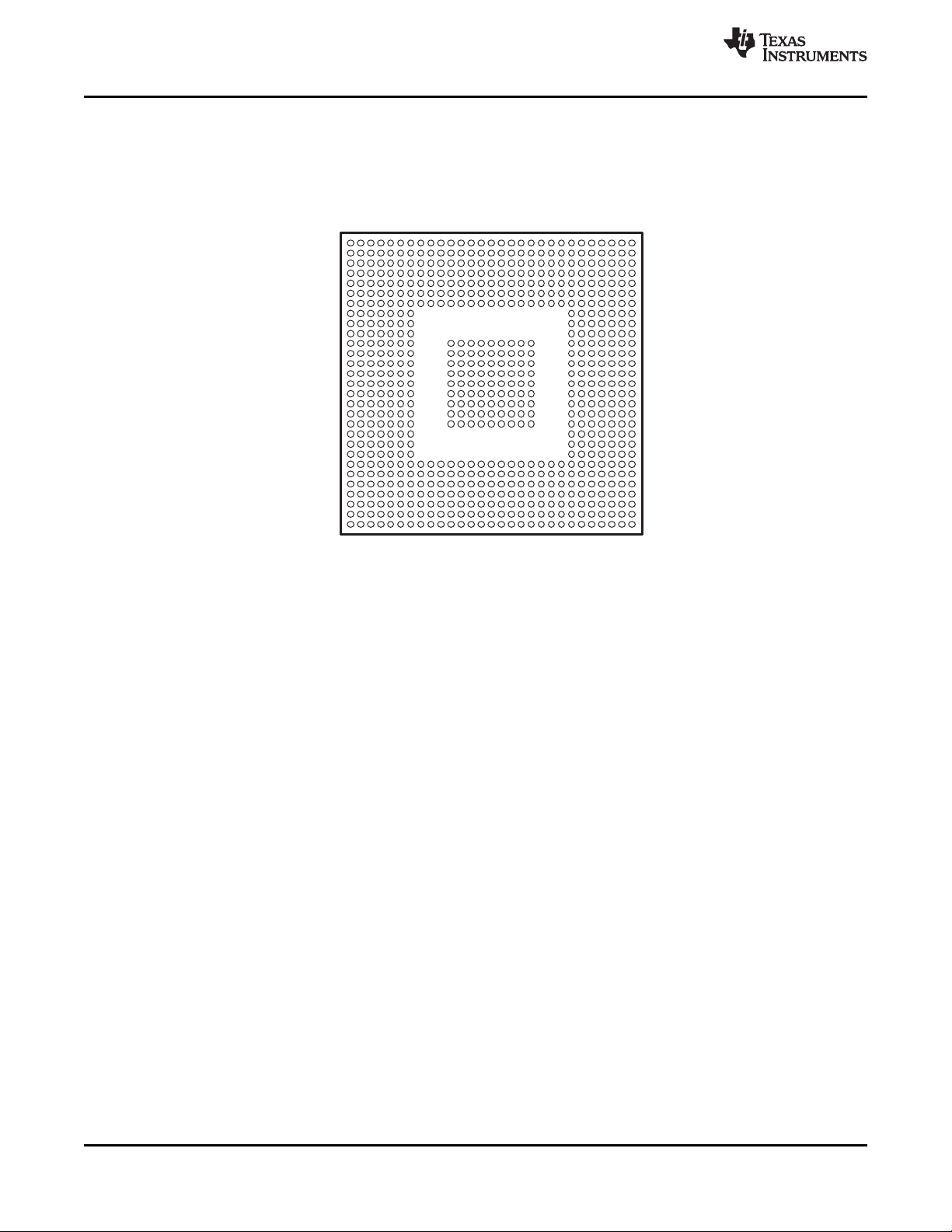
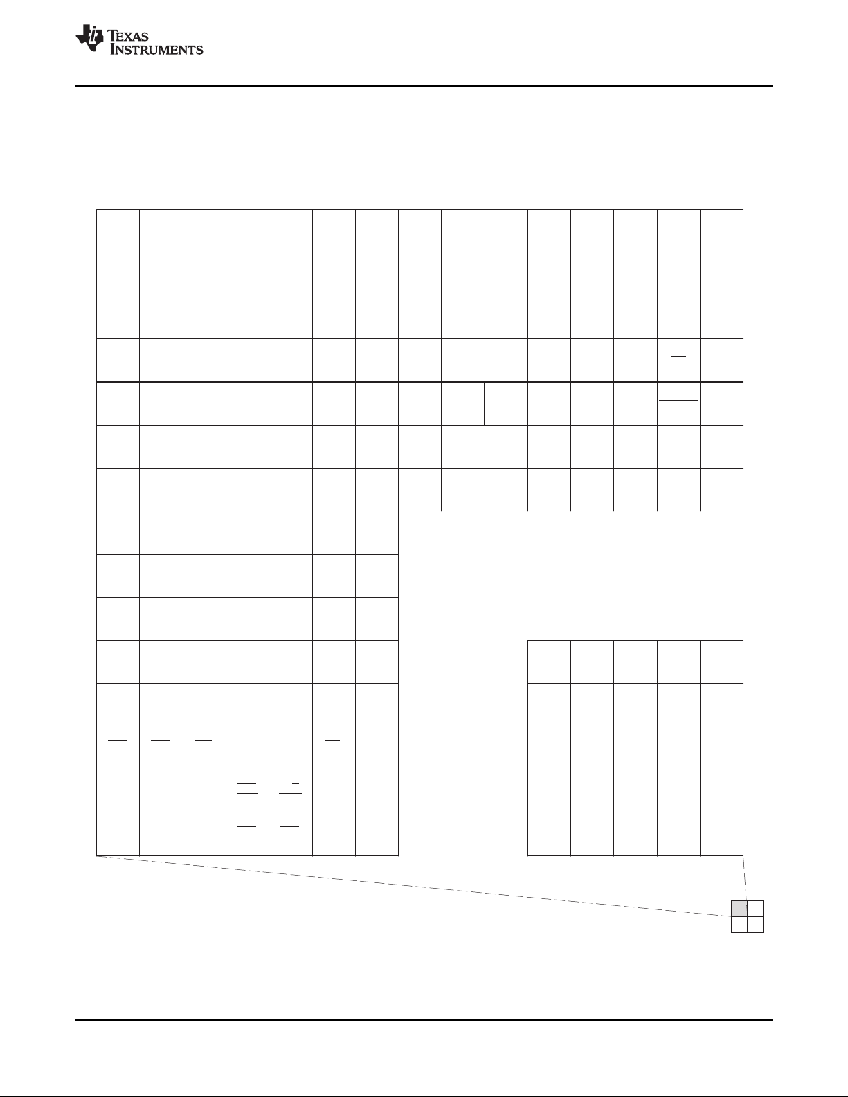
ZTZ/GTZ 697-PIN BALL GRID ARRAY (BGA) PACKAGE
(BOTTOM VIEW)
A
2
B
1
345678910111213141516171819202122232425
26
C
D
E
F
G
H
J
K
L
M
N
P
R
T
U
V
W
Y
AA
AB
AC
AD
AE
AF
272829
AG
AH
AJ
NOTE: The ZTZ mechanical package designator represents the version of the GTZ package with lead-free balls. For more detailed information,
see the Mechanical Data section of this document.
TMS320C6454
SPRS311F–APRIL 2006–REVISED SEPTEMBER 2010
1.1 ZTZ/GTZ BGA Package (Bottom View)
Figure 1-1 shows the TMS320C6454 device 697-pin ball grid array package (bottom view).
www.ti.com
Figure 1-1. ZTZ/GTZ BGA Package (Bottom View)
1.2 Description
The TMS320C64x+™ DSPs (including the TMS320C6454 device) are the highest-performance fixed-point
DSP generation in the TMS320C6000™ DSP platform. The C6454 device is based on the third-generation
high-performance, advanced VelociTI™ very-long-instruction-word (VLIW) architecture developed by
Texas Instruments (TI), making these DSPs an excellent choice for applications including video and
telecom infrastructure, imaging/medical, and wireless infrastructure (WI). The C64x+™ devices are
upward code-compatible from previous devices that are part of the C6000™ DSP platform.
The C6454 device offers a lower cost pin-compatible migration path for C6455 customers who don't need
the 2MB of the C6455 or the high-speed interconnect provided by Serial RapidIO. The C6454 device also
provides an excellent migration path for existing C6414/6415/6416 customers who require C6454
advanced peripherals; DDR2 at 533 MHz provides 2x performance boost over older SDRAM interface,
gigabit Ethernet provides low-cost high-performance ubiquitous packet interface, and 66-MHz PCI
(revision 2.3 complaint) provides legacy high-bandwidth interconnect.
Based on 90-nm process technology and with performance of up to 8000 million instructions per second
(MIPS) [or 8000 16-bit MMACs per cycle] at a 1-GHz clock rate, the C6454 device offers cost-effective
solutions to high-performance DSP programming challenges. The C6454 DSP possesses the operational
flexibility of high-speed controllers and the numerical capability of array processors.
The C64x+ DSP core employs eight functional units, two register files, and two data paths. Like the earlier
C6000 devices, two of these eight functional units are multipliers or .M units. Each C64x+ .M unit doubles
the multiply throughput versus the C64x core by performing four 16-bit x 16-bit multiply-accumulates
(MACs) every clock cycle. Thus, eight 16-bit x 16-bit MACs can be executed every cycle on the C64x+
core. At a 1-GHz clock rate, this means 8000 16-bit MMACs can occur every second. Moreover, each
multiplier on the C64x+ core can compute one 32-bit x 32-bit MAC or four 8-bit x 8-bit MACs every clock
cycle.
2 Features Copyright © 2006–2010, Texas Instruments Incorporated
Submit Documentation Feedback
Product Folder Link(s): TMS320C6454
Page 3

TMS320C6454
www.ti.com
The C6454 DSP integrates a large amount of on-chip memory organized as a two-level memory system.
The level-1 (L1) program and data memories on the C6454 device are 32KB each. This memory can be
configured as mapped RAM, cache, or some combination of the two. When configured as cache, L1
program (L1P) is a direct mapped cache where as L1 data (L1D) is a two-way set associative cache. The
level-2 (L2) memory is shared between program and data space and is 1048KB in size. L2 memory can
also be configured as mapped RAM, cache, or some combination of the two. The C64x+ Megamodule
also has a 32-bit peripheral configuration (CFG) port, an internal DMA (IDMA) controller, a system
component with reset/boot control, interrupt/exception control, a power-down control, and a free-running
32-bit timer for time stamp.
The peripheral set includes: an inter-integrated circuit bus module (I2C); two multichannel buffered serial
ports (McBSPs); a user-configurable 16-bit or 32-bit host-port interface (HPI16/HPI32); a peripheral
component interconnect (PCI); a 16-pin general-purpose input/output port (GPIO) with programmable
interrupt/event generation modes; an 10/100/1000 Ethernet media access controller (EMAC), which
provides an efficient interface between the C6454 DSP core processor and the network; a management
data input/output (MDIO) module (also part of the EMAC) that continuously polls all 32 MDIO addresses in
order to enumerate all PHY devices in the system; a glueless external memory interface (64-bit EMIFA),
which is capable of interfacing to synchronous and asynchronous peripherals; and a 32-bit DDR2 SDRAM
interface.
The I2C ports on the C6454 device allows the DSP to easily control peripheral devices and communicate
with a host processor. In addition, the standard multichannel buffered serial port (McBSP) may be used to
communicate with serial peripheral interface (SPI) mode peripheral devices.
SPRS311F–APRIL 2006–REVISED SEPTEMBER 2010
The C6454 DSP has a complete set of development tools which includes: a new C compiler, an assembly
optimizer to simplify programming and scheduling, and a Windows® debugger interface for visibility into
source code execution.
Copyright © 2006–2010, Texas Instruments Incorporated Features 3
Submit Documentation Feedback
Product Folder Link(s): TMS320C6454
Page 4
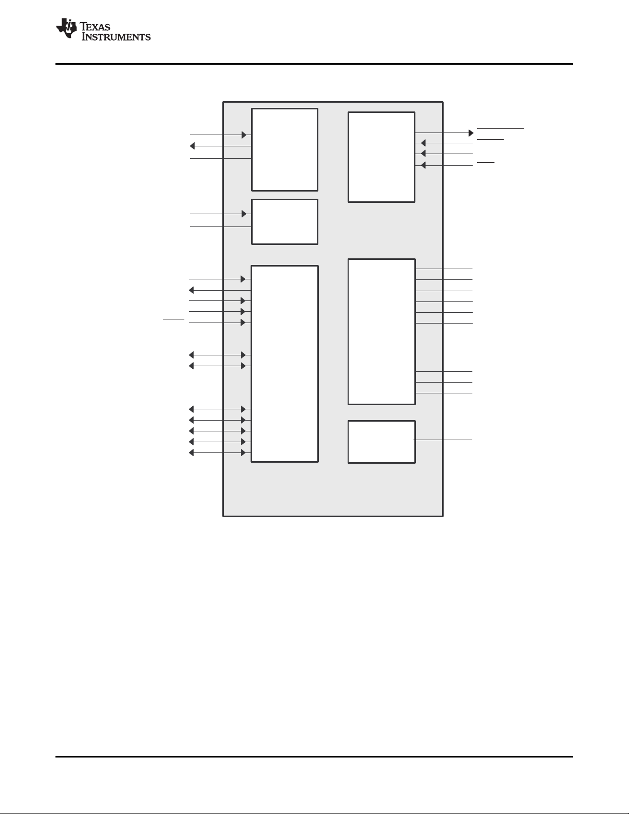
MDIO
EMAC
10/100/1000
Serial
RapidIO
DDR2
Mem Ctlr
64
C6454
HI
I2C
16
RMGII
(D)
L2
Cache
Memory
1048K
Bytes
HPI (32/16)
(B)
DDR2 SDRAM
32
LO
Timer1
(C)
PLL2 and
PLL2
Controller
(D)
GMII
RMII
MII
Primary
Switched
Central
Resource
L2 Memory Controller
(Memory Protect/
Bandwidth Mgmt)
System
C64x+ DSP Core
Data Path B
B Register File
B31−B16
B15−B0
Instruction Fetch
Data Path A
A Register File
A31−A16
A15−A0
.L1
.S1
.M1
xxxx.D1 .D2
.M2
xx
xx
.S2
.L2
Internal DMA
(IDMA)
M
e
g
a
m
o
d
u
l
e
L1P Memory Controller (Memory Protect/Bandwidth Mgmt)
Instruction
Decode
16-/32-bit
Instruction Dispatch
Power Control
L1D Memory Controller (Memory Protect/Bandwidth Mgmt)
Interrupt and Exception Controller
EMIFA
HI
LO
Timer1
(C)
EDMA 3.0
Secondary
Switched Central
Resource
PLL1 and
PLL1
Controller
Device
Configuration
Logic
Boot Configuration
L1D SRAM/Cache
2-Way Set-Associative
32K Bytes Total
L1P SRAM/Cache Direct-Mapped
32K Bytes
L2 ROM
32K
Bytes
(E)
Control Registers
SPLOOP Buffer
In-Circuit Emulation
PCI66
(B)
GPIO16
(B)
McBSP1
(A)
McBSP0
(A)
SBSRAM
ZBT SRAM
SRAM
ROM/FLASH
I/O Devices
TMS320C6454
SPRS311F–APRIL 2006–REVISED SEPTEMBER 2010
www.ti.com
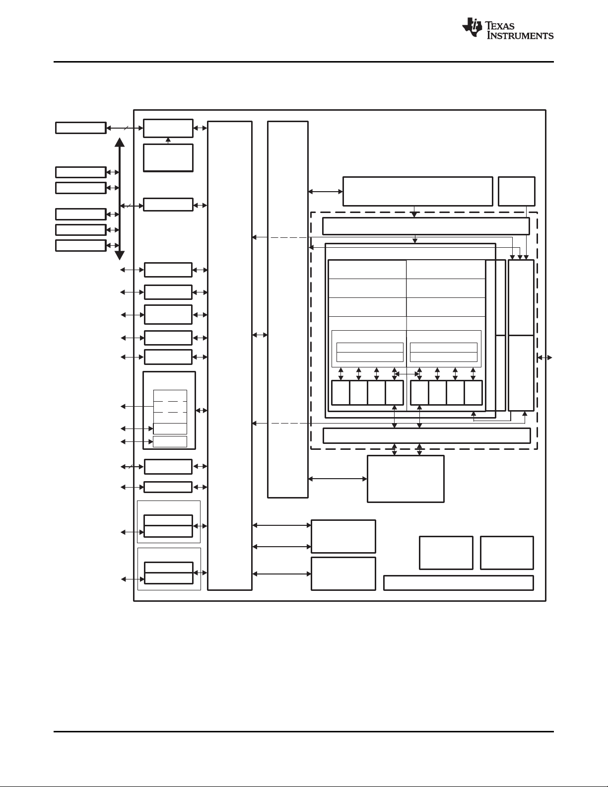
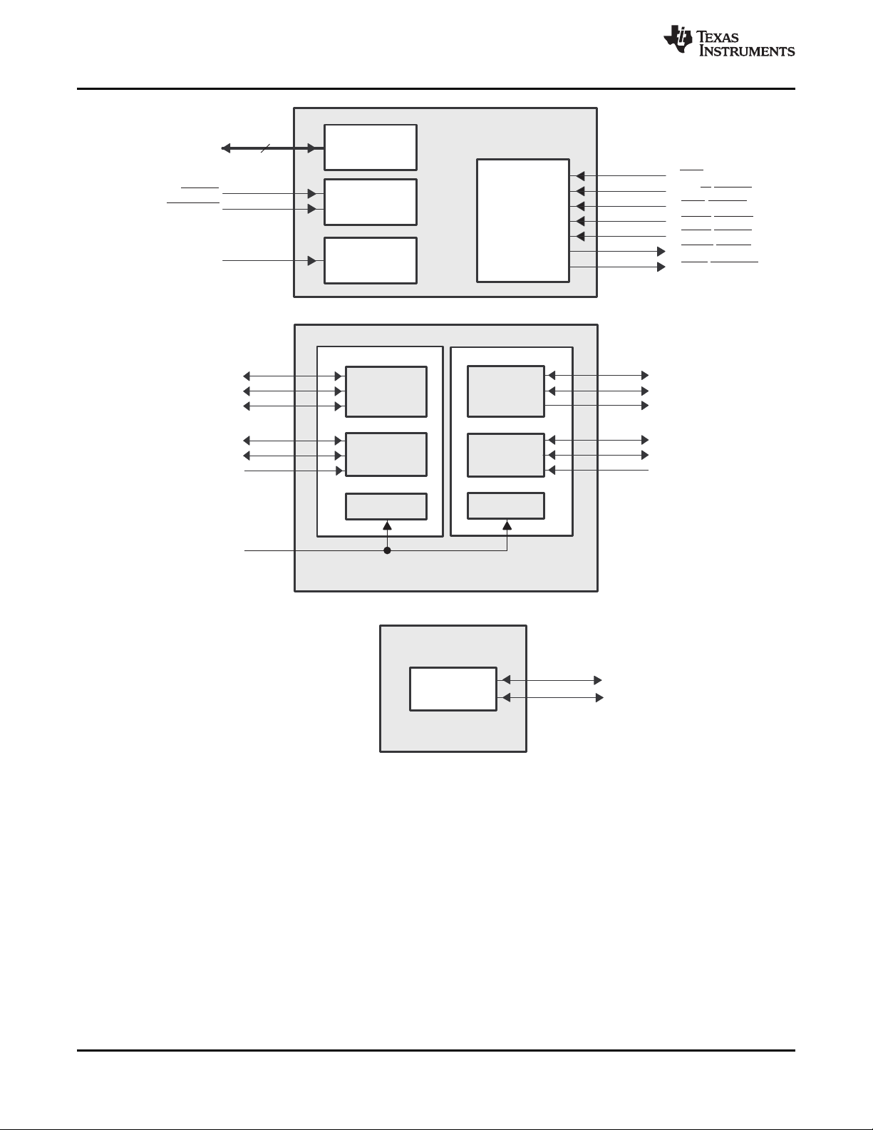
1.3 Functional Block Diagram
Figure 1-2 shows the functional block diagram of the C6454 device.
4 Features Copyright © 2006–2010, Texas Instruments Incorporated
Figure 1-2. Functional Block Diagram
Submit Documentation Feedback
Product Folder Link(s): TMS320C6454
A. McBSPs: Framing Chips - H.100, MVIP, SCSA, T1, E1; AC97 Devices; SPI Devices; Codecs.
B. The PCI peripheral pins are muxed with some of the HPI peripheral pins . For more detailed information, see
Section 3, Device Configuration.
C. Each of the TIMER peripherals (TIMER1 and TIMER0) is configurable as a 64-bit general-purpose timer, dual 32-bit
general-purpose timers, or a watchdog timer.
D. The PLL2 controller also generates clocks for the EMAC.
E. When accessing the internal ROM of the DSP, the CPU frequency must always be less than 750 MHz.
Page 5

TMS320C6454
www.ti.com
1 Features ................................................... 1
1.1 ZTZ/GTZ BGA Package (Bottom View) ............. 2
1.2 Description ........................................... 2
1.3 Functional Block Diagram ............................ 4
5.4 Power-Down Control ............................... 83
5.5 Megamodule Resets ................................ 83
5.6 Megamodule Revision .............................. 84
5.7 C64x+ Megamodule Register Descriptions ......... 85
SPRS311F–APRIL 2006–REVISED SEPTEMBER 2010
Revision History .............................................. 6 6 Device Operating Conditions ....................... 93
2 Device Overview ........................................ 7
2.1 Device Characteristics ............................... 7
2.2 CPU (DSP Core) Description ........................ 8
2.3 Memory Map Summary ............................. 11
2.4 Boot Sequence ..................................... 13
2.5 Pin Assignments .................................... 15
2.6 Signal Groups Description .......................... 19
2.7 Terminal Functions ................................. 24
2.8 Development ........................................ 48
3 Device Configuration ................................. 52
3.1 Device Configuration at Device Reset .............. 52
3.2 Peripheral Configuration at Device Reset .......... 54
3.3 Peripheral Selection After Device Reset ........... 55
3.4 Device State Control Registers ..................... 57
3.5 Device Status Register Description ................ 67
3.6 JTAG ID (JTAGID) Register Description ........... 69
3.7 Pullup/Pulldown Resistors .......................... 70
3.8 Configuration Examples ............................ 70
4 System Interconnect .................................. 73
4.1 Internal Buses, Bridges, and Switch Fabrics ....... 73
4.2 Data Switch Fabric Connections ................... 74
4.3 Configuration Switch Fabric ........................ 76
4.4 Bus Priorities ....................................... 77
5 C64x+ Megamodule ................................... 79
5.1 Memory Architecture ............................... 79
5.2 Memory Protection ................................. 81
5.3 Bandwidth Management ............................ 82
6.1 Absolute Maximum Ratings Over Operating Case
Temperature Range (Unless Otherwise Noted) .... 93
6.2 Recommended Operating Conditions .............. 93
6.3 Electrical Characteristics Over Recommended
Ranges of Supply Voltage and Operating Case
Temperature (Unless Otherwise Noted) ............ 95
7 C64x+ Peripheral Information and Electrical
Specifications .......................................... 97
7.1 Parameter Information .............................. 97
7.2 Recommended Clock and Control Signal Transition
Behavior ............................................ 98
7.3 Power Supplies ..................................... 99
7.4 Enhanced Direct Memory Access (EDMA3)
Controller .......................................... 101
7.5 Interrupts .......................................... 116
7.6 Reset Controller ................................... 120
7.7 PLL1 and PLL1 Controller ......................... 128
7.8 PLL2 and PLL2 Controller ......................... 143
7.9 DDR2 Memory Controller ......................... 152
7.10 External Memory Interface A (EMIFA) ............ 154
7.11 I2C Peripheral ..................................... 165
7.12 Host-Port Interface (HPI) Peripheral .............. 170
7.13 Multichannel Buffered Serial Port (McBSP) ....... 181
7.14 Ethernet MAC (EMAC) ............................ 195
7.15 Timers ............................................. 213
7.16 Peripheral Component Interconnect (PCI) ........ 215
7.17 General-Purpose Input/Output (GPIO) ............ 222
7.18 Emulation Features and Capability ............... 224
8 Mechanical Data ...................................... 226
8.1 Thermal Data ...................................... 226
8.2 Packaging Information ............................ 226
Copyright © 2006–2010, Texas Instruments Incorporated Contents 5
Submit Documentation Feedback
Product Folder Link(s): TMS320C6454
Page 6

TMS320C6454
SPRS311F–APRIL 2006–REVISED SEPTEMBER 2010
NOTE: Page numbers for previous revisions may differ from page numbers in the current version.
This data manual revision history highlights the technical changes made to the document in this revision.
Scope: Applicable updates to the C64x device family, specifically relating to the TMS320C6454 device,
have been incorporated.
SEE ADDITIONS/MODIFICATIONS/DELETIONS
Table 3-1 C6454 Device Configuration Pins (AEA[19:0], ABA[1:0], and PCI_EN):
Modified Configuration Pin AEA11 Functional Description
Section 7.7 PLL1 and PLL1 Controller:
Modified Figure 7-10, PLL1 and PLL1 Controller
Table 7-71 Ethernet MAC (EMAC) Control Registers:
Corrected Hex Address Range for Registers RXINTSTATRAW - MACINTMASKCLEAR
Section 7.14.3.2 EMAC RMII Electrical Data/Timing:
Corrected signal names in Table 7-82, Switching Characteristics Over Recommended Operating Conditions
for EMAC RMII Transmit 10/100 Mbit/s, Figure 7-66, EMAC Transmit Interface Timing [RMII Operation],
Table 7-83, Timing Requirements for EMAC RMII Input Receive for 100 Mbps, and Figure 7-67, EMAC
Receive Interface Timing [RMII Operation]
Section 7.14.3.3 EMAC RGMII Electrical Data/Timing:
Corrected signal names in Table 7-85, Timing Requirements for RGRXC - RGMII Operation, Table 7-86,
Timing Requirements for EMAC RGMII Input Receive for 10/100/1000 Mbps, Figure 7-69, EMAC Receive
Interface Timing [RGMII Operation], Table 7-87, Switching Characteristics Over Recommended Operating
Conditions for RGTXC - RGMII Operation for 10/100/1000 Mbit/s, Table 7-88, Switching Characteristics Over
Recommended Operating Conditions for EMAC RGMII Transmit, and Figure 7-70, EMAC Transmit Interface
Timing [RGMII Operation]
www.ti.com
Revision History
C6454 DSP Revision History
6 Contents Copyright © 2006–2010, Texas Instruments Incorporated
Submit Documentation Feedback
Product Folder Link(s): TMS320C6454
Page 7
TMS320C6454
www.ti.com
SPRS311F–APRIL 2006–REVISED SEPTEMBER 2010
2 Device Overview
2.1 Device Characteristics
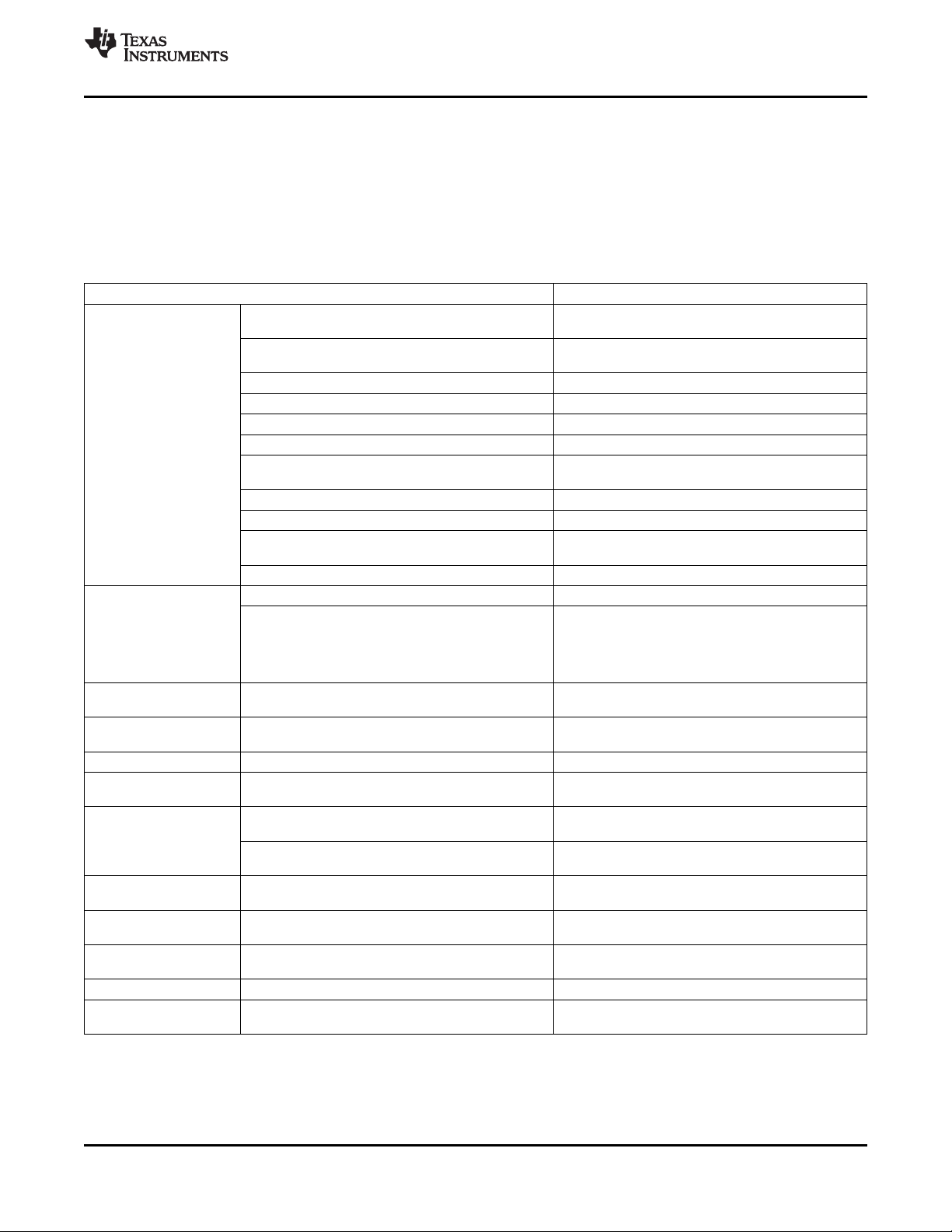
Table 2-1, provides an overview of the C6454 DSP. The tables show significant features of the C6454
device, including the capacity of on-chip RAM, the peripherals, the CPU frequency, and the package type
with pin count.
Table 2-1. Characteristics of the C6454 Processor
HARDWARE FEATURES C6454
EMIFA (64-bit bus width)
(clock source = AECLKIN or SYSCLK4)
DDR2 Memory Controller (32-bit bus width) [1.8 V I/O]
(clock source = CLKIN2)
EDMA3 (64 independent channels) [CPU/3 clock rate] 1
Peripherals
Not all peripherals pins
are available at the same
time (For more detail, see
Section 3, Device
Configuration).
On-Chip Memory
C64x+ Megamodule Megamodule Revision ID Register (address location:
Revision ID 0181 2000h)
JTAG BSDL_ID JTAGID register (address location: 0x02A80008)
Frequency MHz 720, 850, and 1000 (1 GHz)
Cycle Time ns
Voltage
PLL1 and PLL1
Controller Options
PLL2 x20
BGA Package 24 x 24 mm
Process Technology mm 0.09 mm
Product Status
(2)
I2C 1
HPI (32- or 16-bit user selectable) 1 (HPI16 or HPI32)
PCI (32-bit), [66-MHz or 33-MHz] 1 (PCI66 or PCI33)
McBSPs (internal CPU/6 or external clock source up
to 100 Mbps)
10/100/1000 Ethernet MAC (EMAC) 1
Management Data Input/Output (MDIO) 1
64-Bit Timers (Configurable)
(internal clock source = CPU/6 clock frequency)
General-Purpose Input/Output Port (GPIO) 16
Size (Bytes) 1144K
32K-Byte (32KB) L1 Program Memory Controller
Organization 32KB Data Memory Controller [SRAM/Cache]
See Section 5.6, Megamodule Revision
See Section 3.6, JTAG ID (JTAGID) Register
1.39 ns (C6454-720), 1.17 ns (C6454-850),
1 ns (C6454 A-1000, -1000) [1-GHz CPU]
Core (V)
I/O (V)
CLKIN1 frequency multiplier Bypass (x1), x15, x20, x25, x30, x32
CLKIN2 frequency multiplier
[DDR2 Memory Controller and EMAC support only]
697-Pin Flip-Chip Plastic BGA (ZTZ)
Product Preview (PP), Advance Information (AI),
or Production Data (PD)
2 64-bit or 4 32-bit
1024KB L2 Unified Memory/Cache
1.25 V (A-1000/-1000)
1.5/1.8 [EMAC RGMII], and
1.8 and 3.3 V [I/O Supply Voltage]
697-Pin Plastic BGA (GTZ)
1
1
2
[SRAM/Cache]
32KB L2 ROM
Description
1.2 V (-850/-720)
PD
(1)
(1) The extended temperature device's (A-1000) electrical characteristics and ac timings are the same as those for the corresponding
commercial temperature devices (-1000).
(2) PRODUCTION DATA information is current as of publication date. Products conform to specifications per the terms of Texas
Instruments standard warranty. Production processing does not necessarily include testing of all parameters.
Copyright © 2006–2010, Texas Instruments Incorporated Device Overview 7
Submit Documentation Feedback
Product Folder Link(s): TMS320C6454
Page 8

TMS320C6454
SPRS311F–APRIL 2006–REVISED SEPTEMBER 2010
www.ti.com
Table 2-1. Characteristics of the C6454 Processor (continued)
HARDWARE FEATURES C6454
Device Part Numbers TMS320C6454ZTZ8 , TMS320C6454GTZ8
(For more details on the C64x+™ DSP part
numbering, see Figure 2-12)
TMS320C6454ZTZ7, TMS320C6454GTZ7
TMS320C6454ZTZ , TMS320C6454GTZ
2.2 CPU (DSP Core) Description
The C64x+ Central Processing Unit (CPU) consists of eight functional units, two register files, and two
data paths as shown in Figure 2-1. The two general-purpose register files (A and B) each contain
32 32-bit registers for a total of 64 registers. The general-purpose registers can be used for data or can be
data address pointers. The data types supported include packed 8-bit data, packed 16-bit data, 32-bit
data, 40-bit data, and 64-bit data. Values larger than 32 bits, such as 40-bit-long or 64-bit-long values are
stored in register pairs, with the 32 LSBs of data placed in an even register and the remaining 8 or
32 MSBs in the next upper register (which is always an odd-numbered register).
The eight functional units (.M1, .L1, .D1, .S1, .M2, .L2, .D2, and .S2) are each capable of executing one
instruction every clock cycle. The .M functional units perform all multiply operations. The .S and .L units
perform a general set of arithmetic, logical, and branch functions. The .D units primarily load data from
memory to the register file and store results from the register file into memory.
The C64x+ CPU extends the performance of the C64x core through enhancements and new features.
Each C64x+ .M unit can perform one of the following each clock cycle: one 32 x 32 bit multiply, two
16 x 16 bit multiplies, two 16 x 32 bit multiplies, four 8 x 8 bit multiplies, four 8 x 8 bit multiplies with add
operations, and four 16 x 16 multiplies with add/subtract capabilities (including a complex multiply). There
is also support for Galois field multiplication for 8-bit and 32-bit data. Many communications algorithms
such as FFTs and modems require complex multiplication. The complex multiply (CMPY) instruction takes
for 16-bit inputs and produces a 32-bit real and a 32-bit imaginary output. There are also complex
multiplies with rounding capability that produces one 32-bit packed output that contain 16-bit real and
16-bit imaginary values. The 32 x 32 bit multiply instructions provide the extended precision necessary for
audio and other high-precision algorithms on a variety of signed and unsigned 32-bit data types.
The .L or (Arithmetic Logic Unit) now incorporates the ability to do parallel add/subtract operations on a
pair of common inputs. Versions of this instruction exist to work on 32-bit data or on pairs of 16-bit data
performing dual 16-bit add and subtracts in parallel. There are also saturated forms of these instructions.
The C64x+ core enhances the .S unit in several ways. In the C64x core, dual 16-bit MIN2 and MAX2
comparisons were only available on the .L units. On the C64x+ core they are also available on the .S unit
which increases the performance of algorithms that do searching and sorting. Finally, to increase data
packing and unpacking throughput, the .S unit allows sustained high performance for the quad 8-bit/16-bit
and dual 16-bit instructions. Unpack instructions prepare 8-bit data for parallel 16-bit operations. Pack
instructions return parallel results to output precision including saturation support.
8 Device Overview Copyright © 2006–2010, Texas Instruments Incorporated
Submit Documentation Feedback
Product Folder Link(s): TMS320C6454
Page 9

TMS320C6454
www.ti.com
Other new features include:
• SPLOOP - A small instruction buffer in the CPU that aids in creation of software pipelining loops where
• Compact Instructions - The native instruction size for the C6000 devices is 32 bits. Many common
• Instruction Set Enhancements - As noted above, there are new instructions such as 32-bit
• Exception Handling - Intended to aid the programmer in isolating bugs. The C64x+ CPU is able to
• Privilege - Defines user and supervisor modes of operation, allowing the operating system to give a
• Time-Stamp Counter - Primarily targeted for Real-Time Operating System (RTOS) robustness, a
For more details on the C64x+ CPU and its enhancements over the C64x architecture, see the following
documents:
• TMS320C64x/C64x+ DSP CPU and Instruction Set Reference Guide (literature number SPRU732)
• TMS320C64x+ DSP Cache User's Guide (literature number SPRU862)
• TMS320C64x+ Megamodule Reference Guide (literature number SPRU871)
• TMS320C6455 Technical Reference (literature number SPRU965)
• TMS320C64x to TMS320C64x+ CPU Migration Guide (literature number SPRAA84)
SPRS311F–APRIL 2006–REVISED SEPTEMBER 2010
multiple iterations of a loop are executed in parallel. The SPLOOP buffer reduces the code size
associated with software pipelining. Furthermore, loops in the SPLOOP buffer are fully interruptible.
instructions such as MPY, AND, OR, ADD, and SUB can be expressed as 16 bits if the C64x+
compiler can restrict the code to use certain registers in the register file. This compression is
performed by the code generation tools.
multiplications, complex multiplications, packing, sorting, bit manipulation, and 32-bit Galois field
multiplication.
detect and respond to exceptions, both from internally detected sources (such as illegal op-codes) and
from system events (such as a watchdog time expiration).
basic level of protection to sensitive resources. Local memory is divided into multiple pages, each with
read, write, and execute permissions.
free-running time-stamp counter is implemented in the CPU which is not sensitive to system stalls.
Copyright © 2006–2010, Texas Instruments Incorporated Device Overview 9
Submit Documentation Feedback
Product Folder Link(s): TMS320C6454
Page 10
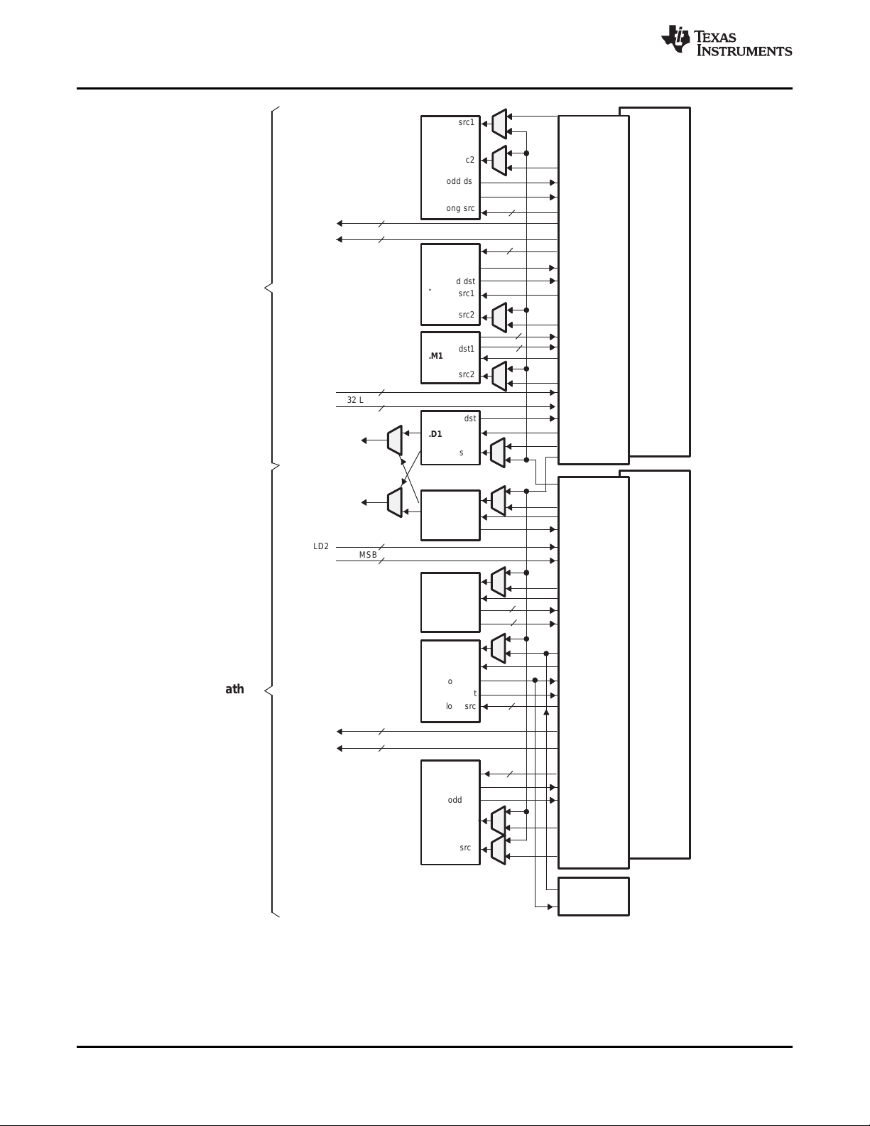
src2
src2
.D1
.M1
.S1
.L1
long src
odd dst
src2
src1
src1
src1
src1
even dst
even dst
odd dst
dst1
dst
src2
src2
src2
long src
DA1
ST1b
LD1b
LD1a
ST1a
Data path A
Odd
register
file A
(A1, A3,
A5...A31)
Odd
register
file B
(B1, B3,
B5...B31)
.D2
src1
dst
src2
DA2
LD2a
LD2b
src2
.M2
src1
dst1
.S2
src1
even dst
long src
odd dst
ST2a
ST2b
long src
.L2
even dst
odd dst
src1
Data path B
Control Register
32 MSB
32 LSB
dst2
(A)
32 MSB
32 LSB
2x
1x
32 LSB
32 MSB
32 LSB
32 MSB
dst2
(B)
(B)
(A)
8
8
8
8
32
32
32
32
(C)
(C)
Even
register
file A
(A0, A2,
A4...A30)
Even
register
file B
(B0, B2,
B4...B30)
(D)
(D)
(D)
(D)
A. On .M unit, dst2 is 32 MSB.
B. On .M unit, dst1 is 32 LSB.
C. On C64x CPU .M unit, src2 is 32 bits; on C64x+ CPU .M unit, src2 is 64 bits.
D. On .L and .S units, odd dst connects to odd register files and even dst connects to even register files.
TMS320C6454
SPRS311F–APRIL 2006–REVISED SEPTEMBER 2010
www.ti.com
Figure 2-1. TMS320C64x+™ CPU (DSP Core) Data Paths
10 Device Overview Copyright © 2006–2010, Texas Instruments Incorporated
Submit Documentation Feedback
Product Folder Link(s): TMS320C6454
Page 11
TMS320C6454
www.ti.com
SPRS311F–APRIL 2006–REVISED SEPTEMBER 2010
2.3 Memory Map Summary
Table 2-2 shows the memory map address ranges of the C6454 device. The external memory
configuration register address ranges in the C6454 device begin at the hex address location 0x7000 0000
for EMIFA and hex address location 0x7800 0000 for DDR2 Memory Controller.
Table 2-2. C6454 Memory Map Summary
MEMORY BLOCK DESCRIPTION BLOCK SIZE (BYTES) HEX ADDRESS RANGE
Reserved 1024K 0000 0000 - 000F FFFF
Internal ROM 32K 0010 0000 - 0010 7FFF
Reserved 7M - 32K 0010 8000 - 007F FFFF
Internal RAM (L2) [L2 SRAM] 1M 0080 0000 - 009F FFFF
Reserved 4M 00A0 0000 - 00DF FFFF
L1P SRAM 32K 00E0 0000 - 00E0 7FFF
Reserved 1M - 32K 00E0 8000 - 00EF FFFF
L1D SRAM 32K 00F0 0000 - 00F0 7FFF
Reserved 1M - 32K 00F0 8000 - 00FF FFFF
Reserved 8M 0100 0000 - 017F FFFF
C64x+ Megamodule Registers 4M 0180 0000 - 01BF FFFF
Reserved 12.5M 01C0 0000 - 0287 FFFF
HPI Control Registers 256K 0288 0000 - 028B FFFF
McBSP 0 Registers 256K 028C 0000 - 028F FFFF
McBSP 1 Registers 256K 0290 0000 - 0293 FFFF
Timer 0 Registers 256K 0294 0000 - 0297 FFFF
Timer 1 Registers 128K 0298 0000 - 0299 FFFF
PLL1 Controller (including Reset Controller) Registers 512 029A 0000 - 029A 01FF
Reserved 256K - 512 029A 0200 - 029B FFFF
PLL2 Controller Registers 512 029C 0000 - 029C 01FF
Reserved 64K 029C 0200 - 029C FFFF
EDMA3 Channel Controller Registers 32K 02A0 0000 - 02A0 7FFF
Reserved 96K 02A0 8000 - 02A1 FFFF
EDMA3 Transfer Controller 0 Registers 32K 02A2 0000 - 02A2 7FFF
EDMA3 Transfer Controller 1 Registers 32K 02A2 8000 - 02A2 FFFF
EDMA3 Transfer Controller 2 Registers 32K 02A3 0000 - 02A3 7FFF
EDMA3 Transfer Controller 3 Registers 32K 02A3 8000 - 02A3 FFFF
Reserved 256K 02A4 0000 - 02A7 FFFF
Chip-Level Registers 256K 02A8 0000 - 02AB FFFF
Device State Control Registers 256K 02AC 0000 - 02AF FFFF
GPIO Registers 16K 02B0 0000 - 02B0 3FFF
I2C Data and Control Registers 256K 02B0 4000 - 02B3 FFFF
Reserved 720K 02B4 0000 - 02BF FFFF
PCI Control Registers 256K 02C0 0000 - 02C3 FFFF
Reserved 256K 02C4 0000 - 02C7 FFFF
EMAC Control 4K 02C8 0000 - 02C8 0FFF
EMAC Control Module Registers 2K 02C8 1000 - 02C8 17FF
MDIO Control Registers 2K 02C8 1800 - 02C8 1FFF
EMAC Descriptor Memory 8K 02C8 2000 - 02C8 3FFF
Reserved 496K 02C8 4000 - 02CF FFFF
Reserved 220M 02D0 0000 - 0FFF FFFF
Reserved 256M 1000 0000 - 1FFF FFFF
Copyright © 2006–2010, Texas Instruments Incorporated Device Overview 11
Submit Documentation Feedback
Product Folder Link(s): TMS320C6454
Page 12
TMS320C6454
SPRS311F–APRIL 2006–REVISED SEPTEMBER 2010
Table 2-2. C6454 Memory Map Summary (continued)
MEMORY BLOCK DESCRIPTION BLOCK SIZE (BYTES) HEX ADDRESS RANGE
Reserved 256M 2000 0000 - 2FFF FFFF
McBSP 0 Data 256 3000 0000 - 3000 00FF
Reserved 64M - 256 3000 0100 - 33FF FFFF
McBSP 1 Data 256 3400 0000 - 3400 00FF
Reserved 64M - 256 3400 0100 - 37FF FFFF
Reserved 64M 3800 0000 - 3BFF FFFF
Reserved 2K 3C00 0000 - 3C00 07FF
Reserved 16M - 2K 3C00 0800 - 3CFF FFFF
Reserved 48M 3D00 0000 - 3FFF FFFF
PCI External Memory Space 256M 4000 0000 - 4FFF FFFF
Reserved 256M 5000 0000 - 5FFF FFFF
Reserved 256M 6000 0000 - 6FFF FFFF
EMIFA (EMIF64) Configuration Registers 128M 7000 0000 - 77FF FFFF
DDR2 Memory Controller Configuration Registers 128M 7800 0000 - 7FFF FFFF
Reserved 256M 8000 0000 - 8FFF FFFF
Reserved 256M 9000 0000 - 9FFF FFFF
EMIFA CE2 - SBSRAM/Async
Reserved 256M - 8M A080 0000 - AFFF FFFF
EMIFA CE3 - SBSRAM/Async
Reserved 256M - 8M B080 0000 - BFFF FFFF
EMIFA CE4 - SBSRAM/Async
Reserved 256M - 8M C080 0000 - CFFF FFFF
EMIFA CE5 - SBSRAM/Async
Reserved 256M - 8M D080 0000 - DFFF FFFF
DDR2 Memory Controller CE0 - DDR2 SDRAM 512M E000 0000 - FFFF FFFF
(1) The EMIFA CE0 and CE1 are not functionally supported on the C6454 device and, therefore, are not pinned out.
(1)
(1)
(1)
(1)
8M A000 0000 - A07F FFFF
8M B000 0000 - B07F FFFF
8M C000 0000 - C07F FFFF
8M D000 0000 - D07F FFFF
www.ti.com
12 Device Overview Copyright © 2006–2010, Texas Instruments Incorporated
Submit Documentation Feedback
Product Folder Link(s): TMS320C6454
Page 13

TMS320C6454
www.ti.com
2.4 Boot Sequence
The boot sequence is a process by which the DSP's internal memory is loaded with program and data
sections and the DSP's internal registers are programmed with predetermined values. The boot sequence
is started automatically after each power-on reset, warm reset, and system reset. For more details on the
initiators of these resets, see Section 7.6, Reset Controller.
There are several methods by which the memory and register initialization can take place. Each of these
methods is referred to as a boot mode. The boot mode to be used is selected at reset through the
BOOTMODE[3:0] pins.
Each boot mode can be classified as a hardware boot mode or as a software boot mode. Software boot
modes require the use of the on-chip bootloader. The bootloader is DSP code that transfers application
code from an external source into internal or external program memory after the DSP is taken out of reset.
The bootloader is permanently stored in the internal ROM of the DSP starting at byte address 0010
0000h. Hardware boot modes are carried out by the boot configuration logic. The boot configuration logic
is actual hardware that does not require the execution of DSP code. Section 2.4.1, Boot Modes
Supported, describes each boot mode in more detail.
When accessing the internal ROM of the DSP, the CPU frequency must always be less than 750 MHz.
Therefore, when using a software boot mode, care must be taken such that the CPU frequency does not
exceed 750 MHz at any point during the boot sequence. After the boot sequence has completed, the CPU
frequency can be programmed to the frequency required by the application.
2.4.1 Boot Modes Supported
SPRS311F–APRIL 2006–REVISED SEPTEMBER 2010
The C6454 device has five boot modes:
• No boot (BOOTMODE[3:0] = 0000b)
With no boot, the CPU executes directly from the internal L2 SRAM located at address 0x80 0000.
Note: device operations is undefined if invalid code is located at address 0x80 0000. This boot mode is
a hardware boot mode.
• Host boot (BOOTMODE[3:0] = 0001b and BOOTMODE[3:0] = 0111b)
If host boot is selected, after reset, the CPU is internally "stalled" while the remainder of the device is
released. During this period, an external host can initialize the CPU's memory space as necessary
through Host Port Interface (HPI) or the Peripheral Component Interconnect (PCI) interface. Internal
configuration registers, such as those that control the EMIF can also be initialized by the host with two
exceptions: Device State Control registers (Section 3.4), PLL1 and PLL2 Controller registers
(Section 7.7 and Section 7.8) cannot be accessed through any host interface, including HPI and PCI.
Once the host is finished with all necessary initialization, it must generate a DSP interrupt (DSPINT) to
complete the boot process. This transition causes boot configuration logic to bring the CPU out of the
"stalled" state. The CPU then begins execution from the internal L2 SRAM located at 0x80 0000. Note
that the DSP interrupt is registered in bit 0 (channel 0) of the EDMA Event Register (ER). This event
must be cleared by software before triggering transfers on DMA channel 0.
All memory, with the exceptions previously described, may be written to and read by the host. This
allows for the host to verify what it sends to the DSP if required. After the CPU is out of the "stalled"
state, the CPU needs to clear the DSPINT, otherwise, no more DSPINTs can be received.
As previously mentioned, for the C6454 device, the Host Port Interface (HPI) and the Peripheral
Component Interconnect (PCI) interface can be used for host boot. To use the HPI for host boot, the
PCI_EN pin (Y29) must be low [default] (enabling the HPI peripheral) and BOOTMODE[3:0] must be
set to 0001b at device reset. Conversely, to use the PCI interface for host boot, the PCI_EN pin (Y29)
must be high (enabling the PCI peripheral) and BOOTMODE[3:0] must be set to 0111b at device reset.
For the HPI host boot, the DSP interrupt can be generated through the use of the DSPINT bit in the
HPI Control (HPIC) register.
For the HPI host boot, the CPU is actually held in reset until a DSP interrupt is generated by the host.
The DSP interrupt can be generated through the use of the DSPINT bit in the HPI Control (HPIC)
register. Since the CPU is held in reset during HPI host boot, it will not respond to emulation software
Copyright © 2006–2010, Texas Instruments Incorporated Device Overview 13
Submit Documentation Feedback
Product Folder Link(s): TMS320C6454
Page 14

TMS320C6454
SPRS311F–APRIL 2006–REVISED SEPTEMBER 2010
such as Code Composer Studio.
For the PCI host boot, the CPU is out of reset, but it executes an IDLE instruction until a DSP interrupt
is generated by the host. The host can generate a DSP interrupt through the PCI peripheral by setting
the DSPINT bit in the Back-End Application Interrupt Enable Set Register (PCIBINTSET) and the
Status Set Register (PCISTATSET).
Note that the HPI host boot is a hardware boot mode while the PCI host boot is a software boot mode.
If PCI boot is selected, the on-chip bootloader configures the PLL1 Controller such that CLKIN1 is
multiplied by 15. More specifically, PLLM is set to 0Eh (x15) and RATIO is set to 0 (÷1) in the PLL1
Multiplier Control Register (PLLM) and PLL1 Pre-Divider Register (PREDIV), respectively. The CLKIN1
frequency must not be greater than 50 MHz so that the maximum speed of the internal ROM, 750
MHz, is not violated. The CFGGP[2:0] pins must be set to 000b during reset for proper operation of the
PCI boot mode.
As mentioned previously, a DSP interrupt must be generated at the end of the host boot process to
begin execution of the loaded application. Since the DSP interrupt generated by the HPI and PCI is
mapped to the EDMA event DSP_EVT (DMA channel 0), it will get recorded in bit 0 of the EDMA
Event Register (ER). This event must be cleared by software before triggering transfers on DMA
channel 0.
• EMIFA 8-bit ROM boot (BOOTMODE[3:0] = 0100b)
After reset, the device will begin executing software out of an Asynchronous 8-bit ROM located in
EMIFA CE3 space using the default settings in the EMIFA registers. This boot mode is a hardware
boot mode.
• Master I2C boot (BOOTMODE[3:0] = 0101b)
After reset, the DSP can act as a master to the I2C bus and copy data from an I2C EEPROM or a
device acting as an I2C slave to the DSP using a predefined boot table format. The destination
address and length are contained within the boot table. This boot mode is a software boot mode.
• Slave I2C boot (BOOTMODE[3:0] = 0110b)
A Slave I2C boot is also implemented, which programs the DSP as an I2C Slave and simply waits for a
Master to send data using a standard boot table format.
Using the Slave I2C boot, a single DSP or a device acting as an I2C Master can simultaneously boot
multiple slave DSPs connected to the same I2C bus. Note that the Master DSP may require booting
via an I2C EEPROM before acting as a Master and booting other DSPs.
The Slave I2C boot is a software boot mode.
www.ti.com
2.4.2 2nd-Level Bootloaders
Any of the boot modes can be used to download a 2nd-level bootloader. A 2nd-level bootloader allows for
any level of customization to current boot methods as well as definition of a completely customized boot.
TI offers a few 2nd-level bootloaders, such as an EMAC bootloader, which can be loaded using the
Master I2C boot.
14 Device Overview Copyright © 2006–2010, Texas Instruments Incorporated
Submit Documentation Feedback
Product Folder Link(s): TMS320C6454
Page 15
AG
AF
AE
AD
AC
AB
AA
Y
W
V
U
T
R
13121110987654321
13121110987654321
CLKR1/
GP[0]
HD15/
AD15
HD2/
AD2
PGNT
/
GP[12]
HD22/
AD22
DV
DD33
RSV15
PIDSEL
RSV16
HDS1
/
PSERR
HINT/
PFRAME
DV
DD33
HHWIL/
PCLK
V
SS
HD12/
AD12
HD24/
AD24
RSV03
HD20/
AD20
HD18/
AD18
HD6/
AD6
HD16/
AD16
V
SS
HD28/
AD28
HD17/
AD17
HD31/
AD31
HD14/
AD14
HCNTL1/
PDEVSEL
HR/W/
PCBE2
HRDY/
PIRDY
PRST/
GP[13]
HD21/
AD21
DV
DD33
V
SS
EMU8
RSV36
EMU11
EMU1
EMU10
EMU12
RSV37
EMU15
EMU4
EMU13
DV
DD33
DV
DD33
V
SS
EMU0
V
SS
DV
DD33
RSV38EMU6
CLKX1/
GP[3]
DV
DD33
V
SS
EMU18
DV
DD33
EMU5
V
SS
DV
DD33
HD9/
AD9
HD23/
AD23
HD3/
AD3
HD10/
AD10
GP[6]
V
SS
EMU14
GP[7]
RSV02
HD4/
AD4
HD30/
AD30
CV
DD
HD27/
AD27
V
SS
V
SS
V
SS
DV
DD33
V
SS
CV
DD
CV
DD
V
SS
DV
DD33
DV
DD33
V
SS
V
SS
DV
DD33
V
SS
V
SS
HD19/
AD19
HD13/
AD13
HD29/
AD29
DV
DD33
DV
DD33
HD25/
AD25
DV
DD33
HD0/
AD0
V
SS
HD11/
AD11
TOUTL0
EMU3
EMU7
TOUTL1
V
SS
DV
DD33
V
SS
DV
DD33
V
SS
HDS2
/
PCBE1
HCNTL0/
PSTOP
HCS/
PPERR
V
SS
HD8/
AD8
V
SS
HD26/
AD26
V
SS
HD7/
AD7
HD1/
AD1
EMU2
RSV39
V
SS
DV
DD33
HAS/
PPAR
HD5/
AD5
AH
TINPL0 EMU17TDONMI EMU16GP[4]V
SS
TRST
TDI
RSV27 EMU9
AJ
TINPL1 TMSV
SS
CLKS RSV40
GP[5]DV
DD33
DV
DD33
TCK
RSV26
SYSCLK4/
GP[1]
14
V
SS
DV
DD33
RESETSTAT
POR
V
SS
CV
DD
CV
DD
RESET
DV
DD33
V
SS
15
RSV64
V
SS
DV
DD33
RSV45
CV
DD
V
SS
V
SS
RSV46
V
SS
DV
DD33
14 15
V
SS
CV
DD
CV
DD
CV
DD
V
SS
V
SS
V
SS
CV
DD
RSV68
V
SS
V
SS
CV
DD
AG
AF
AE
AD
AC
AB
AA
Y
W
V
U
T
R
AH
AJFSX0 DR0
FSR0
DR1/
GP[8]
CLKR0
FSX1/
GP[11]
DX1/
GP[9]
CLKX0
DX0
FSR1/
GP[10]
TMS320C6454
www.ti.com
SPRS311F–APRIL 2006–REVISED SEPTEMBER 2010
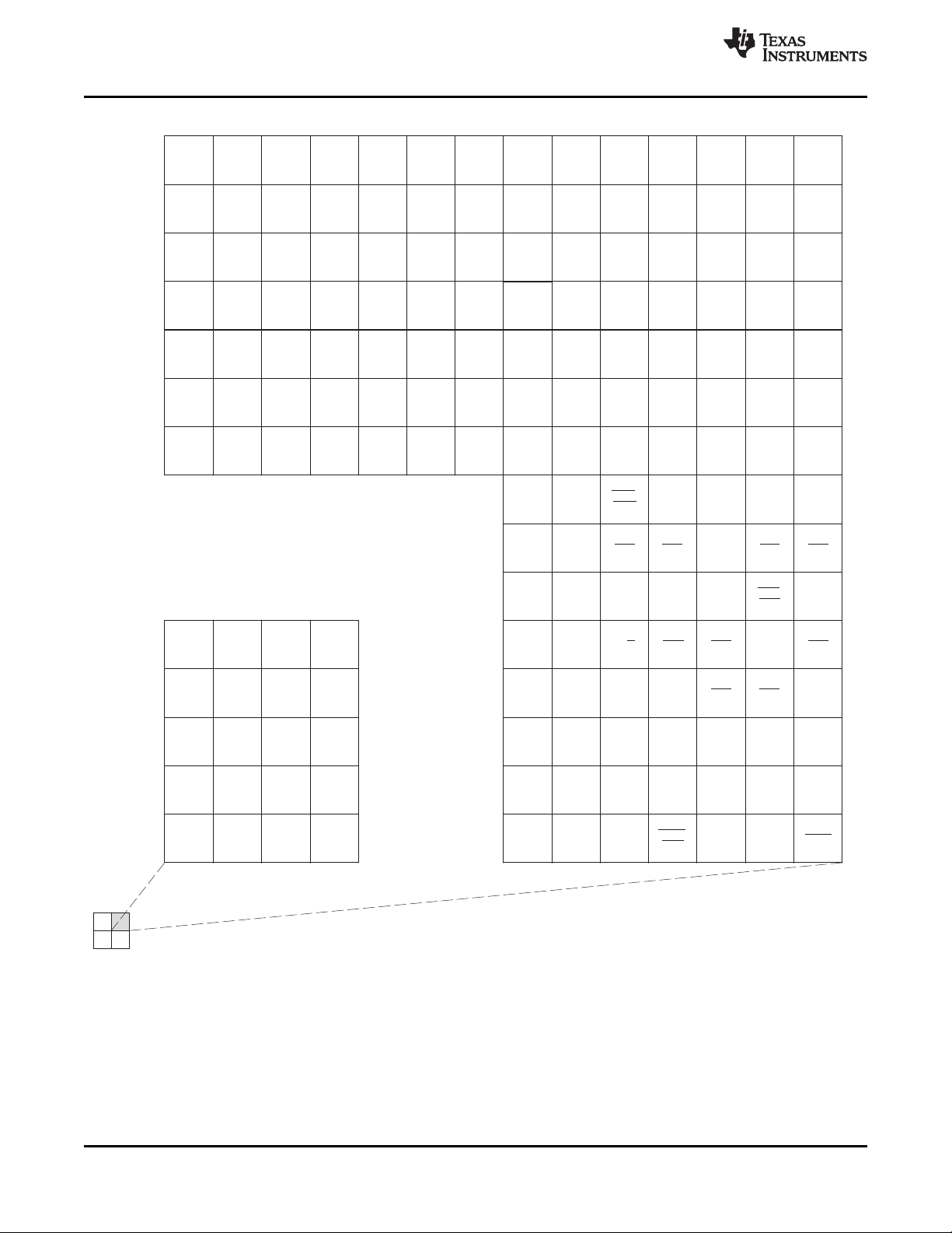
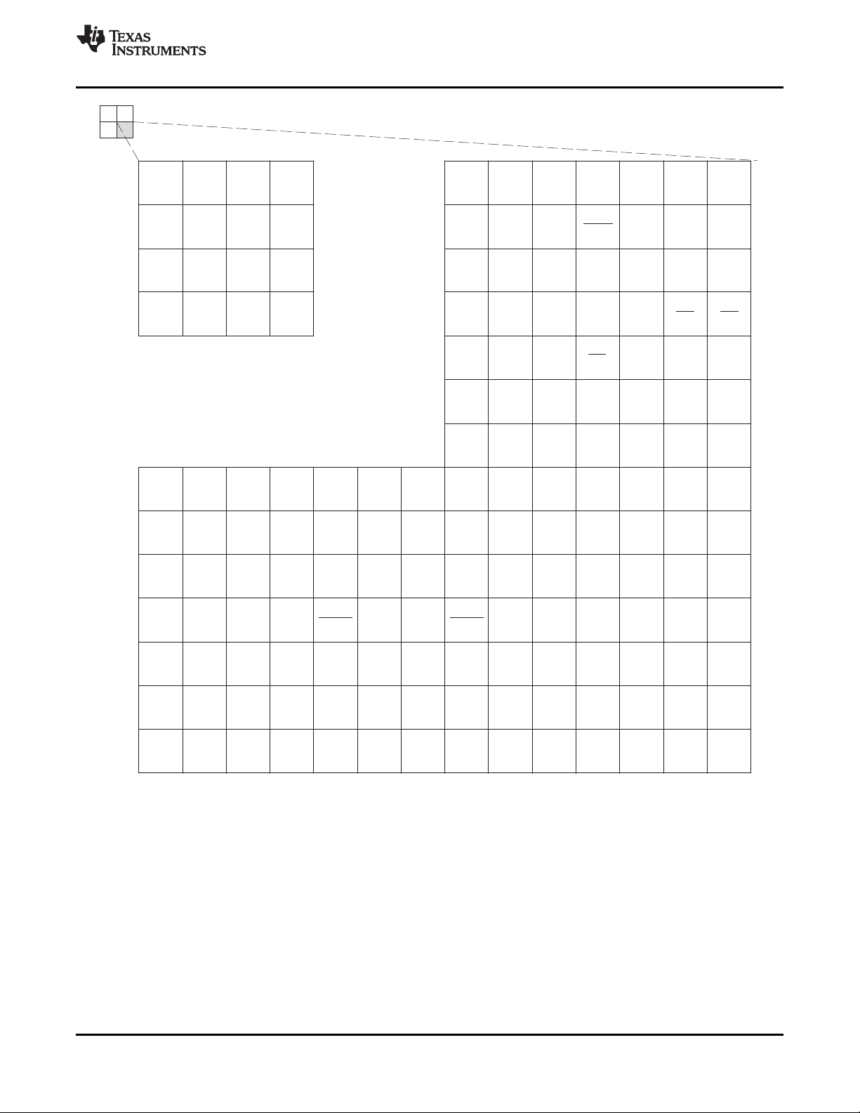
2.5 Pin Assignments
2.5.1 Pin Map
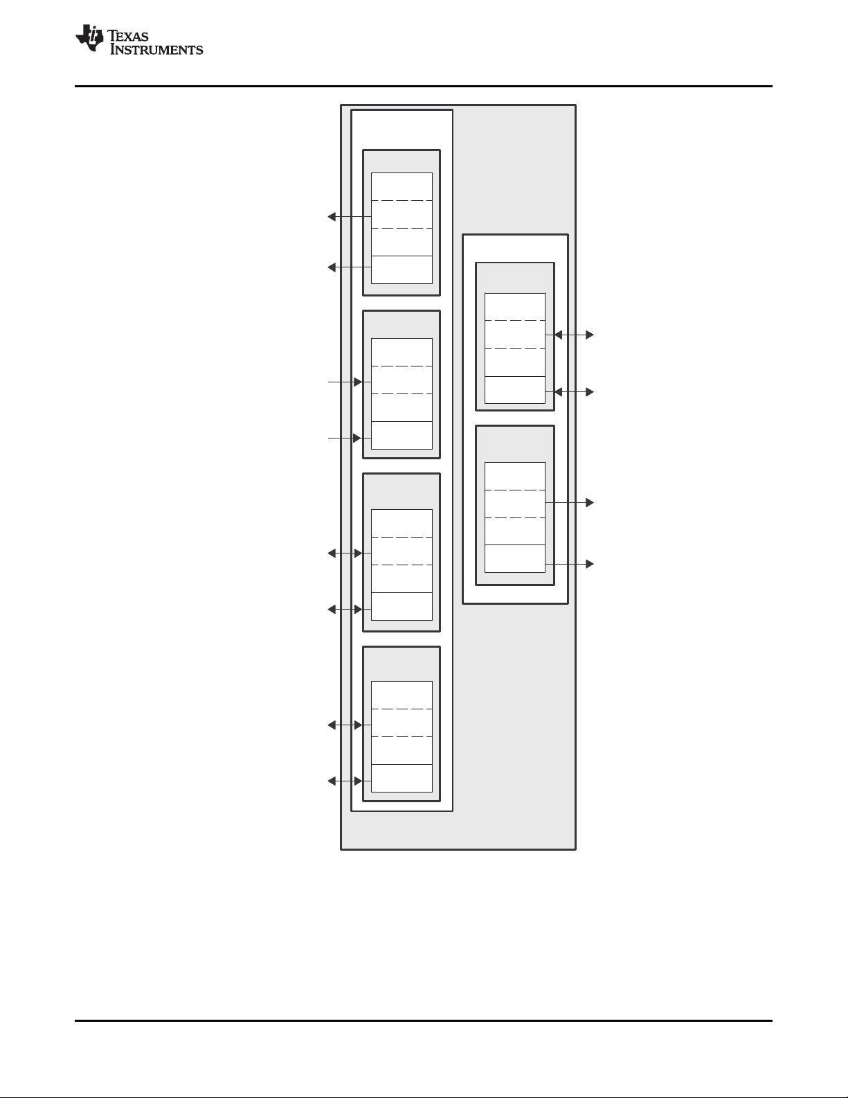
Figure 2-2 through Figure 2-5 show the C6454 device pin assigments in four quadrants (A, B, C, and D).
Copyright © 2006–2010, Texas Instruments Incorporated Device Overview 15
Figure 2-2. C6454 Pin Map (Bottom View) [Quadrant A]
Submit Documentation Feedback
Product Folder Link(s): TMS320C6454
Page 16
AG
AF
AE
AD
AC
AB
AA
Y
W
V
U
T
R
17 18 19 20 21 22 23 24 25 26 27 28 29
17 18 19 20 21 22 23 24 25 26 27 28 29
SDA
AED27
V
SS
ASADS
/
ASRE
AED17
AHOLD
PLLV1
AEA13/
LENDIAN
AEA4/
SYSCLKOUT
_EN
AEA5/
MCBSP1
_EN
AEA6/
PCI66
AECLKOUTACE5
ACE4
ABA0/
DDR2_EN
ABE7
ACE2 RSV41
AAOE
/
ASOE
RSV42 RSV44
ABE2
ABE0
AED29
AED31
ACE3
AEA1/
CFGGP1
AEA11
AEA2/
CFGGP2
AEA14/
HPI_
WIDTH
AED21
DV
DD33
V
SS
V
SS
V
SS
DV
DD33
RSV73
RSV63
V
SS
V
SS
RSV17
V
SS
DV
DD33
V
SS
V
SS
RSV74
RSV50
DV
DD33
V
SS
DV
DD33
V
SS
AED3V
SS
RSV49
AED7
AED1
SCL
RSV65
V
SS
RSV72
RSV48
V
SS
DV
DD33
V
SS
AED25
AED28
AED11
AED4
AED9
AED15RSV47
AED16
ABA1/
EMIFA_EN
RSV43
ABE1
RSV71
AED24DV
DD33
V
SS
V
SS
AED19
DV
DD33
CV
DD
CV
DD
DV
DD33
V
SS
V
SS
DV
DD33
DV
DD33
V
SS
V
SS
V
SS
DV
DD33
V
SS
AED26V
SS
DV
DD33
AED22AED0
AED13AED12
AED10RSV54RSV75RSV51
AED30DV
DD33
AEA12
V
SS
V
SS
V
SS
V
SS
RSV20
AEA0/
CFGGP0
V
SS
DV
DD33
AR/W
DV
DD33
PCI_ENDV
DD33
AED23
AAWE
/
ASWE
RSV53RSV52DV
DD33
ABE3
AEA3
AED8
AH
DV
DD33
V
SS
RSV76 RSV58 AED14RSV55 AED2 AED18
V
SS
RSV62VSSV
SS
V
SS
RSV59
AJ
V
SS
DV
DD33
V
SS
RSV57 AED5RSV56 AED6 AED20 DV
DD33
RSV78RSV61RSV60RSV77
16
V
SS
RSV66
V
SS
DV
DD33
V
SS
RSV70
CV
DD
V
SS
DV
DD33
V
SS
16
V
SS
CV
DD
CV
DD
RSV69
V
SS
V
SS
V
SS
RSV67
V
SS
CV
DD
AG
AF
AE
AD
AC
AB
AA
Y
W
V
U
T
R
AH
AJ
TMS320C6454
SPRS311F–APRIL 2006–REVISED SEPTEMBER 2010
www.ti.com
Figure 2-3. C6454 Pin Map (Bottom View) [Quadrant B]
16 Device Overview Copyright © 2006–2010, Texas Instruments Incorporated
Submit Documentation Feedback
Product Folder Link(s): TMS320C6454
Page 17
C
D
E
F
G
H
J
K
L
M
N
P
17 18 19 20 21 22 23 24 25 26 27 28 29
17 18 19 20 21 22 23 24 25 26 27 28 29
RSV09
AED52
DV
DD33
V
SS
V
SS
V
SS
AECLKIN
AEA9/
MACSEL0
CLKIN1
DV
DD33
AEA15/
AECLKIN
_SEL
AED40AED44 AED42
AED34
ABE6
AED32
ABE4
AEA18/
BOOT
MODE2
AED37
ABUSREQ
AED46
AEA16/
BOOT
MODE0
AEA19/
BOOT
MODE3
AHOLDA
AEA10/
MACSEL1
V
SS
V
SS
DV
DD18
DED19
V
SS
CV
DD
VSSDSDDQS2
DSDDQ
GATE2
DED23
DV
DD18
DV
DD33
DSDDQS3
DSDDQS3
V
SS
DV
DD18
RSV11
RSV12 RSV33DSDDQM2 DED26
V
SS
RSV32
RSV23
V
SS
V
SS
DEA4
DEA1
AV
DLL2
DV
DD33
DV
DD33
AED56
AED50
AED45
AED59
AED61
AED58DEA5
AED60
AED33
AEA17/
BOOT
MODE1
DSDDQ
GATE3
RSV19
AED55V
SS
DV
DD18
DV
DD18
AED39
DV
DD33
V
SS
V
SS
RSV30
DV
DD33
V
SS
V
SS
DV
DD18
V
SS
DV
DD18
DV
DD18
AED35AED48AED54DV
DD18
V
SS
DV
DD33
AED47
DV
DD33
DV
DD33
AED57DED27DSDDQS2
DEA0
AED41DSDDQM3
DV
DD33
V
SS
CV
DD
V
SS
CV
DD
V
SS
AEA8/
PCI_EEAI
RSV31
AED38
V
SS
AARDY
V
SS
AED36AED63
V
SS
DED22DED18DEA6
ABE5
AEA7
AED43
B
DED29 DED31DV
DD18
DED25
RSV22
DEA2 AED49 AED51
V
SS
DV
DD18
DED21DED16DEA7
A
DED28 DED30V
SS
DED24 DV
DD18MON
DEA3 AED62 AED53 DV
DD33
V
SS
DED20DED17DEODT1
16
DV
DD18
CV
DD
DEODT0
DEA8
CV
DD
V
SS
V
SS
DEA9
DEA10
DEA11
16
CV
DD
V
SS
V
SS
CV
DD
V
SS
CV
DD
C
D
E
F
G
H
J
K
L
M
N
P
B
A
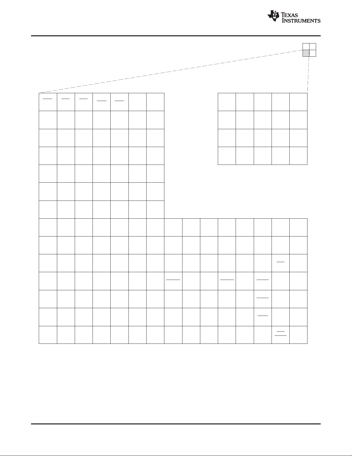
TMS320C6454
www.ti.com
SPRS311F–APRIL 2006–REVISED SEPTEMBER 2010
Figure 2-4. C6454 Pin Map (Bottom View) [Quadrant C]
Copyright © 2006–2010, Texas Instruments Incorporated Device Overview 17
Submit Documentation Feedback
Product Folder Link(s): TMS320C6454
Page 18
A
D
E
F
G
H
J
K
L
M
N
P
13121110987654321
13121110987654321
RGRXD2
RGTXD3
DV
DD33
MTXD2
V
SS
MTXD0/
RMTXD0
CV
DDMON
MTXD6
V
SS
PREQ
/
GP[15]
PINTA/
GP[14]
MRXD2 MRXD3
MRXD0/
RMRXD0
V
SS
MTXD3MCOL
MRXD5
MTXD1/
RMTXD1
DV
DD15
MTXD4
MCRS/
RMCRSDV
PTRDY
MTXD7
MTCLK/
RMREFCLK
MDCLK
RGRXD3
DV
DD18
DED1
DSDDQS0
DSDDQM0 DED2
DSDDQS0
DED6
DED7
DED8
DED9
DED10
DSDDQM1
DSDDQS1
DED15
DED14
V
SS
RSV25
RSV35
RSV34
V
SS
DV
DD15
V
SS
V
SS
DV
DD15
V
SS
V
SS
DSDWE
DSDRAS
DSDCAS
V
SS
DED3
RSV29
DV
DD33
RGTXD0
RGTXD1
RGREFCLK
RGTXCTL
DV
DD15MON
RGRXD1 RSV18
RSV13
GMTCLK
MTXD5
DSDDQ
GATE0
DED0
DV
DD15
DED12 DV
DD18
DED5
RGRXD0
DV
DD33
V
SS
V
SS
V
SS
DV
DD33MONVSS
RSV21 DED13 DED4 V
SS
AV
DLL1
V
SSVREFHSTL
RGMDCLK RSV24
DSDDQ
GATE1
RGRXCTL V
SS
DV
DD15
RGTXC
RGRXC DSDDQS1 DV
DD18
DV
DD18
RSV14
DV
DD18
MRXD7 V
SS
CV
DD
RSV28 CV
DD
PCBE0
/
GP[2]
PCBE3 DV
DD33
MTXEN/
RMTXEN
V
SS
DV
DD33
V
SS
RGMDIO PLLV2 V
SS
DED11
DV
DD18
DV
DD18
MRXD4
MDIO
RGTXD2
B
DV
DD15
V
SS
DV
DD18
DV
DD18
RSV07 DV
DD18
CLKIN2DV
DD33
V
SS
V
SS
V
SS
V
SS
V
SS
C
V
SS
MRXDV
MRXER/
RMRXER
CV
DD
MRXD1/
RMRXD1
MRXD6MRCLK DV
DD15
V
SS
V
SS
14
DDR2
CLKOUT
V
REFSSTL
DSDCKE
DCE0
CV
DD
DDR2
CLKOUT
V
SS
V
SS
DV
DD18
CV
DD
15
DEA13
DBA0
DBA1
DBA2
V
SS
DEA12
CV
DD
DV
DD18
V
SS
V
SS
14 15
CV
DD
RSV04
V
SS
CV
DD
V
SS
CV
DD
RSV05
F
D
E
A
G
H
J
K
L
M
N
P
B
C
TMS320C6454
SPRS311F–APRIL 2006–REVISED SEPTEMBER 2010
www.ti.com
Figure 2-5. C6454 Pin Map (Bottom View) [Quadrant D]
18 Device Overview Copyright © 2006–2010, Texas Instruments Incorporated
Submit Documentation Feedback
Product Folder Link(s): TMS320C6454
Page 19
TRST
IEEE Standard
1149.1
(JTAG)
Emulation
Reserved
Reset and
Interrupts
Control/Status
TDI
TDO
TMS
TCK
NMI
RESET
RSV03
RSV04
Clock/PLL1
and
PLL Controller
CLKIN1
EMU0
EMU1
SYSCLK4/GP[1]
(A)
EMU14
EMU15
EMU16
EMU17
RSV02
EMU18
RSV06
RSV07
RSV05
RSV77
RSV78
RSV76
•
•
•
•
•
•
RESETSTAT
CLKIN2
POR
PCI_EN
Peripheral
Enable/Disable
Clock/PLL2
PLLV2
PLLV1
A. This pin functions as GP[1] by default. For more details, see the Device Configuration section of this document.
TMS320C6454
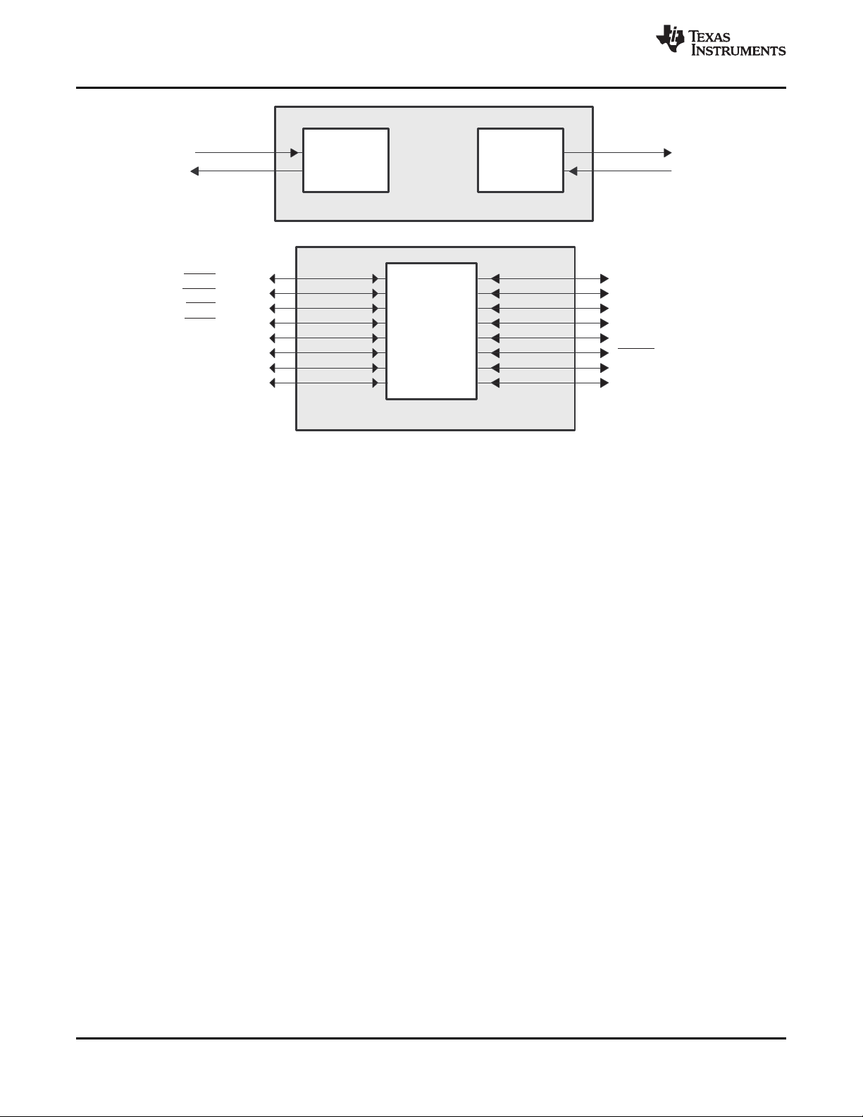
www.ti.com
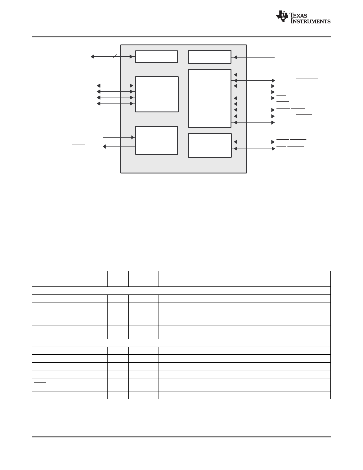
2.6 Signal Groups Description
SPRS311F–APRIL 2006–REVISED SEPTEMBER 2010
A. This pin functions as GP[1] by default. For more details, see Section 3.
Figure 2-6. CPU and Peripheral Signals
Copyright © 2006–2010, Texas Instruments Incorporated Device Overview 19
Submit Documentation Feedback
Product Folder Link(s): TMS320C6454
Page 20
A. This pin functions as GP[1] by default. For more details, see the Device Configuration section of this document.
B. These McBSP1 peripheral pins are muxed with the GPIO peripheral pins and by default these signals function as GPIO peripheral pins. For
more details, see the Device Configuration section of this document.
C. These PCI peripheral pins are muxed with the GPIO peripheral pins and by default these signals function as GPIO peripheral pins. For more
details, see the Device Configuration section of this document.
GPIO
General-Purpose Input/Output 0 (GPIO) Port
CLKX1/GP[3]
(B)
PCBE0
/GP[2]
(C)
SYSCLK4/GP[1]
(A)
PREQ
/GP[15]
(C)
PINTA
/GP[14]
(C)
PRST
/GP[13]
(C)
PGNT
/GP[12]
(C)
FSX1/GP[11]
(B)
FSR1/GP[10]
(B)
DX1/GP[9]
(B)
DR1/GP[8]
(B)
GP[7]
GP[6]
GP[5]
GP[4]
CLKR1/GP[0]
(B)
Timers (64-Bit)
TINPL1
Timer 1
Timer 0
TOUTL1
TINPL0
TOUTL0
TMS320C6454
SPRS311F–APRIL 2006–REVISED SEPTEMBER 2010
www.ti.com
Figure 2-7. Timers/GPIO Peripheral Signals
20 Device Overview Copyright © 2006–2010, Texas Instruments Incorporated
Submit Documentation Feedback
Product Folder Link(s): TMS320C6454
Page 21

ACE4
(A)
AECLKOUT
AED[63:0]
ACE3
(A)
ACE2
(A)
AEA[19:0]
AARDY
Data
Memory Map
Space Select
Address
Byte Enables
64
20
External
Memory I/F
Control
EMIFA (64-bit Data Bus)
AECLKIN
AHOLD
AHOLDA
ABUSREQ
Bus
Arbitration
ABE3
ABE2
ABE1
ABE0
ASWE/AAWE
DDR2CLKOUT
DED[31:0]
DCE0
DEA[13:0]
Data
Memory Map
Space Select
Address
Byte Enables
32
14
External
Memory I/F
Control
DDR2 Memoty Controller (32-bit Data Bus)
DSDCAS
DSDCKE
DDR2CLKOUT
DSDDQS[3:0]
DSDRAS
DSDWE
DSDDQS[3:0]
ABE7
ABE6
ABE5
ABE4
ACE5
(A)
Bank Address
ABA[1:0]
AR/W
AAOE/ASOE
ASADS/ASRE
Bank Address
DBA[2:0]
DEODT[1:0]
DSDDQGATE[0]
DSDDQM3
DSDDQM2
DSDDQM1
DSDDQM0
DSDDQGATE[1]
DSDDQGATE[2]
DSDDQGATE[3]
TMS320C6454
www.ti.com
SPRS311F–APRIL 2006–REVISED SEPTEMBER 2010
Figure 2-8. EMIFA and DDR2 Memory Controller Peripheral Signals
Copyright © 2006–2010, Texas Instruments Incorporated Device Overview 21
Submit Documentation Feedback
Product Folder Link(s): TMS320C6454
Page 22
McBSPs
(Multichannel Buffered Serial Ports)
(B)
CLKX0
FSX0
DX0
CLKR0
FSR0
DR0
Transmit
McBSP0
Receive
Clock
CLKX1/GP[3]
FSX1/GP[11]
DX1/GP[9]
CLKR1/GP[0]
FSR1/GP[10]
DR1/GP[8]
Transmit
McBSP1
Receive
Clock
HHWIL/PCLK
HCNTL0/PSTOP
HCNTL1/PDEVSEL
Data
Register Select
Half-Word
Select
Control
HPI
(A)
(Host-Port Interface)
32
HAS/PPAR
HR/W
/PCBE2
HCS/PPERR
HDS1/PSERR
HDS2/PCBE1
HRDY/PIRDY
HINT/PFRAME
(HPI16 ONL Y)
HD[15:0]/AD[15:0]
HD[31:16]/AD[31:16]
SCL
I2C
SDA
A. These HPI pins are muxed with the PCI peripheral. By default, these pins function as HPI. When the HPI is enabled, the number of HPI pins
used depends on the HPI configuration (HPI16 or HPI32). For more details on these muxed pins, see the Device Configuration section of this
document.
B. These McBSP1 peripheral pins are muxed with the GPIO peripheral pins and by default these signals function as GPIO peripheral pins. For
more details, see the Device Configuration section of this document.
CLKS
(SHARED)
TMS320C6454
SPRS311F–APRIL 2006–REVISED SEPTEMBER 2010
www.ti.com
Figure 2-9. HPI/McBSP/I2C Peripheral Signals
22 Device Overview Copyright © 2006–2010, Texas Instruments Incorporated
Submit Documentation Feedback
Product Folder Link(s): TMS320C6454
Page 23
RGTXCTL, RGRXCTL
MRXER/RMRXER,
MRXDV,
MCRS/RMCRSDV,
MCOL,
MTXEN/RMTXEN
Ethernet MAC (EMAC) and MDIO
MDIO
MDCLK
MDIO
Clock
Clocks
Error Detect
and Control
Input/Output
Receive
RGMDIO
RGMDCLK
RGTXD[3:0]
A. RGMII signals are mutually exclusive to all other EMAC signals.
RGTXC,
RGRXC,
RGREFCLK
MTXD[7:2],
MTXD[1:0]/RMTXD[1:0]
Transmit
RGMII
(A)
GMII
RMII
MII
RGRXD[3:0]
MRXD[7:2],
MRXD[1:0]/RMRXD[1:0]
RGMII
(A)
GMII
RMII
MII
RGMII
(A)
GMII
RMII
MII
RGMII
(A)
GMII
RMII
MII
RGMII
(A)
GMII
RMII
MII
GMII
RMII
MII
RGMII
(A)
MTCLK/RMREFCLK,
MRCLK,
GMTCLK
Ethernet MAC
(EMAC)
TMS320C6454
www.ti.com
SPRS311F–APRIL 2006–REVISED SEPTEMBER 2010
Copyright © 2006–2010, Texas Instruments Incorporated Device Overview 23
Figure 2-10. EMAC/MDIO [MII, GMII, RMII, and RGMII] Peripheral Signals
Submit Documentation Feedback
Product Folder Link(s): TMS320C6454
Page 24
HD[15:0]/AD[15:0]
HR/W
/PCBE2
HDS2/PCBE1
PCBE0/GP[2]
HHWIL/PCLK
HINT/PFRAME
PINTA/GP[14]
Data/Address
Arbitration
32
Clock
Control
PCI Interface
(A)
HAS/PPAR
PRST
/GP[13]
HRDY
/PIRDY
HCNTL0/PSTOP
PTRDY
PCBE3
PIDSEL
HCNTL1/PDEVSEL
HDS1/PSERR
Error
Command
Byte Enable
HCS/PPERR
PGNT/GP[12]
PREQ
/GP[15]
HD[31:16]/AD[31:16]
A. These PCI pins are muxed with the HPI or GPIO peripherals. By default, these signals function as HPI or GPIO or EMAC. For more
details on these muxed pins, see the Device Configuration section of this document.
TMS320C6454
SPRS311F–APRIL 2006–REVISED SEPTEMBER 2010
Figure 2-11. PCI Peripheral Signals
www.ti.com
2.7 Terminal Functions
The terminal functions table (Table 2-3) identifies the external signal names, the associated pin (ball)
numbers along with the mechanical package designator, the pin type (I, O/Z, or I/O/Z), whether the pin
has any internal pullup/pulldown resistors, and a functional pin description. For more detailed information
on device configuration, peripheral selection, multiplexed/shared pins, and pullup/pulldown resistors, see
Section 3, Device Configuration.
Table 2-3. Terminal Functions
SIGNAL
NAME NO.
CLKIN1 N28 I IPD Clock Input for PLL1.
CLKIN2 G3 I IPD Clock Input for PLL2.
PLLV1 T29 A 1.8-V I/O supply voltage for PLL1
PLLV2 A5 A 1.8-V I/O supply voltage for PLL2
SYSCLK4/GP[1]
TMS AJ10 I IPU JTAG test-port mode select
TDO AH8 O/Z IPU JTAG test-port data out
TDI AH9 I IPU JTAG test-port data in
TCK AJ9 I IPU JTAG test-port clock
TRST AH7 I IPD
(4)
EMU0
(1) I = Input, O = Output, Z = High impedance, S = Supply voltage, GND = Ground, A = Analog signal
(2) IPD = Internal pulldown, IPU = Internal pullup. For most systems, a 1-kΩ resistor can be used to oppose the IPU/IPD. For more detailed
information on pullup/pulldown resistors and situations where external pullup/pulldown resistors are required, see Section 3.7,
Pullup/Pulldown Resistors.
(3) These pins are multiplexed pins. For more details, see Section 3, Device Configuration.
(4) The C6454 DSP does not require external pulldown resistors on the EMU0 and EMU1 pins for normal or boundary-scan operation.
24 Device Overview Copyright © 2006–2010, Texas Instruments Incorporated
(3)
AJ13 I/O/Z IPD
AF7 I/O/Z IPU Emulation pin 0
TYPE
(1)
IPD/IPU
(2)
CLOCK/PLL CONFIGURATIONS
SYSCLK4 is the clock output at 1/8 of the device speed (O/Z) or this pin can be
programmed as the GP1 pin (I/O/Z) [default].
JTAG EMULATION
JTAG test-port reset. For IEEE 1149.1 JTAG compatibility, see
Section 7.18.3.1.1.
Submit Documentation Feedback
Product Folder Link(s): TMS320C6454
DESCRIPTION
Page 25
TMS320C6454
www.ti.com
SPRS311F–APRIL 2006–REVISED SEPTEMBER 2010
Table 2-3. Terminal Functions (continued)
SIGNAL
NAME NO.
(4)
EMU1
AE11 I/O/Z IPU Emulation pin 1
EMU2 AG9 I/O/Z IPU Emulation pin 2
EMU3 AF10 I/O/Z IPU Emulation pin 3
EMU4 AF9 I/O/Z IPU Emulation pin 4
EMU5 AE12 I/O/Z IPU Emulation pin 5
EMU6 AG8 I/O/Z IPU Emulation pin 6
EMU7 AF12 I/O/Z IPU Emulation pin 7
EMU8 AF11 I/O/Z IPU Emulation pin 8
EMU9 AH13 I/O/Z IPU Emulation pin 9
EMU10 AD10 I/O/Z IPU Emulation pin 10
EMU11 AD12 I/O/Z IPU Emulation pin 11
EMU12 AE10 I/O/Z IPU Emulation pin 12
EMU13 AD8 I/O/Z IPU Emulation pin 13
EMU14 AF13 I/O/Z IPU Emulation pin 14
EMU15 AE9 I/O/Z IPU Emulation pin 15
EMU16 AH12 I/O/Z IPU Emulation pin 16
EMU17 AH10 I/O/Z IPU Emulation pin 17
EMU18 AE13 I/O/Z IPU Emulation pin 18
RESET AG14 I Device reset
NMI AH4 I IPD
RESETSTAT AE14 O Reset Status pin. The RESETSTAT pin indicates when the device is in reset
POR AF14 I Power on reset.
GP[7] AG2 I/O/Z IPD
GP[6] AG3 I/O/Z IPD
GP[5] AJ2 I/O/Z IPD
GP[4] AH2 I/O/Z IPD
PREQ/ GP[15] P2 I/O/Z
(5)
PINTA
/ GP[14] P3 I/O/Z
PRST/ GP[13] R5 I/O/Z
PGNT/ GP[12] R4 I/O/Z
FSX1/GP[11] AG4 I/O/Z IPD
FSR1/GP[10] AE5 I/O/Z IPD
DX1/GP[9] AG5 I/O/Z IPD
DR1/GP[8] AH5 I/O/Z IPD
CLKX1/GP[3] AF5 I/O/Z IPD
PCBE0/ GP[2] P1 I/O/Z
SYSCLK4/GP[1] AJ13 O/Z IPD
CLKR1/GP[0] AF4 I/O/Z IPD
HOST-PORT INTERFACE (HPI) or PERIPHERAL COMPONENT INTERCONNECT (PCI)
PCI_EN Y29 I IPD
TYPE
(1)
IPD/IPU
(2)
DESCRIPTION
RESETS, INTERRUPTS, AND GENERAL-PURPOSE INPUT/OUTPUTS
Nonmaskable interrupt, edge-driven (rising edge)
Any noise on the NMI pin may trigger an NMI interrupt; therefore, if the NMI pin
is not used, it is recommended that the NMI pin be grounded versus relying on
the IPD.
General-purpose input/output (GPIO) pins (I/O/Z).
PCI peripheral pins or General-purpose input/output (GPIO) [15:12, 2] pins
(I/O/Z) [default]
PCI bus request (O/Z) or GP[15] (I/O/Z) [default]
PCI interrupt A (O/Z) or GP[14] (I/O/Z) [default]
PCI reset (I) or GP[13] (I/O/Z) [default]
PCI bus grant (I) or GP[12] (I/O/Z) [default]
PCI command/byte enable 0 (I/O/Z) or GP[2] (I/O/Z) [default]
McBSP1 transmit clock (I/O/Z) or GP[3] (I/O/Z) [default]
McBSP1 receive clock (I/O/Z) or GP[0] (I/O/Z) [default]
GP[1] pin (I/O/Z). SYSCLK4 is the clock output at 1/8 of the device speed (O/Z)
or this pin can be programmed as a GP[1] pin (I/O/Z) [default].
PCI enable pin. This pin controls the selection (enable/disable) of the HPI and
GP[15:8], or PCI peripherals. This pin works in conjunction with the
MCBSP1_EN (AEA5 pin) to enable/disable other peripherals (for more details,
see Section 3, Device Configuration).
(5) These pins function as open-drain outputs when configured as PCI pins.
Copyright © 2006–2010, Texas Instruments Incorporated Device Overview 25
Submit Documentation Feedback
Product Folder Link(s): TMS320C6454
Page 26
TMS320C6454
SPRS311F–APRIL 2006–REVISED SEPTEMBER 2010
www.ti.com
Table 2-3. Terminal Functions (continued)
SIGNAL
NAME NO.
HINT/PFRAME U3 I/O/Z Host interrupt from DSP to host (O/Z) or PCI frame (I/O/Z)
HCNTL1/PDEVSEL U4 I/O/Z
HCNTL0/PSTOP U5 I/O/Z
HHWIL/PCLK V3 I/O/Z order)
HR/W/PCBE2 T5 I/O/Z Host read or write select (I) [default] or PCI command/byte enable 2 (I/O/Z)
HAS/PPAR T3 I/O/Z Host address strobe (I) [default] or PCI parity (I/O/Z)
HCS/PPERR U6 I/O/Z Host chip select (I) [default] or PCI parity error (I/O/Z)
HDS1/PSERR
(5)
U2 I/O/Z Host data strobe 1 (I) [default] or PCI system error (I/O/Z)
HDS2/PCBE1 U1 I/O/Z Host data strobe 2 (I) [default] or PCI command/byte enable 1 (I/O/Z)
HRDY/PIRDY T4 I/O/Z Host ready from DSP to host (O/Z) [default] or PCI initiator ready (I/O/Z)
PREQ/ GP[15] P2 I/O/Z PCI bus request (O/Z) or GP[15] (I/O/Z) [default]
(6)
PINTA
/ GP[14] P3 I/O/Z PCI interrupt A (O/Z) or GP[14] (I/O/Z) default]
PRST/ GP[13] R5 I/O/Z PCI reset (I) or GP[13] (I/O/Z) [default]
PGNT/ GP[12] R4 I/O/Z or PCI bus grant (I) or GP[12] (I/O/Z)[default]
PCBE0/ GP[2] P1 I/O/Z PCI command/byte enable 0 (I/O/Z) or GP[2] (I/O/Z)[default]
PCBE3 P5 I/O/Z PCI command/byte enable 3 (I/O/Z). By default, this pin has no function.
PIDSEL R3 I PCI initialization device select (I). By default, this pin has no function.
PTRDY P4 I/O/Z PCI target ready (PRTDY) (I/O/Z). By default, this pin has no function.
HD31/AD31 AA3
HD30/AD30 AA5
HD29/AD29 AC4
HD28/AD28 AA4
HD27/AD27 AC5
HD26/AD26 Y1
HD25/AD25 AD2
HD24/AD24 W1
HD23/AD23 AC3
HD22/AD22 AE1
HD21/AD21 AD1
HD20/AD20 W2
HD19/AD19 AC1
HD18/AD18 Y2
HD17/AD17 AB1
HD16/AD16 Y3
TYPE
I/O/Z
(1)
IPD/IPU
(2)
DESCRIPTION
Host control - selects between control, address, or data registers (I) [default] or
PCI device select (I/O/Z)
Host control - selects between control, address, or data registers (I) [default] or
PCI stop (I/O/Z)
Host half-word select - first or second half-word (not necessarily high or low
[For HPI16 bus width selection only] (I) [default] or PCI clock (I)
Host-port data [31:16] pin (I/O/Z) [default] or PCI data-address bus [31:16]
(I/O/Z)
(6) These pins function as open-drain outputs when configured as PCI pins.
26 Device Overview Copyright © 2006–2010, Texas Instruments Incorporated
Submit Documentation Feedback
Product Folder Link(s): TMS320C6454
Page 27
TMS320C6454
www.ti.com
SPRS311F–APRIL 2006–REVISED SEPTEMBER 2010
Table 2-3. Terminal Functions (continued)
SIGNAL
NAME NO.
HD15/AD15 AB2
HD14/AD14 W4
HD13/AD13 AC2
HD12/AD12 V4
HD11/AD11 AF3
HD10/AD10 AE3
HD9/AD9 AB3
HD8/AD8 W5
HD7/AD7 AB4
HD6/AD6 Y4
HD5/AD5 AD3
HD4/AD4 Y5
HD3/AD3 AD4
HD2/AD2 W6
HD1/AD1 AB5
HD0/AD0 AE2
EMIFA (64-BIT) - CONTROL SIGNALS COMMON TO ALL TYPES OF MEMORY
ABA1/EMIFA_EN V25 O/Z IPD EMIFA bank address control (ABA[1:0])
ABA0/DDR2_EN V26 O/Z IPD
ACE5 V27 O/Z IPU
ACE4 V28 O/Z IPU
ACE3 W26 O/Z IPU
ACE2 W27 O/Z IPU
ABE7 W29 O/Z IPU
ABE6 K26 O/Z IPU
ABE5 L29 O/Z IPU
ABE4 L28 O/Z IPU
ABE3 AA29 O/Z IPU
ABE2 AA28 O/Z IPU
ABE1 AA25 O/Z IPU
ABE0 AA26 O/Z IPU
AHOLDA N26 O IPU EMIFA hold-request-acknowledge to the host
AHOLD R29 I IPU EMIFA hold request from the host
ABUSREQ L27 O IPU EMIFA bus request output
EMIFA (64-BIT) - ASYNCHRONOUS/SYNCHRONOUS MEMORY CONTROL
AECLKIN N29 I IPD clock) is selected at reset via the pullup/pulldown resistor on the AEA[15] pin.
(1)
TYPE
I/O/Z Host-port data [15:0] pin (I/O/Z) [default] or PCI data-address bus [15:0] (I/O/Z)
IPD/IPU
(2)
• Active-low bank selects for the 64-bit EMIFA.
When interfacing to 16-bit Asynchronous devices, ABA1 carries bit 1 of the
byte address.
For an 8-bit Asynchronous interface, ABA[1:0] are used to carry bits 1 and
0 of the byte address
DDR2 Memory Controller enable (DDR2_EN) [ABA0]
0 - DDR2 Memory Controller peripheral pins are disabled (default)
1 - DDR2 Memory Controller peripheral pins are enabled
EMIFA enable (EMIFA_EN) [ABA1]
0 - EMIFA peripheral pins are disabled (default)
1 - EMIFA peripheral pins are enabled
EMIFA memory space enables
• Enabled by bits 28 through 31 of the word address
• Only one pin is asserted during any external data access
Note: The C6454 device does not have ACE0 and ACE1 pins
EMIFA byte-enable control
• Decoded from the low-order address bits. The number of address bits or
byte enables used depends on the width of external memory.
• Byte-write enables for most types of memory.
EMIFA (64-BIT) - BUS ARBITRATION
EMIFA external input clock. The EMIFA input clock (AECLKIN or SYSCLK4
Note: AECLKIN is the default for the EMIFA input clock.
DESCRIPTION
Copyright © 2006–2010, Texas Instruments Incorporated Device Overview 27
Submit Documentation Feedback
Product Folder Link(s): TMS320C6454
Page 28
TMS320C6454
SPRS311F–APRIL 2006–REVISED SEPTEMBER 2010
www.ti.com
Table 2-3. Terminal Functions (continued)
SIGNAL
NAME NO.
AECLKOUT V29 O/Z IPD EMIFA output clock [at EMIFA input clock (AECLKIN or SYSCLK4) frequency]
AAWE/ASWE AB25 O/Z IPU
AARDY K29 I IPU Asynchronous memory ready input
AR/W W25 O/Z IPU Asynchronous memory read/write
AAOE/ASOE Y28 O/Z IPU Asynchronous/Programmable synchronous memory output-enable
ASADS/ASRE R26 O/Z IPU
AEA19/BOOTMODE3 N25 EMIFA external address (word address) (O/Z)
AEA18/BOOTMODE2 L26
AEA17/BOOTMODE1 L25
AEA16/BOOTMODE0 P26
AEA15/AECLKIN_SEL P27
AEA14/HPI_WIDTH R25
AEA13/LENDIAN R27 O/Z IPU
AEA12 R28
AEA11 T25 0 - AECLKIN (default mode)
(1)
TYPE
O/Z IPD
O/Z IPD
IPD/IPU
(2)
Asynchronous memory write-enable/Programmable synchronous interface
write-enable
Programmable synchronous address strobe or read-enable
• For programmable synchronous interface, the R_ENABLE field in the Chip
Select x Configuration Register selects between ASADS and ASRE:
– If R_ENABLE = 0, then the ASADS/ASRE signal functions as the
ASADS signal.
– If R_ENABLE = 1, then the ASADS/ASRE signal functions as the
ASRE signal.
EMIFA (64-BIT) - ADDRESS
Controls initialization of the DSP modes at reset (I) via pullup/pulldown resistors
[For more detailed information, see Section 3, Device Configuration.]
Note: If a configuration pin must be routed out from the device and 3-stated
(not driven), the internal pullup/pulldown (IPU/IPD) resistor should not be relied
upon; TI recommends the use of an external pullup/pulldown resistor. For more
detailed information on pullup/pulldown resistors and situations where external
pullup/pulldown resistors are required, see Section 3.7, Pullup/Pulldown
Resistors.
• Boot mode - device boot mode configurations (BOOTMODE[3:0]) [Note:
the peripheral must be enabled to use the particular boot mode.]
AEA[19:16]:
0000 - No boot (default mode)
0001 - Host boot (HPI)
0010 -Reserved
0011 - Reserved
0100 - EMIFA 8-bit ROM boot
0101 - Master I2C boot
0110 - Slave I2C boot
0111 - Host boot (PCI)
1000 thru 1111 - Reserved
For more detailed information on the boot modes, see Section 2.4, Boot
Sequence.
CFGGP[2:0] pins must be set to 000b during reset for proper operation of
the PCI boot mode.
• EMIFA input clock source select
Clock mode select for EMIFA (AECLKIN_SEL)
AEA15:
1 - SYSCLK4 (CPU/x) Clock Rate. The SYSCLK4 clock rate is software
selectable via the Software PLL1 Controller. By default, SYSCLK4 is
selected as CPU/8 clock rate.
• HPI peripheral bus width (HPI_WIDTH) select
[Applies only when HPI is enabled; PCI_EN pin = 0]
AEA14:
0 - HPI operates as an HPI16 (default). (HPI bus is 16 bits wide. HD[15:0]
pins are used and the remaining HD[31:16] pins are reserved pins in the
Hi-Z state.)
1 - HPI operates as an HPI32.
• Device Endian mode (LENDIAN)
AEA13:
0 - System operates in Big Endian mode
1 - System operates in Little Endian mode(default)
Note: For proper C6454 device operation, the AEA12 and AEA11 pins must
be externally pulled down with a 1-kΩ resistor at device reset.
DESCRIPTION
28 Device Overview Copyright © 2006–2010, Texas Instruments Incorporated
Submit Documentation Feedback
Product Folder Link(s): TMS320C6454
Page 29
TMS320C6454
www.ti.com
SPRS311F–APRIL 2006–REVISED SEPTEMBER 2010
Table 2-3. Terminal Functions (continued)
SIGNAL
NAME NO.
AEA10/MACSEL1 M25
AEA9/MACSEL0 M27
AEA8/PCI_EEAI P25
AEA7 N27
AEA6/PCI66 U27
AEA5/MCBSP1_EN U28
AEA4/ [RGMII interface requires a 1.8-V or 1.5-V I/O supply]
SYSCLKOUT_EN
T28
AEA3 T27
AEA2/CFGGP2 T26
AEA1/CFGGP1 U26
AEA0/CFGGP0 U25
(1)
TYPE
IPD/IPU
O/Z IPD
(2)
DESCRIPTION
• EMAC/MDIO interface select bits (MACSEL[1:0])
There are two configuration pins — MACSEL[1:0] — to select the
EMAC/MDIO interface.
AEA[10:9]: MACSEL[1:0]
00 - 10/100 EMAC/MDIO MII Mode Interface (default)
01 - 10/100 EMAC/MDIO RMII Mode Interface
10 - 10/100/1000 EMAC/MDIO GMII Mode Interface
11 - 10/100/1000 with RGMII Mode Interface
• PCI I2C EEPROM Auto-Initialization (PCI_EEAI)
AEA8: PCI auto-initialization via external I2C EEPROM
If the PCI peripheral is disabled (PCI_EN pin = 0), this pin must not be
pulled up.
0 - PCI auto-initialization through I2C EEPROM is disabled (default).
1 - PCI auto-initialization through I2C EEPROM is enabled.
• PCI Frequency Selection (PCI66)
[The PCI peripheral needs be enabled (PCI_EN = 1) to use this function]
Selects the PCI operating frequency of 66-MHz or 33-MHz PCI operating
frequency is selected at reset via the pullup/pulldown resistor on the PCI66
pin:
AEA6:
0 - PCI operates at 33 MHz (default).
1 - PCI operates at 66 MHz.
Note: If the PCI peripheral is disabled (PCI_EN = 0), this pin must not be
pulled up.
• McBSP1 Enable bit (MCBSP1_EN)
Selects which function is enabled on the McBSP1/GPIO muxed pins
AEA5:
0 - GPIO pin functions enabled (default).
1 - McBSP1 pin functions enabled.
• SYSCLKOUT Enable pin (SYSCLKOUT_EN)
Selects which function is enabled on the SYSCLK4/GP[1] muxed pin
AEA4:
0 - GP[1] pin function of the SYSCLK4/GP[1] pin enabled (default).
1 - SYSCLK4 pin function of the SYSCLK4/GP[1] pin enabled.
• Configuration GPI (CFGGP[2:0]) (AEA[2:0])
These pins are latched during reset and their values are shown in the
DEVSTAT register. These values can be used by software routines for boot
operations.
AEA3:
For proper C6454 device operation, the AEA3 pin must be pulled down to V
using a 1-kΩ resistor.
SS
Copyright © 2006–2010, Texas Instruments Incorporated Device Overview 29
Submit Documentation Feedback
Product Folder Link(s): TMS320C6454
Page 30
TMS320C6454
SPRS311F–APRIL 2006–REVISED SEPTEMBER 2010
Table 2-3. Terminal Functions (continued)
SIGNAL
NAME NO.
AED63 F25
AED62 A27
AED61 C27
AED60 C28
AED59 E27
AED58 D28
AED57 D27
AED56 F27
AED55 G25
AED54 G26
AED53 A28
AED52 F28
AED51 B28
AED50 G27
AED49 B27
AED48 G28
AED47 H25
AED46 J26
AED45 H26
AED44 J27
AED43 H27
AED42 J28
AED41 C29
AED40 J29
AED39 D29
AED38 J25
AED37 F29
AED36 F26
AED35 G29
AED34 K28
AED33 K25
AED32 K27
AED31 AA27
AED30 AG29
AED29 AB29
AED28 AC27
AED27 AB28
AED26 AC26
AED25 AB27
AED24 AC25
AED23 AB26
AED22 AD28
(1)
TYPE
I/O/Z IPU EMIFA external data
IPD/IPU
(2)
EMIFA (64-BIT) - DATA
www.ti.com
DESCRIPTION
30 Device Overview Copyright © 2006–2010, Texas Instruments Incorporated
Submit Documentation Feedback
Product Folder Link(s): TMS320C6454
Page 31

TMS320C6454
www.ti.com
SPRS311F–APRIL 2006–REVISED SEPTEMBER 2010
Table 2-3. Terminal Functions (continued)
SIGNAL
NAME NO.
AED21 AD29
AED20 AJ28
AED19 AF29
AED18 AH28
AED17 AE29
AED16 AG28
AED15 AF28
AED14 AH26
AED13 AE28
AED12 AE26
AED11 AD26
AED10 AF27
AED9 AG27
AED8 AD27
AED7 AE25
AED6 AJ27
AED5 AJ26
AED4 AE27
AED3 AG25
AED2 AH27
AED1 AF25
AED0 AD25
DDR2 MEMORY CONTROLLER (32-BIT) - CONTROL SIGNALS COMMON TO ALL TYPES OF MEMORY
DCE0 E14 O/Z
DBA2 E15 O/Z
DBA1 D15 O/Z DDR2 Memory Controller bank address control
DBA0 C15 O/Z
DDR2CLKOUT B14 O/Z DDR2 Memory Controller output clock (CLKIN2 frequency × 10)
DDR2CLKOUT A14 O/Z Negative DDR2 Memory Controller output clock (CLKIN2 frequency × 10)
DSDCAS D13 O/Z DDR2 Memory Controller SDRAM column-address strobe
DSDRAS C13 O/Z DDR2 Memory Controller SDRAM row-address strobe
DSDWE B13 O/Z DDR2 Memory Controller SDRAM write-enable
DSDCKE D14 O/Z DDR2 Memory Controller SDRAM clock-enable (used for self-refresh mode)
DEODT1 A17 O/Z On-die termination signals to external DDR2 SDRAM. These pins should not be
DEODT0 E16 O/Z
DSDDQGATE3 F21 I
DSDDQGATE2 E21 O/Z
DSDDQGATE1 B9 I
DSDDQGATE0 A9 O/Z
DSDDQM3 C23 O/Z DDR2 Memory Controller byte-enable controls
DSDDQM2 C20 O/Z
DSDDQM1 C8 O/Z
DSDDQM0 C11 O/Z
(1)
TYPE
I/O/Z IPU EMIFA external data
IPD/IPU
(2)
DDR2 Memory Controller memory space enable. When the DDR2 Memory
Controller is enabled, it always keeps this pin low.
connected to the DDR2 SDRAM.
Note: There are no on-die termination resistors implemented on the C6454
DSP die.
DDR2 Memory Controller data strobe gate [3:0]
For hookup of these signals, see the Implementing DDR2 PCB Layout on the
TMS320C6455/5 application report (literature number SPRAAA7).
• Decoded from the low-order address bits. The number of address bits or
byte enables used depends on the width of external memory.
• Byte-write enables for most types of memory.
• Can be directly connected to SDRAM read and write mask signal (SDQM).
DESCRIPTION
Copyright © 2006–2010, Texas Instruments Incorporated Device Overview 31
Submit Documentation Feedback
Product Folder Link(s): TMS320C6454
Page 32

TMS320C6454
SPRS311F–APRIL 2006–REVISED SEPTEMBER 2010
Table 2-3. Terminal Functions (continued)
SIGNAL
NAME NO.
DSDDQS3 E23 I/O/Z
DSDDQS2 E20 I/O/Z
DSDDQS1 E8 I/O/Z
DSDDQS0 E11 I/O/Z
DSDDQS3 D23 I/O/Z
DSDDQS2 D20 I/O/Z
DSDDQS1 D8 I/O/Z
DSDDQS0 D11 I/O/Z
DEA13 B15
DEA12 A15
DEA11 A16
DEA10 B16
DEA9 C16
DEA8 D16
DEA7 B17
DEA6 C17
DEA5 D17
DEA4 E17
DEA3 A18
DEA2 B18
DEA1 C18
DEA0 D18
(1)
TYPE
DDR2 MEMORY CONTROLLER (32-BIT) - ADDRESS
O/Z DDR2 Memory Controller external address
IPD/IPU
(2)
DDR2 Memory Controller data strobe [3:0] positive
DDR2 data strobe [3:0] negative
Note: These pins are used to meet AC timings. For more detailed information,
see the Implementing DDR2 PCB Layout on the TMS320C6454/5 application
report (literature number SPRAAA7).
DESCRIPTION
www.ti.com
32 Device Overview Copyright © 2006–2010, Texas Instruments Incorporated
Submit Documentation Feedback
Product Folder Link(s): TMS320C6454
Page 33
TMS320C6454
www.ti.com
SPRS311F–APRIL 2006–REVISED SEPTEMBER 2010
Table 2-3. Terminal Functions (continued)
SIGNAL
NAME NO.
DED31 B25
DED30 A25
DED29 B24
DED28 A24
DED27 D22
DED26 C22
DED25 B22
DED24 A22
DED23 D21
DED22 C21
DED21 B21
DED20 A21
DED19 D19
DED18 C19
DED17 A19
DED16 B19
DED15 C7
DED14 D7
DED13 A7
DED12 B7
DED11 F9
DED10 E9
DED9 D9
DED8 C9
DED7 D10
DED6 C10
DED5 B10
DED4 A10
DED3 D12
DED2 C12
DED1 B12
DED0 A12
TOUTL1 AG7 O/Z IPD Timer 1 output pin for lower 32-bit counter
TINPL1 AJ6 I IPD Timer 1 input pin for lower 32-bit counter
TOUTL0 AF8 O/Z IPD Timer 0 output pin for lower 32-bit counter
TINPL0 AH6 I IPD Timer 0 input pin for lower 32-bit counter
SCL AG26 I/O/Z I2C clock. When the I2C module is used, use an external pullup resistor.
SDA AF26 I/O/Z I2C data. When I2C is used, ensure there is an external pullup resistor.
(1)
TYPE
I/O/Z DDR2 Memory Controller external data
IPD/IPU
DDR2 MEMORY CONTROLLER (32-BIT) - DATA
(2)
TIMER 1
TIMER 0
INTER-INTEGRATED CIRCUIT (I2C)
DESCRIPTION
Copyright © 2006–2010, Texas Instruments Incorporated Device Overview 33
Submit Documentation Feedback
Product Folder Link(s): TMS320C6454
Page 34
TMS320C6454
SPRS311F–APRIL 2006–REVISED SEPTEMBER 2010
www.ti.com
Table 2-3. Terminal Functions (continued)
SIGNAL
NAME NO.
MULTICHANNEL BUFFERED SERIAL PORT 1 AND MULTICHANNEL BUFFERED SERIAL PORT 0 (McBSP1 and McBSP0)
CLKS AJ4 I IPD
CLKR1/GP[0] AF4 I/O/Z IPD McBSP1 receive clock (I/O/Z) or GP[0] (I/O/Z) [default]
FSR1/GP[10] AE5 I/O/Z IPD McBSP1 receive frame sync (I/O/Z) or GP[10] (I/O/Z)[default]
DR1/GP[8] AH5 I/O/Z IPD McBSP1 receive data (I) or GP[8] (I/O/Z) [default]
DX1/GP[9] AG5 I/O/Z IPD McBSP1 transmit data (O/Z) or GP[9] (I/O/Z) [default]
FSX1/GP[11] AG4 I/O/Z IPD McBSP1 transmit frame sync (I/O/Z) or GP[11] (I/O/Z) [default]
CLKX1/GP[3] AF5 I/O/Z IPD McBSP1 transmit clock (I/O/Z) or GP[3] (I/O/Z) [default]
CLKR0 AG1 I/O/Z IPU McBSP0 receive clock (I/O/Z)
FSR0 AH3 I/O/Z IPD McBSP0 receive frame sync (I/O/Z)
DR0 AJ5 I IPD McBSP0 receive data (I)
DX0 AF6 I/O/Z IPD McBSP0 transmit data (O/Z)
FSX0 AJ3 I/O/Z IPD McBSP0 transmit frame sync (I/O/Z)
CLKX0 AG6 I/O/Z IPU McBSP0 transmit clock (I/O/Z)
MDCLK M5 I/O/Z IPD MDIO serial clock (MDCLK) for MII/RMII/GMII mode (O)
MDIO N3 I/O/Z IPU MDIO serial data (MDIO) for MII/RMII/GMII mode (I/O)
RGMDCLK B4 O/Z MDIO serial clock (RGMII mode) (RGMDCLK) (O)
RGMDIO A4 I/O/Z MDIO serial data (RGMII mode) (RGMDIO) (I/O)
There are two configuration pins - the MAC_SEL[1:0] (AEA[10:9] pins) - that select one of the four interface modes (MII, RMII, GMII, or
RGMII) for the EMAC/MDIO interface. For more detailed information on the EMAC configuration pins, see Section 3, Device Configuration.
MRCLK H1 I
MCRS/ RMCRSDV J4 I/O/Z carrier sense/receive data valid (RMCRSDV) (I) for RMII. MACSEL[1:0]
MRXER/ This pin is EMAC receive error (MRXIR) (I) for MII [default], RMII, or GMII.
RMRXER MACSEL[1:0] dependent.
MRXDV H5 I
MRXD7 M2
MRXD6 H2
MRXD5 L2
MRXD4 L1
MRXD3 J3
MRXD2 J1
MRXD1/
RMRXD1
MRXD0/
RMRXD0
GMTCLK K5 O/Z This pin is EMAC GMII transmit clock (GMTCLK) (O). MACSEL[1:0] dependent.
MTCLK/ RMREFCLK N4 I
H4 I
H3
J2
(1)
TYPE
MANAGEMENT DATA INPUT/OUTPUT (MDIO) FOR MII/RMII/GMII
IPD/IPU
MULTICHANNEL BUFFERED SERIAL PORT 1 (McBSP1)
MULTICHANNEL BUFFERED SERIAL PORT 0 (McBSP0)
MANAGEMENT DATA INPUT/OUTPUT (MDIO) FOR RGMII
I EMAC receive data pins for MII [default], RMII, or GMII (MRXD[x:0]) (I).
(2)
McBSP external clock source (as opposed to internal) (I)
[shared by McBSP1 and McBSP0]
ETHERNET MAC (EMAC) [MII/RMII/GMII]
This pin is EMAC receive clock (MRCLK) for MII [default] or GMII.
MACSEL[1:0] dependent.
This pin is EMAC carrier sense (MCRS) (I) for MII [default] or GMII, or EMAC
dependent.
This pin is EMAC MII [default] or GMII receive data valid (MRXDV) (I).
MACSEL[1:0] dependent.
EMAC receive data bus for MII [default], RMII, or GMII These pins function as
MACSEL[1:0] dependent.
This pin is either EMAC MII [default] or GMII transmit clock (MTCLK) (I) or the
EMAC RMII reference clock (RMREFCLK) (I). The EMAC function is controlled
by the MACSEL[1:0] (AEA[10:9] pins). For more detailed information, see
Section 3, Device Configuration.
DESCRIPTION
34 Device Overview Copyright © 2006–2010, Texas Instruments Incorporated
Submit Documentation Feedback
Product Folder Link(s): TMS320C6454
Page 35
TMS320C6454
www.ti.com
SIGNAL
NAME NO.
MCOL K3 I/O/Z
MTXEN/ RMTXEN J5 I/O/Z
MTXD7 N5
MTXD6 M3
MTXD5 L5
MTXD4 L3
MTXD3 K4
MTXD2 M4
MTXD1/
RMTXD1
MTXD0/
RMTXD0
TYPE
O/Z
L4
M1
SPRS311F–APRIL 2006–REVISED SEPTEMBER 2010
Table 2-3. Terminal Functions (continued)
(1)
IPD/IPU
(2)
This pin is the EMAC collision sense (MCDL) (I) for MII [default] or GMII.
MACSEL[1:0] dependent.
This pin is either the EMAC transmit enable (MTXEN) (O) for MII [default],
RMII, or GMII. MACSEL[1:0] dependent.
EMAC transmit data bus for MII [default], RMII, or GMII.
These pins function as EMAC transmit data pins (MTXD[x:0]) (O) for MII, RMII,
or GMII. MACSEL[1:0] dependent.
DESCRIPTION
Copyright © 2006–2010, Texas Instruments Incorporated Device Overview 35
Submit Documentation Feedback
Product Folder Link(s): TMS320C6454
Page 36
TMS320C6454
SPRS311F–APRIL 2006–REVISED SEPTEMBER 2010
www.ti.com
Table 2-3. Terminal Functions (continued)
SIGNAL
NAME NO.
There are two configuration pins - the MAC_SEL[1:0] (AEA[10:9] pins) - that select one of the four interface modes (MII, RMII, GMII, or
RGMII) for the EMAC/MDIO interface. For more detailed information on the EMAC configuration pins, see Section 3, Device Configuration.
RGREFCLK C4 O/Z generate RXC clock to communicate with the EMAC. This clock is stopped
RGTXC D4 O/Z
RGTXD3 A2
RGTXD2 C3
RGTXD1 B3
RGTXD0 A3
RGTXCTL D3 O/Z
RGRXC E3 I
RGRXD3 C1 I
RGRXD2 E4 I
RGRXD1 E2 I
RGRXD0 E1 I
RGRXCTL C2 I
RSV02 V5
RSV03 W3
RSV04 N11
RSV05 P11
RSV07 G4 I
RSV09 D26 I
RSV11 D24
RSV12 C24
TYPE
O/Z
(1)
IPD/IPU
(2)
ETHERNET MAC (EMAC) [RGMII]
RGMII reference clock (O). This 125-MHz reference clock is provided as a
convenience. It can be used as a clock source to a PHY, so that the PHY may
while the device is in reset. This pin is available only when RGMII mode is
selected ( MACSEL[1:0] =11).
RGMII transmit clock (O). This pin is available only when RGMII mode is
selected (MACSEL[1:0] =11).
RGMII transmit data [3:0] (O). This pin is available only when RGMII mode is
selected (MACSEL[1:0] =11).
RGMII transmit enable (O). This pin is available only when RGMII mode is
selected (MACSEL[1:0] =11).
RGMII receive clock (I). This pin is available only when RGMII mode is selected
(MACSEL[1:0] =11).
RGMII receive data [3:0] (I). This pin is available only when RGMII mode is
selected (MACSEL[1:0] =11).
RGMII receive control (I). This pin is available only when RGMII mode is
selected (MACSEL[1:0] =11).
RESERVED FOR TEST
Reserved. These pins must be connected directly to core supply (CVDD) for
proper device operation.
Reserved. This pin must be connected directly to 1.5-/1.8-V I/O supply
(DV
) for proper device operation.
DD15
NOTE: If the EMAC RGMII is not used, these pins can be connected directly to
ground (VSS).
Reserved. This pin must be connected directly to the 1.8-V I/O supply (DV
for proper device operation.
Reserved. This pin must be connected to ground (VSS) via a 200-Ω resistor for
proper device operation.
NOTE: If the DDR2 Memory Controller is not used, the V
RSV12 pins can be connected directly to ground (VSS) to save power.
However, connecting these pins directly to ground will prevent boundary-scan
from functioning on the DDR2 Memory Controller pins. To preserve
boundary-scan functionality on the DDR2 Memory Controller pins, see
Section 7.3.4.
Reserved. This pin must be connected to the 1.8-V I/O supply (DV
200-Ω resistor for proper device operation.
NOTE: If the DDR2 Memory Controller is not used, the V
RSV12 pins can be connected directly to ground (VSS) to save power.
However, connecting these pins directly to ground will prevent boundary-scan
from functioning on the DDR2 Memory Controller pins. To preserve
boundary-scan functionality on the DDR2 Memory Controller pins, see
Section 7.3.4.
DESCRIPTION
REFSSTL
REFSSTL
DD18
, RSV11, and
) via a
DD18
, RSV11, and
)
36 Device Overview Copyright © 2006–2010, Texas Instruments Incorporated
Submit Documentation Feedback
Product Folder Link(s): TMS320C6454
Page 37
TMS320C6454
www.ti.com
SPRS311F–APRIL 2006–REVISED SEPTEMBER 2010
Table 2-3. Terminal Functions (continued)
SIGNAL
NAME NO.
RSV13 F2 RSV13, and RSV14 pins can be connected to directly ground (VSS) to save
RSV14 F1 RSV13, and RSV14 pins can be connected to directly ground (VSS) to save
RSV15 T1 (VSS) for proper device operation. The resistor used should have a minimal
RSV16 T2 Supply (DV
RSV17 AE21 A
RSV18 E13 A
RSV19 F18 A
RSV20 U29 A
RSV21 A6 A
RSV22 B26 O
RSV23 C26 O
RSV24 B6 O
RSV25 C6 O
RSV26 AJ11 A
RSV27 AH11 A
RSV36 AD11 I/O/Z IPU
RSV37 AD9 I/O/Z IPU
RSV38 AG10 I/O/Z IPU
RSV39 AG11 I/O/Z IPU
RSV40 AJ12 I/O/Z IPU
RSV41 W28 O/Z IPU
RSV42 Y26 O/Z IPU
RSV43 Y25 O/Z IPU
RSV44 Y27 O/Z
TYPE
(1)
IPD/IPU
(2)
DESCRIPTION
Reserved. This pin must be connected to ground (VSS) via a 200-Ω resistor for
proper device operation.
NOTE: If the RGMII mode of the EMAC is not used, the DV
DD15
, V
REFHSTL
power. However, connecting these pins directly to ground will prevent
boundary-scan from functioning on the RGMII pins of the EMAC. To preserve
boundary-scan functionality on the RGMII pins, see Section 7.3.4.
Reserved. This pin must be connected to the 1.5/1.8-V I/O supply (DV
a 200-Ω resistor for proper device operation.
NOTE: If the RGMII mode of the EMAC is not used, the DV
DD15
, V
REFHSTL
power. However, connecting these pins directly to ground will prevent
boundary-scan from functioning on the RGMII pins of the EMAC. To preserve
boundary-scan functionality on the RGMII pins, see Section 7.3.4.
Reserved. This pin must be connected via a 39-Ω resistor directly to ground
rating of 1/10 W.
Reserved. This pin must be connected via a 20-Ω resistor directly to 3.3-V I/O
) for proper device operation. The resistor used should have a
minimal rating of 1/10 W.
DD33
Reserved. (Leave unconnected, do not connect to power or ground.)
DD15
,
) via
,
Copyright © 2006–2010, Texas Instruments Incorporated Device Overview 37
Submit Documentation Feedback
Product Folder Link(s): TMS320C6454
Page 38
TMS320C6454
SPRS311F–APRIL 2006–REVISED SEPTEMBER 2010
Table 2-3. Terminal Functions (continued)
SIGNAL
NAME NO.
RSV45 AF15 I
RSV46 AG15 I
RSV47 AF17 O/Z
RSV48 AG18 O/Z
RSV49 AG22 O/Z
RSV50 AF23 O/Z
RSV51 AF18 O/Z
RSV52 AG19 O/Z
RSV53 AG21 O/Z
RSV54 AF22 O/Z
RSV55 AH18 I
RSV56 AJ18 I
RSV57 AJ22 I
RSV58 AH22 I
RSV59 AH17 I
RSV60 AJ19 I
RSV61 AJ21 I
RSV62 AH23 I
RSV28 N7 A
RSV29 N6 A
RSV30 P23 A
RSV31 P24 A
RSV32 D25
RSV33 C25
RSV34 E6
RSV35 D6
RSV63 AD20 I
RSV64 AC15 I
RSV65 AC17 I
RSV66 AD16 I
RSV67 U16 I
RSV68 V15 I
RSV69 V17 I
RSV70 W16 I
RSV71 W18 I
RSV72 AE17 I
RSV73 AE19 I
RSV74 AE23 I
RSV75 AF20 I
RSV76 AH20 I
RSV77 AJ17 I
RSV78 AJ23 I
TYPE
(1)
IPD/IPU
(2)
DESCRIPTION
Reserved. (Leave unconnected, do not connect to power or ground.)
Reserved. These pins must be connected directly to VSSfor proper device
operation.
Reserved. This pin must be connected to the 1.8-V I/O supply (DV
1-kΩ resistor for proper device operation.
Reserved. This pin must be connected directly to ground for proper device
operation.
Reserved. This pin must be connected to the 1.8-V I/O supply (DV
1-kΩ resistor for proper device operation.
Reserved. This pin must be connected directly to ground for proper device
operation.
Reserved. These pins must be connected directly to VSSfor proper device
operation.
www.ti.com
) via a
DD18
) via a
DD18
38 Device Overview Copyright © 2006–2010, Texas Instruments Incorporated
Submit Documentation Feedback
Product Folder Link(s): TMS320C6454
Page 39

TMS320C6454
www.ti.com
CV
DDMON
DV
DD33MON
DV
DD15MON
DV
DD18MON
V
REFSSTL
V
REFHSTL
AV
DLL1
AV
DLL2
DV
DD15
SIGNAL
NAME NO.
N1
L6
F3 I NOTE: If the RGMII mode of the EMAC is not used, the DV
A26
C14 A RSV12 pins can be connected directly to ground (VSS) to save power.
B2 A
A13
E18
A1
B5
D2
D5 S
F5
G6
H7
Table 2-3. Terminal Functions (continued)
(1)
TYPE
IPD/IPU
A 1.8-V I/O supply voltage.
(2)
SUPPLY VOLTAGE MONITOR PINS
Die-side 1.2-V core supply (CVDD) voltage monitor pin. The monitor pins
indicate the voltage on the die and, therefore, provide the best probe point for
voltage monitoring purposes. If the CV
connected directly to the 1.2-V core supply (CVDD).
Die-side 3.3-V I/O supply (DV
indicate the voltage on the die and, therefore, provide the best probe point for
voltage monitoring purposes. If the DV
connected directly to the 3.3-V I/O supply (DV
Die-side 1.5-/1.8-V I/O supply (DV
indicate the voltage on the die and, therefore, provide the best probe point for
voltage monitoring purposes. If the DV
connected directly to the 1.5-/1.8-V I/O supply (DV
V
to save power. However, connecting these pins directly to ground will prevent
, RSV13, and RSV14 pins can be connected directly to ground (VSS)
REFHSTL
boundary-scan from functioning on the RGMII pins of the EMAC. To preserve
boundary-scan functionality on the RGMII pins, see Section 7.3.4.
Die-side 1.8-V I/O supply (DV
indicate the voltage on the die and, therefore, provide the best probe point for
voltage monitoring purposes. If the DV
connected directly to the 1.8-V I/O supply (DV
SUPPLY VOLTAGE PINS
(DV
/2)-V reference for SSTL buffer (DDR2 Memory Controller). This input
DD18
voltage can be generated directly from DV
a resistor divider circuit.
NOTE: The DDR2 Memory Controller is not used, the V
However, connecting these pins directly to ground will prevent boundary-scan
from functioning on the DDR2 Memory Controller pins. To preserve
boundary-scan functionality on the DDR2 Memory Controller pins, see
Section 7.3.4.
(DV
/2)-V reference for HSTL buffer (EMAC RGMII). V
DD15
generated directly from DV
divider circuit.
NOTE: If the RGMII mode of the EMAC is not used, the DV
RSV13, and RSV14 pins can be connected to directly ground (VSS) to save
power. However, connecting these pins directly to ground will prevent
boundary-scan from functioning on the RGMII pins of the EMAC. To preserve
boundary-scan functionality on the RGMII pins, see Section 7.3.4.
1.8-V or 1.5-V I/O supply voltage for the RGMII function of the EMAC.
NOTE: If the RGMII mode of the EMAC is not used, the DV
RSV13, and RSV14 pins can be connected to directly ground (VSS) to save
power. However, connecting these pins directly to ground will prevent
boundary-scan from functioning on the RGMII pins of the EMAC. To preserve
boundary-scan functionality on the RGMII pins, see Section 7.3.4.
SPRS311F–APRIL 2006–REVISED SEPTEMBER 2010
DESCRIPTION
pin is not used, it should be
DDMON
) voltage monitor pin. The monitor pins
DD33
DD33MON
) voltage monitor pin. The monitor pins
DD15
DD15MON
) voltage monitor pin. The monitor pins
DD18
DD18MON
using two 1-kΩ resistors to form a resistor
DD15
pin is not used, it should be
).
DD33
pin is not used, it should be
).
DD15
DD15
, DV
pin is not used, it should be
).
DD18
using two 1-kΩ resistors to form
DD18
, RSV11, and
REFSSTL
can be
REFHSTL
, V
DD15
REFHSTL
, V
DD15
REFHSTL
DD15MON
,
,
,
Copyright © 2006–2010, Texas Instruments Incorporated Device Overview 39
Submit Documentation Feedback
Product Folder Link(s): TMS320C6454
Page 40
TMS320C6454
SPRS311F–APRIL 2006–REVISED SEPTEMBER 2010
Table 2-3. Terminal Functions (continued)
DV
SIGNAL
NAME NO.
DD18
B8
B11
B20
B23
E10
E12
E22
E24
F7
F11
F13
F15
F17
F19
F23
G8
G10
G12
G14
G16
G18
G20
G22
G24
(1)
TYPE
S 1.8-V I/O supply voltage (DDR2 Memory Controller)
IPD/IPU
www.ti.com
(2)
DESCRIPTION
40 Device Overview Copyright © 2006–2010, Texas Instruments Incorporated
Submit Documentation Feedback
Product Folder Link(s): TMS320C6454
Page 41

TMS320C6454
www.ti.com
DV
DD33
SIGNAL
NAME NO.
A29
E26
E28
G2
H23
H28
J6
J24
K1
K7
K23
L24
M7
M23
M28
N24
P6
P28
R1
R6
R23
T7 S 3.3-V I/O supply voltage
T24
U23
V1
V7
V24
W23
Y7
Y24
AA1
AA6
AA23
AB7
AB24
AC6
AC9
AC11
AC13
AC19
AC21
AC23
AC29
Table 2-3. Terminal Functions (continued)
TYPE
(1)
IPD/IPU
(2)
SPRS311F–APRIL 2006–REVISED SEPTEMBER 2010
DESCRIPTION
Copyright © 2006–2010, Texas Instruments Incorporated Device Overview 41
Submit Documentation Feedback
Product Folder Link(s): TMS320C6454
Page 42

TMS320C6454
SPRS311F–APRIL 2006–REVISED SEPTEMBER 2010
Table 2-3. Terminal Functions (continued)
DV
CV
SIGNAL
NAME NO.
DD33
DD
AD5
AD7
AD14
AD18
AD22
AD24
AE6
AE8
AE15
AF1
AF16
AF24 S 3.3-V I/O supply voltage
AG12
AG17
AG23
AH14
AH16
AH24
AJ1
AJ7
AJ15
AJ25
AJ29
L12
L14
L16
L18
M11
M13
M15
M17
M19
N12
N14
N16
N18
P13
P15
P17
P19
R12
R14
R16
TYPE
S
(1)
IPD/IPU
(2)
DESCRIPTION
1.25-V core supply voltage (-1000 devices)
1.2-V core supply voltage (-850 and -720 devices)
www.ti.com
42 Device Overview Copyright © 2006–2010, Texas Instruments Incorporated
Submit Documentation Feedback
Product Folder Link(s): TMS320C6454
Page 43

TMS320C6454
www.ti.com
CV
DD
V
SS
SIGNAL
NAME NO.
R18
T11
T13
T15
T17
T19
U12
U14
U18
V11
V13
V19
W12
W14
A8
A11
A20
A23
B1
B29
C5
D1
E5
E7
E19
E25
E29
F4
F6
F8
F10
F12
F14
F16
Table 2-3. Terminal Functions (continued)
(1)
TYPE
IPD/IPU
S
GND Ground pins
(2)
1.25-V core supply voltage (-1000 devices)
1.2-V core supply voltage (-850 and -720 devices)
GROUND PINS
SPRS311F–APRIL 2006–REVISED SEPTEMBER 2010
DESCRIPTION
Copyright © 2006–2010, Texas Instruments Incorporated Device Overview 43
Submit Documentation Feedback
Product Folder Link(s): TMS320C6454
Page 44

TMS320C6454
SPRS311F–APRIL 2006–REVISED SEPTEMBER 2010
Table 2-3. Terminal Functions (continued)
SIGNAL
NAME NO.
F20
F22
F24
G1
G5
G7
G9
G11
G13
G15
G17
G19
G21
G23
H6
V
SS
H24
H29
J7
J23
K2
K6
K24
L7
L11
L13
L15
L17
L19
L23
M6
M12
M14
(1)
TYPE
GND Ground pins
IPD/IPU
www.ti.com
(2)
DESCRIPTION
44 Device Overview Copyright © 2006–2010, Texas Instruments Incorporated
Submit Documentation Feedback
Product Folder Link(s): TMS320C6454
Page 45

TMS320C6454
www.ti.com
V
SS
SIGNAL
NAME NO.
M16
M18
M24
M26
M29
N2
N13
N15
N17
N19
N23
P7
P12
P14
P16
P18
P29
R2
R7
R11
R13
R15
R17
R19
R24
T6
T12
T14
T16
T18
T23
U7
U11
U13
Table 2-3. Terminal Functions (continued)
(1)
TYPE
IPD/IPU
GND Ground pins
(2)
SPRS311F–APRIL 2006–REVISED SEPTEMBER 2010
DESCRIPTION
Copyright © 2006–2010, Texas Instruments Incorporated Device Overview 45
Submit Documentation Feedback
Product Folder Link(s): TMS320C6454
Page 46

TMS320C6454
SPRS311F–APRIL 2006–REVISED SEPTEMBER 2010
Table 2-3. Terminal Functions (continued)
SIGNAL
NAME NO.
U15
U17
U19
U24
V2
V6
V12
V14
V16
V18
V23
W7
W11
W13
W15
V
SS
W17
W19
W24
Y6
Y23
AA2
AA7
AA24
AB6
AB23
AC7
AC8
AC10
AC12
AC14
AC16
AC18
(1)
TYPE
GND Ground pins
IPD/IPU
www.ti.com
(2)
DESCRIPTION
46 Device Overview Copyright © 2006–2010, Texas Instruments Incorporated
Submit Documentation Feedback
Product Folder Link(s): TMS320C6454
Page 47

TMS320C6454
www.ti.com
V
SS
SIGNAL
NAME NO.
AC20
AC22
AC24
AC28
AD6
AD13
AD15
AD17
AD19
AD21
AD23
AE4
AE7
AE16
AE18
AE20
AE22
AE24
AF2
AF19
AF21
AG13
AG16
AG20
AG24
AH1
AH15
AH19
AH21
AH25
AH29
AJ8
AJ14
AJ16
AJ20
AJ24
Table 2-3. Terminal Functions (continued)
(1)
TYPE
IPD/IPU
GND Ground pins
(2)
SPRS311F–APRIL 2006–REVISED SEPTEMBER 2010
DESCRIPTION
Copyright © 2006–2010, Texas Instruments Incorporated Device Overview 47
Submit Documentation Feedback
Product Folder Link(s): TMS320C6454
Page 48

TMS320C6454
SPRS311F–APRIL 2006–REVISED SEPTEMBER 2010
2.8 Development
2.8.1 Development Support
In case the customer would like to develop their own features and software on the C6454 device, TI offers
an extensive line of development tools for the TMS320C6000™ DSP platform, including tools to evaluate
the performance of the processors, generate code, develop algorithm implementations, and fully integrate
and debug software and hardware modules. The tool's support documentation is electronically available
within the Code Composer Studio™ Integrated Development Environment (IDE).
The following products support development of C6000™ DSP-based applications:
Software Development Tools: Code Composer Studio™ Integrated Development Environment (IDE):
including Editor C/C++/Assembly Code Generation, and Debug plus additional development tools
Scalable, Real-Time Foundation Software (DSP/BIOS™), which provides the basic run-time target
software needed to support any DSP application.
Hardware Development Tools: Extended Development System (XDS™) Emulator (supports C6000™
DSP multiprocessor system debug) EVM (Evaluation Module)
2.8.2 Device Support
2.8.2.1 Device and Development-Support Tool Nomenclature
To designate the stages in the product development cycle, TI assigns prefixes to the part numbers of all
DSP devices and support tools. Each DSP commercial family member has one of three prefixes: TMX,
TMP, or TMS (e.g., TMS320C6454ZTZ). Texas Instruments recommends two of three possible prefix
designators for its support tools: TMDX and TMDS. These prefixes represent evolutionary stages of
product development from engineering prototypes (TMX/TMDX) through fully qualified production
devices/tools (TMS/TMDS).
www.ti.com
Device development evolutionary flow:
TMX Experimental device that is not necessarily representative of the final device's electrical
specifications
TMP Final silicon die that conforms to the device's electrical specifications but has not completed
quality and reliability verification
TMS Fully qualified production device
Support tool development evolutionary flow:
TMDX Development-support product that has not yet completed Texas Instruments internal
qualification testing.
TMDS Fully qualified development-support product
TMX and TMP devices and TMDX development-support tools are shipped with against the following
disclaimer:
"Developmental product is intended for internal evaluation purposes."
TMS devices and TMDS development-support tools have been characterized fully, and the quality and
reliability of the device have been demonstrated fully. TI's standard warranty applies.
Predictions show that prototype devices (TMX or TMP) have a greater failure rate than the standard
production devices. Texas Instruments recommends that these devices not be used in any production
system because their expected end-use failure rate still is undefined. Only qualified production devices are
to be used.
48 Device Overview Copyright © 2006–2010, Texas Instruments Incorporated
Submit Documentation Feedback
Product Folder Link(s): TMS320C6454
Page 49
C64x+ DSP:
C6454
PREFIX
TMS 320 C6454 ZTZ
TMX=Experimentaldevice
TMS=Qualifieddevice
DEVICEFAMILY
320= TMS320DSP family
PACKAGETYPE
(B)
ZTZ=697-pinplasticBGA,withPb-Freesolderballs
GTZ=697-pinplasticBGA withPb-edsolderballs
DEVICE
DEVICESPEEDRANGE
()
7=720MHz
8=850MHz
Blank=1Ghz
()
TEMPERATURERANGE
(A)
()
SILICONREVISION
(C)
Blank=Initialsilicon
A letterindicatesanewsiliconrevision
Blank=0°Cto90°C(defaultcommercialtemperature)
A =-40°Cto105°C(extendedtemperature)
TMS320C6454
www.ti.com
SPRS311F–APRIL 2006–REVISED SEPTEMBER 2010
TI device nomenclature also includes a suffix with the device family name. This suffix indicates the
package type (for example, ZTZ), the temperature range (for example, blank is the default commercial
temperature range), and the device speed range, in megahertz (for example, blank is 1000 MHz [1 GHz]).
Figure 2-12 provides a legend for reading the complete device name for any TMS320C64x+™ DSP
generation member.
For device part numbers and further ordering information for TMS320C6454 in the ZTZ/GTZ package
type, see the TI website (www.ti.com) or contact your TI sales representative.
A. The extended temperature "A version" devices may have different operating conditions than the commercial
temperature devices. For more details, see Section 6.2, Recommended Operating Conditions.
B. BGA = Ball Grid Array
C. For silicon revision information, see the TMS320C6455/54 Digital Signal Processor Silicon Errata (literature number
SPRZ234).
Figure 2-12. TMS320C64x+™ DSP Device Nomenclature (including the TMS320C6454 DSP)
2.8.2.2 Documentation Support
Copyright © 2006–2010, Texas Instruments Incorporated Device Overview 49
The following documents describe the TMS320C6454 Communications Infrastructure Digital Signal
Processor. Copies of these documents are available on the Internet at www.ti.com. Tip: Enter the
literature number in the search box provided at www.ti.com.
SPRU871 TMS320C64x+ DSP Megamodule Reference Guide. Describes the TMS320C64x+ digital
signal processor (DSP) megamodule. Included is a discussion on the internal direct memory
access (IDMA) controller, the interrupt controller, the power-down controller, memory
protection, bandwidth management, and the memory and cache.
SPRU732 TMS320C64x/C64x+ DSP CPU and Instruction Set Reference Guide. Describes the CPU
architecture, pipeline, instruction set, and interrupts for the TMS320C64x and TMS320C64x+
digital signal processors (DSPs) of the TMS320C6000 DSP family. The C64x/C64x+ DSP
generation comprises fixed-point devices in the C6000 DSP platform. The C64x+ DSP is an
enhancement of the C64x DSP with added functionality and an expanded instruction set.
SPRAA84 TMS320C64x to TMS320C64x+ CPU Migration Guide. Describes migrating from the Texas
Instruments TMS320C64x digital signal processor (DSP) to the TMS320C64x+ DSP. The
objective of this document is to indicate differences between the two cores. Functionality in
the devices that is identical is not included.
SPRU889 High-Speed DSP Systems Design Reference Guide. Provides recommendations for
meeting the many challenges of high-speed DSP system design. These recommendations
include information about DSP audio, video, and communications systems for the C5000 and
C6000 DSP platforms.
SPRU971 TMS320C645x DSP External Memory Interface (EMIF) User's Guide. This document
describes the operation of the external memory interface (EMIF) in the TMS320C645x digital
Submit Documentation Feedback
Product Folder Link(s): TMS320C6454
Page 50

TMS320C6454
SPRS311F–APRIL 2006–REVISED SEPTEMBER 2010
signal processors (DSPs).
SPRU970 TMS320C645x DSP DDR2 Memory Controller User's Guide. This document describes the
DDR2 memory controller in the TMS320C645x digital-signal processors (DSPs).
SPRU969 TMS320C645x DSP Host Port Interface (HPI) User's Guide. This guide describes the host
port interface (HPI) on the TMS320C645x digital signal processors (DSPs). The HPI enables
an external host processor (host) to directly access DSP resources (including internal and
external memory) using a 16-bit (HPI16) or 32-bit (HPI32) interface.
SPRUEC6 TMS320C645x/C647x Bootloader User's Guide. This document describes the features of
the on-chip Bootloader provided with the TMS320C645x/C647x digital signal processors
(DSPs). Included are descriptions of the available boot modes and any interfacing
requirements associated with them, instructions on generating the boot table, and
information on the different versions of the Bootloader.
SPRU966 TMS320C645x DSP Enhanced DMA (EDMA3) Controller User's Guide. This document
describes the Enhanced DMA (EDMA3) Controller on the TMS320C645x digital signal
processors (DSPs).
SPRU580 TMS320C6000 DSP Multichannel Buffered Serial Port (McBSP) Reference Guide.
Describes the operation of the multichannel buffered serial port (McBSP) in the digital signal
processors (DSPs) of the TMS320C6000 DSP family. The McBSP consists of a data path
and a control path that connect to external devices. Separate pins for transmission and
reception communicate data to these external devices. The C6000 CPU communicates to
the McBSP using 32-bit-wide control registers accessible via the internal peripheral bus.
www.ti.com
SPRU975 TMS320C645x DSP EMAC/MDIO Module User's Guide. This document provides a
functional description of the Ethernet Media Access Controller (EMAC) and Physical layer
(PHY) device Management Data Input/Output (MDIO) module integrated with the
TMS320C645x digital signal processors (DSPs).
SPRUE60 TMS320C645x DSP Peripheral Component Interconnect (PCI) User's Guide. This
document describes the peripheral component interconnect (PCI) port in the TMS320C645x
digital signal processors (DSPs). See the PCI Specification revision 2.3 for details on the PCI
interface.
SPRUE56 TMS320C645x DSP Software-Programmable Phase-Locked Loop (PLL) Controller
User's Guide. This document describes the operation of the software-programmable
phase-locked loop (PLL) controller in the TMS320C645x digital signal processors (DSPs).
The PLL controller offers flexibility and convenience by way of software-configurable
multipliers and dividers to modify the input signal internally. The resulting clock outputs are
passed to the TMS320C645x DSP core, peripherals, and other modules inside the
TMS320C645x digital signal processors (DSPs).
SPRU974 TMS320C645x DSP Inter-Integrated Circuit (I2C) Module User's Guide. This document
describes the inter-integrated circuit (I2C) module in the TMS320C645x Digital Signal
Processor (DSP). The I2C provides an interface between the TMS320C645x device and
other devices compliant with Philips Semiconductors Inter-IC bus (I2C-bus) specification
version 2.1 and connected by way of an I2C-bus. This document assumes the reader is
familiar with the I2C-bus specification.
SPRU968 TMS320C645x DSP 64-Bit Timer User's Guide. This document provides an overview of the
64-bit timer in the TMS320C645x digital signal processors (DSPs). The timer can be
configured as a general-purpose 64-bit timer, dual general-purpose 32-bit timers, or a
watchdog timer. When configured as a dual 32-bit timers, each half can operate in
conjunction (chain mode) or independently (unchained mode) of each other.
SPRU724 TMS320C645x DSP General-Purpose Input/Output (GPIO) User's Guide. This document
describes the general-purpose input/output (GPIO) peripheral in the TMS320C645x digital
50 Device Overview Copyright © 2006–2010, Texas Instruments Incorporated
Submit Documentation Feedback
Product Folder Link(s): TMS320C6454
Page 51

TMS320C6454
www.ti.com
SPRS311F–APRIL 2006–REVISED SEPTEMBER 2010
signal processors (DSPs). The GPIO peripheral provides dedicated general-purpose pins
that can be configured as either inputs or outputs. When configured as an input, you can
detect the state of the input by reading the state of an internal register. When configured as
an output, you can write to an internal register to control the state driven on the output pin.
Copyright © 2006–2010, Texas Instruments Incorporated Device Overview 51
Submit Documentation Feedback
Product Folder Link(s): TMS320C6454
Page 52
TMS320C6454
SPRS311F–APRIL 2006–REVISED SEPTEMBER 2010
3 Device Configuration
On the C6454 device, certain device configurations like boot mode, pin multiplexing, and endianess, are
selected at device reset. The status of the peripherals (enabled/disabled) is determined after device reset.
By default, the peripherals on the C6454 device are disabled and need to be enabled by software before
being used.
3.1 Device Configuration at Device Reset
Table 3-1 describes the C6454 device configuration pins. The logic level of the AEA[19:0], ABA[1:0], and
PCI_EN pins is latched at reset to determine the device configuration. The logic level on the device
configuration pins can be set by using external pullup/pulldown resistors or by using some control device
(e.g., FPGA/CPLD) to intelligently drive these pins. When using a control device, care should be taken to
ensure there is no contention on the lines when the device is out of reset. The device configuration pins
are sampled during reset and are driven after the reset is removed. To avoid contention, the control device
should only drive the EMIFA pins when RESETSTAT is low.
If a configuration pin must be routed out from the device and 3-stated (not driven), the
internal pullup/pulldown (IPU/IPD) resistor should not be relied upon; TI recommends the use
of an external pullup/pulldown resistor. For more detailed information on pullup/pulldown
resistors and situations where external pullup/pulldown resistors are required, see
Section 3.7, Pullup/Pulldown Resistors.
www.ti.com
NOTE
Table 3-1. C6454 Device Configuration Pins (AEA[19:0], ABA[1:0], and PCI_EN)
CONFIGURATION IPD/
PIN IPU
AEA[19:16] IPD
AEA15 P27 IPD
NO. FUNCTIONAL DESCRIPTION
[N25, 0100 EMIFA 8-bit ROM boot
L26,
L25,
P26]
(1)
Boot Mode Selections (BOOTMODE [3:0]).
These pins select the boot mode for the device.
0000 No boot (default mode)
0001 Host boot (HPI)
0010 Reserved
0011 Reserved
0101 Master I2C boot
0110 Slave I2C boot
0111 Host boot (PCI)
1000 thru Reserved
1111
If selected for boot, the corresponding peripheral is automatically enabled after device reset.
For more detailed information on boot modes, see Section 2.4, Boot Sequence.
CFGGP[2:0] pins must be set to 000b during reset for proper operation of the PCI boot
mode.
EMIFA input clock source select (AECLKIN_SEL).
0 AECLKIN (default mode)
1 SYSCLK4 (CPU/x) Clock Rate. The SYSCLK4 clock rate is software selectable
via the Software PLL1 Controller. By default, SYSCLK4 is selected as CPU/8
clock rate.
(1) IPD = Internal pulldown, IPU = Internal pullup. For most systems, a 1-kΩ resistor can be used to oppose the IPU/IPD. For more detailed
information on pullup/pulldown resistors and situations where external pullup/pulldown resistors are required, see Section 3.7,
Pullup/Pulldown Resistors.
52 Device Configuration Copyright © 2006–2010, Texas Instruments Incorporated
Submit Documentation Feedback
Product Folder Link(s): TMS320C6454
Page 53
TMS320C6454
www.ti.com
Table 3-1. C6454 Device Configuration Pins (AEA[19:0], ABA[1:0], and PCI_EN) (continued)
CONFIGURATION IPD/
PIN IPU
AEA14 R25 IPD
AEA13 R27 IPU 0 System operates in Big Endian mode.
AEA12 R28 IPD
AEA11 T25 IPD
AEA[10:9] IPD
NO. FUNCTIONAL DESCRIPTION
[M25,
M27]
SPRS311F–APRIL 2006–REVISED SEPTEMBER 2010
(1)
HPI peripheral bus width select (HPI_WIDTH).
0 HPI operates in HPI16 mode (default).
HPI bus is 16 bits wide; HD[15:0] pins are used and the remaining HD[31:16]
pins are reserved pins in the Hi-Z state.
1 HPI operates in HPI32 mode.
HPI bus is 32 bits wide; HD[31:0] pins are used.
Applies only when HPI function of HPI/PCI multiplexed pins is selected (PCI_EN pin = 0).
Device Endian mode (LENDIAN).
1 System operates in Little Endian mode (default).
For proper C6454 device operation, this pin must be externally pulled down with a 1-kΩ
resistor at device reset.
For proper C6454 device operation, this pin must be externally pulled down with a 1-kΩ
resistor at device reset.
EMAC Interface Selects (MACSEL[1:0]).
These pins select the interface used by the EMAC/MDIO peripheral.
00 10/100 EMAC/MDIO with MII Interface [default]
01 10/100 EMAC/MDIO with RMII Interface
10 10/100/1000 EMAC/MDIO with GMII Interface
11 10/100/1000 EMAC/MDIO with RGMII Interface
For more detailed information on the MAC_SEL[1:0] control pin selections, see .
PCI I2C EEPROM Auto-Initialization (PCI_EEAI).
PCI auto-initialization via external I2C EEPROM
0 PCI auto-initialization through external I2C EEPROM is disabled. The PCI
AEA8 P25 IPD
Note: If the PCI pin function is disabled (PCI_EN pin = 0), this pin must not be pulled up.
AEA7 N27 IPD For proper C6454 device operation, do not oppose the IPD on this pin.
PCI Frequency Selection (PCI66).
Selects the operating frequency of the PCI (either 33 MHz or 66 MHz).
AEA6 U27 IPD
Note: If the PCI pin function is disabled (PCI_EN pin = 0), this pin must not be pulled up.
McBSP1 pin function enable bit (MCBSP1_EN).
Selects which function is enabled on the McBSP1/GPIO multiplexed pins.
AEA5 U28 IPD
SYSCLKOUT Enable bit (SYSCLKOUT_EN).
AEA4 T28 IPD
AEA3 T27 IPD
[T26,
AEA[2:0] U26, IPD
U25]
Selects which function is enabled on the SYSCLK4/GP[1] muxed pin.
For proper C6454 device operation, the AEA3 pin must be pulled down to VSSusing a 1-kΩ
resistor.
Configuration General-Purpose Inputs (CFGGP[2:0])
The value of these pins is latched to the Device Status Register following device reset and is
used by the on-chip bootloader for some boot modes. For more information on the boot
modes, see Section 2.4, Boot Sequence.
peripheral uses the specified PCI default values (default).
1 PCI auto-initialization through external I2C EEPROM is enabled. The PCI
peripheral is configured through external I2C EEPROM provided the PCI
peripheral pins are enabled (PCI_EN = 1).
0 PCI operates at 33 MHz (default)
1 PCI operates at 66 MHz
0 GPIO pin function enabled (default).
This means all multiplexed McBSP1/GPIO pins function as GPIO pins.
1 McBSP1 pin function enabled.
This means all multiplexed McBSP1/GPIO pins function as McBSP1 pins.
0 GP[1] pin function is enabled (default)
1 SYSCLK4 pin function is enabled
Copyright © 2006–2010, Texas Instruments Incorporated Device Configuration 53
Submit Documentation Feedback
Product Folder Link(s): TMS320C6454
Page 54
TMS320C6454
SPRS311F–APRIL 2006–REVISED SEPTEMBER 2010
Table 3-1. C6454 Device Configuration Pins (AEA[19:0], ABA[1:0], and PCI_EN) (continued)
CONFIGURATION IPD/
PIN IPU
PCI_EN Y29 IPD
ABA0 V26 IPD 0 DDR2 Memory Controller peripheral pins are disabled (default)
ABA1 V25 IPD 0 EMIFA peripheral pins are disabled (default)
NO. FUNCTIONAL DESCRIPTION
(1)
PCI pin function enable bit (PCI_EN).
Selects which function is enabled on the HPI/PCI multiplexed pins.
0 HPI pin function enabled (default)
This means all multiplexed HPI/PCI pins function as HPI pins.
1 PCI pin function enabled
This means all multiplexed HPI/PCI pins function as PCI pins.
DDR2 Memory Controller enable (DDR2_EN).
1 DDR2 Memory Controller peripheral pins are enabled
EMIFA enable (EMIFA_EN).
1 EMIFA peripheral pins are enabled
3.2 Peripheral Configuration at Device Reset
Some C6454 device peripherals share the same pins (internally multiplexed) and are mutually exclusive.
Therefore, not all peripherals may be used at the same time. The device configuration pins described in
Section 3.1, Device Configuration at Device Reset, determine which function is enabled for the multiplexed
pins.
www.ti.com
Note that when the pin function of a peripheral is disabled at device reset, the peripheral is permanently
disabled and cannot be enabled until its pin function is enabled and another device reset is executed.
Also, note that enabling the pin function of a peripheral does not enable the corresponding peripheral. All
peripherals on the C6454 device are disabled by default, except when used for boot, and must be enabled
through software before being used.
Other peripheral options like PCI clock speed and EMAC/MDIO interface mode can also be selected at
device reset through the device configuration pins. The configuration selected is also fixed at device reset
and cannot be changed until another device reset is executed with a different configuration selected.
The multiply factor of the PLL1 Controller is not selected through the configuration pins. The PLL1 multiply
factor is set in software through the PLL1 controller registers after device reset. The PLL2 multiply factor is
fixed. For more information, see Section 7.7, PLL1 and PLL1 Controller, and Section 7.8, PLL2 and PLL2
Controller.
On the C6454 device, the PCI peripheral pins are multiplexed with the HPI pins. The PCI_EN pin selects
the function for the HPI/PCI multiplexed pins. The PCI66, PCI_EEAI, and HPI_WIDTH control other
functions of the PCI and HPI peripherals. Table 3-2 describes the effect of the PCI_EN, PCI66, PCI_EEAI,
and HPI_WIDTH configuration pins.
Table 3-2. PCI_EN, PCI66, PCI_EEAI, and HPI_WIDTH Peripheral Selection (HPI and PCI)
CONFIGURATION PIN SETTING
PCI_EN PIN HPI DATA HPI DATA 32-BIT PCI PCI
[Y29] LOWER UPPER (66-/33-MHz) AUTO-INIT
0 0 0 0 Enabled Hi-Z Disabled N/A
0 0 0 1 Enabled Enabled Disabled N/A
1 1 1 X Disabled (via External I2C
1 1 0 X Disabled Disabled
PCI66 PCI_EEAI HPI_WIDTH
AEA6 PIN AEA8 PIN AEA14 PIN
[U27] [P25]
(1)
(1)
[R25]
PERIPHERAL FUNCTION SELECTED
Enabled
(66 MHz)
Enabled
EEPROM)
(1) PCI_EEAI is latched at reset as a configuration input. If PCI_EEAI is set as one, then default values are loaded from an external I2C
EEPROM.
54 Device Configuration Copyright © 2006–2010, Texas Instruments Incorporated
Submit Documentation Feedback
Product Folder Link(s): TMS320C6454
Page 55

TMS320C6454
www.ti.com
SPRS311F–APRIL 2006–REVISED SEPTEMBER 2010
Table 3-2. PCI_EN, PCI66, PCI_EEAI, and HPI_WIDTH Peripheral Selection (HPI and PCI) (continued)
CONFIGURATION PIN SETTING
PCI_EN PIN HPI DATA HPI DATA 32-BIT PCI PCI
[Y29] LOWER UPPER (66-/33-MHz) AUTO-INIT
1 0 0 X Disabled
1 0 1 X Disabled (via External I2C
PCI66 PCI_EEAI HPI_WIDTH
AEA6 PIN AEA8 PIN AEA14 PIN
[U27] [P25]
(1)
(1)
[R25]
PERIPHERAL FUNCTION SELECTED
Enabled
(33 MHz)
Disabled
(default values)
Enabled
EEPROM)
The MAC_SEL[1:0] configuration pins (AEA[10:9) control which interface is used by the EMAC/MDIO.
Table 3-3 describes the effect of the MACSEL[1:0] configuration pins.
Table 3-3. MAC_SEL[1:0] Peripheral Selection (EMAC)
MAC_SEL[1:0]/
AEA[10:9] PINS [M25, M27]
CONFIGURATION PIN SETTING
00b 10/100 EMAC/MDIO with MII Interface [default]
01b 10/100 EMAC/MDIO with RMII Interface
10b 10/100/1000 EMAC/MDIO with GMII Interface
11b 10/100/1000 EMAC/MDIO with RGMII Interface
(1) RGMII interface requires a 1.5-/1.8-V I/O supply.
PERIPHERAL FUNCTION SELECTED
EMAC/MDIO
(1)
3.3 Peripheral Selection After Device Reset
On the C6454 device, peripherals can be in one of several states. These states are listed in Table 3-4.
Table 3-4. Peripheral States
STATE DESCRIPTION
Peripheral pin function has been completely PCI
Static powerdown
Disabled off. Default state for all peripherals not in EMAC/MDIO
Enabled
disabled through the device configuration McBSP1
pins. Peripheral is held in reset and clock is EMAC/MDIO
turned off. EMIFA
Peripheral is held in reset and clock is turned GPIO
static powerdown mode. McBSP0
Clock to the peripheral is turned on and the EMAC/MDIO
peripheral is taken out of reset. McBSP0
PERIPHERALS THAT CAN BE
IN THIS STATE
HPI
DDR2 Memory Controller
I2C
Timer 0
Timer 1
McBSP1
HPI
PCI
I2C
Timer 0
Timer 1
GPIO
MDIO
McBSP1
HPI
PCI
EMIFA
DDR2 Memory Controller
Copyright © 2006–2010, Texas Instruments Incorporated Device Configuration 55
Submit Documentation Feedback
Product Folder Link(s): TMS320C6454
Page 56
Reset
Static
Powerdown
Disabled
Enable In
Progress
Enabled
Unlock the PERCFG0 register by
using the PERLOCK register.
Write to the PERCFG0 register
within 16 SYSCLK3 clock cycles
to change the state of the
peripherals.
Poll the PERSTAT registers to
verify state change.
TMS320C6454
SPRS311F–APRIL 2006–REVISED SEPTEMBER 2010
Table 3-4. Peripheral States (continued)
STATE DESCRIPTION
Not a user-programmable state. This is an
Enable in progress intermediate state when transitioning from an
disabled state to an enabled state.
Following device reset, all peripherals that are not in the static powerdown state are in the disabled state
by default. Peripherals used for boot such as HPI and PCI are enabled automatically following a device
reset.
Peripherals are only allowed certain transitions between states (see Figure 3-1).
www.ti.com
PERIPHERALS THAT CAN BE
IN THIS STATE
All peripherals that can be in an
enabled state.
Figure 3-2 shows the flow needed to change the state of a given peripheral on the C6454 device.
A 32-bit key (value = 0x0F0A 0B00) must be written to the Peripheral Lock register (PERLOCK) in order to
allow access to the PERCFG0 register. Writes to the PERCFG1 register can be done directly without
going through the PERLOCK register.
Figure 3-1. Peripheral Transitions Between States
Figure 3-2. Peripheral State Change Flow
56 Device Configuration Copyright © 2006–2010, Texas Instruments Incorporated
Submit Documentation Feedback
Product Folder Link(s): TMS320C6454
Page 57
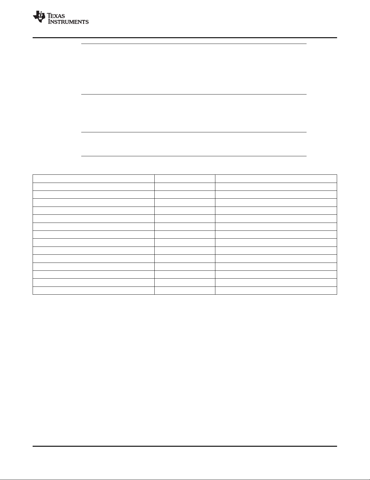
TMS320C6454
www.ti.com
The instructions that write to the PERLOCK and PERCFG0 registers must be in the same
fetch packet if code is being executed from external memory. If the instructions are in
different fetch packets, fetching the second instruction from external memory may stall the
instruction long enough such that PERCFG0 register will be locked before the instruction is
executed.
3.4 Device State Control Registers
The C6454 device has a set of registers that are used to control the status of its peripherals. These
registers are shown in Table 3-5 and described in the next sections.
The device state control registers can only be accessed using the CPU or the emulator.
Table 3-5. Device State Control Registers
HEX ADDRESS RANGE ACRONYM REGISTER NAME
02AC 0000 - Reserved
02AC 0004 PERLOCK Peripheral Lock Register
02AC 0008 PERCFG0 Peripheral Configuration Register 0
02AC 000C - Reserved
02AC 0010 - Reserved
02AC 0014 PERSTAT0 Peripheral Status Register 0
02AC 0018 PERSTAT1 Peripheral Status Register 1
02AC 001C - 02AC 001F - Reserved
02AC 0020 EMACCFG EMAC Configuration Register
02AC 0024 - 02AC 002B - Reserved
02AC 002C PERCFG1 Peripheral Configuration Register 1
02AC 0030 - 02AC 0053 - Reserved
02AC 0054 EMUBUFPD Emulator Buffer Powerdown Register
02AC 0058 - Reserved
SPRS311F–APRIL 2006–REVISED SEPTEMBER 2010
NOTE
NOTE
Copyright © 2006–2010, Texas Instruments Incorporated Device Configuration 57
Submit Documentation Feedback
Product Folder Link(s): TMS320C6454
Page 58

TMS320C6454
SPRS311F–APRIL 2006–REVISED SEPTEMBER 2010
www.ti.com
3.4.1 Peripheral Lock Register Description
When written with correct 32-bit key (0x0F0A0B00), the Peripheral Lock Register (PERLOCK) allows one
write to the PERCFG0 register within 16 SYSCLK3 cycles.
NOTE
The instructions that write to the PERLOCK and PERCFG0 registers must be in the same
fetch packet if code is being executed from external memory. If the instructions are in
different fetch packets, fetching the second instruction from external memory may stall the
instruction long enough such that PERCFG0 register will be locked before the instruction is
executed.
31 0
LOCKVAL
R/W-F0F0 F0F0
LEGEND: R/W = Read/Write; -n = value after reset
Figure 3-3. Peripheral Lock Register (PERLOCK) - 0x02AC 0004
Table 3-6. Peripheral Lock Register (PERLOCK) Field Descriptions
Bit Field Value Description
31:0 LOCKVAL When programmed with 0x0F0A 0B00 allows one write to the PERCFG0 register within 16
SYSCLK3 clock cycles.
58 Device Configuration Copyright © 2006–2010, Texas Instruments Incorporated
Submit Documentation Feedback
Product Folder Link(s): TMS320C6454
Page 59

TMS320C6454
www.ti.com
SPRS311F–APRIL 2006–REVISED SEPTEMBER 2010
3.4.2 Peripheral Configuration Register 0 Description
The Peripheral Configuration Register (PERCFG0) is used to change the state of the peripherals. One
write is allowed to this register within 16 SYSCLK3 cycles after the correct key is written to the PERLOCK
register.
NOTE
The instructions that write to the PERLOCK and PERCFG0 registers must be in the same
fetch packet if code is being executed from external memory. If the instructions are in
different fetch packets, fetching the second instruction from external memory may stall the
instruction long enough that the PERCFG0 register is locked before the instruction is
executed.
31 24
Reserved
R/W-0
23 21 20 19 18 17 16
Reserved PCICTL Reserved HPICTL Reserved McBSP1CTL
R/W-0 R/W-0 R/W-0 R/W-0 R/W-0 R/W-0
15 14 13 12 11 10 9 8
Reserved McBSP0CTL Reserved I2CCTL Reserved GPIOCTL Reserved TIMER1CTL
R/W-0 R/W-0 R/W-0 R/W-0 R/W-0 R/W-0 R/W-0 R/W-0
7 6 5 4 3 0
Reserved TIMER0CTL Reserved EMACCTL Reserved
R/W-0 R/W-0 R/W-0 R/W-0 R/W-0
LEGEND: R/W = Read/Write; -n = value after reset
Figure 3-4. Peripheral Configuration Register 0 (PERCFG0) - 0x02AC 0008
Table 3-7. Peripheral Configuration Register 0 (PERCFG0) Field Descriptions
Bit Field Value Description
31:21 Reserved Reserved.
20 PCICTL Mode control for PCI. This bit defaults to 1 when host boot is used (BOOTMODE[3:0] = 0111b).
0 Set PCI to disabled mode
1 Set PCI to enabled mode
19 Reserved Reserved.
18 HPICTL Mode control for HPI. This bit defaults to 1 when host boot is used (BOOTMODE[3:0] = 0001b).
0 Set HPI to disabled mode
1 Set HPI to enabled mode
17 Reserved 1 Reserved.
16 McBSP1CTL Mode control for McBSP1
0 Set McBSP1 to disabled mode
1 Set McBSP1 to enabled mode
15 Reserved Reserved.
14 McBSP0CTL Mode control for McBSP0
0 Set McBSP0 to disabled mode
1 Set McBSP0 to enabled mode
13 Reserved Reserved.
Copyright © 2006–2010, Texas Instruments Incorporated Device Configuration 59
Submit Documentation Feedback
Product Folder Link(s): TMS320C6454
Page 60

TMS320C6454
SPRS311F–APRIL 2006–REVISED SEPTEMBER 2010
Table 3-7. Peripheral Configuration Register 0 (PERCFG0) Field Descriptions (continued)
Bit Field Value Description
12 I2CCTL Mode control for I2C
0 Set I2C to disabled mode
1 Set I2C to enabled mode
11 Reserved Reserved.
10 GPIOCTL Mode control for GPIO
0 Set GPIO to disabled mode
1 Set GPIO to enabled mode
9 Reserved Reserved.
8 TIMER1CTL Mode control for Timer 1
0 Set Timer 1 to disabled mode
1 Set Timer 1 to enabled mode
7 Reserved Reserved.
6 TIMER0CTL Mode control for Timer 0
0 Set Timer 0 to disabled mode
1 Set Timer 0 to enabled mode
5 Reserved Reserved.
4 EMACCTL Mode control for EMAC/MDIO
0 Set EMAC/MDIO to disabled mode
1 Set EMAC/MDIO to enabled mode
3:0 Reserved Reserved.
www.ti.com
3.4.3 Peripheral Configuration Register 1 Description
The Peripheral Configuration Register (PERCFG1) is used to enable the EMIFA and DDR2 Memory
Controller. EMIFA and the DDR2 Memory Controller do not have corresponding status bits in the
Peripheral Status Registers. The EMIFA and DDR2 Memory Controller peripherals can be used within 16
SYSCLK3 cycles after EMIFACTL and DDR2CTL are set to 1. Once EMIFACTL and DDR2CTL are set to
1, they cannot be set to 0. Note that if the DDR2 Memory Controller and EMIFA are disabled at reset
through the device configuration pins (DDR2.EN[ABA0] and EMIFA[ABA1]), they cannot be enabled
through the PERCFG1 register.
31 8
Reserved
R-0x00
7 2 1 0
Reserved DDR2CTL EMIFACTL
R-0x00 R/W-0 R/W-0
LEGEND: R/W = Read/Write; R = Read only; -n = value after reset
Figure 3-5. Peripheral Configuration Register 1 (PERCFG1) - 0x02AC 002C
Table 3-8. Peripheral Configuration Register 1 (PERCFG1) Field Descriptions
Bit Field Value Description
31:2 Reserved Reserved.
1 DDR2CTL Mode Control for DDR2 Memory Controller. Once this bit is set to 1, it cannot be changed to 0.
0 Set DDR2 to disabled
1 Set DDR2 to enabled
60 Device Configuration Copyright © 2006–2010, Texas Instruments Incorporated
Submit Documentation Feedback
Product Folder Link(s): TMS320C6454
Page 61

TMS320C6454
www.ti.com
SPRS311F–APRIL 2006–REVISED SEPTEMBER 2010
Table 3-8. Peripheral Configuration Register 1 (PERCFG1) Field Descriptions (continued)
Bit Field Value Description
0 EMIFACTL Mode control for EMIFA. Once this bit is set to 1, it cannot be changed to 0. This bit defaults to 1 if
EMIFA 8-bit ROM boot is used (BOOTMODE[3:0] = 0100b).
0 Set EMIFA to disabled
1 Set EMIFA to enabled
Copyright © 2006–2010, Texas Instruments Incorporated Device Configuration 61
Submit Documentation Feedback
Product Folder Link(s): TMS320C6454
Page 62

TMS320C6454
SPRS311F–APRIL 2006–REVISED SEPTEMBER 2010
www.ti.com
3.4.4 Peripheral Status Registers Description
The Peripheral Status Registers (PERSTAT0 and PERSTAT1) show the status of the C6454 device
peripherals.
31 30 29 27 26 24
Reserved HPISTAT McBSP1STAT
R-0 R-0 R-0
23 21 20 18 17 16
McBSP0STAT I2CSTAT GPIOSTAT
R-0 R-0 R-0
15 14 12 11 9 8
GPIOSTAT TIMER1STAT TIMER0STAT EMACSTAT
R-0 R-0 R-0 R-0
7 6 5 0
EMACSTAT Reserved
R-0 R-0
LEGEND: R = Read only; -n = value after reset
Figure 3-6. Peripheral Status Register 0 (PERSTAT0) - 0x02AC 0014
Table 3-9. Peripheral Status Register 0 (PERSTAT0) Field Descriptions
Bit Field Value Description
31:30 Reserved Reserved.
29:27 HPISTAT HPI status
000 HPI is in the disabled state
001 HPI is in the enabled state
011 HPI is in the static powerdown state
100 HPI is in the disable in progress state
101 HPI is in the enable in progress state
Others Reserved
26:24 McBSP1STAT McBSP1 status
000 McBSP1 is in the disabled state
001 McBSP1 is in the enabled state
011 McBSP1 is in the static powerdown state
100 McBSP1 is in the disable in progress state
101 McBSP1 is in the enable in progress state
Others Reserved
23:21 McBSP0STAT McBSP0 status
000 McBSP0 is in the disabled state
001 McBSP0 is in the enabled state
011 McBSP0 is in the static powerdown state
100 McBSP0 is in the disable in progress state
101 McBSP0 is in the enable in progress state
Others Reserved
62 Device Configuration Copyright © 2006–2010, Texas Instruments Incorporated
Submit Documentation Feedback
Product Folder Link(s): TMS320C6454
Page 63

TMS320C6454
www.ti.com
Table 3-9. Peripheral Status Register 0 (PERSTAT0) Field Descriptions (continued)
Bit Field Value Description
20:18 I2CSTAT I2C status
000 I2C is in the disabled state
001 I2C is in the enabled state
011 I2C is in the static powerdown state
100 I2C is in the disable in progress state
101 I2C is in the enable in progress state
Others Reserved
17:15 GPIOSTAT GPIO status
000 GPIO is in the disabled state
001 GPIO is in the enabled state
011 GPIO is in the static powerdown state
100 GPIO is in the disable in progress state
101 GPIO is in the enable in progress state
Others Reserved
14:12 TIMER1STAT Timer1 status
000 Timer1 is in the disabled state
001 Timer1 is in the enabled state
011 Timer1 is in the static powerdown state
100 Timer1 is in the disable in progress state
101 Timer1 is in the enable in progress state
Others Reserved
11:9 TIMER0STAT Timer0 status
000 Timer0 is in the disabled state
001 Timer0 is in the enabled state
011 Timer0 is in the static powerdown state
100 Timer0 is in the disable in progress state
101 Timer0 is in the enable in progress state
Others Reserved
8:6 EMACSTAT EMAC/MDIO status
000 EMAC/MDIO is in the disabled state
001 EMAC/MDIO is in the enabled state
011 EMAC/MDIO is in the static powerdown state
100 EMAC/MDIO is in the disable in progress state
101 EMAC/MDIO is in the enable in progress state
Others Reserved
5:0 Reserved Reserved
SPRS311F–APRIL 2006–REVISED SEPTEMBER 2010
31 16
Reserved
R-0
15 5 3 2 0
Reserved PCISTAT
R-0 R-0
LEGEND: R = Read only; -n = value after reset
Figure 3-7. Peripheral Status Register 1 (PERSTAT1) - 0x02AC 0018
Copyright © 2006–2010, Texas Instruments Incorporated Device Configuration 63
Submit Documentation Feedback
Product Folder Link(s): TMS320C6454
Page 64

TMS320C6454
SPRS311F–APRIL 2006–REVISED SEPTEMBER 2010
Table 3-10. Peripheral Status Register 1 (PERSTAT1) Field Descriptions
Bit Field Value Description
31:3 Reserved Reserved
2:0 PCISTAT PCI status
000 PCI is in the disabled state
001 PCI is in the enabled state
011 PCI is in the static powerdown state
101 PCI is in the enable in progress state
Others Reserved
www.ti.com
64 Device Configuration Copyright © 2006–2010, Texas Instruments Incorporated
Submit Documentation Feedback
Product Folder Link(s): TMS320C6454
Page 65
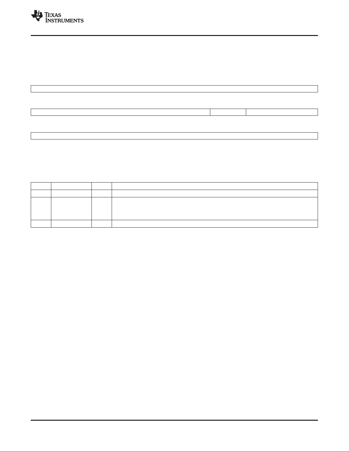
TMS320C6454
www.ti.com
SPRS311F–APRIL 2006–REVISED SEPTEMBER 2010
3.4.5 EMAC Configuration Register (EMACCFG) Description
The EMAC Configuration Register (EMACCFG) is used to assert and deassert the reset of the Reduced
Media Independent Interface (RMII) logic of the EMAC. For more details on how to use this register, see
Section 7.14, Ethernet MAC (EMAC).
31 24
Reserved
R/W-0
23 19 18 17 16
Reserved RMII_RST Reserved
R/W-0001b R/W-1 R/W-0
15 0
Reserved
R/W-0
LEGEND: R/W = Read/Write; R = Read only; -n = value after reset
Figure 3-8. EMAC Configuration Register (EMACCFG) - 0x02AC 0020
Table 3-11. EMAC Configuration Register (EMACCFG) Field Descriptions
Bit Field Value Description
31:19 Reserved Reserved. Writes to this register must keep the default values of these bits.
18 RMII_RST RMII reset bit. This bit is used to reset the RMII logic of the EMAC.
0 RMII logic reset is released.
1 RMII logic reset is asserted.
17:0 Reserved Reserved. Writes to this register must keep this bit as 0.
Copyright © 2006–2010, Texas Instruments Incorporated Device Configuration 65
Submit Documentation Feedback
Product Folder Link(s): TMS320C6454
Page 66

TMS320C6454
SPRS311F–APRIL 2006–REVISED SEPTEMBER 2010
3.4.6 Emulator Buffer Powerdown Register (EMUBUFPD) Description
The Emulator Buffer Powerdown Register (EMUBUFPD) is used to control the state of the pin buffers of
emulator pins EMU[18:2]. These buffers can be powered down if the device trace feature is not needed.
31 8
Reserved
R-0
7 1 0
Reserved EMUCTL
R-0 R/W-0
LEGEND: R/W = Read/Write; R = Read only; -n = value after reset
Figure 3-9. Emulator Buffer Powerdown Register (EMUBUFPD) - 0x02AC 0054
Table 3-12. Emulator Buffer Powerdown Register (EMUBUFPD) Field Descriptions
Bit Field Value Description
31:1 Reserved Reserved
0 EMUCTL Buffer powerdown for EMU[18:2] pins
0 Power-up buffers
1 Power-down buffers
www.ti.com
66 Device Configuration Copyright © 2006–2010, Texas Instruments Incorporated
Submit Documentation Feedback
Product Folder Link(s): TMS320C6454
Page 67

TMS320C6454
www.ti.com
SPRS311F–APRIL 2006–REVISED SEPTEMBER 2010
3.5 Device Status Register Description
The device status register depicts the device configuration selected upon device reset. Once set, these
bits will remain set until a device reset. For the actual register bit names and their associated bit field
descriptions, see Figure 3-10 and Table 3-13.
Note that enabling or disabling peripherals through the Peripheral Configuration Registers (PERCFG0 and
PERCFG1) does not affect the DEVSTAT register. To determine the status of peripherals following writes
to the PERCFG0 and PERCFG1 registers, read the Peripherals Status Registers (PERSTAT0 and
PERSTAT1).
31 24
Reserved
R-0000 0000
23 22 21 20 19 18 17 16
Reserved EMIFA_EN DDR2_EN PCI_EN CFGGP2 CFGGP1 CFGGP0 Reserved
R-0 R-0 R-0 R-0 R-0 R-0 R-0 R-1
15 14 13 12 11 10 9 8
SYSCLKOUT_
EN
R-0 R-0 R-0 R-0 R-0 R-0 R-0 R-1
7 6 5 4 3 2 1 0
Reserved LENDIAN HPI_WIDTH AECLKINSEL BOOTMODE3 BOOTMODE2 BOOTMODE1 BOOTMODE0
R-0 R-1 R-0 R-0 R-0 R-0 R-0 R-0
LEGEND: R/W = Read/Write; R = Read only; -x = value after reset
Note: The default values of the fields in the DEVSTAT register are latched from device configuration pins, as described in Section 3.1,
Device Configuration at Device Reset. The default values shown here correspond to the setting dictated by the internal pullup or pulldown
resistor.
MCBSP1_EN PCI66 Reserved PCI_EEAI MAC_SEL1 MAC_SEL0 Reserved
Figure 3-10. Device Status Register (DEVSTAT) - 0x02A8 0000
Table 3-13. Device Status Register (DEVSTAT) Field Descriptions
Bit Field Value Description
31:23 Reserved Reserved. Read-only, writes have no effect.
22 EMIFA_EN EMIFA Enable (EMIFA_EN) status bit
21 DDR2_EN DDR2 Memory Controller Enable (DDR2_EN) status bit
20 PCI_EN PCI Enable (PCI_EN) status bit
19:17 CFGGP[2:0] Used as General-Purpose inputs for configuration purposes.
16 Reserved Reserved. Read-only, writes have no effect.
15 SYSCLKOUT_EN SYSCLKOUT Enable (SYSCLKOUT_EN) status bit
Shows the status of whether the EMIFA peripheral pins are enabled/disabled.
0 EMIFA peripheral pins are disabled (default)
1 EMIFA peripheral pins are enabled
Shows the status of whether the DDR2 Memory Controller peripheral pins are enabled/disabled.
0 DDR2 Memory Controller peripheral pins are disabled (default)
1 DDR2 Memory Controller peripheral pins are enabled
Shows the status of which function is enabled on the HPI/PCI multiplexed pins.
0 HPI pin functions are enabled (default)
1 PCI pin functions are enabled
These pins are latched at reset. These values can be used by S/W routines for boot operations.
Shows the status of which function is enabled on the SYSCLK4/GP[1] muxed pin.
0 GP[1] pin function of the SYSCLK4/GP[1] pin enabled (default)
1 SYSCLK4 pin function of the SYSCLK4/GP[1] pin enabled
Copyright © 2006–2010, Texas Instruments Incorporated Device Configuration 67
Submit Documentation Feedback
Product Folder Link(s): TMS320C6454
Page 68

TMS320C6454
SPRS311F–APRIL 2006–REVISED SEPTEMBER 2010
Table 3-13. Device Status Register (DEVSTAT) Field Descriptions (continued)
Bit Field Value Description
14 MCBSP1_EN McBSP1 Enable (MCBSP1_EN) status bit
Shows the status of which function is enabled on the McBSP1/GPIO muxed pins.
0 GPIO pin functions enabled (default)
1 McBSP1 pin functions enabled
13 PCI66 PCI Frequency Selection (PCI66) status bit
Shows the PCI operating frequency selected at reset.
0 PCI operates at 33 MHz (default)
1 PCI operates at 66 MHz
11 PCI_EEAI PCI I2C EEPROM Auto-Initialization (PCI_EEAI) status bit
Shows whether the PCI auto-initialization via external I2C EEPROM is enabled/disabled.
0 PCI auto-initialization through external I2C EEPROM is disabled; the PCI peripheral uses the
specified PCI default values (default).
1 PCI auto-initialization through external I2C EEPROM is enabled; the PCI peripheral is configured
through external I2C EEPROM provided the PCI peripheral pin is enabled (PCI_EN = 1).
10:9 MACSEL[1:0] EMAC Interface Select (MACSEL[1:0]) status bits
Shows which EMAC interface mode has been selected.
00 10/100 EMAC/MDIO with MII Interface (default)
01 10/100 EMAC/MDIO with RMII Interface
10 10/100/1000 EMAC/MDIO with GMII Interface
11 10/100/1000 EMAC/MDIO with RGMII Mode Interface
[RGMII interface requires a 1.8-V or 1.5-V I/O supply]
8:7 Reserved Reserved. Read-only, writes have no effect.
6 LENDIAN Device Endian mode (LENDIAN)
Shows the status of whether the system is operating in Big Endian mode or Little Endian mode
(default).
0 System is operating in Big Endian mode
1 System is operating in Little Endian mode (default)
5 HPI_WIDTH HPI bus width control bit.
Shows the status of whether the HPI bus operates in 32-bit mode or in 16-bit mode (default).
0 HPI operates in 16-bit mode. (default)
1 HPI operates in 32-bit mode
4 AECLKINSEL EMIFA input clock select
Shows the status of what clock mode is enabled or disabled for EMIFA.
0 AECLKIN (default mode)
1 SYSCLK4 (CPU/x) Clock Rate. The SYSCLK4 clock rate is software selectable via the PLL1
Controller. By default, SYSCLK4 is selected as CPU/8 clock rate.
3:0 BOOTMODE[3:0] Boot mode configuration bits
Shows the status of what device boot mode configuration is operational.
BOOTMODE[3:0]
[Note: if selected for boot, the corresponding peripheral is automatically enabled after device reset.]
0000 No boot (default mode)
0001 Host boot (HPI)
0010 Reserved
0011 Reserved
0100 EMIFA 8-bit ROM boot
0101 Master I2C boot
0110 Slave I2C boot
0111 Host boot (PCI)
1000 Reserved
thru
1111
For more detailed information on the boot modes, see Section 2.4, Boot Sequence.
www.ti.com
68 Device Configuration Copyright © 2006–2010, Texas Instruments Incorporated
Submit Documentation Feedback
Product Folder Link(s): TMS320C6454
Page 69
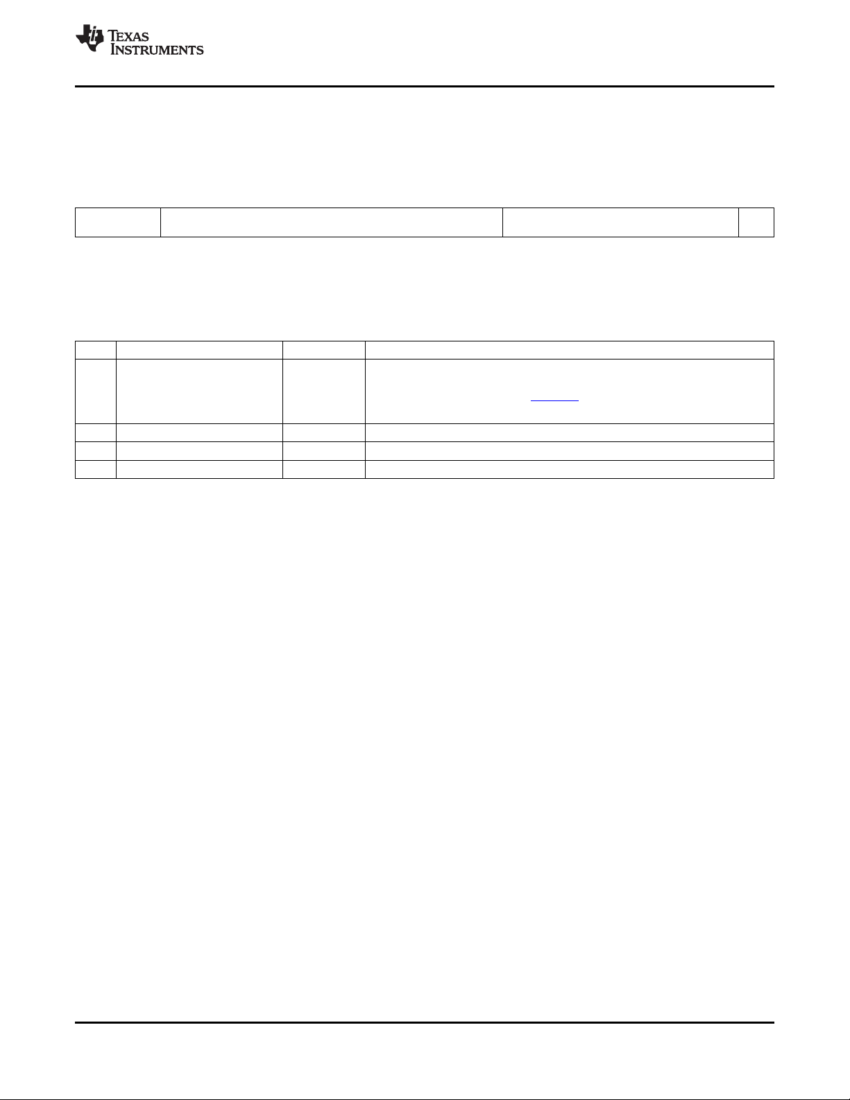
TMS320C6454
www.ti.com
SPRS311F–APRIL 2006–REVISED SEPTEMBER 2010
3.6 JTAG ID (JTAGID) Register Description
The JTAG ID register is a read-only register that identifies to the customer the JTAG/Device ID. For the
C6454 device, the JTAG ID register resides at address location 0x02A8 0008. For the actual register bit
names and their associated bit field descriptions, see Figure 3-11 and Table 3-14.
31 28 27 12 11 1 0
VARIANT PART NUMBER MANUFACTURER
(4-bit) (16-bit) (11-bit)
R-n R-0000 0000 1000 1010b 0000 0010 111b R-1
LEGEND: R = Read only; -n = value after reset
Figure 3-11. JTAG ID (JTAGID) Register - 0x02A8 0008
Table 3-14. JTAG ID (JTAGID) Register Field Descriptions
Bit Field Value Description
31:28 VARIANT Variant (4-Bit) value. The value of this field depends on the silicon revision being
27:12 PART NUMBER Part Number (16-Bit) value. C6454 device value: 0000 0000 1000 1010b.
11:1 MANUFACTURER Manufacturer (11-Bit) value. C6454 device value: 0000 0010 111b.
0 LSB LSB. This bit is read as a "1" for the C6454 device.
used. For more information, see the TMS320C6455/54 Digital Signal Processor
Silicon Errata (literature number SPRZ234).
Note: the VARIANT field may be invalid if no CLKIN1 signal is applied.
LSB
Copyright © 2006–2010, Texas Instruments Incorporated Device Configuration 69
Submit Documentation Feedback
Product Folder Link(s): TMS320C6454
Page 70

TMS320C6454
SPRS311F–APRIL 2006–REVISED SEPTEMBER 2010
3.7 Pullup/Pulldown Resistors
Proper board design should ensure that input pins to the C6454 device always be at a valid logic level and
not floating. This may be achieved via pullup/pulldown resistors. The C6454 device features internal pullup
(IPU) and internal pulldown (IPD) resistors on most pins to eliminate the need, unless otherwise noted, for
external pullup/pulldown resistors.
An external pullup/pulldown resistor needs to be used in the following situations:
• Device Configuration Pins: If the pin is both routed out and 3-stated (not driven), an external
pullup/pulldown resistor must be used, even if the IPU/IPD matches the desired value/state.
• Other Input Pins: If the IPU/IPD does not match the desired value/state, use an external
pullup/pulldown resistor to pull the signal to the opposite rail.
For the device configuration pins (listed in Table 3-1), if they are both routed out and 3-stated (not driven),
it is strongly recommended that an external pullup/pulldown resistor be implemented. Although, internal
pullup/pulldown resistors exist on these pins and they may match the desired configuration value,
providing external connectivity can help ensure that valid logic levels are latched on these device
configuration pins. In addition, applying external pullup/pulldown resistors on the device configuration pins
adds convenience to the user in debugging and flexibility in switching operating modes.
Tips for choosing an external pullup/pulldown resistor:
• Consider the total amount of current that may pass through the pullup or pulldown resistor. Make sure
to include the leakage currents of all the devices connected to the net, as well as any internal pullup or
pulldown resistors.
• Decide a target value for the net. For a pulldown resistor, this should be below the lowest VILlevel of
all inputs connected to the net. For a pullup resistor, this should be above the highest VIHlevel of all
inputs on the net. A reasonable choice would be to target the VOLor VOHlevels for the logic family of
the limiting device; which, by definition, have margin to the VILand VIHlevels.
• Select a pullup/pulldown resistor with the largest possible value; but, which can still ensure that the net
will reach the target pulled value when maximum current from all devices on the net is flowing through
the resistor. The current to be considered includes leakage current plus, any other internal and
external pullup/pulldown resistors on the net.
• For bidirectional nets, there is an additional consideration which sets a lower limit on the resistance
value of the external resistor. Verify that the resistance is small enough that the weakest output buffer
can drive the net to the opposite logic level (including margin).
• Remember to include tolerances when selecting the resistor value.
• For pullup resistors, also remember to include tolerances on the DVDDrail.
www.ti.com
For most systems, a 1-kΩ resistor can be used to oppose the IPU/IPD while meeting the above criteria.
Users should confirm this resistor value is correct for their specific application.
For most systems, a 20-kΩ resistor can be used to compliment the IPU/IPD on the device configuration
pins while meeting the above criteria. Users should confirm this resistor value is correct for their specific
application.
For more detailed information on input current (II), and the low-/high-level input voltages (VILand VIH) for
the C6454 device, see Section 6.3, Electrical Characteristics Over Recommended Ranges of Supply
Voltage and Operating Case Temperature.
To determine which pins on the C6454 device include internal pullup/pulldown resistors, see Table 2-3,
Terminal Functions.
3.8 Configuration Examples
Figure 3-12 and Figure 3-13 illustrate examples of peripheral selections/options that are configurable on
the C6454 device.
70 Device Configuration Copyright © 2006–2010, Texas Instruments Incorporated
Submit Documentation Feedback
Product Folder Link(s): TMS320C6454
Page 71
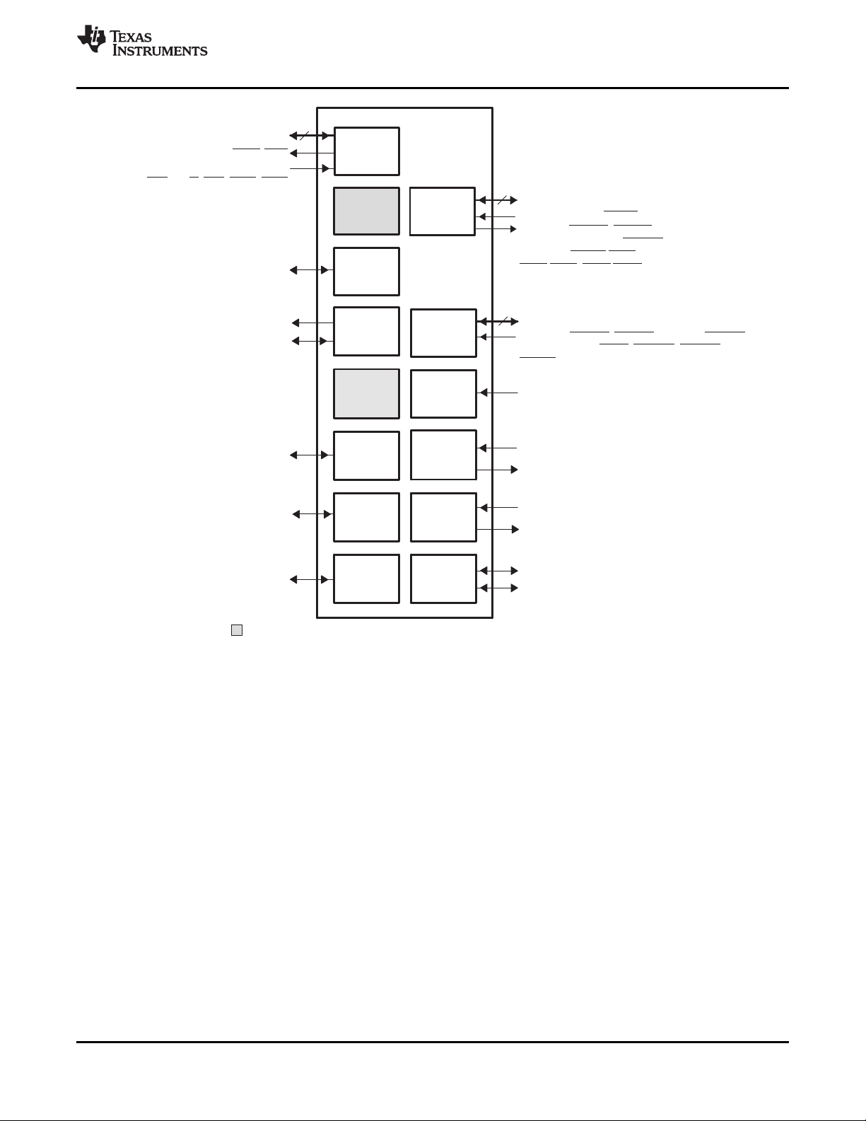
Shading denotes a peripheral module not available for this configuration.
McBSP0
TIMER0
EMIFA
GPIO
PLL2
and PLL2
Controller
TIMER1
PLL1
and PLL1
Controller
DDR2
EMIF
AED[63:0]
64
AECLKIN, AARDY, AHOLD
AEA[22:3], ACE[3:0], ABE[7:0],
AECLKOUT, ASDCKE, AHOLDA
,
ABUSREQ, ASADS
/ASRE,
AAOE
/ASOE, AAWE/ASWE
SCL
SDA
CLKIN1, PLLV1
SYSCLK4
HRDY, HINT
HCNTL0, HCNTL1, HHWIL,
HAS
, HR/W, HCS, HDS1, HDS2
CLKR0, FSR0, DR0, CLKS0,
DX0, FSX0, CLKX0
MRXD[7:0], MRXER, MRXDV, MCOL,
MCRS, MTCLK, MRCLK
32
HD[31:0]
CLKIN2, PLLV2
GP[15:12,2,1]
DEA[21:2], DCE[1:0], DBE[3:0], DDRCLK, DDRCLK,
DSDCKE, DDQS, DDQS
, DSDCAS, DSDRAS,
DSDWE
AEA[19:16] (BOOTMODE[3:0]) = 0001, (HPI Boot)
AEA[15] (AECLKIN_SEL) = 0, (AECLKIN, default)
AEA[14] (HPI_WIDTH) = 1, (HPI, 32-bit Operation)
AEA[13] (LENDIAN) = IPU, (Little Endian Mode, default)
AEA[12] = 0, (do not oppose IPD)
AEA[11] = 0, (do not oppose IPD)
AEA[10:9] (MACSEL[1:0]) = 00, (10/100 MII Mode)
AEA[8] (PCI_EEAI) = 0, (PCI I2C EEPROM Auto-Init disabled, default)
AEA[7] = 0, (do not oppose IPD)
AEA[6] (PCI66) = 0, (PCI 33 MHz [default, don’t care])
AEA[5] (MCBSP1_EN) = 0, (McBSP1 disabled, default)
AEA[4] (SYSCLKOUT_EN) = 1, (SYSCLK4 pin function)
AEA[3] = 0, (do not oppose IPD)
AEA[2:0] (CFGGP[2:0]) = 000, (default)
McBSP1
EMAC
32
ED[31:0]
TINP1L
TOUT1L
TOUT0
TINP0
MTXD[7:0], MTXEN,
MDIO, MDCLK
MDIO
I2C
PCI
HPI
(32-Bit)
DEVSTAT Register: 0x0061 8161
PCI_EN = 0 (PCI disabled, default)
ABA1 (EMIFA_EN) = 1(EMIFA enabled)
ABA0 (DDR2_EN) = 1 (DDR2 Memory Controller enabled)
TMS320C6454
www.ti.com
SPRS311F–APRIL 2006–REVISED SEPTEMBER 2010
Figure 3-12. Configuration Example A (McBSP + HPI32 + I2C + EMIFA + DDR2 Memory Controller +
TIMERS + EMAC (MII) + MDIO)
Copyright © 2006–2010, Texas Instruments Incorporated Device Configuration 71
Submit Documentation Feedback
Product Folder Link(s): TMS320C6454
Page 72
Shading denotes a peripheral module not available for this configuration.
McBSP0
TIMER0
EMIFA
GPIO
TIMER1
PLL1
and PLL1
Controller
DDR2
EMIF
AED[63:0]
64
AECLKIN, AARDY, AHOLD
AEA[22:3], ACE[3:0], ABE[7:0],
AECLKOUT, ASDCKE,
AHOLDA, ABUSREQ,
ASADS
/ASRE, AAOE/ASOE,
AAWE
/ASWE
SCL
SDA
CLKIN1, PLLV1
SYSCLK4
HRDY, HINT
HCNTL0, HCNTL1, HHWIL,
HAS
, HR/W, HCS, HDS1, HDS2
CLKR0, FSR0, DR0, CLKS0,
DX0, FSX0, CLKX0
MRXD[7:0], MRXER, MRXDV, MCOL,
MCRS, MTCLK, MRCLK
32
HD[31:0]
CLKIN2, PLLV2
GP[15:12,2,1]
DEA[21:2], DCE[1:0], DBE[3:0], DDRCLK, DDRCLK,
DSDCKE, DDQS, DDQS
, DSDCAS, DSDRAS,
DSDWE
AEA[19:16] (BOOTMODE[3:0]) = 0001, (HPI Boot)
AEA[15] (AECLKIN_SEL) = 0, (AECLKIN, default)
AEA[14] (HPI_WIDTH) = 1, (HPI, 32-bit Operation)
AEA[13] (LENDIAN) = IPU, (Little Endian Mode, default)
AEA[12] = 0, (do not oppose IPD)
AEA[11] = 0, (do not oppose IPD)
AEA[10:9] (MACSEL[1:0]) = 00, (10/100 MII Mode)
AEA[8] (PCI_EEAI) = 0, (PCI I2C EEPROM Auto-Init disabled, default)
AEA[7] = 0, (do not oppose IPD)
AEA[6] (PCI66) = 0, (PCI 33 MHz [default, don’t care])
AEA[5] (MCBSP1_EN) = 1, (McBSP1 enabled)
AEA[4] (SYSCLKOUT_EN) = 1, (SYSCLK4 pin function)
AEA[3] = 0, (do not oppose IPD)
AEA[2:0] (CFGGP[2:0]) = 000, (default)
McBSP1
EMAC
32
ED[31:0]
TINP1L
TOUT1L
TOUT0
TINP0
MTXD[7:0], MTXEN,
MDIO, MDCLK
MDIO
I2C
PCI
HPI
(32-Bit)
CLKR1, FSR1, DR1, CLKS1,
DX1, FSX1, CLKX1
DEVSTAT Register: 0x0061 C161
PCI_EN = 0 (PCI disabled, default)
ABA1 (EMIFA_EN) = 1(EMIFA enabled)
ABA0 (DDR2_EN) = 1 (DDR2 Memory Controller enabled)
PLL2
and PLL2
Controller
TMS320C6454
SPRS311F–APRIL 2006–REVISED SEPTEMBER 2010
www.ti.com
Figure 3-13. Configuration Example B (2 McBSPs + HPI32 + I2C + EMIFA + DDR2 Memory Controller +
TIMERS + EMAC (GMII) + MDIO
72 Device Configuration Copyright © 2006–2010, Texas Instruments Incorporated
Submit Documentation Feedback
Product Folder Link(s): TMS320C6454
Page 73

TMS320C6454
www.ti.com
4 System Interconnect
On the C6454 device, the C64x+ Megamodule, the EDMA3 transfer controllers, and the system
peripherals are interconnected through two switch fabrics. The switch fabrics allow for low-latency,
concurrent data transfers between master peripherals and slave peripherals. The switch fabrics also allow
for seamless arbitration between the system masters when accessing system slaves.
4.1 Internal Buses, Bridges, and Switch Fabrics
Two types of buses exist in the C6454 device: data buses and configuration buses. Some C6454 device
peripherals have both a data bus and a configuration bus interface, while others only have one type of
interface. Furthermore, the bus interface width and speed varies from peripheral to peripheral.
Configuration buses are mainly used to access the register space of a peripheral and the data buses are
used mainly for data transfers. However, in some cases, the configuration bus is also used to transfer
data. For example, data is transferred to the McBSP via its configuration bus. Similarly, the data bus can
also be used to access the register space of a peripheral. For example, the EMIFA and DDR2 memory
controller registers are accessed through their data bus interface.
The C64x+ Megamodule, the EDMA3 traffic controllers, and the various system peripherals can be
classified into two categories: masters and slaves. Masters are capable of initiating read and write
transfers in the system and do not rely on the EDMA3 for their data transfers. Slaves on the other hand
rely on the EDMA3 to perform transfers to and from them. Masters include the EDMA3 traffic controllers
and PCI. Slaves include the McBSP and I2C.
SPRS311F–APRIL 2006–REVISED SEPTEMBER 2010
The C6454 device contains two switch fabrics through which masters and slaves communicate. The data
switch fabric, known as the data switched central resource (SCR), is a high-throughput interconnect
mainly used to move data across the system (for more information, see Section 4.2). The data SCR
connects masters to slaves via 128-bit data buses running at a SYSCLK2 frequency (SYSCLK2 is
generated from PLL1 controller). Peripherals that have a 128-bit data bus interface running at this speed
can connect directly to the data SCR; other peripherals require a bridge.
The configuration switch fabric, also known as the configuration switch central resource (SCR) is mainly
used by the C64x+ Megamodule to access peripheral registers (for more information, see Section 4.3).
The configuration SCR connects C64x+ Megamodule to slaves via 32-bit configuration buses running at a
SYSCLK2 frequency (SYSCLK2 is generated from PLL1 controller). As with the data SCR, some
peripherals require the use of a bridge to interface to the configuration SCR. Note that the data SCR also
connects to the configuration SCR.
Bridges perform a variety of functions:
• Conversion between configuration bus and data bus.
• Width conversion between peripheral bus width and SCR bus width.
• Frequency conversion between peripheral bus frequency and SCR bus frequency.
For example, the EMIFA and DDR2 memory controller require a bridge to convert their 64-bit data bus
interface into a 128-bit interface so that they can connect to the data SCR.
Note that some peripherals can be accessed through the data SCR and also through the configuration
SCR.
Copyright © 2006–2010, Texas Instruments Incorporated System Interconnect 73
Submit Documentation Feedback
Product Folder Link(s): TMS320C6454
Page 74

TMS320C6454
SPRS311F–APRIL 2006–REVISED SEPTEMBER 2010
4.2 Data Switch Fabric Connections
Figure 4-1 shows the connection between slaves and masters through the data switched central resource
(SCR). Masters are shown on the right and slaves on the left. The data SCR connects masters to slaves
via 128-bit data buses running at a SYSCLK2 frequency. SYSCLK2 is supplied by the PLL1 controller and
is fixed at a frequency equal to the CPU frequency divided by 3.
Some peripherals, like PCI and the C64x+ Megamodule, have both slave and master ports. Note that
each EDMA3 transfer controller has an independent connection to the data SCR.
Note that masters can access the configuration SCR through the data SCR. The configuration SCR is
described in Section 4.3.
Not all masters on the C6454 DSP may connect to all slaves. Allowed connections are summarized in
Table 4-1.
www.ti.com
74 System Interconnect Copyright © 2006–2010, Texas Instruments Incorporated
Submit Documentation Feedback
Product Folder Link(s): TMS320C6454
Page 75

EMAC
HPI
M
M
128-bit
(SYSCLK2)
M3
M0
S
M
M
M
McBSPsS
DDR2
Memory
Controller
S
EMIFAS
PCI
S
MASTER
SM
Bridge
CFG
SCR
S
Bridge
PCI M
EDMA3 Channel
Controller
EDMA3
Transfer
Controllers
Megamodule
M1
M2
S3
S0
S1
S2
S S
Events
MMegamodule
Data SCR
128 (SYSCLK2)
128 (SYSCLK2)
128 (SYSCLK2)
128 (SYSCLK2)
32 (SYSCLK3)
32
(SYSCLK3)
32 (SYSCLK3)
32
(SYSCLK3)
128 (SYSCLK2)
128 (SYSCLK2)
Bridge
128
(SYSCLK3)
Bridge
Bridge
128
(SYSCLK2)
128
(SYSCLK2)
64
(SYSCLK2)
64
(SYSCLK2)
32 (SYSCLK2)
Configuration Bus
Data Bus
128
(SYSCLK2)
M
32 (SYSCLK3)
128 (SYSCLK2)
32
(SYSCLK3)
32 (SYSCLK3)
TMS320C6454
www.ti.com
SPRS311F–APRIL 2006–REVISED SEPTEMBER 2010
Figure 4-1. Switched Central Resource Block Diagram
Copyright © 2006–2010, Texas Instruments Incorporated System Interconnect 75
Submit Documentation Feedback
Product Folder Link(s): TMS320C6454
Page 76

TMS320C6454
SPRS311F–APRIL 2006–REVISED SEPTEMBER 2010
Table 4-1. SCR Connection Matrix
McBSPs CONFIGURATION SCR PCI EMIFA MEGAMODULE
TC0 N N N Y Y Y
TC1 Y Y Y Y Y Y
TC2 N N Y Y Y Y
TC3 N N Y Y Y Y
EMAC N N N Y Y Y
HPI N Y N Y Y Y
PCI N Y N Y Y Y
DDR2 MEMORY
CONTROLLER
4.3 Configuration Switch Fabric
Figure 4-2 shows the connection between the C64x+ Megamodule and the configuration switched central
resource (SCR). The configuration SCR is mainly used by the C64x+ Megamodule to access peripheral
registers. The data SCR also has a connection to the configuration SCR which allows masters to access
most peripheral registers. The only registers not accessible by the data SCR through the configuration
SCR are the device configuration registers and the PLL1 and PLL2 controller registers; these can only be
accessed by the C64x+ Megamodule.
The configuration SCR uses 32-bit configuration buses running at SYSCLK2 frequency. SYSCLK2 is
supplied by the PLL1 controller and is fixed at a frequency equal to the CPU frequency divided by 3.
www.ti.com
76 System Interconnect Copyright © 2006–2010, Texas Instruments Incorporated
Submit Documentation Feedback
Product Folder Link(s): TMS320C6454
Page 77

Megamodule
M
CFG SCR
S
M
McBSPs
S
Timers
S
HPI
S
PCI
S
S
Bridge
7
GPIO
S
EMAC/MDIO
M
Data SCR
S
S
I2C
SS
PLL
Controllers
(A)
S
S
Device
Configuration
Registers
(A)
EDMA3 TC0
S
EDMA3 TC1
S
S EDMA3 TC2
S
EDMA3 CC
SS
EDMA3 TC3
S
M
32
(SYSCLK3)
MUX
32
(SYSCLK2)
32
(SYSCLK2)
32 (SYSCLK2)
32
(SYSCLK3)
32 (SYSCLK2)
32 (SYSCLK2)
32-bit
(SYSCLK2)
Configuration Bus
Data Bus
MUX
32
(SYSCLK2)
32
(SYSCLK2)
32
(SYSCLK2)
32
(SYSCLK2)
A. Only accessible by the C64x+ Megamodule.
B. All clocks in this figure are generated by the PLL1 controller.
32
(SYSCLK3)
32
(SYSCLK3)
32
(SYSCLK3)
32
(SYSCLK3)
32
(SYSCLK3)
32
(SYSCLK3)
32
(SYSCLK3)
32
(SYSCLK3)
TMS320C6454
www.ti.com
SPRS311F–APRIL 2006–REVISED SEPTEMBER 2010
4.4 Bus Priorities
On the C6454 device, bus priority is programmable for each master. The register bit fields and default
Figure 4-2. C64x+ Megamodule - SCR Connection
Copyright © 2006–2010, Texas Instruments Incorporated System Interconnect 77
Submit Documentation Feedback
Product Folder Link(s): TMS320C6454
Page 78

TMS320C6454
SPRS311F–APRIL 2006–REVISED SEPTEMBER 2010
priority levels for C6454 bus masters are shown in Table 4-2. The priority levels should be tuned to obtain
the best system performance for a particular application. Lower values indicate higher priorities. For some
masters, the priority values are programmed at the system level by configuring the PRI_ALLOC register.
Details on the PRI_ALLOC register are shown in Figure 4-3. The C64x+ megamodule and EDMA masters
contain registers that control their own priority values.
The priority is enforced when several masters in the system are vying for the same endpoint. Note that the
configuration SCR port on the data SCR is considered a single endpoint meaning priority will be enforced
when multiple masters try to access the configuration SCR. Priority is also enforced on the configuration
SCR side when a master (through the data SCR) tries to access the same endpoint as the C64x+
megamodule.
In the PRI_ALLOC register, the HOST field applies to the priority of the HPI and PCI peripherals. The
EMAC field specifies the priority of the EMAC peripheral.
Table 4-2. C6454 Default Bus Master Priorities
BUS MASTER PRIORITY CONTROL
EDMA3TC0 0 QUEPRI.PRIQ0 (EDMA3 register)
EDMA3TC1 0 QUEPRI.PRIQ1 (EDMA3 register)
EDMA3TC2 0 QUEPRI.PRIQ2 (EDMA3 register)
EDMA3TC3 0 QUEPRI.PRIQ3 (EDMA3 register)
EMAC 1 PRI_ALLOC.EMAC
PCI 2 PRI_ALLOC.HOST
HPI 2 PRI_ALLOC.HOST
C64x+ Megamodule (MDMA port) 7 MDMAARBE.PRI (C64x+ Megamodule
www.ti.com
DEFAULT
PRIORITY LEVEL
Register)
31 16
Reserved
R-0000 0000 0000 0000
15 12 11 9 8 6 5 3 2 0
Reserved Reserved Reserved HOST EMAC
R-000 0 R/W-001 R-100 R/W-010 R/W-001
LEGEND: R/W = Read/Write; R = Read only; -n = value at reset
Figure 4-3. Priority Allocation Register (PRI_ALLOC)
78 System Interconnect Copyright © 2006–2010, Texas Instruments Incorporated
Submit Documentation Feedback
Product Folder Link(s): TMS320C6454
Page 79

A register file
Data path 1 Data path 2
B register file
D2 S2
xx
xx
M2
L2
Instruction decode
M1
xx
xx
L1 S1 D1
16/32−bit instruction dispatch
Instruction fetch
SPLOOP buffer
64 64
C64x+ CPU
256
32
L1D cache/SRAM
Bandwidth management
Memory protection
L1 data memory controller
IDMA
256
256
Bandwidth management
L1 program memory controller
Memory protection
256
Advanced event
triggering
(AET)
Interrupt
and exception
controller
Power control
L2 memory
controller
256
256
Master DMA
Slave DMA
128
256
L1P cache/SRAM
L2
cache/
SRAM
256
128
128
To primary
switch fabric
Cache
control
Bandwidth
management
Memory
protection
Cache control
Cache control
Internal
ROM
(A)
256
Configuration
Registers
32
To Chip
registers
External memory
controller
A. When accessing the internal ROM of the DSP, the CPU frequency must always be less than 750 MHz.
TMS320C6454
www.ti.com
5 C64x+ Megamodule
The C64x+ Megamodule consists of several components — the C64x+ CPU, the L1 program and data
memory controllers, the L2 memory controller, the internal DMA (IDMA), the interrupt controller,
power-down controller, and external memory controller. The C64x+ Megamodule also provides support for
memory protection (for L1P, L1D, and L2 memories) and bandwidth management (for resources local to
the C64x+ Megamodule). Figure 5-1 shows a block diagram of the C64x+ Megamodule.
SPRS311F–APRIL 2006–REVISED SEPTEMBER 2010
5.1 Memory Architecture
For more detailed information on the TMS320C64x+ Megamodule on the C6454 device, see the
TMS320C64x+ Megamodule Reference Guide (literature number SPRU871).
The TMS320C6454 device contains a 1024KB level-2 memory (L2), a 32KB level-1 program memory
(L1P), and a 32KB level-1 data memory (L1D).
The L1P memory configuration for the C6454 device is as follows:
• Region 0 size is 0K bytes (disabled).
• Region 1 size is 32K bytes with no wait states.
The L1D memory configuration for the C6454 device is as follows:
• Region 0 size is 0K bytes (disabled).
Figure 5-1. 64x+ Megamodule Block Diagram
• Region 1 size is 32K bytes with no wait states.
Copyright © 2006–2010, Texas Instruments Incorporated C64x+ Megamodule 79
Submit Documentation Feedback
Product Folder Link(s): TMS320C6454
Page 80
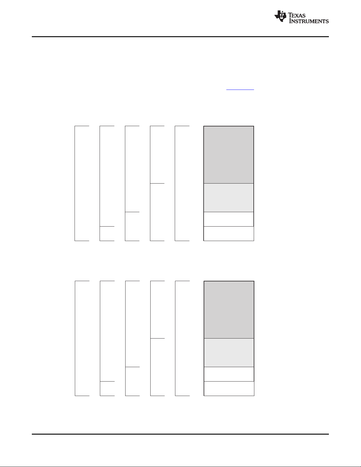
4K bytes
8K bytes
16K bytes
L1P memory
00E0 0000h
00E0 4000h
00E0 6000h
00E0 7000h
00E0 8000h
direct
mapped
SRAM
1/2
dm
3/4
SRAM
SRAM
7/8
All
SRAM
000 001 010 011 100
Block base
address
L1P mode bits
cache
4K bytes
cache
direct
mapped
cache
direct
mapped
cache
4K bytes
8K bytes
16K bytes
L1D memory
00F0 0000h
00F0 4000h
00F0 6000h
00F0 7000h
00F0 8000h
2-way
SRAM
1/2
2-way
3/4
SRAM
SRAM
7/8
All
SRAM
000 001 010 011 100
Block base
address
L1D mode bits
cache
4K bytes
cache
2-way
cache
2-way
cache
TMS320C6454
SPRS311F–APRIL 2006–REVISED SEPTEMBER 2010
L1D is a two-way set-associative cache while L1P is a direct-mapped cache.
The L1P and L1D cache can be reconfigured via software through the L1PMODE field of the L1P
Configuration Register (L1PMODE) and the L1DMODE field of the L1D Configuration Register (L1DCFG)
of the C64x+ Megamodule. After device reset, L1P and L1D cache are configured as all cache or all
SRAM. The on-chip Bootloader changes the reset configuration for L1P and L1D. For more information,
see the TMS320C645x Bootloader User's Guide (literature number SPRUEC6).
Figure 5-2 and Figure 5-3 show the available SRAM/cache configurations for L1P and L1D, respectively.
www.ti.com
Figure 5-2. TMS320C6454 L1P Memory Configurations
Figure 5-3. TMS320C6454 L1D Memory Configurations
The L2 memory configuration for the C6454 device is as follows:
• Port 0 configuration:
80 C64x+ Megamodule Copyright © 2006–2010, Texas Instruments Incorporated
Submit Documentation Feedback
Product Folder Link(s): TMS320C6454
Page 81

32K bytes
32K bytes
64K bytes
128K bytes
792K bytes
L2 memory
0080 0000h
008C 0000h
008E 0000h
008F 0000h
008F 8000h
0090 0000h
3/4
SRAM
4-way
cache
4-way
cache
7/8
SRAM
4-way
cache
15/16
SRAM
4-way
31/32
SRAM
All
SRAM
000 001 010 011 111
Block base
address
L2 mode bits
TMS320C6454
www.ti.com
• Port 1 configuration:
L2 memory can be configured as all SRAM or as part 4-way set-associative cache. The amount of L2
memory that is configured as cache is controlled through the L2MODE field of the L2 Configuration
Register (L2CFG) of the C64x+ Megamodule. Figure 5-4 shows the available SRAM/cache configurations
for L2. By default, L2 is configured as all SRAM after device reset.
SPRS311F–APRIL 2006–REVISED SEPTEMBER 2010
– Memory size is 1024KB
– Starting address is 0080 0000h
– 2-cycle latency
– 4 × 128-bit bank configuration
– Memory size is 32K bytes (this corresponds to the internal ROM)
– Starting address is 0010 0000h
– 1-cycle latency
– 1 × 256-bit bank configuration
For more information on the operation L1 and L2 caches, see the TMS320C64x+ DSP Cache User's
Guide (literature number SPRU862).
All memory on the C6454 device has a unique location in the memory map (see Table 2-2).
When accessing the internal ROM of the DSP, the CPU frequency must always be less than 750 MHz.
Therefore, when using a software boot mode, care must be taken such that the CPU frequency does not
exceed 750 MHz at any point during the boot sequence. After the boot sequence has completed, the CPU
frequency can be programmed to the frequency required by the application. For more detailed information
ont he boot modes, see Section 2.4, Boot Sequence.
5.2 Memory Protection
Memory protection allows an operating system to define who or what is authorized to access L1D, L1P,
and L2 memory. To accomplish this, the L1D, L1P, and L2 memories are divided into pages. There are 16
pages of L1P (2KB each), 16 pages of L1D (2KB each), and 16 pages of L2 (64KB each). The L1D, L1P,
and L2 memory controllers in the C64x+ Megamodule are equipped with a set of registers that specify the
permissions for each memory page.
Copyright © 2006–2010, Texas Instruments Incorporated C64x+ Megamodule 81
Figure 5-4. TMS320C6454 L2 Memory Configurations
Submit Documentation Feedback
Product Folder Link(s): TMS320C6454
Page 82
TMS320C6454
SPRS311F–APRIL 2006–REVISED SEPTEMBER 2010
Each page may be assigned with fully orthogonal user and supervisor read, write, and execute
permissions. Additionally, a page may be marked as either (or both) locally or globally accessible. A local
access is a direct CPU access to L1D, L1P, and L2, while a global access is initiated by a DMA (either
IDMA or the EDMA3) or by other system masters. Note that EDMA or IDMA transfers programmed by the
CPU count as global accesses.
The CPU and the system masters on the C6454 device are all assigned a privilege ID of 0. Therefore it is
only possible to specify whether memory pages are locally or globally accessible. The AID0 and LOCAL
bits of the memory protection page attribute registers specify the memory page protection scheme, see
Table 5-1.
Table 5-1. Available Memory Page Protection Schemes
AID0 Bit LOCAL Bit Description
0 0 No access to memory page is permitted.
0 1 Only direct access by CPU is permitted.
1 0 Only accesses by system masters and IDMA are permitted (includes EDMA and IDMA
1 1 All accesses permitted
For more information on memory protection for L1D, L1P, and L2, see the TMS320C64x+ Megamodule
Reference Guide (literature number SPRU871).
5.3 Bandwidth Management
www.ti.com
accesses initiated by the CPU).
When multiple requestors contend for a single C64x+ Megamodule resource, the conflict is solved by
granting access to the highest priority requestor. The following four resources are managed by the
Bandwidth Management control hardware:
• Level 1 Program (L1P) SRAM/Cache
• Level 1 Data (L1D) SRAM/Cache
• Level 2 (L2) SRAM/Cache
• Memory-mapped registers configuration bus
The priority level for operations initiated within the C64x+ Megamodule; e.g., CPU-initiated transfers,
user-programmed cache coherency operations, and IDMA-initiated transfers, are declared through
registers in the C64x+ Megamodule. The priority level for operations initiated outside the C64x+
Megamodule by system peripherals is declared through the Priority Allocation Register (PRI_ALLOC), see
Section 4.4. System peripherals with no fields in PRI_ALLOC have their own registers to program their
priorities.
More information on the bandwidth management features of the C64x+ Megamodule can be found in the
TMS320C64x+ Megamodule Reference Guide (literature number SPRU871).
82 C64x+ Megamodule Copyright © 2006–2010, Texas Instruments Incorporated
Submit Documentation Feedback
Product Folder Link(s): TMS320C6454
Page 83
TMS320C6454
www.ti.com
5.4 Power-Down Control
The C64x+ Megamodule supports the ability to power-down various parts of the C64x+ Megamodule. The
power-down controller (PDC) of the C64x+ Megamodule can be used to power down L1P, the cache
control hardware, the CPU, and the entire C64x+ Megamodule. These power-down features can be used
to design systems for lower overall system power requirements.
The C6454 device does not support power-down modes for the L2 memory at this time.
More information on the power-down features of the C64x+ Megamodule can be found in the
TMS320C64x+ Megamodule Reference Guide (literature number SPRU871).
5.5 Megamodule Resets
Table 5-2 shows the reset types supported on the C6454 device and they affect the resetting of the
Megamodule, either both globally or just locally.
Power-On Reset Y Y
Warm Reset Y Y
System Reset Y Y
CPU Reset N Y
SPRS311F–APRIL 2006–REVISED SEPTEMBER 2010
NOTE
Table 5-2. Megamodule Reset (Global or Local)
GLOBAL LOCAL
RESET TYPE MEGAMODULE MEGAMODULE
RESET RESET
For more detailed information on the global and local megamodule resets, see the TMS320C64x+
Megamodule Reference Guide (literature number SPRU871) and for more detailed information on device
resets, see Section 7.6, Reset Controller.
Copyright © 2006–2010, Texas Instruments Incorporated C64x+ Megamodule 83
Submit Documentation Feedback
Product Folder Link(s): TMS320C6454
Page 84
TMS320C6454
SPRS311F–APRIL 2006–REVISED SEPTEMBER 2010
www.ti.com
5.6 Megamodule Revision
The version and revision of the C64x+ Megamodule can be read from the Megamodule Revision ID
Register (MM_REVID) located at address 0181 2000h. The MM_REVID register is shown in Figure 5-5
and described in Table 5-3. The C64x+ Megamodule revision is dependant on the silicon revision being
used. For more information, see the TMS320C6455/54 Digital Signal Processor Silicon Errata (literature
number SPRZ234).
31 16 15 0
VERSION REVISION
R-1h R-n
LEGEND: R = Read only; -n = value after reset
A. The C64x+ Megamodule revision is dependant on the silicon revision being used. For more information, see
the TMS320C6455/54 Digital Signal Processor Silicon Errata (literature number SPRZ234).
Figure 5-5. Megamodule Revision ID Register (MM_REVID) [Hex Address: 0181 2000h]
Table 5-3. Megamodule Revision ID Register (MM_REVID) Field Descriptions
Bit Field Value Description
31:16 VERSION 1h Version of the C64x+ Megamodule implemented on the device. This field is always read as 1h.
15:0 REVISION Revision of the C64x+ Megamodule version implemented on the device. The C64x+ Megamodule
revision is dependant on the silicon revision being used. For more information, see the
TMS320C6455/54 Digital Signal Processor Silicon Errata (literature number SPRZ234).
(A)
84 C64x+ Megamodule Copyright © 2006–2010, Texas Instruments Incorporated
Submit Documentation Feedback
Product Folder Link(s): TMS320C6454
Page 85
TMS320C6454
www.ti.com
SPRS311F–APRIL 2006–REVISED SEPTEMBER 2010
5.7 C64x+ Megamodule Register Descriptions
Table 5-4. Megamodule Interrupt Registers
HEX ADDRESS RANGE ACRONYM REGISTER NAME
0180 0000 EVTFLAG0 Event Flag Register 0 (Events [31:0])
0180 0004 EVTFLAG1 Event Flag Register 1
0180 0008 EVTFLAG2 Event Flag Register 2
0180 000C EVTFLAG3 Event Flag Register 3
0180 0010 - 0180 001C - Reserved
0180 0020 EVTSET0 Event Set Register 0 (Events [31:0])
0180 0024 EVTSET1 Event Set Register 1
0180 0028 EVTSET2 Event Set Register 2
0180 002C EVTSET3 Event Set Register 3
0180 0030 - 0180 003C - Reserved
0180 0040 EVTCLR0 Event Clear Register 0 (Events [31:0])
0180 0044 EVTCLR1 Event Clear Register 1
0180 0048 EVTCLR2 Event Clear Register 2
0180 004C EVTCLR3 Event Clear Register 3
0180 0050 - 0180 007C - Reserved
0180 0080 EVTMASK0 Event Mask Register 0 (Events [31:0])
0180 0084 EVTMASK1 Event Mask Register 1
0180 0088 EVTMASK2 Event Mask Register 2
0180 008C EVTMASK3 Event Mask Register 3
0180 0090 - 0180 009C - Reserved
0180 00A0 MEVTFLAG0 Masked Event Flag Status Register 0 (Events [31:0])
0180 00A4 MEVTFLAG1 Masked Event Flag Status Register 1
0180 00A8 MEVTFLAG2 Masked Event Flag Status Register 2
0180 00AC MEVTFLAG3 Masked Event Flag Status Register 3
0180 00B0 - 0180 00BC - Reserved
0180 00C0 EXPMASK0 Exception Mask Register 0 (Events [31:0])
0180 00C4 EXPMASK1 Exception Mask Register 1
0180 00C8 EXPMASK2 Exception Mask Register 2
0180 00CC EXPMASK3 Exception Mask Register 3
0180 00D0 - 0180 00DC - Reserved
0180 00E0 MEXPFLAG0 Masked Exception Flag Register 0
0180 00E4 MEXPFLAG1 Masked Exception Flag Register 1
0180 00E8 MEXPFLAG2 Masked Exception Flag Register 2
0180 00EC MEXPFLAG3 Masked Exception Flag Register 3
0180 00F0 - 0180 00FC - Reserved
0180 0100 - Reserved
0180 0104 INTMUX1 Interrupt Multiplexor Register 1
0180 0108 INTMUX2 Interrupt Multiplexor Register 2
0180 010C INTMUX3 Interrupt Multiplexor Register 3
0180 0110 - 0180 013C - Reserved
0180 0140 AEGMUX0 Advanced Event Generator Mux Register 0
0180 0144 AEGMUX1 Advanced Event Generator Mux Register 1
0180 0148 - 0180 017C - Reserved
0180 0180 INTXSTAT Interrupt Exception Status Register
0180 0184 INTXCLR Interrupt Exception Clear Register
Copyright © 2006–2010, Texas Instruments Incorporated C64x+ Megamodule 85
Submit Documentation Feedback
Product Folder Link(s): TMS320C6454
Page 86
TMS320C6454
SPRS311F–APRIL 2006–REVISED SEPTEMBER 2010
Table 5-4. Megamodule Interrupt Registers (continued)
HEX ADDRESS RANGE ACRONYM REGISTER NAME
0180 0188 INTDMASK Dropped Interrupt Mask Register
0180 0188 - 0180 01BC - Reserved
0180 01C0 EVTASRT Event Asserting Register
0180 01C4 - 0180 FFFF - Reserved
Table 5-5. Megamodule Powerdown Control Registers
HEX ADDRESS RANGE ACRONYM REGISTER NAME
0181 0000 PDCCMD Power-down controller command register
0181 0004 - 0181 1FFF - Reserved
Table 5-6. Megamodule Revision Register
HEX ADDRESS RANGE ACRONYM REGISTER NAME
0181 2000 MM_REVID Megamodule Revision ID Register
0181 2004 - 0181 2FFF - Reserved
Table 5-7. Megamodule IDMA Registers
HEX ADDRESS RANGE ACRONYM REGISTER NAME
0182 0000 IDMA0STAT IDMA Channel 0 Status Register
0182 0004 IDMA0MASK IDMA Channel 0 Mask Register
0182 0008 IMDA0SRC IDMA Channel 0 Source Address Register
0182 000C IDMA0DST IDMA Channel 0 Destination Address Register
0182 0010 IDMA0CNT IDMA Channel 0 Count Register
0182 0014 - 0182 00FC - Reserved
0182 0100 IDMA1STAT IDMA Channel 1 Status Register
0182 0104 - Reserved
0182 0108 IMDA1SRC IDMA Channel 1 Source Address Register
0182 010C IDMA1DST IDMA Channel 1 Destination Address Register
0182 0110 IDMA1CNT IDMA Channel 1 Count Register
0182 0114 - 0182 017C - Reserved
0182 0180 - Reserved
0182 0184 - 0182 01FF - Reserved
www.ti.com
86 C64x+ Megamodule Copyright © 2006–2010, Texas Instruments Incorporated
Submit Documentation Feedback
Product Folder Link(s): TMS320C6454
Page 87
TMS320C6454
www.ti.com
SPRS311F–APRIL 2006–REVISED SEPTEMBER 2010
Table 5-8. Megamodule Cache Configuration Registers
HEX ADDRESS RANGE ACRONYM REGISTER NAME
0184 0000 L2CFG L2 Cache Configuration Register
0184 0004 - 0184 001F - Reserved
0184 0020 L1PCFG L1P Configuration Register
0184 0024 L1PCC L1P Cache Control Register
0184 0028 - 0184 003F - Reserved
0184 0040 L1DCFG L1D Configuration Register
0184 0044 L1DCC L1D Cache Control Register
0184 0048 - 0184 0FFF - Reserved
0184 1000 - 0184 104F - See Table 5-10, CPU Megamodule Bandwidth Management Registers
0184 1050 - 0184 3FFF - Reserved
0184 4000 L2WBAR L2 Writeback Base Address Register - for Block Writebacks
0184 4004 L2WWC L2 Writeback Word Count Register
0184 4008 - 0184 400C - Reserved
0184 4010 L2WIBAR L2 Writeback and Invalidate Base Address Register - for Block Writebacks
0184 4014 L2WIWC L2 Writeback and Invalidate word count register
0184 4018 L2IBAR L2 Invalidate Base Address Register
0184 401C L2IWC L2 Invalidate Word Count Register
0184 4020 L1PIBAR L1P Invalidate Base Address Register
0184 4024 L1PIWC L1P Invalidate Word Count Register
0184 4030 L1DWIBAR L1D Writeback and Invalidate Base Address Register
0184 4034 L1DWIWC L1D Writeback and Invalidate Word Count Register
0184 4038 - Reserved
0184 4040 L1DWBAR L1D Writeback Base Address Register - for Block Writebacks
0184 4044 L1DWWC L1D Writeback Word Count Register
0184 4048 L1DIBAR L1D Invalidate Base Address Register
0184 404C L1DIWC L1D Invalidate Word Count Register
0184 4050 - 0184 4FFF - Reserved
0184 5000 L2WB L2 Global Writeback Register
0184 5004 L2WBINV L2 Global Writeback and Invalidate Register
0184 5008 L2INV L2 Global Invalidate Register
0184 500C - 0184 5024 - Reserved
0184 5028 L1PINV L1P Global Invalidate Register
0184 502C - 0184 503C - Reserved
0184 5040 L1DWB L1D Global Writeback Register
0184 5044 L1DWBINV L1D Global Writeback and Invalidate Register
0184 5048 L1DINV L1D Global Invalidate Register
0184 504C - 0184 7FFF - Reserved
0184 8000 - 0184 81FC Reserved
0184 8200 - 0184 823C Reserved
0184 8240 - 0184 827C Reserved
0184 8280 MAR160 Controls EMIFA CE2 Range A000 0000 - A0FF FFFF
0184 8284 MAR161 Controls EMIFA CE2 Range A100 0000 - A1FF FFFF
0184 8288 MAR162 Controls EMIFA CE2 Range A200 0000 - A2FF FFFF
0184 828C MAR163 Controls EMIFA CE2 Range A300 0000 - A3FF FFFF
0184 8290 MAR164 Controls EMIFA CE2 Range A400 0000 - A4FF FFFF
MAR0 to
MAR127
MAR128 to
MAR143
MAR144 to
MAR159
Copyright © 2006–2010, Texas Instruments Incorporated C64x+ Megamodule 87
Submit Documentation Feedback
Product Folder Link(s): TMS320C6454
Page 88
TMS320C6454
SPRS311F–APRIL 2006–REVISED SEPTEMBER 2010
Table 5-8. Megamodule Cache Configuration Registers (continued)
HEX ADDRESS RANGE ACRONYM REGISTER NAME
0184 8294 MAR165 Controls EMIFA CE2 Range A500 0000 - A5FF FFFF
0184 8298 MAR166 Controls EMIFA CE2 Range A600 0000 - A6FF FFFF
0184 829C MAR167 Controls EMIFA CE2 Range A700 0000 - A7FF FFFF
0184 82A0 MAR168 Controls EMIFA CE2 Range A800 0000 - A8FF FFFF
0184 82A4 MAR169 Controls EMIFA CE2 Range A900 0000 - A9FF FFFF
0184 82A8 MAR170 Controls EMIFA CE2 Range AA00 0000 - AAFF FFFF
0184 82AC MAR171 Controls EMIFA CE2 Range AB00 0000 - ABFF FFFF
0184 82B0 MAR172 Controls EMIFA CE2 Range AC00 0000 - ACFF FFFF
0184 82B4 MAR173 Controls EMIFA CE2 Range AD00 0000 - ADFF FFFF
0184 82B8 MAR174 Controls EMIFA CE2 Range AE00 0000 - AEFF FFFF
0184 82BC MAR175 Controls EMIFA CE2 Range AF00 0000 - AFFF FFFF
0184 82C0 MAR176 Controls EMIFA CE3 Range B000 0000 - B0FF FFFF
0184 82C4 MAR177 Controls EMIFA CE3 Range B100 0000 - B1FF FFFF
0184 82C8 MAR178 Controls EMIFA CE3 Range B200 0000 - B2FF FFFF
0184 82CC MAR179 Controls EMIFA CE3 Range B300 0000 - B3FF FFFF
0184 82D0 MAR180 Controls EMIFA CE3 Range B400 0000 - B4FF FFFF
0184 82D4 MAR181 Controls EMIFA CE3 Range B500 0000 - B5FF FFFF
0184 82D8 MAR182 Controls EMIFA CE3 Range B600 0000 - B6FF FFFF
0184 82DC MAR183 Controls EMIFA CE3 Range B700 0000 - B7FF FFFF
0184 82E0 MAR184 Controls EMIFA CE3 Range B800 0000 - B8FF FFFF
0184 82E4 MAR185 Controls EMIFA CE3 Range B900 0000 - B9FF FFFF
0184 82E8 MAR186 Controls EMIFA CE3 Range BA00 0000 - BAFF FFFF
0184 82EC MAR187 Controls EMIFA CE3 Range BB00 0000 - BBFF FFFF
0184 82F0 MAR188 Controls EMIFA CE3 Range BC00 0000 - BCFF FFFF
0184 82F4 MAR189 Controls EMIFA CE3 Range BD00 0000 - BDFF FFFF
0184 82F8 MAR190 Controls EMIFA CE3 Range BE00 0000 - BEFF FFFF
0184 82FC MAR191 Controls EMIFA CE3 Range BF00 0000 - BFFF FFFF
0184 8300 MAR192 Controls EMIFA CE4 Range C000 0000 - C0FF FFFF
0184 8304 MAR193 Controls EMIFA CE4 Range C100 0000 - C1FF FFFF
0184 8308 MAR194 Controls EMIFA CE4 Range C200 0000 - C2FF FFFF
0184 830C MAR195 Controls EMIFA CE4 Range C300 0000 - C3FF FFFF
0184 8310 MAR196 Controls EMIFA CE4 Range C400 0000 - C4FF FFFF
0184 8314 MAR197 Controls EMIFA CE4 Range C500 0000 - C5FF FFFF
0184 8318 MAR198 Controls EMIFA CE4 Range C600 0000 - C6FF FFFF
0184 831C MAR199 Controls EMIFA CE4 Range C700 0000 - C7FF FFFF
0184 8320 MAR200 Controls EMIFA CE4 Range C800 0000 - C8FF FFFF
0184 8324 MAR201 Controls EMIFA CE4 Range C900 0000 - C9FF FFFF
0184 8328 MAR202 Controls EMIFA CE4 Range CA00 0000 - CAFF FFFF
0184 832C MAR203 Controls EMIFA CE4 Range CB00 0000 - CBFF FFFF
0184 8330 MAR204 Controls EMIFA CE4 Range CC00 0000 - CCFF FFFF
0184 8334 MAR205 Controls EMIFA CE4 Range CD00 0000 - CDFF FFFF
0184 8338 MAR206 Controls EMIFA CE4 Range CE00 0000 - CEFF FFFF
0184 833C MAR207 Controls EMIFA CE4 Range CF00 0000 - CFFF FFFF
0184 8340 MAR208 Controls EMIFA CE5 Range D000 0000 - D0FF FFFF
0184 8344 MAR209 Controls EMIFA CE5 Range D100 0000 - D1FF FFFF
0184 8348 MAR210 Controls EMIFA CE5 Range D200 0000 - D2FF FFFF
0184 834C MAR211 Controls EMIFA CE5 Range D300 0000 - D3FF FFFF
www.ti.com
88 C64x+ Megamodule Copyright © 2006–2010, Texas Instruments Incorporated
Submit Documentation Feedback
Product Folder Link(s): TMS320C6454
Page 89
TMS320C6454
www.ti.com
SPRS311F–APRIL 2006–REVISED SEPTEMBER 2010
Table 5-8. Megamodule Cache Configuration Registers (continued)
HEX ADDRESS RANGE ACRONYM REGISTER NAME
0184 8350 MAR212 Controls EMIFA CE5 Range D400 0000 - D4FF FFFF
0184 8354 MAR213 Controls EMIFA CE5 Range D500 0000 - D5FF FFFF
0184 8358 MAR214 Controls EMIFA CE5 Range D600 0000 - D6FF FFFF
0184 835C MAR215 Controls EMIFA CE5 Range D700 0000 - D7FF FFFF
0184 8360 MAR216 Controls EMIFA CE5 Range D800 0000 - D8FF FFFF
0184 8364 MAR217 Controls EMIFA CE5 Range D900 0000 - D9FF FFFF
0184 8368 MAR218 Controls EMIFA CE5 Range DA00 0000 - DAFF FFFF
0184 836C MAR219 Controls EMIFA CE5 Range DB00 0000 - DBFF FFFF
0184 8370 MAR220 Controls EMIFA CE5 Range DC00 0000 - DCFF FFFF
0184 8374 MAR221 Controls EMIFA CE5 Range DD00 0000 - DDFF FFFF
0184 8378 MAR222 Controls EMIFA CE5 Range DE00 0000 - DEFF FFFF
0184 837C MAR223 Controls EMIFA CE5 Range DF00 0000 - DFFF FFFF
0184 8380 MAR224 Controls DDR2 CE0 Range E000 0000 - E0FF FFFF
0184 8384 MAR225 Controls DDR2 CE0 Range E100 0000 - E1FF FFFF
0184 8388 MAR226 Controls DDR2 CE0 Range E200 0000 - E2FF FFFF
0184 838C MAR227 Controls DDR2 CE0 Range E300 0000 - E3FF FFFF
0184 8390 MAR228 Controls DDR2 CE0 Range E400 0000 - E4FF FFFF
0184 8394 MAR229 Controls DDR2 CE0 Range E500 0000 - E5FF FFFF
0184 8398 MAR230 Controls DDR2 CE0 Range E600 0000 - E6FF FFFF
0184 839C MAR231 Controls DDR2 CE0 Range E700 0000 - E7FF FFFF
0184 83A0 MAR232 Controls DDR2 CE0 Range E800 0000 - E8FF FFFF
0184 83A4 MAR233 Controls DDR2 CE0 Range E900 0000 - E9FF FFFF
0184 83A8 MAR234 Controls DDR2 CE0 Range EA00 0000 - EAFF FFFF
0184 83AC MAR235 Controls DDR2 CE0 Range EB00 0000 - EBFF FFFF
0184 83B0 MAR236 Controls DDR2 CE0 Range EC00 0000 - ECFF FFFF
0184 83B4 MAR237 Controls DDR2 CE0 Range ED00 0000 - EDFF FFFF
0184 83B8 MAR238 Controls DDR2 CE0 Range EE00 0000 - EEFF FFFF
0184 83BC MAR239 Controls DDR2 CE0 Range EF00 0000 - EFFF FFFF
0184 83C0 -0184 83FC Reserved
MAR240 to
MAR255
Table 5-9. Megamodule L1/L2 Memory Protection Registers
HEX ADDRESS RANGE ACRONYM REGISTER NAME
0184 A000 L2MPFAR L2 memory protection fault address register
0184 A004 L2MPFSR L2 memory protection fault status register
0184 A008 L2MPFCR L2 memory protection fault command register
0184 A00C - 0184 A0FF - Reserved
0184 A100 L2MPLK0 L2 memory protection lock key bits [31:0]
0184 A104 L2MPLK1 L2 memory protection lock key bits [63:32]
0184 A108 L2MPLK2 L2 memory protection lock key bits [95:64]
0184 A10C L2MPLK3 L2 memory protection lock key bits [127:96]
0184 A110 L2MPLKCMD L2 memory protection lock key command register
0184 A114 L2MPLKSTAT L2 memory protection lock key status register
0184 A118 - 0184 A1FF - Reserved
0184 A200 L2MPPA0 L2 memory protection page attribute register 0
0184 A204 L2MPPA1 L2 memory protection page attribute register 1
0184 A208 L2MPPA2 L2 memory protection page attribute register 2
Copyright © 2006–2010, Texas Instruments Incorporated C64x+ Megamodule 89
Submit Documentation Feedback
Product Folder Link(s): TMS320C6454
Page 90

TMS320C6454
SPRS311F–APRIL 2006–REVISED SEPTEMBER 2010
Table 5-9. Megamodule L1/L2 Memory Protection Registers (continued)
HEX ADDRESS RANGE ACRONYM REGISTER NAME
0184 A20C L2MPPA3 L2 memory protection page attribute register 3
0184 A210 L2MPPA4 L2 memory protection page attribute register 4
0184 A214 L2MPPA5 L2 memory protection page attribute register 5
0184 A218 L2MPPA6 L2 memory protection page attribute register 6
0184 A21C L2MPPA7 L2 memory protection page attribute register 7
0184 A220 L2MPPA8 L2 memory protection page attribute register 8
0184 A224 L2MPPA9 L2 memory protection page attribute register 9
0184 A228 L2MPPA10 L2 memory protection page attribute register 10
0184 A22C L2MPPA11 L2 memory protection page attribute register 11
0184 A230 L2MPPA12 L2 memory protection page attribute register 12
0184 A234 L2MPPA13 L2 memory protection page attribute register 13
0184 A238 L2MPPA14 L2 memory protection page attribute register 14
0184 A23C L2MPPA15 L2 memory protection page attribute register 15
0184 A240 L2MPPA16 L2 memory protection page attribute register 16
0184 A244 L2MPPA17 L2 memory protection page attribute register 17
0184 A248 L2MPPA18 L2 memory protection page attribute register 18
0184 A24C L2MPPA19 L2 memory protection page attribute register 19
0184 A250 L2MPPA20 L2 memory protection page attribute register 20
0184 A254 L2MPPA21 L2 memory protection page attribute register 21
0184 A258 L2MPPA22 L2 memory protection page attribute register 22
0184 A25C L2MPPA23 L2 memory protection page attribute register 23
0184 A260 L2MPPA24 L2 memory protection page attribute register 24
0184 A264 L2MPPA25 L2 memory protection page attribute register 25
0184 A268 L2MPPA26 L2 memory protection page attribute register 26
0184 A26C L2MPPA27 L2 memory protection page attribute register 27
0184 A270 L2MPPA28 L2 memory protection page attribute register 28
0184 A274 L2MPPA29 L2 memory protection page attribute register 29
0184 A278 L2MPPA30 L2 memory protection page attribute register 30
0184 A27C L2MPPA31 L2 memory protection page attribute register 31
0184 A280 - 0184 A2FC
0184 0300 - 0184 A3FF - Reserved
0184 A400 L1PMPFAR L1 program (L1P) memory protection fault address register
0184 A404 L1PMPFSR L1P memory protection fault status register
0184 A408 L1PMPFCR L1P memory protection fault command register
0184 A40C - 0184 A4FF - Reserved
0184 A500 L1PMPLK0 L1P memory protection lock key bits [31:0]
0184 A504 L1PMPLK1 L1P memory protection lock key bits [63:32]
0184 A508 L1PMPLK2 L1P memory protection lock key bits [95:64]
0184 A50C L1PMPLK3 L1P memory protection lock key bits [127:96]
0184 A510 L1PMPLKCMD L1P memory protection lock key command register
0184 A514 L1PMPLKSTAT L1P memory protection lock key status register
0184 A518 - 0184 A5FF - Reserved
0184 A600 - 0184 A63C
0184 A640 L1PMPPA16 L1P memory protection page attribute register 16
(1)
(2)
- Reserved
- Reserved
www.ti.com
(1) These addresses correspond to the L2 memory protection page attribute registers 32-63 (L2MPPA32-L2MPPA63) of the C64x+
megamaodule. These registers are not supported for the C6454 device.
(2) These addresses correspond to the L1P memory protection page attribute registers 0-15 (L1PMPPA0-L1PMPPA15) of the C64x+
megamaodule. These registers are not supported for the C6454 device.
90 C64x+ Megamodule Copyright © 2006–2010, Texas Instruments Incorporated
Submit Documentation Feedback
Product Folder Link(s): TMS320C6454
Page 91

TMS320C6454
www.ti.com
SPRS311F–APRIL 2006–REVISED SEPTEMBER 2010
Table 5-9. Megamodule L1/L2 Memory Protection Registers (continued)
HEX ADDRESS RANGE ACRONYM REGISTER NAME
0184 A644 L1PMPPA17 L1P memory protection page attribute register 17
0184 A648 L1PMPPA18 L1P memory protection page attribute register 18
0184 A64C L1PMPPA19 L1P memory protection page attribute register 19
0184 A650 L1PMPPA20 L1P memory protection page attribute register 20
0184 A654 L1PMPPA21 L1P memory protection page attribute register 21
0184 A658 L1PMPPA22 L1P memory protection page attribute register 22
0184 A65C L1PMPPA23 L1P memory protection page attribute register 23
0184 A660 L1PMPPA24 L1P memory protection page attribute register 24
0184 A664 L1PMPPA25 L1P memory protection page attribute register 25
0184 A668 L1PMPPA26 L1P memory protection page attribute register 26
0184 A66C L1PMPPA27 L1P memory protection page attribute register 27
0184 A670 L1PMPPA28 L1P memory protection page attribute register 28
0184 A674 L1PMPPA29 L1P memory protection page attribute register 29
0184 A678 L1PMPPA30 L1P memory protection page attribute register 30
0184 A67C L1PMPPA31 L1P memory protection page attribute register 31
0184 A680 - 0184 ABFF - Reserved
0184 AC00 L1DMPFAR L1 data (L1D) memory protection fault address register
0184 AC04 L1DMPFSR L1D memory protection fault status register
0184 AC08 L1DMPFCR L1D memory protection fault command register
0184 AC0C - 0184 ACFF - Reserved
0184 AD00 L1DMPLK0 L1D memory protection lock key bits [31:0]
0184 AD04 L1DMPLK1 L1D memory protection lock key bits [63:32]
0184 AD08 L1DMPLK2 L1D memory protection lock key bits [95:64]
0184 AD0C L1DMPLK3 L1D memory protection lock key bits [127:96]
0184 AD10 L1DMPLKCMD L1D memory protection lock key command register
0184 AD14 L1DMPLKSTAT L1D memory protection lock key status register
0184 AD18 - 0184 ADFF - Reserved
0184 AE00 - 0184 AE3C
0184 AE40 L1DMPPA16 L1D memory protection page attribute register 16
0184 AE44 L1DMPPA17 L1D memory protection page attribute register 17
0184 AE48 L1DMPPA18 L1D memory protection page attribute register 18
0184 AE4C L1DMPPA19 L1D memory protection page attribute register 19
0184 AE50 L1DMPPA20 L1D memory protection page attribute register 20
0184 AE54 L1DMPPA21 L1D memory protection page attribute register 21
0184 AE58 L1DMPPA22 L1D memory protection page attribute register 22
0184 AE5C L1DMPPA23 L1D memory protection page attribute register 23
0184 AE60 L1DMPPA24 L1D memory protection page attribute register 24
0184 AE64 L1DMPPA25 L1D memory protection page attribute register 25
0184 AE68 L1DMPPA26 L1D memory protection page attribute register 26
0184 AE6C L1DMPPA27 L1D memory protection page attribute register 27
0184 AE70 L1DMPPA28 L1D memory protection page attribute register 28
0184 AE74 L1DMPPA29 L1D memory protection page attribute register 29
0184 AE78 L1DMPPA30 L1D memory protection page attribute register 30
0184 AE7C L1DMPPA31 L1D memory protection page attribute register 31
0184 AE80 - 0185 FFFF - Reserved
(3) These addresses correspond to the L1D memory protection page attribute registers 0-15 (L1DMPPA0-L1DMPPA15) of the C64x+
megamaodule. These registers are not supported for the C6454 device.
(3)
- Reserved
Copyright © 2006–2010, Texas Instruments Incorporated C64x+ Megamodule 91
Submit Documentation Feedback
Product Folder Link(s): TMS320C6454
Page 92

TMS320C6454
SPRS311F–APRIL 2006–REVISED SEPTEMBER 2010
Table 5-10. CPU Megamodule Bandwidth Management Registers
HEX ADDRESS RANGE ACRONYM REGISTER NAME
0182 0200 EMCCPUARBE EMC CPU Arbitration Control Register
0182 0204 EMCIDMAARBE EMC IDMA Arbitration Control Register
0182 0208 EMCSDMAARBE EMC Slave DMA Arbitration Control Register
0182 020C EMCMDMAARBE EMC Master DMA Arbitration Control Resgiter
0182 0210 - 0182 02FF - Reserved
0184 1000 L2DCPUARBU L2D CPU Arbitration Control Register
0184 1004 L2DIDMAARBU L2D IDMA Arbitration Control Register
0184 1008 L2DSDMAARBU L2D Slave DMA Arbitration Control Register
0184 100C L2DUCARBU L2D User Coherence Arbitration Control Resgiter
0184 1010 - 0184 103F - Reserved
0184 1040 L1DCPUARBD L1D CPU Arbitration Control Register
0184 1044 L1DIDMAARBD L1D IDMA Arbitration Control Register
0184 1048 L1DSDMAARBD L1D Slave DMA Arbitration Control Register
0184 104C L1DUCARBD L1D User Coherence Arbitration Control Resgiter
Table 5-11. Device Configuration Registers (Chip-Level Registers)
HEX ADDRESS RANGE ACRONYM REGISTER NAME COMMENTS
02A8 0000 DEVSTAT Device Status Register
02A8 0004 PRI_ALLOC Priority Allocation Register Sets priority for Master peripherals
02A8 0008 JTAGID
02A8 000C - 02AB FFFF - Reserved
02AC 0000 - Reserved
02AC 0004 PERLOCK Peripheral Lock Register
02AC 0008 PERCFG0 Peripheral Configuration Register 0
02AC 000C - Reserved
02AC 0010 - Reserved
02AC 0014 PERSTAT0 Peripheral Status Register 0
02AC 0018 PERSTAT1 Peripheral Status Register 1
02AC 001C - 02AC 001F - Reserved
02AC 0020 EMACCFG EMAC Configuration Register
02AC 0024 - 02AC 002B - Reserved
02AC 002C PERCFG1 Peripheral Configuration Register 1
02AC 0030 - 02AC 0053 - Reserved
02AC 0054 EMUBUFPD Emulator Buffer Powerdown Register
02AC 0058 - Reserved
JTAG and BSDL Identification Read-only. Provides 32-bit JTAG ID of
Register the device.
Read-only. Provides status of the
user's device configuration on reset.
www.ti.com
92 C64x+ Megamodule Copyright © 2006–2010, Texas Instruments Incorporated
Submit Documentation Feedback
Product Folder Link(s): TMS320C6454
Page 93

TMS320C6454
www.ti.com
SPRS311F–APRIL 2006–REVISED SEPTEMBER 2010
6 Device Operating Conditions
6.1 Absolute Maximum Ratings Over Operating Case Temperature Range (Unless Otherwise Noted)
Supply voltage range: CV
Input voltage (VI) range: 3.3-V pins (except PCI-capable pins) -0.5 V to DV
Output voltage (VO) range: 3.3-V pins (except PCI-capable pins) -0.5 V to DV
Operating case temperature range, TC: (default) 0°C to 90°C
Storage temperature range, T
(1) Stresses beyond those listed under "absolute maximum ratings" may cause permanent damage to the device. These are stress ratings
only, and functional operation of the device at these or any other conditions beyond those indicated under "recommended operating
conditions" is not implied. Exposure to absolute-maximum-rated conditions for extended periods may affect device reliability.
(2) All voltage values are with respect to V
stg
(1)
(2)
DD
(2)
DV
DD33
DV
, DV
DD15
DD18
PLLV1, PLLV2
(2)
, AV
DLL1
, AV
DLL2
(2)
PCI-capable pins -0.5 V to DV
-0.5 V to 1.5 V
-0.5 V to 4.2 V
-0.5 V to 2.5 V
-0.5 V to 2.5 V
DD33
DD33
RGMII pins -0.5 V to 2.5 V
DDR2 memory controller pins -0.5 V to 2.5 V
DD33
PCI-capable pins -0.5 V to DV
DD33
RGMII pins -0.5 V to 2.5 V
DDR2 memory controller pins -0.5 V to 2.5 V
(A version) [A-1000 device] -40°C to 105°C
-65°C to 150°C
SS.
+ 0.5 V
+ 0.5 V
+ 0.5 V
+ 0.5 V
6.2 Recommended Operating Conditions
A-1000/-1000 1.2125 1.25 1.2875 V
CV
DD
DV
DD33
DV
DD18
AV
DLL1
AV
DLL2
V
REFSSTL
DV
DD15
V
REFHSTL
PLLV1,
PLLV2
V
SS
Supply voltage, Core
-850
-720
Supply voltage, I/O 3.14 3.3 3.46 V
Supply voltage, I/O 1.71 1.8 1.89 V
Supply voltage, I/O 1.71 1.8 1.89 V
Supply voltage, I/O 1.71 1.8 1.89 V
Reference voltage 0.49DV
Supply voltage, I/O
[required only for EMAC RGMII]
Reference voltage
1.8-V operation 1.71 1.8 1.89 V
1.5-V operation 1.43 1.5 1.57 V
1.8-V operation 0.855 0.9 0.945 V
1.5-V operation 0.713 0.75 0.787 V
Supply voltage, PLL 1.71 1.8 1.89 V
Supply ground 0 0 0 V
MIN NOM MAX UNIT
1.1640 1.20 1.2360 V
DD18
0.50DV
DD18
0.51DV
DD18
V
Copyright © 2006–2010, Texas Instruments Incorporated Device Operating Conditions 93
Submit Documentation Feedback
Product Folder Link(s): TMS320C6454
Page 94

TMS320C6454
SPRS311F–APRIL 2006–REVISED SEPTEMBER 2010
www.ti.com
Recommended Operating Conditions (continued)
MIN NOM MAX UNIT
3.3 V pins (except
PCI-capable and 2 V
I2C pins)
PCI-capable
(1)
V
IH
High-level input voltage
pins
I2C pins 0.7DV
RGMII pins V
DDR2 memory
controller pins V
(DC)
3.3 V pins (except
PCI-capable and 0.8 V
I2C pins)
PCI-capable
(1)
V
IL
Low-level input voltage
pins
I2C pins 0 0.3DV
RGMII pins -0.3 V
DDR2 memory
controller pins -0.3 V
(DC)
I/O VDD= 1.5 V -0.450 1.950
(EMAC RGMII)
V
OS
overshoot/undershoot (PCI-capable V
(2) (3)
pins)
Maximum voltage during
I/O VDD= 1.8 V -0.540 2.340
(EMAC RGMII,
DDR2)
I/O VDD= 3.3 V -1.000 4.300
(except
PCI-capable pins)
commercial
T
C
Operating case temperature °C
temperature
extended
temperature
(1) These rated numbers are from the PCI Local Bus Specification (version 2.3). The DC specifications and AC specifications are defined in
Table 4-3 and Table 4-4, respectively, of the PCI Local Bus Specification.
(2) PCI-capable pins can withstand a maximum overshoot/undershoot for up to 11 ns as required by the PCI Local Bus Specification
(version 2.3).
(3) Duration of overshoot/undershoot must not exceed 30% of the cycle period.
0.5DV
DD33
DD33
+ 0.10 DV
REFHSTL
+ 0.125 DV
REFSSTL
-0.5 0.3DV
0 90
-40 105
DV
DD33
DD15
DD18
REFHSTL
REFSSTL
+ 0.5 V
+ 0.30 V
+ 0.3 V
DD33
DD33
- 0.1 V
- 0.125 V
V
V
V
94 Device Operating Conditions Copyright © 2006–2010,TexasInstruments Incorporated
Submit Documentation Feedback
Product Folder Link(s): TMS320C6454
Page 95

TMS320C6454
www.ti.com
SPRS311F–APRIL 2006–REVISED SEPTEMBER 2010
6.3 Electrical Characteristics Over Recommended Ranges of Supply Voltage and Operating Case Temperature (Unless Otherwise Noted)
PARAMETER TEST CONDITIONS
3.3-V pins (except
PCI-capable and I2C 0.8DV
pins)
OH
High-level
output voltage
V
PCI-capable pins
(2)
DV
= MIN,
DD33
IOH= MAX
IOH= -0.5 mA,
DV
= 3.3 V
DD33
RGMII pins DV
DDR2 memory
controller pins
3.3-V pins (except
PCI-capable and I2C 0.22DV
pins)
PCI-capable pins
V
Low-level output
OL
voltage Pulled up to 3.3 V, 3 mA sink
I2C pins 0.4 V
(2)
DV
= MIN,
DD33
IOL= MAX
IOL= 1.5 mA,
DV
= 3.3 V
DD33
current
RGMII pins 0.4 V
DDR2 memory
controller pins
VI= VSSto DV
without internal pullup or -1 1 uA
3.3-V pins (except
pulldown resistor
PCI-capable and I2C VI= VSSto DV
Input current
(3)
I
I
[DC]
pins) internal pullup resistor
VI= VSSto DV
internal pulldown resistor
I2C pins 0.1DV
PCI-capable pins
(4)
DD33
DD33
DD33
DD33
≤ VI≤ 0.9DV
RGMII pins 0.4 V
AECLKOUT,
CLKR1/GP[0],
CLKX1/GP[3],
SYSCLK4/GP[1],
EMU[18:0], CLKR0,
CLKX0
EMIF pins (except
AECLKOUT), NMI,
TOUT0L, TINP0L,
TOUT1L, TINP1L,
I
OH
output current
[DC]
High-level
PCI_EN,
EMAC-capable pins
(except RGMII pins), -4 mA
RESETSTAT,
McBSP-capable pins
(except CLKR1/GP[0],
CLKX1/GP[3], CLKR0,
CLKX0), GP[7:4], and
TDO
PCI-capable pins
(2)
RGMII pins -8 mA
DDR2 memory
controller pins
(1)
, pins
, pins with
, pins with
DD33
MIN TYP MAX UNIT
DD33
0.9DV
DD33
- 0.4 V
DD15
1.4 V
50 100 400 uA
-400 -100 -50 uA
-10 10 uA
-1000 1000 uA
0.1DV
DD33
DD33
0.4 V
-8 mA
-0.5 mA
4 mA
V
V
V
V
(1) For test conditions shown as MIN, MAX, or NOM, use the appropriate value specified in the recommended operating conditions table.
(2) These rated numbers are from the PCI Local Bus Specification (version 2.3). The DC specifications and AC specifications are defined in
Table 4-3 and Table 4-4, respectively, of the PCI Local Bus Specification.
(3) IIapplies to input-only pins and bi-directional pins. For input-only pins, IIindicates the input leakage current. For bi-directional pins, I
includes input leakage current and off-state (hi-Z) output leakage current.
I
(4) PCI input leakage currents include Hi-Z output leakage for all bidirectional buffers with 3-state outputs.
Copyright © 2006–2010, Texas Instruments Incorporated Device Operating Conditions 95
Submit Documentation Feedback
Product Folder Link(s): TMS320C6454
Page 96
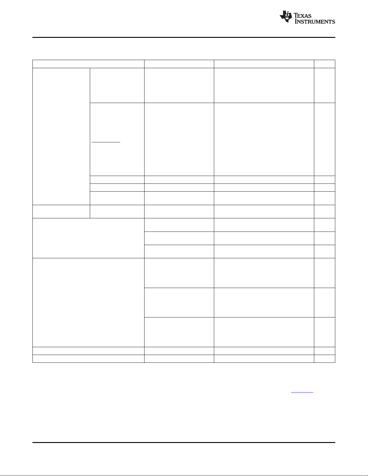
TMS320C6454
SPRS311F–APRIL 2006–REVISED SEPTEMBER 2010
www.ti.com
Electrical Characteristics Over Recommended Ranges of Supply Voltage and Operating Case
Temperature (Unless Otherwise Noted) (continued)
PARAMETER TEST CONDITIONS
AECLKOUT,
CLKR1/GP[0],
CLKX1/GP[3],
SYSCLK4/GP[1],
EMU[18:0], CLKR0,
CLKX0
EMIF pins (except
AECLKOUT), NMI,
TOUT0L, TINP0L,
TOUTP1L, TINP1L,
PCI_EN,
OL
Low-level output
current [DC]
I
EMAC-capable pins
(except RGMII pins), 4 mA
RESETSTAT,
McBSP-capable pins
(except CLKR1/GP[0],
CLKX1/GP[3], CLKR0,
CLKX0), GP[7:4], and
TDO
PCI-capable pins
(2)
RGMII pins 8 mA
DDR2 memory
controller pins
I
OZ
current [DC]
3.3-V pins VO= DV
or 0 V -20 20 uA
DD33
Off-state output
(5)
CVDD= 1.25 V,
CPU frequency = 1000 MHz
P
Core supply power
CDD
(6)
CVDD= 1.2 V,
CPU frequency = 850 MHz
CVDD= 1.2 V,
CPU frequency = 720 MHz
DV
= 3.3 V,
DD33
DV
= 1.8 V,
DD18
PLLV1 = PLLV2 = AV
AV
= 1.8 V,
DLL2
CPU frequency = 1000 MHz
DV
= 3.3 V,
DD33
DV
= 1.8 V,
P
C
C
I/O supply power
DDD
Input capacitance 10 pF
i
Output capacitance 10 pF
o
(6)
DD18
PLLV1 = PLLV2 = AV
AV
= 1.8 V,
DLL2
CPU frequency = 850 MHz
DV
= 3.3 V,
DD33
DV
= 1.8 V,
DD18
PLLV1 = PLLV2 = AV
AV
= 1.8 V,
DLL2
CPU frequency = 720 MHz
(5) IOZapplies to output-only pins, indicating off-state (hi-Z) output leakage current.
(6) Assumes the following conditions: 60% CPU utilization; DDR2 at 50% utilization (250 MHz), 50% writes, 32 bits, 50% bit switching; two
2-MHz McBSPs at 100% utilization, 50% switching; two 75-MHz Timers at 100% utilization; device configured for HPI32 mode with
pull-up resistors on HPI pins; room temperature (25°C). The actual current draw is highly application-dependent. For more details on
core and I/O activity, see the TMS320C6455/54 Power Consumption Summary application report (literature number SPRAAE8).
(1)
MIN TYP MAX UNIT
1.66 W
1.41 W
1.29 W
= 0.53 W
DLL1
= 0.53 W
DLL1
= 0.52 W
DLL1
8 mA
1.5 mA
-4 mA
96 Device Operating Conditions Copyright © 2006–2010,TexasInstruments Incorporated
Submit Documentation Feedback
Product Folder Link(s): TMS320C6454
Page 97
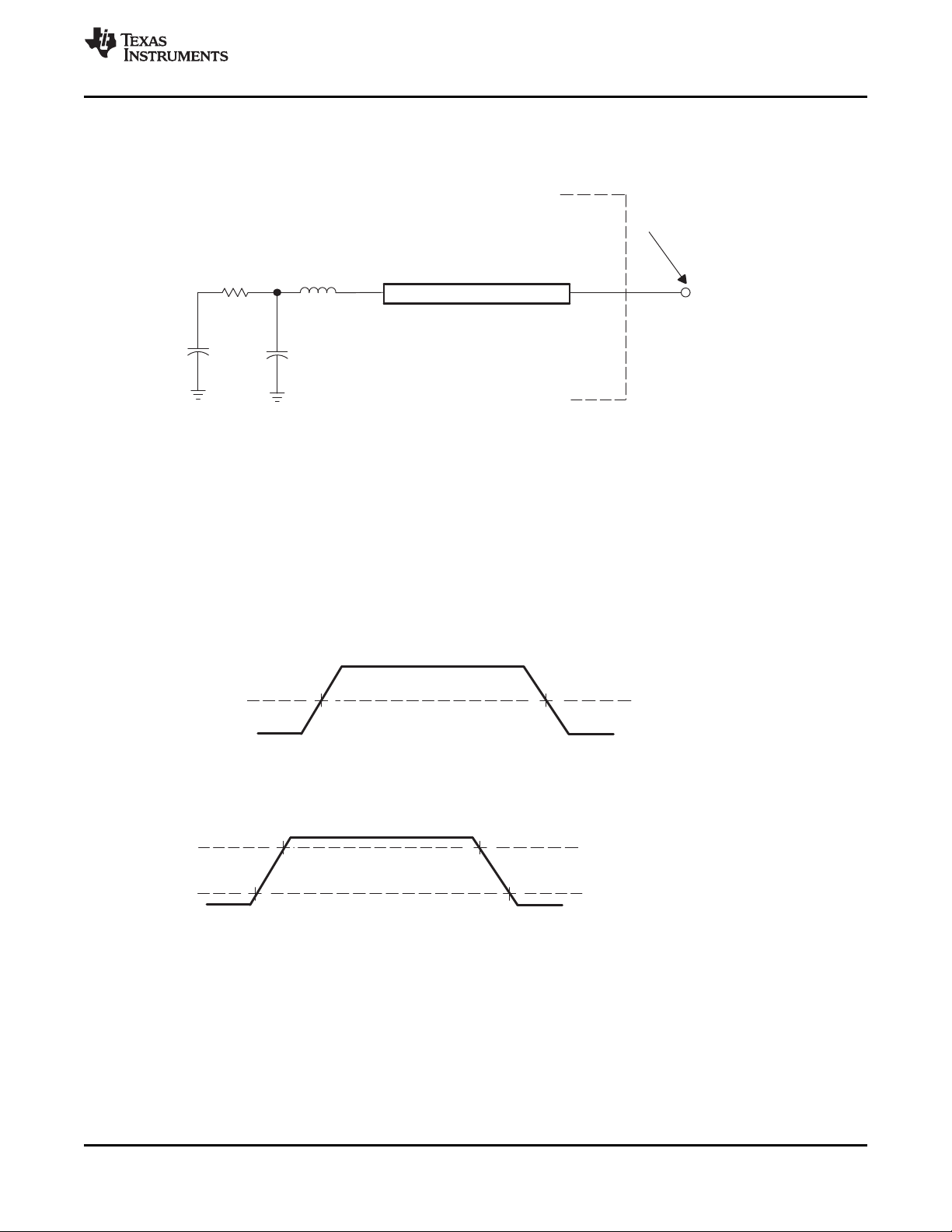
Transmission Line
4.0 pF 1.85 pF
Z0 = 50 Ω
(see Note)
Tester Pin Electronics
Data Sheet Timing Reference Point
Output
Under
Test
NOTE: The data sheet provides timing at the device pin. For output timing analysis, the tester pin electronics and its transmission line ef fects must
be taken into account. A transmission line with a delay of 2 ns can be used to produce the desired transmission line effect. The transmission
line is intended as a load only. It is not necessary to add or subtract the transmission line delay (2 ns) from the data sheet timings.
Input requirements in this data sheet are tested with an input slew rate of < 4 Volts per nanosecond (4 V/ns) at the device pin.
42 Ω 3.5 nH
Device Pin
(see Note)
V
ref
= 1.5 V
V
ref
= VIL MAX (or VOL MAX)
V
ref
= VIH MIN (or VOH MIN)
TMS320C6454
www.ti.com
SPRS311F–APRIL 2006–REVISED SEPTEMBER 2010
7 C64x+ Peripheral Information and Electrical Specifications
7.1 Parameter Information
Figure 7-1. Test Load Circuit for AC Timing Measurements
The load capacitance value stated is only for characterization and measurement of AC timing signals. This
load capacitance value does not indicate the maximum load the device is capable of driving.
7.1.1 3.3-V Signal Transition Levels
All input and output timing parameters are referenced to 1.5 V for both "0" and "1" logic levels.
Figure 7-2. Input and Output Voltage Reference Levels for AC Timing Measurements
All rise and fall transition timing parameters are referenced to VILMAX and VIHMIN for input clocks,
VOLMAX and VOHMIN for output clocks.
Figure 7-3. Rise and Fall Transition Time Voltage Reference Levels
7.1.2 3.3-V Signal Transition Rates
All timings are tested with an input edge rate of 4 volts per nanosecond (4 V/ns).
7.1.3 Timing Parameters and Board Routing Analysis
The timing parameter values specified in this data sheet do not include delays by board routings. As a
good board design practice, such delays must always be taken into account. Timing values may be
Copyright © 2006–2010, Texas Instruments Incorporated C64x+ Peripheral Information and Electrical Specifications 97
Submit Documentation Feedback
Product Folder Link(s): TMS320C6454
Page 98
1
2
3
4
5
6
7
8
10
11
AECLKOUT
(Output from DSP)
AECLKOUT
(Input to External Device)
Control Signals
(A)
(Output from DSP)
Control Signals
(Input to External Device)
Data Signals
(B)
(Output from External Device)
Data Signals
(B)
(Input to DSP)
9
TMS320C6454
SPRS311F–APRIL 2006–REVISED SEPTEMBER 2010
adjusted by increasing/decreasing such delays. TI recommends utilizing the available I/O buffer
information specification (IBIS) models to analyze the timing characteristics correctly. To properly use IBIS
models to attain accurate timing analysis for a given system, see the Using IBIS Models for Timing
Analysis application report (literature number SPRA839). If needed, external logic hardware such as
buffers may be used to compensate any timing differences.
For inputs, timing is most impacted by the round-trip propagation delay from the DSP to the external
device and from the external device to the DSP. This round-trip delay tends to negatively impact the input
setup time margin, but also tends to improve the input hold time margins (see Table 7-1 and Figure 7-4).
Figure 7-4 represents a general transfer between the DSP and an external device. The figure also
represents board route delays and how they are perceived by the DSP and the external device.
Table 7-1. Board-Level Timing Example
NO. DESCRIPTION
1 Clock route delay
2 Minimum DSP hold time
3 Minimum DSP setup time
4 External device hold time requirement
5 External device setup time requirement
6 Control signal route delay
7 External device hold time
8 External device access time
9 DSP hold time requirement
10 DSP setup time requirement
11 Data route delay
www.ti.com
(see Figure 7-4)
A. Control signals include data for Writes.
B. Data signals are generated during Reads from an external device.
7.2 Recommended Clock and Control Signal Transition Behavior
All clocks and control signals must transition between VIHand VIL(or between VILand VIH) in a monotonic
manner.
98 C64x+ Peripheral Information and Electrical Specifications Copyright © 2006–2010, Texas Instruments Incorporated
Figure 7-4. Board-Level Input/Output Timings
Submit Documentation Feedback
Product Folder Link(s): TMS320C6454
Page 99
DV
DD33
CV
DD12
All other
power supplies
1
2
TMS320C6454
www.ti.com
SPRS311F–APRIL 2006–REVISED SEPTEMBER 2010
7.3 Power Supplies
7.3.1 Power-Supply Sequencing
TI recommends the power-supply sequence shown in Figure 7-5. After the DV
remaining power supplies can be powered up at the same time as CVDDas long as their supply voltage
never exceeds the CVDDvoltage during powerup. Some TI power-supply devices include features that
facilitate power sequencing; for example, Auto-Track or Slow-Start/Enable features. For more information,
visit www.ti.com/dsppower.
Figure 7-5. Power-Supply Sequence
Table 7-2. Timing Requirements for Power-Supply Sequence
NO. UNIT
1 t
su(DVDD33-CVDD12)
2 t
su(CVDD12-ALLSUP)
Setup time, DV
Setup time, CV
supply stable before CV
DD33
supply stable before all other supplies stable 0 200 ms
DD12
supply stable 0.5 200 ms
DD12
supply is stable, the
DD33
-720
-850
A-1000/-1000
MIN MAX
7.3.2 Power-Supply Decoupling
In order to properly decouple the supply planes from system noise, place as many capacitors (caps) as
possible close to the DSP. These caps need to be close to the DSP, no more than 1.25 cm maximum
distance to be effective. Physically smaller caps are better, such as 0402, but need to be evaluated from a
yield/manufacturing point-of-view. Parasitic inductance limits the effectiveness of the decoupling
capacitors, therefore physically smaller capacitors should be used while maintaining the largest available
capacitance value. As with the selection of any component, verification of capacitor availability over the
product's production lifetime should be considered.
7.3.3 Power-Down Operation
One of the power goals for the C6454 device is to reduce power dissipation due to unused peripherals.
There are different ways to power down peripherals on the C6454 device.
Some peripherals can be statically powered down at device reset through the device configuration pins
(see Section 3.1, Device Configuration at Device Reset). Once in a static power-down state, the peripheral
is held in reset and its clock is turned off. Peripherals cannot be enabled once they are in a static
power-down state. To take a peripheral out of the static power-down state, a device reset must be
executed with a different configuration pin setting.
After device reset, all peripherals on the C6454 device are in a disabled state and must be enabled by
software before being used. It is possible to enable only the peripherals needed by the application while
keeping the rest disabled. Note that peripherals in a disabled state are held in reset with their clocks
gated. For more information on how to enable peripherals, see Section 3.3, Peripheral Selection After
Device Reset.
Peripherals used for booting, like I2C and HPI, are automatically enabled after device reset. It is not
possible to disable these peripherals after the boot process is complete.
Copyright © 2006–2010, Texas Instruments Incorporated C64x+ Peripheral Information and Electrical Specifications 99
Submit Documentation Feedback
Product Folder Link(s): TMS320C6454
Page 100

TMS320C6454
SPRS311F–APRIL 2006–REVISED SEPTEMBER 2010
The C64x+ Megamodule also allows for software-driven power-down management for all of the C64x+
megamodule components through its Power-Down Controller (PDC). The CPU can power-down part or
the entire C64x+ megamodule through the power-down controller based on its own execution thread or in
response to an external stimulus from a host or global controller. More information on the power-down
features of the C64x+ Megamodule can be found in the TMS320C64x+ Megamodule Reference Guide
(literature number SPRU871).
7.3.4 Preserving Boundary-Scan Functionality on RGMII and DDR2 Memory Pins
When the RGMII mode of the EMAC is not used, the DV
pins can be connected directly to ground (VSS) to save power. However, this will prevent boundary-scan
from functioning on the RGMII pins of the EMAC. To preserve boundary-scan functionality on the RGMII
pins, DV
• DV
• V
REFHSTL
DV
, V
DD15
DD15
REFHSTL
and DV
- connect to a voltage of DV
supply using two 1-kΩ resistors to form a resistor divider circuit.
DD18
, RSV14, and RSV13 should be connected as follows:
DD15MON
- connect these pins to the 1.8-V I/O supply (DV
/2. The DV
DD18
• RSV13 - connect this pin to ground (VSS) via a 200-Ω resistor.
• RSV14 - connect this pin to the 1.8-V I/O supply (DV
Similarly, when the DDR2 Memory Controller is not used, the V
connected directly to ground (VSS) to save power. However, this will prevent boundary-scan from
functioning on the DDR2 Memory Controller pins. To preserve boundary-scan functionality on the DDR2
Memory Controller pins, V
• V
REFSSTL
DV
- connect to a voltage of DV
supply using two 1-kΩ resistors to form a resistor divider circuit.
DD18
REFSSTL
, RSV11, and RSV12 should be connected as follows:
/2. The DV
DD18
• RSV11 - connect this pin to ground (VSS) via a 200-Ω resistor.
• RSV12 - connect this pin to the 1.8-V I/O supply (DV
, DV
DD15
/2 voltage can be generated directly from the
DD18
DD18
/2 voltage can be generated directly from the
DD18
DD18
DD15MON
) via a 200-Ω resistor.
REFSSTL
) via a 200-Ω resistor.
, V
DD18
REFHSTL
, RSV13, and RSV14
).
, RSV11, and RSV12 pins can be
www.ti.com
100 C64x+ Peripheral Information and Electrical Specifications Copyright © 2006–2010, Texas Instruments Incorporated
Submit Documentation Feedback
Product Folder Link(s): TMS320C6454
 Loading...