

Page 1

TMS320C6452 DSP
Host Port Interface (HPI)
User's Guide
Literature Number: SPRUF87A
October 2007 – Revised May 2008
Page 2

2 SPRUF87A – October 2007 – Revised May 2008
Submit Documentation Feedback
Page 3

Contents
Preface ........................................................................................................................................ 6
1 Introduction ......................................................................................................................... 9
1.1 Purpose of the Peripheral ................................................................................................ 9
1.2 Features .................................................................................................................... 9
1.3 Functional Block Diagram .............................................................................................. 10
1.4 Industry Standard(s) Compliance Statement ........................................................................ 11
1.5 Terminology Used in This Document ................................................................................. 11
2 Peripheral Architecture ....................................................................................................... 12
2.1 Clock Control ............................................................................................................. 12
2.2 Memory Map ............................................................................................................ 12
2.3 Signal Descriptions ...................................................................................................... 12
2.4 Pin Multiplexing .......................................................................................................... 12
2.5 Protocol Description ..................................................................................................... 12
2.6 Endianness Considerations ............................................................................................ 12
2.7 Architecture and Operation ............................................................................................. 14
2.8 Reset Considerations ................................................................................................... 31
2.9 Initialization ............................................................................................................... 32
2.10 Interrupt Support ......................................................................................................... 32
2.11 EDMA Event Support ................................................................................................... 34
2.12 Power Management ..................................................................................................... 34
2.13 Emulation Considerations .............................................................................................. 34
3 Registers ........................................................................................................................... 35
3.1 Peripheral Identification Register (PID) ............................................................................... 35
3.2 Power and Emulation Management Register (PWREMU_MGMT) ............................................... 36
3.3 Host Port Interface Control Register (HPIC) ......................................................................... 37
3.4 Host Port Interface Write Address Register (HPIAW) .............................................................. 39
3.5 Host Port Interface Read Address Register (HPIAR) ............................................................... 40
SPRUF87A – October 2007 – Revised May 2008 Table of Contents 3
Submit Documentation Feedback
Page 4

www.ti.com
List of Figures
1 HPI Block Diagram ......................................................................................................... 11
2 Example of Host-Processor Signal Connections ....................................................................... 15
3 HPI Strobe and Select Logic .............................................................................................. 16
4 16-bit Multiplexed-Mode Host Read Cycle .............................................................................. 19
5 16-bit Multiplexed-Mode Host Write Cycle .............................................................................. 20
6 Multiplexed-Mode Single-Halfword HPIC Cycle (Read or Write) .................................................... 21
7 HRDY Behavior During an HPIC or HPIA Read Cycle in the 16-bit Multiplexed Mode ........................... 22
8 HRDY Behavior During a Data Read Operation in the 16-bit Multiplexed Mode (Case 1: HPIA Write
Cycle Followed by Nonauto-increment HPID Read Cycle) ........................................................... 22
9 HRDY Behavior During a Data Read Operation in the 16-bit Multiplexed Mode (Case 2: HPIA Write
Cycle Followed by Auto-increment HPID Read Cycles) .............................................................. 23
10 HRDY Behavior During an HPIC Write Cycle in the 16-bit Multiplexed Mode ..................................... 23
11 HRDY Behavior During a Data Write Operation in the 16-bit Multiplexed Mode (Case 1:
No Auto-incrementing) ..................................................................................................... 24
12 HRDY Behavior During a Data Write Operation in the 16-bit Multiplexed Mode (Case 2:
Auto-incrementing Selected, FIFO Empty Before Write) .............................................................. 24
13 HRDY Behavior During a Data Write Operation in the 16-bit Multiplexed Mode (Case 3:
Auto-incrementing Selected, FIFO Not Empty Before Write) ......................................................... 24
14 HRDY Behavior During an HPIC or HPIA Read Cycle in the 32-Bit Multiplexed Mode .......................... 25
15 HRDY Behavior During a Data Read Operation in the 16-Bit Multiplexed Mode (Case 1: HPIA Write
Cycle Followed by Non-auto-increment HPID Read Cycle) .......................................................... 25
16 HRDY Behavior During a Data Read Operation in the 32-Bit Multiplexed Mode (Case 2: HPIA Write
Cycle Followed by Auto-increment HPID Read Cycles) .............................................................. 26
17 HRDY Behavior During an HPIC Write Cycle in the 32-Bit Multiplexed Mode ..................................... 26
18 HRDY Behavior During a Data Write Operation in the 32-Bit Multiplexed Mode (Case 1: No
Auto-incrementing) ......................................................................................................... 27
19 HRDY Behavior During a Data Write Operation in the 32-Bit Multiplexed Mode (Case 2:
Auto-incrementing Selected, FIFO Empty Before Write) .............................................................. 27
20 HRDY Behavior During a Data Write Operation in the 32-Bit Multiplexed Mode (Case 3:
Auto-incrementing Selected, FIFO Not Empty Before Write) ......................................................... 28
21 FIFOs in the HPI ........................................................................................................... 29
22 Host-to-CPU Interrupt State Diagram.................................................................................... 32
23 CPU-to-Host Interrupt State Diagram.................................................................................... 33
24 Peripheral Identification Register (PID) .................................................................................. 35
25 Power and Emulation Management Register (PWREMU_MGMT) .................................................. 36
26 Host Port Interface Control Register (HPIC) – Owner (Host) Access Permissions................................ 37
27 Host Port Interface Control Register (HPIC)–Non-owner (DSP) Access Permissions ............................ 37
28 Host Port Interface Write Address Register (HPIAW) ................................................................. 39
29 Host Port Interface Read Address Register (HPIAR) ................................................................. 40
List of Figures4 SPRUF87A – October 2007 – Revised May 2008
Submit Documentation Feedback
Page 5

www.ti.com
List of Tables
1 HPI Pins ..................................................................................................................... 13
2 Options for Connecting Host and HPI Data Strobe Pins .............................................................. 17
3 Access Types Selectable With the HCNTL Signals ................................................................... 17
4 Cycle Types Selectable With the HCNTL and HR/ W Signals ........................................................ 18
5 HPI Registers Relative to Base Address 0200 0030h ................................................................. 35
6 Peripheral Identification Register (PID) Field Descriptions ........................................................... 35
7 Power and Emulation Management Register (PWREMU_MGMT) Field Descriptions ............................ 36
8 Host Port Interface Control Register (HPIC) Field Descriptions ..................................................... 38
9 Host Port Interface Write Address Register (HPIAW) Field Descriptions ........................................... 39
10 Host Port Interface Read Address Register (HPIAR) Field Descriptions ........................................... 40
SPRUF87A – October 2007 – Revised May 2008 List of Tables 5
Submit Documentation Feedback
Page 6

About This Manual
Notational Conventions
Preface
SPRUF87A – October 2007 – Revised May 2008
Read This First
This document describes the features and operation of the host port interface (HPI) in the TMS320C6452
Digital Signal Processor (DSP).
This document uses the following conventions.
• Hexadecimal numbers are shown with the suffix h. For example, the following number is 40
hexadecimal (decimal 64): 40h.
• Registers in this document are shown in figures and described in tables.
– Each register figure shows a rectangle divided into fields that represent the fields of the register.
Each field is labeled with its bit name, its beginning and ending bit numbers above, and its
read/write properties below. A legend explains the notation used for the properties.
– Reserved bits in a register figure designate a bit that is used for future device expansion.
Note: Acronyms 3PSW, CPSW, CPSW_3G, and 3pGSw are interchangeable and all refer to the 3
port gigabit switch.
TMS320C6452 DSP
Related Documents From Texas Instruments
The following documents describe the TMS320C6452 Digital Signal Processor (DSP). Copies of these
documents are available on the Internet at www.ti.com . Tip: Enter the literature number in the search box
provided at www.ti.com .
Data Manual—
SPRS371 — TMS320C6452 Digital Signal Processor Data Manual describes the signals, specifications
and electrical characteristics of the device.
CPU—
SPRU732 — TMS320C64x/C64x+ DSP CPU and Instruction Set Reference Guide describes the CPU
architecture, pipeline, instruction set, and interrupts for the TMS320C64x and TMS320C64x+ digital
signal processors (DSPs) of the TMS320C6000 DSP family. The C64x/C64x+ DSP generation
comprises fixed-point devices in the C6000 DSP platform. The C64x+ DSP is an enhancement of
the C64x DSP with added functionality and an expanded instruction set.
Reference Guides—
SPRUF85 — C6452 DSP DDR2 Memory Controller User's Guide describes the DDR2 memory
controller in the TMS320C6452 Digital Signal Processor (DSP). The DDR2/mDDR memory
controller is used to interface with JESD79D-2A standard compliant DDR2 SDRAM devices and
standard Mobile DDR SDRAM devices.
6 Preface SPRUF87A – October 2007 – Revised May 2008
Submit Documentation Feedback
Page 7

www.ti.com
TMS320C6452 DSP
SPRUF86 — C6452 Peripheral Component Interconnect (PCI) User's Guide describes the peripheral
component interconnect (PCI) port in the TMS320C6452 Digital Signal Processor (DSP). The PCI
port supports connection of the C642x DSP to a PCI host via the integrated PCI master/slave bus
interface. The PCI port interfaces to the DSP via the enhanced DMA (EDMA) controller. This
architecture allows for both PCI master and slave transactions, while keeping the EDMA channel
resources available for other applications.
SPRUF87 — C6452 DSP Host Port Interface (UHPI) User's Guide describes the host port interface
(HPI) in the TMS320C6452 Digital Signal Processor (DSP). The HPI is a parallel port through which
a host processor can directly access the CPU memory space. The host device functions as a
master to the interface, which increases ease of access. The host and CPU can exchange
information via internal or external memory. The host also has direct access to memory-mapped
peripherals. Connectivity to the CPU memory space is provided through the enhanced direct
memory access (EDMA) controller.
SPRUF89 — C6452 DSP VLYNQ Port User's Guide describes the VLYNQ port in the TMS320C6452
Digital Signal Processor (DSP). The VLYNQ port is a high-speed point-to-point serial interface for
connecting to host processors and other VLYNQ compatible devices. It is a full-duplex serial bus
where transmit and receive operations occur separately and simultaneously without interference.
SPRUF90 — C6452 DSP 64-Bit Timer User's Guide describes the operation of the 64-bit timer in the
C6452 Digital Signal Processor (DSP). The timer can be configured as a general-purpose 64-bit
timer, dual general-purpose 32-bit timers, or a watchdog timer.
SPRUF91 — C6452 DSP Multichannel Audio Serial Port (McASP) User's Guide describes the
multichannel audio serial port (McASP) in the C6452 Digital Signal Processor (DSP). The McASP
functions as a general-purpose audio serial port optimized for the needs of multichannel audio
applications. The McASP is useful for time-division multiplexed (TDM) stream, Inter-Integrated
Sound (I2S) protocols, and intercomponent digital audio interface transmission (DIT).
SPRUF92 — C6452 DSP Serial Port Interface (SPI) User's Guide discusses the Serial Port Interface
(SPI) in the C6452 Digital Signal Processor (DSP). This reference guide provides the specifications
for a 16-bit configurable, synchronous serial peripheral interface. The SPI is a programmable-length
shift register, used for high speed communication between external peripherals or other DSPs.
SPRUF93 — C6452 DSP Universal Asynchronous Receiver/Transmitter (UART) User's Guide
describes the universal asynchronous receiver/transmitter (UART) peripheral in the C6452 Digital
Signal Processor (DSP). The UART peripheral performs serial-to-parallel conversion on data
received from a peripheral device, and parallel-to-serial conversion on data received from the CPU.
SPRUF94 — C6452 DSP Inter-Integrated Circuit (I2C) Module User's Guide describes the
inter-integrated circuit (I2C) peripheral in the C6452 Digital Signal Processor (DSP). The I2C
peripheral provides an interface between the DSP and other devices compliant with the I2C-bus
specification and connected by way of an I2C-bus. External components attached to this 2-wire
serial bus can transmit and receive up to 8-bit wide data to and from the DSP through the I2C
peripheral. This document assumes the reader is familiar with the I2C-bus specification.
SPRUF95 — C6452 DSP General-Purpose Input/Output (GPIO) User's Guide describes the
general-purpose input/output (GPIO) peripheral in the C6452 Digital Signal Processor (DSP). The
GPIO peripheral provides dedicated general-purpose pins that can be configured as either inputs or
outputs. When configured as an input, you can detect the state of the input by reading the state of
an internal register. When configured as an output, you can write to an internal register to control
the state driven on the output pin.
SPRUF96 — C6452 DSP Telecom Serial Interface Port (TSIP) User's Guide is a multi-link serial
interface consisting of a maximum of two transmit data signals (or links), two receive data signals
(or links), two frame sync input signals, and two serial clock inputs. Internally the TSIP offers single
channel of timeslot data management and single DMA capability that allow individual timeslots to
be selectively processed.
SPRUF87A – October 2007 – Revised May 2008 Read This First 7
Submit Documentation Feedback
Page 8

TMS320C6452 DSP
SPRUF97 — TMS320C6452 DSP 3 Port Switch (3PSW) Ethernet Subsystem User's Guide describes
www.ti.com
the operation of the 3 port switch (3PSW) ethernet subsystem in the TMS320C6452 Digital Signal
Processor (DSP). The 3 port switch gigabit ethernet subsystem provides ethernet packet
communication and can be configured as an ethernet switch. It provides the serial gigabit media
independent interface (SGMII), the management data input output (MDIO) for physical layer device
(PHY) management.
Read This First8 SPRUF87A – October 2007 – Revised May 2008
Submit Documentation Feedback
Page 9

1 Introduction
The host port interface (HPI) provides a parallel port interface through which an external host processor
can directly access the TMS320C6452 processor's resources (configuration and program/data memories).
The external host device is asynchronous to the CPU clock and functions as a master to the HPI interface.
The HPI enables a host device and the C6452 processor to exchange information via internal or external
memory. Dedicated address (HPIA) and data (HPID) registers within the HPI provide the data path
between the external host interface and the processor resources. An HPI control register (HPIC) is
available to the host and the CPU for various configuration and interrupt functions.
1.1 Purpose of the Peripheral
The HPI enables an external host processor (host) to directly access program/data memory on the
processor using a parallel interface. The primary purpose is to provide a mechanism to move data to and
from the processor. In addition to data transfer, the host can also use the HPI to bootload the processor
by downloading program and data information to the processor's memory after power-up.
User's Guide
SPRUF87A – October 2007 – Revised May 2008
Host Port Interface (HPI)
1.2 Features
The HPI supports the following features:
• Multiplexed address/data
• Dual 16-bit halfword cycle access (internal data word is 32-bits wide)
• 32-bit-wide host data bus interface
• Internal data bursting using 8-word read and write, first-in first-out (FIFO) buffers
• HPI control register (HPIC) accessible by both the DSP CPU and the external host
• HPI address register (HPIA) accessible by both the DSP CPU and the external host
• Separate HPI address registers for read (HPIAR) and write (HPIAW) with configurable option for
operating as a single HPI address register
• HPI data register (HPID)/FIFOs providing data-path between external host interface and CPU
resources
• Multiple strobes and control signals to allow flexible host connection
• Asynchronous HRDY output to allow the HPI to insert wait states to the host
• Software control of data prefetching to the HPID/FIFOs
• Processor-to-Host interrupt output signal controlled by HPIC accesses
• Host-to-Processor interrupt controlled by HPIC accesses
• Memory-mapped peripheral identification register (PID)
• Bus holders on host data and address buses (these are actually external to HPI module)
SPRUF87A – October 2007 – Revised May 2008 Host Port Interface (HPI) 9
Submit Documentation Feedback
Page 10

Introduction
1.3 Functional Block Diagram
Figure 1 is a high-level block diagram showing how the HPI connects a host (left side of figure) and the
processor internal memory (right side of figure). Host activity is asynchronous to the internal processor
clock that drives the HPI. The host functions as a master to the HPI. When HPI resources are temporarily
busy or unavailable, the HPI communicates this to the host by de-asserting the HPI ready ( HRDY) output
signal.
The HPI uses multiplexed operation, meaning the data bus carries both address and data. When the host
drives an address on the bus, the address is stored in the address register (HPIA) in the HPI, so that the
bus can then be used for data.
The HPI supports two interface modes: HPI16 and HPI32 mode. DSP selects either HPI16 or HPI32 mode
with the help of HPI_WIDTH device configuration pin at reset.
-16-bit multiplexed mode (HPI16): The HPI is called HPI16 when operating as a 16-bit wide host port. This
mode is selected if the HPI_WIDTH configuration pin of the DSP is sampled low at reset. In this mode, a
16-bit data bus (HD[15:0]) carries both addresses and data. HPI16 combines successive 16-bit transfers
to provide 32-bit data to the CPU. The halfword identification line (HHWIL) input is used on the HPI16 to
identify the first or second half word of a word transfer.
-32-bit multiplexed mode (HPI32): HPI operates in this mode as a 32-bit wide host port. This mode is
selected if the HPI_WIDTH configuration pin of the DSP is sampled high at reset. In this mode, a 32-bit
data bus (HD[31:0]) carries both addresses and data. HHWIL is not applicable for HPI32 mode.
The HPI contains two HPIAs (HPIAR and HPIAW), which can be used as separate address registers for
read accesses and write accesses(for details, see Section 2.7.1 ).
A control register (HPIC) is accessible by the CPU and the host. The CPU uses HPIC to send an interrupt
request to the host, to clear an interrupt request from the host, and to configure and monitor the HPI.
Data flow between the host and the HPI uses a temporary storage register, the 32-bit data register (HPID).
Data arriving from the host is held in HPID until the data can be stored elsewhere in the processor. Data
to be sent to the host is held in HPID until the HPI is ready to perform the transfer. When address
auto-incrementing is used, read and write FIFOs are used to store burst data. If auto-incrementing is not
used, the FIFO memory acts as a single register (only one location is used).
Note: To manage data transfers between HPID and the internal memory, the DSP contains dedicated HPI
DMA logic. The HPI DMA logic is not programmable. It automatically stores or fetches data using the
address provided by the host. The HPI DMA logic is independent of the EDMA3 controller included in the
DSP.
In the DSP system, master and slave peripherals communicate with each other via the Switched Central
Resource (SCR). By definition, master peripherals are capable of initiating read and write transfers in the
system and may not solely rely on the EDMA3 controller for their data transfers. Slave peripherals rely on
the EDMA3 controller to perform transfers. The HPI is a master peripheral; it uses its DMA logic to directly
communicate with the rest of the system via the SCR and does not rely on the EDMA3 controller for its
data transfers. Note that the HPI cannot access all DSP resources or peripherals; see the device-specific
data manual for a list of resources accessible through the HPI.
www.ti.com
Host Port Interface (HPI)10 SPRUF87A – October 2007 – Revised May 2008
Submit Documentation Feedback
Page 11
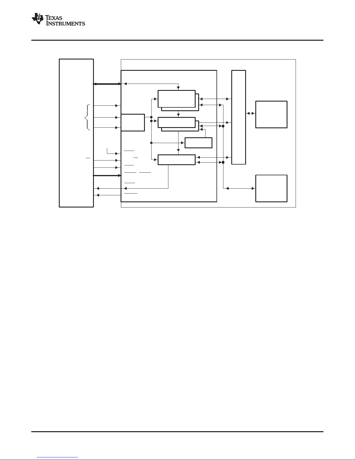
HPID
R/WFIFOs
HPIA
Increment
HPIC
Access
type
HD[15:0]
HDS1,HDS2
HR/W
HAS
HCNTL0
HCNTL1
HINT
HRDY
HPI
Host
Data
Address
orI/O
R/W
Data
strobes
IRQ
Ready
CPU
HCSChipselect
Processor
memory
HPIDMA
logic
Processor
HHWIL
high
Logic
www.ti.com
Introduction
Figure 1. HPI Block Diagram
1.4 Industry Standard(s) Compliance Statement
The HPI is not an industry standard interface that is developed and monitored by an international
organization. It is a generic parallel interface that can be configured to gluelessly interface, a variety of
parallel devices.
1.5 Terminology Used in This Document
The following is a brief explanation of some terms used in this document:
Term Meaning
CPU DSP CPU
host External host device
HPI DMA logic Logic used to communicate between the HPI and the DMA system that moves data to
processor the entire digital media system-on-chip
and from memory. This is independent of the EDMA system on the processor
SPRUF87A – October 2007 – Revised May 2008 Host Port Interface (HPI) 11
Submit Documentation Feedback
Page 12

Peripheral Architecture
2 Peripheral Architecture
2.1 Clock Control
The HPI clock is derived from SYSCLK2, which is the PLL1 clock divided by 6. For detailed information on
the PLLs and clock distribution on the processor, see the Subsystem User's Guide.
2.2 Memory Map
The HPI can be used by the host to access the following processor resources:
• HPI configuration registers
• Most on-chip device memory, peripherals, and memory-mapped registers (see Section 4, System
Interconnect, in the device-specific data manual for more detailed information)
• DDR2 Memory Controller configuration register file and memory address ranges
• Power and Sleep Controller (PSC) registers
• PLL1 and PLL2 registers
Consult the device-specific data manual for the memory address ranges of the above resources.
2.3 Signal Descriptions
Table 1 shows the a description of the HPI signals.
www.ti.com
2.4 Pin Multiplexing
2.5 Protocol Description
2.6 Endianness Considerations
On the C6452 extensive pin multiplexing is used to accommodate the largest number of peripheral
functions in the smallest possible package. Pin multiplexing is controlled using a combination of hardware
configuration at device reset and software programmable register settings. UHPI pins are multiplexed with
PCI pins' functionality. The configuration pin UHPIEN is to be set to 1 to enable UHPI. Refer to the
device-specific data manual to determine how pin multiplexing affects the HPI.
The HPI does not conform to any industry standard protocol. Details on the nature of address, data and
control transactions are found in the following sections.
The HPI operation is independent of the C6452 endianness mode; therefore, there are no endianness
considerations for the HPI.
Host Port Interface (HPI)12 SPRUF87A – October 2007 – Revised May 2008
Submit Documentation Feedback
Page 13

www.ti.com
Peripheral Architecture
Table 1. HPI Pins
Pin Type Host Connection Function
HCNTL[1:0] I Address or control pins HPI access control inputs. The HPI latches the logic levels of these pins
HCS I Chip select pin HPI chip select. HCS must be low for the HPI to be selected by the host.
HR/ W I R/W strobe pin HPI read/write. On the falling edge of internal HSTRB, HR/ W indicates
HHWIL I Address or control pins Halfword identification line. The host uses HHWIL to identify the first
HAS I None Address strobe. Connect to logic high.
HINT O/Z Interrupt pin Host Interrupt. The CPU can interrupt the host processor by writing a 1
HDS1 and I Read strobe and write HPI data strobe pins. These pins are used for strobing data in and out of
HDS2 strobe pins or any data the HPI (for data strobing details, see Section 2.7.4 ). The direction of the
strobe pin data transfer depends on the logic level of the HR/ W signal. The HDS
HD[31:0] I/O/Z Data bus HPI data bus. The HPI data bus carries the address and data to/from the
HD[15:0] HPI. HD[31:0] applies to HPI32 and HD[15:0] applies to HPI16.
HRDY O/Z Asynchronous ready pin HPI-ready signal. When the HPI drives HRDY low, the host has
HINT O/Z Interrupt pin The DSP can interrupt the host processor by writing a 1 to the HINT bit of
on the falling edge of internal HSTRB (for details about internal HSTRB,
see Section 2.7.4 ). The four binary states of these pins determine the
access type of the current transfer (HPIC, HPIA, HPID with and without
auto-incrementing).
HCS can be kept low between accesses. HCS normally precedes an
active HDS (data strobe) signal, but can be connected to an HDS pin for
simultaneous select and strobe activity.
whether the current access is to be a read or write operation. Driving
HR/ W high indicates the transfer is a read from the HPI, while driving
HR/ W low indicates a write to the HPI.
and second halfwords of the host cycle. HHWIL must be driven low for the
first halfword and high for the second halfword.
to the HINT bit of HPIC. Before subsequent HINT interrupts can occur,
the host must acknowledge interrupts by writing a 1 to the HINT bit. This
pin is active-low (that is, when an interrupt is asserted from the host, the
state of this signal is low) and inverted from the HINT bit value in HPIC.
signals are also used to latch control information on the falling edge.
During an HPID write access, data is latched into the HPID register on the
rising edge of HDS. During read operations, these pins act as
output-enable pins of the host data bus.
permission to complete the current host cycle. When the HPI drives
HRDY high, the HPI is not ready for the current host cycle to complete.
HPIC. Before subsequent HINT interrupts can occur, the host must clear
previous interrupts by writing a 1 to the HINT bit. This pin is active-low
and inverted from the HINT bit value in HPIC.
SPRUF87A – October 2007 – Revised May 2008 Host Port Interface (HPI) 13
Submit Documentation Feedback
Page 14

Peripheral Architecture
2.7 Architecture and Operation
2.7.1 Using the Address Registers
The HPI contains two 32-bit address registers: one for read operations (HPIAR) and one for write
operations (HPIAW). These roles are unchanging from the viewpoint of the HPI logic. The HPI DMA logic
gets the address from HPIAR when reading from processor resources (see Section 2.2 ) and gets the
address from HPIAW when writing to processor resources (see Section 2.2 ).
However, unlike the HPI logic, the host can choose how to interact with the two HPI address registers.
Using the DUALHPIA bit in the HPI control register (HPIC), the host determines whether HPIAR and
HPIAW act as a single 32-bit register (single-HPIA mode) or as two independent 32-bit registers
(dual-HPIA mode).
Note: The addresses loaded into the HPI address registers must be word addresses, and must be
2.7.1.1 Single-HPIA Mode
When DUALHPIA = 0 in HPIC, HPIAR and HPIAW become a single HPI address register (HPIA) from the
perspective of the host. In this mode:
• A host HPIA write cycle (HCNTL[1:0] = 10b, HR/ W = 0) updates HPIAR and HPIAW with the same
value.
• Both HPI address registers are incremented during auto-increment read/write cycles
(HCNTL[1:0] = 01b).
• An HPIA read cycle (HCNTL[1:0] = 10b, HR/ W = 1) returns the content of HPIAR, which should be
identical to the content of HPIAW.
To maintain consistency between the contents of HPIAR and HPIAW, the host should always reinitialize
the HPI address registers after changing the state of the DUALHPIA bit. In addition, when DUALHPIA = 0,
the host must always reinitialize the HPI address registers when it changes the data direction (from an
HPID read cycle to an HPID write cycle, or conversely). Otherwise, the memory location accessed by the
HPI DMA logic might not be the location intended by the host.
www.ti.com
32-bit word aligned (with the least-significant two bits equal to zero), for use in addressing
memory space within the C6452. For example, to access L2 SRAM at 0x00A0_0000, HPIA
should be loaded with 0x0028_0000 (0x00A0_0000 divided by 4).
2.7.1.2 Dual-HPIA Mode
When DUALHPIA = 1 in HPIC, HPIAR and HPIAW are two independent HPI address registers from the
perspective of the host. In this mode:
• A host HPIA access (HCNTL[1:0] = 10b) reads/updates either HPIAR or HPIAW, depending on the
value of the HPIA read/write select (HPIASEL) bit in HPIC. This bit is programmed by the host. While
HPIASEL = 1, only HPIAR is read or updated by the host. While HPIASEL = 0, only HPIAW is read or
updated by the host. The HPIASEL bit is only meaningful in the dual-HPIA mode.
Note: The HPIASEL bit does not affect the HPI DMA logic. Regardless of the value of HPIASEL,
the HPI DMA logic uses HPIAR when reading from memory and HPIAW when writing to
memory.
• A host HPID access with auto-incrementing (HCNTL[1:0] = 01b) causes only the relevant HPIA value
to be incremented to the next consecutive memory address. In an auto-increment read cycle, HPIAR is
incremented after it has been used to perform the current read from memory. In an auto-increment
write cycle, HPIAW is incremented after it has been used for the write operation.
Host Port Interface (HPI)14 SPRUF87A – October 2007 – Revised May 2008
Submit Documentation Feedback
Page 15

Host
Address
orI/O
Read/Write
Processor
HPI
Logichigh
2
Chipselect
Datastrobe1
Datastrobe
HAS
HCNTL[1:0]
HHWIL
HR/W
HCS
HDS1
HDS2
(A)
32
HD[15:0]
Data
Ready
HRDY
Interrupt HINT
www.ti.com
2.7.2 Host-HPI Signal Connections
Figure 2 shows an example of a signal connection between the HPI and a host.
Peripheral Architecture
Figure 2. Example of Host-Processor Signal Connections
A Data strobing options are given in Section 2.7.4
2.7.3 HPI Configuration and Data Flow
The host accomplishes a multiplexed access in the following manner:
1. The host writes to the HPI control register (HPIC) to properly configure the HPI. Typically, this means
programming the halfword order bit (HWOB) and the HPIA-related bits (DUALHPIA and HPIASEL).
This step is normally performed once before the initial data access.
2. The host writes the desired internal processor memory address to an address register (HPIAR and/or
HPIAW). For an introduction to the two HPI address registers and the two ways the host can interact
with them, see Section 2.7.1 .
3. The host reads from or writes to the data register (HPID). Data transfers between HPID and the
Each step of the access uses the same bus. Therefore, the host must drive the appropriate levels on the
internal memory of the processor are handled by the HPI DMA logic and are transparent to the CPU.
HCNTL1 and HCNTL0 signals to indicate which register is to be accessed. The host must also drive the
appropriate level on the HR/ W signal to indicate the data direction (read or write) and must drive other
control signals as appropriate. When HPI resources are temporarily busy or unavailable, the HPI can
communicate this to the host by de-asserting the HPI-ready ( HRDY) output signal.
When performing an access, the HPI first latches the levels on HCNTL[1:0], HR/ W, and other control
signals. This latching can occur on the falling edge of the internal strobe signal (for details, see
Section 2.7.4 ). After the control information is latched, the HPI initiates an access based on the control
signals.
SPRUF87A – October 2007 – Revised May 2008 Host Port Interface (HPI) 15
Submit Documentation Feedback
Page 16

HDS1
HDS2
HCS
HRDY
Internal
HSTRB
Internal
HRDY
Peripheral Architecture
If the host wants to read data from processor resources (see Section 2.2 ), the HPI DMA logic reads the
resource address from HPIAR and retrieves the data from the addressed memory location. When the data
has been placed in HPID, the HPI drives the data onto its HD bus. The HRDY signal informs the host
whether the data on the HD bus is valid ( HRDY low) or not valid yet ( HRDY high). When the data is valid,
the host should latch the data and drive the connected data strobe ( HDS1 or HDS2) inactive, which, in
turn, will cause the internal strobe (internal HSTRB) signal to transition from low to high.
If the host wants to write data to processor resources (see Section 2.2 ), the operation is similar. After the
host determines that the HPI is ready to latch the data ( HRDY is low), it must cause internal HSTRB to
transition from low to high, which causes the data to be latched into HPID. Once the data is in HPID, the
HPI DMA logic reads the memory address from HPIAW and transfers the data from HPID to the
addressed memory location.
2.7.4 HDS2, HDS1, and HCS: Data Strobing and Chip Selection
As shown in Figure 3 , the strobing logic is a function of three key inputs: the chip select pin ( HCS) and two
data strobe signals ( HDS1 and HDS2). The internal strobe signal, which is referred to as internal HSTRB
throughout this document, functions as the actual strobe signal inside the HPI. HCS must be low (HPI
selected) during strobe activity on the HDS pins. If HCS remains high (HPI not selected), activity on the
HDS pins is ignored.
Figure 3. HPI Strobe and Select Logic
www.ti.com
Strobe connections between the host and the HPI depend in part on the number and types of strobe pins
available on the host. Table 2 describes some options for connecting to the HDS pins.
Notice in Figure 3 that HRDY is also gated by HCS. If HCS goes high (HPI not selected), HRDY goes low,
regardless of whether the current internal transfer is completed in the processor.
Note: The HCS input and one HDS strobe input can be tied together and driven with a single
strobe signal from the host. This technique selects the HPI and provides the strobe,
simultaneously. When using this method, be aware that HRDY is gated by HCS as
previously described.
It is not recommended to tie both HDS1 and HDS2 to static logic levels and use HCS as a
strobe.
Host Port Interface (HPI)16 SPRUF87A – October 2007 – Revised May 2008
Submit Documentation Feedback
Page 17

www.ti.com
Table 2. Options for Connecting Host and HPI Data Strobe Pins
Available Host Data Strobe Pins Connections to HPI Data Strobe Pins
Host has separate read and write strobe Connect one strobe pin to HDS1 and the other to HDS2
pins, both active-low provide a R/ W line, take care to satisfy HR/ W timings as stated in the device data
Host has separate read and write strobe Connect one strobe pin to HDS1 and the other to HDS2
pins, both active-high provide a R/ W line, take care to satisfy HR/ W timings as stated in the device data
Host has one active-low strobe pin Connect the strobe pin to HDS1 or HDS2, and connect the other pin to logic-level 1.
Host has one active-high strobe pin Connect the strobe pin to HDS1 or HDS2, and connect the other strobe pin to
(1)
The HR/ W signal could be driven by a host address line in this case.
manual. This could possibly be done using a host address line.
manual. This could possibly be done using a host address line.
logic-level 0.
2.7.5 HCNTL[1:0] and HR/ W: Indicating the Cycle Type
The cycle type consists of:
• The access type that the host selects by driving the appropriate levels on the HCNTL[1:0] pins of the
HPI. Table 3 describes the four available access types.
• The transfer direction that the host selects with the HR/ W pin. The host must drive the HR/ W signal
high (read) or low (write).
A summary of cycle types is in Table 4 . The HPI samples the HCNTL levels at the falling edge of the
internal strobe signal HSTRB.
Peripheral Architecture
(1)
. Since such a host might not
(1)
. Since such a host might not
Table 3. Access Types Selectable With the HCNTL Signals
HCNTL1
(1)
Note that the encoding of HCNTL0 and HCNTL1 for the different types of HPI accesses varies on many TI DSPs; therefore, you
should use caution to ensure that the correct encoding of these inputs is used for your device. The encoding of these signals as
described in this document applies only to the C6452.
(1)
0 0 HPIC access. The host requests to access the HPI control register (HPIC).
0 1 HPID access with auto-incrementing. The host requests to access the HPI data
1 0 HPIA access. The host requests to access the appropriate HPI address register (HPIAR
1 1 HPID access without auto-incrementing. The host requests to access the HPI data
HCNTL0
(1)
Access Type
register (HPID) and to have the appropriate HPI address register (HPIAR and/or HPIAW)
automatically incremented by 1 after the access.
and/or HPIAW).
register (HPID) but requests no automatic post-increment of the HPI address register.
SPRUF87A – October 2007 – Revised May 2008 Host Port Interface (HPI) 17
Submit Documentation Feedback
Page 18

Peripheral Architecture
Table 4. Cycle Types Selectable With the HCNTL and HR/ W Signals
HCNTL1
(1)
(1)
HCNTL0
0 0 0 HPIC write cycle
0 0 1 HPIC read cycle
0 1 0 HPID write cycle with auto-incrementing
0 1 1 HPID read cycle with auto-incrementing
1 0 0 HPIA write cycle
1 0 1 HPIA read cycle
1 1 0 HPID write cycle without auto-incrementing
1 1 1 HPID read cycle without auto-incrementing
Note that the encoding of HCNTL0 and HCNTL1 for the different types of HPI accesses varies on many TI DSPs; therefore, you
should use caution to ensure that the correct encoding of these inputs is used for your device. The encoding of these signals as
described in this document applies only to the C6452.
(1)
HR/ W Cycle Type
2.7.6 HHWIL: Identifying the First and Second Halfwords in Multiplexed Mode Transfers
Each host cycle consists of two consecutive halfword transfers. For each transfer, the host must specify
the cycle type with HCNTL[1:0] and HR/ W, and the host must use HHWIL to indicate whether the first or
second halfword is being transferred. For HPID and HPIA accesses, HHWIL must always be driven low for
the first halfword transfer and high for the second halfword transfer. Results are undefined if the sequence
is broken. For examples of using HHWIL, see Section 2.7.7 .
When the host sends the two halfwords of a 32-bit word in this manner, the host can send the
most-significant and the least-significant halfwords of the word in either order (most-significant halfword
first or most-significant halfword second). However, the host must inform the HPI of the selected order
before beginning the host cycle. This is done by programming the halfword order (HWOB) bit in HPIC.
Although HWOB is written at bit 0 in HPIC, its current value is readable at both bit 0 and bit 8
(HWOBSTAT). Thus, the host can determine the current halfword order configuration by checking the
least-significant bit of either half of HPIC.
There is one case when the HPI does not require a dual halfword access with HHWIL low for the first
halfword and HHWIL high for the second halfword. This is the case when accessing the HPIC register.
When accessing HPIC, the state of HHWIL is ignored and the same 16-bit HPIC register is accessed
regardless of whether the host performs a single or dual access. For an example timing diagram of this
case, see Section 2.7.8 .
www.ti.com
18 Host Port Interface (HPI) SPRUF87A – October 2007 – Revised May 2008
Submit Documentation Feedback
Page 19
Data 2Data 1
HCS
HSTRB
HR/W
HCNTL[1:0]
HD[15:0]
HRDY
HHWIL
Internal
HPI latches
control information
Host latches
data
HPI latches
control information
Host latches
data
www.ti.com
2.7.7 Performing a Multiplexed Access
Figure 2 shows an example of signal connections for multiplexed transfers. Figure 4 and Figure 5 show
typical HPI signal activity when performing a read and write transfer, respectively. In these cases, the
falling edge of internal HSTRB is used to latch the HCNTL[1:0], HR/ W, and HHWIL states into the HPI.
Internal HSTRB is derived from HCS, HDS1, and HDS2 as described in Section 2.7.4 .
Peripheral Architecture
Figure 4. 16-bit Multiplexed-Mode Host Read Cycle
SPRUF87A – October 2007 – Revised May 2008 Host Port Interface (HPI) 19
Submit Documentation Feedback
NOTE: Depending on the type of write operation (HPID without auto-incrementing, HPIA, HPIC, or HPID with
auto-incrementing) and the state of the FIFO, transitions on HRDY may or may not occur. For more information, see
Section 2.7.9 .
Page 20

HCS
HSTRB
HRDY
HR/W
HCNTL[1:0]
HHWIL
Data1 Data2
HD[15:0]
Internal
HPIlatches
controlinformation
HPIlatches
data
HPIlatches
controlinformation
HPIlatches
data
Peripheral Architecture
www.ti.com
Figure 5. 16-bit Multiplexed-Mode Host Write Cycle
NOTE: Depending on the type of write operation (HPID without auto-incrementing, HPIA, HPIC, or HPID with
auto-incrementing) and the state of the FIFO, transitions on HRDY may or may not occur. For more information, see
Section 2.7.9 .
20 Host Port Interface (HPI) SPRUF87A – October 2007 – Revised May 2008
Submit Documentation Feedback
Page 21

Data 1
HCS
HSTRB
HR/W
HCNTL[1:0]
HD[15:0]
HRDY
HHWIL
Internal
Valid
00
Valid
www.ti.com
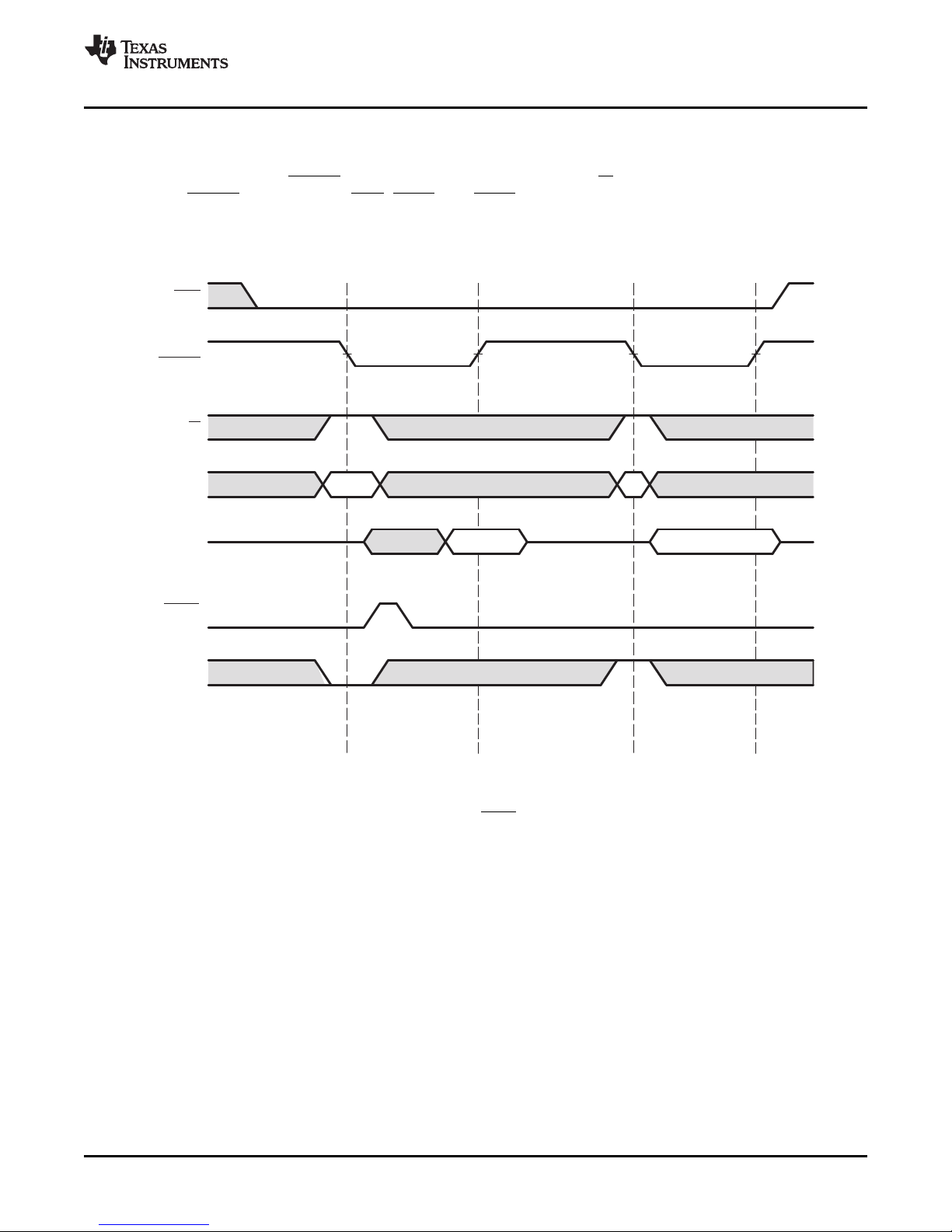
2.7.8 Single-Halfword HPIC Cycle in 16-bit Multiplexed Mode
Figure 6 shows the special case (see Section 2.7.6 ) when the host performs a single-halfword cycle to
access the HPIC. The state of HHWIL is ignored and if a dual-halfword access is performed, then the
same HPIC register is accessed twice.
Figure 6. Multiplexed-Mode Single-Halfword HPIC Cycle (Read or Write)
Peripheral Architecture
2.7.9 Hardware Handshaking Using the HPI-Ready ( HRDY) Signal
The HPI uses its ready signal, HRDY, to tell the host whether it is ready to complete an access. During a
read cycle, the HPI is ready (drives HRDY high) when it has data available for the host. During a write
cycle, the HPI is ready (drives HRDY high) when it is ready to latch data from the host. If the HPI is not
ready, it can drive HRDY low to insert wait states. These wait states indicate to the host that read data is
not yet valid (read cycle) or that the HPI is not ready to latch write data (write cycle). The number of wait
states that must be inserted by the HPI is dependent upon the state of the resource that is being
accessed.
When the HPI is not ready to complete the current cycle ( HRDY low), the host can begin a new host cycle
by forcing the HPI to latch new control information. However, once the cycle has been initiated, the host
must wait until HRDY goes high before causing a rising edge on the internal strobe signal (internal
HSTRB) to complete the cycle. If internal HSTRB goes high when the HPI is not ready, the cycle will be
terminated with invalid data being returned (read cycle) or written (write cycle).
One reason the HPI may drive HRDY low is a not-ready condition in one of its first-in, first-out buffers
(FIFOs). For example, any HPID access that occurs while the write FIFO is full or the read FIFO is empty
may result in some number of wait states being inserted by the HPI. The FIFOs are explained in
Section 2.7.10 .
The following sections describe the behavior of HRDY during HPI register accesses. In all cases, the chip
select signal, HCS, must be asserted for HRDY to go low.
SPRUF87A – October 2007 – Revised May 2008 Host Port Interface (HPI) 21
Submit Documentation Feedback
Page 22

1sthalfword
00or10 00or10
2ndhalfword
Internal
HD[15:0]
HRDY
HHWIL
HR/W
HCNTL[1:0]
HCS
HSTRB
HCS
HAS
HCNTL[1:0 ]
HR/W
HHWIL
Internal
HSTRB
HD[15:0 ]
HRDY
1sthalfword 2ndhalfword 1sthalfword
2ndhalfword
11 111010
Peripheral Architecture
2.7.9.1 HRDY Behavior During 16-bit Multiplexed-Mode Read Operations
Figure 7 shows an HPIC (HCNTL[1:0] = 00b) or HPIA (HCNTL[1:0] = 10b) read cycle. Neither an HPIC
read cycle nor an HPIA read cycle causes HRDY to go low. For this type of access, the state of HHWIL is
ignored, so if a dual halfword access is performed, the same register will be accessed twice.
Figure 7. HRDY Behavior During an HPIC or HPIA Read Cycle in the 16-bit Multiplexed Mode
Figure 8 includes an HPID read cycle without auto-incrementing. The host writes the memory address
during the HPIA (HCNTL[1:0] = 10b) write cycle, and the host reads the data during the HPID
(HCNTL[1:0] = 11b) read cycle. HRDY goes low for each HPIA halfword access, but HRDY goes low for
only the first halfword access in each HPID read cycle.
Figure 8. HRDY Behavior During a Data Read Operation in the 16-bit Multiplexed Mode
(Case 1: HPIA Write Cycle Followed by Nonauto-increment HPID Read Cycle)
www.ti.com
Figure 9 includes an auto-increment HPID read cycle. The host writes the memory address while
asserting HCNTL[1:0] = 10b and reads the data while asserting HCNTL[1:0] = 01b. During the first HPID
read cycle, HRDY goes low for only the first halfword access, and subsequent HPID read cycles do not
cause HRDY to go low.
Host Port Interface (HPI)22 SPRUF87A – October 2007 – Revised May 2008
Submit Documentation Feedback
Page 23

HCS
HAS
Internal
HRDY
HD[15:0]
HR/W
HCNTL[1:0]
HHWIL
10 10 01 01 01
1st halfword2ndhalfword1sthalfword2ndhalfword1sthalfword
HSTRB
1sthalfword 2ndhalfword
00
00
Internal
HD[15:0]
HRDY
HHWIL
HR/W
HCNTL[1:0]
HAS
HCS
HSTRB
www.ti.com
Figure 9. HRDY Behavior During a Data Read Operation in the 16-bit Multiplexed Mode
(Case 2: HPIA Write Cycle Followed by Auto-increment HPID Read Cycles)
2.7.9.2 HRDY Behavior During 16-bit Multiplexed-Mode Write Operations
Figure 10 shows an HPIC (HCNTL[1:0] = 00b) write cycle operation. An HPIC write cycle does not cause
HRDY to go low and the state of HHWIL is ignored. Firmware is not required to perform a dual access to
access HPIC.
Figure 10. HRDY Behavior During an HPIC Write Cycle in the 16-bit Multiplexed Mode
Peripheral Architecture
Figure 11 includes a HPID write cycle without auto-incrementing. The host writes the memory address
while HCNTL[1:0] = 10b and writes the data while HCNTL[1:0] = 11b. During the HPID write cycle, HRDY
goes low only for the second halfword access.
SPRUF87A – October 2007 – Revised May 2008 Host Port Interface (HPI) 23
Submit Documentation Feedback
Page 24

1sthalfword 2ndhalfword2ndhalfword1sthalfword
Internal
HSTRB
HD[15:0]
HRDY
HHWIL
HR/W
HCNTL[1:0]
HAS
HCS
10
11
10
11
10 10 01 01 01
1sthalfword2ndhalfword1sthalfword2ndhalfword1sthalfword
Internal
HSTRB
HD[15:0]
HRDY
HHWIL
HR/W
HCNTL[1:0]
HAS
HCS
10 10 01 01 01
1sthalfword2ndhalfword1sthalfword2ndhalfword1sthalfword
Internal
HSTRB
HD[15:0]
HRDY
HHWIL
HR/W
HCNTL[1:0]
HAS
HCS
Peripheral Architecture
www.ti.com
Figure 11. HRDY Behavior During a Data Write Operation in the 16-bit Multiplexed Mode
(Case 1: No Auto-incrementing)
Figure 12 shows auto-increment HPID write cycles when the write FIFO is empty prior to the HPIA write.
The host writes the memory address while HCNTL[1:0] = 10b and writes the data while HCNTL[1:0] = 01b.
HRDY does not go low during any of the HPID write cycles until the FIFO is full.
Figure 12. HRDY Behavior During a Data Write Operation in the 16-bit Multiplexed Mode
(Case 2: Auto-incrementing Selected, FIFO Empty Before Write)
Figure 13 shows a case similar to that of Figure 12 . However, in the case of Figure 13 , the write FIFO is
not empty when the HPIA access is made. HRDY goes low twice for the first halfword access of the HPIA
write cycle. The first HRDY low period is due to the nonempty FIFO. The data currently in the FIFO must
first be written to the memory. This results in HRDY going low immediately after the falling edge of the
data strobe ( HSTRB). The second and third HRDY low periods occur for the writes to the HPIA. HRDY
remains high for the HPID accesses.
Figure 13. HRDY Behavior During a Data Write Operation in the 16-bit Multiplexed Mode
(Case 3: Auto-incrementing Selected, FIFO Not Empty Before Write)
24 Host Port Interface (HPI) SPRUF87A – October 2007 – Revised May 2008
Submit Documentation Feedback
Page 25

HCS
HCNTL[1:0]
HR/W
Internal
HSTRB
HD[31:0]
HRDY
00or10
HCS
HCNTL[1:0]
HR/W
Internal
HSTRB
HD[31:0]
HRDY
10 11
HPIA Write HPIDRead
www.ti.com
2.7.9.3 HRDY Behavior During 32-bit Multiplexed-Mode Read Operations
Figure 14 shows an HPIC (HCNTL[1:0] = 00b) read or an HPIA (HCNTL[1:0] = 01b) read access for 32-bit
multiplexed HPI operation. Note that neither an HPIC nor an HPIA read access causes HRDY to become
active.
Figure 14. HRDY Behavior During an HPIC or HPIA Read Cycle in the 32-Bit Multiplexed Mode
Peripheral Architecture
Figure 15 shows an HPIA (HCNTL[1:0] = 10b) write access followed by an HPID (HCNTL[1:0] = 11b) read
access for 32-bit multiplexed HPI operation.
Figure 15. HRDY Behavior During a Data Read Operation in the 16-Bit Multiplexed Mode
(Case 1: HPIA Write Cycle Followed by Non-auto-increment HPID Read Cycle)
Figure 16 shows an HPIA (HCNTL[1:0] = 10b) write access followed by several auto-increment HPID
(HCNTL[1:0] = 01b) read accesses. Note that HRDY is active for the HPIA access. HRDY is also active
for the first HPID read access, but not for subsequent read accesses.
SPRUF87A – October 2007 – Revised May 2008 Host Port Interface (HPI) 25
Submit Documentation Feedback
Page 26

HCS
(A)
HCNTL[1:0]
HR/W
Internal
HSTRB
HD[31:0]
HRDY
10
01
HPIA Write HPID+Reads
01 01
HCS
HCNTL[1:0]
HR/W
Internal
HSTRB
HD[31:0]
HRDY
00
Peripheral Architecture
Figure 16. HRDY Behavior During a Data Read Operation in the 32-Bit Multiplexed Mode
(Case 2: HPIA Write Cycle Followed by Auto-increment HPID Read Cycles)
2.7.9.4 HRDY Behavior During 32-bit Multiplexed-Mode Write Operations
Figure 17 shows an HPIC (HCNTL[1:0] = 00b) write access for 32-bit multiplexed HPI operation. Note that
an HPIC write access does not cause HRDY to become active.
www.ti.com
Figure 17. HRDY Behavior During an HPIC Write Cycle in the 32-Bit Multiplexed Mode
Figure 18 shows an HPIA (HCNTL[1:0] = 10b) write access followed by an HPID (HCNTL[1:0] = 11b) write
access for 32-bit multiplexed HPI operation.
Host Port Interface (HPI)26 SPRUF87A – October 2007 – Revised May 2008
Submit Documentation Feedback
Page 27

HCS
HCNTL[1:0]
HR/W
Internal
HSTRB
HD[31:0]
HRDY
10 11
HPIA Write HPIDWrite
HCS
(A)
HCNTL[1:0]
HR/W
Internal
HSTRB
HD[31:0]
HRDY
10
01
HPIA Write HPID+Writes
01 01
www.ti.com
Peripheral Architecture
Figure 18. HRDY Behavior During a Data Write Operation in the 32-Bit Multiplexed Mode
(Case 1: No Auto-incrementing)
Figure 19 shows an HPIA (HCNTL[1:0] = 10b) write access followed by several auto-incrementing HPID
(HCNTL[1:0] = 01b) write accesses when the write FIFO is empty. Note that HRDY is active during the
HPIA access but not active during any of the HPID accesses.
Figure 19. HRDY Behavior During a Data Write Operation in the 32-Bit Multiplexed Mode
(Case 2: Auto-incrementing Selected, FIFO Empty Before Write)
Figure 20 shows an HPIA (HCNTL[1:0] = 10b) write access when the write FIFO is not empty, followed by
several auto-incrementing HPID (HCNTL[1:0] = 01b) write accesses. Note that HRDY is active twice for
the HPIA access. This occurs because the FIFO is not empty and the data in the FIFO must first be
written to memory. This results in an HRDY assertion immediately after the falling edge of the data-strobe
(HSTRB). When a write request to memory has been made that will empty the internal FIFO, the HPIA
write operation can complete with the rising edge of HSTRB. The second HRDY assertion is for the write
to the HPIA register. HRDY is not active for the HPID accesses.
SPRUF87A – October 2007 – Revised May 2008 Host Port Interface (HPI) 27
Submit Documentation Feedback
Page 28

HCS
(A)
HCNTL[1:0]
HR/W
Internal
HSTRB
HD[31:0]
HRDY
10
01
HPIA Write HPID+Writes
01 01
Peripheral Architecture
Figure 20. HRDY Behavior During a Data Write Operation in the 32-Bit Multiplexed Mode
2.7.10 FIFOs and Bursting
The HPI data register (HPID) is a port through which the host accesses two first-in, first-out buffers
(FIFOs). As shown in Figure 21 , a read FIFO supports host read cycles, and a write FIFO supports host
write cycles. Both read and write FIFOs are 8-words deep (each word is 32 bits). If the host is performing
multiple reads or writes to consecutive memory addresses (auto-increment HPID cycles), the FIFOs are
used for bursting. The HPI DMA logic reads or writes a burst of four words at a time when accessing one
of the FIFOs.
Bursting is essentially invisible to the host because the host interface signaling is not affected. Its benefit
to the host is that the HRDY signal is de-asserted less often when there are multiple reads or writes to
consecutive addresses.
www.ti.com
(Case 3: Auto-incrementing Selected, FIFO Not Empty Before Write)
Host Port Interface (HPI)28 SPRUF87A – October 2007 – Revised May 2008
Submit Documentation Feedback
Page 29

Write FIFO
control logic
Host write
pointer
HPI DMA
read pointer
Write FIFO
Host
writes
Read FIFO
reads
Host
control logic
Read FIFO
Host read
pointer
HPI DMA
write pointer
HPI
DMA
logic
Processor
memory
Burst
writes
reads
Burst
www.ti.com
Peripheral Architecture
Figure 21. FIFOs in the HPI
2.7.10.1 Read Bursting
When the host writes to the read address register (HPIAR), the read FIFO is flushed. Any host read data
that was in the read FIFO is discarded (the read FIFO pointers are reset). If an HPI DMA write to the read
FIFO is in progress at the time of a flush request, the HPI allows this write to complete and then performs
the flush.
Read bursting can begin in one of two ways: the host initiates an HPID read cycle with auto-incrementing,
or the host initiates issues a FETCH command (writes 1 to the FETCH bit in HPIC).
If the host initiates an HPID read cycle with auto-incrementing, the HPI DMA logic performs two 4-word
burst operations to fill the read FIFO. The host is initially held off by the de-assertion of the HRDY signal
until data is available to be read from the read FIFO. Once data is available in the read FIFO, the host can
read data from the read FIFO by performing subsequent reads of HPID with auto-incrementing. Once the
initial read has been performed, the HPI DMA logic continues to perform 4-word burst operations to
consecutive memory addresses every time there are four empty word locations in the read FIFO. The HPI
DMA logic continues to prefetch data to keep the read FIFO full, until the occurrence of an event that
causes a read FIFO flush (see Section 2.7.10.3 ).
As mentioned, the second way that read bursting may begin is with a FETCH command. The host should
always precede the FETCH command with the initialization of the HPIAR register or a nonauto-increment
access, so that the read FIFO is flushed beforehand. When the host initiates a FETCH command, the HPI
DMA logic begins to prefetch data to keep the read FIFO full, as described in the previous paragraph. The
FETCH bit in HPIC does not actually store the value that is written to it; rather, the decoding of a host
write of 1 to this bit is considered a FETCH command.
The FETCH command can be helpful if the host wants to minimize a stall condition on the interface. The
host can initiate prefetching by writing 1 to the FETCH bit and later perform a read. The host can make
use of the time it takes to load the read FIFO with read data, during which the HPI was not ready, by using
the CPU to service other tasks.
SPRUF87A – October 2007 – Revised May 2008 Host Port Interface (HPI) 29
Submit Documentation Feedback
Page 30

Peripheral Architecture
2.7.10.2 Write Bursting
www.ti.com
Both types of continuous or burst reads described in the previous paragraphs begin with a write to the HPI
address register, which causes a read FIFO flush. This is the typical way of initiating read cycles, because
the initial read address needs to be specified.
Note: An HPID read cycle without auto-incrementing does not initiate any prefetching activity.
Instead, it causes the read FIFO to be flushed and causes the HPI DMA logic to perform a
single-word read from the processor memory. As soon as the host activates a read cycle
without auto-incrementing, prefetching activity ceases until the occurrence of a FETCH
command or an auto-increment read cycle.
A write to the write address register (HPIAW) causes the write FIFO to be flushed. This means that any
write data in the write FIFO is forced to its destination in the processor memory (the HPI DMA logic
performs burst operations until the write FIFO is empty). When the FIFO has been flushed, the only action
that will cause the HPI DMA logic to perform burst writes is a host write to HPID with auto-incrementing.
The initial host-write data is stored in the write FIFO. An HPI DMA write is not requested until there are
four words in the write FIFO. As soon as four words have been written to the FIFO via HPID write cycles
with auto-incrementing, the HPI DMA logic performs a 4-word burst operation to the processor memory.
The burst operations continue as long as there are at least four words in the FIFO. If the FIFO becomes
full (eight words are waiting in the FIFO), the HPI holds off the host by de-asserting HRDY until at least
one empty word location is available in the FIFO.
Because excessive time might pass between consecutive burst operations, the HPI has a time-out
counter. If there are fewer than four words in the write FIFO and the time-out counter expires, the HPI
DMA logic empties the FIFO immediately by performing a 2-word or 3-word burst, or a single-word write,
as necessary. Every time new data is written to the write FIFO, the time-out counter is automatically reset
to begin its count again. The time-out period is programmable and is configured by writing to the TIMOUT
bits in the HPI configuration register (HPI_CTL). Note that you should only modify the TIMOUT bits once
during device initialization. When modifying the TIMOUT bits, you must ensure that the HPI FIFOs are
empty and there are no on-going HPI transactions.
In an actual system environment, the TIMOUT value should generally be set considerably larger than the
typical time expected for the host to fill half of the FIFO. If the TIMOUT value is set less than this, HPI
throughput performance can be significantly reduced due to excessive FIFO flushing that will result in
more frequent not-ready conditions on the host interface, and decrease the overall effectiveness of the
FIFO.
A practical worst-case value would be to set the timeout to the maximum latency that can be tolerated
after the last word is written from the host before the HPI initiates a transfer to memory. Note that
calculation of the value for worst-case latency should take into account the time required to perform the
data transfer to memory, so that the overall system latency requirements are met.
Note: An HPID write cycle without auto-incrementing does not initiate any bursting activity. Instead,
it causes the write FIFO to be flushed and causes the HPI DMA logic to perform a
single-word write to the processor memory. As soon as the host activates a write cycle
without auto-incrementing, bursting activity ceases until the occurrence of an auto-increment
write cycle. A nonauto-increment write cycle always should be preceded by the initialization
of HPIAW or by another nonauto-increment access, so that the write FIFO is flushed
beforehand.
2.7.10.3 FIFO Flush Conditions
When specific conditions occur within the HPI, the read or write FIFO must be flushed to prevent the
reading of stale data from the FIFOs. When a read FIFO flush condition occurs, all current host accesses
and direct memory accesses (DMAs) to the read FIFO are allowed to complete. This includes DMAs that
have been requested but not yet initiated. The read FIFO pointers are then reset, causing any read data to
be discarded.
30 Host Port Interface (HPI) SPRUF87A – October 2007 – Revised May 2008
Submit Documentation Feedback
Page 31

www.ti.com
Peripheral Architecture
Similarly, when a write FIFO flush condition occurs, all current host accesses and DMAs to the write FIFO
are allowed to complete. This includes DMAs that have been requested but not yet initiated. All posted
writes in the FIFO are then forced to completion with a final burst or single-word write, as necessary.
If the host initiates an HPID host cycle during a FIFO flush, the cycle is held off with the de-assertion of
HRDY until the flush is complete and the FIFO is ready to be accessed.
The following conditions cause the read and write FIFOs to be flushed:
• Read FIFO flush conditions:
– A value from the host is written to the read address register (HPIAR).
– The host performs an HPID read cycle without auto-incrementing.
• Write FIFO flush conditions:
– A value from the host is written to the write address register (HPIAW).
– The host performs an HPID write cycle without auto-incrementing.
– The write-burst time-out counter expires.
When operating with DUALHPIA = 0, any read or write flush condition causes both read and write FIFOs
to be flushed. In addition, the following scenarios cause both FIFOs to be flushed when DUALHPIA = 0:
• The host performs a write to the HPIA register.
• The host performs an HPID write cycle with auto-incrementing while the read FIFO is not empty (the
read FIFO still contains data from prefetching or an HPID read cycle with auto-incrementing).
• The host performs an HPID read cycle with auto-incrementing while the write FIFO is not empty (there
is still posted write data in the write FIFO).
This is useful in providing protection against reading stale data by reading a memory address when a
previous write cycle has not been completed at the same address. Similarly, this protects against
overwriting data at a memory address when a previous read cycle has not been completed at the same
address.
When operating with DUALHPIA = 1 (HPIAR and HPIAW are independent), there is no such protection.
However, when DUALHPIA = 1, data flow can occur in both directions without flushing both FIFOs
simultaneously, thereby improving HPI bandwidth.
2.7.10.4 FIFO Behavior When a Hardware Reset Occurs
A hardware reset (RESET pin driven low) causes the FIFOs to be reset. The FIFO pointers are cleared,
so that all data in the FIFOs are discarded. In addition, all associated FIFO logic is reset.
If a host cycle is active when a hardware or HPI software reset occurs, the HRDY signal is asserted
(driven low), allowing the host to complete the cycle. When the cycle is complete, HRDY is de-asserted
(driven high). Any access interrupted by a reset may result in corrupted read data or a lost write data (if
the write does not actually update the intended memory or register). Although data may be lost, the host
interface protocol is not violated. While either of reset condition is true, and the host is idle (internal
HSTRB is held high), the FIFOs are held in reset, and host transactions are held off with an inactive
HRDY signal.
2.8 Reset Considerations
The HPI has two reset sources: software reset and hardware reset.
2.8.1 Software Reset Considerations
The HPI is not affected by a software reset issued by the emulator.
2.8.2 Hardware Reset Considerations
When the entire processor is reset with the RESET pin:
• If the internal strobe signal, internal HSTRB, is high (host is inactive), HRDY is driven low and remains
low until the reset condition is over.
SPRUF87A – October 2007 – Revised May 2008 Host Port Interface (HPI) 31
Submit Documentation Feedback
Page 32

DSPINT=0
DSPINT=1
CPU writes 1
to DSPINT bit
Interrupt
pending
Host writes 0
to DSPINT bit
No interrupt/
interrupt
cleared
Host writes 0 or 1
to DSPINT bit
CPU writes 0
to DSPINT bit
CPU writes 0 or 1
to DSPINT bit
Host writes 1
to DSPINT bit
(interrupt generated
to CPU)
(A)
Peripheral Architecture
2.9 Initialization
2.10 Interrupt Support
www.ti.com
• If internal HSTRB is low (host cycle is active), HRDY is driven high, allowing the host to complete the
cycle. When internal HSTRB goes high (cycle is complete), HRDY is driven low and remains low until
the reset condition is over. If the active cycle was a write cycle, the memory or register may not have
been correctly updated. If the active cycle was a read cycle, the fetched value may not be valid.
• The HPI registers are reset to their default values (see Section 3 ).
• The read and write FIFOs and the associated FIFO logic are reset (this includes a flush of the FIFOs).
• Host-to-CPU and CPU-to-host interrupts are cleared.
The following steps are required to configure the HPI after a hardware reset:
1. Perform the necessary device pin multiplexing setup (see the device-specific data manual).
2. Choose how HPIAR and HPIAW will be controlled by configuring the DUALHPIA bit in HPIC.
3. Choose how halfword ordering will be handled by configuring the HWOB bit in HPIC.
4. Choose how the HPI will respond to emulation suspend events by configuring the FREE and SOFT
bits in PWREMU_MGMT.
5. Choose the desired initial addresses and write the addresses to HPIAW and HPIAR, appropriately.
The HPI is now ready to perform data transactions.
The host can interrupt the CPU via the DSPINT bit in HPIC, as described in Section 2.10.1 . The CPU can
send an interrupt to the host by using the HINT bit in HPIC, as described in Section 2.10.2 .
2.10.1 DSPINT Bit: Host-to-CPU Interrupts
The DSPINT bit in HPIC allows the host to send an interrupt request to the CPU. The use of the DSPINT
bit is summarized in Figure 22 .
Figure 22. Host-to-CPU Interrupt State Diagram
A When the DSPINT bit transitions from 0 to 1, an interrupt is generated to the CPU. No new interrupt can be generated
until the CPU has cleared the bit (DSPINT = 0).
To interrupt the CPU, the host must:
1. Drive both HCNTL1 and HCNTL0 low to request a write to HPIC.
32 Host Port Interface (HPI) SPRUF87A – October 2007 – Revised May 2008
Submit Documentation Feedback
Page 33

HINT bit=0
HINT signal
is high
is low
HINT signal
HINT bit=1
CPU writes 1
to HINT bit
Host writes 1
to HINT bit
Interrupt
active
CPU writes 0
to HINT bit
No interrupt/
interrupt
cleared
Host writes 0 or 1
to HINT bit
CPU writes 0 or 1
to HINT bit
Host writes 0
to HINT bit
www.ti.com
2. Write 1 to the DSPINT bit in HPIC.
When the host sets the DSPINT bit, the HPI generates an interrupt pulse to the CPU. If this maskable
interrupt is properly enabled in the CPU, the CPU executes the corresponding interrupt service routine
(ISR).
Before the host can use DSPINT to generate a subsequent interrupt to the CPU, the CPU must
acknowledge the current interrupt by writing a 1 to the DSPINT bit. When the CPU writes 1, DSPINT is
forced to 0. The host should verify that DSPINT = 0 before generating subsequent interrupts. While
DSPINT = 1, host writes to the DSPINT bit do not generate an interrupt pulse.
Writes of 0 have no effect. A hardware reset immediately clears DSPINT and thus clears an active
host-to-CPU interrupt.
Note: When the HPIC is owned by the processor (not the host), the host is allowed to write into the
interrupt fields in the HPIC register.
2.10.2 HINT Bit: CPU-to-Host Interrupts
The HINT bit in HPIC allows the CPU to send an interrupt request to the host. The use of the HINT bit is
summarized in Figure 23 .
Peripheral Architecture
Figure 23. CPU-to-Host Interrupt State Diagram
If the CPU writes 1 to the HINT bit of HPIC, the HPI drives the HINT signal low, indicating an interrupt
condition to the host. Before the CPU can use the HINT bit generate a subsequent interrupt to host, the
host must acknowledge the current interrupt by writing 1 to the HINT bit. When the host does this, the HPI
clears the HINT bit (HINT = 0), and this drives the HINT signal high. The CPU should read HPIC and
make sure HINT = 0 before generating subsequent interrupts.
Writes of 0 have no effect. A hardware reset immediately clears the HINT bit and thus clears an active
CPU-to-host interrupt.
SPRUF87A – October 2007 – Revised May 2008 Host Port Interface (HPI) 33
Submit Documentation Feedback
Note: When the HPIC is owned by the processor (not the host), the host is allowed to write into the
interrupt fields in the HPIC register.
Page 34

Peripheral Architecture
2.10.3 Interrupt Multiplexing
The HPI has a single interrupt source to the DSP CPU. This interrupt source is not multiplexed with any
other interrupt source on the CPU.
2.11 EDMA Event Support
The HPI does not provide synchronization events to the EDMA system. Memory accesses from the HPI
are handled automatically, independent of the EDMA controller. The HPI controller has its own dedicated
DMA and its operation and configuration are transparent.
2.12 Power Management
The HPI peripheral can be placed in reduced-power modes to conserve power during periods of low
activity. The power management of the HPI peripheral is controlled by the processor Power and Sleep
Controller (PSC). The PSC acts as a master controller for power management for all of the peripherals on
the device. For detailed information on power management procedures using the PSC, see the
Subsystem User's Guide.
2.13 Emulation Considerations
The FREE and SOFT bits in the power and emulation management register (PWREMU_MGMT)
determine the response of the HPI to an emulation suspend condition. If FREE = 1, the HPI is not
affected, and the SOFT bit has no effect. If FREE = 0 and SOFT = 0, the HPI is not affected. If FREE = 0
and SOFT = 1:
• The HPI DMA logic halts after the current host and HPI DMA operations are completed.
• The external host interface functions as normal throughout the emulation suspend condition. The host
may access the control register (HPIC). The host may also access the HPIA registers and may perform
data reads until the read FIFO is empty or data writes until the write FIFO is full. As in normal
operation, HRDY is driven low during a host cycle that cannot be completed due to the write FIFO
being full or the read FIFO being empty. If this occurs, HRDY continues to be driven low, holding off
the host, until the emulation suspend condition is over, and the FIFOs are serviced by the HPI DMA
logic, allowing the host cycle to complete.
• When the emulation suspend condition is over, the appropriate requests by the HPI DMA logic are
made to process any posted host writes in the write FIFO or to fill the read FIFO as necessary. HPI
operation then continues as normal.
www.ti.com
34 Host Port Interface (HPI) SPRUF87A – October 2007 – Revised May 2008
Submit Documentation Feedback
Page 35

www.ti.com
3 Registers
Table 5 lists the memory-mapped registers for the HPI. See the device-specific data manual for the
memory addresses of these registers.
Table 5. HPI Registers Relative to Base Address 0200 0030h
Offset Acronym Register Description Section
0h PID Peripheral Identification Register Section 3.1
4h PWREMU_MGMT Power and Emulation Management Register Section 3.2
30h HPIC Host Port Interface Control Register Section 3.3
34h HPIAW Host Port Interface Write Address Register Section 3.4
38h HPIAR Host Port Interface Read Address Register Section 3.5
3.1 Peripheral Identification Register (PID)
The peripheral identification register (PID) contains identification data (class, revision, and type) for the
peripheral. PID is shown in Figure 24 and described in Table 6 .
Registers
Figure 24. Peripheral Identification Register (PID)
31 24 23 16
Reserved TID
R-0 R-1
15 8 7 0
CID PREV
R-2h R-0
LEGEND: R = Read only; - n = value after reset
Table 6. Peripheral Identification Register (PID) Field Descriptions
Bit Field Value Description
31-24 Reserved 0 Reserved
23-16 TID 0-Fh Identifies type of peripheral.
1 HPI module
15-8 CID 0-Fh Identifies class of peripheral.
2h Host port.
7-0 PREV 0-Fh Identifies revision of peripheral.
2h Current revision of peripheral.
SPRUF87A – October 2007 – Revised May 2008 Host Port Interface (HPI) 35
Submit Documentation Feedback
Page 36

Registers
3.2 Power and Emulation Management Register (PWREMU_MGMT)
The power and emulation management register (PWREMU_MGMT) determines the emulation mode of
the HPI. PWREMU_MGMT is shown in Figure 25 and described in Table 7 .
Figure 25. Power and Emulation Management Register (PWREMU_MGMT)
31 16
Reserved
R-0
15 2 1 0
Reserved SOFT FREE
R-0 R/W-0 R/W-0
LEGEND: R/W = Read/Write; R = Read only; - n = value after reset
Table 7. Power and Emulation Management Register (PWREMU_MGMT) Field Descriptions
Bit Field Value Description
31-2 Reserved 0 Reserved
1 SOFT Determines emulation mode functionality of the HPI. When the FREE bit is cleared to 0, the SOFT bit
selects the HPI mode.
0 Upon emulation suspend, the HPI operation is not affected.
1 In response to an emulation suspend event, the HPI logic halts after the current HPI transaction is
completed.
0 FREE Free run emulation control. Determines emulation mode functionality of the HPI. When the FREE bit is
cleared to 0, the SOFT bit selects the HPI mode.
0 The SOFT bit selects the HPI mode.
1 The HPI runs free regardless of the SOFT bit.
www.ti.com
Host Port Interface (HPI)36 SPRUF87A – October 2007 – Revised May 2008
Submit Documentation Feedback
Page 37

www.ti.com
3.3 Host Port Interface Control Register (HPIC)
The host port interface control register (HPIC) stores configuration and control information for the HPI. As
shown in Figure 26 and Figure 27 and described in Table 8 , the owner (Host) and non-owner (DSP) do
not have the same access permissions. The owner (Host) of HPIC has full read/write access; the
non-owner (DSP) of HPIC has primarily read-only access, but the exceptions are:
• the non-owner (DSP) can write 1 to the HINT bit to generate an interrupt to the host.
• the non-owner (DSP) can write 1 to HPI_RST bit to cause an HPI software reset.
Figure 26. Host Port Interface Control Register (HPIC) – Owner (Host) Access Permissions
31 16
Reserved
R-0
15 12 11 10 9 8
Reserved HPIASEL Reserved DUALHPIA HWOBSTAT
R-0 R/W-0 R/W-0 R/W-0 R-0
7 6 5 4 3 2 1 0
HPI_RST Reserved FETCH Reserved HINT DSPINT HWOB
(1)
R/W-0 R/W-0 R-1 R/W1C-0 R/W-0 R/W-0
Registers
LEGEND: R/W = Read/Write; R = Read only; W1C = Write 1 to clear (writing 0 has no effect);; - n = value after reset
(1)
Default value after reset = 0, when HPI boot used. See Table 8 for details.
Figure 27. Host Port Interface Control Register (HPIC)–Non-owner (DSP) Access Permissions
31 16
Reserved
R-0
15 12 11 10 9 8
Reserved HPIASEL Reserved DUALHPIA HWOBSTAT
R-0 R-0 R-0 R-0 R-0
7 6 5 4 3 2 1 0
HPI_RST Reserved FETCH Reserved HINT DSPINT HWOB
(1)
LEGEND: R/W = Read/Write; R = Read only; W1C = Write 1 to clear (writing 0 has no effect);; - n = value after reset
(1)
Default value after reset = 0, when HPI boot used. See Table 8 for details.
R-0 R-0 R-1 R/W-0 R/W1C-0 R-0
SPRUF87A – October 2007 – Revised May 2008 Host Port Interface (HPI) 37
Submit Documentation Feedback
Page 38

Registers
Table 8. Host Port Interface Control Register (HPIC) Field Descriptions
Bit Field Value Description
31-12 Reserved 0 Reserved
11 HPIASEL HPI address register select bit. When DUALHPIA = 1, the HPIASEL bit is used to select the HPI
address register to be accessed.
0 Selects the HPI write address register (HPIAW).
1 Selects the HPI read address register (HPIAR).
10 Reserved 0 Reserved. Always write 0 to this bit.
9 DUALHPIA Dual HPIA mode configuration bit. The CPU can access both HPI address registers separately,
regardless of the DUALHPIA setting. (Regardless of this bit, dual HPIA mode is implied when the
CPU has ownership of the HPI address registers).
0 The two HPI address registers (HPIAW and HPIAR) operate as a single HPI address register in
terms of host accesses.
1 Dual HPIA mode operation is enabled.
8 HWOBSTAT HWOB status. The value of the HWOB bit is also stored in this bit position. A write to the HWOB bit
also updates HWOBSTAT.
0 HWOB bit is logic 0.
1 HWOB bit is logic 1.
7 HPI_RST HPI reset
0 Default value after reset, when HPI boot used
1 Default value after reset, when boot other than HPI is used. The DSP must clear this bit before
making any host access through HPI.
6-5 Reserved Reserved. Always write 0 to this bit.
4 FETCH Host data fetch request bit. Only the host may write to FETCH. When a host writes a 1 to FETCH, a
request is posted in the HPI to prefetch data into the read FIFO. Host and CPU reads of FETCH
return a 0.
3 Reserved 1 Reserved
2 HINT Processor-to-host interrupt. The CPU writes a 1 to HINT to generate a host interrupt. HINT has an
inverted logic level to the HINT pin. The host must write a 1 to HINT to clear the HINT pin; writing a
0 to HINT by the host or processor has no effect.
0 No effect.
1 A CPU write generates a host interrupt ( HINT signal goes low). A host write sets the HINT signal
high (clears the interrupt).
1 DSPINT Host-to-processor interrupt. The host writes a 1 to DSPINT to generate a processor interrupt;
writing a 0 to DSPINT by the host or processor has no effect.
0 No effect
1 A host write generates a processor interrupt. A DSP write clears the interrupt/bit.
0 HWOB Halfword ordering bit. HWOB affects both data and address transfers. HWOB must be initialized
before the first data or address register access.
0 First halfword is most significant.
1 First halfword is least significant.
www.ti.com
Host Port Interface (HPI)38 SPRUF87A – October 2007 – Revised May 2008
Submit Documentation Feedback
Page 39

www.ti.com
3.4 Host Port Interface Write Address Register (HPIAW)
The HPI contains two 32-bit address registers: one for read operations (HPIAR) and one for write
operations (HPIAW). The host port interface write address register (HPIAW) is shown in Figure 28 and
described in Table 9 . The HPI can be configured such that HPIAR and HPIAW act as a single 32-bit HPIA
(single-HPIA mode) or as two separate 32-bit HPIAs (dual-HPIA mode) from the perspective of the host.
For details about these HPIA modes, see Section 2.7.1 .
Note that the addresses loaded into the HPI address registers must be word addresses, and must be
32-bit word aligned (with the least-significant two bits equal to zero), for use in addressing memory space
within the C6452.
Figure 28. Host Port Interface Write Address Register (HPIAW)
31 16
HPIAW
R-0000h
15 0
HPIAW
R-8000h
LEGEND: R = Read only; - n = value after reset
Registers
Table 9. Host Port Interface Write Address Register (HPIAW) Field Descriptions
Bit Field Value Description
31-0 HPIAW 0-FFFF FFFFh Host port interface write address.
SPRUF87A – October 2007 – Revised May 2008 Host Port Interface (HPI) 39
Submit Documentation Feedback
Page 40

Registers
3.5 Host Port Interface Read Address Register (HPIAR)
The HPI contains two 32-bit address registers: one for read operations (HPIAR) and one for write
operations (HPIAW). The host port interface read address register (HPIAR) is shown in Figure 29 and
described in Table 10 . The HPI can be configured such that HPIAR and HPIAW act as a single 32-bit
HPIA (single-HPIA mode) or as two separate 32-bit HPIAs (dual-HPIA mode) from the perspective of the
host. For details about these HPIA modes, see Section 2.7.1 .
Note that the addresses loaded into the HPI address registers must be word addresses, and must be
32-bit word aligned (with the least-significant two bits equal to zero), for use in addressing memory space
within the C6452.
Figure 29. Host Port Interface Read Address Register (HPIAR)
31 16
HPIAR
R-0000h
15 0
HPIAR
R-8000h
LEGEND: R = Read only; - n = value after reset
www.ti.com
Table 10. Host Port Interface Read Address Register (HPIAR) Field Descriptions
Bit Field Value Description
31-0 HPIAR 0-FFFF FFFFh Host port interface read address.
Host Port Interface (HPI)40 SPRUF87A – October 2007 – Revised May 2008
Submit Documentation Feedback
Page 41

IMPORTANT NOTICE
Texas Instruments Incorporated and its subsidiaries (TI) reserve the right to make corrections, modifications, enhancements, improvements,
and other changes to its products and services at any time and to discontinue any product or service without notice. Customers should
obtain the latest relevant information before placing orders and should verify that such information is current and complete. All products are
sold subject to TI’s terms and conditions of sale supplied at the time of order acknowledgment.
TI warrants performance of its hardware products to the specifications applicable at the time of sale in accordance with TI’s standard
warranty. Testing and other quality control techniques are used to the extent TI deems necessary to support this warranty. Except where
mandated by government requirements, testing of all parameters of each product is not necessarily performed.
TI assumes no liability for applications assistance or customer product design. Customers are responsible for their products and
applications using TI components. To minimize the risks associated with customer products and applications, customers should provide
adequate design and operating safeguards.
TI does not warrant or represent that any license, either express or implied, is granted under any TI patent right, copyright, mask work right,
or other TI intellectual property right relating to any combination, machine, or process in which TI products or services are used. Information
published by TI regarding third-party products or services does not constitute a license from TI to use such products or services or a
warranty or endorsement thereof. Use of such information may require a license from a third party under the patents or other intellectual
property of the third party, or a license from TI under the patents or other intellectual property of TI.
Reproduction of TI information in TI data books or data sheets is permissible only if reproduction is without alteration and is accompanied
by all associated warranties, conditions, limitations, and notices. Reproduction of this information with alteration is an unfair and deceptive
business practice. TI is not responsible or liable for such altered documentation. Information of third parties may be subject to additional
restrictions.
Resale of TI products or services with statements different from or beyond the parameters stated by TI for that product or service voids all
express and any implied warranties for the associated TI product or service and is an unfair and deceptive business practice. TI is not
responsible or liable for any such statements.
TI products are not authorized for use in safety-critical applications (such as life support) where a failure of the TI product would reasonably
be expected to cause severe personal injury or death, unless officers of the parties have executed an agreement specifically governing
such use. Buyers represent that they have all necessary expertise in the safety and regulatory ramifications of their applications, and
acknowledge and agree that they are solely responsible for all legal, regulatory and safety-related requirements concerning their products
and any use of TI products in such safety-critical applications, notwithstanding any applications-related information or support that may be
provided by TI. Further, Buyers must fully indemnify TI and its representatives against any damages arising out of the use of TI products in
such safety-critical applications.
TI products are neither designed nor intended for use in military/aerospace applications or environments unless the TI products are
specifically designated by TI as military-grade or "enhanced plastic." Only products designated by TI as military-grade meet military
specifications. Buyers acknowledge and agree that any such use of TI products which TI has not designated as military-grade is solely at
the Buyer's risk, and that they are solely responsible for compliance with all legal and regulatory requirements in connection with such use.
TI products are neither designed nor intended for use in automotive applications or environments unless the specific TI products are
designated by TI as compliant with ISO/TS 16949 requirements. Buyers acknowledge and agree that, if they use any non-designated
products in automotive applications, TI will not be responsible for any failure to meet such requirements.
Following are URLs where you can obtain information on other Texas Instruments products and application solutions:
Products Applications
Amplifiers amplifier.ti.com Audio www.ti.com/audio
Data Converters dataconverter.ti.com Automotive www.ti.com/automotive
DSP dsp.ti.com Broadband www.ti.com/broadband
Clocks and Timers www.ti.com/clocks Digital Control www.ti.com/digitalcontrol
Interface interface.ti.com Medical www.ti.com/medical
Logic logic.ti.com Military www.ti.com/military
Power Mgmt power.ti.com Optical Networking www.ti.com/opticalnetwork
Microcontrollers microcontroller.ti.com Security www.ti.com/security
RFID www.ti-rfid.com Telephony www.ti.com/telephony
RF/IF and ZigBee® Solutions www.ti.com/lprf Video & Imaging www.ti.com/video
Mailing Address: Texas Instruments, Post Office Box 655303, Dallas, Texas 75265
Copyright © 2008, Texas Instruments Incorporated
Wireless www.ti.com/wireless
 Loading...