


查询SM320C6202BGDP167供应商
TMS320C6211, TMS320C6211B
FIXED-POINT DIGITAL SIGNAL PROCESSORS
SPRS073K − AUGUST 1998 − REVISED MARCH 2004
D Excellent Price/Performance Digital Signal
Processors (DSPs): TMS320C62x
(TMS320C6211 and TMS320C6211B)
− Eight 32-Bit Instructions/Cycle
− C6211, C6211B, C6711, and C6711B are
Pin-Compatible
− 150-, 167-MHz Clock Rates
− 6.7-, 6-ns Instruction Cycle Time
− 1200, 1333 MIPS
− Extended Temperature Device (C6211B)
D VelociTI Advanced Very Long Instruction
Word (VLIW) C62x DSP Core (C6211/11B)
− Eight Highly Independent Functional
Units:
− Six ALUs (32-/40-Bit)
− Two 16-Bit Multipliers (32-Bit Results)
− Load-Store Architecture With 32 32-Bit
General-Purpose Registers
− Instruction Packing Reduces Code Size
− All Instructions Conditional
D Instruction Set Features
− Byte-Addressable (8-, 16-, 32-Bit Data)
− 8-Bit Overflow Protection
− Saturation
− Bit-Field Extract, Set, Clear
− Bit-Counting
− Normalization
D L1/L2 Memory Architecture
− 32K-Bit (4K-Byte) L1P Program Cache
(Direct Mapped)
− 32K-Bit (4K-Byte) L1D Data Cache
(2-Way Set-Associative)
− 512K-Bit (64K-Byte) L2 Unified Mapped
RAM/Cache
(Flexible Data/Program Allocation)
D Device Configuration
− Boot Mode: HPI, 8-, 16-, and 32-Bit ROM
Boot
− Endianness: Little Endian, Big Endian
D 32-Bit External Memory Interface (EMIF)
− Glueless Interface to Asynchronous
Memories: SRAM and EPROM
− Glueless Interface to Synchronous
Memories: SDRAM and SBSRAM
− 512M-Byte Total Addressable External
Memory Space
D Enhanced Direct-Memory-Access (EDMA)
Controller (16 Independent Channels)
D 16-Bit Host-Port Interface (HPI)
− Access to Entire Memory Map
D Two Multichannel Buffered Serial Ports
(McBSPs)
− Direct Interface to T1/E1, MVIP, SCSA
Framers
− ST-Bus-Switching Compatible
− Up to 256 Channels Each
− AC97-Compatible
− Serial-Peripheral-Interface (SPI)
Compatible (Motorola)
D Two 32-Bit General-Purpose Timers
D Flexible Phase-Locked-Loop (PLL) Clock
Generator
D IEEE-1149.1 (JTAG
†
)
Boundary-Scan-Compatible
D 256-Pin Ball Grid Array (BGA) Package
(GFN Suffix)
D 0.18-µm/5-Level Metal Process
− CMOS Technology
D 3.3-V I/Os, 1.8-V Internal
Please be aware that an important notice concerning availability, standard warranty, and use in critical applications of
Texas Instruments semiconductor products and disclaimers thereto appears at the end of this data sheet.
TMS320C62x, VelociTI, and C62x are trademarks of Texas Instruments.
Motorola is a trademark of Motorola, Inc.
All trademarks are the property of their respective owners.
†
IEEE Standard 1149.1-1990 Standard-Test-Access Port and Boundary Scan Architecture.
PRODUCTION DATA information is current as of publication date.
Products conform to specifications per the terms of Texas Instruments
standard warranty. Production processing does not necessarily include
testing of all parameters.
POST OFFICE BOX 1443 • HOUSTON, TEXAS 77251−1443
Copyright 2004, Texas Instruments Incorporated
1
TMS320C6211, TMS320C6211B
FIXED-POINT DIGITAL SIGNAL PROCESSORS
SPRS073K − AUGUST 1998 − REVISED MARCH 2004
Table of Contents
GFN BGA package (bottom view) 2. . . . . . . . . . . . . . . . . . . . . .
description 3. . . . . . . . . . . . . . . . . . . . . . . . . . . . . . . . . . . . . . . . .
device characteristics 4. . . . . . . . . . . . . . . . . . . . . . . . . . . . . . . .
device compatibility 5. . . . . . . . . . . . . . . . . . . . . . . . . . . . . . . . . .
functional block and CPU (DSP core) diagram 6. . . . . . . . . . .
CPU (DSP core) description 7. . . . . . . . . . . . . . . . . . . . . . . . . .
memory map summary 9. . . . . . . . . . . . . . . . . . . . . . . . . . . . . . .
peripheral register descriptions 10. . . . . . . . . . . . . . . . . . . . . . .
PWRD bits in CPU CSR register description 15. . . . . . . . . . .
EDMA channel synchronization events 16. . . . . . . . . . . . . . . .
interrupt sources and interrupt selector 17. . . . . . . . . . . . . . . .
signal groups description 18. . . . . . . . . . . . . . . . . . . . . . . . . . . .
terminal functions 20. . . . . . . . . . . . . . . . . . . . . . . . . . . . . . . . . .
development support 28. . . . . . . . . . . . . . . . . . . . . . . . . . . . . . . .
documentation support 31. . . . . . . . . . . . . . . . . . . . . . . . . . . . . .
clock PLL 32. . . . . . . . . . . . . . . . . . . . . . . . . . . . . . . . . . . . . . . . .
power-down logic 34. . . . . . . . . . . . . . . . . . . . . . . . . . . . . . . . . . .
power-supply sequencing 37. . . . . . . . . . . . . . . . . . . . . . . . . . . .
IEEE 1149.1 JTAG compatibility statement 38. . . . . . . . . . . . .
EMIF device speed 38. . . . . . . . . . . . . . . . . . . . . . . . . . . . . . . . .
bootmode 39. . . . . . . . . . . . . . . . . . . . . . . . . . . . . . . . . . . . . . . . .
absolute maximum ratings over operating case
temperature range 40. . . . . . . . . . . . . . . . . . . . . . . . . .
recommended operating conditions 40. . . . . . . . . . . . . . . .
electrical characteristics over recommended ranges of
supply voltage and operating case temperature 40.
parameter measurement information 41. . . . . . . . . . . . . . .
signal transition levels 41. . . . . . . . . . . . . . . . . . . . . . . . . .
timing parameters and board routing analysis 42. . . . . .
input and output clocks 44. . . . . . . . . . . . . . . . . . . . . . . . . . .
asynchronous memory timing 47. . . . . . . . . . . . . . . . . . . . .
synchronous-burst memory timing 50. . . . . . . . . . . . . . . . .
synchronous DRAM timing 52. . . . . . . . . . . . . . . . . . . . . . . .
HOLD
/HOLDA timing 58. . . . . . . . . . . . . . . . . . . . . . . . . . . .
BUSREQ timing 59. . . . . . . . . . . . . . . . . . . . . . . . . . . . . . . . .
reset timing 60. . . . . . . . . . . . . . . . . . . . . . . . . . . . . . . . . . . . .
external interrupt timing 62. . . . . . . . . . . . . . . . . . . . . . . . . .
host-port interface timing 63. . . . . . . . . . . . . . . . . . . . . . . . .
multichannel buffered serial port timing 67. . . . . . . . . . . . .
timer timing 78. . . . . . . . . . . . . . . . . . . . . . . . . . . . . . . . . . . . .
JTAG test-port timing 79. . . . . . . . . . . . . . . . . . . . . . . . . . . .
mechanical data 80. . . . . . . . . . . . . . . . . . . . . . . . . . . . . . . . .
revision history 81. . . . . . . . . . . . . . . . . . . . . . . . . . . . . . . . . .
GFN BGA package (bottom view)
GFN 256-PIN BALL GRID ARRAY (BGA) PACKAGE
Y
W
V
U
T
R
P
N
M
L
K
J
H
G
F
E
D
C
B
A
( BOTTOM VIEW)
31
2468 201816141210
75
1915 1713119
2
POST OFFICE BOX 1443 • HOUSTON, TEXAS 77251−1443

TMS320C6211, TMS320C6211B
FIXED-POINT DIGITAL SIGNAL PROCESSORS
SPRS073K − AUGUST 1998 − REVISED MARCH 2004
description
The TMS320C62x DSPs (including the TMS320C6211/C6211B devices) compose one of the fixed-point DSP
families in the TMS320C6000 DSP platform. The TMS320C6211 (C6211) and TMS320C6211B (C6211B)
devices are based on the high-performance, advanced VelociTI very-long-instruction-word (VLIW)
architecture developed by Texas Instruments (TI), making these DSPs an excellent choice for multichannel and
multifunction applications.
With performance of up to 1333 million instructions per second (MIPS) at a clock rate of 167 MHz, the
C6211/C6211B device offers cost-effective solutions to high-performance DSP programming challenges. The
C6211/C6211B DSP possesses the operational flexibility of high-speed controllers and the numerical capability
of array processors. This processor has 32 general-purpose registers of 32-bit word length and eight highly
independent functional units. The eight functional units provide six arithmetic logic units (ALUs) for a high
degree of parallelism and two 16-bit multipliers for a 32-bit result. The C6211/C6211B can produce two
multiply-accumulates (MACs) per cycle for a total of 333 million MACs per second (MMACS). The
C6211/C6211B DSP also has application-specific hardware logic, on-chip memory, and additional on-chip
peripherals.
The C6211/C6211B uses a two-level cache-based architecture and has a powerful and diverse set of
peripherals. The Level 1 program cache (L1P) is a 32-Kbit direct mapped cache and the Level 1 data cache
(L1D) is a 32-Kbit 2-way set-associative cache. The Level 2 memory/cache (L2) consists of a 512-Kbit memory
space that is shared between program and data space. L2 memory can be configured as mapped memory,
cache, or combinations of the two.The peripheral set includes two multichannel buffered serial ports (McBSPs),
two general-purpose timers, a host-port interface (HPI), and a glueless external memory interface (EMIF)
capable of interfacing to SDRAM, SBSRAM and asynchronous peripherals.
The C6211/C6211B has a complete set of development tools which includes: a new C compiler, an assembly
optimizer to simplify programming and scheduling, and a Windows debugger interface for visibility into source
code execution.
TMS320C6000 is a trademark of Texas Instruments.
Windows is a registered trademark of the Microsoft Corporation.
POST OFFICE BOX 1443 • HOUSTON, TEXAS 77251−1443
3
TMS320C6211, TMS320C6211B
Periph
FIXED-POINT DIGITAL SIGNAL PROCESSORS
SPRS073K − AUGUST 1998 − REVISED MARCH 2004
device characteristics
Table 1 provides an overview of the C6211/C6211B DSP. The table shows significant features of each device,
including the capacity of on-chip RAM, the peripherals, the execution time, and the package type with pin count.
For more details on the C6000 DSP device part numbers and part numbering, see Table 17 and Figure 4.
Table 1. Characteristics of the C6211/C6211B Processors
HARDWARE FEATURES
EMIF
(Clock source = ECLKIN)
EDMA
(Internal clock source =
CPU clock frequency)
erals
On-Chip
Memory
CPU ID+
CPU Rev ID
Frequency MHz 167, 150 167, 150
Cycle Time ns
Voltage
PLL Options CLKIN frequency multiplier Bypass (x1), x4 Bypass (x1), x4
BGA Package 27 x 27 mm 256-Pin BGA (GFN) 256-Pin BGA (GFN)
Process
Technology
Product Status
Product Preview (PP)
Advance Information (AI)
Production Data (PD)
HPI 1 1
McBSPs
(Internal clock source =
CPU/2 clock frequency)
32-Bit Timers
(Internal clock source =
CPU/4 clock frequency)
Size (Bytes) 72K 72K
4K-Byte (4KB) L1 Program (L1P) Cache
Organization
Control Status Register
(CSR.[31:16])
Core (V) 1.8 1.8
I/O (V) 3.3 3.3
µm 0.18 µm 0.18 µm
4KB L1 Data (L1D) Cache
64KB Unified Mapped RAM/Cache (L2)
C6211
(FIXED-POINT DSP)
1 1
1 1
2 2
2 2
4K-Byte (4KB) L1 Program (L1P) Cache
4KB L1 Data (L1D) Cache
64KB Unified Mapped RAM/Cache (L2)
0x0002 0x0002
6 ns (C6211-167)
6.7 ns (C6211-150)
PD PD
6.7 ns (C6211BGFNA-150)
C6211B
(FIXED-POINT DSP)
6 ns (C6211B-167)
6.7 ns (C6211B-150)
C6000 is a trademark of Texas Instruments.
4
POST OFFICE BOX 1443 • HOUSTON, TEXAS 77251−1443

TMS320C6211, TMS320C6211B
FIXED-POINT DIGITAL SIGNAL PROCESSORS
SPRS073K − AUGUST 1998 − REVISED MARCH 2004
device compatibility
The TMS320C6211/C6211B and C6711/C6711B devices are pin-compatible and have the same peripheral set;
thus, making new system designs easier and providing faster time to market. The following list summarizes the
device characteristic differences among the C6211, C6211B, C6711, and C6711B devices:
D The C6211 and C6211B devices have a fixed-point C62x CPU, while the C6711 and C6711B devices have
a floating-point C67x CPU.
D The C6211/C6211B device runs at -167 and -150 MHz clock speeds (with a C6211BGFNA extended
temperature device that also runs at -150 MHz), while the C6711/C6711B device runs at -150 and -100 MHz
(with a C6711BGFNA extended temperature device that also runs at -100 MHz).
For a more detailed discussion on the similarities/differences between the C6211 and C6711 devices, see the
How to Begin Development Today with the TMS320C6211 DSP and How to Begin Development with the
TMS320C6711 DSP application reports (literature number SPRA474 and SPRA522, respectively).
POST OFFICE BOX 1443 • HOUSTON, TEXAS 77251−1443
5
TMS320C6211, TMS320C6211B
FIXED-POINT DIGITAL SIGNAL PROCESSORS
SPRS073K − AUGUST 1998 − REVISED MARCH 2004
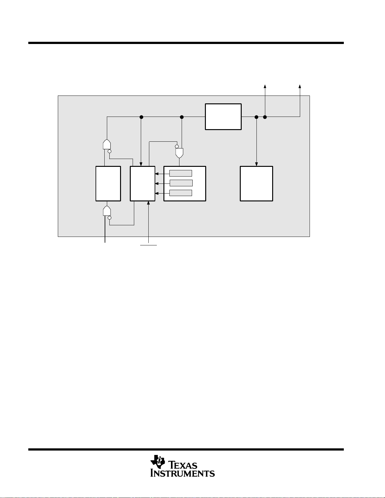
functional block and CPU (DSP core) diagram
SDRAM
SBSRAM
SRAM
ROM/FLASH
I/O Devices
Framing Chips:
H.100, MVIP,
SCSA, T1, E1
AC97 Devices,
SPI Devices,
Codecs
32
16
External
Memory
Interface
(EMIF)
Timer 0
Timer 1
Multichannel
Buffered
Serial Port 1
(McBSP1)
Multichannel
Buffered
Serial Port 0
(McBSP0)
Host Port
Interface
(HPI)
Interrupt
Selector
Enhanced
DMA
Controller
(16 channel)
L2
Memory
4 Banks
64K Bytes
Total
PLL
(x1, x4)
C6211/C6211B Digital Signal Processors
L1P Cache
Direct Mapped
4K Bytes Total
C6000 CPU (DSP Core)
Instruction Fetch
Instruction Dispatch
Instruction Decode
Data Path A
A Register File
.L1 .S1 .M1 .D1 .D2 .M2 .S2 .L2
Power-Down
Logic
Data Path B
B Register File
L1D Cache
2-Way Set
Associative
4K Bytes Total
Boot
Configuration
Control
Registers
Control
Logic
Test
In-Circuit
Emulation
Interrupt
Control
6
POST OFFICE BOX 1443 • HOUSTON, TEXAS 77251−1443

TMS320C6211, TMS320C6211B
FIXED-POINT DIGITAL SIGNAL PROCESSORS
SPRS073K − AUGUST 1998 − REVISED MARCH 2004
CPU (DSP core) description
The CPU fetches VelociTI advanced very-long instruction words (VLIW) (256 bits wide) to supply up to eight
32-bit instructions to the eight functional units during every clock cycle. The VelociTI VLIW architecture
features controls by which all eight units do not have to be supplied with instructions if they are not ready to
execute. The first bit of every 32-bit instruction determines if the next instruction belongs to the same execute
packet as the previous instruction, or whether it should be executed in the following clock as a part of the next
execute packet. Fetch packets are always 256 bits wide; however, the execute packets can vary in size. The
variable-length execute packets are a key memory-saving feature, distinguishing the C62x CPU from other
VLIW architectures.
The CPU features two sets of functional units. Each set contains four units and a register file. One set contains
functional units .L1, .S1, .M1, and .D1; the other set contains units .D2, .M2, .S2, and .L2. The two register files
each contain 16 32-bit registers for a total of 32 general-purpose registers. The two sets of functional units, along
with two register files, compose sides A and B of the CPU (see the functional block and CPU diagram and
Figure 1). The four functional units on each side of the CPU can freely share the 16 registers belonging to that
side. Additionally, each side features a single data bus connected to all the registers on the other side, by which
the two sets of functional units can access data from the register files on the opposite side. While register access
by functional units on the same side of the CPU as the register file can service all the units in a single clock cycle,
register access using the register file across the CPU supports one read and one write per cycle.
Another key feature of the C62x CPU is the load/store architecture, where all instructions operate on registers
(as opposed to data in memory). Two sets of data-addressing units (.D1 and .D2) are responsible for all data
transfers between the register files and the memory. The data address driven by the .D units allows data
addresses generated from one register file to be used to load or store data to or from the other register file. The
C62x CPU supports a variety of indirect addressing modes using either linear- or circular-addressing modes
with 5- or 15-bit offsets. All instructions are conditional, and most can access any one of the 32 registers. Some
registers, however, are singled out to support specific addressing or to hold the condition for conditional
instructions (if the condition is not automatically “true”). The two .M functional units are dedicated for multiplies.
The two .S and .L functional units perform a general set of arithmetic, logical, and branch functions with results
available every clock cycle.
The processing flow begins when a 256-bit-wide instruction fetch packet is fetched from a program memory.
The 32-bit instructions destined for the individual functional units are “linked” together by “1” bits in the least
significant bit (LSB) position of the instructions. The instructions that are “chained” together for simultaneous
execution (up to eight in total) compose an execute packet. A “0” in the LSB of an instruction breaks the chain,
effectively placing the instructions that follow it in the next execute packet. If an execute packet crosses the
fetch-packet boundary (256 bits wide), the assembler places it in the next fetch packet, while the remainder of
the current fetch packet is padded with NOP instructions. The number of execute packets within a fetch packet
can vary from one to eight. Execute packets are dispatched to their respective functional units at the rate of one
per clock cycle and the next 256-bit fetch packet is not fetched until all the execute packets from the current fetch
packet have been dispatched. After decoding, the instructions simultaneously drive all active functional units
for a maximum execution rate of eight instructions every clock cycle. While most results are stored in 32-bit
registers, they can be subsequently moved to memory as bytes or half-words as well. All load and store
instructions are byte-, half-word, or word-addressable.
POST OFFICE BOX 1443 • HOUSTON, TEXAS 77251−1443
7
TMS320C6211, TMS320C6211B
FIXED-POINT DIGITAL SIGNAL PROCESSORS
SPRS073K − AUGUST 1998 − REVISED MARCH 2004
CPU (DSP core) description (continued)
ST1
Data Path A
LD1
DA1
DA2
LD2
.L1
long dst
long src
long src
long dst
.S1
.M1
.D1
.D2
.M2
src1
src2
dst
dst
src1
src2
dst
src1
src2
dst
src1
src2
src2
src1
dst
src2
src1
dst
8
8
32
8
Register
File A
(A0−A15)
2X
1X
Data Path B
Figure 1. TMS320C62x CPU (DSP Core) Data Paths
ST2
.S2
long dst
long src
long src
long dst
.L2
src2
src1
dst
dst
src2
src1
Register
File B
(B0−B15)
8
32
8
8
Control
Register
File
8
POST OFFICE BOX 1443 • HOUSTON, TEXAS 77251−1443
TMS320C6211, TMS320C6211B
FIXED-POINT DIGITAL SIGNAL PROCESSORS
SPRS073K − AUGUST 1998 − REVISED MARCH 2004
memory map summary
Table 2 shows the memory map address ranges of the C6211/C6211B devices. Internal memory is always
located at address 0 and can be used as both program and data memory. The C6211/C6211B configuration
registers for the common peripherals are located at the same hex address ranges. The external memory
address ranges in the C6211/C6211B devices begin at the address location 0x8000 0000.
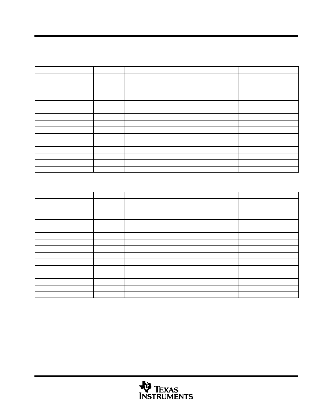
Table 2. TMS320C6211/C6211B Memory Map Summary
MEMORY BLOCK DESCRIPTION BLOCK SIZE (BYTES) HEX ADDRESS RANGE
Internal RAM (L2) 64K 0000 0000 – 0000 FFFF
Reserved 24M – 64K 0001 0000 – 017F FFFF
External Memory Interface (EMIF) Registers 256K 0180 0000 – 0183 FFFF
L2 Registers 256K 0184 0000 – 0187 FFFF
HPI Registers 256K 0188 0000 – 018B FFFF
McBSP 0 Registers 256K 018C 0000 – 018F FFFF
McBSP 1 Registers 256K 0190 0000 – 0193 FFFF
Timer 0 Registers 256K 0194 0000 – 0197 FFFF
Timer 1 Registers 256K 0198 0000 – 019B FFFF
Interrupt Selector Registers 256K 019C 0000 – 019F FFFF
EDMA RAM and EDMA Registers 256K 01A0 0000 – 01A3 FFFF
Reserved 6M – 256K 01A4 0000 – 01FF FFFF
QDMA Registers 52 0200 0000 – 0200 0033
Reserved 736M – 52 0200 0034 – 2FFF FFFF
McBSP 0/1 Data 256M 3000 0000 – 3FFF FFFF
Reserved 1G 4000 0000 – 7FFF FFFF
EMIF CE0
EMIF CE1
EMIF CE2
EMIF CE3
Reserved 1G C000 0000 – FFFF FFFF
†
The number of EMIF address pins (EA[21:2]) limits the maximum addressable memory (SDRAM) to 128MB per CE space. To get 256MB of
addressable memory, additional general-purpose output pin or external logic is required.
†
†
†
†
256M 8000 0000 – 8FFF FFFF
256M 9000 0000 – 9FFF FFFF
256M A000 0000 – AFFF FFFF
256M B000 0000 – BFFF FFFF
POST OFFICE BOX 1443 • HOUSTON, TEXAS 77251−1443
9
TMS320C6211, TMS320C6211B
FIXED-POINT DIGITAL SIGNAL PROCESSORS
SPRS073K − AUGUST 1998 − REVISED MARCH 2004
peripheral register descriptions
Table 3 through Table 13 identify the peripheral registers for the C6211/C6211B device by their register names,
acronyms, and hex address or hex address range. For more detailed information on the register contents, bit
names, and their descriptions, see the TMS320C6000 DSP Peripherals Overview Reference Guide (literature
number SPRU190).
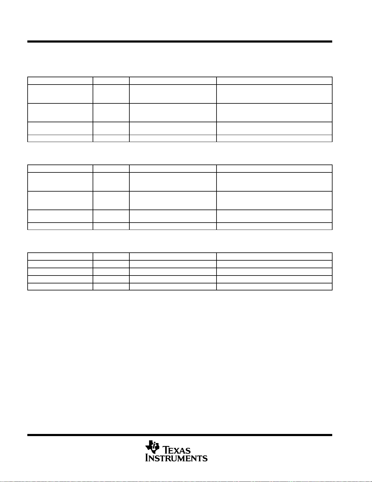
Table 3. EMIF Registers
HEX ADDRESS RANGE ACRONYM REGISTER NAME
0180 0000 GBLCTL EMIF global control
0180 0004 CECTL1 EMIF CE1 space control
0180 0008 CECTL0 EMIF CE0 space control
0180 000C − Reserved
0180 0010 CECTL2 EMIF CE2 space control
0180 0014 CECTL3 EMIF CE3 space control
0180 0018 SDCTL EMIF SDRAM control
0180 001C SDTIM EMIF SDRAM refresh control
0180 0020 SDEXT EMIF SDRAM extension
0180 0024 − 0183 FFFF − Reserved
Table 4. L2 Cache Registers
HEX ADDRESS RANGE ACRONYM REGISTER NAME
0184 0000 CCFG Cache configuration register
0184 4000 L2FBAR L2 flush base address register
0184 4004 L2FWC L2 flush word count register
0184 4010 L2CBAR L2 clean base address register
0184 4014 L2CWC L2 clean word count register
0184 4020 L1PFBAR L1P flush base address register
0184 4024 L1PFWC L1P flush word count register
0184 4030 L1DFBAR L1D flush base address register
0184 4034 L1DFWC L1D flush word count register
0184 5000 L2FLUSH L2 flush register
0184 5004 L2CLEAN L2 clean register
0184 8200 MAR0 Controls CE0 range 8000 0000 − 80FF FFFF
0184 8204 MAR1 Controls CE0 range 8100 0000 − 81FF FFFF
0184 8208 MAR2 Controls CE0 range 8200 0000 − 82FF FFFF
0184 820C MAR3 Controls CE0 range 8300 0000 − 83FF FFFF
0184 8240 MAR4 Controls CE1 range 9000 0000 − 90FF FFFF
0184 8244 MAR5 Controls CE1 range 9100 0000 − 91FF FFFF
0184 8248 MAR6 Controls CE1 range 9200 0000 − 92FF FFFF
0184 824C MAR7 Controls CE1 range 9300 0000 − 93FF FFFF
0184 8280 MAR8 Controls CE2 range A000 0000 − A0FF FFFF
0184 8284 MAR9 Controls CE2 range A100 0000 − A1FF FFFF
0184 8288 MAR10 Controls CE2 range A200 0000 − A2FF FFFF
0184 828C MAR11 Controls CE2 range A300 0000 − A3FF FFFF
0184 82C0 MAR12 Controls CE3 range B000 0000 − B0FF FFFF
0184 82C4 MAR13 Controls CE3 range B100 0000 − B1FF FFFF
0184 82C8 MAR14 Controls CE3 range B200 0000 − B2FF FFFF
0184 82CC MAR15 Controls CE3 range B300 0000 − B3FF FFFF
0184 82D0 − 0187 FFFF − Reserved
10
POST OFFICE BOX 1443 • HOUSTON, TEXAS 77251−1443
TMS320C6211, TMS320C6211B
FIXED-POINT DIGITAL SIGNAL PROCESSORS
SPRS073K − AUGUST 1998 − REVISED MARCH 2004
peripheral register descriptions (continued)
Table 5. EDMA Registers
HEX ADDRESS RANGE ACRONYM REGISTER NAME
01A0 FF9C − 01A0 FFDC − Reserved
01A0 FFE0 PQSR Priority queue status register
01A0 FFE4 CIPR Channel interrupt pending register
01A0 FFE8 CIER Channel interrupt enable register
01A0 FFEC CCER Channel chain enable register
01A0 FFF0 ER Event register
01A0 FFF4 EER Event enable register
01A0 FFF8 ECR Event clear register
01A0 FFFC ESR Event set register
01A1 0000 − 01A3 FFFF – Reserved
Table 6. EDMA Parameter RAM
HEX ADDRESS RANGE
01A0 0000 − 01A0 0017 − Parameters for Event 0 (6 words)
01A0 0018 − 01A0 002F − Parameters for Event 1 (6 words)
01A0 0030 − 01A0 0047 − Parameters for Event 2 (6 words)
01A0 0048 − 01A0 005F − Parameters for Event 3 (6 words)
01A0 0060 − 01A0 0077 − Parameters for Event 4 (6 words)
01A0 0078 − 01A0 008F − Parameters for Event 5 (6 words)
01A0 0090 − 01A0 00A7 − Parameters for Event 6 (6 words)
01A0 00A8 − 01A0 00BF − Parameters for Event 7 (6 words)
01A0 00C0 − 01A0 00D7 − Parameters for Event 8 (6 words)
01A0 00D8 − 01A0 00EF − Parameters for Event 9 (6 words)
01A0 00F0 − 01A0 00107 − Parameters for Event 10 (6 words)
01A0 0108 − 01A0 011F − Parameters for Event 11 (6 words)
01A0 0120 − 01A0 0137 − Parameters for Event 12 (6 words)
01A0 0138 − 01A0 014F − Parameters for Event 13 (6 words)
01A0 0150 − 01A0 0167 − Parameters for Event 14 (6 words)
01A0 0168 − 01A0 017F − Parameters for Event 15 (6 words)
01A0 0180 − 01A0 0197 − Reload/link parameters for Event M (6 words)
01A0 0198 − 01A0 01AF − Reload/link parameters for Event N (6 words)
... ...
01A0 07E0 − 01A0 07F7 − Reload/link parameters for Event Z (6 words)
01A0 07F8 − 01A0 07FF − Scratch pad area (2 words)
†
The C6211/C6211B device has sixty-nine parameter sets [six (6) words each] that can be used to reload/link EDMA transfers.
ACRONYM REGISTER NAME
†
POST OFFICE BOX 1443 • HOUSTON, TEXAS 77251−1443
11
TMS320C6211, TMS320C6211B
FIXED-POINT DIGITAL SIGNAL PROCESSORS
SPRS073K − AUGUST 1998 − REVISED MARCH 2004
peripheral register descriptions (continued)
Table 7. Quick DMA (QDMA) and Pseudo Registers
HEX ADDRESS RANGE
0200 0000 QOPT QDMA options parameter register
0200 0004 QSRC QDMA source address register
0200 0008 QCNT QDMA frame count register
0200 000C QDST QDMA destination address register
0200 0010 QIDX QDMA index register
0200 0014 − 0200 001C − Reserved
0200 0020 QSOPT QDMA pseudo options register
0200 0024 QSSRC QDMA pseudo source address register
0200 0028 QSCNT QDMA pseudo frame count register
0200 002C QSDST QDMA pseudo destination address register
0200 0030 QSIDX QDMA pseudo index register
†
All the QDMA and Pseudo registers are write-accessible only
ACRONYM REGISTER NAME
†
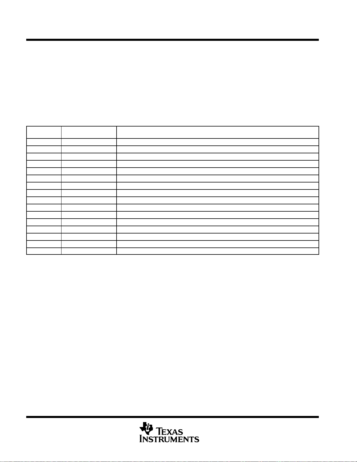
Table 8. Interrupt Selector Registers
HEX ADDRESS RANGE ACRONYM REGISTER NAME COMMENTS
019C 0000 MUXH Interrupt multiplexer high
019C 0004 MUXL Interrupt multiplexer low
019C 0008 EXTPOL External interrupt polarity
019C 000C − 019F FFFF − Reserved
Selects which interrupts drive CPU interrupts
10−15 (INT10−INT15)
Selects which interrupts drive CPU interrupts 4−9
(INT04−INT09)
Sets the polarity of the external interrupts
(EXT_INT4−EXT_INT7)
12
POST OFFICE BOX 1443 • HOUSTON, TEXAS 77251−1443
TMS320C6211, TMS320C6211B
FIXED-POINT DIGITAL SIGNAL PROCESSORS
SPRS073K − AUGUST 1998 − REVISED MARCH 2004
peripheral register descriptions (continued)
Table 9. McBSP 0 Registers
HEX ADDRESS RANGE ACRONYM REGISTER NAME COMMENTS
The CPU and DMA/EDMA
018C 0000 DRR0 McBSP0 data receive register via Peripheral Bus
0x3000 0000 − 0x33FF FFFF DRR0 McBSP0 data receive register via EDMA Bus
018C 0004 DXR0 McBSP0 data transmit register via Peripheral Bus
0x3000 0000 − 0x33FF FFFF DXR0 McBSP0 data transmit register via EDMA Bus
018C 0008 SPCR0 McBSP0 serial port control register
018C 000C RCR0 McBSP0 receive control register
018C 0010 XCR0 McBSP0 transmit control register
018C 0014 SRGR0 McBSP0 sample rate generator register
018C 0018 MCR0 McBSP0 multichannel control register
018C 001C RCER0 McBSP0 receive channel enable register
018C 0020 XCER0 McBSP0 transmit channel enable register
018C 0024 PCR0 McBSP0 pin control register
018C 0028 − 018F FFFF − Reserved
controller can only read this
register; they cannot write to
it.
Table 10. McBSP 1 Registers
HEX ADDRESS RANGE ACRONYM REGISTER NAME COMMENTS
The CPU and DMA/EDMA
0190 0000 DRR1 Data receive register via Peripheral Bus
0x3400 0000 − 0x37FF FFFF DRR1 McBSP1 data receive register via EDMA Bus
0190 0004 DXR1 McBSP1 data transmit register via Peripheral Bus
0x3400 0000 − 0x37FF FFFF DXR1 McBSP1 data transmit register via EDMA Bus
0190 0008 SPCR1 McBSP1 serial port control register
0190 000C RCR1 McBSP1 receive control register
0190 0010 XCR1 McBSP1 transmit control register
0190 0014 SRGR1 McBSP1 sample rate generator register
0190 0018 MCR1 McBSP1 multichannel control register
0190 001C RCER1 McBSP1 receive channel enable register
0190 0020 XCER1 McBSP1 transmit channel enable register
0190 0024 PCR1 McBSP1 pin control register
0190 0028 − 0193 FFFF − Reserved
controller can only read this
register; they cannot write to
it.
POST OFFICE BOX 1443 • HOUSTON, TEXAS 77251−1443
13
TMS320C6211, TMS320C6211B
FIXED-POINT DIGITAL SIGNAL PROCESSORS
SPRS073K − AUGUST 1998 − REVISED MARCH 2004
peripheral register descriptions (continued)
Table 11. Timer 0 Registers
HEX ADDRESS RANGE ACRONYM REGISTER NAME COMMENTS
Determines the operating mode of the timer,
0194 0000 CTL0 Timer 0 control register
0194 0004 PRD0 Timer 0 period register
0194 0008 CNT0 Timer 0 counter register
0194 000C − 0197 FFFF − Reserved
Table 12. Timer 1 Registers
HEX ADDRESS RANGE ACRONYM REGISTER NAME COMMENTS
0198 0000 CTL1 Timer 1 control register
0198 0004 PRD1 Timer 1 period register
0198 0008 CNT1 Timer 1 counter register
0198 000C − 019B FFFF − Reserved
monitors the timer status, and controls the function
of the TOUT pin.
Contains the number of timer input clock cycles to
count. This number controls the TSTAT signal
frequency.
Contains the current value of the incrementing
counter.
Determines the operating mode of the timer,
monitors the timer status, and controls the function
of the TOUT pin.
Contains the number of timer input clock cycles to
count. This number controls the TSTAT signal
frequency.
Contains the current value of the incrementing
counter.
Table 13. HPI Registers
HEX ADDRESS RANGE ACRONYM REGISTER NAME COMMENTS
− HPID HPI data register Host read/write access only
− HPIA HPI address register Host read/write access only
0188 0000 HPIC HPI control register Both Host/CPU read/write access
0188 0001 − 018B FFFF − Reserved
14
POST OFFICE BOX 1443 • HOUSTON, TEXAS 77251−1443
TMS320C6211, TMS320C6211B
FIXED-POINT DIGITAL SIGNAL PROCESSORS
SPRS073K − AUGUST 1998 − REVISED MARCH 2004
PWRD bits in CPU CSR register description
Table 14 identifies the PWRD field (bits 15−10) in the CPU CSR register. These bits control the device
power-down modes. For more detailed information on the PWRD bit field of the CPU CSR register, see the
TMS320C6000 CPU and Instruction Set Reference Guide (literature number SPRU189).
Table 14. PWRD field bits in the CPU CSR Register
HEX ADDRESS RANGE ACRONYM REGISTER NAME COMMENTS
The PWRD field (bits 15−10 in the CPU CSR)
− CSR Control status register
controls the device power-down modes.
Accessible by writing a value to the CSR register.
POST OFFICE BOX 1443 • HOUSTON, TEXAS 77251−1443
15
TMS320C6211, TMS320C6211B
FIXED-POINT DIGITAL SIGNAL PROCESSORS
SPRS073K − AUGUST 1998 − REVISED MARCH 2004
EDMA channel synchronization events
The C62x EDMA supports up to 16 EDMA channels. Four of the sixteen channels (channels 8−11) are reserved
for EDMA chaining, leaving 12 EDMA channels available to service peripheral devices. Table 15 lists the source
of synchronization events associated with each of the programmable EDMA channels. For the C6211/11B, the
association of an event to a channel is fixed; each of the EDMA channels has one specific event associated
with it. For more detailed information on the EDMA module, associated channels, and event-transfer chaining,
see the TMS320C6000 DSP Enhanced Direct Memory Access (EDMA) Controller Reference Guide (literature
number SPRU234).
Table 15. TMS320C6211/C6211B EDMA Channel Synchronization Events
EDMA
CHANNEL
0 DSP_INT Host-port interface (HPI)-to-DSP interrupt
1 TINT0 Timer 0 interrupt
2 TINT1 Timer 1 interrupt
3 SD_INT EMIF SDRAM timer interrupt
4 EXT_INT4 External interrupt pin 4
5 EXT_INT5 External interrupt pin 5
6 EXT_INT6 External interrupt pin 6
7 EXT_INT7 External interrupt pin 7
†
8
†
9
†
10
†
11
12 XEVT0 McBSP0 transmit event
13 REVT0 McBSP0 receive event
14 XEVT1 McBSP1 transmit event
15 REVT1 McBSP1 receive event
†
EDMA channels 8 through 11 are used for transfer chaining only. For more detailed information on event-transfer chaining, see the
TMS320C6000 DSP Enhanced Direct Memory Access (EDMA) Controller Reference Guide (literature number SPRU234).
EVENT NAME EVENT DESCRIPTION
EDMA_TCC8 EDMA transfer complete code (TCC) 1000b interrupt
EDMA_TCC9 EDMA TCC 1001b interrupt
EDMA_TCC10 EDMA TCC 1010b interrupt
EDMA_TCC11 EDMA TCC 1011b interrupt
16
POST OFFICE BOX 1443 • HOUSTON, TEXAS 77251−1443
TMS320C6211, TMS320C6211B
FIXED-POINT DIGITAL SIGNAL PROCESSORS
SPRS073K − AUGUST 1998 − REVISED MARCH 2004
interrupt sources and interrupt selector
The C62x DSP core supports 16 prioritized interrupts, which are listed in Table 16. The highest-priority interrupt
is INT_00 (dedicated to RESET) while the lowest-priority interrupt is INT_15. The first four interrupts
(INT_00−INT_03) are non-maskable and fixed. The remaining interrupts (INT_04−INT_15) are maskable and
default to the interrupt source specified in Table 16. The interrupt source for interrupts 4−15 can be programmed
by modifying the selector value (binary value) in the corresponding fields of the Interrupt Selector Control
registers: MUXH (address 0x019C0000) and MUXL (address 0x019C0004).
Table 16. C6211/C6211B DSP Interrupts
CPU
INTERRUPT
NUMBER
†
INT_00
†
INT_01
†
INT_02
†
INT_03
‡
INT_04
‡
INT_05
‡
INT_06
‡
INT_07
‡
INT_08
‡
INT_09
‡
INT_10
‡
INT_11
‡
INT_12
‡
INT_13
‡
INT_14
‡
INT_15
− − 01100 XINT0 McBSP0 transmit interrupt
− − 01101 RINT0 McBSP0 receive interrupt
− − 01110 XINT1 McBSP1 transmit interrupt
− − 0 1111 RINT1 McBSP1 receive interrupt
− − 10000 − 11111 Reserved Reserved. Do not use.
†
Interrupts INT_00 through INT_03 are non-maskable and fixed.
‡
Interrupts INT_04 through INT_15 are programmable by modifying the binary selector values in the Interrupt Selector Control
registers fields. Table 16 shows the default interrupt sources for Interrupts INT_04 through INT_15. For more detailed
information on interrupt sources and selection, see the TMS320C6000 DSP Interrupt Selector Reference Guide (literature
number SPRU646).
INTERRUPT
SELECTOR
CONTROL
REGISTER
SELECTOR
VALUE
(BINARY)
INTERRUPT
EVENT
INTERRUPT SOURCE
− − RESET
− − NMI
− − Reserved Reserved. Do not use.
− − Reserved Reserved. Do not use.
MUXL[4:0] 00100 EXT_INT4 External interrupt pin 4
MUXL[9:5] 00101 EXT_INT5 External interrupt pin 5
MUXL[14:10] 00110 EXT_INT6 External interrupt pin 6
MUXL[20:16] 00111 EXT_INT7 External interrupt pin 7
MUXL[25:21] 01000 EDMA_INT EDMA channel (0 through 15) interrupt
MUXL[30:26] 01001 Reserved None, but programmable
MUXH[4:0] 00011 SD_INT EMIF SDRAM timer interrupt
MUXH[9:5] 01010 Reserved None, but programmable
MUXH[14:10] 01011 Reserved None, but programmable
MUXH[20:16] 00000 DSP_INT Host-port interface (HPI)-to-DSP interrupt
MUXH[25:21] 00001 TINT0 Timer 0 interrupt
MUXH[30:26] 00010 TINT1 Timer 1 interrupt
POST OFFICE BOX 1443 • HOUSTON, TEXAS 77251−1443
17
TMS320C6211, TMS320C6211B
FIXED-POINT DIGITAL SIGNAL PROCESSORS
SPRS073K − AUGUST 1998 − REVISED MARCH 2004
signal groups description
CLKIN
CLKOUT2
CLKOUT1
CLKMODE0
PLLV
PLLG
PLLF
TMS
TDO
TDI
TCK
TRST
EMU0
EMU1
EMU2
EMU3
EMU4
EMU5
Clock/PLL
IEEE Standard
1149.1
(JTAG)
Emulation
Control/Status
Reset and
Interrupts
Reserved
RESET
NMI
EXT_INT7
EXT_INT6
EXT_INT5
EXT_INT4
RSV5
RSV4
RSV3
RSV2
RSV1
RSV0
HD[15:0]
HCNTL0
HCNTL1
HHWIL
16
Data
Register Select
Half-Word
Select
(Host-Port Interface)
HPI
Control
Figure 2. CPU (DSP Core) and Peripheral Signals
HAS
HR/W
HCS
HDS1
HDS2
HRDY
HINT
18
POST OFFICE BOX 1443 • HOUSTON, TEXAS 77251−1443
signal groups description (continued)
TMS320C6211, TMS320C6211B
FIXED-POINT DIGITAL SIGNAL PROCESSORS
SPRS073K − AUGUST 1998 − REVISED MARCH 2004
ED[31:0]
CE3
CE2
CE1
CE0
EA[21:2]
BE3
BE2
BE1
BE0
TOUT1
TINP1
32
20
Data
Memory Map
Space Select
Address
Byte Enables
Timer 1
Memory
Control
Bus
Arbitration
EMIF
(External Memory Interface)
Timer 0
Timers
ECLKIN
ECLKOUT
ARE/SDCAS/SSADS
AOE
/SDRAS/SSOE
AWE/SDWE/SSWE
ARDY
HOLD
HOLDA
BUSREQ
TOUT0
TINP0
CLKX1
FSX1
DX1
CLKR1
FSR1
DR1
CLKS1
McBSP1 McBSP0
Transmit Transmit
Receive Receive
Clock Clock
McBSPs
(Multichannel Buffered Serial Ports)
Figure 3. Peripheral Signals
CLKX0
FSX0
DX0
CLKR0
FSR0
DR0
CLKS0
POST OFFICE BOX 1443 • HOUSTON, TEXAS 77251−1443
19
TMS320C6211, TMS320C6211B
†
IPD/
DESCRIPTION
E
l i
g
• Edge-driven
yp y p yg
FIXED-POINT DIGITAL SIGNAL PROCESSORS
SPRS073K − AUGUST 1998 − REVISED MARCH 2004
Terminal Functions
SIGNAL
NAME NO.
TYPE
CLKIN A3 I IPD Clock Input
CLKOUT1 D7 O IPD
CLKOUT2 Y12 O IPD
CLKMODE0 C4 I IPU
§
PLLV
PLLG
§
A4 A
C6 A
PLLF B5 A
TMS B7 I IPU JTAG test-port mode select
TDO A8 O/Z IPU JTAG test-port data out
TDI A7 I IPU JTAG test-port data in
TCK A6 I IPU JTAG test-port clock
TRST B6 I IPD JTAG test-port reset
EMU5 B12 I/O/Z IPU Emulation pin 5. Reserved for future use, leave unconnected.
EMU4 C11 I/O/Z IPU Emulation pin 4. Reserved for future use, leave unconnected.
EMU3 B10 I/O/Z IPU Emulation pin 3. Reserved for future use, leave unconnected.
EMU2 D10 I/O/Z IPU Emulation pin 2. Reserved for future use, leave unconnected.
EMU1 B9 I/O/Z IPU Emulation pin 1
EMU0 D9 I/O/Z IPU Emulation pin 0
RESET A13 I IPU Device reset
NMI C13 I IPD
EXT_INT7 E3
EXT_INT6 D2
EXT_INT5 C1
EXT_INT4 C2
HINT J20 O IPU Host interrupt (from DSP to host)
HCNTL1 G19 I IPU Host control − selects between control, address, or data registers
HCNTL0 G18 I IPU Host control − selects between control, address, or data registers
HHWIL H20 I IPU Host half-word select − first or second half-word (not necessarily high or low order)
HR/W G20 I IPU Host read or write select
†
I = Input, O = Output, Z = High impedance, S = Supply voltage, GND = Ground
‡
IPD = Internal pulldown, IPU = Internal pullup. (These IPD/IPU signal pins feature a 30-kΩ IPD or IPU resistor. To pull up a signal to the opposite
supply rail, a 1-kΩ resistor should be used.)
IPD/
IPU
¶
¶
¶
I IPU
‡
CLOCK/PLL
Clock output at device speed
The CLK1EN bit in the EMIF GBLCTL register controls the CLKOUT1 pin.
CLK1EN = 0: CLKOUT1 is disabled
CLK1EN = 1: CLKOUT1 enabled to clock [default]
Clock output at half of device speed
When the CLKOUT2 pin is enabled, the CLK2EN bit in the EMIF global control register
(GBLCTL) controls the CLKOUT2 pin.
CLK2EN = 0: CLKOUT2 is disabled
CLK2EN = 1: CLKOUT1 enabled to clock [default]
Clock mode select
• Selects whether the CPU clock frequency = input clock frequency x4 or x1
PLL analog VCC connection for the low-pass filter
PLL analog GND connection for the low-pass filter
PLL low-pass filter connection to external components and a bypass capacitor
JTAG EMULATION
#
#
RESETS AND INTERRUPTS
Nonmaskable interrupt
• Edge-driven (rising edge)
Any noise on the NMI pin may trigger an NMI interrupt; therefore, if the NMI pin is not used, it is
recommended that the NMI pin be grounded versus relying on the IPD.
xterna
• Ed
nterrupts
e-driven
• Polarity independently selected via the External Interrupt Polarity Register bits
(EXTPOL.[3:0])
HOST-PORT INTERFACE (HPI)
20
POST OFFICE BOX 1443 • HOUSTON, TEXAS 77251−1443
TMS320C6211, TMS320C6211B
IPD/
Also controls initialization of DSP modes at reset via pullup/pulldown resistors
Device Endian mode
Boot mode
HD[4:3]: 00 HPI boot
11−32-bit ROM boot with default timings
Only one asserted d
access
• Only one asserted during any external data access
B
l
• Decoded from the two lowest bits of the internal address
yypy
FIXED-POINT DIGITAL SIGNAL PROCESSORS
SPRS073K − AUGUST 1998 − REVISED MARCH 2004
§
PLLV and PLLG are not part of external voltage supply or ground. See the CLOCK/PLL documentation for information on how to connect these
pins.
¶
A = Analog signal (PLL Filter)
#
The EMU0 and EMU1 pins are internally pulled up with 30-kΩ resistors; therefore, for emulation and normal operation, no external
pullup/pulldown resistors are necessary. However, for boundary scan operation, pull down the EMU1 and EMU0 pins with a dedicated 1-kΩ
resistor.
Terminal Functions (Continued)
SIGNAL
NAME NO.
TYPE
HD15 B14 IPU
HD14 C14 IPU
HD13 A15 IPU
HD12 C15 IPU
HD11 A16 IPU
HD10 B16 IPU
HD9 C16 IPU
HD8 B17
HD7 A18
I/O/Z
HD6 C17 IPU
HD5 B18 IPU
HD4 C19 IPD
HD3 C20 IPU
HD2 D18 IPU
HD1 D20 IPU
HD0 E20 IPU
HAS E18 I IPU Host address strobe
HCS F20 I IPU Host chip select
HDS1 E19 I IPU Host data strobe 1
HDS2 F18 I IPU Host data strobe 2
HRDY H19 O IPD Host ready (from DSP to host)
CE3 V6 O/Z IPU
CE2 W6 O/Z IPU
CE1 W18 O/Z IPU
CE0 V17 O/Z IPU
BE3 V5 O/Z IPU
BE2 Y4 O/Z IPU
BE1 U19 O/Z IPU
BE0 V20 O/Z IPU
†
I = Input, O = Output, Z = High impedance, S = Supply voltage, GND = Ground
‡
IPD = Internal pulldown, IPU = Internal pullup. (These IPD/IPU signal pins feature a 30-kΩ IPD or IPU resistor. To pull up a signal to the opposite
supply rail, a 1-kΩ resistor should be used.)
IPD/
†
IPU‡
DESCRIPTION
HOST-PORT INTERFACE (HPI) (CONTINUED)
Host-port data
• Used for transfer of data, address, and control
•
− Device Endian mode
IPU
IPU
HD8: 0 – Big Endian
1 − Little Endian
−
−
HD[4:3]: 00 – HPI boot
01 − 8-bit ROM boot with default timings
10 − 16-bit ROM boot with default timings
11 −
2-i R
M
wih fl
imin
EMIF − CONTROL SIGNALS COMMON TO ALL TYPES OF MEMORY
Memory space enables
• Enabled by bits 28 through 31 of the word address
•
uring any external data
yte-enable contro
• Decoded from the two lowest bits of the internal address
• Byte-write enables for most types of memory
• Can be directly connected to SDRAM read and write mask signal (SDQM)
POST OFFICE BOX 1443 • HOUSTON, TEXAS 77251−1443
21
TMS320C6211, TMS320C6211B
/
IPD/
FIXED-POINT DIGITAL SIGNAL PROCESSORS
SPRS073K − AUGUST 1998 − REVISED MARCH 2004
Terminal Functions (Continued)
SIGNAL
NAME NO.
HOLDA J18 O IPU Hold-request-acknowledge to the host
HOLD J17 I IPU Hold request from the host
BUSREQ J19 O IPU Bus request output
EMIF − ASYNCHRONOUS/SYNCHRONOUS DRAM/SYNCHRONOUS BURST SRAM MEMORY CONTROL
ECLKIN Y11 I IPD EMIF input clock
ECLKOUT Y10 O IPD EMIF output clock (based on ECLKIN)
ARE/SDCAS/
SSADS
AOE/SDRAS/
SSOE
AWE/SDWE/
SSWE
ARDY Y5 I IPU Asynchronous memory ready input
EA21 U18
EA20 Y18
EA19 W17
EA18 Y16
EA17 V16
EA16 Y15
EA15 W15
EA14 Y14
EA13 W14
EA12 V14
EA11 W13
EA10 V10
EA9 Y9
EA8 V9
EA7 Y8
EA6 W8
EA5 V8
EA4 W7
EA3 V7
EA2 Y6
†
I = Input, O = Output, Z = High impedance, S = Supply voltage, GND = Ground
‡
IPD = Internal pulldown, IPU = Internal pullup. (These IPD/IPU signal pins feature a 30-kΩ IPD or IPU resistor. To pull up a signal to the opposite
supply rail, a 1-kΩ resistor should be used.)
V11 O/Z IPU Asynchronous memory read enable/SDRAM column-address strobe/SBSRAM address strobe
W10 O/Z IPU Asynchronous memory output enable/SDRAM row-address strobe/SBSRAM output enable
V12 O/Z IPU Asynchronous memory write enable/SDRAM write enable/SBSRAM write enable
TYPE
O/Z IPU EMIF external address
IPD
†
IPU
‡
EMIF − BUS ARBITRATION
EMIF − ADDRESS
DESCRIPTION
22
POST OFFICE BOX 1443 • HOUSTON, TEXAS 77251−1443
TMS320C6211, TMS320C6211B
IPD/
FIXED-POINT DIGITAL SIGNAL PROCESSORS
SPRS073K − AUGUST 1998 − REVISED MARCH 2004
Terminal Functions (Continued)
SIGNAL
NAME NO.
ED31 N3
ED30 P3
ED29 P2
ED28 P1
ED27 R2
ED26 R3
ED25 T2
ED24 T1
ED23 U3
ED22 U1
ED21 U2
ED20 V1
ED19 V2
ED18 Y3
ED17 W4
ED16 V4
ED15 T19
ED14 T20
ED13 T18
ED12 R20
ED11 R19
ED10 P20
ED9 P18
ED8 N20
ED7 N19
ED6 N18
ED5 M20
ED4 M19
ED3 L19
ED2 L18
ED1 K19
ED0 K18
†
I = Input, O = Output, Z = High impedance, S = Supply voltage, GND = Ground
‡
IPD = Internal pulldown, IPU = Internal pullup. (These IPD/IPU signal pins feature a 30-kΩ IPD or IPU resistor. To pull up a signal to the opposite
supply rail, a 1-kΩ resistor should be used.)
TYPE
I/O/Z IPU External data
IPD/
†
IPU‡
EMIF − DATA
DESCRIPTION
POST OFFICE BOX 1443 • HOUSTON, TEXAS 77251−1443
23
TMS320C6211, TMS320C6211B
IPD/
FIXED-POINT DIGITAL SIGNAL PROCESSORS
SPRS073K − AUGUST 1998 − REVISED MARCH 2004
Terminal Functions (Continued)
SIGNAL
NAME NO.
TOUT1 F1 O IPD Timer 1 or general-purpose output
TINP1 F2 I IPD Timer 1 or general-purpose input
TOUT0 G1 O IPD Timer 0 or general-purpose output
TINP0 G2 I IPD Timer 0 or general-purpose input
CLKS1 E1 I IPD External clock source (as opposed to internal)
CLKR1 M1 I/O/Z IPD Receive clock
CLKX1 L3 I/O/Z IPD Transmit clock
DR1 M2 I IPU Receive data
DX1 L2 O/Z IPU Transmit data
FSR1 M3 I/O/Z IPD Receive frame sync
FSX1 L1 I/O/Z IPD Transmit frame sync
CLKS0 K3 I IPD External clock source (as opposed to internal)
CLKR0 H3 I/O/Z IPD Receive clock
CLKX0 G3 I/O/Z IPD Transmit clock
DR0 J1 I IPU Receive data
DX0 H2 O/Z IPU Transmit data
FSR0 J3 I/O/Z IPD Receive frame sync
FSX0 H1 I/O/Z IPD Transmit frame sync
RSV0 C12 O IPU Reserved (leave unconnected, do not connect to power or ground)
RSV1 D12 O IPU Reserved (leave unconnected, do not connect to power or ground)
RSV2 A5 O IPU Reserved (leave unconnected, do not connect to power or ground)
RSV3 D3 O Reserved (leave unconnected, do not connect to power or ground)
RSV4 N2 O Reserved (leave unconnected, do not connect to power or ground)
RSV5 Y20 O Reserved (leave unconnected, do not connect to power or ground)
†
I = Input, O = Output, Z = High impedance, S = Supply voltage, GND = Ground
‡
IPD = Internal pulldown, IPU = Internal pullup. (These IPD/IPU signal pins feature a 30-kΩ IPD or IPU resistor. To pull up a signal to the opposite
supply rail, a 1-kΩ resistor should be used.)
TYPE
IPD/
†
IPU‡
TIMER 1
TIMER 0
MULTICHANNEL BUFFERED SERIAL PORT 1 (McBSP1)
MULTICHANNEL BUFFERED SERIAL PORT 0 (McBSP0)
RESERVED FOR TEST
DESCRIPTION
24
POST OFFICE BOX 1443 • HOUSTON, TEXAS 77251−1443
FIXED-POINT DIGITAL SIGNAL PROCESSORS
DV
DD
S
3.3 V supply voltage
Terminal Functions (Continued)
SIGNAL
NAME NO.
A17
B3
B8
B13
C5
C10
D1
D16
D19
F3
H18
J2
M18
N1
DV
DD
CV
DD
†
I = Input, O = Output, Z = High impedance, S = Supply voltage, GND = Ground
R1
R18
T3
U5
U7
U12
U16
V13
V15
V19
W3
W9
W12
Y7
Y17
A9
A10
A12
B2
B19
C3
C7
C18
D5
D6
D11
D14
†
TYPE
S 3.3-V supply voltage
S 1.8-V supply voltage
SUPPLY VOLTAGE PINS
TMS320C6211, TMS320C6211B
SPRS073K − AUGUST 1998 − REVISED MARCH 2004
DESCRIPTION
POST OFFICE BOX 1443 • HOUSTON, TEXAS 77251−1443
25

TMS320C6211, TMS320C6211B
FIXED-POINT DIGITAL SIGNAL PROCESSORS
SPRS073K − AUGUST 1998 − REVISED MARCH 2004
Terminal Functions (Continued)
SIGNAL
NAME NO.
D15
F4
F17
K1
K4
K17
L4
L17
L20
CV
DD
V
SS
†
I = Input, O = Output, Z = High impedance, S = Supply voltage, GND = Ground
R4
R17
U6
U10
U11
U14
U15
V3
V18
W2
W19
A1
A2
A11
A14
A19
A20
B1
B4
B11
B15
B20
C8
C9
D4
D8
D13
D17
E2
†
TYPE
SUPPLY VOLTAGE PINS (CONTINUED)
S 1.8-V supply voltage
GND Ground pins
GROUND PINS
DESCRIPTION
26
POST OFFICE BOX 1443 • HOUSTON, TEXAS 77251−1443

FIXED-POINT DIGITAL SIGNAL PROCESSORS
Terminal Functions (Continued)
SIGNAL
NAME NO.
E4
E17
F19
G4
G17
H4
H17
J4
K2
K20
M4
M17
N4
N17
P4
P17
V
SS
†
I = Input, O = Output, Z = High impedance, S = Supply voltage, GND = Ground
P19
T4
T17
U4
U8
U9
U13
U17
U20
W1
W5
W11
W16
W20
Y1
Y2
Y13
Y19
†
TYPE
GND Ground pins
GROUND PINS (CONTINUED)
TMS320C6211, TMS320C6211B
SPRS073K − AUGUST 1998 − REVISED MARCH 2004
DESCRIPTION
POST OFFICE BOX 1443 • HOUSTON, TEXAS 77251−1443
27

TMS320C6211, TMS320C6211B
FIXED-POINT DIGITAL SIGNAL PROCESSORS
SPRS073K − AUGUST 1998 − REVISED MARCH 2004
development support
TI offers an extensive line of development tools for the TMS320C6000 DSP platform, including tools to
evaluate the performance of the processors, generate code, develop algorithm implementations, and fully
integrate and debug software and hardware modules.
The following products support development of C6000 DSP-based applications:
Software Development Tools:
Code Composer Studio Integrated Development Environment (IDE): including Editor
C/C++/Assembly Code Generation, and Debug plus additional development tools
Scalable, Real-Time Foundation Software (DSP/BIOS), which provides the basic run-time target software
needed to support any DSP application.
Hardware Development Tools:
Extended Development System (XDS) Emulator (supports C6000 DSP multiprocessor system debug)
EVM (Evaluation Module)
For a complete listing of development-support tools for the TMS320C6000 DSP platform, visit the Texas
Instruments web site on the Worldwide Web at http://www.ti.com uniform resource locator (URL) and select
“Find Development Tools”. For device-specific tools, under “Semiconductor Products”, select “Digital Signal
Processors”, choose a product family, and select the particular DSP device. For information on pricing and
availability, contact the nearest TI field sales office or authorized distributor.
Code Composer Studio, DSP/BIOS, and XDS are trademarks of Texas Instruments.
28
POST OFFICE BOX 1443 • HOUSTON, TEXAS 77251−1443

device and development-support tool nomenclature
To designate the stages in the product development cycle, TI assigns prefixes to the part numbers of all
TMS320 DSP devices and support tools. Each TMS320 DSP commercial family member has one of three
prefixes: TMX, TMP, or TMS. Texas Instruments recommends two of three possible prefix designators for
support tools: TMDX and TMDS. These prefixes represent evolutionary stages of product development from
engineering prototypes (TMX/TMDX) through fully qualified production devices/tools (TMS / TMDS).
Device development evolutionary flow:
TMX Experimental device that is not necessarily representative of the final device’s electrical specifications
TMP Final silicon die that conforms to the device’s electrical specifications but has not completed quality
and reliability verification
TMS Fully qualified production device
Support tool development evolutionary flow:
TMDX Development-support product that has not yet completed Texas Instruments internal qualification
testing.
TMS320C6211, TMS320C6211B
FIXED-POINT DIGITAL SIGNAL PROCESSORS
SPRS073K − AUGUST 1998 − REVISED MARCH 2004
TMDS Fully qualified development-support product
TMX and TMP devices and TMDX development-support tools are shipped with appropriate disclaimers
describing their limitations and intended uses. Experimental devices (TMX) may not be representative of a
final product and Texas Instruments reserves the right to change or discontinue these products without notice.
TMS devices and TMDS development-support tools have been characterized fully, and the quality and
reliability of the device have been demonstrated fully. TI’s standard warranty applies.
Predictions show that prototype devices (TMX or TMP) have a greater failure rate than the standard
production devices. Texas Instruments recommends that these devices not be used in any production system
because their expected end-use failure rate still is undefined. Only qualified production devices are to be used.
TI device nomenclature also includes a suffix with the device family name. This suffix indicates the package type
(for example,GFN), the temperature range (for example, blank is the default commercial temperature range),
and the device speed range in megahertz (for example, -167 is 167 MHz).
Figure 4 provides a legend for reading the complete device name for any TMS3206000 DSP family member.
TMS320 is a trademark of Texas Instruments.
POST OFFICE BOX 1443 • HOUSTON, TEXAS 77251−1443
29

TMS320C6211, TMS320C6211B
FIXED-POINT DIGITAL SIGNAL PROCESSORS
SPRS073K − AUGUST 1998 − REVISED MARCH 2004
device and development-support tool nomenclature (continued)
Table 17. TMS320C6211/C6211B Device Part Numbers (P/Ns) and Ordering Information
CV
DEVICE ORDERABLE P/N DEVICE SPEED
C6211
TMS320C6211GFN167 167 MHz/1333 MIPS 1.8 V 3.3 V
TMS320C6211GFN150 150 MHz/1200 MIPS 1.8 V 3.3 V
C6211B
TMS320C6211BGFN167 167 MHz/1333 MIPS 1.8 V 3.3 V
TMS320C6211BGFN150 150 MHz/1200 MIPS 1.8 V 3.3 V
TMS32C6211BGFNA150 150 MHz/1200 MIPS 1.8 V 3.3 V
TMS 320 C 6211 GFN 167
PREFIX DEVICE SPEED RANGE
TMX = Experimental device
TMP = Prototype device
TMS = Qualified device
SMJ = MIL-PRF-38535, QML
SM = High Rel (non-38535)
DEVICE FAMILY
32 or 320 = TMS320 DSP family
TECHNOLOGY
C = CMOS
(CORE VOLTAGE)
DD
( )
TEMPERATURE RANGE (DEFAULT: 0°C TO 90°C)
Blank = 0°C to 90°C, commercial temperature
A=−40°C to 105°C, extended temperature
PACKAGE TYPE
GDP = 272-pin plastic BGA
GFN = 256-pin plastic BGA
GGP = 352-pin plastic BGA
GJC = 352-pin plastic BGA
GJL = 352-pin plastic BGA
GLS = 384-pin plastic BGA
GLW = 340-pin plastic BGA
GNY = 384-pin plastic BGA
GNZ = 352-pin plastic BGA
GLZ = 532-pin plastic BGA
GHK = 288-pin plastic MicroStar BGAt
PYP = 208-pin PowerPADt plastic QFP
DV
DD
(I/O VOLTAGE)
100 MHz
120 MHz
150 MHz
167 MHz
†
OPERATING CASE
TEMPERATURE
RANGE
0_C to 90_C
0_C to 90_C
0_C to 90_C
0_C to 90_C
−40_C to105_C
200 MHz
233 MHz
250 MHz
300 MHz
†
BGA = Ball Grid Array
QFP = Quad Flatpack
Figure 4. TMS320C6000 DSP Device Nomenclature (Including the TMS320C6211
MicroStar BGA is a trademark of Texas Instruments.
30
POST OFFICE BOX 1443 • HOUSTON, TEXAS 77251−1443
DEVICE
C6000 DSPs:
and TMS320C6211B Devices)
C6201 C6211B DM641 C6712
C6202 C6411 DM642 C6712C
C6202B C6412 C6701 C6712D
C6203B C6414 C6711 C6713
C6204 C6415 C6711B C6713B
C6205 C6416 C6711C
C6211 DM640 C6711D

TMS320C6211, TMS320C6211B
FIXED-POINT DIGITAL SIGNAL PROCESSORS
SPRS073K − AUGUST 1998 − REVISED MARCH 2004
documentation support
Extensive documentation supports all TMS320 DSP family generations of devices from product
announcement through applications development. The types of documentation available include: data sheets,
such as this document, with design specifications; complete user’s reference guides for all devices and tools;
technical briefs; development-support tools; on-line help; and hardware and software applications. The
following is a brief, descriptive list of support documentation specific to the C6000 DSP devices:
For device-specific datasheets and related documentation, visit the TI web site at: http://www.ti.com.
The TMS320C6000 CPU and Instruction Set Reference Guide (literature number SPRU189) describes the
C6000 CPU (DSP core) architecture, instruction set, pipeline, and associated interrupts.
The TMS320C6000 DSP Peripherals Overview Reference Guide (literature number SPRU190) provides an
overview and briefly describes the functionality of the peripherals available on the C6000 DSP platform of
devices. This document also includes a table listing the peripherals available on the C6000 devices along with
literature numbers and hyperlinks to the associated peripheral documents.
The TMS320C6000 Technical Brief (literature number SPRU197) gives an introduction to the
TMS320C62x/TMS320C67x devices, associated development tools, and third-party support.
The TMS320C6000 DSP Interrupt Selector Reference Guide (literature number SPRU646) describes the
interrupt selector, interrupt selector registers, and the available interrupts in the TMS320C6000 DSPs.
The TMS320C6000 DSP Enhanced Direct Memory Access (EDMA) Controller Reference Guide (literature
number SPRU234) describes the operation of the enhanced direct memory access (EDMA) controller in the
TMS320C6000 DSPs.
The TMS320C62x/C67x Power Consumption Summary application report (literature number SPRA486)
discusses the power consumption for user applications with the TMS320C6211 and TMS320C6211B DSP
devices.
The TMS320C6211/TMS320C6211B Digital Signal Processors Silicon Errata (literature number SPRZ154)
describes the known exceptions to the functional specifications for the TMS320C6211 and TMS320C6211B
DSP devices.
The Using IBIS Models for Timing Analysis application report (literature number SPRA839) describes how to
properly use IBIS models to attain accurate timing analysis for a given system.
The tools support documentation is electronically available within the Code Composer Studio Integrated
Development Environment (IDE). For a complete listing of C6000 DSP latest documentation, visit the Texas
Instruments web site on the Worldwide Web at http://www.ti.com uniform resource locator (URL).
See the Worldwide Web URL for the application reports How To Begin Development Today with the
TMS320C6211 DSP (literature number SPRA474) and How To Begin Development with the TMS320C6711
DSP (literature number SPRA522), which describe in more detail the similarities/differences between the C6211
and C6711 C6000 DSP devices.
TMS320C67x is a trademark of Texas Instruments.
POST OFFICE BOX 1443 • HOUSTON, TEXAS 77251−1443
31

TMS320C6211, TMS320C6211B
FIXED-POINT DIGITAL SIGNAL PROCESSORS
SPRS073K − AUGUST 1998 − REVISED MARCH 2004
clock PLL
All of the internal C62x clocks are generated from a single source through the CLKIN pin. This source clock
either drives the PLL, which multiplies the source clock in frequency to generate the internal CPU clock, or
bypasses the PLL to become the internal CPU clock.
To use the PLL to generate the CPU clock, the external PLL filter circuit must be properly designed. Figure 5
shows the external PLL circuitry for either x1 (PLL bypass) or x4 PLL multiply modes. Figure 6 shows the
external PLL circuitry for a system with ONLY x1 (PLL bypass) mode.
To minimize the clock jitter, a single clean power supply should power both the C62x device and the external
clock oscillator circuit. Noise coupling into PLLF will directly impact PLL clock jitter. The minimum CLKIN rise
and fall times should also be observed. For the input clock timing requirements, see the input and output clocks
electricals section.
Rise/fall times, duty cycles (high/low pulse durations), and the load capacitance of the external clock source
must meet the DSP requirements in this data sheet (see the electrical characteristics over recommended
ranges of suppy voltage and operating case temperature table and the input and output clocks electricals
section). Table 18 lists some examples of compatible CLKIN external clock sources.
Table 18. Compatible CLKIN External Clock Sources
COMPATIBLE PARTS FOR
EXTERNAL CLOCK SOURCES (CLKIN)
Oscillators
PLL MK1711-S, ICS525-02 Integrated Circuit Systems
3.3V
PLLV
CLKMODE0
C3
EMI Filter
10 mF
Available Multiply Factors
CLKMODE0
0 x1(BYPASS) 1 x f(CLKIN)
1 x4 4 x f(CLKIN)
NOTES: A. Keep the lead length and the number of vias between the PLLF pin, the PLLG pin, and R1, C1, and C2 to a minimum. In addition,
PLL Multiply
Factors
place all PLL external components (R1, C1, C2, C3, C4, and the EMI Filter) as close to the C6000 device as possible. For the best
performance, TI recommends that all the PLL external components be on a single side of the board without jumpers, switches, or
components other than the ones shown.
B. For reduced PLL jitter, maximize the spacing between switching signals and the PLL external components (R1, C1, C2, C3, C4,
and the EMI filter).
C. The 3.3-V supply for the EMI filter must be from the same 3.3-V power plane supplying the I/O voltage, DV
D. EMI filter manufacturer: TDK part number ACF451832-333, 223, 153, 103. Panasonic part number EXCCET103U.
C4
0.1 mF
CPU Clock
Frequency
f(CPUCLOCK)
CLKIN
PART NUMBER MANUFACTURER
JITO-2 Fox Electronix
STA series, ST4100 series SaRonix Corporation
SG-636 Epson America
342 Corning Frequency Control
1
0
Internal to
C6211/C6211B
CPU
CLOCK
DD
.
PLLMULT
CLKIN
LOOP FILTER
PLLF
C1
C2
PLL
PLLCLK
PLLG
(For C1, C2, and R1 values, see Table 19.)
R1
32
Figure 5. External PLL Circuitry for Either PLL x4 Mode or x1 (Bypass) Mode
POST OFFICE BOX 1443 • HOUSTON, TEXAS 77251−1443

clock PLL (continued)
3.3V
CLKMODE0
CLKIN
PLLV
PLLMULT
CLKIN
LOOP FILTER
TMS320C6211, TMS320C6211B
FIXED-POINT DIGITAL SIGNAL PROCESSORS
SPRS073K − AUGUST 1998 − REVISED MARCH 2004
PLL
PLLCLK
Internal to
C6211/C6211B
1
0
CPU
CLOCK
PLLF
PLLG
NOTES: A. For a system with ONLY PLL x1 (bypass) mode, short the PLLF terminal to the PLLG terminal.
B. The 3.3-V supply for the EMI filter must be from the same 3.3-V power plane supplying the I/O voltage, DV
DD
.
Figure 6. External PLL Circuitry for x1 (Bypass) Mode Only
Table 19. C6211/C6211B PLL Component Selection
CLKIN
CLKMODE
RANGE
(MHz)
x4 16.3−41.6 65−167 32.5−83 60.4 27 560 75
†
Under some operating conditions, the maximum PLL lock time may vary as much as 150% from the specified typical value. For example, if the
typical lock time is specified as 100 µs, the maximum value may be as long as 250 µs.
CPU CLOCK
FREQUENCY
(CLKOUT1)
RANGE (MHz)
CLKOUT2
RANGE
(MHz)
R1 [±1%]
(Ω)
C1 [±10%]
(nF)
C2 [±10%]
(pF)
TYPICAL
LOCK TIME
†
(µs)
POST OFFICE BOX 1443 • HOUSTON, TEXAS 77251−1443
33
TMS320C6211, TMS320C6211B
FIXED-POINT DIGITAL SIGNAL PROCESSORS
SPRS073K − AUGUST 1998 − REVISED MARCH 2004
power-down mode logic
Figure 7 shows the power-down mode logic on the C6211/C6211B.
Internal Clock Tree
PD1
PD2
Clock
Distribution
and Dividers
CLKOUT2CLKOUT1
CPU
IFR
IER
CSR
Internal
Peripherals
TMS320C6211/C6211B
†
PD3
Power-
Down
Logic
PWRD
Clock
PLL
CLKIN RESET
†
External input clocks, with the exception of CLKIN, are not gated by the power-down mode logic.
Figure 7. Power-Down Mode Logic
triggering, wake-up, and effects
The power-down modes and their wake-up methods are programmed by setting the PWRD field (bits 15−10)
of the control status register (CSR). The PWRD field of the CSR is shown in Figure 8 and described in Table 20.
When writing to the CSR, all bits of the PWRD field should be set at the same time. Logic 0 should be used when
“writing” to the reserved bit (bit 15) of the PWRD field. The CSR is discussed in detail in the TMS320C6000 CPU
and Instruction Set Reference Guide (literature number SPRU189).
34
POST OFFICE BOX 1443 • HOUSTON, TEXAS 77251−1443

TMS320C6211, TMS320C6211B
FIXED-POINT DIGITAL SIGNAL PROCESSORS
SPRS073K − AUGUST 1998 − REVISED MARCH 2004
31 16
15 14 13 12 11 10 9 8
Enable or
Reserved
R/W-0 R/W-0 R/W-0 R/W-0 R/W-0 R/W-0
7 0
Legend: R/W−x = Read/write reset value
NOTE: The shadowed bits are not part of the power-down logic discussion and therefore are not covered here. For information on these other
bit fields in the CSR register, see the TMS320C6000 CPU and Instruction Set Reference Guide (literature number SPRU189).
Non-Enabled
Interrupt Wake
Enabled
Interrupt Wake
PD3 PD2 PD1
Figure 8. PWRD Field of the CSR Register
A delay of up to nine clock cycles may occur after the instruction that sets the PWRD bits in the CSR before the
PD mode takes effect. As best practice, NOPs should be padded after the PWRD bits are set in the CSR to account
for this delay.
If PD1 mode is terminated by a non-enabled interrupt, the program execution returns to the instruction where
PD1 took effect. If PD1 mode is terminated by an enabled interrupt, the interrupt service routine with be executed
first, then the program execution returns to the instruction where PD1 took effect. In the case with an enabled
interrupt, the GIE bit in the CSR and the NMIE bit in the interrupt enable register (IER) must also be set in order
for the interrupt service routine to execute; otherwise, execution returns to the instruction where PD1 took effect
upon PD1 mode termination by an enabled interrupt.
PD2 and PD3 modes can only be aborted by device reset. Table 20 summarizes all the power-down modes.
POST OFFICE BOX 1443 • HOUSTON, TEXAS 77251−1443
35
TMS320C6211, TMS320C6211B
Power down mode blocks the internal clock inputs at the
FIXED-POINT DIGITAL SIGNAL PROCESSORS
SPRS073K − AUGUST 1998 − REVISED MARCH 2004
Table 20. Characteristics of the Power-Down Modes
PRWD FIELD
(BITS 15−10)
000000 No power-down — —
001001 PD1 Wake by an enabled interrupt
010001 PD1
011010 PD2
011100 PD3
All others Reserved — —
†
When entering PD2 and PD3, all functional I/O remains in the previous state. However, for peripherals which are asynchronous in nature or
peripherals with an external clock source, output signals may transition in response to stimulus on the inputs. Under these conditions,
peripherals will not operate according to specifications.
POWER-DOWN
MODE
†
†
WAKE-UP METHOD EFFECT ON CHIP’S OPERATION
CPU halted (except for the interrupt logic)
Power-down mode blocks the internal clock inputs at the
Wake by an enabled or
non-enabled interrupt
Wake by a device reset
Wake by a device reset
boundary of the CPU, preventing most of the CPU’s logic from
switching. During PD1, EDMA transactions can proceed
between peripherals and internal memory.
Output clock from PLL is halted, stopping the internal clock
structure from switching and resulting in the entire chip being
halted. All register and internal RAM contents are preserved. All
functional I/O “freeze” in the last state when the PLL clock is
turned off.
Input clock to the PLL stops generating clocks. All register and
internal RAM contents are preserved. All functional I/O “freeze” in
the last state when the PLL clock is turned off. Following reset, the
PLL needs time to re-lock, just as it does following power-up.
Wake-up from PD3 takes longer than wake-up from PD2 because
the PLL needs to be re-locked, just as it does following power-up.
36
POST OFFICE BOX 1443 • HOUSTON, TEXAS 77251−1443

TMS320C6211, TMS320C6211B
FIXED-POINT DIGITAL SIGNAL PROCESSORS
SPRS073K − AUGUST 1998 − REVISED MARCH 2004
power-supply sequencing
TI DSPs do not require specific power sequencing between the core supply and the I/O supply. However,
systems should be designed to ensure that neither supply is powered up for extended periods of time if the other
supply is below the proper operating voltage.
system-level design considerations
System-level design considerations, such as bus contention, may require supply sequencing to be
implemented. In this case, the core supply should be powered up at the same time as, or prior to (and powered
down after), the I/O buffers. This is to ensure that the I/O buffers receive valid inputs from the core before the
output buffers are powered up, thus, preventing bus contention with other chips on the board.
power-supply design considerations
For systems using the C6000 DSP platform of devices, the core supply may be required to provide in excess
of 2 A per DSP until the I/O supply is powered up. This extra current condition is a result of uninitialized logic
within the DSP(s) and is corrected once the CPU sees an internal clock pulse. With the PLL enabled, as the
I/O supply is powered on, a clock pulse is produced stopping the extra current draw from the supply. With the
PLL disabled, as many as five external clock cycle pulses may be required to stop this extra current draw. A
normal current state returns once the I/O power supply is turned on and the CPU sees a clock pulse. Decreasing
the amount of time between the core supply power up and the I/O supply power up can minimize the effects
of this current draw.
A dual-power supply with simultaneous sequencing, such as available with TPS563xx controllers or PT69xx
plug-in power modules, can be used to eliminate the delay between core and I/O power up [see the Using the
TPS56300 to Power DSPs application report (literature number SLVA088)]. A Schottky diode can also be used
to tie the core rail to the I/O rail, effectively pulling up the I/O power supply to a level that can help initialize the
logic within the DSP.
Core and I/O supply voltage regulators should be located close to the DSP (or DSP array) to minimize
inductance and resistance in the power delivery path. Additionally, when designing for high-performance
applications utilizing the C6000 platform of DSPs, the PC board should include separate power planes for
core, I/O, and ground, all bypassed with high-quality low-ESL/ESR capacitors.
POST OFFICE BOX 1443 • HOUSTON, TEXAS 77251−1443
37

TMS320C6211, TMS320C6211B
FIXED-POINT DIGITAL SIGNAL PROCESSORS
SPRS073K − AUGUST 1998 − REVISED MARCH 2004
IEEE 1149.1 JTAG compatibility statement
The TMS320C6211/C6211B DSP requires that both TRST and RESET resets be asserted upon power up to
be properly initialized. While RESET
resets are required for proper operation.
initializes the DSP core, TRST initializes the DSP’s emulation logic. Both
While both TRST
DSP to boot properly. TRST
and DSP’s emulation logic in the reset state.
only needs to be released when it is necessary to use a JTAG controller to debug the DSP or exercise
TRST
the DSP’s boundary scan functionality.
For maximum reliability, the TMS320C6211/C6211B DSP includes an internal pulldown (IPD) on the TRST
to ensure that TRST
be properly initialized.
JTAG controllers from Texas Instruments actively drive TRST
may not drive TRST
When using this type of JTAG controller, assert TRST
TRST
high before attempting any emulation or boundary scan operations. Following the release of RESET, the
low-to-high transition of TRST
configure the device for either Boundary Scan mode or Emulation mode. For more detailed information, see
the terminal functions section of this data sheet.
and RESET need to be asserted upon power up, only RESET needs to be released for the
may be asserted indefinitely for normal operation, keeping the JTAG port interface
will always be asserted upon power up and the DSP’s internal emulation logic will always
high. However, some third-party JTAG controllers
high but expect the use of an external pullup resistor on TRST.
to initialize the DSP after powerup and externally drive
must be “seen” to latch the state of EMU1 and EMU0. The EMU[1:0] pins
EMIF device speed
TI recommends utilizing the input/output buffer information specification (IBIS) models to analyze all AC timings.
To properly use IBIS models to attain accurate timing analysis for a given system, see the Using IBIS Models
for Timing Analysis application report (literature number SPRA839).
pin
38
POST OFFICE BOX 1443 • HOUSTON, TEXAS 77251−1443

TMS320C6211, TMS320C6211B
FIXED-POINT DIGITAL SIGNAL PROCESSORS
SPRS073K − AUGUST 1998 − REVISED MARCH 2004
bootmode
The C62x device resets using the active-low signal RESET signal (for the C6211/C6211B device, the RESET
signal is the same as the internal reset signal). While RESET is low, the internal reset is also asserted and the
device is held in reset and is initialized to the prescribed reset state. Refer to reset timing for reset timing
characteristics and states of device pins during reset. The release of the internal reset signal (see the Reset
Phase 3 discussion in the Reset Timing section of this data sheet) starts the processor running with the
prescribed device configuration and boot mode.
The C6211/C6211B has three types of boot modes:
D Host boot
If host boot is selected, upon release of internal reset, the CPU is internally “stalled” while the remainder of
the device is released. During this period, an external host can initialize the CPU’s memory space as
necessary through the host interface, including internal configuration registers, such as those that control
the EMIF or other peripherals. Once the host is finished with all necessary initialization, it must set the
DSPINT bit in the HPIC register to complete the boot process. This transition causes the boot configuration
logic to bring the CPU out of the “stalled” state. The CPU then begins execution from address 0. The DSPINT
condition is not latched by the CPU, because it occurs while the CPU is still internally “stalled”. Also, DSPINT
brings the CPU out of the “stalled” state only if the host boot process is selected. All memory may be written
to and read by the host. This allows for the host to verify what it sends to the DSP if required. After the CPU is
out of the “stalled” state, the CPU needs to clear the DSPINT, otherwise, no more DSPINTs can be received.
D Emulation boot
Emulation boot mode is a variation of host boot. In this mode, it is not necessary for a host to load code or to
set DSPINT to release the CPU from the “stalled” state. Instead, the emulator will set DSPINT if it has not
been previously set so that the CPU can begin executing code from address 0. Prior to beginning execution,
the emulator sets a breakpoint at address 0. This prevents the execution of invalid code by halting the CPU
prior to executing the first instruction. Emulation boot is a good tool in the debug phase of development.
D EMIF boot (using default ROM timings)
Upon the release of internal reset, the 1K-Byte ROM code located in the beginning of CE1
address 0 by the EDMA using the default ROM timings, while the CPU is internally “stalled”. The data should
be stored in the endian format that the system is using. The boot process also lets you choose the width of
the ROM. In this case, the EMIF automatically assembles consecutive 8-bit bytes or 16-bit half-words to
form the 32-bit instruction words to be copied. The transfer is automatically done by the EDMA as a
single-frame block transfer from the ROM to address 0. After completion of the block transfer, the CPU is
released from the “stalled” state and start running from address 0.
is copied to
POST OFFICE BOX 1443 • HOUSTON, TEXAS 77251−1443
39

TMS320C6211, TMS320C6211B
Supply current, CPU + CPU memory
FIXED-POINT DIGITAL SIGNAL PROCESSORS
SPRS073K − AUGUST 1998 − REVISED MARCH 2004
absolute maximum ratings over operating case temperature range (unless otherwise noted)
†
Supply voltage range, CVDD (see Note 1) − 0.3 V to 2.3 V. . . . . . . . . . . . . . . . . . . . . . . . . . . . . . . . . . . . . . . . . . . .
Supply voltage range, DV
(see Note 1) −0.3 V to 4 V. . . . . . . . . . . . . . . . . . . . . . . . . . . . . . . . . . . . . . . . . . . . . .
DD
Input voltage range −0.3 V to 4 V. . . . . . . . . . . . . . . . . . . . . . . . . . . . . . . . . . . . . . . . . . . . . . . . . . . . . . . . . . . . . . . . .
Output voltage range −0.3 V to 4 V. . . . . . . . . . . . . . . . . . . . . . . . . . . . . . . . . . . . . . . . . . . . . . . . . . . . . . . . . . . . . . .
Operating case temperature ranges, T
: (default) 0_C to 90_C. . . . . . . . . . . . . . . . . . . . . . . . . . . . . . . . . . . . . . . . . .
C
(A version) [C6211BGFNA only] −40_C to105_C. . . . . . . . . . . . . . . . .
Storage temperature range, T
†
Stresses beyond those listed under “absolute maximum ratings” may cause permanent damage to the device. These are stress ratings only, and
stg
functional operation of the device at these or any other conditions beyond those indicated under “recommended operating conditions” is not
implied. Exposure to absolute-maximum-rated conditions for extended periods may affect device reliability.
NOTE 1: All voltage values are with respect to V
SS
.
−65_C to 150_C. . . . . . . . . . . . . . . . . . . . . . . . . . . . . . . . . . . . . . . . . . . . . . . . . . . . . .
recommended operating conditions
MIN NOM MAX UNIT
CV
DV
V
V
V
I
OH
I
OL
T
SS
IH
IL
C
Supply voltage, Core 1.71 1.8 1.89 V
DD
Supply voltage, I/O 3.14 3.3 3.46 V
DD
Supply ground 0 0 0 V
High-level input voltage 2 V
Low-level input voltage 0.8 V
High-level output current
Low-level output current
Operating case temperature
All signals except CLKOUT1, CLKOUT2, and ECLKOUT −4 mA
CLKOUT1, CLKOUT2, and ECLKOUT
All signals except CLKOUT1, CLKOUT2, and ECLKOUT 4 mA
CLKOUT1, CLKOUT2, and ECLKOUT
Default 0 90 _C
A version (C6211BGFNA only) −40 105 _C
−8 mA
8 mA
electrical characteristics over recommended ranges of supply voltage and operating case
temperature (unless otherwise noted)
PARAMETER TEST CONDITIONS
V
V
I
I
I
I
I
C
C
‡
§
High-level output voltage DVDD = MIN, I
OH
Low-level output voltage DVDD = MIN, I
OL
Input current VI = VSS to DV
I
Off-state output current VO = DV
OZ
Supply current, CPU + CPU memory
DD2V
DD2V
DD3V
i
o
§
access
Supply current, peripherals
Supply current, I/O pins
§
§
Input capacitance 7 pF
Output capacitance 7 pF
C6211, CVDD = NOM, CPU clock = 150 MHz 270 mA
C6211B, CVDD = NOM, CPU clock = 150 MHz 270 mA
C6211, CVDD = NOM, CPU clock = 150 MHz 220 mA
C6211B, CVDD = NOM, CPU clock = 150 MHz 220 mA
C6211, DVDD = NOM, CPU clock = 150 MHz 60 mA
C6211B, DVDD = NOM, CPU clock = 150 MHz 60 mA
DD
or 0 V ±10 uA
DD
For test conditions shown as MIN, MAX, or NOM, use the appropriate value specified in the recommended operating conditions table.
Measured with average activity (50% high/50% low power). For more details on CPU, peripheral, and I/O activity, refer to the TMS320C62x/C67x
= MAX 2.4 V
OH
= MAX 0.4 V
OL
Power Consumption Summary application report (literature number SPRA486).
‡
MIN TYP MAX UNIT
±150 uA
40
POST OFFICE BOX 1443 • HOUSTON, TEXAS 77251−1443

TMS320C6211, TMS320C6211B
FIXED-POINT DIGITAL SIGNAL PROCESSORS
SPRS073K − AUGUST 1998 − REVISED MARCH 2004
PARAMETER MEASUREMENT INFORMATION
I
OL
Tester Pin
Electronics
Output
Under
Test
Where: I
V
comm
OL
I
OH
V
comm
C
T
50 Ω
C
T
I
OH
= 2 mA
= 2 mA
= 0.8 V
=10−15-pF typical load-circuit capacitance
Figure 9. Test Load Circuit for AC Timing Measurements
signal transition levels
All input and output timing parameters are referenced to 1.5 V for both “0” and “1” logic levels.
V
ref
Figure 10. Input and Output Voltage Reference Levels for ac Timing Measurements
= 1.5 V
All rise and fall transition timing parameters are referenced to V
V
MAX and VOH MIN for output clocks.
OL
Figure 11. Rise and Fall Transition Time Voltage Reference Levels
MAX and VIH MIN for input clocks, and
IL
V
= VIH MIN (or VOH MIN)
ref
V
= VIL MAX (or VOL MAX)
ref
POST OFFICE BOX 1443 • HOUSTON, TEXAS 77251−1443
41

TMS320C6211, TMS320C6211B
FIXED-POINT DIGITAL SIGNAL PROCESSORS
SPRS073K − AUGUST 1998 − REVISED MARCH 2004
PARAMETER MEASUREMENT INFORMATION (CONTINUED)
timing parameters and board routing analysis
The timing parameter values specified in this data sheet do not include delays by board routings. As a good
board design practice, such delays must always be taken into account. Timing values may be adjusted by
increasing/decreasing such delays. TI recommends utilizing the available I/O buffer information specification
(IBIS) models to analyze the timing characteristics correctly. If needed, external logic hardware such as buffers
may be used to compensate any timing differences. For example:
D In typical boards with the C6211B commercial temperature device, the routing delay improves the external
memory’s ability to meet the DSP’s EMIF data input hold time requirement [t
h(EKOH-EDV)
D In some boards with the C6211BGFNA extended temperature device, the routing delay improves the
external memory’s ability to meet the DSP’s EMIF data input hold time requirement [t
addition, it may be necessary to add an extra delay to the input clock of the external memory to robustly
meet the DSP’s data input hold time requirement. If the extra delay approach is used, memory bus
frequency adjustments may be needed to ensure the DPS’s input setup time requirement [t
is still maintained.
For inputs, timing is most impacted by the round-trip propagation delay from the DSP to the external device and
from the external device to the DSP. This round-trip delay tends to negatively impact the input setup time margin,
but also tends to improve the input hold time margins (see Table 21 and Figure 12).
].
h(EKOH-EDV)
su(EDV-EKOH)
]. In
]
Figure 12 represents a general transfer between the DSP and an external device. The figure also represents
board route delays and how they are perceived by the DSP and the external device.
42
POST OFFICE BOX 1443 • HOUSTON, TEXAS 77251−1443

TMS320C6211, TMS320C6211B
FIXED-POINT DIGITAL SIGNAL PROCESSORS
SPRS073K − AUGUST 1998 − REVISED MARCH 2004
PARAMETER MEASUREMENT INFORMATION (CONTINUED)
Table 21. IBIS Timing Parameters Example (see Figure 12)
NO. DESCRIPTION
1 Clock route delay
2 Minimum DSP hold time
3 Minimum DSP setup time
4 External device hold time requirement
5 External device setup time requirement
6 Control signal route delay
7 External device hold time
8 External device access time
9 DSP hold time requirement
10 DSP setup time requirement
11 Data route delay
ECLKOUT
(Output from DSP)
ECLKOUT
(Input to External Device)
Control Signals
(Output from DSP)
Control Signals
(Input to External Device)
Data Signals
(Output from External Device)
Data Signals
(Input to DSP)
†
‡
‡
3
6
1
2
4
5
7
8
9
11
10
† Control signals include data for Writes.
‡ Data signals are generated during Reads from an external device.
Figure 12. IBIS Input/Output Timings
POST OFFICE BOX 1443 • HOUSTON, TEXAS 77251−1443
43

TMS320C6211, TMS320C6211B
NO.
UNIT
FIXED-POINT DIGITAL SIGNAL PROCESSORS
SPRS073K − AUGUST 1998 − REVISED MARCH 2004
INPUT AND OUTPUT CLOCKS
timing requirements for CLKIN
NO.
1 t
c(CLKIN)
2 t
w(CLKINH)
3 t
w(CLKINL)
4 t
t(CLKIN)
†
The reference points for the rise and fall transitions are measured at VIL MAX and VIH MIN.
‡
C = CLKIN cycle time in ns. For example, when CLKIN frequency is 40 MHz, use C = 25 ns.
CLKIN
Cycle time, CLKIN 26.7 6.7 24 6 ns
Pulse duration, CLKIN high 0.4C 0.45C 0.4C 0.45C ns
Pulse duration, CLKIN low 0.4C 0.45C 0.4C 0.45C ns
Transition time, CLKIN 5 1 5 1 ns
†‡
(see Figure 13)
−150 −167
CLKMODE = x4 CLKMODE = x1 CLKMODE = x4 CLKMODE = x1
MIN MAX MIN MAX MIN MAX MIN MAX
1
2
3
Figure 13. CLKIN Timings
UNIT
4
4
44
POST OFFICE BOX 1443 • HOUSTON, TEXAS 77251−1443

TMS320C6211, TMS320C6211B
NO
PARAMETER
UNIT
FIXED-POINT DIGITAL SIGNAL PROCESSORS
SPRS073K − AUGUST 1998 − REVISED MARCH 2004
INPUT AND OUTPUT CLOCKS (CONTINUED)
switching characteristics over recommended operating conditions for CLKOUT1
(see Figure 14)
−150
NO. PARAMETER
1 t
c(CKO1)
2 t
w(CKO1H)
3 t
w(CKO1L)
4 t
†
‡
§
t(CKO1)
The reference points for the rise and fall transitions are measured at VOL MAX and V
P = 1/CPU clock frequency in nanoseconds (ns)
PH is the high period of CLKIN in ns and PL is the low period of CLKIN in ns.
CLKOUT1
Cycle time, CLKOUT1 P − 0.7 P + 0.7 P − 0.7 P + 0.7 ns
Pulse duration, CLKOUT1 high (P/2) − 0.7 (P/2 ) + 0.7 PH − 0.7 PH + 0.7 ns
Pulse duration, CLKOUT1 low (P/2) − 0.7 (P/2 ) + 0.7 PL − 0.7 PL + 0.7 ns
Transition time, CLKOUT1 2 2 ns
1
2
Figure 14. CLKOUT1 Timings
CLKMODE = x4 CLKMODE = x1
MIN MAX MIN MAX
MIN.
OH
3
−167
4
4
†‡§
UNIT
switching characteristics over recommended operating conditions for CLKOUT2†‡ (see Figure 15)
−150
NO. PARAMETER
.
1 t
c(CKO2)
2 t
w(CKO2H)
3 t
w(CKO2L)
4 t
†
‡
CLKOUT2
t(CKO2)
The reference points for the rise and fall transitions are measured at VOL MAX and V
P = 1/CPU clock frequency in ns
Cycle time, CLKOUT2 2P − 0.7 2P + 0.7 ns
Pulse duration, CLKOUT2 high P − 0.7 P + 0.7 ns
Pulse duration, CLKOUT2 low P − 0.7 P + 0.7 ns
Transition time, CLKOUT2 2 ns
1
2
Figure 15. CLKOUT2 Timings
MIN.
OH
4
3
−167
MIN MAX
4
UNIT
POST OFFICE BOX 1443 • HOUSTON, TEXAS 77251−1443
45

TMS320C6211, TMS320C6211B
NO
UNIT
NO
PARAMETER
UNIT
FIXED-POINT DIGITAL SIGNAL PROCESSORS
SPRS073K − AUGUST 1998 − REVISED MARCH 2004
INPUT AND OUTPUT CLOCKS (CONTINUED)
timing requirements for ECLKIN
NO.
.
1 t
c(EKI)
2 t
w(EKIH)
3 t
w(EKIL)
4 t
t(EKI)
†
The reference points for the rise and fall transitions are measured at VIL MAX and VIH MIN.
ECLKIN
Cycle time, ECLKIN 10 ns
Pulse duration, ECLKIN high 4.5 ns
Pulse duration, ECLKIN low 4.5 ns
Transition time, ECLKIN 2.2 ns
†
(see Figure 16)
1
2
3
4
4
Figure 16. ECLKIN Timings
switching characteristics over recommended operating conditions for ECLKOUT
(see Figure 17)
.
NO. PARAMETER
MIN MAX
1 t
c(EKO)
2 t
w(EKOH)
3 t
w(EKOL)
4 t
t(EKO)
5 t
d(EKIH-EKOH)
6 t
d(EKIL-EKOL)
‡
The reference points for the rise and fall transitions are measured at VOL MAX and V
§
E = ECLKIN period in ns
¶
EH is the high period of ECLKIN in ns and EL is the low period of ECLKIN in ns.
Cycle time, ECLKOUT E − 0.7 E + 0.7 ns
Pulse duration, ECLKOUT high EH − 0.7 EH + 0.7 ns
Pulse duration, ECLKOUT low EL − 0.7 EL + 0.7 ns
Transition time, ECLKOUT 2 ns
Delay time, ECLKIN high to ECLKOUT high 1 7 ns
Delay time, ECLKIN low to ECLKOUT low 1 7 ns
MIN.
OH
−150
−167
MIN MAX
द
−150
−167
UNIT
UNIT
46
ECLKINECLKIN
ECLKOUT
5
6
1
2
3
Figure 17. ECLKOUT Timings
POST OFFICE BOX 1443 • HOUSTON, TEXAS 77251−1443
4
4

TMS320C6211, TMS320C6211B
NO
PARAMETER
UNIT
FIXED-POINT DIGITAL SIGNAL PROCESSORS
SPRS073K − AUGUST 1998 − REVISED MARCH 2004
ASYNCHRONOUS MEMORY TIMING
timing requirements for asynchronous memory cycles
NO.
3 t
su(EDV-AREH)
4 t
h(AREH-EDV)
6 t
su(ARDY-EKOH)
7 t
†
‡
§
h(EKOH-ARDY)
To ensure data setup time, simply program the strobe width wide enough. ARDY is internally synchronized. The ARDY signal is recognized in
the cycle for which the setup and hold time is met. To use ARDY as an asynchronous input, the pulse width of the ARDY signal should be wide
enough (e.g., pulse width = 2E) to ensure setup and hold time is met.
RS = Read setup, RST = Read strobe, RH = Read hold, WS = Write setup, WST = Write strobe, WH = Write hold. These parameters are
programmed via the EMIF CE space control registers.
E = ECLKOUT period in ns
Setup time, EDx valid before ARE high 9 9 ns
Hold time, EDx valid after ARE high 1 2 ns
Setup time, ARDY valid before ECLKOUT high 3 3 ns
Hold time, ARDY valid after ECLKOUT high 1 2 ns
†‡§
(see Figure 18−Figure 19)
C6211−150
C6211−167
MIN MAX MIN MAX
C6211BGFNA−150
C6211B−150
C6211B−167
UNIT
switching characteristics over recommended operating conditions for asynchronous memory
द
cycles for C6211 and C6211B
NO. PARAMETER
.
1 t
osu(SELV-AREL)
2 t
oh(AREH-SELIV)
5 t
d(EKOH-AREV)
8 t
osu(SELV-AWEL)
9 t
oh(AWEH-SELIV)
10 t
‡
RS = Read setup, RST = Read strobe, RH = Read hold, WS = Write setup, WST = Write strobe, WH = Write hold. These parameters are
programmed via the EMIF CE space control registers.
§
E = ECLKOUT period in ns
¶
Select signals include: CEx, BE[3:0], EA[21:2], AOE; and for writes, include ED[31:0].
d(EKOH-AWEV)
Output setup time, select signals valid to ARE low RS * E − 3 RS * E − 3 ns
Output hold time, ARE high to select signals invalid RH * E − 3 RH * E − 3 ns
Delay time, ECLKOUT high to ARE vaild 1.5 8 1.5 8 ns
Output setup time, select signals valid to AWE low WS * E − 3 WS * E − 3 ns
Output hold time, AWE high to select signals invalid WH * E − 3 WH * E − 3 ns
Delay time, ECLKOUT high to AWE vaild 1.5 8 1.2 8 ns
(see Figure 18−Figure 19)
C6211−150
C6211−167
MIN MAX MIN MAX
C6211B−150
C6211B−167
UNIT
switching characteristics over recommended operating conditions for asynchronous memory
cycles for C6211BGFNA
NO. PARAMETER
1 t
osu(SELV-AREL)
2 t
oh(AREH-SELIV)
5 t
d(EKOH-AREV)
8 t
osu(SELV-AWEL)
9 t
oh(AWEH-SELIV)
10 t
‡
RS = Read setup, RST = Read strobe, RH = Read hold, WS = Write setup, WST = Write strobe, WH = Write hold. These parameters are
programmed via the EMIF CE space control registers.
§
E = ECLKOUT period in ns
¶
Select signals include: CEx, BE[3:0], EA[21:2], AOE; and for writes, include ED[31:0].
d(EKOH-AWEV)
द
(see Figure 18−Figure 19)
C6211BGFNA−150
MIN MAX
Output setup time, select signals valid to ARE low RS * E − 3 ns
Output hold time, ARE high to select signals invalid RH * E − 3 ns
Delay time, ECLKOUT high to ARE vaild 1.5 8 ns
Output setup time, select signals valid to AWE low WS * E − 3 ns
Output hold time, AWE high to select signals invalid WH * E − 3 ns
Delay time, ECLKOUT high to AWE vaild 1 8 ns
POST OFFICE BOX 1443 • HOUSTON, TEXAS 77251−1443
UNIT
47

TMS320C6211, TMS320C6211B
FIXED-POINT DIGITAL SIGNAL PROCESSORS
SPRS073K − AUGUST 1998 − REVISED MARCH 2004
ASYNCHRONOUS MEMORY TIMING (CONTINUED)
Setup = 2 Strobe = 3 Not Ready Hold = 2
ECLKOUT
CEx
BE[3:0]
EA[21:2]
ED[31:0]
Address
21
21
BE
21
3
4
/SDRAS/SSOE
AOE
ARE/SDCAS/SSADS
AWE/SDWE/SSWE
†
AOE/SDRAS/SSOE, ARE/SDCAS/SSADS, and AWE/SDWE/SSWE operate as AOE (identified under select signals), ARE, and AWE,
respectively, during asynchronous memory accesses.
†
5
†
†
ARDY
Read Data
77
21
5
66
Figure 18. Asynchronous Memory Read Timing
48
POST OFFICE BOX 1443 • HOUSTON, TEXAS 77251−1443

TMS320C6211, TMS320C6211B
FIXED-POINT DIGITAL SIGNAL PROCESSORS
SPRS073K − AUGUST 1998 − REVISED MARCH 2004
ASYNCHRONOUS MEMORY TIMING (CONTINUED)
Setup = 2
ECLKOUT
8
CEx
8
BE[3:0]
8
EA[21:2]
8
ED[31:0]
AOE/SDRAS/SSOE
ARE/SDCAS/SSADS
AWE/SDWE/SSWE
†
AOE/SDRAS/SSOE, ARE/SDCAS/SSADS, and AWE/SDWE/SSWE operate as AOE (identified under select signals), ARE, and AWE,
respectively, during asynchronous memory accesses.
†
†
†
ARDY
Strobe = 3 Not Ready
BE
Address
Write Data
Hold = 2
9
9
9
9
1010
77
66
Figure 19. Asynchronous Memory Write Timing
POST OFFICE BOX 1443 • HOUSTON, TEXAS 77251−1443
49

TMS320C6211, TMS320C6211B
NO
UNIT
NO
PARAMETER
UNIT
FIXED-POINT DIGITAL SIGNAL PROCESSORS
SPRS073K − AUGUST 1998 − REVISED MARCH 2004
SYNCHRONOUS-BURST MEMORY TIMING
timing requirements for synchronous-burst SRAM cycles
NO.
.
6 t
su(EDV-EKOH)
7 t
h(EKOH-EDV)
†
The C6211/C6211B SBSRAM interface takes advantage of the internal burst counter in the SBSRAM. Accesses default to incrementing 4-word
bursts, but random bursts and decrementing bursts are done by interrupting bursts in progress. All burst types can sustain continuous data flow.
Setup time, read EDx valid before
ECLKOUT high
Hold time, read EDx valid after
ECLKOUT high
†
(see Figure 20)
C6211−150
C6211−167
MIN MAX MIN MAX MIN MAX
2.5 2.5 2.5 ns
1 2.5 2 ns
C6211BGFNA−150
C6211B−150
C6211B−167
UNIT
switching characteristics over recommended operating conditions for synchronous-burst SRAM
†‡
cycles
NO. PARAMETER
1 t
2 t
3 t
4 t
5 t
8 t
9 t
10 t
11 t
12 t
†
The C6211/C6211B SBSRAM interface takes advantage of the internal burst counter in the SBSRAM. Accesses default to incrementing 4-word
bursts, but random bursts and decrementing bursts are done by interrupting bursts in progress. All burst types can sustain continuous data flow.
‡
ARE/SDCAS/SSADS, AOE/SDRAS/SSOE, and AWE/SDWE/SSWE operate as SSADS, SSOE, and SSWE, respectively, during SBSRAM
accesses.
(see Figure 20 and Figure 21)
.
d(EKOH-CEV)
d(EKOH-BEV)
d(EKOH-BEIV)
d(EKOH-EAV)
d(EKOH-EAIV)
d(EKOH-ADSV)
d(EKOH-OEV)
d(EKOH-EDV)
d(EKOH-EDIV)
d(EKOH-WEV)
Delay time, ECLKOUT high to CEx
valid
Delay time, ECLKOUT high to BEx
valid
Delay time, ECLKOUT high to BEx
invalid
Delay time, ECLKOUT high to EAx
valid
Delay time, ECLKOUT high to EAx
invalid
Delay time, ECLKOUT high to
ARE
/SDCAS/SSADS valid
Delay time, ECLKOUT high to
AOE
/SDRAS/SSOE valid
Delay time, ECLKOUT high to EDx
valid
Delay time, ECLKOUT high to EDx
invalid
Delay time, ECLKOUT high to
AWE
/SDWE/SSWE valid
C6211−150
C6211−167
MIN MAX MIN MAX MIN MAX
1.5 6.5 1 6.5 1.2 6.5 ns
1.5 1 1.2 ns
1.5 1 1.2 ns
1.5 6.5 1 6.5 1.2 6.5 ns
1.5 6.5 1 6.5 1.2 6.5 ns
1.5 1 1.2 ns
1.5 6.5 1 6.5 1.2 6.5 ns
C6211BGFNA−150
6.5 6.5 6.5 ns
6.5 6.5 6.5 ns
7 7 7 ns
C6211B−150
C6211B−167
UNIT
50
POST OFFICE BOX 1443 • HOUSTON, TEXAS 77251−1443

TMS320C6211, TMS320C6211B
FIXED-POINT DIGITAL SIGNAL PROCESSORS
SPRS073K − AUGUST 1998 − REVISED MARCH 2004
SYNCHRONOUS-BURST MEMORY TIMING (CONTINUED)
ECLKOUT
1
CEx
2
BE[3:0]
EA[21:2]
ED[31:0]
ARE
/SDCAS/SSADS
AOE/SDRAS/SSOE
AWE/SDWE/SSWE
†
ARE/SDCAS/SSADS, AOE/SDRAS/SSOE, and AWE/SDWE/SSWE operate as SSADS, SSOE, and SSWE, respectively, during SBSRAM
accesses.
†
†
†
BE1 BE2 BE3 BE4
4
6
8
8
9
5
EA
Q1 Q2 Q3 Q4
7
3
1
9
Figure 20. SBSRAM Read Timing
ECLKOUT
CEx
BE[3:0]
EA[21:2]
ED[31:0]
ARE
/SDCAS/SSADS
AOE/SDRAS/SSOE
AWE/SDWE/SSWE
†
ARE/SDCAS/SSADS, AOE/SDRAS/SSOE, and AWE/SDWE/SSWE operate as SSADS, SSOE, and SSWE, respectively, during SBSRAM
accesses.
†
†
†
1
2
BE1 BE2 BE3 BE4
4
10
Q1 Q2 Q3 Q4
8
12
8
5
EA
1
3
11
12
Figure 21. SBSRAM Write Timing
POST OFFICE BOX 1443 • HOUSTON, TEXAS 77251−1443
51

TMS320C6211, TMS320C6211B
NO
UNIT
NO
PARAMETER
UNIT
FIXED-POINT DIGITAL SIGNAL PROCESSORS
SPRS073K − AUGUST 1998 − REVISED MARCH 2004
SYNCHRONOUS DRAM TIMING
timing requirements for synchronous DRAM cycles
NO.
.
6 t
su(EDV-EKOH)
7 t
h(EKOH-EDV)
†
The C6211/C6211B SDRAM interface takes advantage of the internal burst counter in the SDRAM. Accesses default to incrementing 4-word
bursts, but random bursts and decrementing bursts are done by interrupting bursts in progress. All burst types can sustain continuous data flow.
Setup time, read EDx valid before
ECLKOUT high
Hold time, read EDx valid after
ECLKOUT high
†
(see Figure 22)
C6211−150
C6211−167
MIN MAX MIN MAX MIN MAX
2.5 2.5 2.5 ns
1 2.5 2 ns
C6211BGFNA−150
C6211B−150
C6211B−167
UNIT
switching characteristics over recommended operating conditions for synchronous DRAM
†‡
cycles
NO. PARAMETER
1 t
2 t
3 t
4 t
5 t
8 t
9 t
10 t
11 t
12 t
†
The C6211/C6211B SDRAM interface takes advantage of the internal burst counter in the SDRAM. Accesses default to incrementing 4-word
bursts, but random bursts and decrementing bursts are done by interrupting bursts in progress. All burst types can sustain continuous data flow.
‡
ARE/SDCAS/SSADS, AWE/SDWE/SSWE, and AOE/SDRAS/SSOE operate as SDCAS, SDWE, and SDRAS, respectively, during SDRAM
accesses.
(see Figure 22−Figure 28)
.
d(EKOH-CEV)
d(EKOH-BEV)
d(EKOH-BEIV)
d(EKOH-EAV)
d(EKOH-EAIV)
d(EKOH-CASV)
d(EKOH-EDV)
d(EKOH-EDIV)
d(EKOH-WEV)
d(EKOH-RAS)
Delay time, ECLKOUT high to CEx
valid
Delay time, ECLKOUT high to BEx
valid
Delay time, ECLKOUT high to BEx
invalid
Delay time, ECLKOUT high to EAx
valid
Delay time, ECLKOUT high to EAx
invalid
Delay time, ECLKOUT high to
ARE
Delay time, ECLKOUT high to EDx
valid
Delay time, ECLKOUT high to EDx
invalid
Delay time, ECLKOUT high to
AWE
Delay time, ECLKOUT high to
AOE
/SDCAS/SSADS valid
/SDWE/SSWE valid
/SDRAS/SSOE valid
C6211−150
C6211−167
MIN MAX MIN MAX MIN MAX
1.5 6.5 1 6.5 1.2 6.5 ns
1.5 1 1.2 ns
1.5 1 1.2 ns
1.5 6.5 1 6.5 1.2 6.5 ns
1.5 1 1.2 ns
1.5 6.5 1 6.5 1.2 6.5 ns
1.5 6.5 1 6.5 1.2 6.5 ns
C6211BGFNA−150
6.5 6.5 6.5 ns
6.5 6.5 6.5 ns
7 7 7 ns
C6211B−150
C6211B−167
UNIT
52
POST OFFICE BOX 1443 • HOUSTON, TEXAS 77251−1443
ECLKOUT
CEx
BE[3:0]
EA[21:13]
EA[11:2]
EA12
ED[31:0]
AOE
/SDRAS/SSOE
ARE/SDCAS/SSADS
AWE/SDWE/SSWE
TMS320C6211, TMS320C6211B
FIXED-POINT DIGITAL SIGNAL PROCESSORS
SPRS073K − AUGUST 1998 − REVISED MARCH 2004
SYNCHRONOUS DRAM TIMING (CONTINUED)
READ
1
4
Bank
4
Column
4
†
8
†
†
1
2
BE1 BE2 BE3 BE4
5
5
5
6
D1 D2 D3 D4
8
3
7
†
ARE/SDCAS/SSADS, AWE/SDWE/SSWE, and AOE/SDRAS/SSOE operate as SDCAS, SDWE, and SDRAS, respectively, during SDRAM
accesses.
Figure 22. SDRAM Read Command (CAS Latency 3)
POST OFFICE BOX 1443 • HOUSTON, TEXAS 77251−1443
53
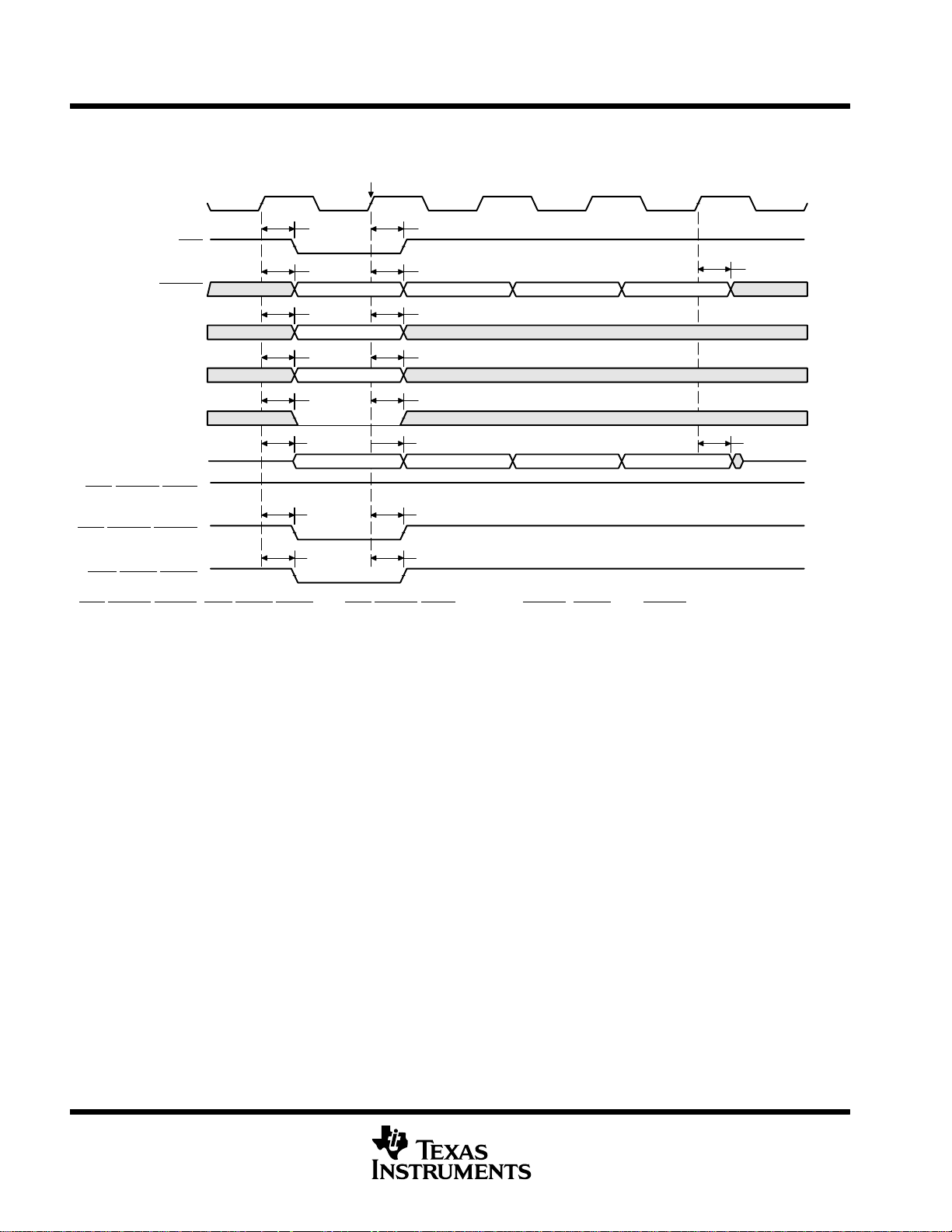
TMS320C6211, TMS320C6211B
FIXED-POINT DIGITAL SIGNAL PROCESSORS
SPRS073K − AUGUST 1998 − REVISED MARCH 2004
SYNCHRONOUS DRAM TIMING (CONTINUED)
WRITE
ECLKOUT
2
4
5
5
5
9
8
11
CEx
BE[3:0]
EA[21:13]
EA[11:2]
EA12
ED[31:0]
AOE/SDRAS/SSOE
ARE/SDCAS/SSADS
AWE/SDWE/SSWE
1
2
BE1 BE2 BE3 BE4
4
Bank
4
Column
4
9
D1 D2 D3 D4
†
8
†
11
†
3
10
†
ARE/SDCAS/SSADS, AWE/SDWE/SSWE, and AOE/SDRAS/SSOE operate as SDCAS, SDWE, and SDRAS, respectively, during SDRAM
accesses.
Figure 23. SDRAM Write Command
54
POST OFFICE BOX 1443 • HOUSTON, TEXAS 77251−1443

ECLKOUT
CEx
BE[3:0]
EA[21:13]
EA[11:2]
EA12
ED[31:0]
TMS320C6211, TMS320C6211B
FIXED-POINT DIGITAL SIGNAL PROCESSORS
SPRS073K − AUGUST 1998 − REVISED MARCH 2004
SYNCHRONOUS DRAM TIMING (CONTINUED)
ACTV
1
4
Bank Activate
4
Row Address
4
Row Address
1
5
5
5
/SDRAS/SSOE
AOE
ARE/SDCAS/SSADS
AWE/SDWE/SSWE
†
ARE/SDCAS/SSADS, AWE/SDWE/SSWE, and AOE/SDRAS/SSOE operate as SDCAS, SDWE, and SDRAS, respectively, during SDRAM
accesses.
†
†
†
12
12
Figure 24. SDRAM ACTV Command
DCAB
ECLKOUT
1
5
12
EA[21:13, 11:2]
/SDRAS/SSOE
AOE
1
CEx
BE[3:0]
4
EA12
ED[31:0]
12
†
ARE/SDCAS/SSADS
AWE/SDWE/SSWE
†
ARE/SDCAS/SSADS, AWE/SDWE/SSWE, and AOE/SDRAS/SSOE operate as SDCAS, SDWE, and SDRAS, respectively, during SDRAM
accesses.
†
11
†
11
Figure 25. SDRAM DCAB Command
POST OFFICE BOX 1443 • HOUSTON, TEXAS 77251−1443
55
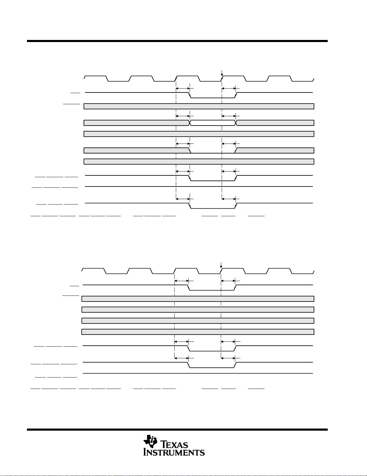
TMS320C6211, TMS320C6211B
FIXED-POINT DIGITAL SIGNAL PROCESSORS
SPRS073K − AUGUST 1998 − REVISED MARCH 2004
SYNCHRONOUS DRAM TIMING (CONTINUED)
DEAC
ECLKOUT
1
CEx
BE[3:0]
4
EA[21:13]
EA[11:2]
EA12
ED[31:0]
AOE/SDRAS/SSOE
ARE/SDCAS/SSADS
AWE/SDWE/SSWE
†
ARE/SDCAS/SSADS, AWE/SDWE/SSWE, and AOE/SDRAS/SSOE operate as SDCAS, SDWE, and SDRAS, respectively, during SDRAM
accesses.
†
†
†
Bank
4
12
11
1
5
5
12
11
Figure 26. SDRAM DEAC Command
REFR
ECLKOUT
1
CEx
BE[3:0]
EA[21:2]
EA12
ED[31:0]
/SDRAS/SSOE
AOE
ARE/SDCAS/SSADS
AWE/SDWE/SSWE
†
ARE/SDCAS/SSADS, AWE/SDWE/SSWE, and AOE/SDRAS/SSOE operate as SDCAS, SDWE, and SDRAS, respectively, during SDRAM
accesses.
†
†
†
12
8
1
12
8
Figure 27. SDRAM REFR Command
56
POST OFFICE BOX 1443 • HOUSTON, TEXAS 77251−1443
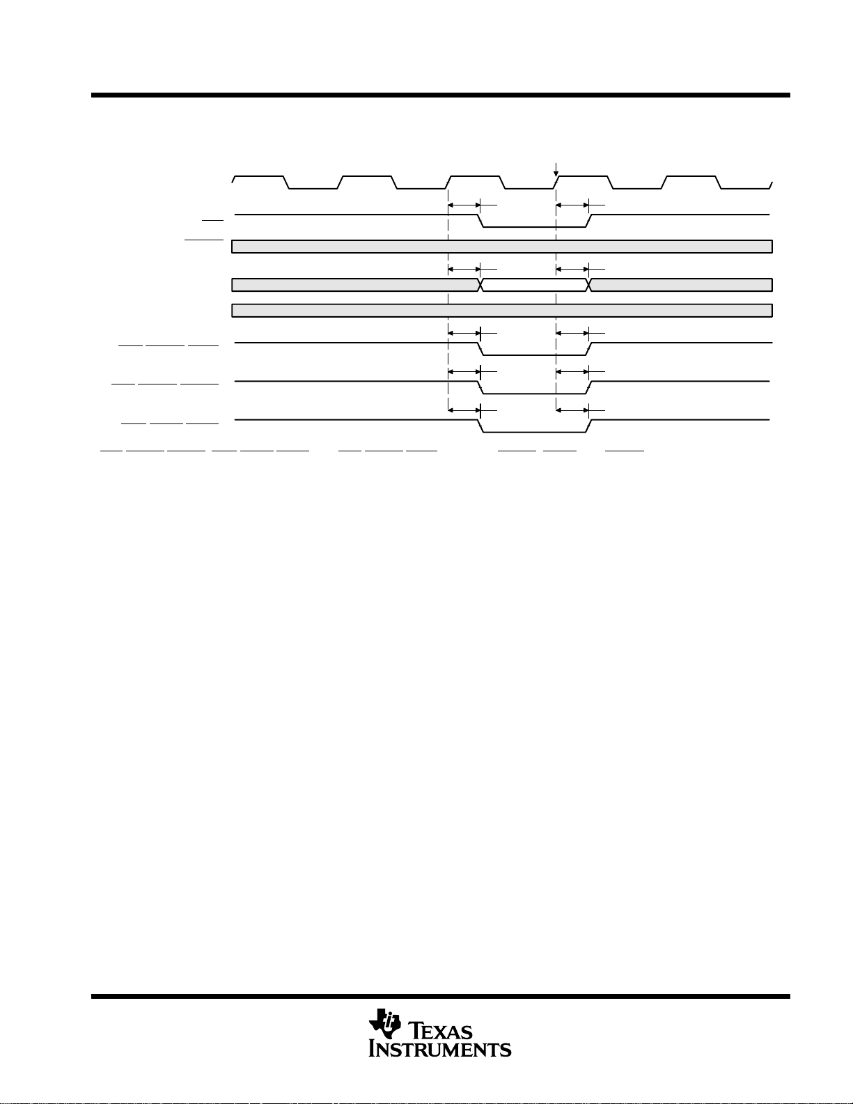
ECLKOUT
CEx
BE[3:0]
TMS320C6211, TMS320C6211B
FIXED-POINT DIGITAL SIGNAL PROCESSORS
SPRS073K − AUGUST 1998 − REVISED MARCH 2004
SYNCHRONOUS DRAM TIMING (CONTINUED)
MRS
1
1
4
EA[21:2]
ED[31:0]
AOE/SDRAS/SSOE
ARE/SDCAS/SSADS
AWE/SDWE/SSWE
†
ARE/SDCAS/SSADS, AWE/SDWE/SSWE, and AOE/SDRAS/SSOE operate as SDCAS, SDWE, and SDRAS, respectively, during SDRAM
accesses.
†
†
†
MRS value
12
8
11
5
12
8
11
Figure 28. SDRAM MRS Command
POST OFFICE BOX 1443 • HOUSTON, TEXAS 77251−1443
57

TMS320C6211, TMS320C6211B
NO
UNIT
NO
PARAMETER
UNIT
FIXED-POINT DIGITAL SIGNAL PROCESSORS
SPRS073K − AUGUST 1998 − REVISED MARCH 2004
HOLD/HOLDA TIMING
timing requirements for the HOLD
NO.
.
3 t
†
oh(HOLDAL-HOLDL)
E = ECLKIN period in ns
Output hold time, HOLD low after HOLDA low E ns
/HOLDA cycles† (see Figure 29)
−150
−167
MIN MAX
UNIT
switching characteristics over recommended operating conditions for the HOLD/HOLDA cycles
(see Figure 29)
−150
NO. PARAMETER
.
1 t
d(HOLDL-EMHZ)
2 t
d(EMHZ-HOLDAL)
4 t
d(HOLDH-EMLZ)
5 t
†
‡
§
d(EMLZ-HOLDAH)
E = ECLKIN period in ns
EMIF Bus consists of CE[3:0], BE[3:0], ED[31:0], EA[21:2], ARE/SDCAS/SSADS, AOE/SDRAS/SSOE, and AWE/SDWE/SSWE.
All pending EMIF transactions are allowed to complete before HOLDA is asserted. If no bus transactions are occurring, then the minimum delay
time can be achieved. Also, bus hold can be indefinitely delayed by setting NOHOLD = 1.
HOLD
Delay time, HOLD low to EMIF Bus high impedance 2E
Delay time, EMIF Bus high impedance to HOLDA low 0 2E ns
Delay time, HOLD high to EMIF Bus low impedance 2E 7E ns
Delay time, EMIF Bus low impedance to HOLDA high 0 2E ns
DSP Owns Bus
External Requestor
Owns Bus
3
DSP Owns Bus
−167
MIN MAX
UNIT
§
ns
†‡
HOLDA
EMIF Bus
†
EMIF Bus consists of CE[3:0], BE[3:0], ED[31:0], EA[21:2], ARE/SDCAS/SSADS, AOE/SDRAS/SSOE, and AWE/SDWE/SSWE.
†
C6211/C6211B C6211/C6211B
25
1
4
Figure 29. HOLD/HOLDA Timing
58
POST OFFICE BOX 1443 • HOUSTON, TEXAS 77251−1443

TMS320C6211, TMS320C6211B
NO
PARAMETER
UNIT
FIXED-POINT DIGITAL SIGNAL PROCESSORS
SPRS073K − AUGUST 1998 − REVISED MARCH 2004
BUSREQ TIMING
switching characteristics over recommended operating conditions for the BUSREQ cycles
(see Figure 30)
−150
.
NO. PARAMETER
1 t
d(EKOH-BUSRV)
ECLKOUT
Delay time, ECLKOUT high to BUSREQ valid 1.5 11 ns
−167
MIN MAX
UNIT
BUSREQ
1
Figure 30. BUSREQ Timing
1
POST OFFICE BOX 1443 • HOUSTON, TEXAS 77251−1443
59

TMS320C6211, TMS320C6211B
NO
UNIT
NO
PARAMETER
UNIT
FIXED-POINT DIGITAL SIGNAL PROCESSORS
SPRS073K − AUGUST 1998 − REVISED MARCH 2004
RESET TIMING
timing requirements for reset
†
(see Figure 31)
−150
NO.
.
−167
UNIT
MIN MAX
1 t
w(RST)
14 t
su(HD)
15 t
†
‡
§
h(HD)
P = 1/CPU clock frequency in ns. For example, when running parts at 167 MHz, use P = 6 ns.
This parameter applies to CLKMODE x1 when CLKIN is stable, and applies to CLKMODE x4 when CLKIN and PLL are stable.
This parameter applies to CLKMODE x4 only (it does not apply to CLKMODE x1). The RESET signal is not connected internally to the clock PLL
Width of the RESET pulse (PLL stable)
Width of the RESET pulse (PLL needs to sync up)
Setup time, HD boot configuration bits valid before RESET high
Hold time, HD boot configuration bits valid after RESET high
‡
§
¶
¶
10P ns
250 µs
2P ns
2P ns
circuit. The PLL, however, may need up to 250 µs to stabilize following device power up or after PLL configuration has been changed. During
that time, RESET
¶
HD[4:3] are the boot configuration pins during device reset.
switching characteristics over recommended operating conditions during reset
must be asserted to ensure proper device operation. See the clock PLL section for PLL lock times.
†#||
(see Figure 31)
−150
NO. PARAMETER
.
−167
UNIT
MIN MAX
2 t
d(RSTL-ECKI)
3 t
d(RSTH-ECKI)
4 t
d(RSTL-EMIFZHZ)
5 t
d(RSTH-EMIFZV)
6 t
d(RSTL-EMIFHIV)
7 t
d(RSTH-EMIFHV)
8 t
d(RSTL-EMIFLIV)
9 t
d(RSTH-EMIFLV)
10 t
d(RSTL-HIGHIV)
11 t
d(RSTH-HIGHV)
12 t
d(RSTL-ZHZ)
13 t
d(RSTH-ZV)
†
P = 1/CPU clock frequency in ns. For example, when running parts at 167 MHz, use P = 6 ns.
#
E = ECLKIN period in ns
||
EMIF Z group consists of: EA[21:2], ED[31:0], CE[3:0], BE[3:0], ARE/SDCAS/SSADS, AWE/SDWE/SSWE, and AOE/SDRAS/SSOE
Delay time, RESET low to ECLKIN synchronized internally 2P + 3E 3P + 4E ns
Delay time, RESET high to ECLKIN synchronized internally 2P + 3E 3P + 4E ns
Delay time, RESET low to EMIF Z group high impedance 2P + 3E ns
Delay time, RESET high to EMIF Z group valid 3P + 4E ns
Delay time, RESET low to EMIF high group invalid 2P + 3E ns
Delay time, RESET high to EMIF high group valid 3P + 4E ns
Delay time, RESET low to EMIF low group invalid 2P + 3E ns
Delay time, RESET high to EMIF low group valid 3P + 4E ns
Delay time, RESET low to high group invalid 2P ns
Delay time, RESET high to high group valid 4P ns
Delay time, RESET low to Z group high impedance 2P ns
Delay time, RESET high to Z group valid 2P ns
EMIF high group consists of: HOLDA
EMIF low group consists of: BUSREQ
High group consists of: HRDY
and HINT
Z group consists of: HD[15:0], CLKX0, CLKX1, FSX0, FSX1, DX0, DX1, CLKR0, CLKR1, FSR0, FSR1, TOUT0, and TOUT1.
60
POST OFFICE BOX 1443 • HOUSTON, TEXAS 77251−1443

CLKOUT1
CLKOUT2
TMS320C6211, TMS320C6211B
FIXED-POINT DIGITAL SIGNAL PROCESSORS
SPRS073K − AUGUST 1998 − REVISED MARCH 2004
RESET TIMING (CONTINUED)
1
14
15
RESET
ECLKIN
EMIF Z Group
EMIF High Group
§
†
†
32
54
76
98
EMIF Low Group
†
1110
High Group
†
1312
Z Group
HD[8, 4:3]
§
ECLKIN should be provided during reset in order to drive EMIF signals to the correct reset values. ECLKOUT continues to clock as long as
ECLKIN is provided.
†
EMIF Z group consists of: EA[21:2], ED[31:0], CE[3:0], BE[3:0], ARE/SDCAS/SSADS, AWE/SDWE/SSWE, and AOE/SDRAS/SSOE
†
‡
EMIF high group consists of: HOLDA
EMIF low group consists of: BUSREQ
High group consists of: HRDY
Z group consists of: HD[15:0], CLKX0, CLKX1, FSX0, FSX1, DX0, DX1, CLKR0, CLKR1, FSR0, FSR1, TOUT0, and TOUT1.
‡
HD[8, 4:3] are the endianness and boot configuration pins during device reset.
and HINT
Figure 31. Reset Timing
POST OFFICE BOX 1443 • HOUSTON, TEXAS 77251−1443
61

TMS320C6211, TMS320C6211B
NO
UNIT
FIXED-POINT DIGITAL SIGNAL PROCESSORS
SPRS073K − AUGUST 1998 − REVISED MARCH 2004
EXTERNAL INTERRUPT TIMING
timing requirements for external interrupts
NO.
.
1 t
w(ILOW)
2 t
†
w(IHIGH)
P = 1/CPU clock frequency in ns. For example, when running parts at 167 MHz, use P = 6 ns.
EXT_INT, NMI
Width of the interrupt pulse low 2P ns
Width of the interrupt pulse high 2P ns
†
(see Figure 32)
1
2
Figure 32. External/NMI Interrupt Timing
−150
−167
MIN MAX
UNIT
62
POST OFFICE BOX 1443 • HOUSTON, TEXAS 77251−1443

FIXED-POINT DIGITAL SIGNAL PROCESSORS
NO
UNIT
NO
PARAMETER
UNIT
SPRS073K − AUGUST 1998 − REVISED MARCH 2004
HOST-PORT INTERFACE TIMING
TMS320C6211, TMS320C6211B
timing requirements for host-port interface cycles [C6211]
†‡
(see Figure 33, Figure 34, Figure 35,
and Figure 36)
C6211−150
NO.
.
C6211−167
UNIT
MIN MAX
1 t
su(SELV-HSTBL)
2 t
h(HSTBL-SELV)
3 t
w(HSTBL)
4 t
w(HSTBH)
10 t
su(SELV-HASL)
11 t
h(HASL-SELV)
12 t
su(HDV-HSTBH)
13 t
h(HSTBH-HDV)
14 t
h(HRDYL-HSTBL)
18 t
su(HASL-HSTBL)
19 t
†
‡
§
h(HSTBL-HASL)
HSTROBE refers to the following logical operation on HCS, HDS1, and HDS2: [NOT(HDS1 XOR HDS2)] OR HCS.
P = 1/CPU clock frequency in ns. For example, when running parts at 167 MHz, use P = 6 ns.
Select signals include: HCNTL[1:0], HR/W, and HHWIL.
Setup time, select signals§ valid before HSTROBE low 5 ns
Hold time, select signals§ valid after HSTROBE low 4 ns
Pulse duration, HSTROBE low 4P ns
Pulse duration, HSTROBE high between consecutive accesses 4P ns
Setup time, select signals§ valid before HAS low 5 ns
Hold time, select signals§ valid after HAS low 3 ns
Setup time, host data valid before HSTROBE high 5 ns
Hold time, host data valid after HSTROBE high 3 ns
Hold time, HSTROBE low after HRDY low. HSTROBE should not be inactivated
until HRDY
is active (low); otherwise, HPI writes will not complete properly.
2 ns
Setup time, HAS low before HSTROBE low 2 ns
Hold time, HAS low after HSTROBE low 2 ns
switching characteristics over recommended operating conditions during host-port interface
cycles [C6211]
†‡
(see Figure 33, Figure 34, Figure 35, and Figure 36)
C6211−150
NO. PARAMETER
.
C6211−167
UNIT
MIN MAX
5 t
d(HCS-HRDY)
6 t
d(HSTBL-HRDYH)
7 t
d(HSTBL-HDLZ)
8 t
d(HDV-HRDYL)
9 t
oh(HSTBH-HDV)
15 t
d(HSTBH-HDHZ)
16 t
d(HSTBL-HDV)
17 t
d(HSTBH-HRDYH)
20 t
†
‡
¶
#
d(HASL-HRDYH)
HSTROBE refers to the following logical operation on HCS, HDS1, and HDS2: [NOT(HDS1 XOR HDS2)] OR HCS.
P = 1/CPU clock frequency in ns. For example, when running parts at 167 MHz, use P = 6 ns.
HCS enables HRDY, and HRDY is always low when HCS is high. The case where HRDY goes high when HCS falls indicates that HPI is busy
completing a previous HPID write or READ with autoincrement.
This parameter is used during an HPID read. At the beginning of the first half-word transfer on the falling edge of HSTROBE, the HPI sends the
Delay time, HCS to HRDY
Delay time, HSTROBE low to HRDY high
Delay time, HSTROBE low to HD low impedance for an HPI read 2 ns
Delay time, HD valid to HRDY low 2P − 4 2P ns
Output hold time, HD valid after HSTROBE high 3 15 ns
Delay time, HSTROBE high to HD high impedance 3 15 ns
Delay time, HSTROBE low to HD valid 3 15 ns
Delay time, HSTROBE high to HRDY high
Delay time, HAS low to HRDY high 3 15 ns
request to the EDMA internal address generation hardware, and HRDY
the requested data into HPID.
||
This parameter is used after the second half-word of an HPID write or autoincrement read. HRDY remains low if the access is not an HPID write
or autoincrement read. Reading or writing to HPIC or HPIA does not affect the HRDY
¶
#
||
1 15 ns
3 15 ns
3 15 ns
remains high until the EDMA internal address generation hardware loads
signal.
POST OFFICE BOX 1443 • HOUSTON, TEXAS 77251−1443
63

TMS320C6211, TMS320C6211B
NO
PARAMETER
UNIT
FIXED-POINT DIGITAL SIGNAL PROCESSORS
SPRS073K − AUGUST 1998 − REVISED MARCH 2004
HOST-PORT INTERFACE TIMING (CONTINUED)
timing requirements for host-port interface cycles [C6211BGFNA/C6211B]
Figure 34, Figure 35, and Figure 36)
NO.
1 t
2 t
3 t
4 t
10 t
11 t
12 t
13 t
su(SELV-HSTBL)
h(HSTBL-SELV)
w(HSTBL)
w(HSTBH)
su(SELV-HASL)
h(HASL-SELV)
su(HDV-HSTBH)
h(HSTBH-HDV)
Setup time, select signals§ valid before HSTROBE low 5 ns
Hold time, select signals§ valid after HSTROBE low 4 ns
Pulse duration, HSTROBE low 4P ns
Pulse duration, HSTROBE high between consecutive accesses 4P ns
Setup time, select signals§ valid before HAS low 5 ns
Hold time, select signals§ valid after HAS low 3 ns
Setup time, host data valid before HSTROBE high 5 ns
Hold time, host data valid after HSTROBE high 3 ns
Hold time, HSTROBE low after HRDY low. HSTROBE should not be
14 t
h(HRDYL-HSTBL)
inactivated until HRDY
is active (low); otherwise, HPI writes will not
complete properly.
18 t
su(HASL-HSTBL)
19 t
†
‡
§
h(HSTBL-HASL)
HSTROBE refers to the following logical operation on HCS, HDS1, and HDS2: [NOT(HDS1 XOR HDS2)] OR HCS.
P = 1/CPU clock frequency in ns. For example, when running parts at 167 MHz, use P = 6 ns.
Select signals include: HCNTL[1:0], HR/W, and HHWIL.
Setup time, HAS low before HSTROBE low 2 ns
Hold time, HAS low after HSTROBE low 2 ns
C6211BGFNA−150
MIN MAX
†‡
(see Figure 33,
C6211B−150
C6211B−167
UNIT
2 ns
switching characteristics over recommended operating conditions during host-port interface
cycles [C6211BGFNA/C6211B]
.
NO. PARAMETER
5 t
d(HCS-HRDY)
6 t
d(HSTBL-HRDYH)
7 t
d(HSTBL-HDLZ)
8 t
d(HDV-HRDYL)
9 t
oh(HSTBH-HDV)
15 t
d(HSTBH-HDHZ)
16 t
d(HSTBL-HDV)
17 t
d(HSTBH-HRDYH)
20 t
†
‡
¶
#
||
d(HASL-HRDYH)
HSTROBE refers to the following logical operation on HCS, HDS1, and HDS2: [NOT(HDS1 XOR HDS2)] OR HCS.
P = 1/CPU clock frequency in ns. For example, when running parts at 167 MHz, use P = 6 ns.
HCS enables HRDY, and HRDY is always low when HCS is high. The case where HRDY goes high when HCS falls indicates that HPI is busy
completing a previous HPID write or READ with autoincrement.
This parameter is used during an HPID read. At the beginning of the first half-word transfer on the falling edge of HSTROBE, the HPI sends the
request to the EDMA internal address generation hardware, and HRDY
the requested data into HPID.
This parameter is used after the second half-word of an HPID write or autoincrement read. HRDY remains low if the access is not an HPID write
or autoincrement read. Reading or writing to HPIC or HPIA does not affect the HRDY
†‡
(see Figure 33, Figure 34, Figure 35, and Figure 36)
C6211BGFNA−150
C6211B−150
C6211B−167
UNIT
MIN MAX MIN MAX
Delay time, HCS to HRDY
Delay time, HSTROBE low to HRDY high
Delay time, HSTROBE low to HD low impedance for
an HPI read
¶
#
1 13 1 12 ns
3 13 3 12 ns
2 2 ns
Delay time, HD valid to HRDY low 2P − 4 2P 2P − 4 2P ns
Output hold time, HD valid after HSTROBE high 3 13 3 12 ns
Delay time, HSTROBE high to HD high impedance 3 13 3 12 ns
Delay time, HSTROBE low to HD valid 3 13 3 12 ns
Delay time, HSTROBE high to HRDY high
||
3 13 3 12 ns
Delay time, HAS low to HRDY high 3 13 3 12 ns
remains high until the EDMA internal address generation hardware loads
signal.
64
POST OFFICE BOX 1443 • HOUSTON, TEXAS 77251−1443
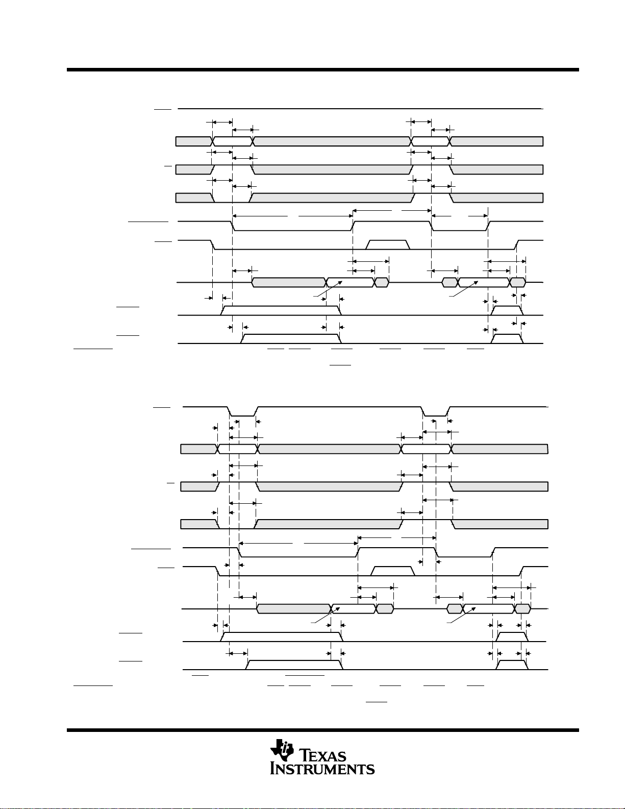
TMS320C6211, TMS320C6211B
FIXED-POINT DIGITAL SIGNAL PROCESSORS
SPRS073K − AUGUST 1998 − REVISED MARCH 2004
HOST-PORT INTERFACE TIMING (CONTINUED)
HAS
HCNTL[1:0]
HR/W
HHWIL
HSTROBE
HD[15:0] (output)
HRDY
HRDY
†
HSTROBE refers to the following logical operation on HCS, HDS1, and HDS2: [NOT(HDS1 XOR HDS2)] OR HCS.
†
HCS
(case 1)
(case 2)
1
1
1
2
2
2
3
15
97
1st halfword 2nd halfword
85
86
1
1
1
4
2
2
2
3
Figure 33. HPI Read Timing (HAS Not Used, Tied High)
†
HAS
10
HCNTL[1:0]
10
HR/W
10
HHWIL
HSTROBE
HD[15:0] (output)
HRDY (case 1)
HRDY
†
For correct operation, strobe the HAS signal only once per HSTROBE active cycle.
‡
HSTROBE refers to the following logical operation on HCS, HDS1, and HDS2: [NOT(HDS1 XOR HDS2)] OR HCS.
‡
HCS
(case 2)
19
1011
11
11
3
18
97
1st half-word 2nd half-word
10
10
4
15
19
11
11
11
18
15
17
17
916
5
5
15
916
51785
517820
Figure 34. HPI Read Timing (HAS Used)
POST OFFICE BOX 1443 • HOUSTON, TEXAS 77251−1443
65

TMS320C6211, TMS320C6211B
FIXED-POINT DIGITAL SIGNAL PROCESSORS
SPRS073K − AUGUST 1998 − REVISED MARCH 2004
HOST-PORT INTERFACE TIMING (CONTINUED)
HAS
HCNTL[1:0]
HR/W
HHWIL
HSTROBE
HD[15:0] (input)
†
HSTROBE refers to the following logical operation on HCS, HDS1, and HDS2: [NOT(HDS1 XOR HDS2)] OR HCS.
†
HCS
HRDY
1
2
1
1
5
2
2
3
14
12
1st halfword 2nd halfword
1
1
1
4
13
2
2
2
3
12
Figure 35. HPI Write Timing (HAS Not Used, Tied High)
†
HAS
19
11
10
HCNTL[1:0]
19
10
17
13
5
11
10
HR/W
10
HHWIL
HSTROBE
HD[15:0] (input)
†
For correct operation, strobe the HAS signal only once per HSTROBE active cycle.
‡
HSTROBE refers to the following logical operation on HCS, HDS1, and HDS2: [NOT(HDS1 XOR HDS2)] OR HCS.
‡
HCS
5
HRDY
11
11
3
14
18
12
1st half-word 2nd half-word
10
10
4
18
13
12
Figure 36. HPI Write Timing (HAS Used)
11
11
13
17
5
66
POST OFFICE BOX 1443 • HOUSTON, TEXAS 77251−1443

TMS320C6211, TMS320C6211B
NO
UNIT
FIXED-POINT DIGITAL SIGNAL PROCESSORS
SPRS073K − AUGUST 1998 − REVISED MARCH 2004
MULTICHANNEL BUFFERED SERIAL PORT TIMING
timing requirements for McBSP
†‡
(see Figure 37)
−150
NO.
.
−167
UNIT
MIN MAX
2 t
c(CKRX)
3 t
w(CKRX)
5 t
su(FRH-CKRL)
6 t
h(CKRL-FRH)
7 t
su(DRV-CKRL)
8 t
h(CKRL-DRV)
10 t
su(FXH-CKXL)
11 t
h(CKXL-FXH)
†
CLKRP = CLKXP = FSRP = FSXP = 0. If polarity of any of the signals is inverted, then the timing references of that signal are also inverted.
‡
P = 1/CPU clock frequency in ns. For example, when running parts at 167 MHz, use P = 6 ns.
§
The minimum CLKR/X period is twice the CPU cycle time (2P). This means that the maximum bit rate for communications between the McBSP
Cycle time, CLKR/X CLKR/X ext 2P
Pulse duration, CLKR/X high or CLKR/X low CLKR/X ext 0.5t
Setup time, external FSR high before CLKR low
Hold time, external FSR high after CLKR low
Setup time, DR valid before CLKR low
Hold time, DR valid after CLKR low
Setup time, external FSX high before CLKX low
Hold time, external FSX high after CLKX low
CLKR int 20
CLKR ext
CLKR int 6
CLKR ext
CLKR int 22
CLKR ext
CLKR int 3
CLKR ext
CLKX int 23
CLKX ext
CLKX int 6
CLKX ext 3
c(CKRX)
§
− 1 ns
1
3
3
4
1
and other device is 83 Mbps for 167 MHz CPU clock or 75 Mbps for 150 MHz CPU clock; where the McBSP is either the master or the slave.
Care must be taken to ensure that the AC timings specified in this data sheet are met. The maximum bit rate for McBSP-to-McBSP
communications is 33 Mbps; therefore, the minimum CLKR/X clock cycle is either twice the CPU cycle time (2P), or 30 ns (33 MHz), whichever
value is larger. For example, when running parts at 167 MHz (P = 6 ns), use 30 ns as the minimum CLKR/X clock cycle (by setting the appropriate
CLKGDV ratio or external clock source). When running parts at 60 MHz (P = 16.67 ns), use 2P = 33 ns (30 MHz) as the minimum CLKR/X clock
cycle. The maximum bit rate for McBSP-to-McBSP communications applies when the serial port is a master of the clock and frame syncs (with
CLKR connected to CLKX, FSR connected to FSX, CLKXM = FSXM = 1, and CLKRM = FSRM = 0) in data delay 1 or 2 mode (R/XDATDLY =
01b or 10b) and the other device the McBSP communicates to is a slave.
ns
ns
ns
ns
ns
ns
ns
POST OFFICE BOX 1443 • HOUSTON, TEXAS 77251−1443
67
TMS320C6211, TMS320C6211B
NO
PARAMETER
UNIT
Disable time, DX high impedance following last data bit
FIXED-POINT DIGITAL SIGNAL PROCESSORS
SPRS073K − AUGUST 1998 − REVISED MARCH 2004
MULTICHANNEL BUFFERED SERIAL PORT TIMING (CONTINUED)
switching characteristics over recommended operating conditions for McBSP
†‡
(see Figure 37)
−150
NO. PARAMETER
.
−167
UNIT
MIN MAX
1 t
d(CKSH-CKRXH)
2 t
c(CKRX)
3 t
w(CKRX)
4 t
d(CKRH-FRV)
9 t
d(CKXH-FXV)
12 t
dis(CKXH-DXHZ)
13 t
d(CKXH-DXV)
14 t
d(FXH-DXV)
†
CLKRP = CLKXP = FSRP = FSXP = 0. If polarity of any of the signals is inverted, then the timing references of that signal are also inverted.
‡
Minimum delay times also represent minimum output hold times.
§
P = 1/CPU clock frequency in ns. For example, when running parts at 167 MHz, use P = 6 ns.
¶
The minimum CLKR/X period is twice the CPU cycle time (2P). This means that the maximum bit rate for communications between the McBSP
Delay time, CLKS high to CLKR/X high for internal CLKR/X generated from
CLKS input
Cycle time, CLKR/X CLKR/X int 2P
Pulse duration, CLKR/X high or CLKR/X low CLKR/X int C − 1
4 26 ns
§¶
#
C + 1
#
ns
ns
Delay time, CLKR high to internal FSR valid CLKR int −11 3 ns
Delay time, CLKX high to internal FSX valid
Disable time, DX high impedance following last data bit
from CLKX high
Delay time, CLKX high to DX valid
Delay time, FSX high to DX valid
ONLY applies when in data
delay 0 (XDATDLY = 00b) mode
CLKX int −11 3
CLKX ext
3 9
CLKX int −9 4
CLKX ext
3 9
CLKX int −9+ D1||4 + D2
CLKX ext
3 + D1||19 + D2
FSX int −1 3
FSX ext 3 9
ns
ns
||
ns
||
ns
and other device is 83 Mbps for 167 MHz CPU clock or 75 Mbps for 150 MHz CPU clock; where the McBSP is either the master or the slave.
Care must be taken to ensure that the AC timings specified in this data sheet are met. The maximum bit rate for McBSP-to-McBSP
communications is 33 Mbps; therefore, the minimum CLKR/X clock cycle is either twice the CPU cycle time (2P), or 30 ns (33 MHz), whichever
value is larger. For example, when running parts at 167 MHz (P = 6 ns), use 30 ns as the minimum CLKR/X clock cycle (by setting the appropriate
CLKGDV ratio or external clock source). When running parts at 60 MHz (P = 16.67 ns), use 2P = 33 ns (30 MHz) as the minimum CLKR/X clock
cycle. The maximum bit rate for McBSP-to-McBSP communications applies when the serial port is a master of the clock and frame syncs (with
CLKR connected to CLKX, FSR connected to FSX, CLKXM = FSXM = 1, and CLKRM = FSRM = 0) in data delay 1 or 2 mode (R/XDATDLY =
01b or 10b) and the other device the McBSP communicates to is a slave.
#
C = H or L
S = sample rate generator input clock = 2P if CLKSM = 1 (P = 1/CPU clock frequency)
= sample rate generator input clock = P_clks if CLKSM = 0 (P_clks = CLKS period)
H = CLKX high pulse width = (CLKGDV/2 + 1) * S if CLKGDV is even
= (CLKGDV + 1)/2 * S if CLKGDV is odd or zero
L = CLKX low pulse width = (CLKGDV/2) * S if CLKGDV is even
= (CLKGDV + 1)/2 * S if CLKGDV is odd or zero
CLKGDV should be set appropriately to ensure the McBSP bit rate does not exceed the maximum limit (see ¶ footnote above).
||
Extra delay from CLKX high to DX valid applies only to the first data bit of a device, if and only if DXENA = 1 in SPCR.
If DXENA = 0, then D1 = D2 = 0
If DXENA = 1, then D1 = 2P, D2 = 4P
68
POST OFFICE BOX 1443 • HOUSTON, TEXAS 77251−1443

TMS320C6211, TMS320C6211B
FIXED-POINT DIGITAL SIGNAL PROCESSORS
SPRS073K − AUGUST 1998 − REVISED MARCH 2004
MULTICHANNEL BUFFERED SERIAL PORT TIMING (CONTINUED)
CLKS
1
CLKR
4
FSR (int)
5
FSR (ext)
DR
CLKX
9
FSX (int)
10
FSX (ext)
2
3
3
4
6
7
Bit(n-1) (n-2) (n-3)
2
3
3
11
8
FSX (XDATDLY=00b)
DX
14
1312
Bit 0 Bit(n-1) (n-2) (n-3)
13
Figure 37. McBSP Timings
POST OFFICE BOX 1443 • HOUSTON, TEXAS 77251−1443
69

TMS320C6211, TMS320C6211B
NO
UNIT
FIXED-POINT DIGITAL SIGNAL PROCESSORS
SPRS073K − AUGUST 1998 − REVISED MARCH 2004
MULTICHANNEL BUFFERED SERIAL PORT TIMING (CONTINUED)
timing requirements for FSR when GSYNC = 1 (see Figure 38)
NO.
.
1 t
su(FRH-CKSH)
2 t
h(CKSH-FRH)
CLKR/X (no need to resync)
CLKR/X (needs resync)
Setup time, FSR high before CLKS high 4 ns
Hold time, FSR high after CLKS high 4 ns
CLKS
1
FSR external
2
Figure 38. FSR Timing When GSYNC = 1
−150
−167
MIN MAX
UNIT
70
POST OFFICE BOX 1443 • HOUSTON, TEXAS 77251−1443
TMS320C6211, TMS320C6211B
FIXED-POINT DIGITAL SIGNAL PROCESSORS
SPRS073K − AUGUST 1998 − REVISED MARCH 2004
MULTICHANNEL BUFFERED SERIAL PORT TIMING (CONTINUED)
−150
−167
†‡
(see Figure 39)
UNIT
timing requirements for McBSP as SPI master or slave: CLKSTP = 10b, CLKXP = 0
NO.
4 t
su(DRV-CKXL)
5 t
†
‡
h(CKXL-DRV)
P = 1/CPU clock frequency in ns. For example, when running parts at 167 MHz, use P = 6 ns.
For all SPI slave modes, CLKG is programmed as 1/2 of the CPU clock by setting CLKSM = CLKGDV = 1.
Setup time, DR valid before CLKX low 26 2 − 6P ns
Hold time, DR valid after CLKX low 4 6 + 12P ns
MASTER SLAVE
MIN MAX MIN MAX
switching characteristics over recommended operating conditions for McBSP as SPI master or
slave: CLKSTP = 10b, CLKXP = 0
NO. PARAMETER
1 t
h(CKXL-FXL)
2 t
d(FXL-CKXH)
3 t
d(CKXH-DXV)
6 t
dis(CKXL-DXHZ)
7 t
dis(FXH-DXHZ)
8 t
†
‡
§
¶
#
d(FXL-DXV)
P = 1/CPU clock frequency in ns. For example, when running parts at 167 MHz, use P = 6 ns.
For all SPI slave modes, CLKG is programmed as 1/2 of the CPU clock by setting CLKSM = CLKGDV = 1.
S = Sample rate generator input clock = 2P if CLKSM = 1 (P = 1/CPU clock frequency)
= Sample rate generator input clock = P_clks if CLKSM = 0 (P_clks = CLKS period)
T = CLKX period = (1 + CLKGDV) * S
H = CLKX high pulse width = (CLKGDV/2 + 1) * S if CLKGDV is even
L = CLKX low pulse width = (CLKGDV/2) * S if CLKGDV is even
FSRP = FSXP = 1. As a SPI master, FSX is inverted to provide active-low slave-enable output. As a slave, the active-low signal input on FSX
and FSR is inverted before being used internally.
CLKXM = FSXM = 1, CLKRM = FSRM = 0 for master McBSP
CLKXM = CLKRM = FSXM = FSRM = 0 for slave McBSP
FSX should be low before the rising edge of clock to enable slave devices and then begin a SPI transfer at the rising edge of the master clock
(CLKX).
Hold time, FSX low after CLKX low
Delay time, FSX low to CLKX high
Delay time, CLKX high to DX valid −9 9 6P + 4 10P + 20 ns
Disable time, DX high impedance following last data bit from
CLKX low
Disable time, DX high impedance following last data bit from
FSX high
Delay time, FSX low to DX valid 4P + 2 8P + 20 ns
= (CLKGDV + 1)/2 * S if CLKGDV is odd or zero
= (CLKGDV + 1)/2 * S if CLKGDV is odd or zero
†‡
(see Figure 39)
¶
#
−150
−167
MASTER
MIN MAX MIN MAX
T − 9 T + 9 ns
L − 9 L + 9 ns
L − 9 L + 9 ns
§
SLAVE
2P + 3 6P + 20 ns
UNIT
POST OFFICE BOX 1443 • HOUSTON, TEXAS 77251−1443
71

TMS320C6211, TMS320C6211B
FIXED-POINT DIGITAL SIGNAL PROCESSORS
SPRS073K − AUGUST 1998 − REVISED MARCH 2004
MULTICHANNEL BUFFERED SERIAL PORT TIMING (CONTINUED)
CLKX
21
FSX
6
DX
DR
Bit 0 Bit(n-1) (n-2) (n-3) (n-4)
Bit 0 Bit(n-1) (n-2) (n-3) (n-4)
Figure 39. McBSP Timing as SPI Master or Slave: CLKSTP = 10b, CLKXP = 0
87
3
4
5
72
POST OFFICE BOX 1443 • HOUSTON, TEXAS 77251−1443
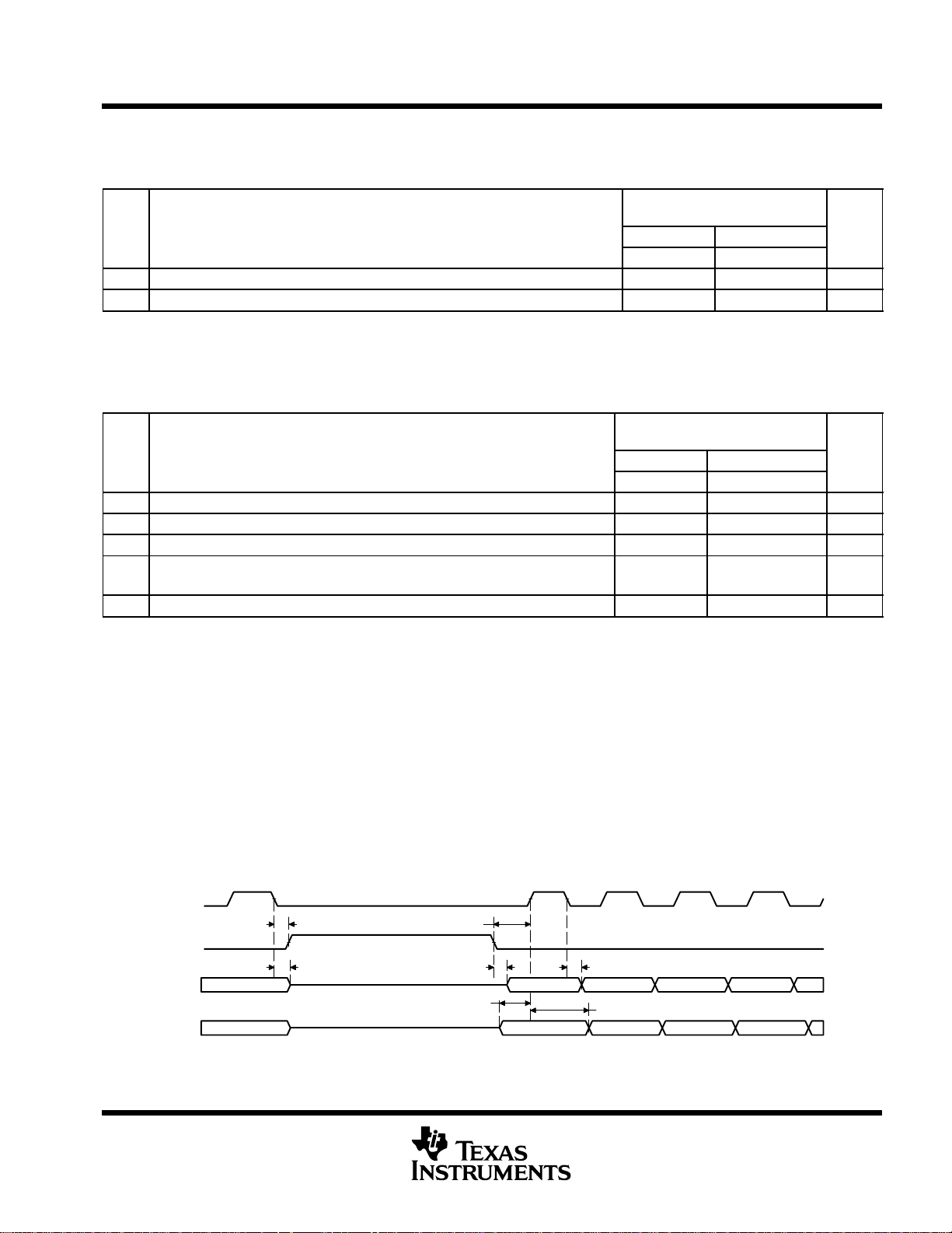
TMS320C6211, TMS320C6211B
FIXED-POINT DIGITAL SIGNAL PROCESSORS
SPRS073K − AUGUST 1998 − REVISED MARCH 2004
MULTICHANNEL BUFFERED SERIAL PORT TIMING (CONTINUED)
−150
−167
†‡
(see Figure 40)
UNIT
timing requirements for McBSP as SPI master or slave: CLKSTP = 11b, CLKXP = 0
NO.
4 t
su(DRV-CKXH)
5 t
†
‡
h(CKXH-DRV)
P = 1/CPU clock frequency in ns. For example, when running parts at 167 MHz, use P = 6 ns.
For all SPI slave modes, CLKG is programmed as 1/2 of the CPU clock by setting CLKSM = CLKGDV = 1.
Setup time, DR valid before CLKX high 26 2 − 6P ns
Hold time, DR valid after CLKX high 4 6 + 12P ns
MASTER SLAVE
MIN MAX MIN MAX
switching characteristics over recommended operating conditions for McBSP as SPI master or
slave: CLKSTP = 11b, CLKXP = 0
NO. PARAMETER
1 t
h(CKXL-FXL)
2 t
d(FXL-CKXH)
3 t
d(CKXL-DXV)
6 t
dis(CKXL-DXHZ)
7 t
†
‡
§
¶
#
d(FXL-DXV)
P = 1/CPU clock frequency in ns. For example, when running parts at 167 MHz, use P = 6 ns.
For all SPI slave modes, CLKG is programmed as 1/2 of the CPU clock by setting CLKSM = CLKGDV = 1.
S = Sample rate generator input clock = 2P if CLKSM = 1 (P = 1/CPU clock frequency)
= Sample rate generator input clock = P_clks if CLKSM = 0 (P_clks = CLKS period)
T = CLKX period = (1 + CLKGDV) * S
H = CLKX high pulse width = (CLKGDV/2 + 1) * S if CLKGDV is even
L = CLKX low pulse width = (CLKGDV/2) * S if CLKGDV is even
FSRP = FSXP = 1. As a SPI master, FSX is inverted to provide active-low slave-enable output. As a slave, the active-low signal input on FSX
and FSR is inverted before being used internally.
CLKXM = FSXM = 1, CLKRM = FSRM = 0 for master McBSP
CLKXM = CLKRM = FSXM = FSRM = 0 for slave McBSP
FSX should be low before the rising edge of clock to enable slave devices and then begin a SPI transfer at the rising edge of the master clock
(CLKX).
Hold time, FSX low after CLKX low
Delay time, FSX low to CLKX high
Delay time, CLKX low to DX valid −9 9 6P + 4 10P + 20 ns
Disable time, DX high impedance following last data bit from
CLKX low
Delay time, FSX low to DX valid H − 9 H + 9 4P + 2 8P + 20 ns
= (CLKGDV + 1)/2 * S if CLKGDV is odd or zero
= (CLKGDV + 1)/2 * S if CLKGDV is odd or zero
†‡
(see Figure 40)
¶
#
−150
−167
MASTER
MIN MAX MIN MAX
L − 9 L + 9 ns
T − 9 T + 9 ns
§
−9 9 6P + 3 10P + 20 ns
SLAVE
UNIT
CLKX
FSX
DX
DR
21
376
Bit 0 Bit(n-1) (n-2) (n-3) (n-4)
4
Bit 0 Bit(n-1) (n-2) (n-3) (n-4)
5
Figure 40. McBSP Timing as SPI Master or Slave: CLKSTP = 11b, CLKXP = 0
POST OFFICE BOX 1443 • HOUSTON, TEXAS 77251−1443
73

TMS320C6211, TMS320C6211B
FIXED-POINT DIGITAL SIGNAL PROCESSORS
SPRS073K − AUGUST 1998 − REVISED MARCH 2004
MULTICHANNEL BUFFERED SERIAL PORT TIMING (CONTINUED)
−150
−167
†‡
(see Figure 41)
UNIT
timing requirements for McBSP as SPI master or slave: CLKSTP = 10b, CLKXP = 1
NO.
4 t
su(DRV-CKXH)
5 t
†
‡
h(CKXH-DRV)
P = 1/CPU clock frequency in ns. For example, when running parts at 167 MHz, use P = 6 ns.
For all SPI slave modes, CLKG is programmed as 1/2 of the CPU clock by setting CLKSM = CLKGDV = 1.
Setup time, DR valid before CLKX high 26 2 − 6P ns
Hold time, DR valid after CLKX high 4 6 + 12P ns
MASTER SLAVE
MIN MAX MIN MAX
switching characteristics over recommended operating conditions for McBSP as SPI master or
slave: CLKSTP = 10b, CLKXP = 1
NO. PARAMETER
1 t
h(CKXH-FXL)
2 t
d(FXL-CKXL)
3 t
d(CKXL-DXV)
6 t
dis(CKXH-DXHZ)
7 t
dis(FXH-DXHZ)
8 t
†
‡
§
¶
#
d(FXL-DXV)
P = 1/CPU clock frequency in ns. For example, when running parts at 167 MHz, use P = 6 ns.
For all SPI slave modes, CLKG is programmed as 1/2 of the CPU clock by setting CLKSM = CLKGDV = 1.
S = Sample rate generator input clock = 2P if CLKSM = 1 (P = 1/CPU clock frequency)
= Sample rate generator input clock = P_clks if CLKSM = 0 (P_clks = CLKS period)
T = CLKX period = (1 + CLKGDV) * S
H = CLKX high pulse width = (CLKGDV/2 + 1) * S if CLKGDV is even
L = CLKX low pulse width = (CLKGDV/2) * S if CLKGDV is even
FSRP = FSXP = 1. As a SPI master, FSX is inverted to provide active-low slave-enable output. As a slave, the active-low signal input on FSX
and FSR is inverted before being used internally.
CLKXM = FSXM = 1, CLKRM = FSRM = 0 for master McBSP
CLKXM = CLKRM = FSXM = FSRM = 0 for slave McBSP
FSX should be low before the rising edge of clock to enable slave devices and then begin a SPI transfer at the rising edge of the master clock
(CLKX).
Hold time, FSX low after CLKX high
Delay time, FSX low to CLKX low
Delay time, CLKX low to DX valid −9 9 6P + 4 10P + 20 ns
Disable time, DX high impedance following last data bit from
CLKX high
Disable time, DX high impedance following last data bit from
FSX high
Delay time, FSX low to DX valid 4P + 2 8P + 20 ns
= (CLKGDV + 1)/2 * S if CLKGDV is odd or zero
= (CLKGDV + 1)/2 * S if CLKGDV is odd or zero
†‡
(see Figure 41)
#
−150
−167
MASTER
MIN MAX MIN MAX
¶
T − 9 T + 9 ns
H − 9 H + 9 ns
H − 9 H + 9 ns
§
SLAVE
2P + 3 6P + 20 ns
UNIT
74
POST OFFICE BOX 1443 • HOUSTON, TEXAS 77251−1443

CLKX
FSX
DX
DR
TMS320C6211, TMS320C6211B
FIXED-POINT DIGITAL SIGNAL PROCESSORS
SPRS073K − AUGUST 1998 − REVISED MARCH 2004
MULTICHANNEL BUFFERED SERIAL PORT TIMING (CONTINUED)
21
6
7
Bit 0 Bit(n-1) (n-2) (n-3) (n-4)
4
Bit 0 Bit(n-1) (n-2) (n-3) (n-4)
Figure 41. McBSP Timing as SPI Master or Slave: CLKSTP = 10b, CLKXP = 1
38
5
POST OFFICE BOX 1443 • HOUSTON, TEXAS 77251−1443
75

TMS320C6211, TMS320C6211B
FIXED-POINT DIGITAL SIGNAL PROCESSORS
SPRS073K − AUGUST 1998 − REVISED MARCH 2004
MULTICHANNEL BUFFERED SERIAL PORT TIMING (CONTINUED)
−150
−167
†‡
(see Figure 42)
UNIT
timing requirements for McBSP as SPI master or slave: CLKSTP = 11b, CLKXP = 1
NO.
4 t
su(DRV-CKXH)
5 t
†
‡
h(CKXH-DRV)
P = 1/CPU clock frequency in ns. For example, when running parts at 167 MHz, use P = 6 ns.
For all SPI slave modes, CLKG is programmed as 1/2 of the CPU clock by setting CLKSM = CLKGDV = 1.
Setup time, DR valid before CLKX high 26 2 − 6P ns
Hold time, DR valid after CLKX high 4 6 + 12P ns
MASTER SLAVE
MIN MAX MIN MAX
switching characteristics over recommended operating conditions for McBSP as SPI master or
slave: CLKSTP = 11b, CLKXP = 1
NO. PARAMETER
1 t
h(CKXH-FXL)
2 t
d(FXL-CKXL)
3 t
d(CKXH-DXV)
6 t
dis(CKXH-DXHZ)
7 t
†
‡
§
¶
#
d(FXL-DXV)
P = 1/CPU clock frequency in ns. For example, when running parts at 167 MHz, use P = 6 ns.
For all SPI slave modes, CLKG is programmed as 1/2 of the CPU clock by setting CLKSM = CLKGDV = 1.
S = Sample rate generator input clock = 2P if CLKSM = 1 (P = 1/CPU clock frequency)
= Sample rate generator input clock = P_clks if CLKSM = 0 (P_clks = CLKS period)
T = CLKX period = (1 + CLKGDV) * S
H = CLKX high pulse width = (CLKGDV/2 + 1) * S if CLKGDV is even
L = CLKX low pulse width = (CLKGDV/2) * S if CLKGDV is even
FSRP = FSXP = 1. As a SPI master, FSX is inverted to provide active-low slave-enable output. As a slave, the active-low signal input on FSX
and FSR is inverted before being used internally.
CLKXM = FSXM = 1, CLKRM = FSRM = 0 for master McBSP
CLKXM = CLKRM = FSXM = FSRM = 0 for slave McBSP
FSX should be low before the rising edge of clock to enable slave devices and then begin a SPI transfer at the rising edge of the master clock
(CLKX).
Hold time, FSX low after CLKX high
Delay time, FSX low to CLKX low
Delay time, CLKX high to DX valid −9 9 6P + 4 10P + 20 ns
Disable time, DX high impedance following last data bit from
CLKX high
Delay time, FSX low to DX valid L − 9 L + 9 4P + 2 8P + 20 ns
= (CLKGDV + 1)/2 * S if CLKGDV is odd or zero
= (CLKGDV + 1)/2 * S if CLKGDV is odd or zero
†‡
(see Figure 42)
#
−150
−167
MASTER
MIN MAX MIN MAX
¶
H − 9 H + 9 ns
T − 9 T + 9 ns
§
−9 9 6P + 3 10P + 20 ns
SLAVE
UNIT
76
POST OFFICE BOX 1443 • HOUSTON, TEXAS 77251−1443

TMS320C6211, TMS320C6211B
FIXED-POINT DIGITAL SIGNAL PROCESSORS
SPRS073K − AUGUST 1998 − REVISED MARCH 2004
MULTICHANNEL BUFFERED SERIAL PORT TIMING (CONTINUED)
CLKX
21
FSX
7
4
DX
DR
6
Bit 0 Bit(n-1) (n-2) (n-3) (n-4)
Bit 0 Bit(n-1) (n-2) (n-3) (n-4)
Figure 42. McBSP Timing as SPI Master or Slave: CLKSTP = 11b, CLKXP = 1
3
5
POST OFFICE BOX 1443 • HOUSTON, TEXAS 77251−1443
77

TMS320C6211, TMS320C6211B
NO
UNIT
NO
PARAMETER
UNIT
FIXED-POINT DIGITAL SIGNAL PROCESSORS
SPRS073K − AUGUST 1998 − REVISED MARCH 2004
TIMER TIMING
timing requirements for timer inputs
NO.
.
1 t
w(TINPH)
2 t
†
w(TINPL)
P = 1/CPU clock frequency in ns. For example, when running parts at 167 MHz, use P = 6 ns.
Pulse duration, TINP high 2P ns
Pulse duration, TINP low 2P ns
†
(see Figure 43)
−150
−167
MIN MAX
switching characteristics over recommended operating conditions for timer outputs
(see Figure 43)
−150
NO. PARAMETER
.
3 t
w(TOUTH)
4 t
†
w(TOUTL)
P = 1/CPU clock frequency in ns. For example, when running parts at 167 MHz, use P = 6 ns.
TINPx
TOUTx
Pulse duration, TOUT high 4P−3 ns
Pulse duration, TOUT low 4P−3 ns
2
1
3
Figure 43. Timer Timing
4
−167
MIN MAX
UNIT
†
UNIT
78
POST OFFICE BOX 1443 • HOUSTON, TEXAS 77251−1443

TMS320C6211, TMS320C6211B
NO
UNIT
NO
PARAMETER
UNIT
FIXED-POINT DIGITAL SIGNAL PROCESSORS
SPRS073K − AUGUST 1998 − REVISED MARCH 2004
JTAG TEST-PORT TIMING
timing requirements for JTAG test port (see Figure 44)
−150
NO.
.
1 t
3 t
4 t
c(TCK)
su(TDIV-TCKH)
h(TCKH-TDIV)
Cycle time, TCK 35 ns
Setup time, TDI/TMS/TRST valid before TCK high 10 ns
Hold time, TDI/TMS/TRST valid after TCK high 9 ns
switching characteristics over recommended operating conditions for JTAG test port
(see Figure 44)
NO. PARAMETER
.
2 t
d(TCKL-TDOV)
Delay time, TCK low to TDO valid –3 18 ns
−167
MIN MAX
−150
−167
MIN MAX
UNIT
UNIT
TCK
TDO
TDI/TMS/TRST
1
2
3
Figure 44. JTAG Test-Port Timing
2
4
POST OFFICE BOX 1443 • HOUSTON, TEXAS 77251−1443
79
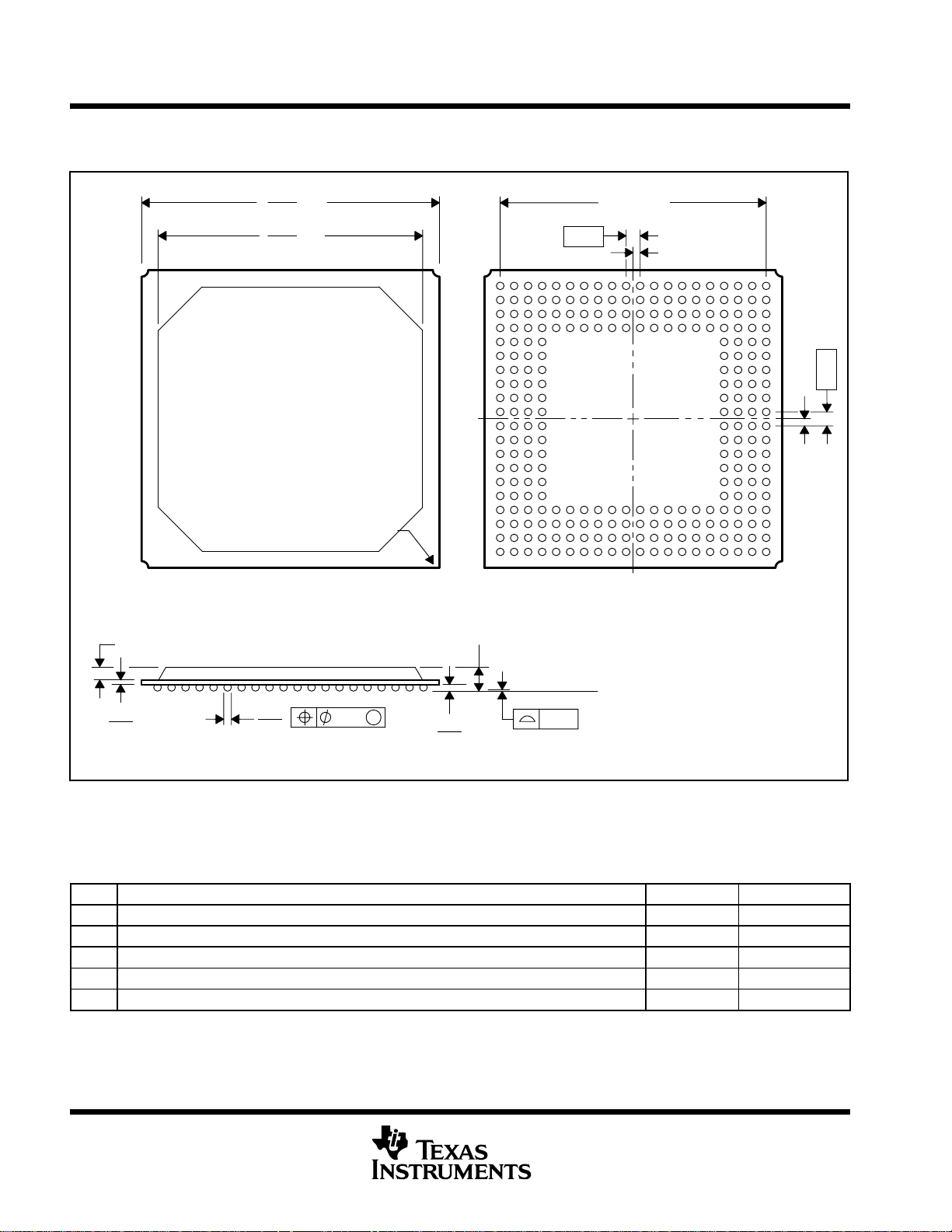
TMS320C6211, TMS320C6211B
FIXED-POINT DIGITAL SIGNAL PROCESSORS
SPRS073K − AUGUST 1998 − REVISED MARCH 2004
MECHANICAL DATA
GFN (S-PBGA-N256) PLASTIC BALL GRID ARRAY
1,17 NOM
27,20
26,80
24,70
23,80
SQ
SQ
A1 Corner
Y
W
V
U
T
R
P
N
M
L
K
J
H
G
F
E
D
C
B
A
2,32 MAX
24,13 TYP
1,27
0,635
1,27
0,635
31
75
10 12 14 16 18 208642
Bottom View
1915 1713119
Seating Plane
0,40
0,30
NOTES: A. All linear dimensions are in millimeters.
B. This drawing is subject to change without notice.
C. Falls within JEDEC MO-151
0,90
0,60
0,15
M
0,70
0,50
0,15
4040185-2/D 02/02
thermal resistance characteristics (S-PBGA package)
NO °C/W Air Flow (m/s)
1 RΘ
2 RΘ
3 RΘ
4 RΘ
5 RΘ
†
m/s = meters per second
Junction-to-case 6.4 N/A
JC
Junction-to-free air 25.5 0.0
JA
Junction-to-free air 23.1 0.5
JA
Junction-to-free air 22.3 1.0
JA
Junction-to-free air 21.2 2.0
JA
†
80
POST OFFICE BOX 1443 • HOUSTON, TEXAS 77251−1443

TMS320C6211, TMS320C6211B
FIXED-POINT DIGITAL SIGNAL PROCESSORS
SPRS073K − AUGUST 1998 − REVISED MARCH 2004
REVISION HISTORY
This data sheet revision history highlights the technical changes made to the SPRS073J device-specific data
sheet to make it an SPRS073K revision.
Scope: Applicable updates to the C62x device family, specifically relating to the C6211 and C6211B devices,
have been incorporated.
PAGE(S)
NO.
35 Power-down mode logic section:
Updated the text found under Figure 8.
ADDITIONS/CHANGES/DELETIONS
POST OFFICE BOX 1443 • HOUSTON, TEXAS 77251−1443
81
PACKAGE OPTION ADDENDUM
www.ti.com
17-Dec-2004
PACKAGING INFORMATION
Orderable Device Status
(1)
Package
Type
Package
Drawing
Pins Package
Qty
Eco Plan
TMS320C6211BGFN150 ACTIVE BGA GFN 256 40 None SNPB Level-4-220C-72HR
TMS320C6211BGFN167 ACTIVE BGA GFN 256 40 None SNPB Level-4-220C-72HR
TMS320C6211GFN150 NRND BGA GFN 256 None Call TI Call TI
TMS320C6211GFN167 NRND BGA GFN 256 None Call TI Call TI
TMS32C6211BGFNA150 ACTIVE BGA GFN 256 40 None SNPB Level-4-220C-72HR
TMX320C6211GFN OBSOLETE BGA GFN 256 None Call TI Call TI
TMX320C6211GFN21 OBSOLETE BGA GFN 256 None Call TI Call TI
(1)
The marketing status values are defined as follows:
ACTIVE: Product device recommended for new designs.
LIFEBUY: TI has announced that the device will be discontinued, and a lifetime-buy period is in effect.
NRND: Not recommended for new designs. Device is in production to support existing customers, but TI does not recommend using this part in
a new design.
PREVIEW: Device has been announced but is not in production. Samples may or may not be available.
OBSOLETE: TI has discontinued the production of the device.
(2)
Eco Plan - May not be currently available - please check http://www.ti.com/productcontent for the latest availability information and additional
product content details.
None: Not yet available Lead (Pb-Free).
Pb-Free (RoHS): TI's terms "Lead-Free" or "Pb-Free" mean semiconductor products that are compatible with the current RoHS requirements
for all 6 substances, including the requirement that lead not exceed 0.1% by weight in homogeneous materials. Where designed to be soldered
at high temperatures, TI Pb-Free products are suitable for use in specified lead-free processes.
Green (RoHS & no Sb/Br): TI defines "Green" to mean "Pb-Free" and in addition, uses package materials that do not contain halogens,
including bromine (Br) or antimony (Sb) above 0.1% of total product weight.
(2)
Lead/Ball Finish MSL Peak Temp
(3)
(3)
MSL, Peak Temp. -- The Moisture Sensitivity Level rating according to the JEDECindustry standard classifications, and peak solder
temperature.
Important Information and Disclaimer:The information provided on this page represents TI's knowledge and belief as of the date that it is
provided. TI bases its knowledge and belief on information provided by third parties, and makes no representation or warranty as to the
accuracy of such information. Efforts are underway to better integrate information from third parties. TI has taken and continues to take
reasonable steps to provide representative and accurate information but may not have conducted destructive testing or chemical analysis on
incoming materials and chemicals. TI and TI suppliers consider certain information to be proprietary, and thus CAS numbers and other limited
information may not be available for release.
In no event shall TI's liability arising out of such information exceed the total purchase price of the TI part(s) at issue in this document sold by TI
to Customer on an annual basis.
Addendum-Page 1

IMPORTANT NOTICE
Texas Instruments Incorporated and its subsidiaries (TI) reserve the right to make corrections, modifications,
enhancements, improvements, and other changes to its products and services at any time and to discontinue
any product or service without notice. Customers should obtain the latest relevant information before placing
orders and should verify that such information is current and complete. All products are sold subject to TI’s terms
and conditions of sale supplied at the time of order acknowledgment.
TI warrants performance of its hardware products to the specifications applicable at the time of sale in
accordance with TI’s standard warranty. Testing and other quality control techniques are used to the extent TI
deems necessary to support this warranty . Except where mandated by government requirements, testing of all
parameters of each product is not necessarily performed.
TI assumes no liability for applications assistance or customer product design. Customers are responsible for
their products and applications using TI components. To minimize the risks associated with customer products
and applications, customers should provide adequate design and operating safeguards.
TI does not warrant or represent that any license, either express or implied, is granted under any TI patent right,
copyright, mask work right, or other TI intellectual property right relating to any combination, machine, or process
in which TI products or services are used. Information published by TI regarding third-party products or services
does not constitute a license from TI to use such products or services or a warranty or endorsement thereof.
Use of such information may require a license from a third party under the patents or other intellectual property
of the third party, or a license from TI under the patents or other intellectual property of TI.
Reproduction of information in TI data books or data sheets is permissible only if reproduction is without
alteration and is accompanied by all associated warranties, conditions, limitations, and notices. Reproduction
of this information with alteration is an unfair and deceptive business practice. TI is not responsible or liable for
such altered documentation.
Resale of TI products or services with statements different from or beyond the parameters stated by TI for that
product or service voids all express and any implied warranties for the associated TI product or service and
is an unfair and deceptive business practice. TI is not responsible or liable for any such statements.
Following are URLs where you can obtain information on other Texas Instruments products and application
solutions:
Products Applications
Amplifiers amplifier.ti.com Audio www.ti.com/audio
Data Converters dataconverter.ti.com Automotive www.ti.com/automotive
DSP dsp.ti.com Broadband www.ti.com/broadband
Interface interface.ti.com Digital Control www.ti.com/digitalcontrol
Logic logic.ti.com Military www.ti.com/military
Power Mgmt power.ti.com Optical Networking www.ti.com/opticalnetwork
Microcontrollers microcontroller.ti.com Security www.ti.com/security
Telephony www.ti.com/telephony
Video & Imaging www.ti.com/video
Wireless www.ti.com/wireless
Mailing Address: Texas Instruments
Post Office Box 655303 Dallas, Texas 75265
Copyright 2004, Texas Instruments Incorporated
 Loading...