

Texas Instruments TMX320C6201BGJL, TMS320C6201GGP200, TMS320C6201GGP167, TMS320C6201GJLA200, TMS320C6201GJL200 Datasheet
...
TMS320C6201, TMS320C6201B
DIGITAL SIGNAL PROCESSORS
SPRS051F – JANUARY 1997 – REVISED AUGUST 1999
1
POST OFFICE BOX 1443 • HOUSTON, TEXAS 77251–1443
D
Highest Performance Fixed-Point Digital
Signal Processor (DSP) TMS320C6201
– 6-, 5-ns Instruction Cycle Time
– 167-, 200-MHz Clock Rate
– Eight 32-Bit Instructions/Cycle
– 1336, 1600 MIPS
D
Highest Performance Fixed-Point Digital
Signal Processor (DSP) TMS320C6201B
– 5-, 4.3-ns Instruction Cycle Time
– 200-, and 233-MHz Clock Rates
– Eight 32-Bit Instructions/Cycle
– 1600, 1860 MIPS
D
VelociTI Advanced Very Long Instruction
Word (VLIW) ’C62x CPU Core
– Eight Independent Functional Units:
– Six ALUs (32-/40-Bit)
– Two 16-Bit Multipliers (32-Bit Results)
– Load-Store Architecture With 32 32-Bit
General-Purpose Registers
– Instruction Packing Reduces Code Size
– All Instructions Conditional
D
Instruction Set Features
– Byte-Addressable (8-, 16-, 32-Bit Data)
– 32-Bit Address Range
– 8-Bit Overflow Protection
– Saturation
– Bit-Field Extract, Set, Clear
– Bit-Counting
– Normalization
D
1M-Bit On-Chip SRAM
– 512K-Bit Internal Program/Cache
(16K 32-Bit Instructions)
– 512K-Bit Dual-Access Internal Data
(64K Bytes) Organized as a Single Block
(’6201)
– 512K-Bit Dual-Access Internal Data
(64K Bytes) Organized as Two Blocks for
Improved Concurrency (’6201B)
D
32-Bit External Memory Interface (EMIF)
– Glueless Interface to Synchronous
Memories: SDRAM and SBSRAM
– Glueless Interface to Asynchronous
Memories: SRAM and EPROM
D
Four-Channel Bootloading
Direct-Memory-Access (DMA) Controller
with an Auxiliary Channel
D
16-Bit Host-Port Interface (HPI)
– Access to Entire Memory Map
D
Two Multichannel Buffered Serial Ports
(McBSPs)
– Direct Interface to T1/E1, MVIP, SCSA
Framers
– ST-Bus-Switching Compatible
– Up to 256 Channels Each
– AC97-Compatible
– Serial Peripheral Interface (SPI)
Compatible (Motorola)
D
Two 32-Bit General-Purpose Timers
D
Flexible Phase-Locked Loop (PLL) Clock
Generator
D
IEEE-1149.1 (JTAG†) Boundary-Scan
Compatible
D
352-Pin BGA Package (GGP Suffix) (’6201)
D
352-Pin BGA Package (GJC Suffix) (’6201B)
D
352-Pin BGA Package (GJL Suffix) (’6201B)
D
CMOS T echnology
– 0.25-µm/5-Level Metal Process (’6201)
– 0.18-µm/5-Level Metal Process (’6201B)
D
3.3-V I/Os, 2.5-V Internal (’6201)
D
3.3-V I/Os, 1.8-V Internal (’6201B)
Please be aware that an important notice concerning availability, standard warranty, and use in critical applications of
Texas Instruments semiconductor products and disclaimers thereto appears at the end of this data sheet.
VelociTI is a trademark of Texas Instruments Incorporated.
Motorola is a trademark of Motorola, Inc.
†
IEEE Standard 1149.1-1990 Standard-Test-Access Port and Boundary Scan Architecture.
Copyright 1999, Texas Instruments Incorporated
UNLESS OTHERWISE NOTED this document contains PRODUCTION
DATA information current as of publication date. Products conform to
specifications per the terms of Texas Instruments standard warranty.
Production processing does not necessarily include testing of all
parameters.
GJC/GJL/GGP
352-PIN BALL GRID ARRAY (BGA) PACKAGES
(BOTTOM VIEW)
AF
AD
AB
AA
AC
W
Y
U
V
AE
R
N
P
L
H
J
K
M
F
G
D
E
B
A
C
T
25
26222320
19 211715
16121314 181098756432
111
24
TMS320C6201, TMS320C6201B
DIGITAL SIGNAL PROCESSORS
SPRS051F – JANUARY 1997 – REVISED AUGUST 1999
2
POST OFFICE BOX 1443 • HOUSTON, TEXAS 77251–1443
description
The TMS320C62x† DSPs (including the TMS320C6201 and the TMS320C6201B devices) are the fixed-point
DSP family in the TMS320C6000 platform. The TMS320C6201 (’C6201) and the TMS320C6201B (’C6201B)
devices are based on the high-performance, advanced VelociTI very-long-instruction-word (VLIW) architecture
developed by Texas Instruments (TI), making these DSPs an excellent choice for multichannel and
multifunction applications. With performance of up to 1600 million instructions per second (MIPS) at a clock rate
of 200 MHz, the ’C6201 offers cost-effective solutions to high-performance DSP programming challenges. The
’C6201B is a newer revision of the ’C6201 with performance of up to 1860 MIPS at a clock rate of 233 MHz.
The ’C6201/’C6201B DSPs possess the operational flexibility of high-speed controllers and the numerical
capability of array processors. Each of these processors have 32 general-purpose registers of 32-bit word
length and eight highly independent functional units. The eight functional units provide six arithmetic logic units
(ALUs) for a high degree of parallelism and two 16-bit multipliers for a 32-bit result. Both the ’C6201 and the
’C6201B can produce two multiply-accumulates (MACs) per cycle—for a total of 400 million MACs per second
(MMACS) for the ’C6201, and a total of 466 MMACS for the ’C6201B. The ’C62x DSP also has
application-specific hardware logic, on-chip memory, and additional on-chip peripherals.
The ’C6201/’C6201B includes a large bank of on-chip memory and has a powerful and diverse set of
peripherals. Program memory consists of a 64K-byte block that is user-configurable as cache or
memory-mapped program space. Data memory of the ’C6201 consists of a 64K-byte block of RAM, while data
memory of the ’C6201B consists of two 32K-byte blocks of RAM for improved concurrency . The peripheral set
includes two multichannel buffered serial ports (McBSPs), two general-purpose timers, a host-port interface
(HPI), and a glueless external memory interface (EMIF) capable of interfacing to SDRAM or SBSRAM and
asynchronous peripherals.
The ’C62x has a complete set of development tools which includes: a new C compiler, an assembly optimizer
to simplify programming and scheduling, and a Windows debugger interface for visibility into source code
execution.
device characteristics
Table 1 provides an overview of the ’C62x DSP. The table shows significant features of each device, including
the capacity of on-chip RAM, the peripherals, the execution time, and the package type with pin count.
Table 1. Characteristics of the ’C6201/’C6201B Processors
CHARACTERISTICS DESCRIPTION
Device Number TMS320C6201 TMS320C6201B
On-Chip Memory
512-Kbit Program Memory
512-Kbit Data Memory (organized as a single block)
512-Kbit Program Memory
512-Kbit Data Memory (organized as two blocks)
Peripherals
2 Multichannel Buffered Serial Ports (McBSPs)
2 General-Purpose Timers
Host-Port Interface (HPI)
External Memory Interface (EMIF)
2 Multichannel Buffered Serial Ports (McBSPs)
2 General-Purpose Timers
Host-Port Interface (HPI)
External Memory Interface (EMIF)
Cycle Time
5 ns (TMS320C6201-200),
6 ns (TMS320C6201-167)
4.3 ns (TMS320C6201B-233),
5 ns (TMS320C6201B-200)
Package Type 35 mm × 35 mm, 352-Pin BGA (GGP)
35 mm × 35 mm, 352-Pin BGA (GJC),
27 mm × 27 mm, 352-Pin BGA (GJL)
Nominal Voltage
2.5 V Core
3.3 V I/O
1.8 V Core
3.3 V I/O
TI is a trademark of Texas Instruments Incorporated.
Windows is a registered trademark of the Microsoft Corporation.
†
Where unique device characteristics are specified, TMS320C6201 and TMS320C6201B identifiers are used. For generic characteristics, no
identifiers are needed, ’C62x is used, or ’C6000 is used.
TMS320C6201, TMS320C6201B
DIGITAL SIGNAL PROCESSORS
SPRS051F – JANUARY 1997 – REVISED AUGUST 1999
3
POST OFFICE BOX 1443 • HOUSTON, TEXAS 77251–1443
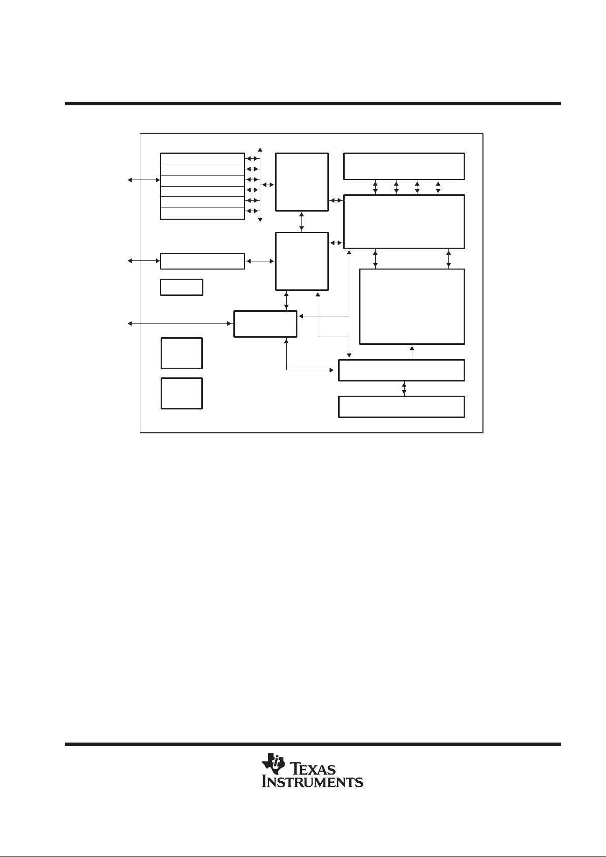
functional block diagram
EMIF
Timers
Interrupt Selector
McBSPs
HPI Control
DMA Control
EMIF Control
Host-Port Interface
PLL
Power
Down
Boot-
Config.
Peripheral
Bus
Controller
DMA
Controller
Data Memory
Data Memory
Controller
CPU
Program Memory Controller
Program Memory/Cache

TMS320C6201, TMS320C6201B
DIGITAL SIGNAL PROCESSORS
SPRS051F – JANUARY 1997 – REVISED AUGUST 1999
4
POST OFFICE BOX 1443 • HOUSTON, TEXAS 77251–1443
CPU description
The CPU fetches VelociTI advanced very-long instruction words (VLIW) (256 bits wide) to supply up to eight
32-bit instructions to the eight functional units during every clock cycle. The VelociTI VLIW architecture features
controls by which all eight units do not have to be supplied with instructions if they are not ready to execute. The
first bit of every 32-bit instruction determines if the next instruction belongs to the same execute packet as the
previous instruction, or whether it should be executed in the following clock as a part of the next execute packet.
Fetch packets are always 256 bits wide; however, the execute packets can vary in size. The variable-length
execute packets are a key memory-saving feature, distinguishing the ’C62x CPU from other VLIW architectures.
The CPU features two sets of functional units. Each set contains four units and a register file. One set contains
functional units .L1, .S1, .M1, and .D1; the other set contains units .D2, .M2, .S2, and .L2. The two register files
each contain 16 32-bit registers for a total of 32 general-purpose registers. The two sets of functional units, along
with two register files, compose sides A and B of the CPU (see Figure 1 and Figure 2). The four functional units
on each side of the CPU can freely share the 16 registers belonging to that side. Additionally , each side features
a single data bus connected to all the registers on the other side, by which the two sets of functional units can
access data from the register files on the opposite side. While register access by functional units on the same
side of the CPU as the register file can service all the units in a single clock cycle, register access using the
register file across the CPU supports one read and one write per cycle.
Another key feature of the ’C62x CPU is the load/store architecture, where all instructions operate on registers
(as opposed to data in memory). Two sets of data-addressing units (.D1 and .D2) are responsible for all data
transfers between the register files and the memory. The data address driven by the .D units allows data
addresses generated from one register file to be used to load or store data to or from the other register file. The
’C62x CPU supports a variety of indirect addressing modes using either linear- or circular-addressing modes
with 5- or 15-bit offsets. All instructions are conditional, and most can access any one of the 32 registers. Some
registers, however, are singled out to support specific addressing or to hold the condition for conditional
instructions (if the condition is not automatically “true”). The two .M functional units are dedicated for multiplies.
The two .S and .L functional units perform a general set of arithmetic, logical, and branch functions with results
available every clock cycle.
The processing flow begins when a 256-bit-wide instruction fetch packet is fetched from a program memory.
The 32-bit instructions destined for the individual functional units are “linked” together by “1” bits in the least
significant bit (LSB) position of the instructions. The instructions that are “chained” together for simultaneous
execution (up to eight in total) compose an execute packet. A “0” in the LSB of an instruction breaks the chain,
effectively placing the instructions that follow it in the next execute packet. If an execute packet crosses the fetch
packet boundary (256 bits wide), the assembler places it in the next fetch packet, while the remainder of the
current fetch packet is padded with NOP instructions. The number of execute packets within a fetch packet can
vary from one to eight. Execute packets are dispatched to their respective functional units at the rate of one per
clock cycle and the next 256-bit fetch packet is not fetched until all the execute packets from the current fetch
packet have been dispatched. After decoding, the instructions simultaneously drive all active functional units
for a maximum execution rate of eight instructions every clock cycle. While most results are stored in 32-bit
registers, they can be subsequently moved to memory as bytes or half-words as well. All load and store
instructions are byte-, half-word, or word-addressable.
TMS320C6201, TMS320C6201B
DIGITAL SIGNAL PROCESSORS
SPRS051F – JANUARY 1997 – REVISED AUGUST 1999
5
POST OFFICE BOX 1443 • HOUSTON, TEXAS 77251–1443
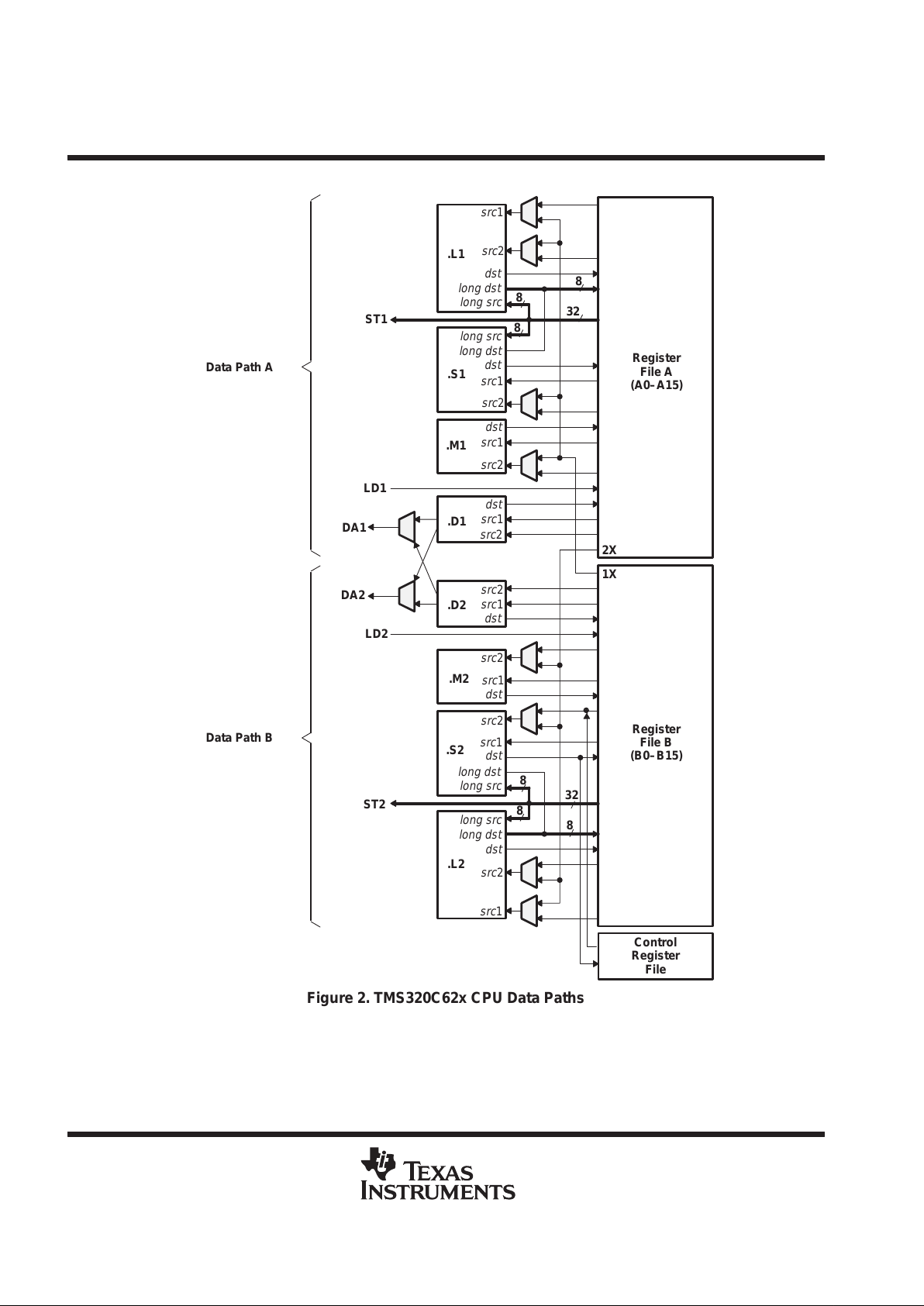
CPU description (continued)
Á
Á
’C62x CPU
Program Memory
32-Bit Address
256-Bit Data
External Memory
Interface
Data Memory
32-Bit Address
8-, 16-, 32-Bit Data
Program Fetch
Instruction Dispatch
Instruction Decode
Data Path A
Register File A
Data Path B
Register File B
.L1 .S1 .M1 .D1 .D2
.M2
.S2 .L2
Control
Registers
Control
Logic
Test
Emulation
Interrupts
Additional
Peripherals:
Timers,
Serial Ports,
etc.
Figure 1. TMS320C62x CPU Block Diagram
TMS320C6201, TMS320C6201B
DIGITAL SIGNAL PROCESSORS
SPRS051F – JANUARY 1997 – REVISED AUGUST 1999
6
POST OFFICE BOX 1443 • HOUSTON, TEXAS 77251–1443
CPU description (continued)
2X
1X
.L2
.S2
.M2
.D2
.D1
.M1
.S1
.L1
long src
dst
src
2
src
1
src
1
src
1
src
1
src
1
src
1
src
1
src
1
8
8
8
8
8
8
long dst
long dst
dst
dst
dst
dst
dst
dst
dst
src
2
src
2
src
2
src
2
src
2
src
2
src
2
long src
DA1
DA2
ST1
LD1
LD2
ST2
32
32
Register
File A
(A0–A15)
long src
long dst
long dst
long src
Data Path B
Data Path A
Register
File B
(B0–B15)
Control
Register
File
Figure 2. TMS320C62x CPU Data Paths
TMS320C6201, TMS320C6201B
DIGITAL SIGNAL PROCESSORS
SPRS051F – JANUARY 1997 – REVISED AUGUST 1999
7
POST OFFICE BOX 1443 • HOUSTON, TEXAS 77251–1443
signal groups description
HHWIL
HBE0
HBE1
HCNTL0
HCNTL1
TRST
EXT_INT7
Clock/PLL
JTAG
Emulation
Reserved
Data
Register Select
Half-Word/Byte
Select
Boot Mode
Reset and
Interrupts
Little ENDIAN
Big ENDIAN
DMA Status
Power-Down
Status
Control
HPI
(Host-Port Interface)
16
Control/Status
TDI
TDO
TMS
TCK
CLKIN
CLKOUT2
CLKOUT1
CLKMODE1
CLKMODE0
PLLFREQ3
PLLFREQ2
PLLFREQ1
PLLV
PLLG
PLLF
EMU1
EMU0
RSV3
RSV2
RSV1
RSV0
HD[15:0]
BOOTMODE4
BOOTMODE3
BOOTMODE2
BOOTMODE1
BOOTMODE0
NMI
IACK
INUM3
INUM2
INUM1
INUM0
LENDIAN
DMAC3
DMAC2
DMAC1
DMAC0
PD
HAS
HR/W
HCS
HDS1
HDS2
HRDY
HINT
RSV7
RSV6
RSV5
RSV4
RSV8
EXT_INT6
EXT_INT5
EXT_INT4
RESET
RSV9
Figure 3. CPU and Peripheral Signals
TMS320C6201, TMS320C6201B
DIGITAL SIGNAL PROCESSORS
SPRS051F – JANUARY 1997 – REVISED AUGUST 1999
8
POST OFFICE BOX 1443 • HOUSTON, TEXAS 77251–1443
signal groups description (continued)
CE3
ARE
ED[31:0]
CE2
CE1
CE0
EA[21:2]
BE3
BE2
BE1
BE0
HOLD
HOLDA
TOUT1
CLKX1
FSX1
DX1
CLKR1
FSR1
DR1
CLKS1
AOE
AWE
ARDY
SSADS
SSOE
SSWE
SSCLK
SDA10
SDRAS
SDCAS
SDWE
SDCLK
TOUT0
CLKX0
FSX0
DX0
CLKR0
FSR0
DR0
CLKS0
Data
Memory Map
Space Select
Word Address
Byte Enables
HOLD/
HOLDA
32
20
Asynchronous
Memory
Control
SBSRAM
Control
SDRAM
Control
EMIF
(External Memory Interface)
Timer 1
Receive Receive
Timer 0
Timers
McBSP1 McBSP0
Transmit Transmit
Clock Clock
McBSPs
(Multichannel Buffered Serial Ports)
TINP1
TINP0
Figure 4. Peripheral Signals
TMS320C6201, TMS320C6201B
DIGITAL SIGNAL PROCESSORS
SPRS051F – JANUARY 1997 – REVISED AUGUST 1999
9
POST OFFICE BOX 1443 • HOUSTON, TEXAS 77251–1443
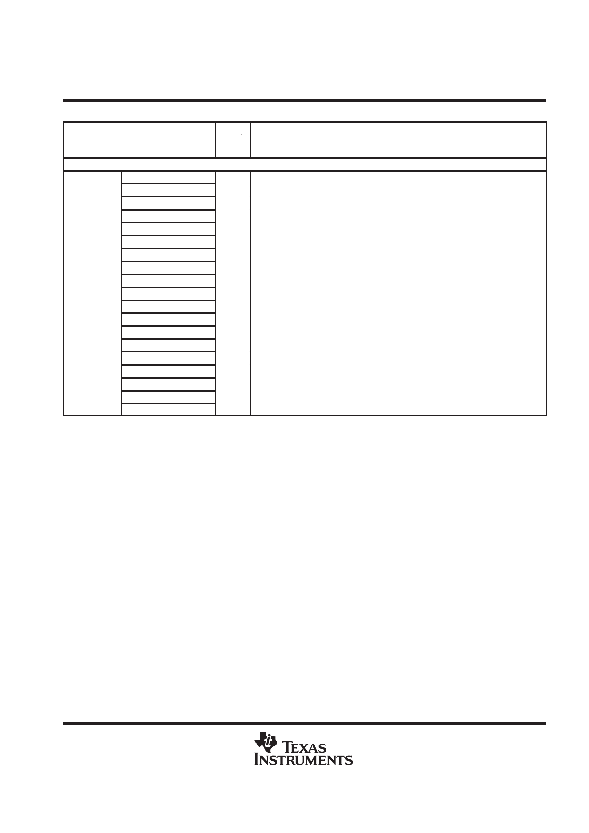
Signal Descriptions
SIGNAL
NAME
GGP, GJC
PIN NO.
GJL
PIN NO.
TYPE
†
DESCRIPTION
CLOCK/PLL
CLKIN C10 B9 I Clock Input
CLKOUT1 AF22 AC18 O Clock output at full device speed
CLKOUT2 AF20 AC16 O Clock output at half of device speed
CLKMODE1 C6 D8
Clock-mode select
CLKMODE0 C5 C7
I
• Selects whether the CPU clock frequency = input clock frequency x4 or x1
PLLFREQ3 A9 A9 PLL frequency range (3, 2, and 1)
PLLFREQ2 D11 D11
I
• The target range for CLKOUT1 frequency is determined by the 3-bit value of the
PLLFREQ pins.
PLLFREQ1 B10 B10
PLLV
‡
D12 B11 A
§
PLL analog VCC connection for the low-pass filter
PLLG
‡
C12 C12 A
§
PLL analog GND connection for the low-pass filter
PLLF A11 D12 A
§
PLL low-pass filter connection to external components and a bypass capacitor
JTAG EMULATION
TMS L3 L3 I JTAG test port mode select (features an internal pullup)
TDO W2 U4 O/Z JTAG test port data out
TDI R4 T2 I JTAG test port data in (features an internal pullup)
TCK R3 R3 I JTAG test port clock
TRST T1 R4 I JTAG test port reset (features an internal pulldown)
EMU1 Y1 V3 I/O/Z Emulation pin 1, pullup with a dedicated 20-kΩ resistor
¶
EMU0 W3 W2 I/O/Z Emulation pin 0, pullup with a dedicated 20-kΩ resistor
¶
RESET AND INTERRUPTS
RESET K2 K2 I Device reset
NMI L2 L2 I
Nonmaskable interrupt
• Edge-driven (rising edge)
EXT_INT7 U3 U2
EXT_INT6 V2 T4
External interrupts
EXT_INT5 W1 V1
I
• Edge-driven (rising edge)
EXT_INT4 U4 V2
IACK Y2 Y1 O Interrupt acknowledge for all active interrupts serviced by the CPU
INUM3 AA1 V4
INUM2 W4 Y2
Active interrupt identification number
p
INUM1 AA2 AA1
O
•Va
lid duri
ng
IACK f
or all active interrupts (not just externa
l)
• Encoding order follows the interrupt-service fetch-packet orderin
g
INUM0 AB1 W4
• Encoding order follows the interru t service fetch acket ordering
LITTLE ENDIAN/BIG ENDIAN
LENDIAN H3 G2 I
If high, LENDIAN selects little-endian byte/half-word addressing order within a word
If low, LENDIAN selects big-endian addressing
POWER-DOWN STATUS
PD D3 E2 O Power-down mode 2 or 3 (active if high)
†
I = Input, O = Output, Z = High Impedance, S = Supply Voltage, GND = Ground
‡
PLLV and PLLG are not part of external voltage supply or ground. See the
clock PLL
section for information on how to connect these pins.
§
A = Analog Signal (PLL Filter)
¶
For emulation and normal operation, pull up EMU1 and EMU0 with a dedicated 20-kΩ resistor. For boundary scan, pull down EMU1 and EMU0
with a dedicated 20-kΩ resistor.
TMS320C6201, TMS320C6201B
DIGITAL SIGNAL PROCESSORS
SPRS051F – JANUARY 1997 – REVISED AUGUST 1999
10
POST OFFICE BOX 1443 • HOUSTON, TEXAS 77251–1443
Signal Descriptions (Continued)
SIGNAL
NAME
GGP, GJC
PIN NO.
GJL
PIN NO.
TYPE
†
DESCRIPTION
HOST-PORT INTERFACE (HPI)
HINT H26 J26 O Host interrupt (from DSP to host)
HCNTL1 F23 G24 I Host control – selects between control, address, or data registers
HCNTL0 D25 F25 I Host control – selects between control, address, or data registers
HHWIL C26 E26 I Host half-word select – first or second half-word (not necessarily high or low order)
HBE1 E23 F24 I Host byte select within word or half-word
HBE0 D24 E25 I Host byte select within word or half-word
HR/W C23 B22 I Host read or write select
HD15 B13 A12
HD14 B14 D13
HD13 C14 C13
HD12 B15 D14
HD11 D15 B15
HD10 B16 C15
HD9 A17 D15
HD8 B17 B16
p
HD7 D16 C16
I/O/Z
Host-port data (used for transfer of data, address, and control)
HD6 B18 B17
HD5 A19 D16
HD4 C18 A18
HD3 B19 B18
HD2 C19 D17
HD1 B20 C18
HD0 B21 A20
HAS C22 C20 I Host address strobe
HCS B23 B21 I Host chip select
HDS1 D22 C21 I Host data strobe 1
HDS2 A24 D20 I Host data strobe 2
HRDY J24 J25 O Host ready (from DSP to host)
BOOT MODE
BOOTMODE4 D8 C8
BOOTMODE3 B4 B6
BOOTMODE2 A3 D7
I Boot mode
BOOTMODE1 D5 C6
BOOTMODE0 C4 B5
†
I = Input, O = Output, Z = High Impedance, S = Supply Voltage, GND = Ground

TMS320C6201, TMS320C6201B
DIGITAL SIGNAL PROCESSORS
SPRS051F – JANUARY 1997 – REVISED AUGUST 1999
11
POST OFFICE BOX 1443 • HOUSTON, TEXAS 77251–1443
Signal Descriptions (Continued)
SIGNAL
NAME
GGP, GJC
PIN NO.
GJL
PIN NO.
TYPE
†
DESCRIPTION
EMIF – CONTROL SIGNALS COMMON TO ALL TYPES OF MEMORY
CE3 AE22 AD20
CE2 AD26 AA24
Memory space enables
CE1 AB24 AB26
O/Z
• Enabled by bits 24 and 25 of the word address
CE0 AC26 AA25 • Only one asserted during any external data access
BE3 AB25 Y24 Byte-enable control
BE2 AA24 W23
• Decoded from the two lowest bits of the internal address
BE1 Y23 AA26
O/Z
• Byte-write enables for most types of memory
BE0 AA26 W25 • Can be directly connected to SDRAM read and write mask signal (SDQM)
EMIF – ADDRESS
EA21 J26 K25
EA20 K25 L24
EA19 L24 L25
EA18 K26 M23
EA17 M26 M25
EA16 M25 M24
EA15 P25 N23
EA14 P24 P24
EA13 R25 P23
EA12 T26 R25
EA11 R23 R24
O/Z
External address (word address)
EA10 U26 R23
EA9 U25 T25
EA8 T23 T24
EA7 V26 U25
EA6 V25 T23
EA5 W26 V26
EA4 V24 V25
EA3 W25 U23
EA2 Y26 V24
†
I = Input, O = Output, Z = High Impedance, S = Supply Voltage, GND = Ground
TMS320C6201, TMS320C6201B
DIGITAL SIGNAL PROCESSORS
SPRS051F – JANUARY 1997 – REVISED AUGUST 1999
12
POST OFFICE BOX 1443 • HOUSTON, TEXAS 77251–1443
Signal Descriptions (Continued)
SIGNAL
NAME
GGP, GJC
PIN NO.
GJL
PIN NO.
TYPE
†
DESCRIPTION
EMIF – DATA
ED31 AB2 Y3
ED30 AC1 AA2
ED29 AA4 AB1
ED28 AD1 AA3
ED27 AC3 AB2
ED26 AD4 AE5
ED25 AF3 AD6
ED24 AE4 AC7
ED23 AD5 AE6
ED22 AF4 AD7
ED21 AE5 AC8
ED20 AD6 AD8
ED19 AE6 AC9
ED18 AD7 AF7
ED17 AC8 AD9
ED16 AF7 AC10
ED15 AD9 AE9
I/O/Z
External data
ED14 AD10 AF9
ED13 AF9 AC11
ED12 AC11 AE10
ED11 AE10 AD11
ED10 AE11 AE11
ED9 AF11 AC12
ED8 AE14 AD12
ED7 AF15 AE12
ED6 AE15 AC13
ED5 AF16 AD14
ED4 AC15 AC14
ED3 AE17 AE15
ED2 AF18 AD15
ED1 AF19 AE16
ED0 AC17 AD16
EMIF – ASYNCHRONOUS MEMORY CONTROL
ARE Y24 V23 O/Z Asynchronous memory read enable
AOE AC24 AB25 O/Z Asynchronous memory output enable
AWE AD23 AE22 O/Z Asynchronous memory write enable
ARDY W23 Y26 I Asynchronous memory ready input
†
I = Input, O = Output, Z = High Impedance, S = Supply Voltage, GND = Ground
TMS320C6201, TMS320C6201B
DIGITAL SIGNAL PROCESSORS
SPRS051F – JANUARY 1997 – REVISED AUGUST 1999
13
POST OFFICE BOX 1443 • HOUSTON, TEXAS 77251–1443
Signal Descriptions (Continued)
SIGNAL
NAME
GGP, GJC
PIN NO.
GJL
PIN NO.
TYPE
†
DESCRIPTION
EMIF – SYNCHRONOUS BURST SRAM (SBSRAM) CONTROL
SSADS AC20 AD19 O/Z SBSRAM address strobe
SSOE AF21 AD18 O/Z SBSRAM output enable
SSWE AD19 AF18 O/Z SBSRAM write enable
SSCLK AD17 AC15 O SBSRAM clock
EMIF – SYNCHRONOUS DRAM (SDRAM) CONTROL
SDA10 AD21 AC19 O/Z SDRAM address 10 (separate for deactivate command)
SDRAS AF24 AD21 O/Z SDRAM row-address strobe
SDCAS AD22 AC20 O/Z SDRAM column-address strobe
SDWE AF23 AE21 O/Z SDRAM write enable
SDCLK AE20 AC17 O SDRAM clock
EMIF – BUS ARBITRATION
HOLD AA25 Y25 I Hold request from the host
HOLDA A7 C9 O Hold-request acknowledge to the host
TIMERS
TOUT1 H24 K23 O Timer 1 or general-purpose output
TINP1 K24 L23 I Timer 1 or general-purpose input
TOUT0 M4 M4 O Timer 0 or general-purpose output
TINP0 K4 H2 I Timer 0 or general-purpose input
DMA ACTION COMPLETE STATUS
DMAC3 D2 E1
DMAC2 F4 F2
p
DMAC1 D1 G3
O
DMA action complete
DMAC0 E2 H4
MULTICHANNEL BUFFERED SERIAL PORT 1 (McBSP1)
CLKS1 E25 F26 I External clock source (as opposed to internal)
CLKR1 H23 H25 I/O/Z Receive clock
CLKX1 F26 J24 I/O/Z Transmit clock
DR1 D26 H23 I Receive data
DX1 G23 G25 O/Z Transmit data
FSR1 E26 J23 I/O/Z Receive frame sync
FSX1 F25 G26 I/O/Z Transmit frame sync
†
I = Input, O = Output, Z = High Impedance, S = Supply Voltage, GND = Ground
TMS320C6201, TMS320C6201B
DIGITAL SIGNAL PROCESSORS
SPRS051F – JANUARY 1997 – REVISED AUGUST 1999
14
POST OFFICE BOX 1443 • HOUSTON, TEXAS 77251–1443
Signal Descriptions (Continued)
SIGNAL
NAME
GGP, GJC
PIN NO.
GJL
PIN NO.
TYPE
†
DESCRIPTION
MULTICHANNEL BUFFERED SERIAL PORT 0 (McBSP0)
CLKS0 L4 L4 I External clock source (as opposed to internal)
CLKR0 M2 M2 I/O/Z Receive clock
CLKX0 L1 M3 I/O/Z Transmit clock
DR0 J1 J1 I Receive data
DX0 R1 P4 O/Z Transmit data
FSR0 P4 N3 I/O/Z Receive frame sync
FSX0 P3 N4 I/O/Z Transmit frame sync
RESERVED FOR TEST
RSV0 T2 T3 I Reserved for testing, pullup with a dedicated 20-kΩ resistor
RSV1 G2 F1 I Reserved for testing, pullup with a dedicated 20-kΩ resistor
RSV2 C11 C11 I Reserved for testing, pullup with a dedicated 20-kΩ resistor
RSV3 B9 D10 I Reserved for testing, pullup with a dedicated 20-kΩ resistor
RSV4 A6 D9 I Reserved for testing,
pulldown
with a dedicated 20-kΩ resistor
RSV5 C8 A7 O Reserved (leave unconnected,
do not
connect to power or ground)
RSV6 C21 D18 I Reserved for testing, pullup with a dedicated 20-kW resistor
RSV7 B22 C19 I Reserved for testing, pullup with a dedicated 20-kW resistor
RSV8 A23 D19 I Reserved for testing, pullup with a dedicated 20-kW resistor
RSV9 E4 F3 O Reserved (leave unconnected,
do not
connect to power or ground)
UNCONNECTED PINS
A8 AF20
B8 AE18
C9 AE17
D10 –
D21 –
NC
G1 J4
Unconnected pins
H1 J3
H2 G1
J2 K4
K3 J2
R2 R2
†
I = Input, O = Output, Z = High Impedance, S = Supply Voltage, GND = Ground
TMS320C6201, TMS320C6201B
DIGITAL SIGNAL PROCESSORS
SPRS051F – JANUARY 1997 – REVISED AUGUST 1999
15
POST OFFICE BOX 1443 • HOUSTON, TEXAS 77251–1443
Signal Descriptions (Continued)
SIGNAL
NAME
GGP, GJC
PIN NO.
GJL
PIN NO.
TYPE
†
DESCRIPTION
3.3-V SUPPL Y VOLTAGE PINS
A10 A5
A15 A11
A18 A16
A21 A22
A22 B7
B7 B8
C1 B19
D17 B20
F3 C10
G24 C14
G25 C17
H25 G4
J25 G23
L25 H3
M3 H24
N3 K3
N23 K24
R26 L1
T24 L26
U24 N24
pp
DV
DD
W24 P3
S
3.3-V suppl
y v
oltage
Y4 T1
AB3 T26
AB4 U3
AB26 U24
AC6 W3
AC10 W24
AC19 Y4
AC21 Y23
AC22 AD10
AC25 AD13
AD11 AD17
AD13 AE7
AD15 AE8
AD18 AE19
AE18 AE20
AE21 AF5
AF5 AF11
AF6 AF16
AF17 AF22
†
I = Input, O = Output, Z = High Impedance, S = Supply Voltage, GND = Ground
TMS320C6201, TMS320C6201B
DIGITAL SIGNAL PROCESSORS
SPRS051F – JANUARY 1997 – REVISED AUGUST 1999
16
POST OFFICE BOX 1443 • HOUSTON, TEXAS 77251–1443
Signal Descriptions (Continued)
SIGNAL
NAME
GGP, GJC
PIN NO.
GJL
PIN NO.
TYPE
†
DESCRIPTION
2.5-V SUPPLY VOLTAGE PINS FOR ’C6201
1.8-V SUPPLY VOLTAGE PINS FOR ’C6201B
A5 A1
A12 A2
A16 A3
A20 A24
B2 A25
B6 A26
B11 B1
B12 B2
B25 B3
C3 B24
C15 B25
C20 B26
C24 C1
D4 C2
D6 C3
D7 C4
D9 C23
D14 C24
D18 C25
2.5-V supply voltage for ’C6201
CV
DD
D20 C26
S
yg
1.8-V supply voltage for ’C6201B
D23 D3
E1 D4
F1 D5
H4 D22
J4 D23
J23 D24
K1 E4
K23 E23
M1 AB4
M24 AB23
N4 AC3
N25 AC4
P2 AC5
P23 AC22
T3 AC23
T4 AC24
U1 AD1
V4 AD2
†
I = Input, O = Output, Z = High Impedance, S = Supply Voltage, GND = Ground
TMS320C6201, TMS320C6201B
DIGITAL SIGNAL PROCESSORS
SPRS051F – JANUARY 1997 – REVISED AUGUST 1999
17
POST OFFICE BOX 1443 • HOUSTON, TEXAS 77251–1443
Signal Descriptions (Continued)
SIGNAL
NAME
GGP, GJC
PIN NO.
GJL
PIN NO.
TYPE
†
DESCRIPTION
2.5-V SUPPLY VOLTAGE PINS FOR ’C6201
1.8-V SUPPLY VOLTAGE PINS FOR ’C6201B (CONTINUED)
V23 AD3
AC4 AD4
AC9 AD23
AC12 AD24
AC13 AD25
AC18 AD26
AC23 AE1
AD3 AE2
AD8 AE3
2.5-V supply voltage for ’C6201
CV
DD
AD14 AE24
S
yg
1.8-V supply voltage for ’C6201B
AD24 AE25
AE2 AE26
AE8 AF1
AE12 AF2
AE25 AF3
AF12 AF24
– AF25
– AF26
GROUND PINS
A1 A4
A2 A6
A4 A8
A13 A10
A14 A13
A25 A14
A26 A15
B1 A17
B3 A19
V
SS
B5 A21
GND Ground pins
B24 A23
B26 B4
C2 B12
C7 B13
C13 B14
C16 B23
C17 C5
C25 C22
D13 D1
†
I = Input, O = Output, Z = High Impedance, S = Supply Voltage, GND = Ground
TMS320C6201, TMS320C6201B
DIGITAL SIGNAL PROCESSORS
SPRS051F – JANUARY 1997 – REVISED AUGUST 1999
18
POST OFFICE BOX 1443 • HOUSTON, TEXAS 77251–1443
Signal Descriptions (Continued)
SIGNAL
NAME
GGP, GJC
PIN NO.
GJL
PIN NO.
TYPE
†
DESCRIPTION
GROUND PINS (CONTINUED)
D19 D2
E3 D6
E24 D21
F2 D25
F24 D26
G3 E3
G4 E24
G26 F4
J3 F23
L23 H1
L26 H26
M23 K1
N1 K26
N2 M1
N24 M26
N26 N1
P1 N2
P26 N25
R24 N26
p
V
SS
T25 P1
GND
Ground pins
U2 P2
U23 P25
V1 P26
V3 R1
Y3 R26
Y25 U1
AA3 U26
AA23 W1
AB23 W26
AC2 AA4
AC5 AA23
AC7 AB3
AC14 AB24
AC16 AC1
AD2 AC2
AD12 AC6
AD16 AC21
AD20 AC25
†
I = Input, O = Output, Z = High Impedance, S = Supply Voltage, GND = Ground
TMS320C6201, TMS320C6201B
DIGITAL SIGNAL PROCESSORS
SPRS051F – JANUARY 1997 – REVISED AUGUST 1999
19
POST OFFICE BOX 1443 • HOUSTON, TEXAS 77251–1443
Signal Descriptions (Continued)
SIGNAL
NAME
GGP, GJC
PIN NO.
GJL
PIN NO.
TYPE
†
DESCRIPTION
GROUND PINS (CONTINUED)
AD25 AC26
AE1 AD5
AE3 AD22
AE7 AE4
AE9 AE13
AE13 AE14
AE16 AE23
AE19 AF4
AE23 AF6
V
SS
AE24 AF8
GND Ground pins
AE26 AF10
AF1 AF12
AF2 AF13
AF8 AF14
AF10 AF15
AF13 AF17
AF14 AF19
AF25 AF21
AF26 AF23
†
I = Input, O = Output, Z = High Impedance, S = Supply Voltage, GND = Ground
TMS320C6201, TMS320C6201B
DIGITAL SIGNAL PROCESSORS
SPRS051F – JANUARY 1997 – REVISED AUGUST 1999
20
POST OFFICE BOX 1443 • HOUSTON, TEXAS 77251–1443
development support
Texas Instruments offers an extensive line of development tools for the ’C6000 generation of DSPs, including
tools to evaluate the performance of the processors, generate code, develop algorithm implementations, and
fully integrate and debug software and hardware modules.
The following products support development of ’C6000-based applications:
Software Development Tools:
Assembly optimizer
Assembler/Linker
Simulator
Optimizing ANSI C compiler
Application algorithms
C/Assembly debugger and code profiler
Hardware Development T ools:
Extended development system (XDS) emulator (supports ’C6000 multiprocessor system debug)
EVM (Evaluation Module)
The
TMS320 DSP Development Support Reference Guide
(SPRU011) contains information about
development-support products for all TMS320 family member devices, including documentation. See this
document for further information on TMS320 documentation or any TMS320 support products from Texas
Instruments. An additional document, the
TMS320 Third-Party Support Reference Guide
(SPRU052), contains
information about TMS320-related products from other companies in the industry . T o receive TMS320 literature,
contact the Literature Response Center at 800/477-8924.
See Table 2 for a complete listing of development-support tools for the ’C6000. For information on pricing and
availability, contact the nearest TI field sales office or authorized distributor .
Table 2. TMS320C6000 Development-Support Tools
DEVELOPMENT TOOL PLATFORM PART NUMBER
Software
C Compiler/Assembler/Linker/Assembly Optimizer Win32 TMDX3246855-07
C Compiler/Assembler/Linker/Assembly Optimizer SPARCSolaris TMDX324655-07
Simulator Win32 TMDS3246851-07
Simulator SPARCSolaris TMDS3246551-07
XDS510 Debugger/Emulation Software Win32, Windows NT TMDX324016X-07
Hardware
XDS510 Emulator
†
PC TMDS00510
XDS510WS Emulator
‡
SCSI TMDS00510WS
Software/Hardware
EVM Evaluation Kit PC/Win95/Windows NT TMDX3260A6201
EVM Evaluation Kit (including TMDX3246855–07) PC/Win95/Windows NT TMDX326006201
†
Includes XDS510 board and JTAG emulation cable. TMDX324016X-07 C-source Debugger/Emulation software is not included.
‡
Includes XDS510WS box, SCSI cable, power supply, and JTAG emulation cable.
XDS, XDS510, and XDS510WS are trademarks of Texas Instruments Incorporated.
Win32 and Windows NT are trademarks of Microsoft Corporation.
SPARC is a trademark of SPARC International, Inc.
Solaris is a trademark of Sun Microsystems, Inc.

TMS320C6201, TMS320C6201B
DIGITAL SIGNAL PROCESSORS
SPRS051F – JANUARY 1997 – REVISED AUGUST 1999
21
POST OFFICE BOX 1443 • HOUSTON, TEXAS 77251–1443
device and development-support tool nomenclature
T o designate the stages in the product development cycle, TI assigns prefixes to the part numbers of all TMS320
devices and support tools. Each TMS320 member has one of three prefixes: TMX, TMP, or TMS. Texas
Instruments recommends two of three possible prefix designators for support tools: TMDX and TMDS. These
prefixes represent evolutionary stages of product development from engineering prototypes (TMX / TMDX)
through fully qualified production devices/tools (TMS/TMDS). This development flow follows.
Device development evolutionary flow:
TMX Experimental device that is not necessarily representative of the final device’s electrical
specifications
TMP Final silicon die that conforms to the device’s electrical specifications but has not completed
quality and reliability verification
TMS Fully qualified production device
Support tool development evolutionary flow:
TMDX Development-support product that has not yet completed Texas Instruments internal qualification
testing.
TMDS Fully qualified development-support product
TMX and TMP devices and TMDX development-support tools are shipped against the following disclaimer:
“Developmental product is intended for internal evaluation purposes.”
TMS devices and TMDS development-support tools have been characterized fully , and the quality and reliability
of the device have been demonstrated fully. TI’s standard warranty applies.
Predictions show that prototype devices (TMX or TMP) have a greater failure rate than the standard production
devices. T exas Instruments recommends that these devices not be used in any production system because their
expected end-use failure rate still is undefined. Only qualified production devices are to be used.
TI device nomenclature also includes a suffix with the device family name. This suffix indicates the package type
(for example, GGP, GJC, or GJL), the temperature range (for example, blank is the default commercial
temperature range), and the device speed range in megahertz (for example, -200 is 200 MHz). Figure 5
provides a legend for reading the complete device name for any TMS320 family member.

TMS320C6201, TMS320C6201B
DIGITAL SIGNAL PROCESSORS
SPRS051F – JANUARY 1997 – REVISED AUGUST 1999
22
POST OFFICE BOX 1443 • HOUSTON, TEXAS 77251–1443
device and development-support tool nomenclature (continued)
PREFIX DEVICE SPEED RANGE
TMS 320 C 6201 GGP –200
TMX= Experimental device
TMP= Prototype device
TMS= Qualified device
SMJ = MIL-STD-883C
SM = High Rel (non-883C)
DEVICE FAMILY
320 = TMS320 family
TECHNOLOGY
–100 MHz
–150 MHz
–167 MHz
–200 MHz
–233 MHz
–250 MHz
–300 MHz
PACKAGE TYPE
†
N = Plastic DIP
J = Ceramic DIP
JD = Ceramic DIP side-brazed
GB = Ceramic PGA
FZ = Ceramic CC
FN = Plastic leaded CC
FD = Ceramic leadless CC
PJ = 100-pin plastic EIAJ QFP
PQ = 132-pin plastic bumpered QFP
PZ = 100-pin plastic TQFP
PBK = 128-pin plastic TQFP
PGE = 144-pin plastic TQFP
GFN = 256-pin plastic BGA
GGU = 144-pin plastic BGA
GGP = 352-pin plastic BGA
GJC = 352-pin plastic BGA
GJL = 352-pin plastic BGA
GLS = 384-pin plastic BGA
C = CMOS
E = CMOS EPROM
F = CMOS Flash EEPROM
DEVICE
’1x DSP:
10 16
14 17
15
’2x DSP:
25
26
’2xx DSP:
203 206 240
204 209
’3x DSP:
30
31
32
’4x DSP:
40
44
’5x DSP:
50 53
51 56
52 57
’54x DSP:
541 545
542 546
543 548
’6x DSP:
6201
6201B
6202
6203
6211
6701
6711
†
DIP = Dual-In-Line Package
PGA = Pin Grid Array
CC = Chip Carrier
QFP = Quad Flat Package
TQFP = Thin Quad Flat Package
BGA = Ball Grid Array
TEMPERATURE RANGE (DEFAULT: 0°C TO 90°C)
(A)
Blank = 0°C to 90°C, commercial temperature
A = –40°C to 105°C, extended temperature
Figure 5. TMS320 Device Nomenclature (Including TMS320C6201/TMS320C6201B)

TMS320C6201, TMS320C6201B
DIGITAL SIGNAL PROCESSORS
SPRS051F – JANUARY 1997 – REVISED AUGUST 1999
23
POST OFFICE BOX 1443 • HOUSTON, TEXAS 77251–1443
documentation support
Extensive documentation supports all TMS320 family generations of devices from product announcement
through applications development. The types of documentation available include: data sheets, such as this
document, with design specifications; complete user’s reference guides for all devices; technical briefs;
development-support tools; and hardware and software applications. The following is a brief, descriptive list of
support documentation specific to the ’C6x devices:
The
TMS320C6000 CPU and Instruction Set Reference Guide
(literature number SPRU189) describes the
’C6000 CPU architecture, instruction set, pipeline, and associated interrupts.
The
TMS320C6000 Peripherals Reference Guide
(literature number SPRU190) describes the functionality of
the peripherals available on ’C6x devices, such as the external memory interface (EMIF), host-port interface
(HPI), multichannel buffered serial ports (McBSPs), direct-memory-access (DMA), enhanced
direct-memory-access (EDMA) controller, expansion bus (XB), clocking and phase-locked loop (PLL); and
power-down modes. This guide also includes information on internal data and program memories.
The
TMS320C6000 Programmer’s Guide
(literature number SPRU198) describes ways to optimize C and
assembly code for ’C6x devices and includes application program examples.
The
TMS320C6x C Source Debugger User’s Guide
(literature number SPRU188) describes how to invoke the
’C6x simulator and emulator versions of the C source debugger interface and discusses various aspects of the
debugger, including: command entry, code execution, data management, breakpoints, profiling, and analysis.
The
TMS320C6x Peripheral Support Library Programmer’s Reference
(literature number SPRU273) describes
the contents of the ’C6x peripheral support library of functions and macros. It lists functions and macros both
by header file and alphabetically , provides a complete description of each, and gives code examples to show
how they are used.
TMS320C6000 Assembly Language T ools User’s Guide
(literature number SPRU186) describes the assembly
language tools (assembler, linker, and other tools used to develop assembly language code), assembler
directives, macros, common object file format, and symbolic debugging directives for the ’C6000 generation of
devices.
The
TMS320C6x Evaluation Module Reference Guide
(literature number SPRU269) provides instructions for
installing and operating the ’C6x evaluation module. It also includes support software documentation,
application programming interfaces, and technical reference material.
TMS320C62x Multichannel Evaluation Module User’s Guide
(literature number SPRU285) provides
instructions for installing and operating the ’C62x multichannel evaluation module. It also includes support
software documentation, application programming interfaces, and technical reference material.
TMS320C62x Multichannel Evaluation Module Technical Reference
(SPRU308) provides provides technical
reference information for the ’C62x multichannel evaluation module (McEVM). It includes support software
documentation, application programming interface references, and hardware descriptions for the ’C62x
McEVM.
TMS320C6000 DSP/BIOS User’s Guide
(literature number SPRU303) describes how to use DSP/BIOS tools
and APIs to analyze embedded real-time DSP applications.
Code Composer User’s Guide
(literature number SPRU296) explains how to use the Code Composer
development environment to build and debug embedded real-time DSP applications.
Code Composer Studio T utorial
(literature number SPRU301) introduces the Code Composer Studio integrated
development environment and software tools.

TMS320C6201, TMS320C6201B
DIGITAL SIGNAL PROCESSORS
SPRS051F – JANUARY 1997 – REVISED AUGUST 1999
24
POST OFFICE BOX 1443 • HOUSTON, TEXAS 77251–1443
documentation support (continued)
The
TMS320C6000 Technical Brief
(literature number SPRU197) gives an introduction to the ’C62x/C67x
devices, associated development tools, and third-party support.
A series of DSP textbooks is published by Prentice-Hall and John Wiley & Sons to support DSP research and
education. The TMS320 newsletter,
Details on Signal Processing
, is published quarterly and distributed to
update TMS320 customers on product information. The TMS320 DSP bulletin board service (BBS) provides
access to information pertaining to the TMS320 family , including documentation, source code, and object code
for many DSP algorithms and utilities. The BBS can be reached at 281/274-2323.
Information regarding TI DSP products is also available on the Worldwide Web at http://www.ti.com uniform
resource locator (URL).

TMS320C6201, TMS320C6201B
DIGITAL SIGNAL PROCESSORS
SPRS051F – JANUARY 1997 – REVISED AUGUST 1999
25
POST OFFICE BOX 1443 • HOUSTON, TEXAS 77251–1443
clock PLL
All of the ’C62x clocks are generated from a single source through the CLKIN pin. This source clock either drives
the PLL, which generates the internal CPU clock, or bypasses the PLL to become the CPU clock.
To use the PLL to generate the CPU clock, the filter circuit shown in Figure 6 must be properly designed. Note
that for ’C6201, the EMI filter must be powered by the core voltage (2.5 V), and for ’C6201B, it must be powered
by the I/O voltage (3.3 V).
To configure the ’C62x PLL clock for proper operation, see Figure 6 and Table 3. To minimize the clock jitter,
a single clean power supply should power both the ’C62x device and the external clock oscillator circuit. The
minimum CLKIN rise and fall times should also be observed. See the
input and output clocks
section for input
clock timing requirements.
CLKIN
PLLV
PLLF
PLLG
0 1 0 – ’C6201B CLKOUT1 Frequency Range 130–233 MHz
0 0 1 – ’C6201B CLKOUT1 Frequency Range 65–200 MHz
0 0 0 – ’C6201B CLKOUT1 Frequency Range 50–140 MHz
PLLFREQ3
’C6201 CLKOUT1 Frequency Range 40–200 MHz –
’C6201 CLKOUT1 Frequency Range 35–160 MHz –
’C6201 CLKOUT1 Frequency Range 25–135 MHz –
PLLFREQ2
PLLFREQ1
CLKOUT
11
01
10
00
– MULT×4
– Reserved
– Reserved
– MULT×1
f(CLKOUT)=f(CLKIN)×4
f(CLKOUT)=f(CLKIN)
10 µF 0.1 µF
(Bypass)
C1 C2
R1
3.3 V
CLKMODE0
CLKMODE1
CLKOUT1
CLKOUT2
SSCLK
SDCLK
EMIF
’320C6201/C6201B
2.5 V
GND
2
1 IN
3 OUT
EMI Filter
NOTES: A. For the ’C6201 CLKMODE x4, values for C1, C2, and R1 depend on CLKIN and CLKOUT frequencies.
For the ’C6201B CLKMODE x4, values for C1, C2, and R1 are fixed and apply to all valid frequency ranges of CLKIN and CLKOUT .
B. For CLKMODE x1, the PLL is bypassed and all six external PLL components can be removed. For this case, the PLLV terminal has
to be connected to a clean supply and the PLLG and PLLF terminals should be tied together.
C. Due to overlap of frequency ranges when choosing the PLLFREQ, more than one frequency range can contain the CLKOUT1
frequency. Choose the lowest frequency range that includes the desired frequency. For example, for CLKOUT1 = 133 MHz, a
PLLFREQ value of 000b should be used for both the ’C6201 and the ’C6201B. For CLKOUT1 = 200 MHz, PLLFREQ should be set
to 010b for the ’C6201 or 001b for the ’C6201B. PLLFREQ values other than 000b, 001b, and 010b are reserved.
D. EMI filter manufacturer TDK part number ACF451832-153-T
E. For the ’C6201B, the 3.3-V supply for the EMI filter (and PLLV) must be from the same 3.3-V power plane supplying the I/O voltage,
DVDD.
Figure 6. PLL Block Diagram

TMS320C6201, TMS320C6201B
DIGITAL SIGNAL PROCESSORS
SPRS051F – JANUARY 1997 – REVISED AUGUST 1999
26
POST OFFICE BOX 1443 • HOUSTON, TEXAS 77251–1443
clock PLL (continued)
Table 3. TMS320C6201 PLL Component Selection Table
CYCLE TIME
(ns)
CLKMODE
CLKIN
(MHz)
CLKOUT1
(MHz)
R1
(Ω)
C1
(µF)
C2
(pF)
TYPICAL
LOCK TIME
(µs)
†
5 x4 50 200 16.9 0.15 2700 59
5.5 x4 45.5 181.8 13.7 0.18 3900 49
6 x4 41.6 166.7 17.4 0.15 3300 68
6.5 x4 38.5 153.8 16.2 0.18 3900 70
7 x4 35.7 142.9 15 0.22 3900 72
7.5 x4 33.3 133.3 16.2 0.22 3900 84
8 x4 31.3 125 14 0.27 4700 77
8.5 x4 29.4 117.7 11.8 0.33 6800 67
9 x4 27.7 111.1 11 0.39 6800 68
9.5 x4 26.3 105.3 10.5 0.39 8200 65
10 x4 25 100 10 0.47 8200 68
†
Under some operating conditions, the maximum PLL lock time may vary as much as 150% from the specified typical value. For example, if the
typical lock time is specified as 100 µs, the maximum value may be as long as 250 µs.
Table 4. TMS320C6201B PLL Component Selection Table
CLKMODE
CLKIN
RANGE
(MHz)
CPU CLOCK
FREQUENCY
(CLKOUT1)
RANGE (MHz)
CLKOUT2
RANGE
(MHz)
R1
(Ω)
C1
(nF)
C2
(pF)
TYPICAL
LOCK TIME
(µs)
†
x4 12.5–50 50–200 25–100 60.4 27 560 75
†
Under some operating conditions, the maximum PLL lock time may vary as much as 150% from the specified typical value. For example, if the
typical lock time is specified as 100 µs, the maximum value may be as long as 250 µs.
power supply sequencing
For the ’C6201 device, the 2.5-V supply powers the core and the 3.3-V supply powers the I/O buffers. For the
’C6201B device, the 1.8-V supply powers the core and the 3.3-V supply powers the I/O buffers. The core supply
should be powered up first, or at the same time as the I/O buffers. This is to ensure that the I/O buffers have
valid inputs from the core before the output buffers are powered up, thus preventing bus contention with other
chips on the board.

TMS320C6201, TMS320C6201B
DIGITAL SIGNAL PROCESSORS
SPRS051F – JANUARY 1997 – REVISED AUGUST 1999
27
POST OFFICE BOX 1443 • HOUSTON, TEXAS 77251–1443
absolute maximum ratings over operating case temperature range (unless otherwise noted)
†
Supply voltage range, CVDD (see Note 1) for ’C6201 –0.3 V to 3 V. . . . . . . . . . . . . . . . . . . . . . . . . . . . . . . . . . .
Supply voltage range, CV
DD
(see Note 1) for ’C6201B –0.3 V to 2.3 V. . . . . . . . . . . . . . . . . . . . . . . . . . . . . . . . .
Supply voltage range, DVDD (see Note 1) –0.3 V to 4 V. . . . . . . . . . . . . . . . . . . . . . . . . . . . . . . . . . . . . . . . . . . . .
Input voltage range –0.3 V to 4 V. . . . . . . . . . . . . . . . . . . . . . . . . . . . . . . . . . . . . . . . . . . . . . . . . . . . . . . . . . . . . . . . .
Output voltage range –0.3 V to 4 V. . . . . . . . . . . . . . . . . . . . . . . . . . . . . . . . . . . . . . . . . . . . . . . . . . . . . . . . . . . . . . .
Operating case temperature range TC: (default) 0_C to 90_C. . . . . . . . . . . . . . . . . . . . . . . . . . . . . . . . . . . . .
(A version) –40_C to 105_C. . . . . . . . . . . . . . . . . . . . . . . . . . . . . . . .
Storage temperature range, T
stg
–55_C to 150_C. . . . . . . . . . . . . . . . . . . . . . . . . . . . . . . . . . . . . . . . . . . . . . .
†
Stresses beyond those listed under “absolute maximum ratings” may cause permanent damage to the device. These are stress ratings only, and
functional operation of the device at these or any other conditions beyond those indicated under “recommended operating conditions” is not
implied. Exposure to absolute-maximum-rated conditions for extended periods may affect device reliability.
NOTE 1: All voltage values are with respect to V
SS
.
recommended operating conditions
’C6201 ’C6201B
MIN NOM MAX MIN NOM MAX
UNIT
CV
DD
Supply voltage 2.38 2.50 2.62 1.71 1.8 1.89 V
DV
DD
Supply voltage 3.14 3.30 3.46 3.14 3.30 3.46 V
V
SS
Supply ground 0 0 0 0 0 0 V
V
IH
High-level input voltage 2.0 2.0 V
V
IL
Low-level input voltage 0.8 0.8 V
I
OH
High-level output current –12 –12 mA
I
OL
Low-level output current 12 12 mA
p
p
Default 0 90 0 90
_
TCO erating case tem erature
A version –40 105
C

TMS320C6201, TMS320C6201B
DIGITAL SIGNAL PROCESSORS
SPRS051F – JANUARY 1997 – REVISED AUGUST 1999
28
POST OFFICE BOX 1443 • HOUSTON, TEXAS 77251–1443
electrical characteristics over recommended ranges of supply voltage and operating case
temperature (unless otherwise noted)
’C6201 ’C6201B
PARAMETER
TEST CONDITIONS
MIN TYP MAX MIN TYP MAX
UNIT
V
OH
High-level output voltage
DV
DD
= MIN,
IOH = MAX
2.4 2.4 V
V
OL
Low-level output voltage
DV
DD
= MIN,
IOL = MAX
0.6 0.6 V
I
I
Input current
†
V
I
= V
SS
to DV
DD
±10 ±10 uA
I
OZ
Off-state output current V
O
= DV
DD
or 0 V ±10 ±10 uA
I
DD2V
Supply current, CPU + CPU memory
access
‡
CV
DD
= NOM,
CPU clock = 167 MHz
1860 380 mA
I
DD2V
Supply current, peripherals
§
CV
DD
= NOM,
CPU clock = 167 MHz
200 240 mA
I
DD3V
Supply current, I/O pins
¶
DV
DD
= NOM,
CPU clock = 167 MHz
100 90 mA
C
i
Input capacitance 10 10 pF
C
o
Output capacitance 10 10 pF
†
TMS and TDI are not included due to internal pullups.
TRST
is not included due to internal pulldown.
‡
Measured with average CPU activity:
50% of time: 8 instructions per cycle, 32-bit DMEM access per cycle
50% of time: 2 instructions per cycle, 16-bit DMEM access per cycle
§
Measured with average peripheral activity:
50% of time: Timers at max rate, McBSPs at E1 rate, and DMA burst transfer between DMEM and SDRAM
50% of time: Timers at max rate, McBSPs at E1 rate, and DMA servicing McBSPs
¶
Measured with average I/O activity (30-pF load):
25% of time: Reads from external SDRAM
25% of time: Writes to external SDRAM
50% of time: No activity

TMS320C6201, TMS320C6201B
DIGITAL SIGNAL PROCESSORS
SPRS051F – JANUARY 1997 – REVISED AUGUST 1999
29
POST OFFICE BOX 1443 • HOUSTON, TEXAS 77251–1443
PARAMETER MEASUREMENT INFORMATION
Tester Pin
Electronics
V
ref
I
OL
CT = 30 pF
†
I
OH
Output
Under
Test
50 Ω
†
Typical distributed load circuit capacitance
Figure 7. TTL-Level Outputs
signal transition levels
All input and output timing parameters are referenced to 1.5 V for both “0” and “1” logic levels.
V
ref
= 1.5 V
Figure 8. Input and Output Voltage Reference Levels for AC Timing Measurements

TMS320C6201, TMS320C6201B
DIGITAL SIGNAL PROCESSORS
SPRS051F – JANUARY 1997 – REVISED AUGUST 1999
30
POST OFFICE BOX 1443 • HOUSTON, TEXAS 77251–1443
INPUT AND OUTPUT CLOCKS
timing requirements for CLKIN
†
(see Figure 9) (’C6201)
’C6201-167 ’C6201-200
NO.
CLKMODE
= x4
CLKMODE
= x1
CLKMODE
= x4
CLKMODE
= x1
UNIT
MIN MAX MIN MAX MIN MAX MIN MAX
1 t
c(CLKIN)
Cycle time, CLKIN 24 6 20 5 ns
2 t
w(CLKINH)
Pulse duration, CLKIN high 9.8 2.7 8 2.25 ns
3 t
w(CLKINL)
Pulse duration, CLKIN low 9.8 2.7 8 2.25 ns
4 t
t(CLKIN)
Transition time, CLKIN 5 0.6 5 0.6 ns
†
The reference points for the rise and fall transitions are measured at 20% and 80%, respectively, of VIH.
timing requirements for CLKIN (see Figure 9) (’C6201B)
’C6201B-200 ’C6201B-233
NO.
CLKMODE
= x4
CLKMODE
= x1
CLKMODE
= x4
CLKMODE
= x1
UNIT
MIN MAX MIN MAX MIN MAX MIN MAX
1 t
c(CLKIN)
Cycle time, CLKIN 20 5 17.2 4.3 ns
2 t
w(CLKINH)
Pulse duration, CLKIN high 8 2.25 6.9 1.9 ns
3 t
w(CLKINL)
Pulse duration, CLKIN low 8 2.25 6.9 1.9 ns
4 t
t(CLKIN)
Transition time, CLKIN 5 0.6 5 0.6 ns
CLKIN
1
2
3
4
4
Figure 9. CLKIN Timings
PRODUCT PREVIEW information concerns products in the formative or
design phase of development. Characteristic data and other
specifications are design goals. Texas Instruments reserves the right to
change or discontinue these products without notice.

TMS320C6201, TMS320C6201B
DIGITAL SIGNAL PROCESSORS
SPRS051F – JANUARY 1997 – REVISED AUGUST 1999
31
POST OFFICE BOX 1443 • HOUSTON, TEXAS 77251–1443
INPUT AND OUTPUT CLOCKS (CONTINUED)
switching characteristics for CLKOUT1
†‡
(see Figure 10) (’C6201)
’C6201-167
’C6201-200
NO. PARAMETER
CLKMODE = x4 CLKMODE = x1
UNIT
MIN MAX MIN MAX
1 t
c(CKO1)
Cycle time, CLKOUT1 P – 0.7 P + 0.7 P – 0.7 P + 0.7 ns
2 t
w(CKO1H)
Pulse duration, CLKOUT1 high (P/2) – 0.5 (P/2 )+ 0.5 PH – 0.5 PH + 0.5 ns
3 t
w(CKO1L)
Pulse duration, CLKOUT1 low (P/2) – 0.5 (P/2 )+ 0.5 PL – 0.5 PL + 0.5 ns
4 t
t(CKO1)
Transition time, CLKOUT1 0.6 0.6 ns
†
PH is the high period of CLKIN in ns and PL is the low period of CLKIN in ns.
‡
P = 1/CPU clock frequency in nanoseconds (ns).
switching characteristics for CLKOUT1†‡ (see Figure 10) (’C6201B)
’C6201B
NO. PARAMETER
CLKMODE = x4 CLKMODE = x1
UNIT
MIN MAX MIN MAX
1 t
c(CKO1)
Cycle time, CLKOUT1 P – 0.7 P + 0.7 P – 0.7 P + 0.7 ns
2 t
w(CKO1H)
Pulse duration, CLKOUT1 high (P/2) – 0.5 (P/2 ) + 0.5 PH – 0.5 PH + 0.5 ns
3 t
w(CKO1L)
Pulse duration, CLKOUT1 low (P/2) – 0.5 (P/2 ) + 0.5 PL – 0.5 PL + 0.5 ns
4 t
t(CKO1)
Transition time, CLKOUT1 0.6 0.6 ns
†
PH is the high period of CLKIN in ns and PL is the low period of CLKIN in ns.
‡
P = 1/CPU clock frequency in nanoseconds (ns).
CLKOUT1
1
3
4
4
2
Figure 10. CLKOUT1 Timings

TMS320C6201, TMS320C6201B
DIGITAL SIGNAL PROCESSORS
SPRS051F – JANUARY 1997 – REVISED AUGUST 1999
32
POST OFFICE BOX 1443 • HOUSTON, TEXAS 77251–1443
INPUT AND OUTPUT CLOCKS (CONTINUED)
switching characteristics for CLKOUT2
†
(see Figure 11)
NO. PARAMETER
’C6201-167
’C6201-200
’C6201B
UNIT
MIN MAX MIN MAX
1 t
c(CKO2)
Cycle time, CLKOUT2 2P – 0.7 2P + 0.7 2P – 0.7 2P + 0.7 ns
2 t
w(CKO2H)
Pulse duration, CLKOUT2 high P – 0.7 P + 0.7 P – 0.7 P + 0.7 ns
3 t
w(CKO2L)
Pulse duration, CLKOUT2 low P – 0.7 P + 0.7 P – 0.7 P + 0.7 ns
4 t
t(CKO2)
Transition time, CLKOUT2 0.6 0.6 ns
†
P = 1/CPU clock frequency in ns.
CLKOUT2
1
2
3
4
4
Figure 11. CLKOUT2 Timings
SDCLK, SSCLK timing parameters
SDCLK timing parameters are the same as CLKOUT2 parameters.
SSCLK timing parameters are the same as CLKOUT1 or CLKOUT2 parameters, depending on SSCLK
configuration.
switching characteristics for the relation of SSCLK, SDCLK, and CLKOUT2 to CLKOUT1
(see Figure 12)
†
NO. PARAMETER
’C6201-167
’C6201-200
’C6201B
UNIT
MIN MAX MIN MAX
1 t
d(CKO1-SSCLK)
Delay time, CLKOUT1 edge to SSCLK edge –1.2 1.6 (P/2) + 0.2 (P/2) + 4.2 ns
2 t
d(CKO1-SSCLK1/2)
Delay time, CLKOUT1 edge to SSCLK edge
(1/2 clock rate)
–1.0 2.4 (P/2) – 1 (P/2) + 2.4 ns
3 t
d(CKO1-CKO2)
Delay time, CLKOUT1 edge to CLKOUT2 edge –1.0 2.4 (P/2) – 1 (P/2) + 2.4 ns
4 t
d(CKO1-SDCLK)
Delay time, CLKOUT1 edge to SDCLK edge –1.0 2.4 (P/2) – 1 (P/2) + 2.4 ns
†
P = 1/CPU clock frequency in ns.

TMS320C6201, TMS320C6201B
DIGITAL SIGNAL PROCESSORS
SPRS051F – JANUARY 1997 – REVISED AUGUST 1999
33
POST OFFICE BOX 1443 • HOUSTON, TEXAS 77251–1443
INPUT AND OUTPUT CLOCKS (CONTINUED)
4
3
2
1
CLKOUT1
SSCLK
SSCLK (1/2rate)
CLKOUT2
SDCLK
Figure 12. Relation of CLKOUT2, SDCLK, and SSCLK to CLKOUT1

TMS320C6201, TMS320C6201B
DIGITAL SIGNAL PROCESSORS
SPRS051F – JANUARY 1997 – REVISED AUGUST 1999
34
POST OFFICE BOX 1443 • HOUSTON, TEXAS 77251–1443
ASYNCHRONOUS MEMORY TIMING
timing requirements for asynchronous memory cycles
†
(see Figure 13 and Figure 14)
NO.
’C6201-167
’C6201-200
’C6201B
UNIT
MIN MAX MIN MAX
6 t
su(EDV-CKO1H)
Setup time, read EDx valid before CLKOUT1 high 5.0 4.0 ns
7 t
h(CKO1H-EDV)
Hold time, read EDx valid after CLKOUT1 high 0 0.8 ns
10 t
su(ARDY-CKO1H)
Setup time, ARDY valid before CLKOUT1 high 5.0 3.0 ns
11 t
h(CKO1H-ARDY)
Hold time, ARDY valid after CLKOUT1 high 0 1.8 ns
†
To ensure data setup time, simply program the strobe width wide enough. ARDY is internally synchronized. If ARDY does meet setup or hold
time, it may be recognized in the current cycle or the next cycle. Thus, ARDY can be an asynchronous input.
switching characteristics for asynchronous memory cycles‡ (see Figure 13 and Figure 14)
NO. PARAMETER
’C6201-167
’C6201-200
’C6201B
UNIT
MIN MAX MIN MAX
1 t
d(CKO1H-CEV)
Delay time, CLKOUT1 high to CEx valid –1.0 5.0 –0.2 4.0 ns
2 t
d(CKO1H-BEV)
Delay time, CLKOUT1 high to BEx valid 5.0 4.0 ns
3 t
d(CKO1H-BEIV)
Delay time, CLKOUT1 high to BEx invalid –1.0 –0.2 ns
4 t
d(CKO1H-EAV)
Delay time, CLKOUT1 high to EAx valid 5.0 4.0 ns
5 t
d(CKO1H-EAIV)
Delay time, CLKOUT1 high to EAx invalid –1.0 –0.2 ns
8 t
d(CKO1H-AOEV)
Delay time, CLKOUT1 high to AOE valid –1.0 5.0 –0.2 4.0 ns
9 t
d(CKO1H-AREV)
Delay time, CLKOUT1 high to ARE valid –1.0 5.0 –0.2 4.0 ns
12 t
d(CKO1H-EDV)
Delay time, CLKOUT1 high to EDx valid 5.0 4.0 ns
13 t
d(CKO1H-EDIV)
Delay time, CLKOUT1 high to EDx invalid –1.0 –0.2 ns
14 t
d(CKO1H-AWEV)
Delay time, CLKOUT1 high to AWE valid –1.0 5.0 –0.2 4.0 ns
‡
The minimum delay is also the minimum output hold after CLKOUT1 high.

TMS320C6201, TMS320C6201B
DIGITAL SIGNAL PROCESSORS
SPRS051F – JANUARY 1997 – REVISED AUGUST 1999
35
POST OFFICE BOX 1443 • HOUSTON, TEXAS 77251–1443
ASYNCHRONOUS MEMORY TIMING (CONTINUED)
1111
10
10
99
88
7
6
54
32
11
CLKOUT1
CEx
BE[3:0]
EA[21:2]
ED[31:0]
AOE
ARE
AWE
ARDY
Setup = 2 Strobe = 5
Not ready = 2
HOLD = 1
Figure 13. Asynchronous Memory Read Timing
11
10
11
10
1414
13
12
54
32
11
CLKOUT1
CEx
BE[3:0]
EA[21:2]
ED[31:0]
AOE
ARE
AWE
ARDY
Setup = 2 Strobe = 5
Not ready = 2
HOLD = 1
Figure 14. Asynchronous Memory Write Timing

TMS320C6201, TMS320C6201B
DIGITAL SIGNAL PROCESSORS
SPRS051F – JANUARY 1997 – REVISED AUGUST 1999
36
POST OFFICE BOX 1443 • HOUSTON, TEXAS 77251–1443
SYNCHRONOUS-BURST MEMORY TIMING
timing requirements for synchronous-burst SRAM cycles (full-rate SSCLK) (see Figure 15)
NO.
’C6201-167
’C6201-200
’C6201B
UNIT
MIN MAX MIN MAX
7 t
su(EDV-SSCLKH)
Setup time, read EDx valid before SSCLK high 1.5 1.5 ns
8 t
h(SSCLKH-EDV)
Hold time, read EDx valid after SSCLK high 1.2 1.5 ns
switching characteristics for synchronous-burst SRAM cycles† (full-rate SSCLK)
(see Figure 15 and Figure 16)
NO. PARAMETER
’C6201-167
’C6201-200
’C6201B
UNIT
MIN MAX MIN MAX
1 t
osu(CEV-SSCLKH)
Output setup time, CEx valid before SSCLK high P – 4 0.5P – 1.3 ns
2 t
oh(SSCLKH-CEV)
Output hold time, CEx valid after SSCLK high 0 0.5P – 2.3 ns
3 t
osu(BEV-SSCLKH)
Output setup time, BEx valid before SSCLK high P – 4 0.5P – 1.3 ns
4 t
oh(SSCLKH-BEIV)
Output hold time, BEx invalid after SSCLK high 1 0.5P – 2.3 ns
5 t
osu(EAV-SSCLKH)
Output setup time, EAx valid before SSCLK high P – 4 0.5P – 1.3 ns
6 t
oh(SSCLKH-EAIV)
Output hold time, EAx invalid after SSCLK high 1 0.5P – 2.3 ns
9 t
osu(ADSV-SSCLKH)
Output setup time, SSADS valid before SSCLK high P – 3 0.5P – 1.3 ns
10 t
oh(SSCLKH-ADSV)
Output hold time, SSADS valid after SSCLK high 0 0.5P – 2.3 ns
11 t
osu(OEV-SSCLKH)
Output setup time, SSOE valid before SSCLK high P – 4 0.5P – 1.3 ns
12 t
oh(SSCLKH-OEV)
Output hold time, SSOE valid after SSCLK high 0 0.5P – 2.3 ns
13 t
osu(EDV-SSCLKH)
Output setup time, EDx valid before SSCLK high P – 4 0.5P – 1.3 ns
14 t
oh(SSCLKH-EDIV)
Output hold time, EDx invalid after SSCLK high 1 0.5P – 2.3 ns
15 t
osu(WEV-SSCLKH)
Output setup time, SSWE valid before SSCLK high P – 3 0.5P – 1.3 ns
16 t
oh(SSCLKH-WEV)
Output hold time, SSWE valid after SSCLK high 0 0.5P – 2.3 ns
†
When the PLL is used (CLKMODE x4), P = 1/CPU clock frequency in ns. For example, when running parts at 200 MHz, use P = 5 ns.
For CLKMODE x1, 0.5P is defined as PH (pulse duration of CLKIN high) for all output setup times; 0.5P is defined as PL (pulse duration of CLKIN
low) for all output hold times.

TMS320C6201, TMS320C6201B
DIGITAL SIGNAL PROCESSORS
SPRS051F – JANUARY 1997 – REVISED AUGUST 1999
37
POST OFFICE BOX 1443 • HOUSTON, TEXAS 77251–1443
SYNCHRONOUS-BURST MEMORY TIMING (CONTINUED)
BE1 BE2 BE3 BE4
A1 A2 A3 A4
Q1 Q2 Q3 Q4
1211
109
8
7
65
43
21
SSCLK
CEx
BE[3:0]
EA[21:2]
ED[31:0]
SSADS
SSOE
SSWE
Figure 15. SBSRAM Read Timing (Full-Rate SSCLK)
BE1 BE2 BE3 BE4
A1 A2 A3 A4
D1 D2 D3 D4
1615
109
14
13
65
43
21
SSCLK
CEx
BE[3:0]
EA[21:2]
ED[31:0]
SSADS
SSOE
SSWE
Figure 16. SBSRAM Write Timing (Full-Rate SSCLK)

TMS320C6201, TMS320C6201B
DIGITAL SIGNAL PROCESSORS
SPRS051F – JANUARY 1997 – REVISED AUGUST 1999
38
POST OFFICE BOX 1443 • HOUSTON, TEXAS 77251–1443
SYNCHRONOUS-BURST MEMORY TIMING (CONTINUED)
timing requirements for synchronous-burst SRAM cycles (half-rate SSCLK)
(see Figure 17) (’C6201)
’C6201-167 ’C6201-200
NO
.
MIN MAX MIN MAX
UNIT
7 t
su(EDV-SSCLKH)
Setup time, read EDx valid before SSCLK high 3.6 3.6 ns
8 t
h(SSCLKH-EDV)
Hold time, read EDx valid after SSCLK high 1.2 1.2 ns
switching characteristics for synchronous-burst SRAM cycles† (half-rate SSCLK)
(see Figure 17 and Figure 18) (’C6201)
’C6201-167 ’C6201-200
NO
.
PARAMETER
MIN MAX MIN MAX
UNIT
1 t
osu(CEV-SSCLKH)
Output setup time, CEx valid before SSCLK high P – 3.4 P – 3.4 ns
2 t
oh(SSCLKH-CEV)
Output hold time, CEx valid after SSCLK high P – 5 P – 4 ns
3 t
osu(BEV-SSCLKH)
Output setup time, BEx valid before SSCLK high P – 3.3 P – 2.3 ns
4 t
oh(SSCLKH-BEIV)
Output hold time, BEx invalid after SSCLK high P – 5 P – 4 ns
5 t
osu(EAV-SSCLKH)
Output setup time, EAx valid before SSCLK high P – 3.3 P – 2.3 ns
6 t
oh(SSCLKH-EAIV)
Output hold time, EAx invalid after SSCLK high P – 5 P – 4 ns
9 t
osu(ADSV-SSCLKH)
Output setup time, SSADS valid before SSCLK high P – 3.3 P – 2.3 ns
10 t
oh(SSCLKH-ADSV)
Output hold time, SSADS valid after SSCLK high P – 5 P – 4 ns
11 t
osu(OEV-SSCLKH)
Output setup time, SSOE valid before SSCLK high P – 3.3 P – 3.1 ns
12 t
oh(SSCLKH-OEV)
Output hold time, SSOE valid after SSCLK high P – 5 P – 4 ns
13 t
osu(EDV-SSCLKH)
Output setup time, EDx valid before SSCLK high P – 3.3 P – 2.3 ns
14 t
oh(SSCLKH-EDIV)
Output hold time, EDx invalid after SSCLK high P – 5 P – 4 ns
15 t
osu(WEV-SSCLKH)
Output setup time, SSWE valid before SSCLK high P – 3.3 P – 2.3 ns
16 t
oh(SSCLKH-WEV)
Output hold time, SSWE valid after SSCLK high P – 5 P – 4 ns
†
P = 1/CPU clock frequency in ns. For example, when running parts at 200 MHz, use P = 5 ns.

TMS320C6201, TMS320C6201B
DIGITAL SIGNAL PROCESSORS
SPRS051F – JANUARY 1997 – REVISED AUGUST 1999
39
POST OFFICE BOX 1443 • HOUSTON, TEXAS 77251–1443
SYNCHRONOUS-BURST MEMORY TIMING (CONTINUED)
timing requirements for synchronous-burst SRAM cycles (half-rate SSCLK)
(see Figure 17) (’C6201B)
’C6201B-200 ’C6201B-233
NO
.
MIN MAX MIN MAX
UNIT
7 t
su(EDV-SSCLKH)
Setup time, read EDx valid before SSCLK high 2.5 1.1 ns
8 t
h(SSCLKH-EDV)
Hold time, read EDx valid after SSCLK high 1.5 1.5 ns
switching characteristics for synchronous-burst SRAM cycles† (half-rate SSCLK)
(see Figure 17 and Figure 18) (’C6201B)
’C6201B-200 ’C6201B-233
NO
.
PARAMETER
MIN MAX MIN MAX
UNIT
1 t
osu(CEV-SSCLKH)
Output setup time, CEx valid before SSCLK high 1.5P – 3 1.5P – 2.2 ns
2 t
oh(SSCLKH-CEV)
Output hold time, CEx valid after SSCLK high 0.5P – 1.5 0.5P – 1.1 ns
3 t
osu(BEV-SSCLKH)
Output setup time, BEx valid before SSCLK high 1.5P – 3 1.5P – 2.2 ns
4 t
oh(SSCLKH-BEIV)
Output hold time, BEx invalid after SSCLK high 0.5P – 1.5 0.5P – 1.1 ns
5 t
osu(EAV-SSCLKH)
Output setup time, EAx valid before SSCLK high 1.5P – 3 1.5P – 2.2 ns
6 t
oh(SSCLKH-EAIV)
Output hold time, EAx invalid after SSCLK high 0.5P – 1.5 0.5P – 1.1 ns
9 t
osu(ADSV-SSCLKH)
Output setup time, SSADS valid before SSCLK
high
1.5P – 3 1.5P – 2.2 ns
10 t
oh(SSCLKH-ADSV)
Output hold time, SSADS valid after SSCLK high 0.5P – 1.5 0.5P – 1.1 ns
11 t
osu(OEV-SSCLKH)
Output setup time, SSOE valid before SSCLK
high
1.5P – 3 1.5P – 2.2 ns
12 t
oh(SSCLKH-OEV)
Output hold time, SSOE valid after SSCLK high 0.5P – 1.5 0.5P – 1.1 ns
13 t
osu(EDV-SSCLKH)
Output setup time, EDx valid before SSCLK high 1.5P – 3 1.5P – 2.2 ns
14 t
oh(SSCLKH-EDIV)
Output hold time, EDx invalid after SSCLK high 0.5P – 1.5 0.5P – 1.1 ns
15 t
osu(WEV-SSCLKH)
Output setup time, SSWE valid before SSCLK
high
1.5P – 3 1.5P – 2.2 ns
16 t
oh(SSCLKH-WEV)
Output hold time, SSWE valid after SSCLK high 0.5P – 1.5 0.5P – 1.1 ns
†
When the PLL is used (CLKMODE x4), P = 1/CPU clock frequency in ns. For example, when running parts at 200 MHz, use P = 5 ns.
For CLKMODE x1:
1.5P = P + PH, where P = 1/CPU clock frequency, and PH = pulse duration of CLKIN high.
0.5P = PL, where PL = pulse duration of CLKIN low.
PRODUCT PREVIEW information concerns products in the formative or
design phase of development. Characteristic data and other
specifications are design goals. Texas Instruments reserves the right to
change or discontinue these products without notice.

TMS320C6201, TMS320C6201B
DIGITAL SIGNAL PROCESSORS
SPRS051F – JANUARY 1997 – REVISED AUGUST 1999
40
POST OFFICE BOX 1443 • HOUSTON, TEXAS 77251–1443
SYNCHRONOUS-BURST MEMORY TIMING (CONTINUED)
SSCLK
CEx
BE[3:0]
EA[21:2]
ED[31:0]
SSADS
SSOE
SSWE
BE1 BE2 BE3 BE4
A1 A2 A3 A4
Q1 Q2 Q3 Q4
1211
109
65
43
21
8
7
Figure 17. SBSRAM Read Timing (1/2 Rate SSCLK)
SSCLK
CEx
BE[3:0]
EA[21:2]
ED[31:0]
SSOE
SSWE
SSADS
BE1 BE2 BE3 BE4
A1 A2 A3 A4
Q1 Q2 Q3 Q4
1615
109
1413
65
43
21
Figure 18. SBSRAM Write Timing (1/2 Rate SSCLK)

TMS320C6201, TMS320C6201B
DIGITAL SIGNAL PROCESSORS
SPRS051F – JANUARY 1997 – REVISED AUGUST 1999
41
POST OFFICE BOX 1443 • HOUSTON, TEXAS 77251–1443
SYNCHRONOUS DRAM TIMING
timing requirements for synchronous DRAM cycles (see Figure 19) (’C6201)
’C6201-167 ’C6201-200
NO
.
MIN MAX MIN MAX
UNIT
7 t
su(EDV-SDCLKH)
Setup time, read EDx valid before SDCLK high 3.5 1.5 ns
8 t
h(SDCLKH-EDV)
Hold time, read EDx valid after SDCLK high 1.2 1.2 ns
switching characteristics for synchronous DRAM cycles† (see Figure 19–Figure 24) (’C6201)
’C6201-167 ’C6201-200
NO
.
PARAMETER
MIN MAX MIN MAX
UNIT
1 t
osu(CEV-SDCLKH)
Output setup time, CEx valid before SDCLK high P – 3.5 P – 2.5 ns
2 t
oh(SDCLKH-CEV)
Output hold time, CEx valid after SDCLK high P – 4.5 P – 3.5 ns
3 t
osu(BEV-SDCLKH)
Output setup time, BEx valid before SDCLK high P – 3.5 P – 2.5 ns
4 t
oh(SDCLKH-BEIV)
Output hold time, BEx invalid after SDCLK high P – 4.5 P – 3.5 ns
5 t
osu(EAV-SDCLKH)
Output setup time, EAx valid before SDCLK high P – 3.5 P – 2.5 ns
6 t
oh(SDCLKH-EAIV)
Output hold time, EAx invalid after SDCLK high P – 4.5 P – 3.5 ns
9 t
osu(SDCAS-SDCLKH)
Output setup time, SDCAS valid before SDCLK high P – 3.5 P – 2.5 ns
10 t
oh(SDCLKH-SDCAS)
Output hold time, SDCAS valid after SDCLK high P – 4.5 P – 3.5 ns
11 t
osu(EDV-SDCLKH)
Output setup time, EDx valid before SDCLK high P – 3.5 P – 2.5 ns
12 t
oh(SDCLKH-EDIV)
Output hold time, EDx invalid after SDCLK high P – 4.5 P – 3.5 ns
13 t
osu(SDWE-SDCLKH)
Output setup time, SDWE valid before SDCLK high P – 3.5 P – 2.5 ns
14 t
oh(SDCLKH-SDWE)
Output hold time, SDWE valid after SDCLK high P – 4.5 P – 3.5 ns
15 t
osu(SDA10V-SDCLKH)
Output setup time, SDA10 valid before SDCLK high P – 3.5 P – 2.5 ns
16 t
oh(SDCLKH-SDA10IV)
Output hold time, SDA10 invalid after SDCLK high P – 4.5 P – 3.5 ns
17 t
osu(SDRAS-SDCLKH)
Output setup time, SDRAS valid before SDCLK high P – 3.5 P – 2.5 ns
18 t
oh(SDCLKH-SDRAS)
Output hold time, SDRAS valid after SDCLK high P – 4.5 P – 3.5 ns
†
P = 1/CPU clock frequency in ns. For example, when running parts at 200 MHz, use P = 5 ns.

TMS320C6201, TMS320C6201B
DIGITAL SIGNAL PROCESSORS
SPRS051F – JANUARY 1997 – REVISED AUGUST 1999
42
POST OFFICE BOX 1443 • HOUSTON, TEXAS 77251–1443
SYNCHRONOUS DRAM TIMING (CONTINUED)
timing requirements for synchronous DRAM cycles (see Figure 19) (’C6201B)
’C6201B-200 ’C6201B-233
NO
.
MIN MAX MIN MAX
UNIT
7 t
su(EDV-SDCLKH)
Setup time, read EDx valid before SDCLK high 0.5 0.5 ns
8 t
h(SDCLKH-EDV)
Hold time, read EDx valid after SDCLK high 3 3 ns
switching characteristics for synchronous DRAM cycles† (see Figure 19–Figure 24) (’C6201B)
’C6201B-200 ’C6201B-233
NO
.
PARAMETER
MIN MAX MIN MAX
UNIT
1 t
osu(CEV-SDCLKH)
Output setup time, CEx valid before SDCLK high 1.5P – 3.5 1.5P – 2.4 ns
2 t
oh(SDCLKH-CEV)
Output hold time, CEx valid after SDCLK high 0.5P – 1 0.5P – 0.6 ns
3 t
osu(BEV-SDCLKH)
Output setup time, BEx valid before SDCLK high 1.5P – 3.5 1.5P – 2.4 ns
4 t
oh(SDCLKH-BEIV)
Output hold time, BEx invalid after SDCLK high 0.5P – 1 0.5P – 0.6 ns
5 t
osu(EAV-SDCLKH)
Output setup time, EAx valid before SDCLK high 1.5P – 3.5 1.5P – 2.4 ns
6 t
oh(SDCLKH-EAIV)
Output hold time, EAx invalid after SDCLK high 0.5P – 1 0.5P – 0.6 ns
9 t
osu(SDCAS-SDCLKH)
Output setup time, SDCAS valid before SDCLK
high
1.5P – 3.5 1.5P – 2.4 ns
10 t
oh(SDCLKH-SDCAS)
Output hold time, SDCAS valid after SDCLK high 0.5P – 1 0.5P – 0.6 ns
11 t
osu(EDV-SDCLKH)
Output setup time, EDx valid before SDCLK high 1.5P – 3.5 1.5P – 2.4 ns
12 t
oh(SDCLKH-EDIV)
Output hold time, EDx invalid after SDCLK high 0.5P – 1 0.5P – 0.6 ns
13 t
osu(SDWE-SDCLKH)
Output setup time, SDWE valid before SDCLK
high
1.5P – 3.5 1.5P – 2.4 ns
14 t
oh(SDCLKH-SDWE)
Output hold time, SDWE valid after SDCLK high 0.5P – 1 0.5P – 0.6 ns
15 t
osu(SDA10V-SDCLKH)
Output setup time, SDA10 valid before SDCLK
high
1.5P – 3.5 1.5P – 2.4 ns
16 t
oh(SDCLKH-SDA10IV)
Output hold time, SDA10 invalid after SDCLK
high
0.5P – 1 0.5P – 0.6 ns
17 t
osu(SDRAS-SDCLKH)
Output setup time, SDRAS valid before SDCLK
high
1.5P – 3.5 1.5P – 2.4 ns
18 t
oh(SDCLKH-SDRAS)
Output hold time, SDRAS valid after SDCLK high 0.5P – 1 0.5P – 0.6 ns
†
When the PLL is used (CLKMODE x4), P = 1/CPU clock frequency in ns. For example, when running parts at 200 MHz, use P = 5 ns.
For CLKMODE x1:
1.5P = P + PH, where P = 1/CPU clock frequency, and PH = pulse duration of CLKIN high.
0.5P = PL, where PL = pulse duration of CLKIN low.
PRODUCT PREVIEW information concerns products in the formative or
design phase of development. Characteristic data and other
specifications are design goals. Texas Instruments reserves the right to
change or discontinue these products without notice.

TMS320C6201, TMS320C6201B
DIGITAL SIGNAL PROCESSORS
SPRS051F – JANUARY 1997 – REVISED AUGUST 1999
43
POST OFFICE BOX 1443 • HOUSTON, TEXAS 77251–1443
SYNCHRONOUS DRAM TIMING (CONTINUED)
SDCLK
CEx
BE[3:0]
EA[15:2]
ED[31:0]
SDA10
SDRAS
SDCAS
SDWE
BE1 BE2 BE3
CA1 CA2 CA3
D1 D2 D3
109
1615
6
5
4
3
21
8
7
READ
READ
READ
Figure 19. Three SDRAM Read Commands
SDCLK
CEx
BE[3:0]
EA[15:2]
ED[31:0]
SDA10
SDRAS
SDCAS
SDWE
BE1 BE2 BE3
CA1 CA2 CA3
D1 D2 D3
1413
109
1615
12
11
6
5
4
3
2
1
WRITE
WRITE
WRITE
Figure 20. Three SDRAM WRT Commands

TMS320C6201, TMS320C6201B
DIGITAL SIGNAL PROCESSORS
SPRS051F – JANUARY 1997 – REVISED AUGUST 1999
44
POST OFFICE BOX 1443 • HOUSTON, TEXAS 77251–1443
SYNCHRONOUS DRAM TIMING (CONTINUED)
SDCLK
CEx
BE[3:0]
EA[15:2]
ED[31:0]
SDA10
SDRAS
SDCAS
SDWE
Bank Activate/Row Address
Row Address
18
17
15
5
2
1
ACTV
Figure 21. SDRAM ACTV Command
SDCLK
CEx
BE[3:0]
EA[15:2]
ED[31:0]
SDA10
SDRAS
SDCAS
SDWE
14
18
16
2
15
1
17
13
DCAB
Figure 22. SDRAM DCAB Command

TMS320C6201, TMS320C6201B
DIGITAL SIGNAL PROCESSORS
SPRS051F – JANUARY 1997 – REVISED AUGUST 1999
45
POST OFFICE BOX 1443 • HOUSTON, TEXAS 77251–1443
SYNCHRONOUS DRAM TIMING (CONTINUED)
SDCLK
CEx
BE[3:0]
EA[15:2]
ED[31:0]
SDA10
SDRAS
SDCAS
SDWE
10
9
18
17
2
1
REFR
Figure 23. SDRAM REFR Command
SDCLK
CEx
BE[3:0]
EA[15:2]
ED[31:0]
SDA10
SDRAS
SDCAS
SDWE
MRS Value
14
10
18
6
2
1
5
17
9
13
MRS
Figure 24. SDRAM MRS Command
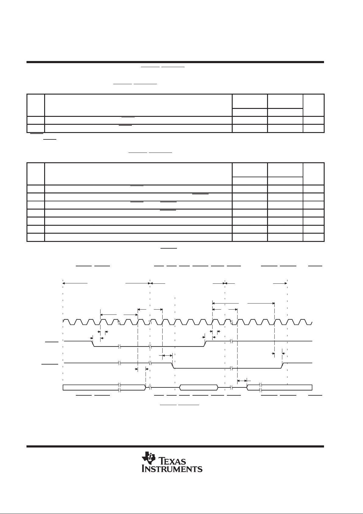
TMS320C6201, TMS320C6201B
DIGITAL SIGNAL PROCESSORS
SPRS051F – JANUARY 1997 – REVISED AUGUST 1999
46
POST OFFICE BOX 1443 • HOUSTON, TEXAS 77251–1443
HOLD/HOLDA TIMING
timing requirements for the HOLD
/HOLDA cycles† (see Figure 25)
NO.
’C6201-167
’C6201-200
’C6201B
UNIT
MIN MAX MIN MAX
1 t
su(HOLDH-CKO1H)
Setup time, HOLD high before CLKOUT1 high 5 1 ns
2 t
h(CKO1H-HOLDL)
Hold time, HOLD low after CLKOUT1 high 2 4 ns
†
HOLD
is synchronized internally. Therefore, if setup and hold times are not met, it will either be recognized in the current cycle or in the next cycle.
Thus, HOLD
can be an asynchronous input.
switching characteristics for the HOLD/HOLDA cycles‡ (see Figure 25)
NO. PARAMETER
’C6201-167
’C6201-200
’C6201B
UNIT
MIN MAX MIN MAX
3 t
R(HOLDL-BHZ)
Response time, HOLD low to EMIF Bus high impedance 4P
§
4P
§
ns
4 t
R(BHZ-HOLDAL)
Response time, EMIF Bus high impedance to HOLDA low P 2P P 2P ns
5 t
R(HOLDH-HOLDAH)
Response time, HOLD high to HOLDA high 4P 6P 4P 7P ns
6 t
d(CKO1H-HOLDAL)
Delay time, CLKOUT1 high to HOLDA valid –1 5 1 8 ns
7 t
d(CKO1H-BHZ)
Delay time, CLKOUT1 high to EMIF Bus high impedance
¶
–1 5 3 11 ns
8 t
d(CKO1H-BLZ)
Delay time, CLKOUT1 high to EMIF Bus low impedance
¶
–1 5 3 11 ns
9 t
R(HOLDH-BLZ)
Response time, HOLD high to EMIF Bus low impedance 3P 5P 3P 6P ns
‡
P = 1/CPU clock frequency in ns. For example, when running parts at 200 MHz, use P = 5 ns.
§
All pending EMIF transactions are allowed to complete before HOLDA
is asserted. The worst cases for this is an asynchronous read or write
with external ARDY used or a minimum of eight consecutive SDRAM reads or writes when RBTR8 = 1. If no bus transactions are occurring, then
the minimum delay time can be achieved. Also, bus hold can be indefinitely delayed by setting NOHOLD = 1.
¶
EMIF Bus consists of CE[3:0]
, BE[3:0], ED[31:0], EA[21:2], ARE, AOE, AWE, SSADS, SSOE, SSWE, SDA10, SDRAS, SDCAS, and SDWE.
DSP Owns Bus External Requester DSP Owns Bus
’C62x Ext Req ’C62x
8
7
3
4
6
6
1
2
CLKOUT1
HOLD
HOLDA
EMIF Bus
†
1
5
9
2
†
EMIF Bus consists of CE[3:0], BE[3:0], ED[31:0], EA[21:2], ARE, AOE, AWE, SSADS, SSOE, SSWE, SDA10, SDRAS, SDCAS, and SDWE.
Figure 25. HOLD/HOLDA Timing

TMS320C6201, TMS320C6201B
DIGITAL SIGNAL PROCESSORS
SPRS051F – JANUARY 1997 – REVISED AUGUST 1999
47
POST OFFICE BOX 1443 • HOUSTON, TEXAS 77251–1443
RESET TIMING
timing requirements for reset (see Figure 26)
NO.
’C6201-167
’C6201-200
’C6201B
UNIT
MIN MAX MIN MAX
1 t
w(RST
)
Width of the RESET pulse (PLL stable)
†
10 10
CLKOUT1
cycles
w(RST)
Width of the RESET pulse (PLL needs to sync up)
‡
250 250 µs
†
This parameter applies to CLKMODE x1 when CLKIN is stable and applies to CLKMODE x4 when CLKIN and PLL are stable.
‡
This parameter only applies to CLKMODE x4. The RESET
signal is not connected internally to the clock PLL circuit. The PLL, however, may
need up to 250 µs to stabilize following device power up or after PLL configuration has been changed. During that time, RESET
must be asserted
to ensure proper device operation. See the
clock PLL
section for PLL lock times.
switching characteristics during reset§¶ (see Figure 26)
NO. PARAMETER
’C6201-167
’C6201-200
’C6201B
UNIT
MIN MAX MIN MAX
2 t
R(RST)
Response time to change of value in RESET signal 2 2
CLKOUT1
cycles
3 t
d(CKO1H-CKO2IV)
Delay time, CLKOUT1 high to CLKOUT2 invalid –1 –1 ns
4 t
d(CKO1H-CKO2V)
Delay time, CLKOUT1 high to CLKOUT2 valid 10 10 ns
5 t
d(CKO1H-SDCLKIV)
Delay time, CLKOUT1 high to SDCLK invalid –1 –1 ns
6 t
d(CKO1H-SDCLKV)
Delay time, CLKOUT1 high to SDCLK valid 10 10 ns
7 t
d(CKO1H-SSCKIV)
Delay time, CLKOUT1 high to SSCLK invalid –1 –1 ns
8 t
d(CKO1H-SSCKV)
Delay time, CLKOUT1 high to SSCLK valid 10 10 ns
9 t
d(CKO1H-LOWIV)
Delay time, CLKOUT1 high to low group invalid –1 –1 ns
10 t
d(CKO1H-LOWV)
Delay time, CLKOUT1 high to low group valid 10 10 ns
11 t
d(CKO1H-HIGHIV)
Delay time, CLKOUT1 high to high group invalid –1 –1 ns
12 t
d(CKO1H-HIGHV)
Delay time, CLKOUT1 high to high group valid 10 10 ns
13 t
d(CKO1H-ZHZ)
Delay time, CLKOUT1 high to Z group high impedance –1 –1 ns
14 t
d(CKO1H-ZV)
Delay time, CLKOUT1 high to Z group valid 10 10 ns
§
Low group consists of: IACK, INUM[3:0], DMAC[3:0], PD, TOUT0, and TOUT1
High group consists of: HINT
Z group consists of: EA[21:2], ED[31:0], CE[3:0], BE[3:0], ARE, AWE, AOE, SSADS, SSOE, SSWE, SDA10, SDRAS, SDCAS,
SDWE
, HD[15:0], CLKX0, CLKX1, FSX0, FSX1, DX0, DX1, CLKR0, CLKR1, FSR0, and FSR1.
¶
HRDY
is gated by input HCS.
If HCS
= 0 at device reset, HRDY belongs to the high group.
If HCS
= 1 at device reset, HRDY belongs to the low group.

TMS320C6201, TMS320C6201B
DIGITAL SIGNAL PROCESSORS
SPRS051F – JANUARY 1997 – REVISED AUGUST 1999
48
POST OFFICE BOX 1443 • HOUSTON, TEXAS 77251–1443
RESET TIMING (CONTINUED)
1
22
1413
1211
109
87
65
43
CLKOUT1
RESET
CLKOUT2
SDCLK
SSCLK
LOW GROUP
†‡
HIGH GROUP
†‡
Z GROUP
†‡
†
Low group consists of: IACK, INUM[3:0], DMAC[3:0], PD, TOUT0, and TOUT1
High group consists of: HINT
Z group consists of: EA[21:2], ED[31:0], CE[3:0], BE[3:0], ARE, AWE, AOE, SSADS, SSOE, SSWE, SDA10, SDRAS, SDCAS,
SDWE
, HD[15:0], CLKX0, CLKX1, FSX0, FSX1, DX0, DX1, CLKR0, CLKR1, FSR0, and FSR1.
‡
HRDY
is gated by input HCS.
If HCS
= 0 at device reset, HRDY belongs to the high group.
If HCS
= 1 at device reset, HRDY belongs to the low group.
Figure 26. Reset Timing

TMS320C6201, TMS320C6201B
DIGITAL SIGNAL PROCESSORS
SPRS051F – JANUARY 1997 – REVISED AUGUST 1999
49
POST OFFICE BOX 1443 • HOUSTON, TEXAS 77251–1443
EXTERNAL INTERRUPT TIMING
timing requirements for interrupt response cycles
†‡
(see Figure 27)
NO.
’C6201-167
’C6201-200
’C6201B
UNIT
MIN MAX MIN MAX
2 t
w(ILOW)
Width of the interrupt pulse low 2P 2P ns
3 t
w(IHIGH)
Width of the interrupt pulse high 2P 2P ns
†
Interrupt signals are synchronized internally and are potentially recognized one cycle later if setup and hold times are violated. Thus, they can
be connected to asynchronous inputs.
‡
P = 1/CPU clock frequency in ns. For example, when running parts at 200 MHz, use P = 5 ns.
switching characteristics during interrupt response cycles§ (see Figure 27)
NO. PARAMETER
’C6201-167
’C6201-200
’C6201B
UNIT
MIN MAX MIN MAX
1 t
R(EINTH-IACKH)
Response time, EXT_INTx high to IACK high 9P 9P ns
4 t
d(CKO2L-IACKV)
Delay time, CLKOUT2 low to IACK valid 0 10 –4 – 0.5P 6 – 0.5P ns
5 t
d(CKO2L-INUMV)
Delay time, CLKOUT2 low to INUMx valid 10 6 – 0.5P ns
6 t
d(CKO2L-INUMIV)
Delay time, CLKOUT2 low to INUMx invalid 0 –4 – 0.5P ns
§
P = 1/CPU clock frequency in ns. For example, when running parts at 200 MHz, use P = 5 ns.
When the PLL is used (CLKMODE x4), 0.5P = 1/(2 × CPU clock frequency).
For CLKMODE x1: 0.5P = PH, where PH is the high period of CLKIN.
Interrupt Number
6
5
4
4
3
2
CLKOUT2
EXT_INTx, NMI
1
Intr Flag
IACK
INUMx
Figure 27. Interrupt Timing

TMS320C6201, TMS320C6201B
DIGITAL SIGNAL PROCESSORS
SPRS051F – JANUARY 1997 – REVISED AUGUST 1999
50
POST OFFICE BOX 1443 • HOUSTON, TEXAS 77251–1443
HOST-PORT INTERFACE TIMING
timing requirements for host-port interface cycles
†‡
(see Figure 28, Figure 29, Figure 30, and
Figure 31)
NO.
’C6201-167
’C6201-200
’C6201B
UNIT
MIN MAX MIN MAX
1 t
su(SEL-HSTBL)
Setup time, select signals§ valid before HSTROBE low 1 4 ns
2 t
h(HSTBL-SEL)
Hold time, select signals§ valid after HSTROBE low 2 2 ns
3 t
w(HSTBL)
Pulse duration, HSTROBE low 2P 2P ns
4 t
w(HSTBH)
Pulse duration, HSTROBE high between consecutive accesses 2P 2P ns
10 t
su(SEL-HASL)
Setup time, select signals§ valid before HAS low 1 4 ns
11 t
h(HASL-SEL)
Hold time, select signals§ valid after HAS low 2 2 ns
12 t
su(HDV-HSTBH)
Setup time, host data valid before HSTROBE high 1 3 ns
13 t
h(HSTBH-HDV)
Hold time, host data valid after HSTROBE high 1 2 ns
14 t
h(HRDYL-HSTBL)
Hold time, HSTROBE low after HRDY low. HSTROBE shoul
not be inactivated until HRDY
is active (low); otherwise, HPI
writes will not complete properly.
1 1 ns
18 t
su(HASL-HSTBL)
Setup time, HAS low before HSTROBE low 2 2 ns
19 t
h(HSTBL-HASL)
Hold time, HAS low after HSTROBE low 2 2 ns
†
HSTROBE
refers to the following logical operation on HCS, HDS1, and HDS2: [NOT(HDS1 XOR HDS2)] OR HCS.
‡
The effects of internal clock jitter are included at test. There is no need to adjust timing numbers for internal clock jitter. P = 1/CPU clock frequency
in ns. For example, when running parts at 200 MHz, use P = 5 ns.
§
Select signals include: HCNTRL[1:0], HR/W
, and HHWIL.
switching characteristics during host-port interface cycles†‡ (see Figure 28, Figure 29, Figure 30,
and Figure 31)
NO. PARAMETER
’C6201-167
’C6201-200
’C6201B
UNIT
MIN MAX MIN MAX
5 t
d(HCS-HRDY)
Delay time, HCS to HRDY
¶
1 7 1 9 ns
6 t
d(HSTBL-HRDYH)
Delay time, HSTROBE low to HRDY high
#
3 12 3 12 ns
7 t
oh(HSTBL-HDLZ)
Output hold time, HD low impedance after HSTROBE low
for an HPI read
4 4 ns
8 t
d(HDV-HRDYL)
Delay time, HD valid to HRDY low P – 2 P P – 3 P + 3 ns
9 t
oh(HSTBH-HDV)
Output hold time, HD valid after HSTROBE high 3 12 2 12 ns
15 t
d(HSTBH-HDHZ)
Delay time, HSTROBE high to HD high impedance 3 12 3 12 ns
16 t
d(HSTBL-HDV)
Delay time, HSTROBE low to HD valid 3 12 2 12 ns
17 t
d(HSTBH-HRDYH)
Delay time, HSTROBE high to HRDY high
||
3 12 3 12 ns
†
HSTROBE refers to the following logical operation on HCS, HDS1, and HDS2: [NOT(HDS1 XOR HDS2)] OR HCS.
‡
The effects of internal clock jitter are included at test. There is no need to adjust timing numbers for internal clock jitter. P = 1/CPU clock frequency
in ns. For example, when running parts at 200 MHz, use P = 5 ns.
¶
HCS
enables HRDY, and HRDY is always low when HCS is high. The case where HRDY goes high when HCS falls indicates that HPI is busy
completing a previous HPID write or READ with autoincrement.
#
This parameter is used during an HPID read. At the beginning of the first half-word transfer on the falling edge of HSTROBE
, the HPI sends the
request to the DMA auxiliary channel, and HRDY
remains high until the DMA auxiliary channel loads the requested data into HPID.
||
This parameter is used after the second half-word of an HPID write or autoincrement read. HRDY
remains low if the access is not an HPID write
or autoincrement read. Reading or writing to HPIC or HPIA does not affect the HRDY
signal.

TMS320C6201, TMS320C6201B
DIGITAL SIGNAL PROCESSORS
SPRS051F – JANUARY 1997 – REVISED AUGUST 1999
51
POST OFFICE BOX 1443 • HOUSTON, TEXAS 77251–1443
HOST-PORT INTERFACE TIMING (CONTINUED)
1st Half-Word 2nd Half-Word
5
17
86
5
17
85
15
916
15
97
4
3
2
1
2
1
2
1
2
1
2
1
2
1
HAS
HCNTL[1:0]
HR/W
HHWIL
HSTROBE
†
HCS
HD[15:0] (output)
HRDY (case 1)
HRDY
(case 2)
3
†
HSTROBE refers to the following logical operation on HCS, HDS1, and HDS2: [NOT(HDS1 XOR HDS2)] OR HCS.
Figure 28. HPI Read Timing (HAS Not Used, Tied High)
HAS
HCNTL[1:0]
HR/W
HHWIL
HSTROBE
†
HCS
HD[15:0] (output)
HRDY (case 1)
HRDY
(case 2)
1st half-word 2nd half-word
51786
51785
15
916
15
97
4
3
11
10
11
10
11
10
11
10
11
1011
10
19
19
18
18
†
HSTROBE
refers to the following logical operation on HCS, HDS1, and HDS2: [NOT(HDS1 XOR HDS2)] OR HCS.
Figure 29. HPI Read Timing (HAS Used)

TMS320C6201, TMS320C6201B
DIGITAL SIGNAL PROCESSORS
SPRS051F – JANUARY 1997 – REVISED AUGUST 1999
52
POST OFFICE BOX 1443 • HOUSTON, TEXAS 77251–1443
HOST-PORT INTERFACE TIMING (CONTINUED)
1st Half-Word 2nd Half-Word
5
17
5
13
12
13
12
4
14
3
2
1
2
1
2
1
2
1
13
12
13
12
2
1
2
1
HAS
HCNTL[1:0]
HR/W
HHWIL
HSTROBE
†
HCS
HD[15:0] (input)
HRDY
HBE[1:0]
3
†
HSTROBE refers to the following logical operation on HCS, HDS1, and HDS2: [NOT(HDS1 XOR HDS2)] OR HCS.
Figure 30. HPI Write Timing (HAS Not Used, Tied High)
1st half-word 2nd half-word
5
17
5
13
12
13
12
4
14
3
11
10
11
10
11
10
11
10
11
10
11
10
13
12
13
12
HAS
HCNTL[1:0]
HR/W
HHWIL
HSTROBE
†
HCS
HD[15:0] (input)
HRDY
HBE[1:0]
19
19
18
18
†
HSTROBE
refers to the following logical operation on HCS, HDS1, and HDS2: [NOT(HDS1 XOR HDS2)] OR HCS.
Figure 31. HPI Write Timing (HAS Used)

TMS320C6201, TMS320C6201B
DIGITAL SIGNAL PROCESSORS
SPRS051F – JANUARY 1997 – REVISED AUGUST 1999
53
POST OFFICE BOX 1443 • HOUSTON, TEXAS 77251–1443
MULTICHANNEL BUFFERED SERIAL PORT TIMING
timing requirements for McBSP
†‡
(see Figure 32)
NO.
’C6201-167
’C6201-200
’C6201B
UNIT
MIN MAX MIN MAX
2 t
c(CKRX)
Cycle time, CLKR/X CLKR/X ext 2P 2P ns
3 t
w(CKRX)
Pulse duration, CLKR/X high or CLKR/X low CLKR/X ext P – 1 P – 1 ns
p
CLKR int 13 9
5
t
su(FRH-CKRL)
Setup time, external FSR high before CLKR lo
w
CLKR ext
4 2
ns
CLKR int 7 6
6
t
h(CKRL-FRH)
Hold time, external FSR high after CLKR lo
w
CLKR ext
3 3
ns
p
CLKR int 10 8
7
t
su(DRV-CKRL)
Setup time, DR valid before CLKR lo
w
CLKR ext
1 0
ns
CLKR int 4 3
8
t
h(CKRL-DRV)
Hold time, DR valid after CLKR lo
w
CLKR ext
4 4
ns
p
CLKX int 13 9
10
t
su(FXH-CKXL)
Setup time, external FSX high before CLKX lo
w
CLKX ext
4 2
ns
CLKX int 7 6
11
t
h(CKXL-FXH)
Hold time, external FSX high after CLKX lo
w
CLKX ext 3 3
ns
†
CLKRP = CLKXP = FSRP = FSXP = 0. If polarity of any of the signals is inverted, then the timing references of that signal are also inverted.
‡
P = 1/CPU clock frequency in ns. For example, when running parts at 200 MHz, use P = 5 ns.

TMS320C6201, TMS320C6201B
DIGITAL SIGNAL PROCESSORS
SPRS051F – JANUARY 1997 – REVISED AUGUST 1999
54
POST OFFICE BOX 1443 • HOUSTON, TEXAS 77251–1443
MULTICHANNEL BUFFERED SERIAL PORT TIMING (CONTINUED)
switching characteristics for McBSP
†‡§
(see Figure 32)
NO. PARAMETER
’C6201-167
’C6201-200
’C6201B
UNIT
MIN MAX MIN MAX
1 t
d(CKSH-CKRXH)
Delay time, CLKS high to CLKR/X high for
internal CLKR/X generated from CLKS
input
4 15 3 10 ns
2 t
c(CKRX)
Cycle time, CLKR/X CLKR/X int 2P 2P ns
3 t
w(CKRX)
Pulse duration, CLKR/X high or CLKR/X
low
CLKR/X int C – 1¶C + 1¶C – 1.3¶C + 1
¶
ns
4 t
d(CKRH-FRV)
Delay time, CLKR high to internal FSR
valid
CLKR int –2 4 –2 3 ns
Delay time, CLKX high to internal FSX
CLKX int 0 4 –2 3
9
t
d(CKXH-FXV)
y, g
valid
CLKX ext
3 16 3 9
ns
Disable time, DX high impedance follow-
CLKX int 0 4 –1 4
12
t
dis(CKXH-DXHZ)
,g
ing last data bit from CLKX high
CLKX ext
3 16 3 9
ns
CLKX int 0 4 –1 4
13
t
d(CKXH-DXV)
Delay time, CLKX high to DX valid
CLKX ext 3 16 3 9
ns
Delay time, FSX high to DX valid
FSX int –2 4 –1 3
14
t
d(FXH-DXV)
ONLY applies when in data
delay 0 (XDATDLY = 00b) mode
FSX ext 3 16 3 9
ns
†
CLKRP = CLKXP = FSRP = FSXP = 0. If polarity of any of the signals is inverted, then the timing references of that signal are also inverted.
‡
Minimum delay times also represent minimum output hold times.
§
P = 1/CPU clock frequency in ns. For example, when running parts at 200 MHz, use P = 5 ns.
¶
C = H or L
S = sample rate generator input clock = P if CLKSM = 1 (P = 1/CPU clock frequency)
= sample rate generator input clock = P_clks if CLKSM = 0 (P_clks = CLKS period)
H = CLKX high pulse width = (CLKGDV/2 + 1) * S if CLKGDV is even
= (CLKGDV + 1)/2 * S if CLKGDV is odd or zero
L = CLKX low pulse width = (CLKGDV/2) * S if CLKGDV is even
= (CLKGDV + 1)/2 * S if CLKGDV is odd or zero

TMS320C6201, TMS320C6201B
DIGITAL SIGNAL PROCESSORS
SPRS051F – JANUARY 1997 – REVISED AUGUST 1999
55
POST OFFICE BOX 1443 • HOUSTON, TEXAS 77251–1443
MULTICHANNEL BUFFERED SERIAL PORT TIMING (CONTINUED)
Bit(n-1) (n-2) (n-3)
Bit 0 Bit(n-1) (n-2) (n-3)
14
1312
11
10
9
3
3
2
8
7
6
5
4
4
3
1
3
2
CLKS
CLKR
FSR (int)
FSR (ext)
DR
CLKX
FSX (int)
FSX (ext)
FSX (XDATDLY=00b)
DX
13
Figure 32. McBSP Timings

TMS320C6201, TMS320C6201B
DIGITAL SIGNAL PROCESSORS
SPRS051F – JANUARY 1997 – REVISED AUGUST 1999
56
POST OFFICE BOX 1443 • HOUSTON, TEXAS 77251–1443
MULTICHANNEL BUFFERED SERIAL PORT TIMING (CONTINUED)
timing requirements for FSR when GSYNC = 1 (see Figure 33)
NO.
’C6201-167
’C6201-200
’C6201B
UNIT
MIN MAX MIN MAX
1 t
su(FRH-CKSH)
Setup time, FSR high before CLKS high 4 4 ns
2 t
h(CKSH-FRH)
Hold time, FSR high after CLKS high 4 4 ns
2
1
CLKS
FSR External
CLKR/X (no need to resync)
CLKR/X (needs resync)
Figure 33. FSR Timing When GSYNC = 1

TMS320C6201, TMS320C6201B
DIGITAL SIGNAL PROCESSORS
SPRS051F – JANUARY 1997 – REVISED AUGUST 1999
57
POST OFFICE BOX 1443 • HOUSTON, TEXAS 77251–1443
MULTICHANNEL BUFFERED SERIAL PORT TIMING (CONTINUED)
timing requirements for McBSP as SPI master or slave: CLKSTP = 10b, CLKXP = 0
†‡
(see Figure 34)
(’C6201)
’C6201-167
’C6201-200
NO.
MASTER SLAVE
UNIT
MIN MAX MIN MAX
4 t
su(DRV-CKXL)
Setup time, DR valid before CLKX low 12 2 – 3P ns
5 t
h(CKXL-DRV)
Hold time, DR valid after CLKX low 4 5 + 6P ns
†
P = 1/CPU clock frequency in ns. For example, when running parts at 200 MHz, use P = 5 ns.
‡
For all SPI slave modes, CLKG is programmed as 1/2 of the CPU clock by setting CLKSM = CLKGDV = 1.
switching characteristics for McBSP as SPI master or slave: CLKSTP = 10b, CLKXP = 0
†‡
(see Figure 34) (’C6201)
’C6201-167
’C6201-200
NO. PARAMETER
MASTER
§
SLAVE
UNIT
MIN MAX MIN MAX
1 t
h(CKXL-FXL)
Hold time, FSX low after CLKX low
¶
T – 2 T + 3 ns
2 t
d(FXL-CKXH)
Delay time, FSX low to CLKX high
#
L – 2 L + 3 ns
3 t
d(CKXH-DXV)
Delay time, CLKX high to DX valid –2 4 3P + 4 5P + 17 ns
6 t
dis(CKXL-DXHZ)
Disable time, DX high impedance following last data bit from
CLKX low
L – 2 L + 3 ns
7 t
dis(FXH-DXHZ)
Disable time, DX high impedance following last data bit from
FSX high
P + 4 3P + 17 ns
8 t
d(FXL-DXV)
Delay time, FSX low to DX valid 2P + 4 4P + 17 ns
†
P = 1/CPU clock frequency in ns. For example, when running parts at 200 MHz, use P = 5 ns.
‡
For all SPI slave modes, CLKG is programmed as 1/2 of the CPU clock by setting CLKSM = CLKGDV = 1.
§
S = sample rate generator input clock = P if CLKSM = 1 (P = 1/CPU clock frequency)
= sample rate generator input clock = P_clks if CLKSM = 0 (P_clks = CLKS period)
T = CLKX period = (1 + CLKGDV) * S
H = CLKX high pulse width = (CLKGDV/2 + 1) * S if CLKGDV is even
= (CLKGDV + 1)/2 * S if CLKGDV is odd or zero
L = CLKX low pulse width = (CLKGDV/2) * S if CLKGDV is even
= (CLKGDV + 1)/2 * S if CLKGDV is odd or zero
¶
FSRP = FSXP = 1. As a SPI master, FSX is inverted to provide active-low slave-enable output. As a slave, the active-low signal input on FSX
and FSR is inverted before being used internally.
CLKXM = FSXM = 1, CLKRM = FSRM = 0 for master McBSP
CLKXM = CLKRM = FSXM = FSRM = 0 for slave McBSP
#
FSX should be low before the rising edge of clock to enable slave devices and then begin a SPI transfer at the rising edge of the master clock
(CLKX).

TMS320C6201, TMS320C6201B
DIGITAL SIGNAL PROCESSORS
SPRS051F – JANUARY 1997 – REVISED AUGUST 1999
58
POST OFFICE BOX 1443 • HOUSTON, TEXAS 77251–1443
MULTICHANNEL BUFFERED SERIAL PORT TIMING (CONTINUED)
timing requirements for McBSP as SPI master or slave: CLKSTP = 10b, CLKXP = 0
†‡
(see Figure 34) (’C6201B)
’C6201B
NO.
MASTER SLAVE
UNIT
MIN MAX MIN MAX
4 t
su(DRV-CKXL)
Setup time, DR valid before CLKX low 12 2 – 3P ns
5 t
h(CKXL-DRV)
Hold time, DR valid after CLKX low 4 5 + 6P ns
†
P = 1/CPU clock frequency in ns. For example, when running parts at 200 MHz, use P = 5 ns.
‡
For all SPI slave modes, CLKG is programmed as 1/2 of the CPU clock by setting CLKSM = CLKGDV = 1.
switching characteristics for McBSP as SPI master or slave: CLKSTP = 10b, CLKXP = 0
†‡
(see Figure 34) (’C6201B)
’C6201B
NO. PARAMETER
MASTER
§
SLAVE
UNIT
MIN MAX MIN MAX
1 t
h(CKXL-FXL)
Hold time, FSX low after CLKX low
¶
T – 2 T + 3 ns
2 t
d(FXL-CKXH)
Delay time, FSX low to CLKX high
#
L – 2 L + 3 ns
3 t
d(CKXH-DXV)
Delay time, CLKX high to DX valid –2 4 3P + 4 5P + 17 ns
6 t
dis(CKXL-DXHZ)
Disable time, DX high impedance following last data bit from
CLKX low
L – 2 L + 3 ns
7 t
dis(FXH-DXHZ)
Disable time, DX high impedance following last data bit from
FSX high
P + 3 3P + 17 ns
8 t
d(FXL-DXV)
Delay time, FSX low to DX valid 2P + 2 4P + 17 ns
†
P = 1/CPU clock frequency in ns. For example, when running parts at 200 MHz, use P = 5 ns.
‡
For all SPI slave modes, CLKG is programmed as 1/2 of the CPU clock by setting CLKSM = CLKGDV = 1.
§
S = sample rate generator input clock = P if CLKSM = 1 (P = 1/CPU clock frequency)
= sample rate generator input clock = P_clks if CLKSM = 0 (P_clks = CLKS period)
T = CLKX period = (1 + CLKGDV) * S
H = CLKX high pulse width = (CLKGDV/2 + 1) * S if CLKGDV is even
= (CLKGDV + 1)/2 * S if CLKGDV is odd or zero
L = CLKX low pulse width = (CLKGDV/2) * S if CLKGDV is even
= (CLKGDV + 1)/2 * S if CLKGDV is odd or zero
¶
FSRP = FSXP = 1. As a SPI master, FSX is inverted to provide active-low slave-enable output. As a slave, the active-low signal input on FSX
and FSR is inverted before being used internally.
CLKXM = FSXM = 1, CLKRM = FSRM = 0 for master McBSP
CLKXM = CLKRM = FSXM = FSRM = 0 for slave McBSP
#
FSX should be low before the rising edge of clock to enable slave devices and then begin a SPI transfer at the rising edge of the master clock
(CLKX).

TMS320C6201, TMS320C6201B
DIGITAL SIGNAL PROCESSORS
SPRS051F – JANUARY 1997 – REVISED AUGUST 1999
59
POST OFFICE BOX 1443 • HOUSTON, TEXAS 77251–1443
MULTICHANNEL BUFFERED SERIAL PORT TIMING (CONTINUED)
Bit 0 Bit(n-1) (n-2) (n-3) (n-4)
Bit 0 Bit(n-1) (n-2) (n-3) (n-4)
5
4
3
87
6
21
CLKX
FSX
DX
DR
Figure 34. McBSP Timing as SPI Master or Slave: CLKSTP = 10b, CLKXP = 0

TMS320C6201, TMS320C6201B
DIGITAL SIGNAL PROCESSORS
SPRS051F – JANUARY 1997 – REVISED AUGUST 1999
60
POST OFFICE BOX 1443 • HOUSTON, TEXAS 77251–1443
MULTICHANNEL BUFFERED SERIAL PORT TIMING (CONTINUED)
timing requirements for McBSP as SPI master or slave: CLKSTP = 11b, CLKXP = 0
†‡
(see Figure 35)
(’C6201)
’C6201-167
’C6201-200
NO.
MASTER SLAVE
UNIT
MIN MAX MIN MAX
4 t
su(DRV-CKXH)
Setup time, DR valid before CLKX high 12 2 – 3P ns
5 t
h(CKXH-DRV)
Hold time, DR valid after CLKX high 4 5 + 6P ns
†
P = 1/CPU clock frequency in ns. For example, when running parts at 200 MHz, use P = 5 ns.
‡
For all SPI slave modes, CLKG is programmed as 1/2 of the CPU clock by setting CLKSM = CLKGDV = 1.
switching characteristics for McBSP as SPI master or slave: CLKSTP = 11b, CLKXP = 0
†‡
(see Figure 35) (’C6201)
’C6201-167
’C6201-200
NO. PARAMETER
MASTER
§
SLAVE
UNIT
MIN MAX MIN MAX
1 t
h(CKXL-FXL)
Hold time, FSX low after CLKX low
¶
L – 2 L + 3 ns
2 t
d(FXL-CKXH)
Delay time, FSX low to CLKX high
#
T – 2 T + 3 ns
3 t
d(CKXL-DXV)
Delay time, CLKX low to DX valid –2 4 3P + 4 5P + 17 ns
6 t
dis(CKXL-DXHZ)
Disable time, DX high impedance following last data bit from
CLKX low
–2 4 3P + 4 5P + 17 ns
7 t
d(FXL-DXV)
Delay time, FSX low to DX valid H – 2 H + 4 2P + 4 4P + 17 ns
†
P = 1/CPU clock frequency in ns. For example, when running parts at 200 MHz, use P = 5 ns.
‡
For all SPI slave modes, CLKG is programmed as 1/2 of the CPU clock by setting CLKSM = CLKGDV = 1.
§
S = sample rate generator input clock = P if CLKSM = 1 (P = 1/CPU clock frequency)
= sample rate generator input clock = P_clks if CLKSM = 0 (P_clks = CLKS period)
T = CLKX period = (1 + CLKGDV) * S
H = CLKX high pulse width = (CLKGDV/2 + 1) * S if CLKGDV is even
= (CLKGDV + 1)/2 * S if CLKGDV is odd or zero
L = CLKX low pulse width = (CLKGDV/2) * S if CLKGDV is even
= (CLKGDV + 1)/2 * S if CLKGDV is odd or zero
¶
FSRP = FSXP = 1. As a SPI master, FSX is inverted to provide active-low slave-enable output. As a slave, the active-low signal input on FSX
and FSR is inverted before being used internally.
CLKXM = FSXM = 1, CLKRM = FSRM = 0 for master McBSP
CLKXM = CLKRM = FSXM = FSRM = 0 for slave McBSP
#
FSX should be low before the rising edge of clock to enable slave devices and then begin a SPI transfer at the rising edge of the master clock
(CLKX).
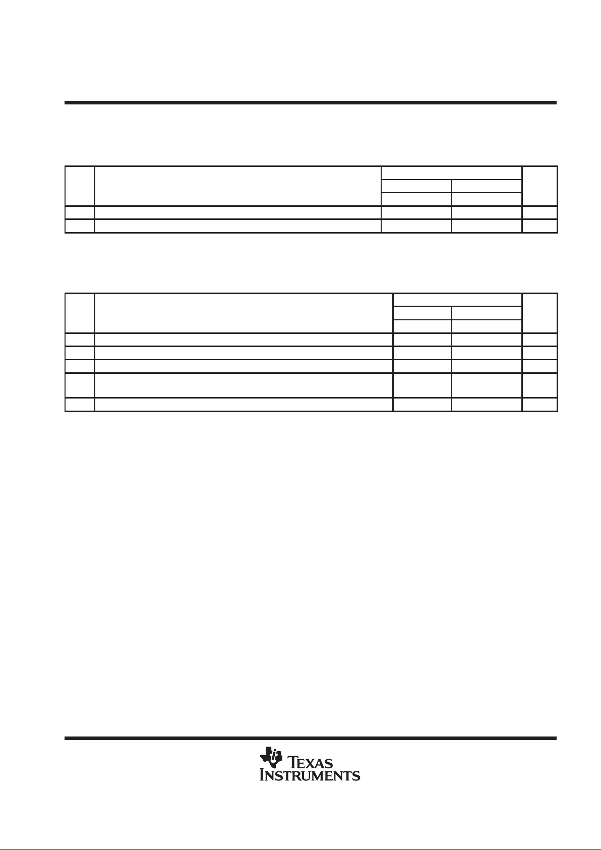
TMS320C6201, TMS320C6201B
DIGITAL SIGNAL PROCESSORS
SPRS051F – JANUARY 1997 – REVISED AUGUST 1999
61
POST OFFICE BOX 1443 • HOUSTON, TEXAS 77251–1443
MULTICHANNEL BUFFERED SERIAL PORT TIMING (CONTINUED)
timing requirements for McBSP as SPI master or slave: CLKSTP = 11b, CLKXP = 0
†‡
(see Figure 35)
(’C6201B)
’C6201B
NO.
MASTER SLAVE
UNIT
MIN MAX MIN MAX
4 t
su(DRV-CKXH)
Setup time, DR valid before CLKX high 12 2 – 3P ns
5 t
h(CKXH-DRV)
Hold time, DR valid after CLKX high 4 5 + 6P ns
†
P = 1/CPU clock frequency in ns. For example, when running parts at 200 MHz, use P = 5 ns.
‡
For all SPI slave modes, CLKG is programmed as 1/2 of the CPU clock by setting CLKSM = CLKGDV = 1.
switching characteristics for McBSP as SPI master or slave: CLKSTP = 11b, CLKXP = 0
†‡
(see Figure 35) (’C6201B)
’C6201B
NO. PARAMETER
MASTER
§
SLAVE
UNIT
MIN MAX MIN MAX
1 t
h(CKXL-FXL)
Hold time, FSX low after CLKX low
¶
L – 2 L + 3 ns
2 t
d(FXL-CKXH)
Delay time, FSX low to CLKX high
#
T – 2 T + 3 ns
3 t
d(CKXL-DXV)
Delay time, CLKX low to DX valid –2 4 3P + 4 5P + 17 ns
6 t
dis(CKXL-DXHZ)
Disable time, DX high impedance following last data bit from
CLKX low
–2 4 3P + 3 5P + 17 ns
7 t
d(FXL-DXV)
Delay time, FSX low to DX valid H – 2 H + 4 2P + 2 4P + 17 ns
†
P = 1/CPU clock frequency in ns. For example, when running parts at 200 MHz, use P = 5 ns.
‡
For all SPI slave modes, CLKG is programmed as 1/2 of the CPU clock by setting CLKSM = CLKGDV = 1.
§
S = sample rate generator input clock = P if CLKSM = 1 (P = 1/CPU clock frequency)
= sample rate generator input clock = P_clks if CLKSM = 0 (P_clks = CLKS period)
T = CLKX period = (1 + CLKGDV) * S
H = CLKX high pulse width = (CLKGDV/2 + 1) * S if CLKGDV is even
= (CLKGDV + 1)/2 * S if CLKGDV is odd or zero
L = CLKX low pulse width = (CLKGDV/2) * S if CLKGDV is even
= (CLKGDV + 1)/2 * S if CLKGDV is odd or zero
¶
FSRP = FSXP = 1. As a SPI master, FSX is inverted to provide active-low slave-enable output. As a slave, the active-low signal input on FSX
and FSR is inverted before being used internally.
CLKXM = FSXM = 1, CLKRM = FSRM = 0 for master McBSP
CLKXM = CLKRM = FSXM = FSRM = 0 for slave McBSP
#
FSX should be low before the rising edge of clock to enable slave devices and then begin a SPI transfer at the rising edge of the master clock
(CLKX).
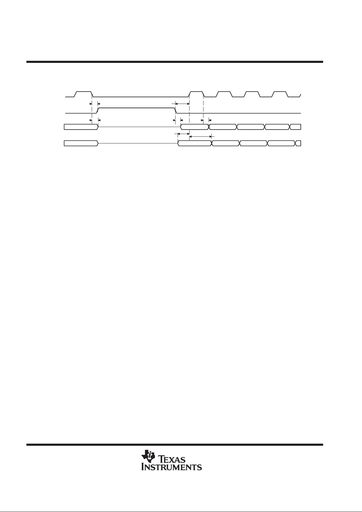
TMS320C6201, TMS320C6201B
DIGITAL SIGNAL PROCESSORS
SPRS051F – JANUARY 1997 – REVISED AUGUST 1999
62
POST OFFICE BOX 1443 • HOUSTON, TEXAS 77251–1443
MULTICHANNEL BUFFERED SERIAL PORT TIMING (CONTINUED)
Bit 0 Bit(n-1) (n-2) (n-3) (n-4)
Bit 0 Bit(n-1) (n-2) (n-3) (n-4)
4
376
21
CLKX
FSX
DX
DR
5
Figure 35. McBSP Timing as SPI Master or Slave: CLKSTP = 11b, CLKXP = 0

TMS320C6201, TMS320C6201B
DIGITAL SIGNAL PROCESSORS
SPRS051F – JANUARY 1997 – REVISED AUGUST 1999
63
POST OFFICE BOX 1443 • HOUSTON, TEXAS 77251–1443
MULTICHANNEL BUFFERED SERIAL PORT TIMING (CONTINUED)
timing requirements for McBSP as SPI master or slave: CLKSTP = 10b, CLKXP = 1
†‡
(see Figure 36)
(’C6201)
’C6201-167
’C6201-200
NO.
MASTER SLAVE
UNIT
MIN MAX MIN MAX
4 t
su(DRV-CKXH)
Setup time, DR valid before CLKX high 12 2 – 3P ns
5 t
h(CKXH-DRV)
Hold time, DR valid after CLKX high 4 5 + 6P ns
†
P = 1/CPU clock frequency in ns. For example, when running parts at 200 MHz, use P = 5 ns.
‡
For all SPI slave modes, CLKG is programmed as 1/2 of the CPU clock by setting CLKSM = CLKGDV = 1.
switching characteristics for McBSP as SPI master or slave: CLKSTP = 10b, CLKXP = 1
†‡
(see Figure 36) (’C6201)
’C6201-167
’C6201-200
NO. PARAMETER
MASTER
§
SLAVE
UNIT
MIN MAX MIN MAX
1 t
h(CKXH-FXL)
Hold time, FSX low after CLKX high
¶
T – 2 T + 3 ns
2 t
d(FXL-CKXL)
Delay time, FSX low to CLKX low
#
H – 2 H + 3 ns
3 t
d(CKXL-DXV)
Delay time, CLKX low to DX valid –2 4 3P + 4 5P + 17 ns
6 t
dis(CKXH-DXHZ)
Disable time, DX high impedance following last data bit from
CLKX high
H – 2 H + 3 ns
7 t
dis(FXH-DXHZ)
Disable time, DX high impedance following last data bit from
FSX high
P + 4 3P + 17 ns
8 t
d(FXL-DXV)
Delay time, FSX low to DX valid 2P + 4 4P + 17 ns
†
P = 1/CPU clock frequency in ns. For example, when running parts at 200 MHz, use P = 5 ns.
‡
For all SPI slave modes, CLKG is programmed as 1/2 of the CPU clock by setting CLKSM = CLKGDV = 1.
§
S = sample rate generator input clock = P if CLKSM = 1 (P = 1/CPU clock frequency)
= sample rate generator input clock = P_clks if CLKSM = 0 (P_clks = CLKS period)
T = CLKX period = (1 + CLKGDV) * S
H = CLKX high pulse width = (CLKGDV/2 + 1) * S if CLKGDV is even
= (CLKGDV + 1)/2 * S if CLKGDV is odd or zero
L = CLKX low pulse width = (CLKGDV/2) * S if CLKGDV is even
= (CLKGDV + 1)/2 * S if CLKGDV is odd or zero
¶
FSRP = FSXP = 1. As a SPI master, FSX is inverted to provide active-low slave-enable output. As a slave, the active-low signal input on FSX
and FSR is inverted before being used internally.
CLKXM = FSXM = 1, CLKRM = FSRM = 0 for master McBSP
CLKXM = CLKRM = FSXM = FSRM = 0 for slave McBSP
#
FSX should be low before the rising edge of clock to enable slave devices and then begin a SPI transfer at the rising edge of the master clock
(CLKX).

TMS320C6201, TMS320C6201B
DIGITAL SIGNAL PROCESSORS
SPRS051F – JANUARY 1997 – REVISED AUGUST 1999
64
POST OFFICE BOX 1443 • HOUSTON, TEXAS 77251–1443
MULTICHANNEL BUFFERED SERIAL PORT TIMING (CONTINUED)
timing requirements for McBSP as SPI master or slave: CLKSTP = 10b, CLKXP = 1
†‡
(see Figure 36)
(’C6201B)
’C6201B
NO.
MASTER SLAVE
UNIT
MIN MAX MIN MAX
4 t
su(DRV-CKXH)
Setup time, DR valid before CLKX high 12 2 – 3P ns
5 t
h(CKXH-DRV)
Hold time, DR valid after CLKX high 4 5 + 6P ns
†
P = 1/CPU clock frequency in ns. For example, when running parts at 200 MHz, use P = 5 ns.
‡
For all SPI slave modes, CLKG is programmed as 1/2 of the CPU clock by setting CLKSM = CLKGDV = 1.
switching characteristics for McBSP as SPI master or slave: CLKSTP = 10b, CLKXP = 1
†‡
(see Figure 36) (’C6201B)
’C6201B
NO. PARAMETER
MASTER
§
SLAVE
UNIT
MIN MAX MIN MAX
1 t
h(CKXH-FXL)
Hold time, FSX low after CLKX high
¶
T – 2 T + 3 ns
2 t
d(FXL-CKXL)
Delay time, FSX low to CLKX low
#
H – 2 H + 3 ns
3 t
d(CKXL-DXV)
Delay time, CLKX low to DX valid –2 4 3P + 4 5P + 17 ns
6 t
dis(CKXH-DXHZ)
Disable time, DX high impedance following last data bit from
CLKX high
H – 2 H + 3 ns
7 t
dis(FXH-DXHZ)
Disable time, DX high impedance following last data bit from
FSX high
P + 3 3P + 17 ns
8 t
d(FXL-DXV)
Delay time, FSX low to DX valid 2P + 2 4P + 17 ns
†
P = 1/CPU clock frequency in ns. For example, when running parts at 200 MHz, use P = 5 ns.
‡
For all SPI slave modes, CLKG is programmed as 1/2 of the CPU clock by setting CLKSM = CLKGDV = 1.
§
S = sample rate generator input clock = P if CLKSM = 1 (P = 1/CPU clock frequency)
= sample rate generator input clock = P_clks if CLKSM = 0 (P_clks = CLKS period)
T = CLKX period = (1 + CLKGDV) * S
H = CLKX high pulse width = (CLKGDV/2 + 1) * S if CLKGDV is even
= (CLKGDV + 1)/2 * S if CLKGDV is odd or zero
L = CLKX low pulse width = (CLKGDV/2) * S if CLKGDV is even
= (CLKGDV + 1)/2 * S if CLKGDV is odd or zero
¶
FSRP = FSXP = 1. As a SPI master, FSX is inverted to provide active-low slave-enable output. As a slave, the active-low signal input on FSX
and FSR is inverted before being used internally.
CLKXM = FSXM = 1, CLKRM = FSRM = 0 for master McBSP
CLKXM = CLKRM = FSXM = FSRM = 0 for slave McBSP
#
FSX should be low before the rising edge of clock to enable slave devices and then begin a SPI transfer at the rising edge of the master clock
(CLKX).
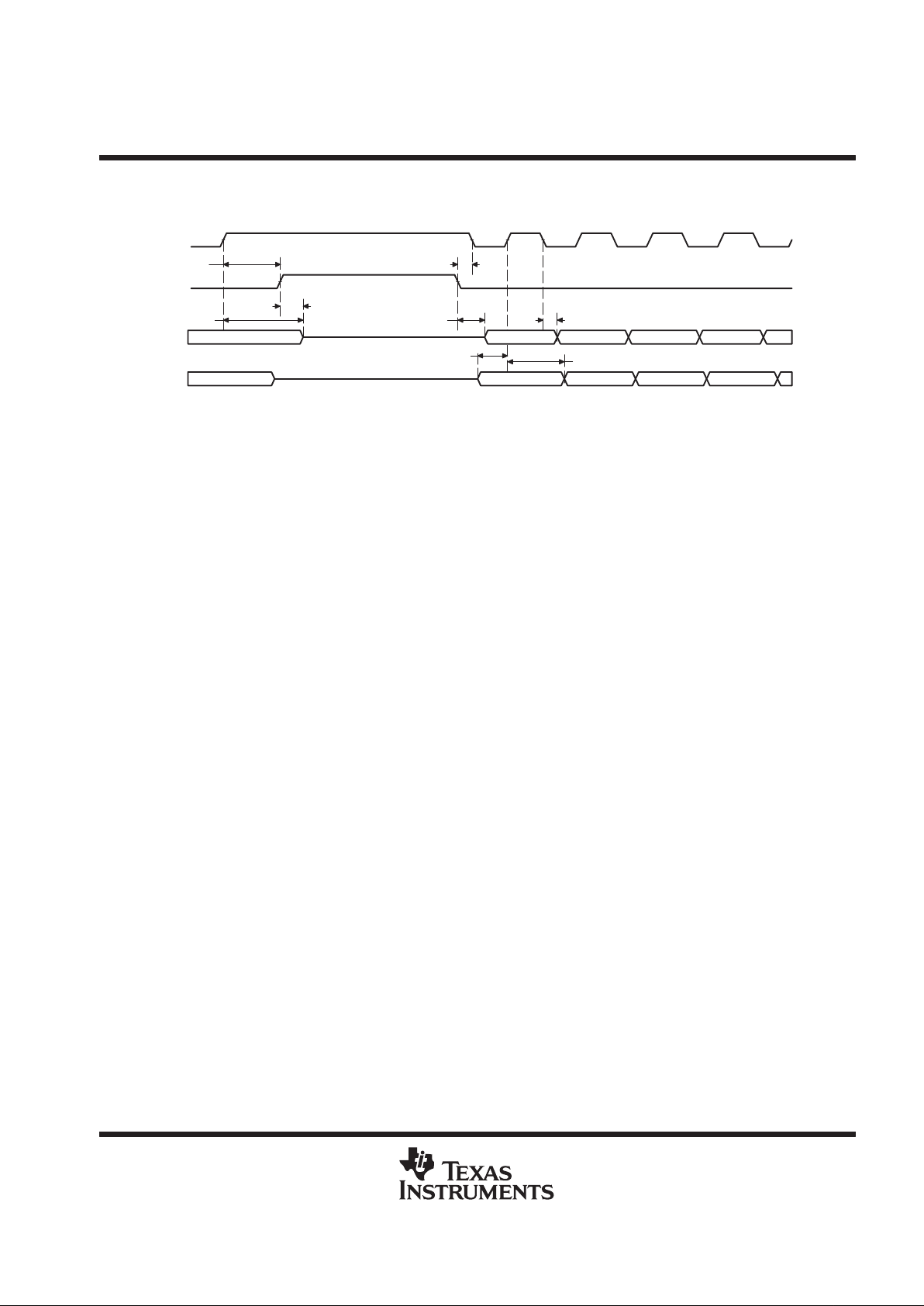
TMS320C6201, TMS320C6201B
DIGITAL SIGNAL PROCESSORS
SPRS051F – JANUARY 1997 – REVISED AUGUST 1999
65
POST OFFICE BOX 1443 • HOUSTON, TEXAS 77251–1443
MULTICHANNEL BUFFERED SERIAL PORT TIMING (CONTINUED)
Bit 0 Bit(n-1) (n-2) (n-3) (n-4)
Bit 0 Bit(n-1) (n-2) (n-3) (n-4)
5
4
38
7
6
21
CLKX
FSX
DX
DR
Figure 36. McBSP Timing as SPI Master or Slave: CLKSTP = 10b, CLKXP = 1

TMS320C6201, TMS320C6201B
DIGITAL SIGNAL PROCESSORS
SPRS051F – JANUARY 1997 – REVISED AUGUST 1999
66
POST OFFICE BOX 1443 • HOUSTON, TEXAS 77251–1443
MULTICHANNEL BUFFERED SERIAL PORT TIMING (CONTINUED)
timing requirements for McBSP as SPI master or slave: CLKSTP = 11b, CLKXP = 1
†‡
(see Figure 37)
(’C6201)
’C6201-167
’C6201-200
NO.
MASTER SLAVE
UNIT
MIN MAX MIN MAX
4 t
su(DRV-CKXL)
Setup time, DR valid before CLKX low 12 2 – 3P ns
5 t
h(CKXL-DRV)
Hold time, DR valid after CLKX low 4 5 + 6P ns
†
P = 1/CPU clock frequency in ns. For example, when running parts at 200 MHz, use P = 5 ns.
‡
For all SPI slave modes, CLKG is programmed as 1/2 of the CPU clock by setting CLKSM = CLKGDV = 1.
switching characteristics for McBSP as SPI master or slave: CLKSTP = 11b, CLKXP = 1
†‡
(see Figure 37) (’C6201)
’C6201-167
’C6201-200
NO. PARAMETER
MASTER
§
SLAVE
UNIT
MIN MAX MIN MAX
1 t
h(CKXH-FXL)
Hold time, FSX low after CLKX high
¶
H – 2 H + 3 ns
2 t
d(FXL-CKXL)
Delay time, FSX low to CLKX low
#
T – 2 T + 1 ns
3 t
d(CKXH-DXV)
Delay time, CLKX high to DX valid –2 4 3P + 4 5P + 17 ns
6 t
dis(CKXH-DXHZ)
Disable time, DX high impedance following last data bit from
CLKX high
–2 4 3P + 4 5P + 17 ns
7 t
d(FXL-DXV)
Delay time, FSX low to DX valid L – 2 L + 4 2P + 4 4P + 17 ns
†
P = 1/CPU clock frequency in ns. For example, when running parts at 200 MHz, use P = 5 ns.
‡
For all SPI slave modes, CLKG is programmed as 1/2 of the CPU clock by setting CLKSM = CLKGDV = 1.
§
S = sample rate generator input clock = P if CLKSM = 1 (P = 1/CPU clock frequency)
= sample rate generator input clock = P_clks if CLKSM = 0 (P_clks = CLKS period)
T = CLKX period = (1 + CLKGDV) * S
H = CLKX high pulse width = (CLKGDV/2 + 1) * S if CLKGDV is even
= (CLKGDV + 1)/2 * S if CLKGDV is odd or zero
L = CLKX low pulse width = (CLKGDV/2) * S if CLKGDV is even
= (CLKGDV + 1)/2 * S if CLKGDV is odd or zero
¶
FSRP = FSXP = 1. As a SPI master, FSX is inverted to provide active-low slave-enable output. As a slave, the active-low signal input on FSX
and FSR is inverted before being used internally.
CLKXM = FSXM = 1, CLKRM = FSRM = 0 for master McBSP
CLKXM = CLKRM = FSXM = FSRM = 0 for slave McBSP
#
FSX should be low before the rising edge of clock to enable slave devices and then begin a SPI transfer at the rising edge of the master clock
(CLKX).

TMS320C6201, TMS320C6201B
DIGITAL SIGNAL PROCESSORS
SPRS051F – JANUARY 1997 – REVISED AUGUST 1999
67
POST OFFICE BOX 1443 • HOUSTON, TEXAS 77251–1443
MULTICHANNEL BUFFERED SERIAL PORT TIMING (CONTINUED)
timing requirements for McBSP as SPI master or slave: CLKSTP = 11b, CLKXP = 1
†‡
(see Figure 37)
(’C6201B)
’C6201B
NO.
MASTER SLAVE
UNIT
MIN MAX MIN MAX
4 t
su(DRV-CKXL)
Setup time, DR valid before CLKX low 12 2 – 3P ns
5 t
h(CKXL-DRV)
Hold time, DR valid after CLKX low 4 5 + 6P ns
†
P = 1/CPU clock frequency in ns. For example, when running parts at 200 MHz, use P = 5 ns.
‡
For all SPI slave modes, CLKG is programmed as 1/2 of the CPU clock by setting CLKSM = CLKGDV = 1.
switching characteristics for McBSP as SPI master or slave: CLKSTP = 11b, CLKXP = 1
†‡
(see Figure 37) (’C6201B)
’C6201B
NO. PARAMETER
MASTER
§
SLAVE
UNIT
MIN MAX MIN MAX
1 t
h(CKXH-FXL)
Hold time, FSX low after CLKX high
¶
H – 2 H + 3 ns
2 t
d(FXL-CKXL)
Delay time, FSX low to CLKX low
#
T – 2 T + 1 ns
3 t
d(CKXH-DXV)
Delay time, CLKX high to DX valid –2 4 3P + 4 5P + 17 ns
6 t
dis(CKXH-DXHZ)
Disable time, DX high impedance following last data bit from
CLKX high
–2 4 3P + 3 5P + 17 ns
7 t
d(FXL-DXV)
Delay time, FSX low to DX valid L – 2 L + 4 2P + 2 4P + 17 ns
†
P = 1/CPU clock frequency in ns. For example, when running parts at 200 MHz, use P = 5 ns.
‡
For all SPI slave modes, CLKG is programmed as 1/2 of the CPU clock by setting CLKSM = CLKGDV = 1.
§
S = sample rate generator input clock = P if CLKSM = 1 (P = 1/CPU clock frequency)
= sample rate generator input clock = P_clks if CLKSM = 0 (P_clks = CLKS period)
T = CLKX period = (1 + CLKGDV) * S
H = CLKX high pulse width = (CLKGDV/2 + 1) * S if CLKGDV is even
= (CLKGDV + 1)/2 * S if CLKGDV is odd or zero
L = CLKX low pulse width = (CLKGDV/2) * S if CLKGDV is even
= (CLKGDV + 1)/2 * S if CLKGDV is odd or zero
¶
FSRP = FSXP = 1. As a SPI master, FSX is inverted to provide active-low slave-enable output. As a slave, the active-low signal input on FSX
and FSR is inverted before being used internally.
CLKXM = FSXM = 1, CLKRM = FSRM = 0 for master McBSP
CLKXM = CLKRM = FSXM = FSRM = 0 for slave McBSP
#
FSX should be low before the rising edge of clock to enable slave devices and then begin a SPI transfer at the rising edge of the master clock
(CLKX).

TMS320C6201, TMS320C6201B
DIGITAL SIGNAL PROCESSORS
SPRS051F – JANUARY 1997 – REVISED AUGUST 1999
68
POST OFFICE BOX 1443 • HOUSTON, TEXAS 77251–1443
MULTICHANNEL BUFFERED SERIAL PORT TIMING (CONTINUED)
Bit 0 Bit(n-1) (n-2) (n-3) (n-4)
Bit 0 Bit(n-1) (n-2) (n-3) (n-4)
5
4
3
7
6
21
CLKX
FSX
DX
DR
Figure 37. McBSP Timing as SPI Master or Slave: CLKSTP = 11b, CLKXP = 1

TMS320C6201, TMS320C6201B
DIGITAL SIGNAL PROCESSORS
SPRS051F – JANUARY 1997 – REVISED AUGUST 1999
69
POST OFFICE BOX 1443 • HOUSTON, TEXAS 77251–1443
DMAC, TIMER, POWER-DOWN TIMING
switching characteristics for DMAC outputs (see Figure 38)
NO. PARAMETER
’C6201-167
’C6201-200
’C6201B
UNIT
MIN MAX MIN MAX
1 t
d(CKO1H-DMACV)
Delay time, CLKOUT1 high to DMAC valid 2 7 2 10 ns
11
CLKOUT1
DMAC[0:3]
Figure 38. DMAC Timing
timing requirements for timer inputs† (see Figure 39)
NO.
’C6201-167
’C6201-200
’C6201B
UNIT
MIN MAX MIN MAX
1 t
w(TINP)
Pulse duration, TINP high or low 2P 2P ns
†
P = 1/CPU clock frequency in ns. For example, when running parts at 200 MHz, use P = 5 ns.
switching characteristics for timer outputs (see Figure 39)
NO. PARAMETER
’C6201-167
’C6201-200
’C6201B
UNIT
MIN MAX MIN MAX
2 t
d(CKO1H-TOUTV)
Delay time, CLKOUT1 high to TOUT valid 3 9 2 9 ns
2
1
CLKOUT1
TINP
TOUT
2
Figure 39. Timer Timing

TMS320C6201, TMS320C6201B
DIGITAL SIGNAL PROCESSORS
SPRS051F – JANUARY 1997 – REVISED AUGUST 1999
70
POST OFFICE BOX 1443 • HOUSTON, TEXAS 77251–1443
DMAC, TIMER, POWER-DOWN TIMING (CONTINUED)
switching characteristics for power-down outputs (see Figure 40)
NO. PARAMETER
’C6201-167
’C6201-200
’C6201B
UNIT
MIN MAX MIN MAX
1 t
d(CKO1H-PDV)
Delay time, CLKOUT1 high to PD valid 3 5 2 9 ns
11
CLKOUT1
PD
Figure 40. Power-Down Timing

TMS320C6201, TMS320C6201B
DIGITAL SIGNAL PROCESSORS
SPRS051F – JANUARY 1997 – REVISED AUGUST 1999
71
POST OFFICE BOX 1443 • HOUSTON, TEXAS 77251–1443
JTAG TEST-PORT TIMING
timing requirements for JTAG test port (see Figure 41)
NO.
’C6201,
’C6201B
UNIT
MIN MAX
1 t
c(TCK)
Cycle time, TCK 50 ns
3 t
su(TDIV-TCKH)
Setup time, TDI/TMS/TRST valid before TCK high 10 ns
4 t
h(TCKH-TDIV)
Hold time, TDI/TMS/TRST valid after TCK high 5 ns
switching characteristics for JTAG test port (see Figure 41)
NO. PARAMETER
’C6201,
’C6201B
UNIT
MIN MAX
2 t
d(TCKL-TDOV)
Delay time, TCK low to TDO valid 0 15 ns
TCK
TDO
TDI/TMS/TRST
1
2
3
4
2
Figure 41. JTAG Test-Port Timing

TMS320C6201, TMS320C6201B
DIGITAL SIGNAL PROCESSORS
SPRS051F – JANUARY 1997 – REVISED AUGUST 1999
72
POST OFFICE BOX 1443 • HOUSTON, TEXAS 77251–1443
MECHANICAL DATA
GGP (S-PBGA-N352) PLASTIC BALL GRID ARRAY (CAVITY DOWN)
4073223/B 11/97
0,635
AF
AD
AB
AA
AC
W
Y
U
V
AE
R
N
P
L
H
J
K
M
F
G
D
E
B
A
C
T
31,75 TYP
2622201612 14 18108642
Seating Plane
24
13 759 1711 13 15 19 21 23 25
SQ
34,80
35,20
0,60
0,90
Heat Slug
0,91 NOM
1,70 MAX
0,50 MIN
1,27
0,15
M
0,30
0,635
1,27
NOTES: A. All linear dimensions are in millimeters.
B. This drawing is subject to change without notice.
C. Thermally enhanced plastic package with metal heat slug (HSL).
thermal resistance characteristics (S-PBGA package)
NO °C/W Air Flow LFPM
†
1 RΘ
JC
Junction-to-case 0.94 N/A
2 RΘ
JA
Junction-to-free air 11.11 0
3 RΘ
JA
Junction-to-free air 9.61 100
4 RΘ
JA
Junction-to-free air 8.24 250
5 RΘ
JA
Junction-to-free air 7.10 500
†
LFPM = Linear Feet Per Minute

TMS320C6201, TMS320C6201B
DIGITAL SIGNAL PROCESSORS
SPRS051F – JANUARY 1997 – REVISED AUGUST 1999
73
POST OFFICE BOX 1443 • HOUSTON, TEXAS 77251–1443
MECHANICAL DATA
GJC (S-PBGA-N352) PLASTIC BALL GRID ARRAY
31,75 TYP
0,635
AF
AD
AB
AC
Y
V
W
AA
AE
R
T
N
P
L
M
J
K
G
E
F
B
C
A
D
H
U
25
2622
23
20
19 211715
16121314 1810
987563421
Seating Plane
11
4173506-2/D 07/99
24
SQ
35,20
34,80
SQ
33,20
32,80
21,00 NOM
See Note EHeat Slug
0,90
0,60
1,00 NOM
0,50 MIN
3,50 MAX
0,635
21,00 NOM
1,27
0,15
1,27
M
∅ 0,10
NOTES: A. All linear dimensions are in millimeters.
B. This drawing is subject to change without notice.
C. Thermally enhanced plastic package with heat slug (HSL).
D. Flip chip application only
E. Possible protrusion in this area, but within 3,50 max package height specification
F. Falls within JEDEC MO-151/BAR-2
thermal resistance characteristics (S-PBGA package)
NO °C/W Air Flow LFPM
†
1 RΘ
JC
Junction-to-case 0.74 N/A
2 RΘ
JA
Junction-to-free air 11.31 0
3 RΘ
JA
Junction-to-free air 9.60 100
4 RΘ
JA
Junction-to-free air 8.34 250
5 RΘ
JA
Junction-to-free air 7.30 500
†
LFPM = Linear Feet Per Minute

TMS320C6201, TMS320C6201B
DIGITAL SIGNAL PROCESSORS
SPRS051F – JANUARY 1997 – REVISED AUGUST 1999
74
POST OFFICE BOX 1443 • HOUSTON, TEXAS 77251–1443
MECHANICAL DATA
GJL (S-PBGA-N352) PLASTIC BALL GRID ARRAY
25,00 TYP
0,50
AC
W
U
AA
AE
R
N
L
J
G
E
A
C
2622201612 14 1810862
Seating Plane
4
4173516-2/C 07/99
24
1 3 5 7 9 11131517192123
25
SQ
26,80
27,20
Y
V
P
H
K
M
F
D
B
T
SQ
24,80
25,20
16,30 NOM
See Note E
0,60
0,40
0,70
0,50
Heat Slug
1,00 NOM
AB
AD
AF
3,50 MAX
0,50
16,30 NOM
1,00
0,15
1,00
M
∅ 0,10
NOTES: A. All linear dimensions are in millimeters.
B. This drawing is subject to change without notice.
C. Thermally enhanced plastic package with heat slug (HSL).
D. Flip chip application only
E. Possible protrusion in this area, but within 3,50 max package height specification
F. Falls within JEDEC MO-151/AAL-1
thermal resistance characteristics (S-PBGA package)
NO °C/W Air Flow LFPM
†
1 RΘ
JC
Junction-to-case 0.47 N/A
2 RΘ
JA
Junction-to-free air 14.2 0
3 RΘ
JA
Junction-to-free air 12.3 100
4 RΘ
JA
Junction-to-free air 10.2 250
5 RΘ
JA
Junction-to-free air 8.6 500
†
LFPM = Linear Feet Per Minute

IMPORTANT NOTICE
T exas Instruments and its subsidiaries (TI) reserve the right to make changes to their products or to discontinue
any product or service without notice, and advise customers to obtain the latest version of relevant information
to verify, before placing orders, that information being relied on is current and complete. All products are sold
subject to the terms and conditions of sale supplied at the time of order acknowledgement, including those
pertaining to warranty, patent infringement, and limitation of liability.
TI warrants performance of its semiconductor products to the specifications applicable at the time of sale in
accordance with TI’s standard warranty. Testing and other quality control techniques are utilized to the extent
TI deems necessary to support this warranty. Specific testing of all parameters of each device is not necessarily
performed, except those mandated by government requirements.
CERT AIN APPLICATIONS USING SEMICONDUCTOR PRODUCTS MAY INVOLVE POTENTIAL RISKS OF
DEATH, PERSONAL INJURY, OR SEVERE PROPERTY OR ENVIRONMENTAL DAMAGE (“CRITICAL
APPLICATIONS”). TI SEMICONDUCTOR PRODUCTS ARE NOT DESIGNED, AUTHORIZED, OR
WARRANTED TO BE SUITABLE FOR USE IN LIFE-SUPPORT DEVICES OR SYSTEMS OR OTHER
CRITICAL APPLICATIONS. INCLUSION OF TI PRODUCTS IN SUCH APPLICA TIONS IS UNDERSTOOD T O
BE FULLY AT THE CUSTOMER’S RISK.
In order to minimize risks associated with the customer’s applications, adequate design and operating
safeguards must be provided by the customer to minimize inherent or procedural hazards.
TI assumes no liability for applications assistance or customer product design. TI does not warrant or represent
that any license, either express or implied, is granted under any patent right, copyright, mask work right, or other
intellectual property right of TI covering or relating to any combination, machine, or process in which such
semiconductor products or services might be or are used. TI’s publication of information regarding any third
party’s products or services does not constitute TI’s approval, warranty or endorsement thereof.
Copyright 1999, Texas Instruments Incorporated
 Loading...