

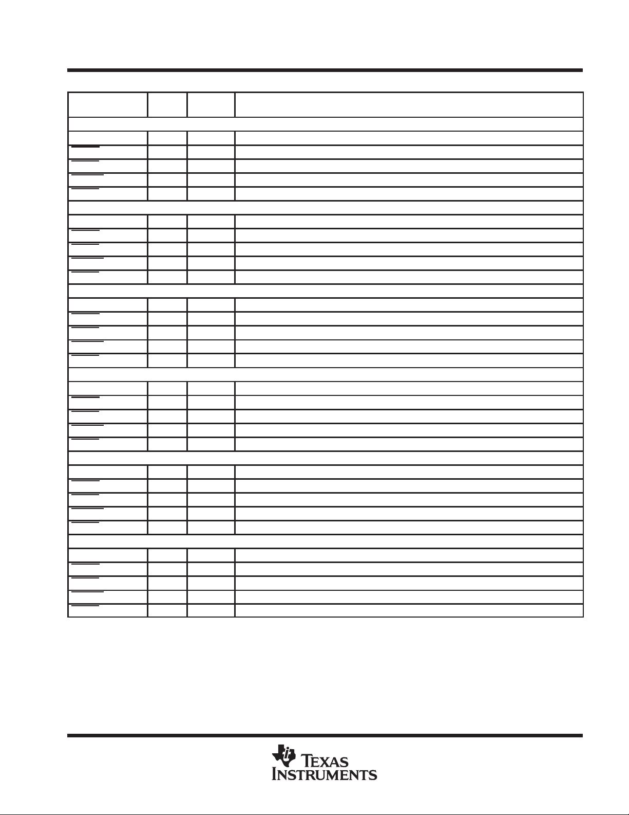
TMS320C40
DIGITAL SIGNAL PROCESSOR
SPRS038 – JANUARY 1996
D
Highest Performance Floating-Point Digital
Signal Processor (DSP)
– ’320C40-60:
33-ns Instruction Cycle Time,
330 MOPS, 60 MFLOPS,
30 MIPS, 384M Bytes/s
– ’320C40-50:
40-ns Instruction Cycle Time
– ’320C40-40:
50-ns Instruction Cycle Time
D
Six Communications Ports
D
Six-Channel Direct Memory Access (DMA)
Coprocessor
D
Single-Cycle Conversion to and From
IEEE-754 Floating-Point Format
D
Single Cycle, 1/x, 1/
D
Source-Code Compatible With TMS320C3x
D
Single-Cycle 40-Bit Floating-Point,
Ǹ
x
32-Bit Integer Multipliers
D
Twelve 40-Bit Registers, Eight Auxiliary
Registers, 14 Control Registers, and Two
Timers
D
IEEE 1149.1† (JT AG) Boundary Scan
Compatible
D
Two Identical External Data and Address
Buses Supporting Shared Memory Systems
and High Data-Rate, Single-Cycle
Transfers:
– High Port-Data Rate of 120M Bytes/s
(’C40-60) (Each Bus)
– 16G-Byte Continuous
Program/Data/Peripheral Address
Space
– Memory-Access Request for Fast,
Intelligent Bus Arbitration
– Separate Address-Bus, Data-Bus, and
Control-Enable Pins
– Four Sets of Memory-Control Signals
Support Different Speed Memories in
Hardware
D
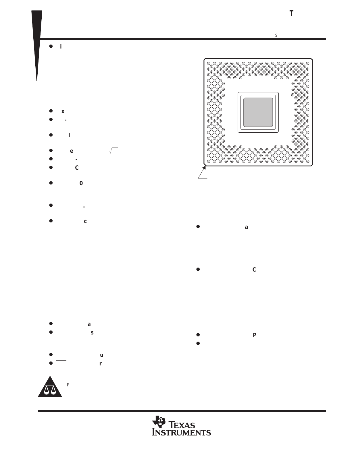
325-Pin Ceramic Grid Array (GF Suffix)
D
Fabricated Using 0.72-µm Enhanced
Performance Implanted CMOS (EPIC)
Technology by Texas Instruments (TI)
D
Software-Communication-Port Reset
D
NMI With Bus-Grant Feature
325-PIN GF GRID ARRAY PACKAGE
AR
AP
AN
AM
AL
AK
AJ
AH
AG
AF
AE
AD
AC
AB
AA
Y
W
V
U
T
R
P
N
M
L
K
J
H
G
F
E
D
C
B
A
123456789
‡
Pin A1
See Pin Assignments table and Pin Functions table for location
and description of all pins.
D
Separate Internal Program, Data, and DMA
(BOTTOM VIEW)
10
14 1617181920212223242526 282730
11 131215
‡
29 3132333435
Coprocessor Buses for Support of Massive
Concurrent Input/Output (I/O) of Program
and Data Throughput, Maximizing
Sustained Central Processing Unit (CPU)
Performance
D
On-Chip Program Cache and
Dual-Access/Single-Cycle RAM for
Increased Memory-Access Performance
– 512-Byte Instruction Cache
– 8K Bytes of Single-Cycle Dual-Access
Program or Data RAM
– ROM-Based Boot Loader Supports
Program Bootup Using 8-, 16-, or 32-Bit
Memories or One of the Communication
Ports
D
IDLE2 Clock-Stop Power-Down Mode
D
5-V Operation
Please be aware that an important notice concerning availability, standard warranty, and use in critical applications of
Texas Instruments semiconductor products and disclaimers thereto appears at the end of this data sheet.
†
IEEE Standard 1149.1–1990 Standard Test-Access Port and Boundary-Scan Architecture
EPIC and TI are trademarks of Texas Instruments Incorporated.
PRODUCTION DATA information is current as of publication date.
Products conform to specifications per the terms of Texas Instruments
standard warranty. Production processing does not necessarily include
testing of all parameters.
POST OFFICE BOX 1443 • HOUSTON, TEXAS 77251–1443
Copyright 1996, Texas Instruments Incorporated
1
TMS320C40
DIGITAL SIGNAL PROCESSOR
SPRS038 – JANUARY 1996
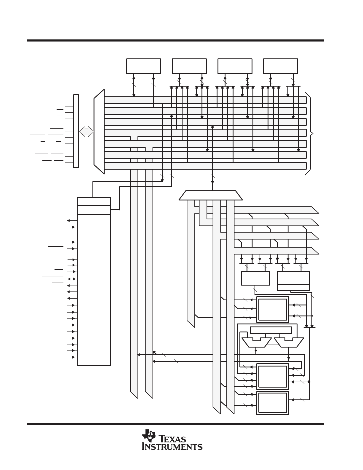
block diagram
D(31–0)
A(30–0)
DE
AE
STAT(3–0)
LOCK
STRB0, STRB1
R/W0, R/W1
PAGE0, PAGE1
, RDY1
RDY0
CE0, CE1
X1
X2/CLKIN
ROMEN
RESET
RESETLOC0
RESETLOC1
NMI
IIOF(3–0)
IACK
H1
H3
CV
SS
DV
DD
DV
SS
IV
SS
LADV
DD
LDDV
DD
V
DDL
V
SSL
SUBS
M
U
X
IR
PC
Controller
Cache
(512 Bytes)
32 32
PDATA Bus
PADDR Bus
DDATA Bus
DADDR 1 Bus
DADDR 2 Bus
DMADATA Bus
DMAADDR Bus
RAM Block 0
(4K Bytes)
32
32 32
32
32
32
RAM Block 1
(4K Bytes)
32
C
P
U
1
MUX
32
R
E
G
1
R
E
G
2
32
40 40
Multiplier
40
40
32
ARAU0 ARAU1
32
32
32
32
32
32
ROM Block
(Reserved)
32
CPU1
CPU2
REG1
REG2
32-Bit Barrel
40
Extended
Precision
Registers
(R0–R11)
DISP, IR0, IR1
BK
Auxiliary
Registers
(AR0–AR7)
Other
Registers
(14)
32
40
Shifter
ALU
32
32
Continued on next page
40
40
40
40
32
32
2
POST OFFICE BOX 1443 • HOUSTON, TEXAS 77251–1443
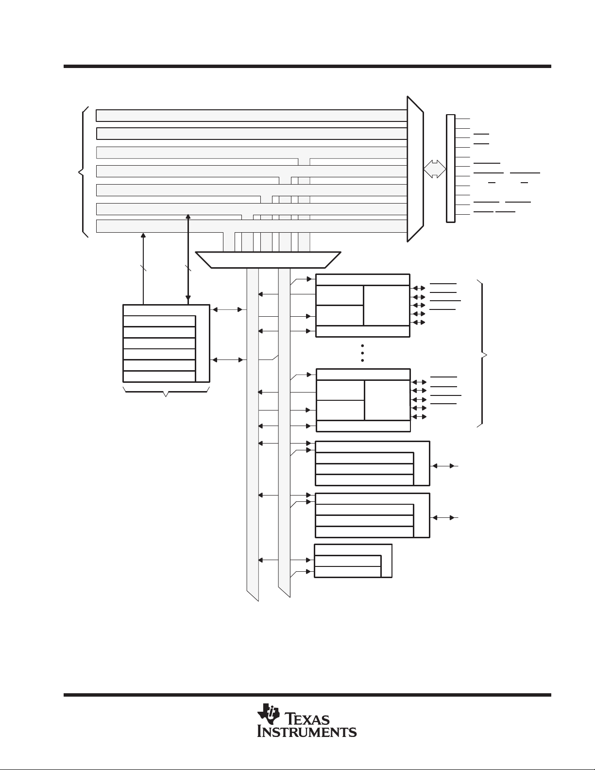
block diagram (continued)
TMS320C40
DIGITAL SIGNAL PROCESSOR
SPRS038 – JANUARY 1996
PDATA Bus
PADDR Bus
DDATA Bus
DADDR 1 Bus
DADDR 2 Bus
DMADATA Bus
Continued from previous page
DMAADDR Bus
3232
DMA Coprocessor
DMA Channel 0
DMA Channel 1
DMA Channel 2
DMA Channel 3
DMA Channel 4
DMA Channel 5
Six DMA Channels
MUX
Peripheral Data Bus
Peripheral Address Bus
Global-Control Register
COM Port 0
Input
FIFO
Output
FIFO
Port-Control Registers
COM Port 5
Input
FIFO
Output
FIFO
Port-Control Registers
Timer 0
Time-Period Register
Timer-Counter Register
PAU
PAU
M
U
X
CREQ0
CACK0
CSTRB0
CRDY0
C0D7–C0D0
CREQ5
CACK5
CSTRB5
CRDY5
C5D7–C5D0
LD31–LD0
LA30–LA0
LDE
LAE
LSTAT3–LSTAT0
LLOCK
LSTRB0–LSTRB1
LR/W0–LR/W1
LPAGE0–LPAGE1
–LRDY1
LRDY0
LCE0,LCE1
Six Communication Ports
TCLK0
Timer 1
Global-Control Register
Time-Period Register
Timer-Counter Register
Port Control
Global
Local
POST OFFICE BOX 1443 • HOUSTON, TEXAS 77251–1443
TCLK1
3
TMS320C40
DIGITAL SIGNAL PROCESSOR
SPRS038 – JANUARY 1996
functions
This section lists signal descriptions for the ’320C40 device. The ’320C40 pin functions table lists each signal,
number of pins, operating mode(s) (that is, input, output, or high-impedance state as indicated by I, O, or Z,
respectively), and function. The signals are grouped according to function.
Pin Functions
NAME
D31–D0 32 I/O/Z 32-bit data port of the global-bus external interface
DE 1 I Data-bus-enable signal for the global-bus external interface
A30–A0 31 O/Z 31-bit address port of the global-bus external interface
AE 1 I Address-bus-enable signal for the global-bus external interface
STAT3–STAT0 4 O Status signals for the global-bus external interface
LOCK 1 O Lock signal for the global-bus external interface
‡
STRB0
‡
R/W0
‡
PAGE0
‡
RDY0
‡
CE0
‡
STRB1
‡
R/W1
‡
PAGE1
‡
RDY1
‡
CE1
LD31–LD0 32 I/O/Z 32-bit data port of the local-bus external interface
LDE 1 I Data-bus-enable signal for the local-bus external interface
LA30–LA0 31 O/Z 31-bit address port of the local-bus external interface
LAE 1 I Address-bus-enable signal for the local-bus external interface
LSTAT3–LSTAT0 4 O Status signals for the local-bus external interface
LLOCK 1 O Lock signal for the local-bus external interface
‡
LSTRB0
LR/W0 1 O/Z Read/write signal for LSTRB0 accesses
LPAGE0 1 O/Z Page signal for LSTRB0 accesses
LRDY0 1 I Ready signal for LSTRB0 accesses
LCE0 1 I Control enable for the LSTRB0, LPAGE0, and LR/W0 signals
‡
LSTRB1
LR/W1 1 O/Z Read/write signal for LSTRB1 accesses
LPAGE1 1 O/Z Page signal for LSTRB1 accesses
LRDY1 1 I Ready signal for LSTRB1 accesses
LCE1 1 I Control enable for the LSTRB1, LPAGE1, and LR/W1 signals
†
I = input, O = output, Z = high impedance
‡
Signal’s effective address range is defined by the local/global STRB ACTIVE bits.
NO. OF
PINS
1 O/Z Access strobe 0 for the global-bus external interface
1 O/Z Read/write signal for STRB0 accesses
1 O/Z Page signal for STRB0 accesses
1 I Ready signal for STRB0 accesses
1 I Control enable for the STRB0, PAGE0, and R/W0 signals
1 O/Z Access strobe 1 for the global-bus external interface
1 O/Z Read/write signal for STRB1 accesses
1 O/Z Page signal for STRB1 accesses
1 I Ready signal for STRB1 accesses
1 I Control enable for the STRB1, PAGE1, and R/W1 signals
1 O/Z Access strobe 0 for the local-bus external interface
1 O/Z Access strobe 1 for the local-bus external interface
TYPE
†
GLOBAL-BUS EXTERNAL INTERFACE (80 PINS)
LOCAL-BUS EXTERNAL INTERFACE (80 PINS)
DESCRIPTION
4
POST OFFICE BOX 1443 • HOUSTON, TEXAS 77251–1443
DIGITAL SIGNAL PROCESSOR
Pin Functions (Continued)
NAME
C0D7–C0D0 8 I/O Communication port 0 data bus
CREQ0 1 I/O Communication port 0 token-request signal
CACK0 1 I/O Communication port 0 token-request-acknowledge signal
CSTRB0 1 I/O Communication port 0 data-strobe signal
CRDY0 1 I/O Communication port 0 data-ready signal
C1D7–C1D0 8 I/O Communication port 1 data bus
CREQ1 1 I/O Communication port 1 token-request signal
CACK1 1 I/O Communication port 1 token-request-acknowledge signal
CSTRB1 1 I/O Communication port 1 data-strobe signal
CRDY1 1 I/O Communication port 1 data-ready signal
C2D7–C2D0 8 I/O Communication port 2 data bus
CREQ2 1 I/O Communication port 2 token-request signal
CACK2 1 I/O Communication port 2 token-request-acknowledge signal
CSTRB2 1 I/O Communication port 2 data-strobe signal
CRDY2 1 I/O Communication port 2 data-ready signal
C3D7–C3D0 8 I/O Communication port 3 data bus
CREQ3 1 I/O Communication port 3 token-request signal
CACK3 1 I/O Communication port 3 token-request-acknowledge signal
CSTRB3 1 I/O Communication port 3 data-strobe signal
CRDY3 1 I/O Communication port 3 data-ready signal
C4D7–C4D0 8 I/O Communication port 4 data bus
CREQ4 1 I/O Communication port 4 token-request signal
CACK4 1 I/O Communication port 4 token-request-acknowledge signal
CSTRB4 1 I/O Communication port 4 data-strobe signal
CRDY4 1 I/O Communication port 4 data-ready signal
C5D7–C5D0 8 I/O Communication port 5 data bus
CREQ5 1 I/O Communication port 5 token-request signal
CACK5 1 I/O Communication port 5 token-request-acknowledge signal
CSTRB5 1 I/O Communication port 5 data-strobe signal
CRDY5 1 I/O Communication port 5 data-ready signal
†
I = input, O = output, Z = high impedance
NO. OF
PINS
TYPE
†
COMMUNICATION PORT 0 INTERFACE (12 PINS)
COMMUNICATION PORT 1 INTERFACE (12 PINS)
COMMUNICATION PORT 2 INTERFACE (12 PINS)
COMMUNICATION PORT 3 INTERFACE (12 PINS)
COMMUNICATION PORT 4 INTERFACE (12 PINS)
COMMUNICATION PORT 5 INTERFACE (12 PINS)
DESCRIPTION
TMS320C40
SPRS038 – JANUARY 1996
POST OFFICE BOX 1443 • HOUSTON, TEXAS 77251–1443
5
TMS320C40
DIGITAL SIGNAL PROCESSOR
SPRS038 – JANUARY 1996
Pin Functions (Continued)
NAME
IIOF3–IIOF0 4 I/O Interrupt and I/O flags
NMI 1 I Nonmaskable interrupt. NMI is sensitive to a low-going edge.
IACK 1 O Interrupt acknowledge
RESET 1 I Reset signal
RESETLOC1–
RESETLOC0
ROMEN 1 I On-chip ROM enable (0 = disable, 1 = enable)
TCLK0 1 I/O Timer 0 pin
TCLK1 1 I/O Timer 1 pin
X1 1 O Crystal pin
X2/CLKIN 1 I Crystal/oscillator pin
H1 1 O H1 clock
H3 1 O H3 clock
CV
SS
DV
SS
IV
SS
DV
DD
GADV
DD
GDDV
DD
LADV
DD
LDDV
DD
SUBS 1 I Substrate pin (tie to ground)
V
DDL
V
SSL
TCK 1 I IEEE 1149.1 test port clock
TDO 1 O/Z IEEE 1149.1 test port data out
TDI 1 I IEEE 1149.1 test port data in
TMS 1 I IEEE 1149.1 test port mode select
TRST 1 I IEEE 1149.1 test port reset
EMU0 1 I/O Emulation pin 0
EMU1 1 I/O Emulation pin 1
†
I = input, O = output, Z = high impedance
NO. OF
PINS
2 I Reset-vector location pins
15 I Ground pins
15 I Ground pins
6 I Ground pins
13 I 5-VDC supply pins
3 I 5-VDC supply pins
3 I 5-VDC supply pins
3 I 5-VDC supply pins
3 I 5-VDC supply pins
4 I 5-VDC supply pins
4 I Ground pins
†
TYPE
INTERRUPTS, I/O FLAGS, RESET, TIMER ( 12 PINS)
CLOCK (4 PINS)
POWER (70 PINS)
EMULATION (7 PINS)
DESCRIPTION
6
POST OFFICE BOX 1443 • HOUSTON, TEXAS 77251–1443
TMS320C40
DIGITAL SIGNAL PROCESSOR
SPRS038 – JANUARY 1996
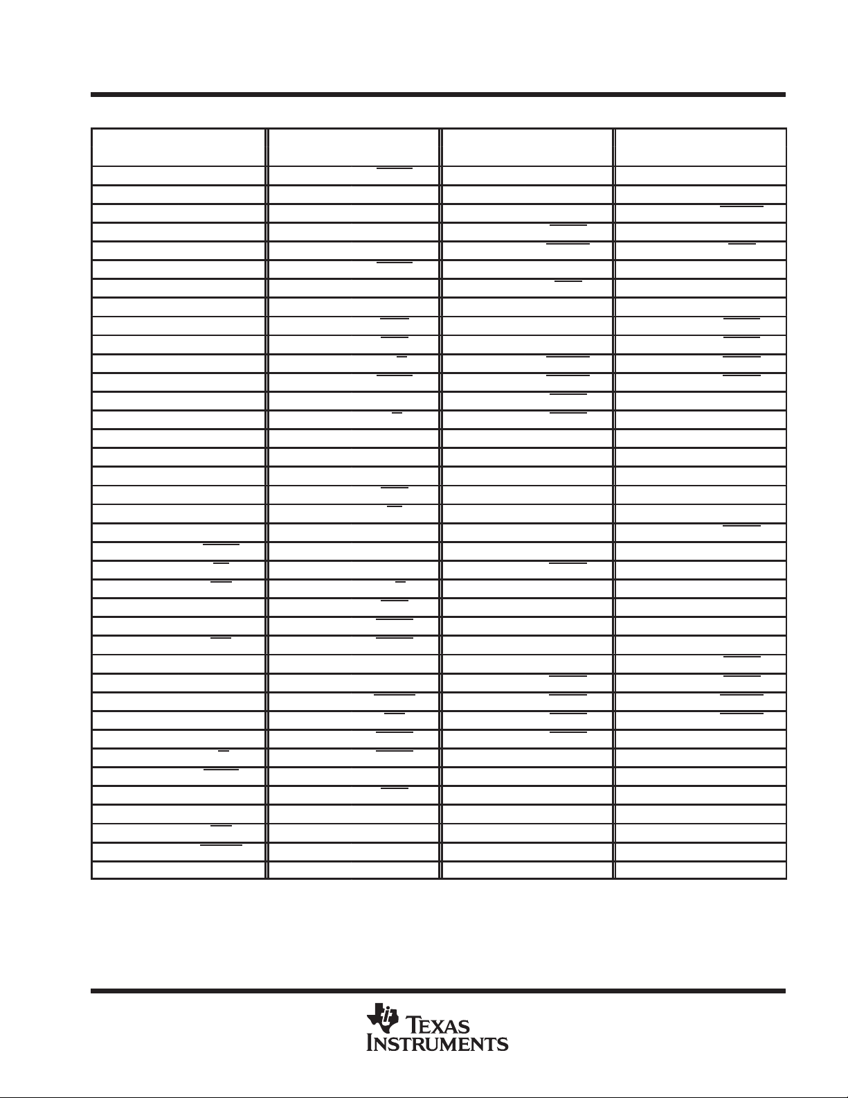
GF Package Pin Assignments — Alphabetical Listing
PIN PIN PIN PIN PIN
NAME NO. NAME NO. NAME NO. NAME NO. NAME NO.
A0 D32 C0D6 AN7 C5D4 AM30 CV
A1 B32 C0D7 AK8 C5D5 AP32 CV
A2 D30 C1D0 AL7 C5D6 AM32 CV
A3 C29 C1D1 AP8 C5D7 AL31 CV
A4 B30 C1D2 AM8 CACK0 AN11 CV
A5 F28 C1D3 AK12 CACK1 AN13 CV
A6 F24 C1D4 AK10 CACK2 AM14 CV
A7 E29 C1D5 AN9 CACK3 AM16 D0 U33 DV
A8 C27 C1D6 AL9 CACK4 AK32 D1 V32 DV
A9 D28 C1D7 AP10 CACK5 AJ31 D2 T34 DV
A10 B28 C2D0 AM18 CE0 AA33 D3 U31 DV
A11 F26 C2D1 AN19 CE1 V34 D4 R33 DV
A12 C25 C2D2 AL19 CRDY0 AP12 D5 P34 DV
A13 E27 C2D3 AP20 CRDY1 AP14 D6 T32 DV
A14 B26 C2D4 AM20 CRDY2 AL15 D7 N33 DV
A15 D26 C2D5 AN21 CRDY3 AL17 D8 R31 DV
A16 C23 C2D6 AL21 CRDY4 AH30 D9 M34 DV
A17 B24 C2D7 AP22 CRDY5 AH32 D10 P32 DV
A18 E25 C3D0 AM22 CREQ0 AM10 D11 L33 DV
A19 C21 C3D1 AN23 CREQ1 AM12 D12 N31 DV
A20 D24 C3D2 AL23 CREQ2 AN15 D13 K34 DV
A21 B22 C3D3 AP24 CREQ3 AN17 D14 M32 DV
A22 E23 C3D4 AM24 CREQ4 AN33 D15 J33 DV
A23 C19 C3D5 AN25 CREQ5 AL33 D16 L31 DV
A24 D22 C3D6 AL25 CSTRB0 AL11 D17 M30 DV
A25 B20 C3D7 AP26 CSTRB1 AL13 D18 K32 DV
A26 E21 C4D0 AN27 CSTRB2 AP16 D19 H34 DV
A27 B18 C4D1 AM26 CSTRB3 AP18 D20 J31 DV
A28 C17 C4D2 AK24 CSTRB4 AM34 D21 G33 DV
A29 D20 C4D3 AL27 CSTRB5 AK34 D22 K30 DV
A30 B16 C4D4 AP28 CV
AE AG31 C4D5 AK26 CV
C0D0 AP4 C4D6 AN29 CV
C0D1 AL5 C4D7 AM28 CV
C0D2 AN5 C5D0 AL29 CV
C0D3 AM4 C5D1 AP30 CV
C0D4 AP6 C5D2 AK28 CV
C0D5 AM6 C5D3 AN31 CV
SS
SS
SS
SS
SS
SS
SS
SS
AR19 D23 F34 EMU0 AA35
AR7 D24 H32 EMU1 AD34
N1 D25 E33 GADV
AL35 D26 D34 GADV
A27 D27 G31 GADV
A9 D28 C33 GDDV
E1 D29 H30 GDDV
J35 D30 E31 GDDV
SS
SS
SS
SS
SS
SS
SS
E35 D31 F32
AR25 DE AA31
AE1 DV
AR13 DV
A19 DV
R35 DV
AL1 DV
DD
DD
DD
DD
DD
DD
DD
DD
DD
DD
DD
DD
DD
SS
SS
SS
SS
SS
SS
SS
SS
SS
SS
SS
SS
SS
SS
SS
DD
DD
DD
DD
DD
DD
AR11
AR29
A13
A7
A17
L35
AR23
A29
L1
AC1
AR17
A23
AJ1
AJ35
A21
A25
G35
A11
AG1
AM2
R1
AR21
AR15
A15
AR27
G1
N35
AR9
B2
AR1
U35
V2
A35
A1
POST OFFICE BOX 1443 • HOUSTON, TEXAS 77251–1443
7
TMS320C40
DIGITAL SIGNAL PROCESSOR
SPRS038 – JANUARY 1996
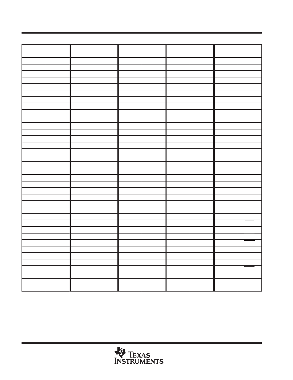
GF Package Pin Assignments — Alphabetical Listing (Continued)
PIN PIN PIN PIN
NAME NO. NAME NO. NAME NO. NAME NO.
H1 AC3 LA25 R5 LD26 B4 STAT0 AD32
H3 AC5 LA26 T2 LD27 F8 STAT1 AE33
IACK W3 LA27 U3 LD28 D6 STAT2 AF34
IIOF0 AN3 LA28 T4 LD29 C3 STAT3 AE31
IIOF1 AL3 LA29 V4 LD30 E5 STRB0 AD30
IIOF2 AH6 LA30 U5 LD31 F6 STRB1 AC33
IIOF3 AK2 LADV
IV
SS
IV
SS
IV
SS
IV
SS
IV
SS
IV
SS
LA0 D2 LD1 C15 LPAGE1 AG3 TRST AE35
LA1 D4 LD2 D18 LRDY0 AF6 V
LA2 E3 LD3 B14 LRDY1 AE5 V
LA3 F4 LD4 E17 LR/W0 AH4 V
LA4 H6 LD5 D16 LR/W1 AF4 V
LA5 F2 LD6 C13 LSTAT0 AA3 V
LA6 G5 LD7 E15 LSTAT1 Y4 V
LA7 G3 LD8 B12 LSTAT2 Y2 V
LA8 H4 LD9 D14 LSTAT3 W5 V
LA9 H2 LD10 C11 LSTRB0 AJ3 X1 W1
LA10 K6 LD11 E13 LSTRB1 AD6 X2/CLKIN AA1
LA11 M6 LD12 B10 NMI AJ5
LA12 J5 LD13 D12 PAGE0 AG33
LA13 J3 LD14 C9 PAGE1 AB32
LA14 K4 LD15 E11 RDY0 Y32
LA15 K2 LD16 F12 RDY1 W31
LA16 L3 LD17 D10 RESETLOC0 AF30
LA17 L5 LD18 B8 RESETLOC1 AH34
LA18 M2 LD19 E9 RESET AJ33
LA19 M4 LD20 C7 ROMEN AK4
LA20 N3 LD21 F10 R/W0 AF32
LA21 N5 LD22 B6 R/W1 AC31
LA22 P2 LD23 D8
LA23 P4 LD24 C5
LA24 R3 LD25 E7
AR5 LADV
AR31 LADV
AG35 LAE AB4 LDE AD4 TCLK1 AD2
A31 LCE0 AG5 LLOCK AA5 TDO AB34
J1 LCE1 AF2 LOCK W33 TDI AC35
A5 LD0 E19 LPAGE0 AH2 TMS W35
DD
DD
DD
B34 LDDV
AB2 LDDV
AP34 LDDV
DD
DD
DD
AR35 SUBS C31
AP2 TCK Y34
U1 TCLK0 AE3
DDL
DDL
DDL
DDL
SSL
SSL
SSL
SSL
AN1
AN35
C35
C1
A3
AR3
AR33
A33
8
POST OFFICE BOX 1443 • HOUSTON, TEXAS 77251–1443
DIGITAL SIGNAL PROCESSOR
SPRS038 – JANUARY 1996
GF Package Pin Assignments — Numerical Listing
PIN PIN PIN PIN
NO. NAME NO. NAME NO. NAME NO. NAME
A1 GDDV
A3 V
A5 IV
A7 DV
A9 CV
A11 DV
A13 DV
A15 DV
A17 DV
A19 CV
A21 DV
A23 DV
A25 DV
A27 CV
A29 DV
A31 IV
A33 V
A35 GDDV
AA1 X2/CLKIN AG31 AE AL27 C4D3 AN31 C5D3
AA3 LSTAT0 AG33 PAGE0 AL29 C5D0 AN33 CREQ4
AA5 LLOCK AG35 IV
AA31 DE AH2 LPAGE0 AL33 CREQ5 AP2 LDDV
AA33 CE0 AH4 LR/W0 AL35 CV
AA35 EMU0 AH6 IIOF2 AM2 DV
AB2 LADV
AB4 LAE AH32 CRDY5 AM6 C0D5 AP10 C1D7
AB32 PAGE1 AH34 RESETLOC1 AM8 C1D2 AP12 CRDY0
AB34 TDO AJ1 DV
AC1 DV
AC3 H1 AJ5 NMI AM14 CACK2 AP18 CSTRB3
AC5 H3 AJ31 CACK5 AM16 CACK3 AP20 C2D3
AC31 R/W1 AJ33 RESET AM18 C2D0 AP22 C2D7
AC33 STRB1 AJ35 DV
AC35 TDI AK2 IIOF3 AM22 C3D0 AP26 C3D7
AD2 TCLK1 AK4 ROMEN AM24 C3D4 AP28 C4D4
AD4 LDE AK8 C0D7 AM26 C4D1 AP30 C5D1
AD6 LSTRB1 AK10 C1D4 AM28 C4D7 AP32 C5D5
DD
SSL
SS
DD
SS
SS
DD
SS
DD
SS
SS
DD
SS
SS
DD
SS
SSL
DD
DD
DD
AD30 STRB0 AK24 C4D2 AM30 C5D4
AD32 STAT0 AK26 C4D5 AM32 C5D6
AD34 EMU1 AK28 C5D2 AM34 CSTRB4
AE1 CV
AE3 TCLK0 AK34 CSTRB5 AN3 IIOF0
AE5 LRDY1 AL1 CV
AE31 STAT3 AL3 IIOF1 AN7 C0D6
AE33 STAT1 AL5 C0D1 AN9 C1D5
AE35 TRST AL7 C1D0 AN11 CACK0
AF2 LCE1 AL9 C1D6 AN13 CACK1
AF4 LR/W1 AL11 CSTRB0 AN15 CREQ2
AF6 LRDY0 AL13 CSTRB1 AN17 CREQ3
AF30 RESETLOC0 AL15 CRDY2 AN19 C2D1
AF32 R/W0 AL17 CRDY3 AN21 C2D5
AF34 STAT2 AL19 C2D2 AN23 C3D1
AG1 DV
AG3 LPAGE1 AL23 C3D2 AN27 C4D0
AG5 LCE0 AL25 C3D6 AN29 C4D6
AH30 CRDY4 AM4 C0D3 AP8 C1D1
AJ3 LSTRB0 AM12 CREQ1 AP16 CSTRB2
AK12 C1D3 AP34 LADV
SS
SS
SS
DD
SS
AK32 CACK4 AN1 V
SS
AL21 C2D6 AN25 C3D5
AL31 C5D7 AN35 V
SS
SS
AM10 CREQ0 AP14 CRDY1
AM20 C2D4 AP24 C3D3
AN5 C0D2
AP4 C0D0
AP6 C0D4
TMS320C40
DDL
DDL
DD
DD
POST OFFICE BOX 1443 • HOUSTON, TEXAS 77251–1443
9
TMS320C40
DIGITAL SIGNAL PROCESSOR
SPRS038 – JANUARY 1996
GF Package Pin Assignments — Numerical Listing (Continued)
PIN PIN PIN PIN PIN
NO. NAME NO. NAME NO. NAME NO. NAME NO. NAME
AR1 GADV
AR3 V
AR5 IV
AR7 CV
AR9 DV
AR11 DV
AR13 CV
AR15 DV
AR17 DV
AR19 CV
AR21 DV
AR23 DV
AR25 CV
AR27 DV
AR29 DV
AR31 IV
AR33 V
AR35 LDDV
B2 GADV
B4 LD26 D4 LA1 F4 LA3 L3 LA16 U35 GADV
B6 LD22 D6 LD28 F6 LD31 L5 LA17 V2 GDDV
B8 LD18 D8 LD23 F8 LD27 L31 D16 V4 LA29
B10 LD12 D10 LD17 F10 LD21 L33 D11 V32 D1
B12 LD8 D12 LD13 F12 LD16 L35 DV
B14 LD3 D14 LD9 F24 A6 M2 LA18 W1 X1
B16 A30 D16 LD5 F26 A11 M4 LA19 W3 IACK
B18 A27 D18 LD2 F28 A5 M6 LA11 W5 LSTAT3
B20 A25 D20 A29 F32 D31 M30 D17 W31 RDY1
B22 A21 D22 A24 F34 D23 M32 D14 W33 LOCK
B24 A17 D24 A20 G1 DV
B26 A14 D26 A15 G3 LA7 N1 CV
B28 A10 D28 A9 G5 LA6 N3 LA20 Y4 LSTAT1
B30 A4 D30 A2 G31 D27 N5 LA21 Y32 RDY0
B32 A1 D32 A0 G33 D21 N31 D12 Y34 TCK
B34 LADV
DD
SSL
SS
SS
SS
DD
SS
SS
DD
SS
SS
DD
SS
SS
DD
SS
SSL
DD
DD
DD
C1 V
C3 LD29 E3 LA2 H4 LA8 P4 LA23
C5 LD24 E5 LD30 H6 LA4 P32 D10
C7 LD20 E7 LD25 H30 D29 P34 D5
C9 LD14 E9 LD19 H32 D24 R1 DV
C11 LD10 E11 LD15 H34 D19 R3 LA24
C13 LD6 E13 LD11 J1 IV
C15 LD1 E15 LD7 J3 LA13 R31 D8
C17 A28 E17 LD4 J5 LA12 R33 D4
C19 A23 E19 LD0 J31 D20 R35 CV
C21 A19 E21 A26 J33 D15 T2 LA26
C23 A16 E23 A22 J35 CV
C25 A12 E25 A18 K2 LA15 T32 D6
C27 A8 E27 A13 K4 LA14 T34 D2
C29 A3 E29 A7 K6 LA10 U1 LDDV
C31 SUBS E31 D30 K30 D22 U3 LA27
C33 D28 E33 D25 K32 D18 U5 LA30
C35 V
D2 LA0 F2 LA5 L1 DV
D34 D26 G35 DV
DDL
DDL
E1 CV
E35 CV
SS
SS
SS
SS
H2 LA9 P2 LA22
SS
SS
K34 D13 U31 D3
DD
DD
M34 D9 W35 TMS
SS
N33 D7
N35 DV
SS
R5 LA25
T4 LA28
U33 D0
V34 CE1
Y2 LSTAT2
SS
SS
DD
DD
DD
10
POST OFFICE BOX 1443 • HOUSTON, TEXAS 77251–1443
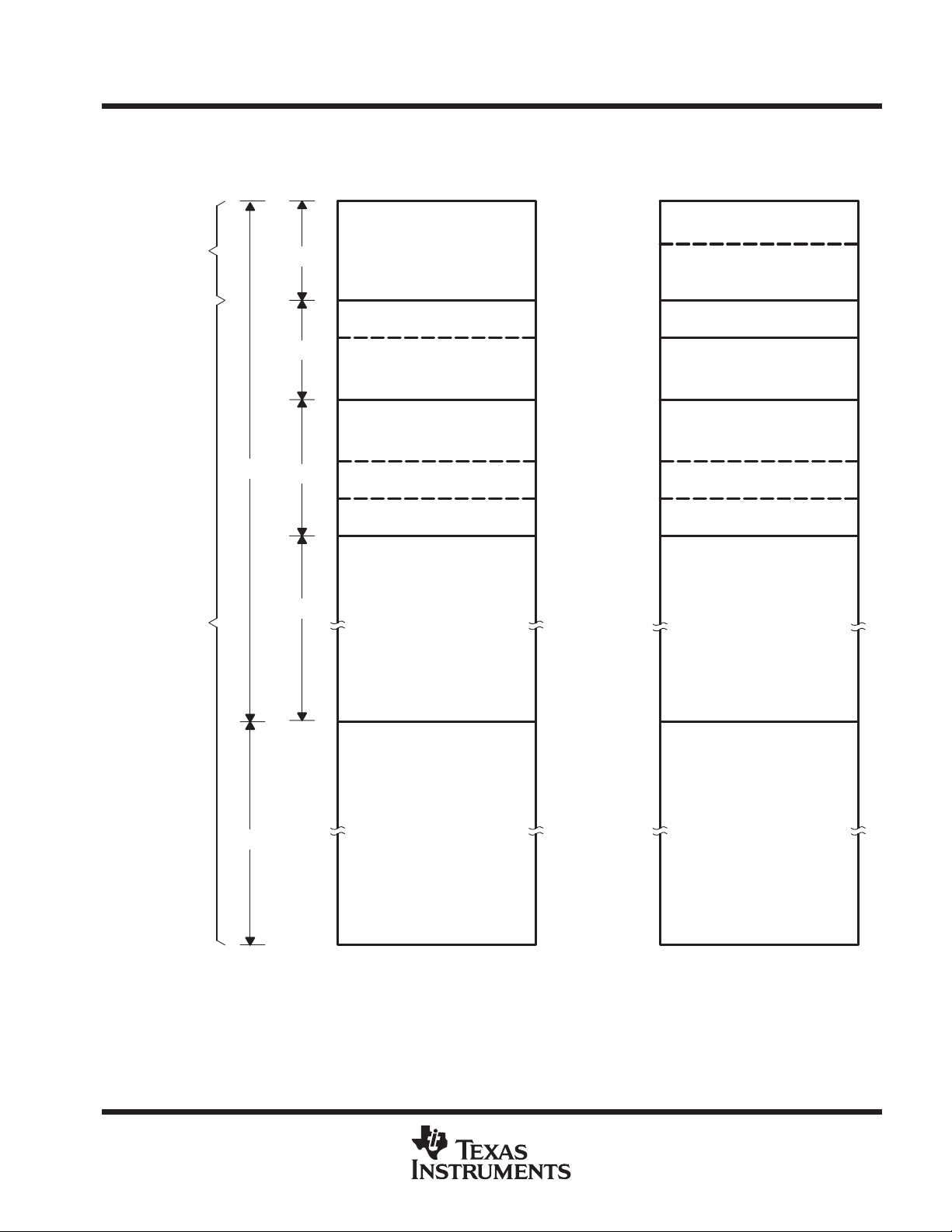
memory map
TMS320C40
DIGITAL SIGNAL PROCESSOR
SPRS038 – JANUARY 1996
Figure 1 shows the memory map for the ’320C40. Refer to the
SPRU063B) for a detailed description of this memory mapping.
Structure
Depends
Upon
ROMEN Bit
Structure
Identical
2G
1M
1M
1M
2G–3M
Accessible Local Bus
(External)
Peripherals (Internal)
Reserved
Reserved
1K RAM BLK 0 (Internal)
1K RAM BLK 1 (Internal)
Local Bus
(External)
TMS320C4x User’s Guide
000000000h
000000FFFh
000001000h
0000FFFFFh
000100000h
0001000FFh
000100100h
0001FFFFFh
000200000h
0002FF7FFh
0002FF800h
0002FFBFFh
0002FFC00h
0002FFFFFh
000300000h
Boot-Loader ROM
Peripherals (Internal)
1K RAM BLK 0 (Internal)
1K RAM BLK 1 (Internal)
(literature number
(Internal)
Reserved
Reserved
Reserved
Local Bus
(External)
2G
07FFFFFFFh
080000000h
Global Bus (External)
0FFFFFFFFh
(a) Internal ROM Disabled
(ROMEN = 0)
Microprocessor Mode
Figure 1. Memory Map for ’320C40
Global Bus (External)
(b) Internal ROM Enabled
(ROMEN = 1)
Microcomputer Mode
POST OFFICE BOX 1443 • HOUSTON, TEXAS 77251–1443
11

TMS320C40
DIGITAL SIGNAL PROCESSOR
SPRS038 – JANUARY 1996
description
The ’320C40 digital signal processors (DSPs) are 32-bit, floating-point processors manufactured in 0.72-µm,
double-level metal CMOS technology. The ’320C40 is a part of the fourth generation of DSPs from Texas
Instruments and is designed primarily for parallel processing.
operation
The ’320C40 has six on-chip communication ports for processor-to-processor communication with no external
hardware and simple communication software. This allows connectivity to other ’C4x processors with no
external-glue logic. The communication ports remove input / output bottlenecks, and the independent smart
DMA coprocessor is able to handle the CPU input/output burden.
central processing unit
The ’320C40 CPU is configured for high-speed internal parallelism for the highest sustained performance. The
key features of the CPU are:
D
Eight operations/cycle:
– 40/32-bit floating-point/integer multiply
– 40/32-bit floating-point/integer ALU operation
– Two data accesses
– Two address register updates
D
IEEE floating-point conversion
D
Divide and square-root support
D
’C3x assembly language compatibility
D
Byte and halfword accessibility
DMA coprocessor
The DMA coprocessor allows concurrent I/O and CPU processing for the highest sustained CPU performance.
The key features of the DMA processor are:
D
Link pointers allow DMA channels to auto-initialize without CPU intervention.
D
Parallel CPU operation and DMA transfers
D
Six DMA channels support memory-to-memory data transfers.
D
Split-mode operation doubles the available DMA channel to 12 when data transfers to and from a
communication port are required.
communication ports
The ’320C40 is the first DSP with on-chip communication ports for processor-to-processor communication with
no external hardware and simple communication software. The features of the communication ports are:
D
Direct interprocessor communication and processor I/O
12
D
Six communication ports for direct interprocessor communication and processor I/O
D
20M-bytes/s bidirectional interface on each communication port for high-speed multiprocessor interface
D
Separate input and output 8-word-deep FIFO buffers for processor-to-processor communication and I/O
D
Automatic arbitration and handshaking for direct processor-to-processor connection
POST OFFICE BOX 1443 • HOUSTON, TEXAS 77251–1443
TMS320C40
DIGITAL SIGNAL PROCESSOR
SPRS038 – JANUARY 1996
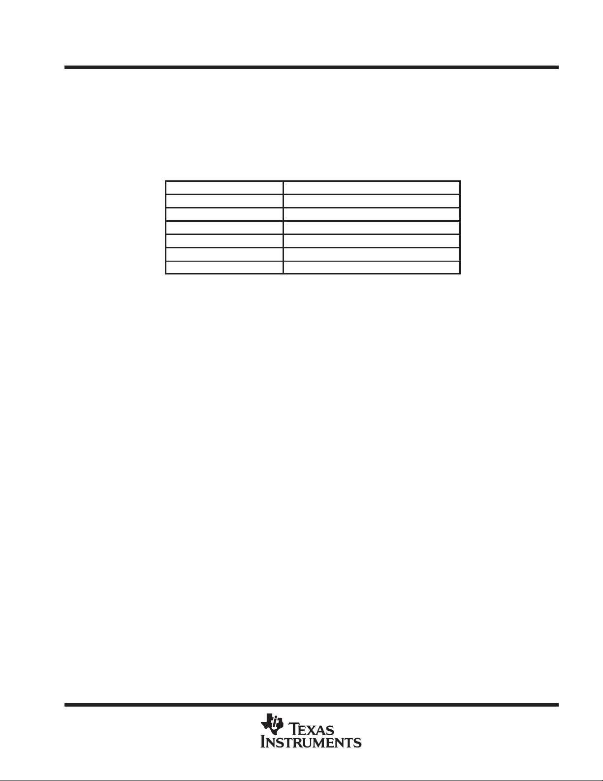
communication-port software reset (’C40 silicon revision ≥ 5.0)
The input and output FIFO levels for a communication port can be flushed by writing at least two back-to-back
values to its communication-port-software reset address as specified in Table 1. This feature is not present in
’C40 silicon revision <5.0. This software reset flushes any word or byte already present in the FIFOs but it does
not affect the status of the communication-port pins. Figure 2 shows an example of
communication-port-software reset.
Table 1. Communication-Port Software-Reset Address
COMMUNICATION PORT SOFTWARE RESET ADDRESS
0 0x0100043
1 0x0100053
2 0x0100063
3 0x0100073
4 0x0100083
5 0x0100093
; –––––––––––––––––––––––––––––––––––––––––––––-–––;
; RESET1:Flush’s FIFO data for communication port 1;
; –––––––––––––––––––––––––––––––––––––––––––––-–––;
RESET1 push AR0 ; Save registers
push R0 ;
push RC ;
ldhi 010h,AR0 ; Set AR0 to base address of COM 1
or 050h,AR0 ;
flush: rpts 1 ; Flush FIFO data with back-to-back write
sti R0,*+AR0(3) ;
rpts 10 ; Wait
nop ;
ldi *+AR0(0),R0 ; Check for new data from other port
and 01FE0h,R0 ;
bnz flush ;
pop RC ; Restore registers
pop R0 ;
pop AR0 ;
rets ; Return
Figure 2. Example of Communication-Port-Software Reset
POST OFFICE BOX 1443 • HOUSTON, TEXAS 77251–1443
13

TMS320C40
DIGITAL SIGNAL PROCESSOR
SPRS038 – JANUARY 1996
NMI with bus-grant feature (’C40 silicon revision ≥ 5.0)
The ’320C40 devices have a software-configurable feature which allows forcing the internal-peripheral bus to
ready when the NMI signal is asserted. This feature is not present in ’C40 silicon revision < 5.0. The NMI
bus-grant feature is enabled when bits 19 – 18 of the status register (ST) are set to 10b. When enabled, a
peripheral bus-grant signal is generated on the falling edge of NMI. When NMI is asserted and this feature is
not enabled, the CPU stalls on access to the peripheral bus if it is not ready . A stall condition occurs when writing
to a full FIFO or reading an empty FIFO. This feature is useful in correcting communication-port errors when
used in conjunction with the communication-port software-reset feature.
IDLE2 clock-stop power-down mode (’C40 silicon revision ≥ 5.0)
The ’320C40 has a clock-stop mode or power-down mode (IDLE2) to achieve extremely low-power
consumption. When an IDLE2 instruction is executed, the clocks are halted with H1 being held high. To exit
IDLE2, assert one of the IIOF3–IIOF0 pins configured as an external interrupt instead of a general-purpose I/O.
A macro showing how to generate the IDLE2 opcode is given in Figure 3. During this power-down mode:
D
No instructions are executed.
D
The CPU, peripherals, and internal memory retain their previous state.
D
The external-bus outputs are idle. The address lines remain in their previous state, the data lines are in
the high-impedance state, and the output-control signals are inactive.
; ––––––––––––––––––––––––––––––––––––––––––––-–-–;
; IDLE2: Macro to generate idle2 opcode ;
; –––––––––––––––––––––––––––––––––––––––––––––-––;
IDLE2 .macro
.word 06000001h
.endm
Figure 3. Example of Software Subroutine Using IDLE2
IDLE2 is exited when one of the five external interrupts (NMI and IIOF3–IIOF0) is asserted low for at least four
input clocks (two H1 cycles). The clocks then start after a delay of two input clocks (one H1 cycle). The clocks
can start in the opposite phase; that is, H1 can be high when H3 was high before the clocks were stopped.
However, the H1 and H3 clocks remain 180° out of phase with each other.
During IDLE2 operation, an external interrupt can be recognized and serviced by the CPU if it is enabled before
entering IDLE2 and asserted for at least two H1 cycles. For the processor to recognize only one interrupt, the
interrupt pin must be configured for edge-trigger mode or asserted less than three cycles in level-trigger mode.
Any external interrupt pin can wake up the device from IDLE2, but for the CPU to recognize that interrupt, it must
also be enabled. If an interrupt is recognized and executed by the CPU, the instruction following the IDLE2
instruction is not executed until after execution of a return opcode.
When the device is in emulation mode, the CPU executes an IDLE2 instruction as if it were an IDLE instruction.
The clocks continue to run for correct operation of the emulator.
14
POST OFFICE BOX 1443 • HOUSTON, TEXAS 77251–1443

TMS320C40
DIGITAL SIGNAL PROCESSOR
SPRS038 – JANUARY 1996
development tools
The ’C40 is supported by a host of parallel-processing development tools for developing and simulating code
easily and for debugging parallel-processing systems. The code generation tools include:
D
An ANSI C compiler optimized with a runtime support library that supports use of communication ports and
DMA.
D
Third party support for C, C++ and Ada compilers
D
Several operating systems available for parallel-processing support, as well as DMA and communication
port drivers
D
An assembler and linker with support for mapping program and data to parallel processors
The simulation tools include:
D
Parallel DSP system-level simulation with LAI hardware verification (HV) model and full function (FF) model.
D
TI software simulator with high-level language debugger interface for simulating a single processor.
The hardware development and verification tools include:
D
Parallel processor in-circuit emulator and high-level language debugger: XDS510.
D
Parallel processor development system (PPDS) with four ’320C40s, local and global memory, and
communication port connections.
silicon revision identification
TMS320C40GFL
EA XXX
YYYYY
@1991 TI TAIWAN
DSP
Device Type
Revision Number and Package Data Code
E XXXXX: Silicon rev 1.X
EA XXXXX: Silicon rev 2.X
EB XXXXX: Silicon rev 3.X
ED XXXXX: Silicon rev 5.x
Lot Number (May or may not exist)
POST OFFICE BOX 1443 • HOUSTON, TEXAS 77251–1443
15

TMS320C40
VIHHigh-level input voltage
V
CC
y
(See Note 4)
DIGITAL SIGNAL PROCESSOR
SPRS038 – JANUARY 1996
absolute maximum ratings over specified temperature range (unless otherwise noted)
†
Supply voltage range, VDD (see Note 1) – 0.3 V to 7 V. . . . . . . . . . . . . . . . . . . . . . . . . . . . . . . . . . . . . . . . . . . . .
Voltage range on any pin – 0.3 V to 7 V. . . . . . . . . . . . . . . . . . . . . . . . . . . . . . . . . . . . . . . . . . . . . . . . . . . . . . . . . .
Output voltage range – 0.3 V to 7 V. . . . . . . . . . . . . . . . . . . . . . . . . . . . . . . . . . . . . . . . . . . . . . . . . . . . . . . . . . . . . .
Operating case temperature range, TC 0°C to 85°C. . . . . . . . . . . . . . . . . . . . . . . . . . . . . . . . . . . . . . . . . . . . . . . .
Storage temperature range, T
†
Stresses beyond those listed under “absolute maximum ratings” may cause permanent damage to the device. These are stress ratings only, and
functional operation of the device at these or any other conditions beyond those indicated under “recommended operating conditions” is not
implied. Exposure to absolute-maximum-rated conditions for extended periods may affect device reliability.
NOTE 1: All voltage values are with respect to VSS.
– 55°C to 150°C. . . . . . . . . . . . . . . . . . . . . . . . . . . . . . . . . . . . . . . . . . . . . . . . . .
stg
recommended operating conditions (see Note 2)
MIN TYP
V
Supply voltages (DDVDD, etc.) 4.75 5 5.25 V
DD
p
V
Low-level input voltage – 0.3
IL
I
High-level output current – 300 µA
OH
I
Low-level output current 2 mA
OL
T
Operating case temperature 85 °C
C
‡
All typical values are at VDD = 5 V, TA (ambient air temperature)= 25°C.
§
This parameter is characterized but not tested.
NOTE 2: All input and output voltage levels are TTL compatible, except for CLKIN. CLKIN can be driven by CMOS clock.
X2/CLKIN 2.6 VDD + 0.3
All other pins 2 VDD + 0.3
§
‡
MAX UNIT
§
§
0.8 V
electrical characteristics over recommended ranges of supply voltage and operating case
temperature (unless otherwise noted)
PARAMETER TEST CONDITIONS MIN TYP¶MAX UNIT
V
High-level output voltage VDD = MIN, IOH = MAX 2.4 3
OH
V
Low-level output voltage VDD = MIN, IOL = MAX 0.3 0.6
OL
I
Three-state current VDD = MAX –20 20
Z
I
Input current, X2/CLKIN only VI = VSS to V
IC
I
Input current
IP
I
Input current VI = VSS to V
I
I
Supply current
C
Input capacitance 15
I
C
Output capacitance 15
O
¶
All typical values are at VDD = 5 V, TA (ambient air temperature) = 25°C.
#
This parameter is specified by design but not tested.
NOTES: 3. Pins with internal pullup devices: TDI, TCK, TMS. Pin with internal pulldown device: TRST
4. fx is the input clock frequency. The maximum value (max) for the ’320C40-40, ’320C40-50, and ’320C40-60 is 40, 50 and 60 MHz,
respectively.
Inputs with internal pullups
(See Note 3)
TA = 25°C, VDD = MAX, fx = MAX
DD
DD
’320C40-40
’320C40-50
’320C40-60 950
– 30 30
–400 20
–10 10
.
350
850
V
V
µA
µA
µA
µA
mA
#
pF
#
pF
16
POST OFFICE BOX 1443 • HOUSTON, TEXAS 77251–1443

TMS320C40
DIGITAL SIGNAL PROCESSOR
SPRS038 – JANUARY 1996
PARAMETER MEASUREMENT INFORMATION
I
OL
Output
Under
Test
Where: I
Tester Pin
Electronics
= 2 mA (all outputs)
OL
= 300 µA (all outputs)
I
OH
V
= 2.15 V
Load
= 80 pF typical load circuit capacitance.
C
T
V
Load
I
OH
C
T
Figure 4. Test Load Circuit
signal transition levels
TTL-level outputs are driven to a minimum logic-high level of 2.4 V and to a maximum logic-low level of 0.6 V .
Output transition times are specified as follows.
For a high-to-low transition on a TTL-compatible output signal, the level at which the output is said to be no
longer high is 2 V and the level at which the output is said to be low is 1 V . For a low-to-high transition, the level
at which the output is said to be no longer low is 1 V and the level at which the output is said to be high is 2 V.
See Figure 5.
2.4 V
2 V
1 V
0.6 V
Figure 5. TTL-Level Outputs
Transition times for TTL-compatible inputs are specified as follows. For a high-to-low transition on an input
signal, the level at which the input is said to be no longer high is 2 V and the level at which the input is said to
be low is 0.8 V . For a low-to-high transition on an input signal, the level at which the input is said to be no longer
low is 0.8 V and the level at which the input is said to be high is 2 V. See Figure 6.
2 V
0.8 V
Figure 6. TTL-Level Inputs
POST OFFICE BOX 1443 • HOUSTON, TEXAS 77251–1443
17

TMS320C40
DIGITAL SIGNAL PROCESSOR
SPRS038 – JANUARY 1996
PARAMETER MEASUREMENT INFORMATION
timing parameter symbology
Timing parameter symbols used herein were created in accordance with JEDEC Standard 100-A. In order to
shorten the symbols, pin names that have both global and local applications are generally represented with (L)
immediately preceding the basic signal name (for example, (L)RDYx represents both the global term RDYx and
local term LRDYx
otherwise noted:
A (L)A30–(L)A0 or (L)Ax IACK IACK
AE (L)AE IF IIOF(3–0) or IIOFx
ASYNCH Asynchronous reset signals in the high-impedance state IIOF IIOF(3–0) or IIOFx
BYTE Byte transfer LOCK (L)LOCK
CA CACK(0–5) or CACKx Pt
CD C(0–5)D7–C(0–5)D0 or CxDx PAGE (L)PAGE0 and (L)PAGE1 or (L)PAGEx
CE (L)CE0
CI CLKIN RESET RESET
COMM Asynchronous reset signals RW (L)R/W0, (L)R/W1, or (L)R/Wx
CONTROL Control signals S (L)STRB0
CRQ CREQ(0–5) or CREQx ST (L)STA T3–(L)STAT0 or (L)STATx
CRDY CRDY(0–5)
CS CSTRB(0–5)
D (L)D31–(L)D0 or (L)Dx TDO TDO
DE (L)DE
H H1, H3 WORD 32-bit word transfer
). Other pin names and related terminology have been abbreviated as follows, unless
c(H)
, (L)CE1, or (L)CEx RDY (L)RDY0, (L)RDY1, or (L)RDYx
, (L)STRB1 or (L)STRBx
or CRDYx TCK TCK
or CSTRBx TCLK TCLK0, TCLK1, or TCLKx
TMS TMS/TDI
18
POST OFFICE BOX 1443 • HOUSTON, TEXAS 77251–1443

NO
UNIT
timing for X2/CLKIN, H1, H3 (see Figure 7 and Figure 8)
.
1 t
f(CI)
2 t
w(CIL)
3 t
w(CIH)
4 t
r(CI)
5 t
c(CI)
6 t
f(H)
7 t
w(HL)
8 t
w(HH)
9 t
r(H)
9.1 t
d(HL-HH)
10 t
†
c(H)
This value is specified by design but not tested.
Fall time, CLKIN 5
Pulse duration, CLKIN low, t
Pulse duration, CLKIN high, t
Rise time, CLKIN 5
Cycle time, CLKIN 25 242.5 20 242.5 16.67 242.5 ns
Fall time, H1 and H3 3 3 3 ns
Pulse duration, H1 and H3 low t
Pulse duration, H1 and H3 high t
Rise time, H1 and H3 4 4 4 ns
Delay time from H1 low to H3 high or
from H3 low to H1 high
Cycle time, H1 and H3 50 485 40 485 33.3 485 ns
= MIN 8 7 5 ns
c(CI)
= MIN 8 7 5 ns
c(CI)
4
1
TMS320C40-40 TMS320C40-50 TMS320C40-60
MIN MAX MIN MAX MIN MAX
–6 t
c(CI)
c(CI)
5
c(CI)
–6 t
c(CI)
–1 4 –1 4 –1 4 ns
†
†
+6 t
+6 t
TMS320C40
DIGITAL SIGNAL PROCESSOR
SPRS038 – JANUARY 1996
c(CI)
c(CI)
–6 t
–6 t
c(CI)
c(CI)
†
5
†
5
+6 t
+6 t
c(CI)
c(CI)
–6 t
–6 t
c(CI)
c(CI)
†
5
†
5
+6 ns
+6 ns
ns
ns
X2/CLKIN
H1
H3
3
2
Figure 7. X2/CLKIN Timing
10
9
8
9.1
7
10
6
7
9.1
8
9
Figure 8. H1 and H3 Timings
6
POST OFFICE BOX 1443 • HOUSTON, TEXAS 77251–1443
19

TMS320C40
NO
UNIT
DIGITAL SIGNAL PROCESSOR
SPRS038 – JANUARY 1996
memory-read-cycle and memory-write-cycle timing [(L)STRBx = 0] (see Note 5, Figure 9 and
Figure 10)
.
1 t
d(H1L-SL)
2 t
d(H1L-SH)
3 t
d(H1H-RWL)
4 t
d(H1L-A)
5 t
su(D-H1L)R
6 t
h(H1L-D)R
7 t
su(RDY-H1L)
8 t
h(H1L-RDY)
8.1 t
d(H1L-ST)
9 t
d(H1H-RWH)W
10 t
v(H1L-D)W
11 t
h(H1H-D)W
12 t
d(H1H-A)
†
This value is specified by design but not tested.
‡
If this setup time is not met, the read/write operation is not assured.
NOTE 5: For consecutive reads, (L)R/Wx
Delay time, H1 low to (L)STRBx low 0
Delay time, H1 low to (L)STRBx high 0
Delay time, H1 high to (L)R/Wx low 0
Delay time, H1 low to (L)Ax valid 0
Setup time, (L)Dx valid before H1 low (read) 15 10 9 ns
Hold time, (L)Dx after H1 low (read) 0 0 0 ns
Setup time, (L)RDYx valid before H1 low 25
Hold time, (L)RDYx after H1 low 0 0 0 ns
Delay time, H1 low to (L)STAT3 –(L)STAT0
valid
Delay time, H1 high to (L)R/Wx high (write) 0
Valid time, (L)Dx after H1 low (write) 16 16 13 ns
Hold time, (L)Dx after H1 high (write) 0 0 0 ns
Delay time, H1 high to address valid on back-
to-back write cycles
stays high and (L)STRBx stays low.
TMS320C40-40 TMS320C40-50 TMS320C40-60
MIN MAX MIN MAX MIN MAX
†
†
†
†
‡
†
9 0
9 0
9 0
9 0
9 8 8 ns
9 0
13 9 8 ns
20
†
†
†
†
‡
†
9 0
9 0
9 0
9 0
9 0
18
†
†
†
†
†
†
8 ns
8 ns
8 ns
8 ns
ns
8 ns
20
POST OFFICE BOX 1443 • HOUSTON, TEXAS 77251–1443

TMS320C40
DIGITAL SIGNAL PROCESSOR
SPRS038 – JANUARY 1996
H3
H1
1
(L)STRBx
x
(L)R/W
4
(L)Ax
(L)Dx
(L)RDYx
8.1
(L)STATx
5
7
Figure 9. Memory-Read-Cycle Timing [(L)STRBx = 0]
2
3
6
8
POST OFFICE BOX 1443 • HOUSTON, TEXAS 77251–1443
21

TMS320C40
DIGITAL SIGNAL PROCESSOR
SPRS038 – JANUARY 1996
H3
H1
(L)STRBx
(L)R/W
(L)Ax
(L)Dx
(L)RDYx
(L)STATx
1
3
x
4
10
7
2
9
12
11
8
Figure 10. Memory-Write-Cycle Timing [(L)STRBx = 0]
22
POST OFFICE BOX 1443 • HOUSTON, TEXAS 77251–1443

(L)DE-, (L)AE-, and (L)CEx-enable timing (see Figure 11)
NO.
1 t
d(DEH-DZ)
2 t
d(DEL-DV)
3 t
d(AEH-AZ)
4 t
d(AEL-AV)
5 t
d(CEH-RWZ)
6 t
d(CEL-RWV)
7 t
d(CEH-SZ)
8 t
d(CEL-SV)
9 t
d(CEH-PAGEZ)
10 t
d(CEL-PAGEV)
†
This value is specified by design but not tested.
‡
This value is characterized but not tested.
Delay time, (L)DE high to (L)D0–(L)D31 in the high-impedance
state
Delay time, (L)DE low to (L)D0–(L)D31 valid 0
Delay time, (L)AE high to (L)A0–(L)A30 in the high-impedance
state
Delay time, (L)AE low to (L)A0–(L)A30 valid 0
Delay time, (L)CEx high to (L)R/W0, (L)R/W1 in the
high-impedance state
Delay time, (L)CEx low to (L)R/W0, (L)R/W1 valid 0
Delay time, (L)CEx high to (L)STRB0, (L)STRB1 in the
high-impedance state
Delay time, (L)CEx low to (L)STRB0, (L)STRB1 valid 0
Delay time, (L)CEx high to (L)PAGE0, (L)PAGE1 in the
high-impedance state
Delay time, (L)CEx low to (L)PAGE0, (L)PAGE1 valid 0
TMS320C40
DIGITAL SIGNAL PROCESSOR
SPRS038 – JANUARY 1996
TMS320C40-40
TMS320C40-50
MIN MAX MIN MAX
†
0
†
†
0
†
†
0
†
†
0
†
†
0
†
TMS320C40-60
‡
15
21 0
‡
15
18 0
‡
15
21 0
‡
15
21 0
‡
15
21 0
UNIT
†
0
†
†
0
†
†
0
†
†
0
†
†
0
†
‡
15
16 ns
‡
15
16 ns
‡
15
16 ns
‡
15
16 ns
‡
15
16 ns
ns
ns
ns
ns
ns
(L)DE
(L)Dx
(L)AE
(L)Ax
(L)CEx
(L)R/Wx
(L)STRBx
1
Hi-Z
3
Hi-Z
5
Hi-Z
7 8
Hi-Z
9 10
2
6
4
(L)PAGEx
Hi-Z
Figure 11. (L)DE-, (L)AE -, and (L)CEx-Enable Timings
POST OFFICE BOX 1443 • HOUSTON, TEXAS 77251–1443
23

TMS320C40
NO
UNIT
DIGITAL SIGNAL PROCESSOR
SPRS038 – JANUARY 1996
timing for (L)LOCK when executing LDFI or LDII (see Figure 12)
.
1 t
d(H1L-LOCKL)
Delay time, H1 low to (L)LOCK low 11 8 8 ns
H3
H1
(L)STRBx
TMS320C40-40 TMS320C40-50 TMS320C40-60
MIN MAX MIN MAX MIN MAX
LDFI or LDII
External Access
(L)R/Wx
(L)Ax
(L)Dx
(L)RDYx
1
(L)LOCK
Figure 12. Timing for (L)LOCK When Executing LDFI or LDII
24
POST OFFICE BOX 1443 • HOUSTON, TEXAS 77251–1443

NO
UNIT
timing for (L)LOCK when executing STFI or STII (see Figure 13)
.
1 t
d(H1L-LOCKH)
Delay time, H1 low to (L)LOCK high 11 8 8 ns
H3
H1
(L)STRBx
TMS320C40-40 TMS320C40-50 TMS320C40-60
MIN MAX MIN MAX MIN MAX
STFI or STII
External Access
TMS320C40
DIGITAL SIGNAL PROCESSOR
SPRS038 – JANUARY 1996
(L)R/Wx
(L)Ax
(L)Dx
(L)RDYx
1
(L)LOCK
Figure 13. Timing for (L)LOCK When Executing STFI or STII
POST OFFICE BOX 1443 • HOUSTON, TEXAS 77251–1443
25

TMS320C40
NO
UNIT
DIGITAL SIGNAL PROCESSOR
SPRS038 – JANUARY 1996
timing for (L)LOCK when executing SIGI (see Figure 14)
.
1 t
d(H1L-LOCKL)
2 t
d(H1L-LOCKH)
Delay time, H1 low to (L)LOCK low 11 8 8 ns
Delay time, H1 low to (L)LOCK high 11 8 8
H3
H1
TMS320C40-40 TMS320C40-50 TMS320C40-60
MIN MAX MIN MAX MIN MAX
(L)LOCK
(L)R/Wx
(L)Ax
(L)Dx
(L)RDYx
(L)STATx
1
2
Figure 14. Timing for (L)LOCK When Executing SIGI
26
POST OFFICE BOX 1443 • HOUSTON, TEXAS 77251–1443

TMS320C40
DIGITAL SIGNAL PROCESSOR
SPRS038 – JANUARY 1996
timing for (L)PAGE0, (L)PAGE1 during memory access to a different page (see Figure 15)
NO.
1 t
2 t
d(H1L-PAGEH)
d(H1L-PAGEL)
H1
(L)R/Wx
(L)STRBx
TMS320C40-40
TMS320C40-50
MIN MAX MIN MAX
Delay time, H1 low to (L)PAGEx high for access to different page 0 9 0 8 ns
Delay time, H1 low to (L)PAGEx low for access to different page 0 9 0 8 ns
TMS320C40-60
UNIT
(L)RDYx
1122
(L)PAGEx
(L)Dx
(L)Ax
(L)STRB1
write to a different page(L)STATx
(L)STRB1 read from a different page
Figure 15. (L)PAGE0, (L)PAGE1 Timing Cycle, Memory Access to a Different Page
POST OFFICE BOX 1443 • HOUSTON, TEXAS 77251–1443
27

TMS320C40
NO
UNIT
DIGITAL SIGNAL PROCESSOR
SPRS038 – JANUARY 1996
timing for the IIOFx when configured as an output (see Figure 16)
.
1 t
v(H1L-IIOF)
H1 low to IIOFx valid 16 14 14 ns
TMS320C40-40 TMS320C40-50 TMS320C40-60
MIN MAX MIN MAX MIN MAX
H3
H1
FLAGx (IIF Register)
IIOFx
Pins
Fetch Load
Instruction
Decode Read Execute
Figure 16. Timing for the IIOFx When Configured as an Output
1 or 0
1
28
POST OFFICE BOX 1443 • HOUSTON, TEXAS 77251–1443

DIGITAL SIGNAL PROCESSOR
timing of IIOFx changing from output to input mode (see Figure 17)
TMS320C40-40
NO.
1 t
h(H1L-IIOF)
2 t
su(IIOF-H1L)
3 t
h(H1L-IIOF)
†
This value is specified by design but not tested.
Hold time, IIOFx after H1 low 14
Setup time, IIOFx before H1 low 11 11 ns
Hold time, IIOFx after H1 low 0 0 ns
TMS320C40-50
TMS320C40
SPRS038 – JANUARY 1996
TMS320C40-60
MIN MAX MIN MAX
†
14
UNIT
†
ns
H3
H1
TYPEx
(IIF Register)
IIOFx
FLAGx
(IIF Register)
Execute
Load of IIF
Register
Output
Buffers Go
From Output
to Input
1
Data
Sampled
Synchronizer
Delay
2
3
Figure 17. Change of IIOFx From Output to Input Mode
Value on IIOF
Seen in IIF
Data
Seen
POST OFFICE BOX 1443 • HOUSTON, TEXAS 77251–1443
29

TMS320C40
NO
UNIT
NO
UNIT
DIGITAL SIGNAL PROCESSOR
SPRS038 – JANUARY 1996
timing of IIOFx changing from input to output mode (see Figure 18)
.
1 t
d(H1L-IFIO)
Delay time, H1 low to IIOFx switching from input to
output
Execution of
Load of IIF
Register
H3
H1
TYPEx
(IIF Register)
IIOFx
TMS320C40-40 TMS320C40-50 TMS320C40-60
MIN MAX MIN MAX MIN MAX
16 14 14 ns
1
Figure 18. Change of IIOFx From Input to Output Mode
RESET timing (see Figure 19)
.
1 t
su(RESET-C1L)
2.1 t
d(CIH-H1H)
2.2 t
d(CIH-H1L)
3 t
su(RESETH-H1L)
4.1 t
d(CIH-H3L)
4.2 t
d(CIH-H3H)
5 t
d(H1H-DZ)
6 t
d(H3H-AZ)
7 t
d(H3H-CONTROLH)
8 t
d(H1H-IACKH)
9 t
d(RESETL-ASYNCH)
10 t
d(RESETH-COMMH)
†
t
, the CLKIN period as shown in Figure 7
c(CI)
‡
This value is characterized but not tested.
Setup time for RESET before CLKIN low 11 t
Delay time, CLKIN high to H1 high 3 10 2 10 2 10 ns
Delay time, CLKIN high to H1 low 3 10 2 10 2 10 ns
Setup time for RESET high before H1 low
and after ten H1 clock cycles
Delay time, CLKIN high to H3 low 3 10 2 10 2 10 ns
Delay time, CLKIN high to H3 high 3 10 2 10 2 10 ns
Delay time, H1 high to (L)Dx in the
high-impedance state
Delay time, H3 high to (L)Ax in the
high-impedance state
Delay time, H3 high to control signals high
[low for (L)PAGE]
Delay time, H1 high to IACK high 9
Delay time, RESET low to asynchronous
reset signals in the high-impedance state
Delay time, RESET high to asynchronous
reset signals high
TMS320C40-40 TMS320C40-50 TMS320C40-60
MIN MAX MIN MAX MIN MAX
†
c(CI)
13 13 13 ns
13
9
9
21
15
11 t
‡
‡
‡
‡
‡
‡
c(CI)
13
21
15
†
11 t
c(CI)
‡
‡
9
‡
9
‡
9
‡
‡
13
9
9
9
21
15
†
ns
‡
ns
‡
ns
‡
ns
‡
ns
‡
ns
‡
ns
30
POST OFFICE BOX 1443 • HOUSTON, TEXAS 77251–1443

POST OFFICE BOX 1443 HOUSTON, TEXAS 77251–1443
• 31
CLKIN
(see Notes A and B)
Control Signals
Control Signals
Asynchronous Reset
Signals (see Note E)
Asynchronous Reset
Signals (see Note A)
NOTES: A. Asynchronous reset signals that go to a high logic level after RESET returns to a high state include CREQy, CACKx, CSTRBx, and CRDYy (where x = 0, 1 or 2 and
y = 3, 4 or 5).
B. RESET
an additional delay of one clock cycle can occur.
C. For Figure 19 only, (L)Dx includes D31– D0, LD31–LD0, and CxD7–CxD0, (L)Ax includes LA(30–0) and A(30–0).
D. Control signals LSTRB0
E. Asynchronous reset signals that go into the high-impedance state after RESET
signals CREQx
inputs.
RESET
H1
H3
(L)Dx
(see Note C)
(L)Ax
(see Note C)
(see Note D)
(L)PAGEx
(see Note D)
IACK
is an asynchronous input and can be asserted at any point during a clock cycle. If the specified timings are met, the exact sequence shown occurs; otherwise,
, LSTRB1, STRB0, STRB1, (L)STAT3–(L)STAT0, (L)LOCK, (L)R/W0, and (L)R/W1 go high while (L)P AGE0 and (L)PAGE1 go low.
, CACKy, CSTRBy, and CRDYx (where x = 0, 1 or 2, and y = 3, 4 or 5). At reset, ports 0, 1, and 2 become outputs, while ports 3, 4, and 5 become
1
2.1
4.1
4.2
9
9
2.2
3
5
Ten H1 Clock Cycles
6
7
7
8
10
goes low include TCLK0, TCLK1, IIOF3–IIOF0, and the communication-port control
DIGITAL SIGNAL PROCESSOR
Figure 19. RESET Timing
ADVANCE INFORMATION
SPRS038 – JANUARY 1996
TMS320C40

TMS320C40
DIGITAL SIGNAL PROCESSOR
SPRS038 – JANUARY 1996
timing for IIOFx interrupt response [P = t
NO.
1 t
su(IIOF-H1L)
2 t
w(INT)
†
If this timing is not met, the interrupt is recognized in the next cycle.
‡
This value applies only to level-triggered interrupts and is specified by design but not tested.
NOTES: 6. IIOFx
sequence shown occurs; otherwise, an additional delay of one clock cycle can occur.
7. Edge-triggered interrupts require a setup of time (1) and a minimum duration of P. No maximum duration limit exists.
8. Level-triggered interrupts require interrupt-pulse duration of at least 1P wide (P = one H1 period) to assure it will be seen. It must
be less than 2P wide to assure it will be responded to only once. Recommended pulse duration is 1.5P.
H3
H1
IIOFx
Setup time, IIOFx before H1 low 11
Pulse duration, to assure one interrupt is seen
(see Note 8)
is an asynchronous input and can be asserted at any point during a clock cycle. If the specified timings are met, the exact
1
(see Note A)
] (see Notes 6, 7 and Figure 20)
c(H)
TMS320C40-40
TMS320C40-50
MIN TYP MAX MIN TYP MAX
†
P 1.5P < 2P
Reset or
Interrupt
Vector Read
TMS320C40-60
11
‡
†
P 1.5P < 2P
Fetch First
Instruction of
Service
Routine
UNIT
ns
‡
ns
2
FLAGx
(IIF Register)
Address
Vector
Address
Data
NOTE A: The ’C40 can accept an interrupt from the same source every two H1 clock cycles.
Figure 20. IIOFx Interrupt-Response Timing [P = t
c(H)
First
Instruction
Address
]
32
POST OFFICE BOX 1443 • HOUSTON, TEXAS 77251–1443

TMS320C40
DIGITAL SIGNAL PROCESSOR
SPRS038 – JANUARY 1996
timing for IACK (see Note 9 and Figure 21)
TMS320C40-40
NO.
1 t
d(H1L-IACKL)
2 t
d(H1L -IACKH)
NOTE 9: The IACK output is active for the entire duration of the bus cycle and is, therefore, extended if the bus cycle utilizes wait states.
Delay time, H1 low to IACK low 9 7 ns
Delay time, H1 low to IACK high during first cycle of IACK instruction
data read
TMS320C40-50
MIN MAX MIN MAX
TMS320C40-60
9 7 ns
UNIT
H3
H1
IACK
Address
Data
Fetch IACK
Instruction
Decode IACK
Instruction
12
IACK Data
Read
Figure 21. IACK Timing
Execute IACK
Instruction
POST OFFICE BOX 1443 • HOUSTON, TEXAS 77251–1443
33

TMS320C40
DIGITAL SIGNAL PROCESSOR
SPRS038 – JANUARY 1996
communication-port word-transfer-cycle timing† [P = t
NO.
1 t
c(WORD)
2 t
d(CRDYL-CSL)W
†
For these timing values, it is assumed that the receiving ’C4x is ready to receive data. Line propagation delay is not considered.
‡
This value is characterized but not tested.
§
t
c(WORD)
3 × t
d(CRDYH-CSL)W
NOTE 10: These timings apply only to two communicating ’C4xs. When a non-’C4x device communicates with a ’C40, timings can be longer. No
CREQx
CACKx
CSTRBx
CxDx
‡§
max = 2.5P + 28 ns + the maximum summed values of 4 × t
restriction exists in this case on how slow the transfer could be except when using early silicon (C40 PG 1.x or 2.x). Refer to the CSTRB
width restriction in Section 8.9.1 of the
Cycle time, word transfer (4 bytes = 1 word) 1.5P+7 2.5P+170 1.5P+7 2.5P+170 ns
Delay time, CRDYx low to CSTRBx low between
‡
back-to-back write cycles
as seen in Figure 23. This timing assumes two ’C4xs are connected.
TMS320C4x User’s Guide
d(CSL-CRDYL)R
(literature number SPRU063B).
1
] (see Note 10 and Figure 22)
c(H)
TMS320C40-40
TMS320C40-50
MIN MAX MIN MAX
1.5P+7 2.5P + 28 1.5P+7 2.5P+28 ns
, 3 × t
d(CRDYL-CSH),
TMS320C40-60
†
3 × t
d(CSH-CRDYH)R
Undef.B0 B1 B2 B3 B0
†
UNIT
, and
¶
2
CRDYx
= When signal is an input (clear = when signal is an output).
¶
Begins byte 0 of the next word.
NOTE A: For correct operation during token exchange, the two communicating ’C4xs must have CLKIN frequencies within a factor of 2 of each
other (in other words, at most, one of the ’C4xs can be twice as fast as the other).
Figure 22. Communication-Port Word-Transfer-Cycle Timing [P = t
c(H)
]
34
POST OFFICE BOX 1443 • HOUSTON, TEXAS 77251–1443

DIGITAL SIGNAL PROCESSOR
SPRS038 – JANUARY 1996
communication-port byte-cycle timing (write and read) (see Note 11 and Figure 23)
NO.
1 t
su(CD-CSL)W
2 t
d(CRDYL-CSH)W
3 t
h(CRDYL-CD)W
4 t
d(CRDYH-CSL)W
5 t
c(BYTE)
6 t
d(CSL-CRDYL)R
7 t
su(CSH-CD)R
8 t
h(CRDYL-CD)R
9 t
†
‡
§
NOTE 11: Communication port timing does not include line length delay.
d(CSH-CRDYH)R
This value is specified by design but not tested.
t
c(BYTE)
two ’C4xs are connected.
This value is characterized but not tested.
‡
max = summed maximum values of t
Setup time, CxDx valid before CSTRBx low (write) 2 2 ns
Delay time, CRDYx low to CSTRBx high (write) 0
Hold time, CxDx after CRDYx low (write) 2 2 ns
Delay time, CRDYx high to CSTRBx low for subsequent bytes
(write)
Cycle time, byte transfer 44
Delay time, CSTRBx low to CRDYx low (read) 0
Setup time, CxDx valid after CSTRBx high (read) 0 0 ns
Hold time, CxDx valid after CRDYx low (read) 2 2 ns
Delay time, CSTRBx high to CRDYx high (read) 0
d(CRDY-CSH)
, t
d(CSL-CRDYL)R
TMS320C40-40
TMS320C40-50
, t
d(CSH-CRDYH)R
MIN MAX MIN MAX
†
†
0
†
†
, and t
TMS320C40-60
12 0
12 0
§
10 0
10 0
d(CRDYH-CSL)W
TMS320C40
†
12 ns
†
12 ns
§
44
†
10 ns
†
10 ns
. This assumes
UNIT
ns
CREQx
CACKx
5
CSTRBx
1
CxDx
CRDYx
(a) WRITE TIMING
= When signal is an input (clear = when signal is an output).
2
3
4
Figure 23. Communication-Port Byte-Cycle Timing (Write and Read)
Valid
Data
5
7
9
8
6
(b) READ TIMING
POST OFFICE BOX 1443 • HOUSTON, TEXAS 77251–1443
35

TMS320C40
DIGITAL SIGNAL PROCESSOR
SPRS038 – JANUARY 1996
timing for communication-token transfer sequence, input to an output port [P = t
(see Figure 24)
NO.
1‡t
d(CAL-CS)T
2‡t
d(CAL-CRQH)T
3 t
d(CRQH-CRQ)T
4 t
d(CRQH-CA)T
4.1 t
d(CRQH-CD)T
4.2 t
d(CRQH-CRDY)T
5 t
d(CRQH-CSL)T
6‡t
d(CRDYL-CSL)T
†
These values are characterized but not tested.
‡
These timing parameters result from synchronizer delays.
†
Delay time, CACKx low to CSTRBx change from input
to a high-level output
Delay time, CACKx low to start of CREQx going high for
token request acknowledge
Delay time, start of CREQx going high to CREQx
change from output to an input
Delay time, start of CREQx going high to CACKx
change from an input to an output level high
Delay time, start of CREQx going high to CxDx change
from inputs driven to outputs driven
Delay time, start of CREQx going high to CRDYx
change from an output to an input
Delay time, start of CREQx going high to CSTRBx low
for start of word transfer out
Delay time, CRDYx low at end of word input to CSTRBx
low for word output
TMS320C40-40
TMS320C40-50
MIN MAX MIN MAX
0.5P+6 1.5P+22 0.5P+ 6 1.5P+22 ns
P+ 5 2P + 22 P+5 2P+22 ns
0.5P – 5 0.5P+13 0.5P – 5 0.5P+13 ns
0.5P – 5 0.5P+13 0.5P – 5 0.5P+13 ns
0.5P – 5 0.5P+13 0.5P – 5 0.5P+13 ns
0.5P – 5 0.5P+13 0.5P – 5 0.5P+13 ns
1.5P – 8 1.5P+9 1.5P– 8 1.5P+9 ns
3.5P+12 5.5P+48 3.5P+12 5.5P+48 ns
TMS320C40-60
c(H)
UNIT
]
36
POST OFFICE BOX 1443 • HOUSTON, TEXAS 77251–1443

TMS320C40
DIGITAL SIGNAL PROCESSOR
SPRS038 – JANUARY 1996
timing for communication-token transfer sequence, input to an output port [P = t
3
CREQx
2
CACKx
1
CSTRBx
CxDx
6
CRDYx
4.2
= When signal is an input (clear = when signal is an output).
NOTE A: Before the token exchange, CREQx and CRDYx are output signals asserted by the TMS320C4x that is receiving data. CACKx,
CSTRBx
to the H1 clock of the receiving ’320C4x. After token exchange, CACKx
CREQx
, and CxD7–CxD0 are input signals asserted by the device sending data to the ’C4x; these are asynchronous with respect
and CRDYx become inputs.
, CSTRBx, and CxD7 –CxD0 become output signals, and
Figure 24. Communication-Token Transfer Sequence, Input to an Output Port [P = t
4
5
4.1
] (continued)
c(H)
Valid Data Out
]
c(H)
POST OFFICE BOX 1443 • HOUSTON, TEXAS 77251–1443
37

TMS320C40
DIGITAL SIGNAL PROCESSOR
SPRS038 – JANUARY 1996
timing for communication-token transfer sequence, output to an input port [P = t
(see Figure 25)
NO.
1‡t
d(CRQL-CAL)T
2‡t
d(CRDYL-CAL)T
3 t
d(CAL-CD)I
4 t
d(CAL-CRDY)T
5 t
d(CRQH-CRQ)T
6 t
d(CRQH-CA)T
7 t
d(CRQH-CS)T
8‡t
d(CRQH-CRQL)T
†
These values are characterized but not tested.
‡
These timing parameters result from synchronizer delays.
†
Delay time, CREQx low to start of CACKx going low for
token-request-acknowledge
Delay time, CRDYx low at end of word transfer out to start
of CACKx
Delay time, start of CACKx going low to CxDx change from
outputs to inputs
Delay time, start of CACKx going low to CRDYx change from
an input to output, high level
Delay time, CREQx high to CREQx change from an input
to output, high level
Delay time, CREQx high to CACKx change from output to an
input
Delay time, CREQx high to CSTRBx change from output to
an input
Delay time, CREQx high to CREQx low for the next token
request
going low
TMS320C40-40
TMS320C40-50
MIN MAX MIN MAX
P+5 2P + 22 P+5 2P +22 ns
P+6 2P+27 P+6 2P+27 ns
0.5P–8 0.5P+8 0.5P–8 0.5P+8 ns
0.5P–8 0.5P+8 0.5P–8 0.5P+8 ns
4 22 4 22 ns
4 22 4 22 ns
4 22 4 22 ns
P–4 2P+8 P–4 2P+8 ns
TMS320C40-60
c(H)
UNIT
]
38
POST OFFICE BOX 1443 • HOUSTON, TEXAS 77251–1443

TMS320C40
DIGITAL SIGNAL PROCESSOR
SPRS038 – JANUARY 1996
timing for communication-token transfer sequence, input to an output port [P = t
8
CREQx
1
CACKx
CSTRBx
CxDx
CRDYx
NOTE A: Before the token exchange, CACKx, CSTRBx, and CxD7–CxD0 are asserted by the ’C4x sending data. CREQx and CRDYx are
input signals asserted by the ’C4x receiving data and are asynchronous with respect to the H1 clock of the sending ’C4x. After token
exchange, CREQx
Valid Data
= When signal is an input (clear = when signal is an output).
and CRDYx become outputs, and CSTRBx, CACKx, and CxDx become inputs.
Valid Data
2
3
4
5
6
7
] (continued)
c(H)
Figure 25. Communication-Token Transfer Sequence, Output to an Input Port [P = t
c(H)
]
POST OFFICE BOX 1443 • HOUSTON, TEXAS 77251–1443
39

TMS320C40
DIGITAL SIGNAL PROCESSOR
SPRS038 – JANUARY 1996
timer pin timing (see Note 12 and Figure 26)
TMS320C40-40
NO.
1 t
su(TCLK-H1L)
2 t
h(H1L-TCLK)
3 t
d(H1H-TCLK)
NOTE 12: Period and polarity of valid logic level are specified by contents of internal control registers.
Setup time, TCLKx before H1 low 10 10 ns
Hold time, TCLKx after H1 low 0 0 ns
Delay time, TCLKx valid after H1 high 13 13 ns
H3
H1
TMS320C40-50
MIN MAX MIN MAX
TMS320C40-60
UNIT
2
1
Peripheral Pin
Figure 26. Timer Pin Timing Cycle
timing for IEEE-1149.1 test access port (see Figure 27)
NO.
1 t
su(TMS-TCKH)
2 t
h(TCKH-TMS)
3 t
d(TCKL-TDOV)
TCK
TMS/TDI
Setup time, TMS/TDI to TCK high 10 10 ns
Hold time, TMS/TDI from TCK high 5 5 ns
Delay time, TCK low to TDO valid 0 15 0 12 ns
3
3
3
TMS320C40-40
TMS320C40-50
MIN MAX MIN MAX
1
2
TMS320C40-60
UNIT
40
TDO
Figure 27. IEEE-1149.1 Test Access Port Timings
POST OFFICE BOX 1443 • HOUSTON, TEXAS 77251–1443

TMS320C40
DIGITAL SIGNAL PROCESSOR
SPRS038 – JANUARY 1996
MECHANICAL DATA
GF (S-CPGA-P325) CERAMIC PIN GRID ARRAY PACKAGE
AR
AN
AL
AJ
AG
AE
AC
AA
W
U
R
N
L
J
G
E
C
A
0.190 (4,83)
0.170 (4,32)
1.717 (43,61)
1.683 (42,75)
531
TYP
19 211715131197 23
0.0202 (0,513)
0.0160 (0,406)
3533312925 27
0.050 (1,27)
0.048 (1,22) DIA 4 Places
0.060 (1.52)
0.040 (1.02)
1.879 (47,73)
1.841 (46,76)
SQ
0.026 (0,660)
0.006 (0,152)
NOTES: A. All linear dimensions are in inches (millimeters).
B. This drawing is subject to change without notice.
POST OFFICE BOX 1443 • HOUSTON, TEXAS 77251–1443
0.210 (5,334)
0.118 (2,997)
Thermal Resistance Characteristics
Parameter
RΘ
JC
RΘ
JA
RΘ
JA
RΘ
JA
RΘ
JA
RΘ
JA
RΘ
JA
†
LFPM = Linear Feet per Minute
4040035/C 09/95
°C/W Air Flow LFPM
1.521 N/A
9.937 0
8.881 200
6.387 400
5.829 600
5.056 800
4.963 1000
†
41

IMPORTANT NOTICE
T exas Instruments and its subsidiaries (TI) reserve the right to make changes to their products or to discontinue
any product or service without notice, and advise customers to obtain the latest version of relevant information
to verify, before placing orders, that information being relied on is current and complete. All products are sold
subject to the terms and conditions of sale supplied at the time of order acknowledgement, including those
pertaining to warranty, patent infringement, and limitation of liability.
TI warrants performance of its semiconductor products to the specifications applicable at the time of sale in
accordance with TI’s standard warranty. Testing and other quality control techniques are utilized to the extent
TI deems necessary to support this warranty . Specific testing of all parameters of each device is not necessarily
performed, except those mandated by government requirements.
CERTAIN APPLICATIONS USING SEMICONDUCTOR PRODUCTS MAY INVOLVE POTENTIAL RISKS OF
DEATH, PERSONAL INJURY, OR SEVERE PROPERTY OR ENVIRONMENTAL DAMAGE (“CRITICAL
APPLICATIONS”). TI SEMICONDUCTOR PRODUCTS ARE NOT DESIGNED, AUTHORIZED, OR
WARRANTED TO BE SUITABLE FOR USE IN LIFE-SUPPORT DEVICES OR SYSTEMS OR OTHER
CRITICAL APPLICA TIONS. INCLUSION OF TI PRODUCTS IN SUCH APPLICATIONS IS UNDERST OOD TO
BE FULLY AT THE CUSTOMER’S RISK.
In order to minimize risks associated with the customer’s applications, adequate design and operating
safeguards must be provided by the customer to minimize inherent or procedural hazards.
TI assumes no liability for applications assistance or customer product design. TI does not warrant or represent
that any license, either express or implied, is granted under any patent right, copyright, mask work right, or other
intellectual property right of TI covering or relating to any combination, machine, or process in which such
semiconductor products or services might be or are used. TI’s publication of information regarding any third
party’s products or services does not constitute TI’s approval, warranty or endorsement thereof.
Copyright 1998, Texas Instruments Incorporated
 Loading...