

Texas Instruments TMS320C32PCMA50, TMS320C32PCMA40, TMS320C32PCM60, TMS320C32PCM50, TMS320C32PCM40 Datasheet
D
High-Performance Floating-Point DSP
– TMS320C32-60 (5 V)
33-ns Instruction Cycle Time
330 Million Operations Per Second
(MOPS), 60 Million Floating-Point
Operations Per Second (MFLOPS), 30
Million Instructions Per Second (MIPS)
– TMS320C32-50 (5 V)
40-ns Instruction Cycle Time
275 MOPS, 50 MFLOPS, 25 MIPS
– TMS320C32-40 (5 V)
50-ns Instruction Cycle Time
220 MOPS, 40 MFLOPS, 20 MIPS
D
32-Bit High-Performance CPU
D
16-/32-Bit Integer and 32-/40-Bit
Floating-Point Operations
D
32-Bit Instruction Word, 24-Bit Addresses
D
Two 256 × 32-Bit Single-Cycle, Dual-Access
On-Chip RAM Blocks
D
Flexible Boot-Program Loader
D
On-Chip Memory-Mapped Peripherals:
– One Serial Port
– Two 32-Bit Timers
– Two-Channel Direct Memory Access
(DMA) Coprocessor With Configurable
Priorities
D
Enhanced External Memory Interface That
Supports 8-/16-/32-Bit-Wide External RAM
for Data Access and Program Execution
From 16-/32-Bit-Wide External RAM
D
TMS320C30 and TMS320C31 Object Code
Compatible
D
Fabricated using 0.7 µm Enhanced
Performance Implanted CMOS (EPIC)
Technology by Texas Instruments (TI)
description
TMS320C32
DIGITAL SIGNAL PROCESSOR
SPRS027C – JANUARY 1995 – REVISED DECEMBER 1996
D
144-Pin Plastic Quad Flat Package
(PCM Suffix) 5 V
D
Eight Extended-Precision Registers
D
Two Address Generators With Eight
Auxiliary Registers and Two Auxiliary
Register Arithmetic Units (ARAUs)
D
Two Low-Power Modes
D
Two- and Three-Operand Instructions
D
Parallel Arithmetic Logic Unit (ALU) and
Multiplier Execution in a Single Cycle
D
Block-Repeat Capability
D
Zero-Overhead Loops With Single-Cycle
Branches
D
Conditional Calls and Returns
D
Interlocked Instructions for
Multiprocessing Support
D
One External Pin, PRGW, That Configures
the External-Program-Memory Width to
16 or 32 Bits
D
Two Sets of Memory Strobes (STRB0 and
STRB1
Allow Zero-Glue Logic Interface to Two
Banks of Memory and One Bank of External
Peripherals
D
Separate Bus-Control Registers for Each
Strobe-Control Wait-State Generation,
External Memory Width, and Data Type Size
D
STRB0 and STRB1 Memory Strobes Handle
8-, 16-, or 32-Bit External Data Accesses
(Reads and Writes)
D
Multiprocessor Support Through the HOLD
and HOLDA Signals Is Valid for All Strobes
) and One I/O Strobe (IOSTRB)
The TMS320C32 is the newest member of the TMS320C3x generation of digital signal processors (DSPs) from
Texas Instruments. The TMS320C32 is an enhanced 32-bit floating-point processor manufactured in 0.7-µm
triple-level-metal CMOS technology. The enhancements to the TMS320C3x architecture include a
variable-width external-memory interface, faster instruction cycle time, power-down modes, two-channel DMA
coprocessor with configurable priorities, flexible boot loader, relocatable interrupt-vector table, and edge- or
level-triggered interrupts.
Please be aware that an important notice concerning availability, standard warranty, and use in critical applications of
Texas Instruments semiconductor products and disclaimers thereto appears at the end of this data sheet.
EPIC and TI are trademarks of Texas Instruments Incorporated.
PRODUCTION DATA information is current as of publication date.
Products conform to specifications per the terms of Texas Instruments
standard warranty. Production processing does not necessarily include
testing of all parameters.
POST OFFICE BOX 1443 • HOUSTON, TEXAS 77251–1443
Copyright 1996, Texas Instruments Incorporated
1
TMS320C32
DIGITAL SIGNAL PROCESSOR
SPRS027C – JANUARY 1995 – REVISED DECEMBER 1996
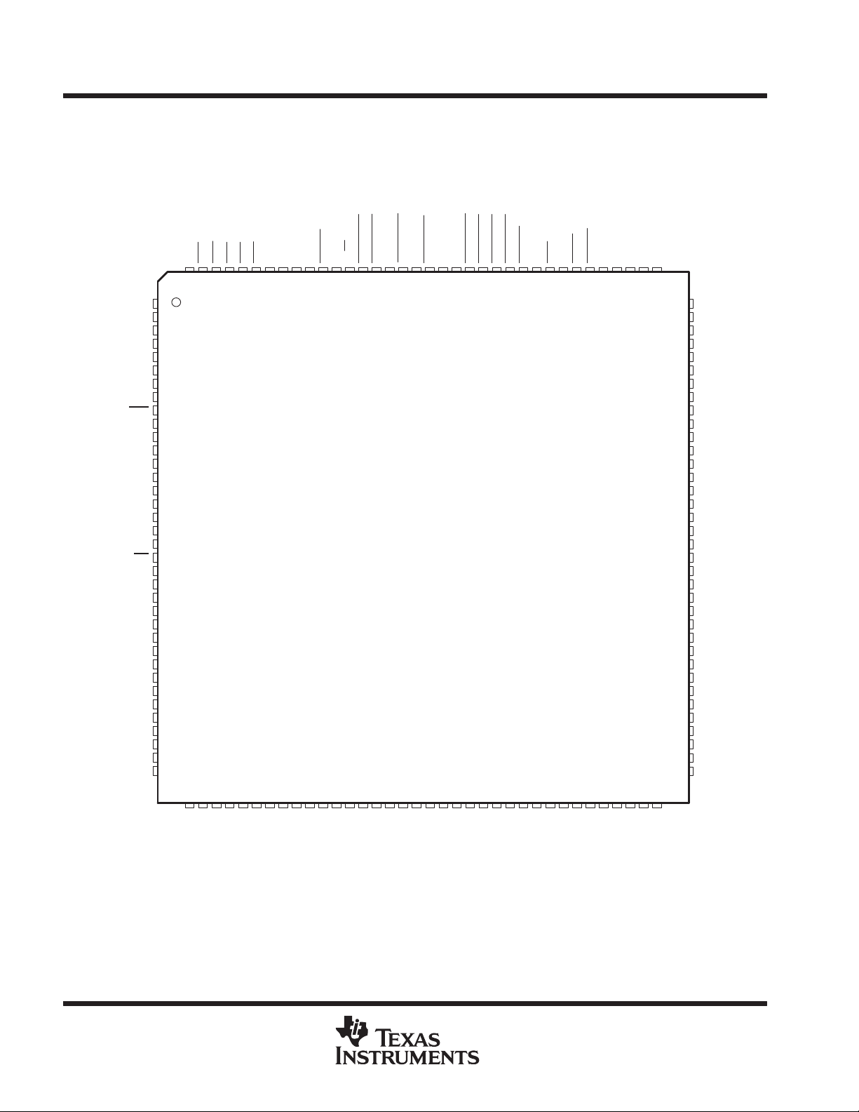
pin assignments
DR0
DV
DD
FSR0
CLKR0
CLKX0
FSX0
DX0
IV
SS
SHZ
TCLK0
TCLK1
DV
DD
EMU3
EMU0
V
DDL
V
DDL
EMU1
EMU2
V
SSL
MCBL/MP
CV
SS
DV
SS
A23
A22
A21
A20
A19
A18
DV
DD
A17
A16
A15
A14
A13
CV
SS
DV
SS
PCM PACKAGE
†
(TOP VIEW)
–2
–1
SS
SS
NC
INT3
INT2
INT1
INT0
IACK
XF1
XF0
144
143
142
141
140
139
138
1
2
3
4
5
6
7
8
9
10
11
12
13
14
15
16
17
18
19
20
21
22
23
24
25
26
27
28
29
30
31
32
33
34
35
36
373839404142434445464748495051525354555657585960616263646566676869
137DV136CV135
RESET
PRGW
134
133
R/W
STRB1_B0
132
131
DD
STRB1_B2/A
STRB1_B1
DV
130
129
128
SSL
V
127
STRB1_B3/A
126
DDL
V
125V124
DDL
STRB0_B0
STRB0_B1
123
122
–2
STRB0_B2/A
121
–1
STRB0_B3/A
120
SS
IOSTRB
119IV118
RDY
117DV116
DD
HOLD
HOLDA
115
114
SS
CLKIN
DV
113
112
SS
SUBS
CV
V
111
110
707172
NC
109
108
107
106
105
104
103
102
101
100
H3
H1
D0
D1
D2
D3
DV
DD
D4
D5
D6
99
D7
98
D8
97
D9
96
V
95
SSL
V
94
SSL
DV
93
SS
CV
92
SS
D10
91
DV
90
DD
D11
89
IV
88
SS
D12
87
V
86
DDL
V
85
DDL
D13
84
D14
83
D15
82
D16
81
D17
80
DV
79
DD
D18
78
D19
77
D20
76
D21
75
DV
74
SS
CV
73
SS
†
NC=No internal connection
2
NC
A12
DV
DD
A11
A9A8A7
A10
A6DDA5A4A3
DV
POST OFFICE BOX 1443 • HOUSTON, TEXAS 77251–1443
DDL
V
DDL
V
A2
SS
CV
SS
DV
A1
SSL
V
SSL
V
A0
DV
DD
D31
D30
D29
D28
D27
D26SSD25DDD24
IV
DV
D23
D22
NC
TMS320C32
DIGITAL SIGNAL PROCESSOR
SPRS027C – JANUARY 1995 – REVISED DECEMBER 1996
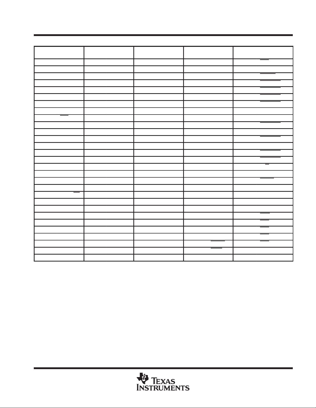
Pin Assignments
PIN PIN PIN PIN PIN
NUMBER NAME NUMBER NAME NUMBER NAME NUMBER NAME NUMBER NAME
1 DR0 30 A17 59 DV
2 DV
3 FSR0 32 A15 61 D30 90 DV
4 CLKR0 33 A14 62 D29 91 D10 120 STRB0_B3/A
5 CLKX0 34 A13 63 D28 92 CV
6 FSX0 35 CV
7 DX0 36 DV
8 IV
9 SHZ 38 A12 67 D25 96 D9 125 V
10 TCLK0 39 DV
11 TCLK1 40 A11 69 D24 98 D7 127 V
12 DV
13 EMU3 42 A9 71 D22 100 D5 129 DV
14 EMU0 43 A8 72 NC 101 D4 130 STRB1_B1
15 V
16 V
17 EMU1 46 DV
18 EMU2 47 A5 76 D20 105 D1 134 RESET
19 V
20 MCBL/MP 49 A3 78 D18 107 H1 136 DV
21 CV
22 DV
23 A23 52 A2 81 D16 110 V
24 A22 53 CV
25 A21 54 DV
26 A20 55 A1 84 D13 113 CLKIN 142 INT2
27 A19 56 V
28 A18 57 V
29 DV
DD
SS
DD
DDL
DDL
SSL
SS
SS
DD
31 A16 60 D31 89 D11 118 IV
SS
SS
37 NC 66 IV
DD
41 A10 70 D23 99 D6 128 STRB1_B2/A
44 A7 73 CV
45 A6 74 DV
DD
48 A4 77 D19 106 D0 135 CV
50 V
51 V
58 A0 87 D12 116 DV
DDL
DDL
SS
SS
SSL
SSL
64 D27 93 DV
65 D26 94 V
68 DV
75 D21 104 D2 133 PRGW
79 DV
80 D17 109 NC 138 XF1
82 D15 111 CV
83 D14 112 DV
85 V
86 V
DD
SS
DD
SS
SS
DD
DDL
DDL
88 IV
95 V
97 D8 126 STRB1_B3/A
102 DV
103 D3 132 R/W
108 H3 137 XF0
114 HOLDA 143 INT3
115 HOLD 144 NC
SS
DD
SS
SS
SSL
SSL
DD
SUBS
SS
SS
DD
117 RDY
SS
119 IOSTRB
121 STRB0_B2/A
122 STRB0_B1
123 STRB0_B0
124 V
131 STRB1_B0
139 IACK
140 INT0
141 INT1
DDL
DDL
SSL
DD
SS
SS
–1
–2
–1
–2
POST OFFICE BOX 1443 • HOUSTON, TEXAS 77251–1443
3
TMS320C32
TYPE
†
DESCRIPTION
DIGITAL SIGNAL PROCESSOR
SPRS027C – JANUARY 1995 – REVISED DECEMBER 1996
pin functions
This section provides signal descriptions for the TMS320C32 device. The following table lists each signal, the
number of pins, operating modes, and a brief signal description. The following table groups the signals
according to their function.
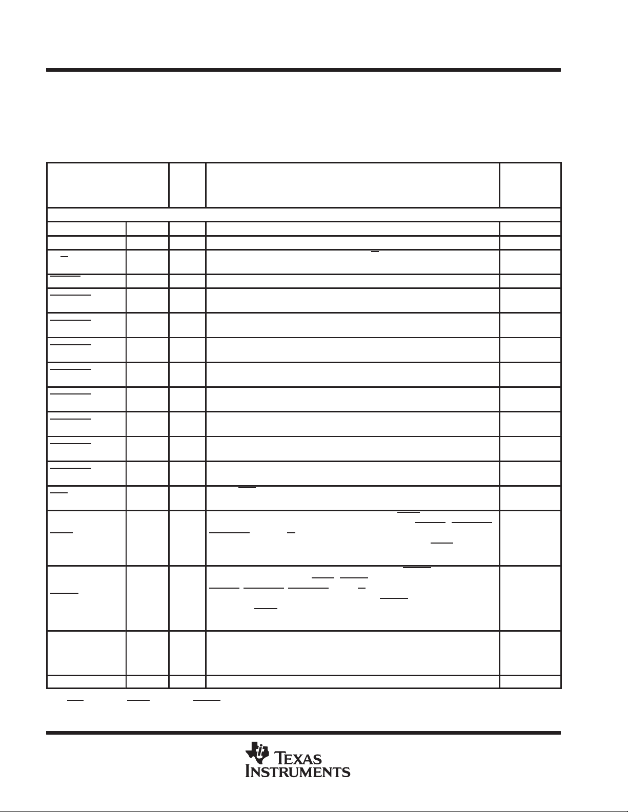
TMS320C32 Pin Functions
PIN
NAME NO.
EXTERNAL-BUS INTERFACE (70 PINS)
A23–A0 24 O/Z 24-bit address port of the external-bus interface S H R
D31–D0 32 I/O/Z 32-bit data port of the external-bus interface S H R
R/W 1 O/Z
IOSTRB 1 O/Z External-peripheral I/O strobe for the external-memory interface S H
STRB0_B3/A
STRB0_B2/A
STRB0_B1 1 O/Z
STRB0_B0 1 O/Z
STRB1_B3/A
STRB1_B2/A
STRB1_B1 1 O/Z
STRB1_B0 1 O/Z
RDY 1 I
HOLD 1 I
HOLDA 1 O/Z
PRGW 1 I
A23–A0 24 O/Z 24-bit address port of the external-bus interface S H R
†
I = input, O = output, Z = high-impedance state
‡
S = SHZ
–1
–2
–1
–2
active, H = HOLD active, R = RESET active
1 O/Z
1 O/Z
1 O/Z
1 O/Z
Read/write for external-memory interface. R/W is high when a read is performed
and low when a write is performed over the parallel interface.
External-memory access strobe 0, byte enable 3 for 32-bit external-memory
interface, and address pin for 8-bit and 16-bit external-memory interface
External-memory access strobe 0, byte enable 2 for 32-bit external-memory
interface, and address pin for 8-bit external-memory interface
External-memory access strobe 0, byte enable 1 for the external-memory
interface
External-memory access strobe 0, byte enable 0 for the external-memory
interface
External-memory access strobe 1, byte enable 3 for 32-bit external-memory
interface, and address pin for 8-bit and 16-bit external-memory interface
External-memory access strobe 1, byte enable 2 for 32-bit external-memory
interface, and address pin for 8-bit external-memory interface
External-memory access strobe 1, byte enable 1 for the external-memory
interface
External-memory access strobe 1, byte enable 0 for the external-memory
interface
Ready. RDY indicates that the external device is prepared for an externalmemory interface transaction to complete.
Hold signal for external-memory interface. When HOLD is a logic low, any
ongoing transaction is completed. A23 –A0, D31 –D0, IOSTRB
STRB1_Bx
transactions over the external-memory interface are held until HOLD
logic high or the NOHOLD bit of the STRB0 bus-control register is set.
Hold acknowledge for external-memory interface. HOLDA is generated in
response to a logic low on HOLD
IOSTRB
that all transactions over the memory are held. HOLDA
logic high of HOLD
is set.
Program memory width select. When PRGW is a logic low, program is fetched as
a single 32-bit word. When PRGW is a logic high, two 16-bit program fetches are
performed to fetch a single 32-bit instruction word. The status of PRGW at device
reset affects the reset value of the STRB0 and STRB1 bus-control register.
, and R/W are placed in the high-impedance state, and all
. HOLDA indicates that A23 – A0, D31 – D0,
, STRB0_Bx, STRB1_Bx, and R/W are in the high-impedance state and
is high in response to a
or when the NOHOLD bit of the external bus-control register
, STRB0_Bx,
becomes a
CONDITIONS
WHEN
SIGNAL IS
IN HIGH Z
S H
S H
S H
S H
S H
S H
S H
S H
S H
S
‡
4
POST OFFICE BOX 1443 • HOUSTON, TEXAS 77251–1443
TYPE
†
DESCRIPTION
TMS320C32
DIGITAL SIGNAL PROCESSOR
SPRS027C – JANUARY 1995 – REVISED DECEMBER 1996
TMS320C32 Pin Functions (Continued)
PIN
NAME NO.
CONTROL SIGNALS (9 PINS)
Reset. When RESET is a logic low, the device is in the reset condition. When
RESET
RESET 1 I
INT3–INT0 4 I External interrupts
IACK 1 O/Z
MCBL/MP 1 I Microcomputer boot loader/microprocessor mode
XF1–XF0 2 I/O/Z
CLKX0 1 I/O/Z
DX0 1 I/O/Z Data-transmit output. Serial port 0 transmits serial data on DX0. S R
FSX0 1 I/O/Z
CLKR0 1 I/O/Z
DR0 1 I/O/Z Data receive. Serial port 0 receives serial data on DR0. S R
FSR0 1 I/O/Z
TCLK0 1 I/O/Z
TCLK1 1 I/O/Z
CLKIN 1 I Input to the internal oscillator from an external clock source
H1 1 O/Z External H1 clock. H1 has a period equal to twice CLKIN. S
H3 1 O/Z External H3 clock. H3 has a period equal to twice CLKIN. S
EMU0–EMU2 3 I Reserved for emulation. Use 18 kΩ–22 kΩ pullup resistors to 5 V.
EMU3 1 O/Z Reserved for emulation S
SHZ 1 I
†
I = input, O = output, Z = high-impedance state
‡
S = SHZ
active, H = HOLD active, R = RESET active
becomes a logic high, execution begins from the location specified by the
reset vector.
Interrupt acknowledge. IACK is generated by the IACK instruction. This signal can
be used to indicate the beginning or end of an interrupt-service routine.
External flags. XF1 and XF0 are used as general-purpose I/Os or used to support
interlocked-processor instructions.
SERIAL PORT SIGNALS (6 PINS)
Serial-port 0 transmit clock. CLKX0 is the serial shift clock for the serial port 0
transmitter.
Frame-synchronization pulse for transmit. The FSX0 pulse initiates the
transmit-data process over DX0.
Serial-port 0 receive clock. CLKR0 is the serial-shift clock for the serial-port 0
receiver.
Frame-synchronization pulse for receive. The FSR0 pulse initiates the
receive-data process over DR0.
TIMER SIGNALS (2 PINS)
Timer clock 0. As an input, TCLK0 is used by timer 0 to count external pulses. As
an output, TCLK0 outputs pulses generated by timer 0.
Timer clock 1. As an input, TCLK1 is used by timer 1 to count external pulses. As
an output, TCLK1 outputs pulses generated by timer 1.
CLOCK SIGNALS (3 PINS)
RESERVED (5 PINS)
Shutdown high impedance. When active, SHZ shuts down the ’C32 and places
all 3-state I/O pins in the high-impedance state. SHZ
to ensure that no dual-drive conditions occur. CAUTION: A low on SHZ
’C32 memory and register contents. Reset the device with SHZ
to a known operating condition.
is used for board-level testing
corrupts
high to restore it
CONDITIONS
WHEN
SIGNAL IS
IN HIGH Z
S
S R
S R
S R
S R
S R
S R
S R
‡
POST OFFICE BOX 1443 • HOUSTON, TEXAS 77251–1443
5
TMS320C32
TYPE
†
DESCRIPTION
DIGITAL SIGNAL PROCESSOR
SPRS027C – JANUARY 1995 – REVISED DECEMBER 1996
TMS320C32 Pin Functions (Continued)
PIN
NAME NO.
CV
SS
DV
SS
IV
SS
DV
DD
V
DDL
V
SSL
V
SUBS
†
I = input, O = output, Z = high-impedance state
‡
S = SHZ
§
Recommended decoupling capacitor is 0.1 µF.
active, H = HOLD active, R = RESET active
7 I Ground
7 I Ground
4 I Ground
12 I + 5-V dc supply
8 I + 5-V dc supply
6 I Ground
1 I Substrate, tie to ground
POWER/GROUND
§
§
CONDITIONS
WHEN
SIGNAL IS
IN HIGH Z
‡
6
POST OFFICE BOX 1443 • HOUSTON, TEXAS 77251–1443
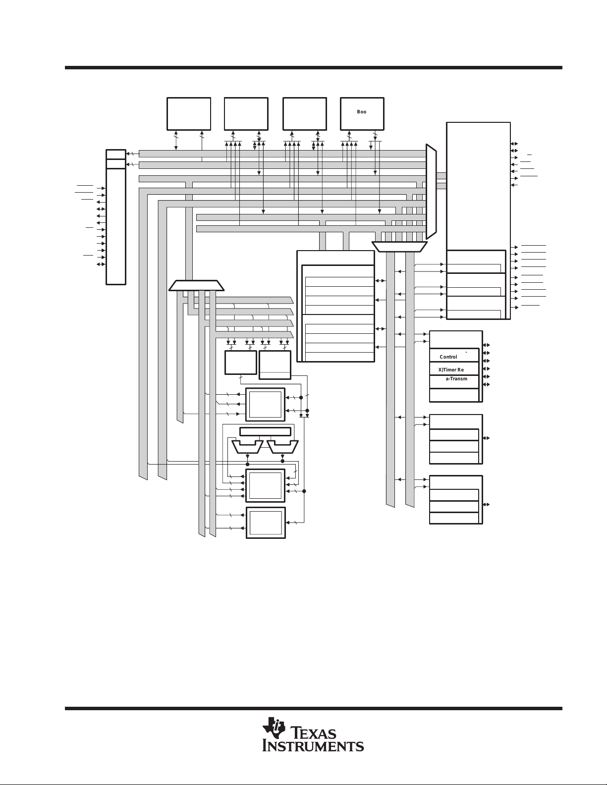
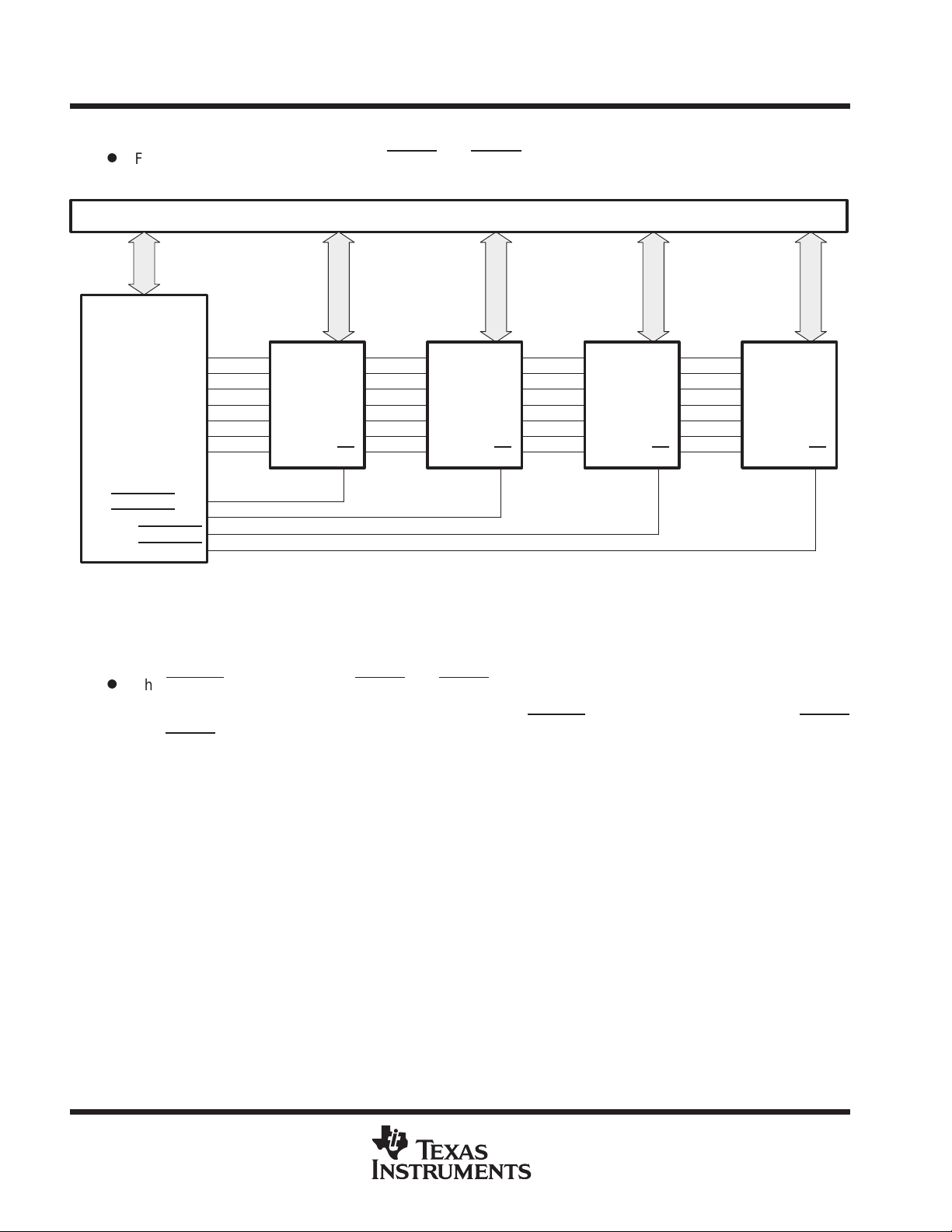
functional block diagram
TMS320C32
DIGITAL SIGNAL PROCESSOR
SPRS027C – JANUARY 1995 – REVISED DECEMBER 1996
RESET
INT(3-0)
IACK
XF(1,0)
MCBL / MP
CLKIN
V
V
SHZ
EMU0–3
Program
Cache
(64 × 32)
32 24
32
24
Controller
PDATA Bus
PADDR Bus
DDATA Bus
DADDR1 Bus
Multiplexer
CPU1
DADDR2 Bus
DMADATA Bus
DMAADDR Bus
REG1
IR
PC
H1
H3
DD
SS
RAM
Block 0
(256 × 32)
24
CPU1
CPU2
REG1
REG2
32 32 40 40
REG2
Multiplier
40
40
Extended-
40
Precision
Registers
32
(R0–R7)
DISP0, IR0, IR1
ARAU0 ARAU1
24
Auxiliary
24
Registers
32
(AR0 – AR7)
32
32
Other
32
Registers
RAM
Block 1
(256 × 32)
24 2432 32 32
DMA Controller
DMA Channel 0
Global-Contol Register
Source-AddressRegister
Destination-Address Reg.
Transfer-Counter Reg.
DMA Channel 1
Global-Control Register
Source-AddressRegister
Destination-Address Reg.
Transfer-Counter Reg.
40
40
40
24
24
32
32
BK
(12)
32-Bit
Barrel
Shifter
ALU
Boot
ROM
Multiplexer
Peripheral Data Bus
Peripheral Address Bus
Interface
Multiplexer
STRB0
STRB0 Control Reg.
STRB1
STRB1 Control Reg.
IOSTRB
IOSTRB Control Reg.
Serial Port
Serial Port-
Control Reg.
Receive/Transmit
(R/X)Timer Register
Data-Transmit
Register
Data-Receive
Register
Timer 0
Global-Control
Register
Timer-Period
Register
Timer-Counter
Register
Timer 1
Global-Control
Register
Timer-Period
Register
Timer-Counter
Register
External
Memory
FSX0
DX0
CLKX0
FSR0
DR0
CLKR0
TCLK0
TCLK1
A23 – A0
D31 – D0
R/W
RDY
HOLD
HOLDA
PRGW
STRB0_B3/A
STRB0_B2/A
STRB0_B1
STRB0_B0
STRB1_B3/A
STRB1_B2/A
STRB1_B1
STRB1_B0
IOSTRB
–1
–2
–1
–2
operation
Operation of the TMS320C32 is identical to the TMS320C30 and TMS320C31 digital signal processors, with
the exception of an enhanced external memory interface and the addition of two CPU power-management
modes.
external-memory interface
The TMS320C32 has a configurable external-memory interface with a 24-bit address bus, a 32-bit data bus,
and three independent multifunction strobes. The flexibility of this unique interface enables product designers
to minimize external-memory chip count.
POST OFFICE BOX 1443 • HOUSTON, TEXAS 77251–1443
7
TMS320C32
DIGITAL SIGNAL PROCESSOR
SPRS027C – JANUARY 1995 – REVISED DECEMBER 1996
external memory interface (continued)
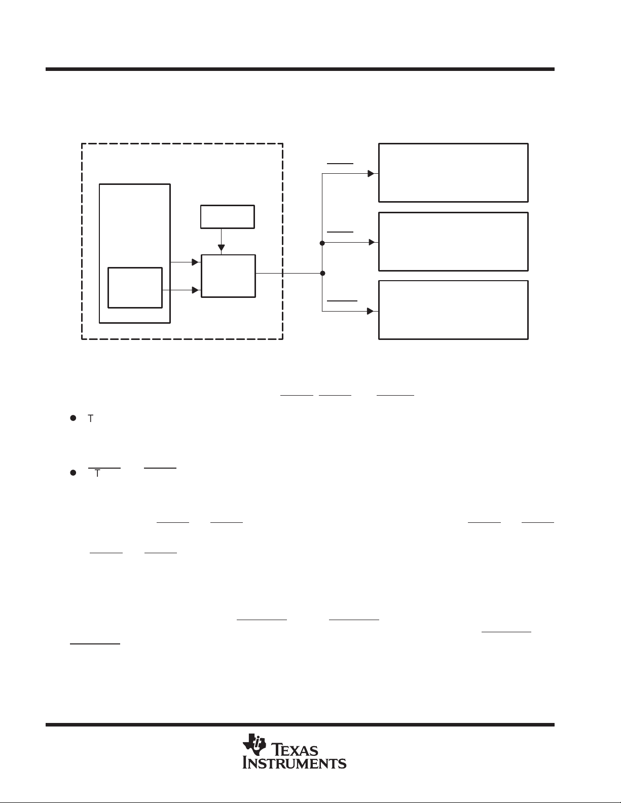
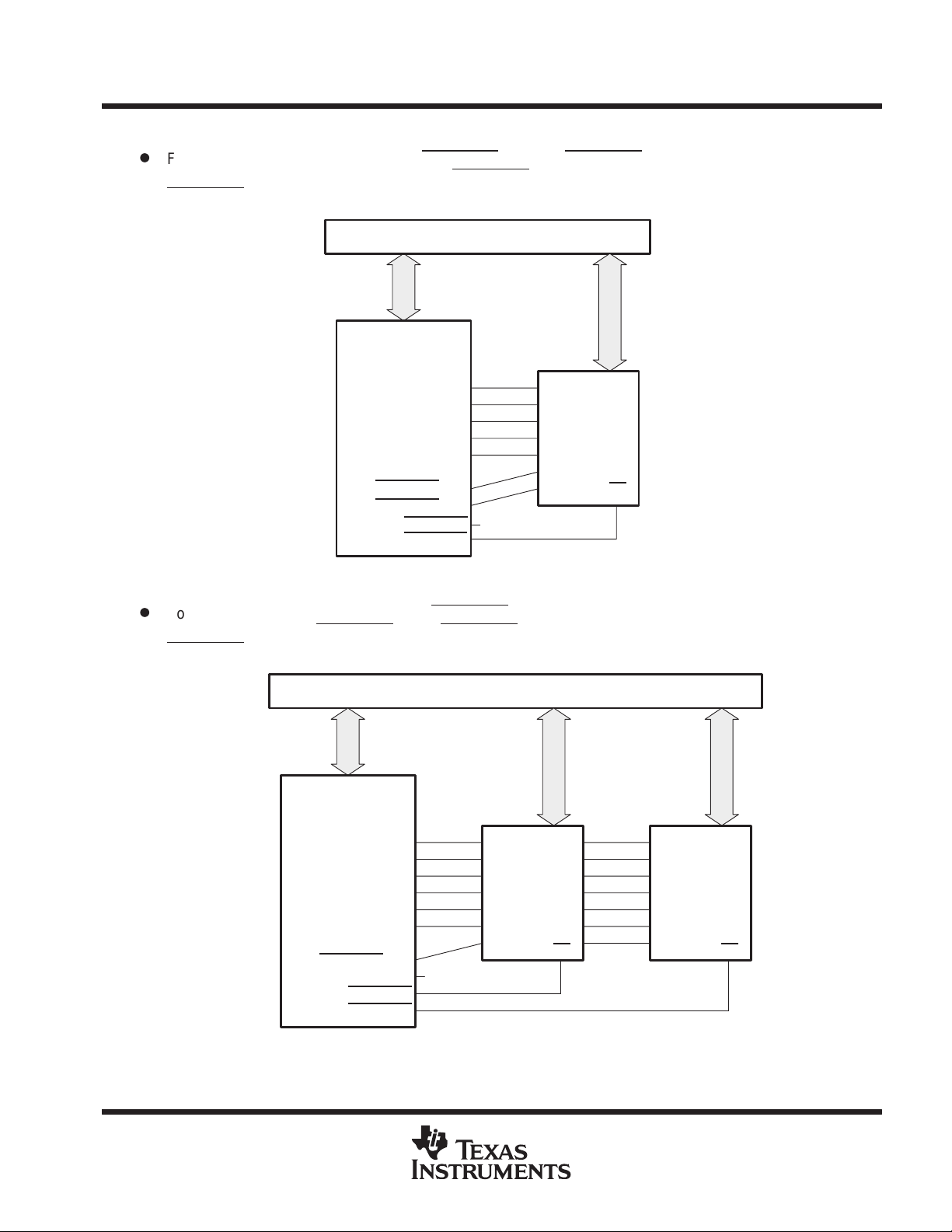
Up to three mutually exclusive memory areas (one program area and two data areas) can be implemented. Each
memory area configuration is independent of the physical memory width and independent of the configuration
of other memory areas. See Figure 1.
8-/16-/32-Bit Data in
8-/16-/32-Bit-Wide Memory
32-Bit Program in 16-/32-Bit-
Wide Memory
8-/16-/32-Bit Data in
8-/16-/32-Bit-Wide Memory
32-Bit Program in 16-/32-Bit-
Wide Memory
32-Bit Data in 32-Bit-Wide
Memory
32-Bit Program in 32-Bit-
Wide Memory
32-Bit
CPU
StrobeControl
Registers
’C32
PRGW Pin
Memory
Interface
STRB0
STRB1
IOSTRB
Figure 1. ’C32 External Memory Interface
The TMS320C32’s external-memory configuration is controlled by a combination of hardware configuration and
memory-mapped control registers and can be reconfigured dynamically. The signals that control
external-memory configuration are the PRGW, STRB0, STRB1, and IOSTRB. The signals work as follows:
D
The TMS320C32 is a 32-bit microprocessor, that is, the CPU operates on 32-bit program words. The
external-memory interface provides the capability of fetching instructions as either 32-bit words or two 16-bit
half words from consecutive addresses. Program memory width is 16 bits if the PRGW signal is high,
32 bits if the PRGW signal is low.
D
STRB0 and STRB1 are sets of control signals, four signals each, that are mapped to specific ranges of
external-memory addresses. When an address within one of these ranges is accessed by a read or write
instruction (CPU or DMA), the corresponding set of control signals is activated. Figure 8 illustrates the
TMS320C32 memory map, showing the address ranges for which the strobe signals become active.
The behavior of the STRB0
and STRB1 control signals is determined by the contents of the STRB0 and STRB1
control registers.
The STRB0
and STRB1 control registers each have a field that specifies the physical memory width (8, 16, or
32 bits) of the external-memory address ranges they control. Another field specifies the data width (8, 16, or
32 bits) of the data contained in those addresses. The values in these fields are not required to match. For
example, a 32-bit-wide physical memory space can be configured to segment each 32-bit word into four
consecutive 8-bit locations, each having its own address.
Each control-signal set has two pins (STRBx_B2
/A–2 and STRBx_B3/A–1) that can act as either byte-enable
(chip-select) pins or address pins, and two dedicated byte-enable (chip-select) pins (STRBx_B0 and
STRBx_B1). The pin functions are determined by the physical memory width specified in the corresponding
control register.
8
POST OFFICE BOX 1443 • HOUSTON, TEXAS 77251–1443
external memory interface (continued)
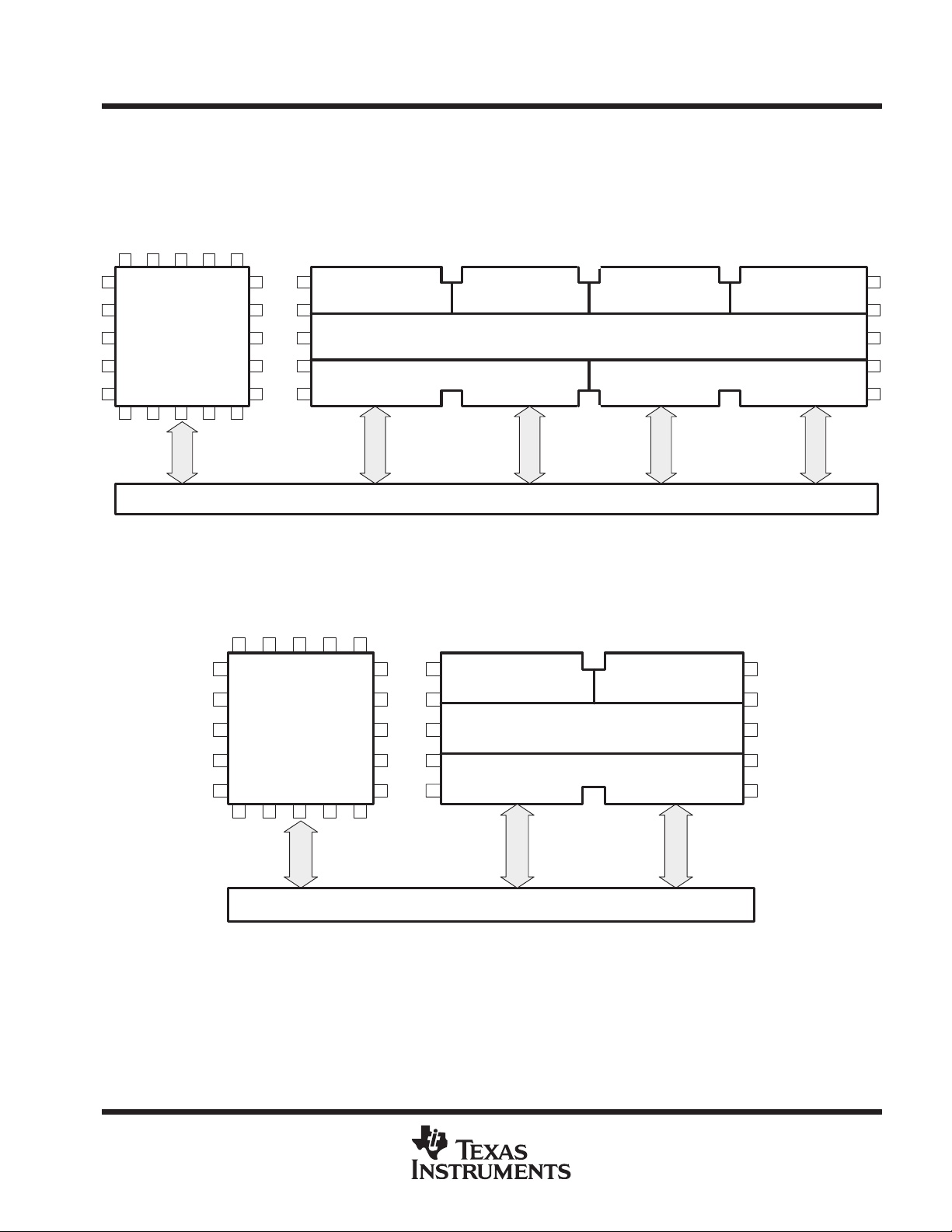
D
For 8-bit-wide physical memory, the STRBx_B2/A–2 and STRBx_B3/A–1 pins function as address pins
(least significant address bits) and the STRBx_B0 pin functions as a byte-enable (chip-select) pin.
STRBx_B1 is unused. See Figure 2.
TMS320C32
8
Data
STRB0_B3
STRB0_B2/A
/A
STRB0_B1
STRB0_B0
8-Bit Data Bus
A14
A13
A12
.
.
A1
A0
–1
–2
NC
TMS320C32
DIGITAL SIGNAL PROCESSOR
SPRS027C – JANUARY 1995 – REVISED DECEMBER 1996
8
A14
.
.
A3
A2
A1
A0
Data
Memory
CS
Figure 2. ’C32 With 8-Bit-Wide External Memory
D
For 16-bit-wide physical memory, the STRBx_B3/A–1 pin functions as an address pin (least significant
address bits). The STRBx_B0 and STRBx_B1 pins function as byte-enable (chip-select) pins.
STRBx_B2/A
is unused. See Figure 3.
–2
16
Data
A14
A13
TMS320C32
STRB0_B3/A
STRB0_B2/ A
STRB0_B1
STRB0_B0
A2
A1
A0
–1
–2
16-Bit Data Bus
8
A14
.
.
NC
.
A2
A1
A0
Data
Memory
CS
A14
.
..
A3A3
A2
A1
A0
8
Data
Memory
CS
Figure 3. ’C32 With 16-Bit-Wide External Memory
POST OFFICE BOX 1443 • HOUSTON, TEXAS 77251–1443
9
TMS320C32
DIGITAL SIGNAL PROCESSOR
SPRS027C – JANUARY 1995 – REVISED DECEMBER 1996
external memory interface (continued)
D
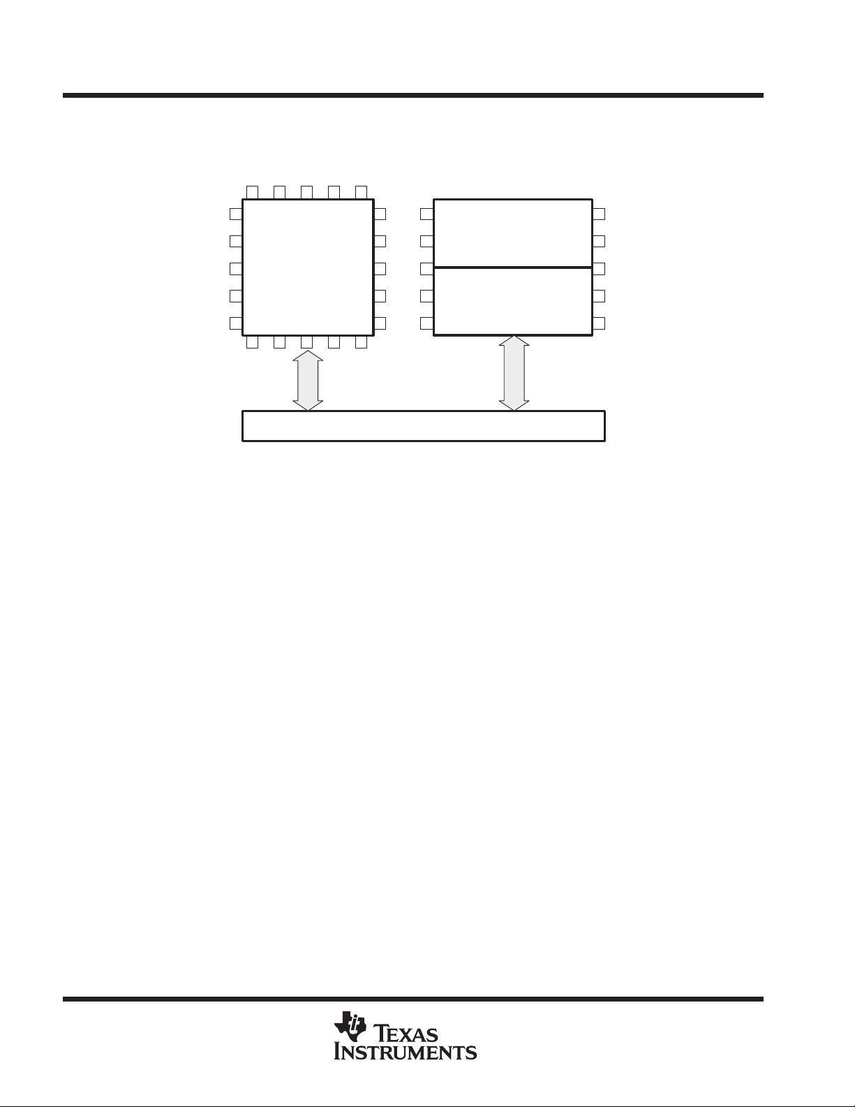
For 32-bit-wide physical memory, all STRB0 and STRB1 pins function as byte-enable (chip-select) pins.
See Figure 4.
32
32-Bit Data Bus
Data
A14
A13
.
.
A2
A1
A0
Data
CS
Memory
A14
A13
.
.
A2
A1
A0
TMS320C32
STRB0_B3/A
STRB0_B2/A
STRB0_B1
STRB0_B0
A14
A13
A2
A1
A0
–1
–2
Data
A14
A13
A2
A1
A0
.
.
Memory
CS
.
.
A14
A13
.
.
A2
A1
A0
Data
Memory
CS
Figure 4. ’C32 With 32-Bit-Wide External Memory
For more detailed information and examples see
(literature number SPRU132) and
Interfacing Memory to the TMS320C32 DSP Application Report
TMS320C32 Addendum to the TMS320C3x User’s Guide
number SPRA040).
D
The IOSTRB control signal, like STRB0 and STRB1, also is mapped to a specific range of addresses but
it is a single signal that can access only 32-bit data from 32-bit-wide memory . Its range of addresses appears
in the TMS320C32 memory map, shown in Figure 8. The IOSTRB
bus timing is different from the STRB0
and STRB1 bus timings to accommodate slower I/O peripherals.
8888
Data
Memory
CS
(literature
10
POST OFFICE BOX 1443 • HOUSTON, TEXAS 77251–1443
TMS320C32
DIGITAL SIGNAL PROCESSOR
SPRS027C – JANUARY 1995 – REVISED DECEMBER 1996
external memory interface (continued)
examples
Figure 5 and Figure 6 show examples of external memory configurations that can be implemented using the
TMS320C32 external memory interface. The first example has a 32-bit-wide external memory with 8- and 16-bit
data areas and a 32-bit program area.
32-Bit-Wide Memory
8-Bit Data 8-Bit Data8-Bit Data
32-Bit Program
16-Bit Data16-Bit Data
8 8 8
320C32
32
8-Bit Data
8
32-Bit-Wide Data Bus
Figure 5. 32-Bit-Wide External Memory Configured With 8- and 16-Bit Data Areas and 32-Bit Program
Memory
Figure 6 shows a configuration that can be implemented with 16-bit external memory. The 32-bit data and
program words can be stored and retrieved as half-words.
16-Bit-Wide Memory
8-Bit Data
320C32
8-Bit Data
32-Bit Program
16-Bit Data
16
16-Bit-Wide Data Bus
88
Figure 6. 16-Bit-Wide External Memory Configured With 8- and 16-Bit Data Areas and a 32-Bit Program
Area
POST OFFICE BOX 1443 • HOUSTON, TEXAS 77251–1443
11
TMS320C32
DIGITAL SIGNAL PROCESSOR
SPRS027C – JANUARY 1995 – REVISED DECEMBER 1996
external memory interface (continued)
Figure 7 shows one possible configuration that can be implemented with 8-bit external memory. Program words,
which are 32-bit, cannot be executed from 8-bit-wide memory.
8-Bit-Wide Memory
8-Bit Data
320C32
16-Bit Data
8
8-Bit-Wide Data Bus
8
Figure 7. 8-Bit-Wide External Memory Configured With 8- and 16-Bit Data Areas
12
POST OFFICE BOX 1443 • HOUSTON, TEXAS 77251–1443
ИИИИИИИИИИ
ИИИИИИИИИИ
ИИИИИИИИИИ
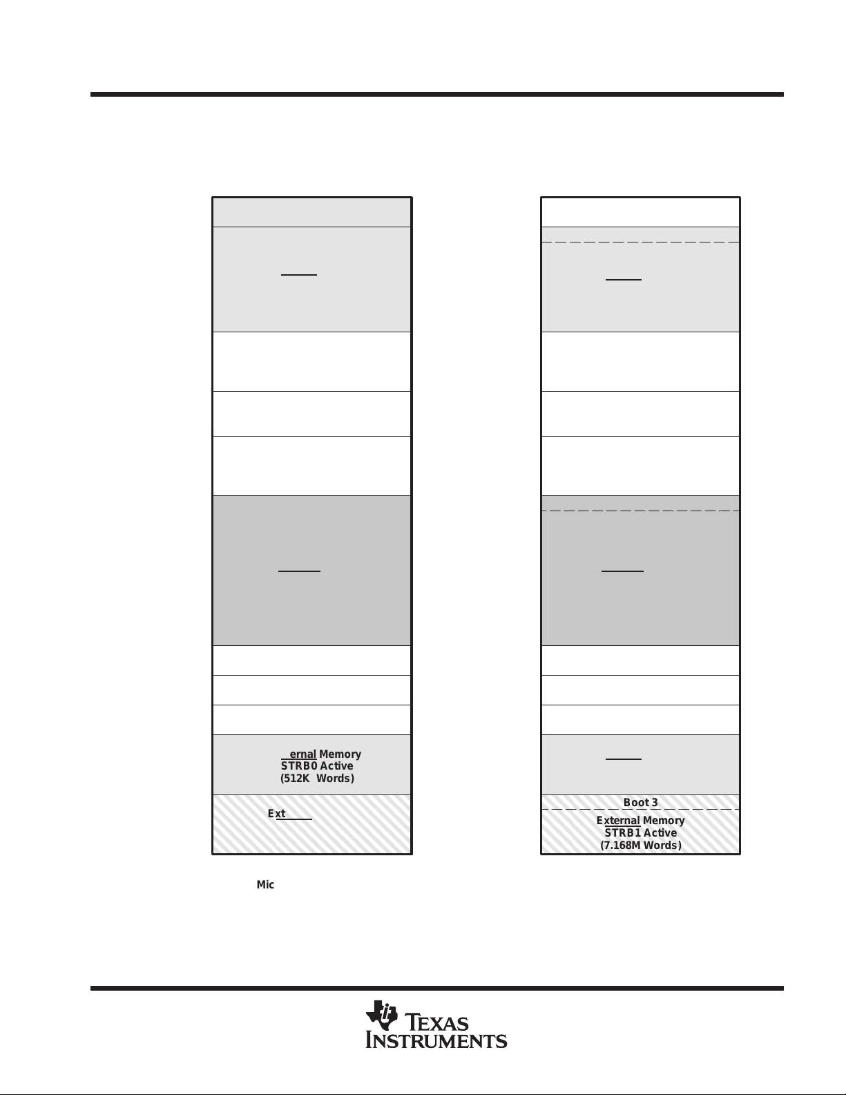
memory map
TMS320C32
DIGITAL SIGNAL PROCESSOR
SPRS027C – JANUARY 1995 – REVISED DECEMBER 1996
Figure 8 depicts the memory map for the TMS320C32. Refer to theTMS320C32 Addendum to the
User’s Guide
(literature number SPRU132) for a detailed description of this memory mapping, with shading to
indicate external memory.
0h
7FFFFFh
800000h
807FFFh
808000h
8097FFh
809800h
80FFFFh
810000h
Reset-Vector Location
External Memory
Memory-Mapped Registers
(6K-Word Internal)
Active
STRB0
(8.192M Words)
Reserved
(32K Words)
Peripheral-Bus
Reserved
(26K Words)
0h
FFFh
1000h
1001h
7FFFFFh
800000h
807FFFh
808000h
8097FFh
809800h
80FFFFh
810000h
810001h
Reserved for
Boot-Loader Operations
Boot 1
External Memory
STRB0
Active
(8.188M Words)
Reserved
(32K Words)
Peripheral-Bus
Memory-Mapped Registers
(6K-Word Internal)
Reserved
(26K Words)
Boot 2
TMS320C3x
82FFFFh
830000h
87FDFFh
87FE00h
87FEFFh
87FF00h
87FFFFh
880000h
8FFFFFh
900000h
FFFFFFh
External Memory
(314.5K Words)
(256-Word Internal)
(256-Word Internal)
External Memory
External Memory
STRB1
(7.168M Words)
Microprocessor Mode Microcomputer/Boot-LoaderMode
Active
IOSTRB
(128K Words)
Reserved
RAM Block 0
RAM Block 1
STRB0 Active
(512K Words)
Active
82FFFFh
830000h
87FDFFh
87FE00h
87FEFFh
87FF00h
87FFFFh
880000h
8FFFFFh
900000h
900001h
FFFFFFh
RAM Block 0 (256-Word Internal)
RAM Block 1 (256-Word Internal)
External Memory
IOSTRB
(319.5K Words)
External Memory
External Memory
(7.168M Words)
Active
(128K Words)
Reserved
Active
STRB0
(512K Words)
Boot 3
STRB1
Active
Figure 8. TMS320C32 Memory Map
POST OFFICE BOX 1443 • HOUSTON, TEXAS 77251–1443
13

TMS320C32
DIGITAL SIGNAL PROCESSOR
SPRS027C – JANUARY 1995 – REVISED DECEMBER 1996
power management
The TMS320C32 CPU has two power-management modes, IDLE2 and LOPOWER (low power). In IDLE2
mode, no instructions are executed and the CPU, peripherals, and memory retain their previous state while the
external bus output pins are idle. During IDLE2 mode, the H1 clock signal is held high while the H3 clock signal
is held low until one of the four external interrupts is asserted. In the LOPOWER mode, the CPU continues to
execute instructions and the DMA continues to perform transfers, but at a reduced clock rate of the CLKIN
frequency divided by 16 (that is, TMS320C32 with a 32-MHz CLKIN frequency performs the same as a 2-MHz
TMS320C32 with an instruction cycle time of 1000 ns (1 MHz).
boot loader
The TMS320C32 flexible boot loader loads programs from the serial port, EPROM, or other standard
non-volatile memory device. The boot-loader functionality of the TMS320C32 is equivalent to that of the
TMS320C31, and has added modes to handle the data-type sizes and memory widths supported by the external
memory interface. The memory-boot load supports data transfers with and without handshaking. The
handshake mode allows synchronous transfer of programs by using two pins as data-acknowledge and
data-ready signals.
peripherals
The TMS320C32 peripherals are composed of one serial port, two timers, and two DMA channels. The serial
port and timers are the functional equivalent of those in the TMS320C31 peripherals. The TMS320C32
two-channel DMA coprocessor has user-configurable priorities: CPU, DMA, or rotating between CPU and DMA.
14
POST OFFICE BOX 1443 • HOUSTON, TEXAS 77251–1443

TMS320C32
DIGITAL SIGNAL PROCESSOR
SPRS027C – JANUARY 1995 – REVISED DECEMBER 1996
peripherals (continued)
Figure 9 shows the TMS320C32’s peripheral-bus control-register mapping, with the reserved areas shaded.
808000h
808004h
808006h
808008h
808009h
808010h
808014h
808016h
808018h
808020h
808024h
808028h
808030h
808034h
808038h
DMA 0 Global Control
DMA 0 Source Address
DMA 0 Destination Address
DMA 0 Transfer Counter
DMA 1 Global Control
DMA 1 Source Address
DMA 1 Destination Address
DMA 1 Transfer Counter
Timer 0 Global Control
Timer 0 Counter
Timer 0 Period
Timer 1 Global Control
Timer 1 Counter
Timer 1 Period Register
808040h
808042h
808043h
808044h
808045h
808046h
808048h
80804Ch
808050h
Serial Port Global Control
FSX/DX/CLKX Port Control
FSR/DR/CLKR Port Control
R/X Timer Control
R/X Timer Counter
R/X Timer Period
Data Transmit
Data Receive
Reserved
80805Fh
808060h
808064h
808068h
IOSTRB-BusControl
STRB0-BusControl
STRB1-BusControl
808069h
Reserved
8097FFh
Figure 9. Peripheral-Bus Memory-Mapped Registers
Reserved
POST OFFICE BOX 1443 • HOUSTON, TEXAS 77251–1443
15

TMS320C32
DIGITAL SIGNAL PROCESSOR
SPRS027C – JANUARY 1995 – REVISED DECEMBER 1996
interrupts
T o reduce external logic and simplify the interface, the external interrupts can be either edge- or level-triggered.
Unlike the fixed interrupt-trap vector-table location of the TMS320C30 and TMS320C31 devices, the
TMS320C32 has a user-relocatable interrupt-trap vector table. The interrupt-trap vector table must start on a
256-word boundary . Figure 10 shows the interrupt and trap vector locations memory mapping with shading to
indicate reserved areas. The reset vector is fixed to address 0h as shown in Figure 8.
EA (ITTP) + 00h
EA (ITTP) + 01h
EA (ITTP) + 02h
EA (ITTP) + 03h
EA (ITTP) + 04h
EA (ITTP) + 05h
EA (ITTP) + 06h
EA (ITTP) + 07h
EA (ITTP) + 08h
EA (ITTP) + 09h
EA (ITTP) + 0Ah
EA (ITTP) + 0Dh
EA (ITTP) + 1Fh
Reserved
INT0
INT1
INT2
INT3
XINT0
RINT0
Reserved
Reserved
TINT0
TINT1
DINT0EA (ITTP) + 0Bh
DINT1EA (ITTP) + 0Ch
Reserved
16
EA (ITTP) + 20h TRAP0
.
.
.
.
EA (ITTP) + 3Bh
EA (ITTP) + 3Ch
EA (ITTP) + 3Dh
EA (ITTP) + 3Eh
EA (ITTP) + 3Fh
TRAP27
TRAP28
TRAP29
TRAP30
TRAP31
Reserved
Figure 10. Reset, Interrupt, and Trap Vector/Branches Memory-Map Locations
POST OFFICE BOX 1443 • HOUSTON, TEXAS 77251–1443

VIHHigh-level input voltage
T
C
TMS320C32
DIGITAL SIGNAL PROCESSOR
SPRS027C – JANUARY 1995 – REVISED DECEMBER 1996
absolute maximum ratings over specified temperature ranges (unless otherwise noted)
Supply voltage range, V
(see Note 1) –0.3 V to 7 V . . . . . . . . . . . . . . . . . . . . . . . . . . . . . . . . . . . . . . . . . . . . . .
CC
†
Input voltage range – 0.3 V to 7 V. . . . . . . . . . . . . . . . . . . . . . . . . . . . . . . . . . . . . . . . . . . . . . . . . . . . . . . . . . . . . . . .
Output voltage range, VO – 0.3 V to 7 V. . . . . . . . . . . . . . . . . . . . . . . . . . . . . . . . . . . . . . . . . . . . . . . . . . . . . . . . . . .
Continuous power dissipation (see Note 2) 1.95 W. . . . . . . . . . . . . . . . . . . . . . . . . . . . . . . . . . . . . . . . . . . . . . . . . .
Operating case temperature, T
(PCM (commercial) 0°C to 85°C. . . . . . . . . . . . . . . . . . . . . . . . . . . . . . . . . .
C
(PCMA (extended) – 40°C to 125°C. . . . . . . . . . . . . . . . . . . . . . . . . . . . . . .
Storage temperature range, T
†
Stresses beyond those listed under “absolute maximum ratings” may cause permanent damage to the device. These are stress ratings only, and
functional operation of the device at these or any other conditions beyond those indicated under “recommended operating conditions” is not
implied. Exposure to absolute-maximum-rated conditions for extended periods may affect device reliability.
NOTES: 1. All voltage values are with respect to VSS.
2. This value calculated for the ’C32-40. Actual operating power is less. This value was obtained under specially produced worst-case
test conditions which are not sustained during normal device operation. These conditions consist of continuous parallel writes of
a checkerboard pattern to the external bus at the maximum rate possible. See normal (IDD) current specification in the electrical
characteristics table and refer the
recommended operating conditions (see Note 3)
V
Supply voltage (DVDD, V
DD
V
Supply voltage (CVSS, V
SS
p
V
Low-level input voltage – 0.3
IL
I
High-level output current – 300 µA
OH
I
Low-level output current 2 mA
OL
Operating case temperature (commercial) 0 85 °C
Operating case temperature (extended) – 40 125 °C
‡
All nominal values are at VDD = 5 V, TA (ambient air temperature)= 25°C.
§
These values are derived from characterization and not tested.
NOTE 3: All input and output voltage levels are TTL compatible.
DDL
SSL
– 55°C to 150°C. . . . . . . . . . . . . . . . . . . . . . . . . . . . . . . . . . . . . . . . . . . . . . . . . .
stg
Calculation of TMS320C30 Power Dissipation Application Report
(literature number SPRU031)
‡
MIN NOM
) 4.75 5 5.25 V
, IVSS, DVSS, V
) 0 V
SUBS
CLKIN 2.6 VDD+ 0.3
All other inputs 2 VDD+ 0.3
§
‡
MAX UNIT
0.8 V
§
§
.
V
V
POST OFFICE BOX 1443 • HOUSTON, TEXAS 77251–1443
17
TMS320C32
T
A
25 C
Supply current
(
)
(see Note 4)
DIGITAL SIGNAL PROCESSOR
SPRS027C – JANUARY 1995 – REVISED DECEMBER 1996
electrical characteristics over recommended ranges of supply voltage (unless otherwise noted)
PARAMETER TEST CONDITIONS MIN NOM MAX UNIT
V
OH
V
OL
I
OZ
I
I
I
DD
C
I
C
o
†
All nominal values are at VDD = 5 V, TA (ambient air temperature) = 25°C.
‡
fx is the input clock frequency.
§
VOL(max) = 0.7 V for A(0:23)
¶
Assured by design but not tested
NOTE 4: Actual operating current is less than this maximum value (reference Note 2).
High-level output voltage VDD = MIN, IOH = MAX 2.4 3 V
15
§
mA
¶
pF
¶
pF
Low-level output voltage VDD = MIN, IOL = MAX 0.3 0.6
High-impedance state output current VDD = MAX – 20 20 µA
Input current VI = VSS to V
fx = 40 MHz
pp
see Note 4
Input capacitance
Output capacitance 20
fx = 50 MHz
fx = 60 MHz
Standby
All other
inputs
=
=
VDD = MAX,
fx = MAX
IDLE2,
CLKIN shut off
DD
°
,
‡
– 10 10 µA
160 390
200 425
225 475
50 µA
V
PARAMETER MEASUREMENT INFORMATION
†‡
Tester Pin
Electronics
Where: I
I
V
C
OL
OH
I
OL
V
Load
I
= 2 mA (all outputs)
= 300 µA (all outputs)
= 2.15 V
Load
= 80-pF typical load-circuit capacitance
T
Figure 11. Test Load Circuit
OH
Output
Under
C
T
Test
18
POST OFFICE BOX 1443 • HOUSTON, TEXAS 77251–1443

TMS320C32
DIGITAL SIGNAL PROCESSOR
SPRS027C – JANUARY 1995 – REVISED DECEMBER 1996
PARAMETER MEASUREMENT INFORMATION (CONTINUED)
signal-transition levels for ’C32 (see Figure 12 and Figure 13)
TTL-level outputs are driven to a minimum logic-high level of 2.4 V and to a maximum logic-low level of 0.6 V .
Output transition times are specified in the following paragraph.
For a high-to-low transition on an output signal, the level at which the output is said to be no longer high is
2 V and the level at which the output is said to be low is 1 V . For a low-to-high transition, the level at which the
output is said to be no longer low is 1 V and the level at which the output is said to be high is 2 V (see Figure 12).
2.4 V
2 V
1 V
0.6 V
Figure 12. ’C32 Output Levels
Transition times for TTL-compatible inputs are specified as follows. For a high-to-low transition on an input
signal, the level at which the input is said to be no longer high is 2 V and the level at which the input is said to
be low is 0.8 V . For a low-to-high transition on an input signal, the level at which the input is said to be no longer
low is 0.8 V and the level at which the input is said to be high is 2 V (see Figure 13).
2 V
Figure 13. ’C32 Input Levels
0.8 V
POST OFFICE BOX 1443 • HOUSTON, TEXAS 77251–1443
19
TMS320C32
DIGITAL SIGNAL PROCESSOR
SPRS027C – JANUARY 1995 – REVISED DECEMBER 1996
PARAMETER MEASUREMENT INFORMATION (CONTINUED)
timing parameter symbology
Timing parameter symbols used in this document are in accordance with JEDEC Standard 100-A. Unless
otherwise noted, in order to shorten the symbols, pin names and other related terminology have been
abbreviated as follows:
A23–A0 when the physical-memory-width-bit field of the STRBx control register is set to 32 bits
A23–A0 and STRBx_B3/A–1 when the physical-memory-width-bit field of the STRBx control register is
A
CI CLKIN
RDY RDY
D D(31–0)
H H1, H3
IOS IOSTRB
Pt
Qt
RW R/W
S
XF XF0 or XF1
set to 16 bits
A23–A0, STRBx_B3/A
control register is set to 8 bits
c(H)
c(CI)
STRBx_B(3–0) when the physical-memory-width-bit field of the STRBx control register is set to 32 bits
STRBx_B(1–0) when the physical-memory-width-bit field of the STRBx control register is set to 16 bits
STRBx_B0
when the physical-memory-width-bit field of the STRBx control register is set to 8 bits
and STRBx_B2/A–2 when the physical-memory-width-bit field of the STRBx
–1,
20
POST OFFICE BOX 1443 • HOUSTON, TEXAS 77251–1443

NO
PARAMETERS
UNIT
TMS320C32
DIGITAL SIGNAL PROCESSOR
SPRS027C – JANUARY 1995 – REVISED DECEMBER 1996
operating characteristics for CLKIN, H1 and H3 [Q = t
.
1 t
f(CI)
2 t
w(CIL)
3 t
w(CIH)
4 t
r(CI)
5 t
c(CI)
6 t
f(H)
7 t
w(HL)
8 t
w(HH)
9 t
r(H)
9.1 t
d(HL-HH)
10 t
†
‡
c(H)
The minimum CLKIN high pulse duration at 3.3 MHz is 10 ns.
Assured by design but not tested
Fall time, CLKIN 5
Pulse duration, CLKIN low Q = MIN 9 7 6 ns
Pulse duration, CLKIN high Q = MIN 9
Rise time, CLKIN 5
Cycle time, CLKIN 25 303 20 303 16.67 303 ns
Fall time, H1/H3 3 3 3 ns
Pulse duration, H1/H3 low Q–5 Q–5 Q–4 ns
Pulse duration, H1/H3 high Q–6 Q–6 Q–5 ns
Rise time, H1/H3 3 3 3 ns
Delay time, H1/H3 low to H1/H3 high 0 4 0 4 0 4 ns
Cycle time, H1/H3 50 606 40 606 33.33 606 ns
1
CLKIN
4
TEST
CONDITIONS
5
] (see Figure 14 and Figure 15)
c(CI)
’C32-40 ’C32-50 ’C32-60
MIN MAX MIN MAX MIN MAX
‡
†
†
8
‡
‡
5
‡
5
‡
4
ns
†
6
ns
‡
4
ns
H1
H3
3
2
Figure 14. CLKIN Timing
10
9
8
9.1
7
10
6
7
9.1
8
9
Figure 15. H1/H3 Timing
6
POST OFFICE BOX 1443 • HOUSTON, TEXAS 77251–1443
21

TMS320C32
NO
UNIT
DIGITAL SIGNAL PROCESSOR
SPRS027C – JANUARY 1995 – REVISED DECEMBER 1996
memory-read-cycle and memory-write-cycle timing (STRBx) (see Figure 16 and Figure 17)
.
11 t
d(H1L-SL)
12 t
d(H1L-SH)
13 t
d(H1H-RWL)
14 t
d(H1L-A)
15 t
su(D)R
16 t
h(D)R
17 t
su(RDY)
18 t
h(RDY)
19 t
d(H1H-RWH)
20 t
v(D)W
21 t
h(D)W
22 t
d(H1H-A)
†
Assured from characterization but not tested
Delay time, H1 low to STRBx low 0
Delay time, H1 low to STRBx high 0
Delay time, H1 high to R/W low (read) 0
Delay time, H1 low to A valid 0
Setup time, D valid before H1 low (read) 13 10 10 ns
Hold time, D after H1 low (read) 0 0 0 ns
Setup time, RDY before H1 low 21 19 17 ns
Hold time, RDY after H1 low 0 0 0 ns
Delay time, H1 high to R/W high (write) 11 9 8 ns
Valid time, D after H1 low (write) 17 14 12 ns
Hold time, D after H1 high (write) 0 0 0 ns
Delay time, H1 high to A valid on back-to-back write
cycles
’C32-40 ’C32-50 ’C32-60
MIN MAX MIN MAX MIN MAX
†
11 0
†
11 0
†
11 0
†
11 0
11 9 8 ns
†
9 0
†
9 0
†
9 0
†
9 0
†
†
†
†
7 ns
7 ns
8 ns
7 ns
H3
H1
‡
STRBx
R/W
A
D
RDY
‡
STRBx remains low during back-to-back operations.
Figure 16. Memory-Read-Cycle Timing
11
14
12
15
13
16
18
17
22
POST OFFICE BOX 1443 • HOUSTON, TEXAS 77251–1443

TMS320C32
DIGITAL SIGNAL PROCESSOR
SPRS027C – JANUARY 1995 – REVISED DECEMBER 1996
memory-read-cycle and memory-write-cycle timing (STRBx) (see Figure 16 and Figure 17)
(continued)
H3
H1
STRBx
R/W
RDY
11
13
14
A
20
D
12
19
22
21
18
17
Figure 17. Memory-Write-Cycle Timing
POST OFFICE BOX 1443 • HOUSTON, TEXAS 77251–1443
23

TMS320C32
NO
UNIT
DIGITAL SIGNAL PROCESSOR
SPRS027C – JANUARY 1995 – REVISED DECEMBER 1996
memory-read-cycle timing using IOSTRB (see Figure 18)
.
11.1 t
d(H3L-IOSL)
12.1 t
d(H3L-IOSH)
13.1 t
d(H1L-RWL)
14.1 t
d(H1L-A)
15.1 t
su(D)R
16.1 t
h(D)R
17.1 t
su(RDY)
18.1 t
h(RDY)
23 t
†
d(H1L-RWH)
Assured from characterization but not tested
Delay time, H3 low to IOSTRB low 0
Delay time, H3 low to IOSTRB high 0
Delay time, H1 low to R/W high 0
Delay time, H1 low to A valid 0
Setup time, D before H1 high 13 10 9 ns
Hold time, D after H1 high 0 0 0 ns
Setup time, RDY before H1 high 9 8 7 ns
Hold time, RDY after H1 high 0 0 0 ns
Delay time, H1 low to R/W low 0
H3
’C32-40 ’C32-50 ’C32-60
MIN MAX MIN MAX MIN MAX
†
11 0
†
11 0
†
11 0
†
11 0
†
11 0
†
9 0
†
9 0
†
9 0
†
9 0
†
9 0
†
†
†
†
†
8 ns
8 ns
8 ns
8 ns
8 ns
H1
11.1 12.1
IOSTRB
13.1
R/W
14.1
A
15.1
D
17.1
RDY
†
See Figure 19 and accompanying table.
16.1
18.1
Figure 18. Memory-Read-Cycle Timing Using IOSTRB
23
†
24
POST OFFICE BOX 1443 • HOUSTON, TEXAS 77251–1443

NO
UNIT
memory-write-cycle timing using IOSTRB (see Figure 19)
.
11.1 t
d(H3L-IOSL)
12.1 t
d(H3L-IOSH)
13.1 t
d(H1L-RWL)
14.1 t
d(H1L-A)
17.1 t
su(RDY)
18.1 t
h(RDY)
23 t
d(H1L-RWH)
24 t
v(D)W
25 t
†
h(D)W
Assured from characterization but not tested
Delay time, H3 low to IOSTRB low 0
Delay time, H3 low to IOSTRB high 0
Delay time, H1 low to R/W high 0
Delay time, H1 low to A valid 0
Setup time, RDY before H1 high 9 8 7 ns
Hold time, RDY after H1 high 0 0 0 ns
Delay time, H1 low to R/W low 0
Valid time, D after H1 high 17 14 12 ns
Hold time, D after H1 low 0 0 0 ns
H3
TMS320C32
DIGITAL SIGNAL PROCESSOR
SPRS027C – JANUARY 1995 – REVISED DECEMBER 1996
’C32-40 ’C32-50 ’C32-60
MIN MAX MIN MAX MIN MAX
†
11 0
†
11 0
†
11 0
†
11 0
†
11 0
†
†
†
†
†
9 0
9 0
9 0
9 0
9 0
†
8 ns
†
8 ns
†
8 ns
†
8 ns
†
8 ns
H1
†
11.1
IOSTRB
†
23
R/W
†
14.1
A
D
RDY
†
See Figure 18 and accompanying table.
17.1
†
12.1
24 25
†
18.1
Figure 19. Memory-Write-Cycle Timing Using IOSTRB
†
13.1
†
POST OFFICE BOX 1443 • HOUSTON, TEXAS 77251–1443
25

TMS320C32
NO
UNIT
DIGITAL SIGNAL PROCESSOR
SPRS027C – JANUARY 1995 – REVISED DECEMBER 1996
timing for XF0 and XF1 when executing LDFI or LDII (see Figure 20)
.
38 t
39 t
40 t
d(H3H-XF0L)
su(XF1)
h(XF1)
Delay time, H3 high to XF0 low 13 12 11 ns
Setup time, XF1 before H1 low 9 9 8 ns
Hold time, XF1 after H1 low 0 0 0 ns
’C32-40 ’C32-50 ’C32-60
MIN MAX MIN MAX MIN MAX
H3
H1
STRBx
R/W
A
D
RDY
XF0
Fetch
LDFI or LDII
39
Decode Read Execute
38
26
40
XF1
Figure 20. XF0 and XF1 When Executing LDFI or LDII
POST OFFICE BOX 1443 • HOUSTON, TEXAS 77251–1443

TMS320C32
DIGITAL SIGNAL PROCESSOR
SPRS027C – JANUARY 1995 – REVISED DECEMBER 1996
†
timing for XF0 when executing STFI or STII
NO. MIN MAX MIN MAX MIN MAX UNIT
41 t
†
d(H3H-XF0H)
XF0 is always set high at the beginning of the execute phase of the interlock-store instruction. When no pipeline conflicts occur, the address of
the store is driven at the beginning of the execute phase of the interlock-store instruction. However, if a pipeline conflict prevents the store from
executing, the address of the store is not driven until the store can execute.
H3
H1
STRBx
R/W
Delay time, H3 high to XF0 high 13 12 11 ns
Fetch
STFI or STII Read Execute
Decode
(see Figure 21)
’C32-40 ’C32-50 ’C32-60
A
D
RDY
XF0
41
Figure 21. XF0 When Executing a STFI or STII
POST OFFICE BOX 1443 • HOUSTON, TEXAS 77251–1443
27

TMS320C32
NO
UNIT
NO
UNIT
DIGITAL SIGNAL PROCESSOR
SPRS027C – JANUARY 1995 – REVISED DECEMBER 1996
timing for XF0 and XF1 when executing SIGI (see Figure 22)
.
41.1 t
42 t
43 t
44 t
d(H3H-XF0L)
d(H3H-XF0H)
su(XF1)
h(XF1)
H3
H1
XF0
Delay time, H3 high to XF0 low 13 12 11 ns
Delay time, H3 high to XF0 high 13 12 11 ns
Setup time, XF1 before H1 low 9 9 8 ns
Hold time, XF1 after H1 low 0 0 0 ns
Fetch
SIGI Decode Read Execute
43
’C32-40 ’C32-50 ’C32-60
MIN MAX MIN MAX MIN MAX
41.1
42
44
XF1
Figure 22. XF0 and XF1 When Executing SIGI
timing for loading XF register when configured as an output pin (see Figure 23)
.
45 t
v(H3H-XF)
OUTXF Bit
Valid time, H3 high to XF valid 13 12 11 ns
Fetch Load
Instruction
H3
H1
†
XFx
Decode Read Execute
’C32-40 ’C32-50 ’C32-60
MIN MAX MIN MAX MIN MAX
1 or 0
45
†
OUTXFx represents either bit 2 or 6 of the IOF register.
Figure 23. Loading XF Register When Configured as an Output Pin
28
POST OFFICE BOX 1443 • HOUSTON, TEXAS 77251–1443

NO
UNIT
SPRS027C – JANUARY 1995 – REVISED DECEMBER 1996
timing of XF changing from output to input mode (see Figure 24)
.
46 t
h(H3H-XF01)
47 t
su(XF)
48 t
†
h(XF)
Assured from characterization but not tested
Hold time, XF after H3 high 13
Setup time, XF before H1 low 9 9 8 ns
Hold time, XF after H1 low 0 0 0 ns
’C32-40 ’C32-50 ’C32-60
MIN MAX MIN MAX MIN MAX
TMS320C32
DIGITAL SIGNAL PROCESSOR
†
12
†
11†ns
Execute
H3
H1
/OXFx Bit
I
INXFx Bit
†
I/OXFx represents either bit 1 or bit 5 of the IOF register, and INXFx represents either bit 3 or bit 7 of the IOF register.
†
XFx
†
Load of IOF
Output
Buffers Go
from Ouput
to Input
46
Data
Sampled
Synchronizer
Delay
47
48
Value on Pin
Seen in IOF
Data
Seen
Figure 24. Change of XF From Output to Input Mode
POST OFFICE BOX 1443 • HOUSTON, TEXAS 77251–1443
29
TMS320C32
NO
UNIT
DIGITAL SIGNAL PROCESSOR
SPRS027C – JANUARY 1995 – REVISED DECEMBER 1996
timing of XF changing from input to output mode (see Figure 25)
.
49 t
d(H3H-XFIO)
Delay time, H3 high to XF switching from input to output 17 17 15 ns
Execution of
Load of IOF
H3
H1
’C32-40 ’C32-50 ’C32-60
MIN MAX MIN MAX MIN MAX
/OXFx Bit
I
†
/OXFx represents either bit 1 or bit 5 of the IOF register.
I
†
XFx
Figure 25. Change of XF From Input to Output Mode
49
30
POST OFFICE BOX 1443 • HOUSTON, TEXAS 77251–1443

NO
UNIT
TMS320C32
DIGITAL SIGNAL PROCESSOR
SPRS027C – JANUARY 1995 – REVISED DECEMBER 1996
timing for RESET [Q = t
.
50 t
su(RESET)
51 t
d(CLKINH-H1H)
52 t
d(CLKINH-H1L)
53 t
su(RESETH-H1L)
54 t
d(CLKINH-H3L)
55 t
d(CLKINH-H3H)
56 t
dis(H1H-D)
57 t
dis(H3HL-A)
58.1 t
d(H3H-CONTROLH)
58.2 t
d(H1H-RWH)
59 t
d(H1H-IACKH)
60 t
dis(RESETL-ASYNCH)
†
Assured by design but not tested
‡
Assured from characterization but not tested
c(CI)
Setup time, RESET before CLKIN low 10 Q
Delay time, CLKIN high to H1 high 2 12 2 10 2 10 ns
Delay time, CLKIN high to H1 low 2 12 2 10 2 10 ns
Setup time, RESET high before H1 low and
after ten H1 clock cycles
Delay time, CLKIN high to H3 low 2 12 2 10 2 10 ns
Delay time, CLKIN high to H3 high 2 12 2 10 2 10 ns
Disable time, H1 low to D in the
high-impedance state
Disable time, H3 low to A in the
high-impedance state
Delay time, H3 high to control signals high 9
Delay time, H1 low to R/W high 9
Delay time, H1 high to IACK high 9
Disable time, RESET low to asynchronous
reset signals in the high-impedance state
] (see Figure 26)
’C32-40 ’C32-50 ’C32-60
MIN MAX MIN MAX MIN MAX
†
10 Q
9 7 6 ns
‡
13
‡
9
‡
‡
‡ 8‡
‡
21
12
17
†
‡
‡
8
‡
8
‡
8
‡
7 Q
11
14
†
‡
‡
7
‡
7
‡
7
‡
7
‡
ns
ns
ns
ns
ns
ns
ns
POST OFFICE BOX 1443 • HOUSTON, TEXAS 77251–1443
31

TMS320C32
DIGITAL SIGNAL PROCESSOR
SPRS027C – JANUARY 1995 – REVISED DECEMBER 1996
timing for RESET [Q = t
CLKIN
†‡
RESET
H1
H3
§
D
§
A
Control
¶
Signals
R/W
IACK
Asynchronous
Reset Signals
†
RESET is an asynchronous input and can be asserted at any point during a clock cycle. If the specified timings are met, the exact sequence shown
occurs; otherwise, an additional delay of one clock cycle can occur.
‡
The R/W
spurious writes can occur when these outputs go low.
§
In microprocessor mode (MCBL / MP
(MCBL / MP
¶
Control signals include STRBx
#
Asynchronous reset signals include XF0/1, CLKX0, DX0, FSX0, CLKR0, DR0, FSR0, and TCLKx.
#
output is placed in the high-impedance state during reset and can be provided with a resistive pullup, nominally 18–22 kΩ, if undesirable
= 1), the reset vector is fetched two times, with no software wait states.
50
51
54
60
and IOSTRB.
] (continued)
c(CI)
52
10 H1 Clock Cycles
55
57
58.1
59
= 0), reset vector is fetched twice with seven software wait states each. In microcomputer mode
56
58.2
53
Figure 26. RESET Timing
32
POST OFFICE BOX 1443 • HOUSTON, TEXAS 77251–1443

NO
UNIT
TMS320C32
DIGITAL SIGNAL PROCESSOR
SPRS027C – JANUARY 1995 – REVISED DECEMBER 1996
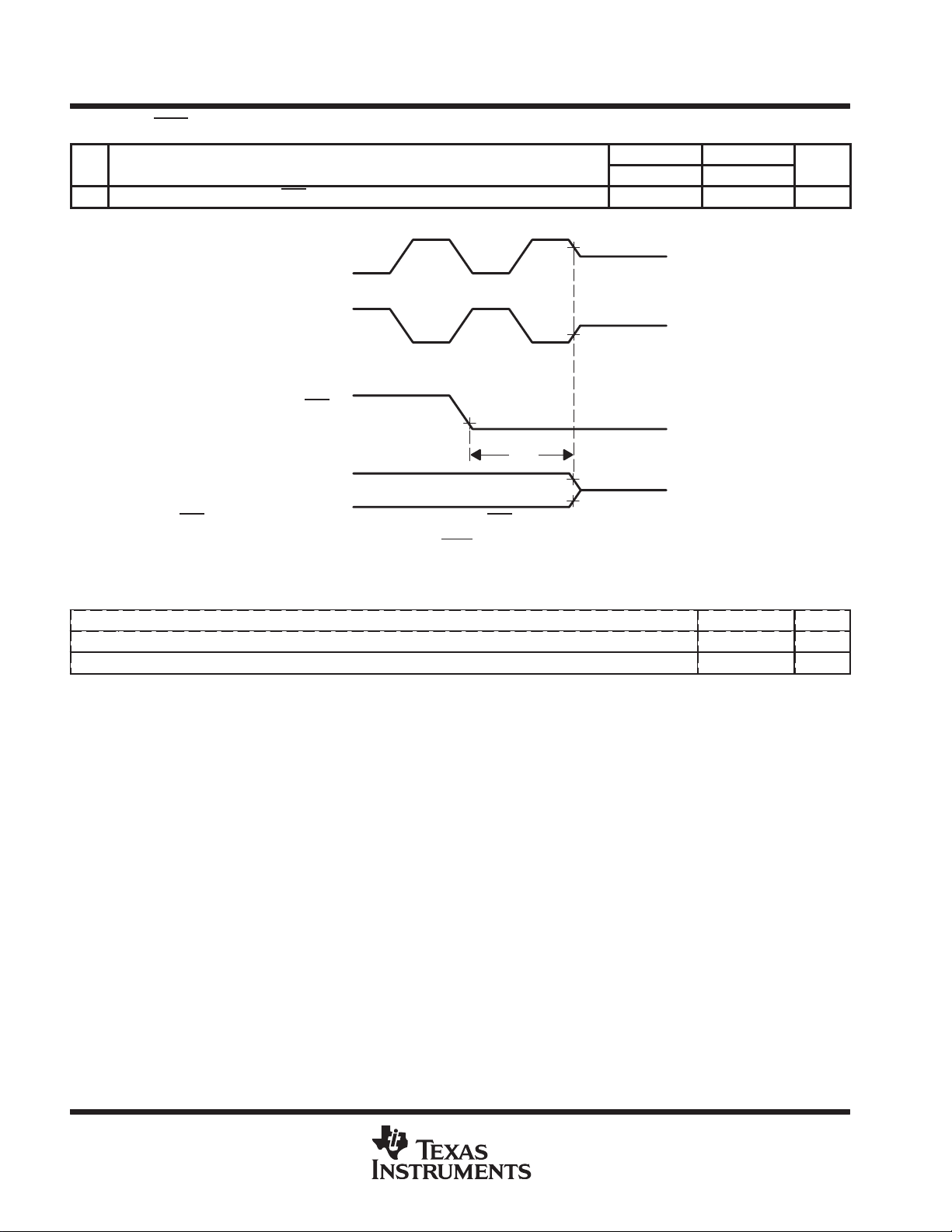
timing for INT3–INT0 interrupt response [P = t
.
61 t
su(INT)
62.1 t
w(INT)
62.2 t
†
w(INT)
Assured from characterization but not tested.
–INT0 Pin
INT3
INT3–INT0 Flag
Setup time, INT3–INT0 before H1 low 13 10 8 ns
Pulse duration of interrupt to assure only one interrupt seen
for level-triggered interrupts
Pulse duration of interrupt for edge-triggered interrupts P
H3
H1
61
62.1
62.2
] (see Figure 27)
c(H)
MIN MAX MIN MAX MIN MAX
Reset or
Interrupt
Vector Read
’C32-40 ’C32-50 ’C32-60
P 2P
†
†
P 2P
†
P
†
P 2P
†
P
Fetch First
Instruction of
Service Routine
†
ns
ns
A
Vector
Address
D
First
Instruction
Address
Figure 27. INT3–INT0 Interrupt-Response Timing
POST OFFICE BOX 1443 • HOUSTON, TEXAS 77251–1443
33

TMS320C32
NO
UNIT
DIGITAL SIGNAL PROCESSOR
SPRS027C – JANUARY 1995 – REVISED DECEMBER 1996
timing for IACK (see Notes 5 and Figure 28)
.
63 t
d(H1H-IACKL)
64 t
d(H1H-IACKH)
NOTES: 5. IACK is active for the entire duration of the bus cycle and is extended if the bus cycle utilizes wait states.
H3
H1
Delay time, H1 high to IACK low 9 7 6 ns
Delay time, H1 high to IACK high 9 7 6 ns
Fetch IACK
Instruction
Decode IACK
Instruction
IACK Data
’C32-40 ’C32-50 ’C32-60
MIN MAX MIN MAX MIN MAX
Read
IACK
63
A
D
64
Figure 28. IACK Timing
34
POST OFFICE BOX 1443 • HOUSTON, TEXAS 77251–1443

POST OFFICE BOX 1443 HOUSTON, TEXAS 77251–1443
NO
UNIT
66
t
Cycle time, CLKX/R
ns
67
t
Pulse duration, CLKX/R high/low
ns
70
t
Delay time, CLKX to DX valid
ns
71
t
Setup time, DR before CLKR low
ns
72
t
Hold time, DR from CLKR low
73
t
y,
ns
74
t
Setup time, FSR before CLKR low
ns
75
t
,
ns
76
t
,
ns
77
t
y, ,
ns
• 35
serial-port timing [P = t
] (see Figure 29 and Figure 30)
c(H)
.
65 t
d(H1-SCK)
c(SCK)
w(SCK)
68 t
r(SCK)
69 t
f(SCK)
d(DX)
su(DR)
h(DR)
d(FSX)
su(FSR)
h(FS)
su(FSX)
d(CH-DX)V
78 t
d(FSX-DX)V
79 t
d(DXZ)
†
Assured from characterization but not tested
Delay time, H1 high to internal CLKX/R high/low 13 10 8 ns
Rise time, CLKX/R 7 6 5 ns
Fall time, CLKX/R 7 6 5 ns
p
Delay time, CLKX to internal FSX
high/low
p
Hold time, FSX/R input from CLKX/R
low
Setup time, external FSX before
CLKX high
Delay time, CLKX to first DX bit, FSX
precedes CLKX high
Delay time, FSX to first DX bit, CLKX precedes FSX 30
Delay time, CLKX high to DX in the high-impedance
state following last data bit
’C32-40 ’C32-50 ’C32-60
MIN
MAX
MIN
MAX
MIN
MAX
CLKX/R ext 2.6P 2.6P 2.6P
CLKX/R int 2P (232)P 2P (232)P 2P (232)P
CLKX/R ext P + 10 P + 10 P + 10
CLKX/R int [t
c(SCK)
/2]–5 [t
C(SCK)
/2] + 5 [t
c(SCK)
/2]–5 [t
c(SCK)
/2]+5 [t
c(SCK)
/2]–5 [t
c(SCK)
/2]+5
CLKX ext 30 24 20
CLKX int 17 16 15
CLKR ext 9 9 8
CLKR int 21 17 15
CLKR ext 9 7 6 ns
CLKR int 0 0 0 ns
CLKX ext 27 22 20
CLKX int
15 15 14
CLKR ext 9 7 6
CLKR int 9 7 6
CLKX/R ext 9 7 6
CLKX/R int
CLKX ext 8 – P
CLKX int
CLKX ext 30
CLKX int
0 0 0
21–P
†
†
[t
/2]–10†8–P
c(SCK)
t
c(SCK)
/2†21–P
†
†
18
†
†
17
†
†
[t
/2]–10†8–P
c(SCK)
t
c(SCK)
†
24
†
14
†
24
†
14
/2†21–P
†
†
[t
c(SCK)
t
20
12
20
12
/2]–10
c(SCK)
†
†
†
†
/2
†
†
SPRS027C – JANuARY 1995 – REVISED DECEMBER 1996
DIGITAL SIGNAL PROCESSOR
ns
ns
TMS320C32

TMS320C32
DIGITAL SIGNAL PROCESSOR
SPRS027C – JANUARY 1995 – REVISED DECEMBER 1996
serial-port timing [P = t
65
H1
CLKX/R
DX
DR
FSR
73
FSX(INT)
FSX(EXT)
76
] (see Figure 29 and Figure 30) (continued)
c(H)
66
75
65
74
75
77
73
Bit
n-1
71
Bit
67
72
n-1
67
68
Bit
70
n-2
Bit
n-2
69
79
Bit 0
NOTES: A. Timing diagrams show operations with CLKXP = CLKRP = FSXP = FSRP = 0.
B. Timing diagrams depend upon the length of the serial-port word, where
n
= 8, 16, 24, or 32 bits, respectively.
Figure 29. Fixed Data-Rate-Mode Timing
CLKX/R
FSX(INT)
76
FSX(EXT)
DX
FSR
DR
NOTES: A. Timing diagrams show operation with CLKXP = CLKRP = FSXP = FSRP = 0.
B. Timing diagrams depend upon the length of the serial-port word, where n = 8, 16, 24, or 32 bits, respectively.
C. The timings that are not specified expressly for the variable data-rate mode are the same as those that are specified
for the fixed data-rate mode.
71
74
77
73
Bit
n-1
78
Bit
75
n-1
72
70
Bit
n-2
Bit
n-2
Bit
n-3
Bit
n-3
79
Bit 0
36
Figure 30. Variable Data-Rate-Mode Timing
POST OFFICE BOX 1443 • HOUSTON, TEXAS 77251–1443

NO
UNIT
TMS320C32
DIGITAL SIGNAL PROCESSOR
SPRS027C – JANUARY 1995 – REVISED DECEMBER 1996
timing for HOLD/HOLDA [P = t
.
80 t
su(HOLD)
81 t
v(HOLDA)
82 t
w(HOLD)
83 t
w(HOLDA)
84 t
d(H1L-SH)H
84.1 t
d(H1H-IOS)H
85 t
dis(H1L-S)
86 t
en(H1L-S)
87 t
dis(H1L-RW)
88 t
en(H1L-RW)
89 t
dis(H1L-A)
90 t
en(H1L-A)
91 t
dis(H1H-D)
†
Assured from characterization but not tested
‡
Not tested
NOTE 6: HOLD
sequence shown occurs; otherwise, an additional delay of one clock cycle can occur. The NOHOLD bit of the primary-bit-control register
overwrites the HOLD
Setup time, HOLD before H1 low 13 10 8 ns
Valid time, HOLDA after H1 low 0
Pulse duration, HOLD low 2P 2P 2P ns
Pulse duration, HOLDA low P–5
Delay time, H1 low to STRBx high for a HOLD 0
Delay time, H1 high to IOSTRB high for a HOLD 0
Disable time, H1 low to STRBx or IOSTRB (in the
high-impedance state)
Enable time, H1 low to STRBx or IOSTRB active 0
Disable time, H1 low to R/W in the
high-impedance state
Enable time, H1 low to R/W (active) 0
Disable time, H1 low to A in the high-impedance
state
Enable time, H1 low to A valid 0
Disable time, H1 high to D disabled in the
high-impedance state
is an asynchronous input and can be asserted at any point during a clock cycle. If the specified timings are met, the exact
signal.
] (see Note 6 and Figure 31)
c(H)
’C32-40 ’C32-50 ’C32-60
MIN MAX MIN MAX MIN MAX
†
†
‡
‡
‡
0
‡
†
0
†
‡
0
‡
‡
0
9 0
9 0
9 0
†
9
9 0
†
9
9 0
†
10
13 0
†
9
P–5
†
†
‡
‡
‡
0
‡
†
0
†
‡
0
‡
‡
0
7 0
7 0
7 0
†
8
7 0
†
8
7 0
†
8
12 0
†
8
P–5
†
†
‡
‡
‡
0
‡
†
0
†
‡
0
‡
‡
0
6 ns
6 ns
6 ns
†
7
6 ns
†
7
6 ns
†
7
11 ns
†
7
ns
ns
ns
ns
ns
POST OFFICE BOX 1443 • HOUSTON, TEXAS 77251–1443
37

TMS320C32
DIGITAL SIGNAL PROCESSOR
SPRS027C – JANUARY 1995 – REVISED DECEMBER 1996
timing for HOLD/HOLDA [P = t
H3
H1
80
HOLD
HOLDA
(see Note A)
STRBx
84.1
IOSTRB
R/W
A
D
NOTE A: HOLDA goes low in response to HOLD going low and continues to remain low until one H1 cycle after HOLD goes back high.
84
Write Data
] (see Note 6 and Figure 31) (continued)
c(H)
82
81
85
85 86
87
89
91
80
83
81
86
88
90
Figure 31. HOLD/HOLDA Timing
38
POST OFFICE BOX 1443 • HOUSTON, TEXAS 77251–1443

NO
UNIT
NO
UNIT
TMS320C32
DIGITAL SIGNAL PROCESSOR
SPRS027C – JANUARY 1995 – REVISED DECEMBER 1996
timing of peripheral pin configured as general-purpose I/O (see Figure 32)
.
92 t
su(GPIOH1L)
93 t
h(GPIOH1L)
94 t
d(GPIOH1H)
H3
H1
Peripheral Pin
(see Note A)
NOTE A: Peripheral pins include CLKX0, CLKR0, DX0, DR0, FSX0, FSR0, and TCLKx. The modes of these pins are defined by the contents
of internal control registers associated with each peripheral.
Setup time, general-purpose input before H1 low 10 9 8 ns
Hold time, general-purpose input after H1 low 0 0 0 ns
Delay time, general-purpose output after H1 high 13 10 8 ns
93
92
Figure 32. Peripheral-Pin General-Purpose I/O Timing
’C32-40 ’C32-50 ’C32-60
MIN MAX MIN MAX MIN MAX
94
94
timing of peripheral pin changing from general-purpose output to input mode (see Figure 33)
.
95 t
h(H1H)
96 t
su(GPI0H1L)
97 t
h(GPIOH1L)
H3
H1
Control Bit
Peripheral Pin
(see Note A)
I/O
Data Bit
Hold time, after H1 high 13 12 11 ns
Setup time, peripheral pin before H1 low 10 9 8 ns
Hold time, peripheral pin after H1 low 0 0 0 ns
Execute Store
of Peripheral
Control
Register
95
Output
Buffers
Go From
Output to Input
96
’C32-40 ’C32-50 ’C32-60
MIN MAX MIN MAX MIN MAX
Value on
Pin Seen
Synchronizer Delay
97
in
Peripheral
Control Register
Data Sampled
NOTE A: Peripheral pins include CLKX0, CLKR0, DX0, DR0, FSX0, FSR0, and TCLKx. The modes of these pins are defined by the contents
of internal control registers associated with each peripheral.
Data
Seen
Figure 33. Timing of Peripheral Pin Changing From General-Purpose Output to Input-Mode
POST OFFICE BOX 1443 • HOUSTON, TEXAS 77251–1443
39

TMS320C32
NO
UNIT
DIGITAL SIGNAL PROCESSOR
SPRS027C – JANUARY 1995 – REVISED DECEMBER 1996
timing of peripheral pin changing from general-purpose input to output mode (see Figure 34)
.
98 t
d(GPIOH1H)
H3
H1
I/O Control Bit
Delay time, H1 high to peripheral pin switching from input
to output
Execution of Store of
Peripheral Control
Register
’C32-40 ’C32-50 ’C32-60
MIN MAX MIN MAX MIN MAX
13 10 8 ns
98
Peripheral Pin
(see Note A)
NOTE A: Peripheral pins include CLKX0, CLKR0, DX0, DR0, FSX0, FSR0, and TCLKx. The modes of these pins are defined by the contents
of internal control registers associated with each peripheral.
Figure 34. Timing of Peripheral Pin Changing From General-Purpose Input to Output Mode
40
POST OFFICE BOX 1443 • HOUSTON, TEXAS 77251–1443

NO
UNIT
102
t
Cycle time, TCLK
ns
103
t
Pulse duration, TCLK high/lo
ns
NO
UNIT
102
t
Cycle time, TCLK cycle time
ns
103
t
Pulse duration, TCLK high / lo
ns
NO
UNIT
102
t
Cycle time, TCLK cycle time
ns
103
t
Pulse duration, TCLK high/lo
ns
TMS320C32
DIGITAL SIGNAL PROCESSOR
SPRS027C – JANUARY 1995 – REVISED DECEMBER 1996
timing for timer pin [P = t
.
99 t
su(TCLKH1L)
100 t
h(TCLKH1L)
101 t
d(TCLKH1H)
c(TCLK)
w(TCLK)
†
Timing parameters 99 and 100 are applicable for a synchronous input clock. T iming parameters 102 and 103 are applicable for an asynchronous
input clock.
‡
Assured by design but not tested
.
99 t
su(TCLKH1L)
100 t
h(TCLKH1L)
101 t
d(TCLKH1H)
c(TCLK)
w(TCLK)
†
Timing parameters 99 and 100 are applicable for a synchronous input clock. T iming parameters 102 and 103 are applicable for an asynchronous
input clock.
‡
Assured by design but not tested
.
99 t
su(TCLKH1L)
100 t
h(TCLKH1L)
101 t
d(TCLKH1H)
c(TCLK)
w(TCLK)
†
Timing parameters 99 and 100 are applicable for a synchronous input clock. T iming parameters 102 and 103 are applicable for an asynchronous
input clock.
‡
Assured by design but not tested
Setup time, TCLK external before H1 low 10 ns
Hold time, TCLK external after H1 low 0 ns
Delay time, H1 high to TCLK internal valid 9 ns
Setup time, TCLK external before H1 low 8 ns
Hold time, TCLK external after H1 low 0 ns
Delay time, H1 high to TCLK internal valid 9 ns
Setup time, TCLK external before H1 low 6 ns
Hold time, TCLK external after H1 low 0 ns
Delay time, H1 high to TCLK internal valid 8 ns
] (see Figure 35)
c(H)
w
w
w
†
’C32-40
MIN MAX
TCLK external 2.6P
TCLK internal 2P (232)P
TCLK external P + 10
TCLK internal [t
TCLK external 2.6P
TCLK internal 2P (232)P
TCLK external P + 10
TCLK internal [t
TCLK external 2.6P
TCLK internal 2P (232)P
TCLK external P + 10
TCLK internal [t
c(TCLK)
c(TCLK)
c(TCLK)
/2]–5 [t
MIN MAX
/2]–5 [t
MIN MAX
/2]–5 [t
c(TCLK)
’C32-50
c(TCLK)
’C32-60
c(TCLK)
‡
/2]+5
‡
/2]+5
‡
/2]+5
H3
H1
TCLKx
99
100
101
103
102
Figure 35. Timing for Timer Pin
POST OFFICE BOX 1443 • HOUSTON, TEXAS 77251–1443
101
41
TMS320C32
UNIT
DIGITAL SIGNAL PROCESSOR
SPRS027C – JANUARY 1995 – REVISED DECEMBER 1996
timing for SHZ pin [Q = t
NO. MIN MAX MIN MAX
104 t
†
NOTE A: Enabling SHZ destroys ’C32 register and memory contents. Assert SHZ = 1 and reset the ’C32 to restore it to a known condition.
dis(SHZ)
Assured by characterization but not tested
Disable time, SHZ low to all O, I/O pins in the high-impedance state 0†2Q
] (see Figure 36)
c(CI)
H3
H1
(see Note A)
SHZ
All I/O Pins
104
’C32-50
†
†
’C32-60
0†2Q
†
Figure 36. SHZ Pin Timing
ns
R
R
Table 1. Thermal Resistance Characteristics for PCM package
PARAMETER MIN MAX UNIT
Junction-to-free-air 39 °C/W
ΘJA
Junction-to-case 10.0 °C/W
ΘJC
42
POST OFFICE BOX 1443 • HOUSTON, TEXAS 77251–1443

TMS320C32
DIGITAL SIGNAL PROCESSOR
SPRS027C – JANUARY 1995 – REVISED DECEMBER 1996
MECHANICAL DATA
PCM(S-PQFP-G***) PLASTIC QUAD FLATPACK
144 PIN SHOWN
108 73
109
144
72
37
136
A
28,20
SQ
27,80
31,45
SQ
30,95
0,38
0,22
0,65 TYP
NO. OF PINS*** A
144
160
3,60
3,20
0,25 MIN
0,13
M
22,75 TYP
25,35 TYP
0,16 NOM
0°–7°
4,10 MAX
NOTES: A. All linear dimensions are in millimeters.
B. This drawing is subject to change without notice.
C. Falls within JEDEC MS-022
D. The 144PCM is identical to 160PCM except that 4 leads per corner are removed.
E. Foot length is measured from lead tip to a position on backside of lead 0,25 mm above seating plane (gage plane)
F. Preliminary drawing
POST OFFICE BOX 1443 • HOUSTON, TEXAS 77251–1443
1,03
0,73
Seating Plane
0,10
(see Note C)
4040015/A–10/93
43

IMPORTANT NOTICE
T exas Instruments and its subsidiaries (TI) reserve the right to make changes to their products or to discontinue
any product or service without notice, and advise customers to obtain the latest version of relevant information
to verify, before placing orders, that information being relied on is current and complete. All products are sold
subject to the terms and conditions of sale supplied at the time of order acknowledgement, including those
pertaining to warranty, patent infringement, and limitation of liability.
TI warrants performance of its semiconductor products to the specifications applicable at the time of sale in
accordance with TI’s standard warranty. Testing and other quality control techniques are utilized to the extent
TI deems necessary to support this warranty . Specific testing of all parameters of each device is not necessarily
performed, except those mandated by government requirements.
CERTAIN APPLICA TIONS USING SEMICONDUCT OR PRODUCTS MAY INVOLVE POTENTIAL RISKS OF
DEATH, PERSONAL INJURY, OR SEVERE PROPERTY OR ENVIRONMENTAL DAMAGE (“CRITICAL
APPLICATIONS”). TI SEMICONDUCTOR PRODUCTS ARE NOT DESIGNED, AUTHORIZED, OR
WARRANTED TO BE SUITABLE FOR USE IN LIFE-SUPPORT DEVICES OR SYSTEMS OR OTHER
CRITICAL APPLICA TIONS. INCLUSION OF TI PRODUCTS IN SUCH APPLICATIONS IS UNDERST OOD TO
BE FULLY AT THE CUSTOMER’S RISK.
In order to minimize risks associated with the customer’s applications, adequate design and operating
safeguards must be provided by the customer to minimize inherent or procedural hazards.
TI assumes no liability for applications assistance or customer product design. TI does not warrant or represent
that any license, either express or implied, is granted under any patent right, copyright, mask work right, or other
intellectual property right of TI covering or relating to any combination, machine, or process in which such
semiconductor products or services might be or are used. TI’s publication of information regarding any third
party’s products or services does not constitute TI’s approval, warranty or endorsement thereof.
Copyright 1998, Texas Instruments Incorporated
 Loading...