

Page 1

TMS320C2xx
User’s Guide
Manufacturing Part Number: D412008-9761 revision A
Literature Number: SPRU127B
January 1997
Printed on Recycled Paper
Page 2

IMPORTANT NOTICE
T exas Instruments (TI) reserves the right to make changes to its products or to discontinue any
semiconductor product or service without notice, and advises its customers to obtain the latest
version of relevant information to verify , before placing orders, that the information being relied
on is current.
TI warrants performance of its semiconductor products and related software to the specifications
applicable at the time of sale in accordance with TI’s standard warranty . T esting and other quality
control techniques are utilized to the extent TI deems necessary to support this warranty.
Specific testing of all parameters of each device is not necessarily performed, except those
mandated by government requirements.
Certain applications using semiconductor products may involve potential risks of death,
personal injury , or severe property or environmental damage (“Critical Applications”).
TI SEMICONDUCTOR PRODUCTS ARE NOT DESIGNED, INTENDED, AUTHORIZED, OR
WARRANTED TO BE SUITABLE FOR USE IN LIFE-SUPPORT APPLICATIONS, DEVICES
OR SYSTEMS OR OTHER CRITICAL APPLICATIONS.
Inclusion of TI products in such applications is understood to be fully at the risk of the customer.
Use of TI products in such applications requires the written approval of an appropriate TI officer .
Questions concerning potential risk applications should be directed to TI through a local SC
sales office.
In order to minimize risks associated with the customer’s applications, adequate design and
operating safeguards should be provided by the customer to minimize inherent or procedural
hazards.
TI assumes no liability for applications assistance, customer product design, software
performance, or infringement of patents or services described herein. Nor does TI warrant or
represent that any license, either express or implied, is granted under any patent right, copyright,
mask work right, or other intellectual property right of TI covering or relating to any combination,
machine, or process in which such semiconductor products or services might be or are used.
Copyright 1996, Texas Instruments Incorporated
Page 3

About This Manual
How to Use This Manual
Preface
Read This First
This user’s guide describes the architecture, hardware, assembly language
instructions, and general operation of the TMS320C2xx digital signal
processors (DSPs). This manual can also be used as a reference guide for
developing hardware and/or software applications. In this document, ’C2xx
refers to any of the TMS320C2xx devices, except where device-specific
information is explicitly stated. When device-specific information is given, the
device name may be abbreviated; for example, TMS320C203 will be
abbreviated as ’C203.
How to Use This Manual
Chapter 1,
introduces the key features of the TMS320C2xx generation of that family.
Chapter 2,
providing information about the CPU, bus structure, memory, on-chip
peripherals, and scanning logic.
If you are reading this manual to learn about the ’C209, Chapter 1 1 is important
for you. There are some notable differences between the ’C209 and other
’C2xx devices, and Chapter 1 1 explains these differences. In addition, it shows
how to use this manual to get a complete picture of the ’C209.
The following table points you to major topics.
Introduction
Architectural Overview
, summarizes the TMS320 family of products and then
, summarizes the ’C2xx architecture,
iii
Page 4

How to Use This Manual
For this information: Look here:
Addressing modes (for addressing data
memory)
Assembly language instructions Chapter 7,
Chapter 6,
Instructions
Assembly language instructions of
TMS320C1x, ’C2x, ’C2xx, and ’C5x
compared
Boot loader Chapter 4,
Clock generator Chapter 8,
CPU Chapter 3,
Custom ROM from TI Appendix D,
Appendix B,
TMS320C1x/C2x/C2xx/C5x
Instruction Set Comparison
to TI
Emulator Appendix E,
Using XDS510 Emulator
Features Chapter 1,
Chapter 2,
Input/output ports Chapter 4,
Interrupts Chapter 5,
Memory configuration Chapter 4,
Memory interfacing Chapter 4,
On-chip peripherals Chapter 8,
Pipeline Chapter 5,
Program control Chapter 5,
Program examples Appendix C,
Program-memory address generation Chapter 5,
Registers summarized Appendix A,
Serial ports Chapter 9,
Chapter 10,
Stack Chapter 5,
Status registers Chapter 5,
Timer Chapter 8,
TMS320C209 differences and
similarities
Wait-state generator Chapter 8,
Chapter 1 1,
Addressing Modes
Assembly Language
Memory and I/O Spaces
On-Chip Peripherals
Central Processing Unit
Submitting ROM Codes
Design Considerations for
Introduction
Architectural Overview
Memory and I/O Spaces
Program Control
Memory and I/O Spaces
Memory and I/O Spaces
On-Chip Peripherals
Program Control
Program Control
Program Examples
Program Control
Register Summary
Synchronous Serial Port
Asynchronous Serial Port
Program Control
Program Control
On-Chip Peripherals
TMS320C209
On-Chip Peripherals
iv
Page 5

Notational Conventions
This document uses the following conventions:
-
-
Notational Conventions/Information About Cautions
Program listings and program examples are shown in a special
typeface.
Here is a segment of a program listing:
OUTPUT LDP #6 ;select data page 6
BLDD #300, 20h ;move data at address 300h to 320h
RET
In syntax descriptions, bold portions of a syntax should be entered as
shown;
italic
portions of a syntax identify information that you specify . Here
is an example of an instruction syntax:
BLDD
BLDD is the instruction mnemonic, which must be typed as shown. You
specify the two parameters,
-
Square brackets ( [ and ] ) identify an optional parameter. If you use an
optional parameter, you specify the information within the brackets; you
do not type the brackets themselves. Y ou separate each optional operand
from required operands with a comma and a space. Here is a sample
syntax:
BLDD
BLDD is the instruction. The two required operands are
destination
you choose to use AR
a chosen value for
BLDD *, #310h, AR3
Information About Cautions
This book contains cautions.
This is an example of a caution statement.
A caution statement describes a situation that could potentially
damage your software or equipment.
source, destination
source
and
source, destination
destination
[, ARn]
.
source
, and the optional operand is ARn. AR is bold and n is italic; if
n
, you must type the letters A and R and then supply
n
(in this case, a value from 0 to 7). Here is an example:
and
The information in a caution is provided for your protection. Please read each
caution carefully.
Read This First
v
Page 6

Related Documentation From Texas Instruments
Related Documentation From Texas Instruments
This subsection describes related TI documents that can be ordered by
calling the T exas Instruments Literature Response Center at (800) 477–8924.
When ordering, please identify the document by its title and literature number.
The following data sheets contain the electrical and timing specifications for
the TMS320C2xx devices, as well as signal descriptions and pinouts for all of
the available packages:
-
TMS320C2xx data sheet (literature number SPRS025)
-
TMS320F2xx data sheet (literature number SPRS050). This data sheet
covers the TMS320C2xx devices that have on-chip flash memory.
The books listed below provide additional information about using the
TMS320C2xx devices and related support tools, as well as more general
information about using the TMS320 family of DSPs.
TMS320C1x/C2x/C2xx/C5x Code Generation Tools Getting Started
Guide
TMS320C1x, TMS320C2x, TMS320C2xx, and TMS320C5x assembly
language tools and the C compiler for the ’C1x, ’C2x, ’C2xx, and ’C5x
devices. The installation for MS-DOS, OS/2, SunOS, and Solaris
systems is covered.
TMS320C1x/C2x/C2xx/C5x Assembly Language Tools User’s Guide
(literature number SPRU018) describes the assembly language tools
(assembler, linker, and other tools used to develop assembly language
code), assembler directives, macros, common object file format, and
symbolic debugging directives for the ’C1x, ’C2x, ’C2xx, and ’C5x
generations of devices.
TMS320C2x/C2xx/C5x Optimizing C Compiler User’s Guide
number SPRU024) describes the ’C2x/C2xx/C5x C compiler. This C
compiler accepts ANSI standard C source code and produces TMS320
assembly language source code for the ’C2x, ’C2xx, and ’C5x
generations of devices.
(literature number SPRU121) describes how to install the
(literature
TMS320C2xx C Source Debugger User’s Guide
(literature number
SPRU151) tells you how to invoke the ’C2xx emulator and simulator
versions of the C source debugger interface. This book discusses
various aspects of the debugger interface, including window
management, command entry , code execution, data management, and
breakpoints. It also includes a tutorial that introduces basic debugger
functionality.
vi
Page 7

Related Documentation From Texas Instruments
TMS320C2xx Simulator Getting Started
(literature number SPRU137)
describes how to install the TMS320C2xx simulator and the C source
debugger for the ’C2xx. The installation for MS-DOS, PC-DOS,
SunOS, Solaris, and HP-UX systems is covered.
TMS320C2xx Emulator Getting Started Guide
(literature number
SPRU209) tells you how to install the Windows 3.1 and Windows 95
versions of the ’C2xx emulator and C source debugger interface.
XDS51x Emulator Installation Guide
(literature number SPNU070)
describes the installation of the XDS510, XDS510PP, and
XDS510WS emulator controllers. The installation of the XDS511
emulator is also described.
JT AG/MPSD Emulation Technical Reference
(literature number SPDU079)
provides the design requirements of the XDS510 emulator controller.
Discusses JTAG designs (based on the IEEE 1149.1 standard) and
modular port scan device (MPSD) designs.
TMS320 DSP Development Support Reference Guide
(literature number
SPRU011) describes the TMS320 family of digital signal processors and
the tools that support these devices. Included are code-generation tools
(compilers, assemblers, linkers, etc.) and system integration and debug
tools (simulators, emulators, evaluation modules, etc.). Also covered are
available documentation, seminars, the university program, and factory
repair and exchange.
Digital Signal Processing Applications with the TMS320 Family,
Volumes 1, 2, and 3
(literature numbers SPRA012, SPRA016,
SPRA017) Volumes 1 and 2 cover applications using the ’C10 and ’C20
families of fixed-point processors. Volume 3 documents applications
using both fixed-point processors as well as the ’C30 floating-point
processor.
TMS320 DSP Designer’s Notebook: Volume 1
.
SPRT125)
’C3x, ’C4x, ’C5x, and other TI DSPs
Presents solutions to common design problems using ’C2x,
.
TMS320 Third-Party Support Reference Guide
(literature number
(literature number
SPRU052) alphabetically lists over 100 third parties that provide various
products that serve the family of ’320 digital signal processors. A myriad
of products and applications are offered—software and hardware
development tools, speech recognition, image processing, noise
cancellation, modems, etc.
Read This First
vii
Page 8

Related Articles
Related Articles
“A Greener World Through DSP Controllers”, Panos Papamichalis,
Multimedia Technology
“A Single-Chip Multiprocessor DSP for Image Processing—TMS320C80”,
Dr. Ing. Dung Tu,
“Application Guide with DSP Leading-Edge Technology”, Y. Nishikori, M.
Hattori, T. Fukuhara, R.Tanaka, M. Shimoda, I. Kudo, A.Yanagitani, H.
Miyaguchi, et al.,
“Approaching the No-Power Barrier”, Jon Bradley and Gene Frantz,
Design
“Beware of BAT: DSPs Add Brilliance to New Weapons Systems”, Panos
Papamichalis,
“Choose DSPs for PC Signal Processing”, Panos Papamichalis,
, January 9, 1995.
DSP & Multimedia Technology
Multimedia Technology
“Developing Nations Take Shine to Wireless”, Russell MacDonald, Kara
Schmidt and Kim Higden,
“Digital Signal Processing Solutions T arget V ertical Application Markets”, Ron
ECN
Wages,
“Digital Signal Processors Boost Drive Performance”, Tim Adcock,
Storage
, September 1995.
, September/October 1995.
, September 1994.
Industrie Elektronik
, Germany, March 1995.
Electronics Engineering
, January/February 1995.
EE Times
, October 2, 1995.
, November 1995.
, October 1994.
DSP &
Electronic
DSP &
Data
viii
“DSP and Speech Recognition, An Origin of the Species”, Panos
Papamichalis,
“DSP Design Takes Top-Down Approach”, Andy Fritsch and Kim Asal,
Series Part III
“DSPs Advance Low-Cost ‘Green’ Control”, Gregg Bennett,
II
,
EE Times
“DSPs Do Best on Multimedia Applications”, Doug Rasor,
World
, October 9–16, 1995.
“DSPs: Speech Recognition Technology Enablers”, Gene Frantz and Gregg
Bennett,
“Easing JTAG Testing of Parallel-Processor Projects”, Tony Coomes, Andy
Fritsch, and Reid Tatge,
November 1995.
DSP & Multimedia Technology
,
EE Times
, April 17, 1995.
I&CS
, May 1995.
, July 17, 1995.
Asian Electronics Engineer
, July 1994.
DSP
DSP Series Part
Asian Computer
, Manila, Philippines,
Page 9

Related Articles
“Fixed or Floating? A Pointed Question in DSPs”, Jim Larimer and Daniel
EDN
Chen,
“Function-Focused Chipsets: Up the DSP Integration Core”, Panos
Papamichalis,
, August 3, 1995.
DSP & Multimedia Technology
, March/April 1995.
“GSM: Standard, Strategien und Systemchips”, Edgar Auslander,
Praxis
, Germany, October 6, 1995.
“High T ech Copiers to Improve Images and Reduce Paperwork”, Karl Guttag,
Document Management
“Host-Enabled Multimedia: Brought to You by DSP Solutions”, Panos
Papamichalis,
“Integration Shrinks Digital Cellular Telephone Designs”, Fred Cohen and
Mike McMahan,
“On-Chip Multiprocessing Melds DSPs”, Karl Guttag and Doug Deao,
Series Part III
“Real-Time Control”, Gregg Bennett,
“Speech Recognition”, P.K. Rajasekaran and Mike McMahan,
DSP & Multimedia Technology
Wireless System Design
,
EE Times
Design & Development
“Telecom Future Driven by Reduced Milliwatts per DSP Function”, Panos
Papamichalis,
“The Digital Signal Processor Development Environment”, Greg Peake,
DSP & Multimedia Technology
Embedded System Engineering
, July/August 1995.
, September/October 1995.
, November 1994.
, July 18, 1994.
Appliance Manufacturer
, May 1995.
, May/June 1995.
, United Kingdom, February 1995.
Elektronik
DSP
, May 1995.
Wireless
“The Growing Spectrum of Custom DSPs”, Gene Frantz and Kun Lin,
,
Series Part II
“The Wide World of DSPs, ” Jim Larimer,
“Third-Party Support Drives DSP Development for Uninitiated and Experts
Alike”, Panos Papamichalis,
1994/January 1995.
“Toward an Era of Economical DSPs”, John Cooper,
Times
, Jan. 23, 1995.
EE Times
, April 18, 1994.
DSP & Multimedia Technology
Design News
Read This First
, June 27, 1994.
, December
DSP Series Part I, EE
DSP
ix
Page 10

Trademarks
Trademarks
TI, 320 Hotline On-line, XDS510, XDS510PP, XDS510WS, and XDS511 are
trademarks of Texas Instruments Incorporated.
HP-UX is a trademark of Hewlett-Packard Company.
Intel is a trademark of Intel Corporation.
MS-DOS and Windows are registered trademarks of Microsoft Corporation.
PAL
is a registered trademark of Advanced Micro Devices, Inc.
OS/2, PC, and PC-DOS are trademarks of International Business Machines
Corporation.
Solaris and SunOS are trademarks of Sun Microsystems, Inc.
x
Page 11
If Y ou Need Assistance
If You Need Assistance. . .
-
World-Wide Web Sites
TI Online http://www.ti.com
Semiconductor Product Information Center (PIC) http://www.ti.com/sc/docs/pic/home.htm
DSP Solutions http://www.ti.com/dsps
320 Hotline On-line
-
North America, South America, Central America
Product Information Center (PIC) (972) 644-5580
TI Literature Response Center U.S.A. (800) 477-8924
Software Registration/Upgrades (214) 638-0333 Fax: (214) 638-7742
U.S.A. Factory Repair/Hardware Upgrades (281) 274-2285
U.S. T echnical T raining Organization (972) 644-5580
DSP Hotline (281) 274-2320 Fax: (281) 274-2324 Email: dsph@ti.com
DSP Modem BBS (281) 274-2323
DSP Internet BBS via anonymous ftp to ftp://ftp.ti.com/mirrors/tms320bbs
-
Europe, Middle East, Africa
European Product Information Center (EPIC) Hotlines:
Multi-Language Support +33 1 30 70 11 69 Fax: +33 1 30 70 10 32 Email: epic@ti.com
Deutsch +49 8161 80 33 11 or +33 1 30 70 11 68
English +33 1 30 70 11 65
Francais +33 1 30 70 11 64
Italiano +33 1 30 70 11 67
EPIC Modem BBS +33 1 30 70 11 99
European Factory Repair +33 4 93 22 25 40
Europe Customer Training Helpline Fax: +49 81 61 80 40 10
t
http://www.ti.com/sc/docs/dsps/support.html
-
Asia-Pacific
Literature Response Center +852 2 956 7288 Fax: +852 2 956 2200
Hong Kong DSP Hotline +852 2 956 7268 Fax: +852 2 956 1002
Korea DSP Hotline +82 2 551 2804 Fax: +82 2 551 2828
Korea DSP Modem BBS +82 2 551 2914
Singapore DSP Hotline Fax: +65 390 7179
Taiwan DSP Hotline +886 2 377 1450 Fax: +886 2 377 2718
Taiwan DSP Modem BBS +886 2 376 2592
Taiwan DSP Internet BBS via anonymous ftp to ftp://dsp.ee.tit.edu.tw/pub/TI/
-
Japan
Product Information Center +0120-81-0026 (in Japan) Fax: +0120-81-0036 (in Japan)
DSP Hotline +03-3769-8735 or
DSP BBS via Nifty-Serve Type “Go TIASP”
-
Documentation
When making suggestions or reporting errors in documentation, please include the following information that is on the title
page: the full title of the book, the publication date, and the literature number.
Mail: Texas Instruments Incorporated Email: comments@books.sc.ti.com
Technical Documentation Services, MS 702
P.O. Box 1443
Houston, Texas 77251-1443
Note: When calling a Literature Response Center to order documentation, please specify the literature number of the
book.
+03-3457-0972 or (INTL) 813-3457-0972 Fax: +03-3457-1259 or (INTL) 813-3457-1259
(INTL) 813-3769-8735 Fax: +03-3457-7071 or (INTL) 813-3457-7071
Read This First
xi
Page 12

Contents
Contents
1 Introduction 1-1. . . . . . . . . . . . . . . . . . . . . . . . . . . . . . . . . . . . . . . . . . . . . . . . . . . . . . . . . . . . . . . . . . . . .
Summarizes the features of the TMS320 family of products and presents typical applications.
Describes the TMS320C2xx DSP and lists its key features.
1.1 TMS320 Family 1-2. . . . . . . . . . . . . . . . . . . . . . . . . . . . . . . . . . . . . . . . . . . . . . . . . . . . . . . . . . . .
1.1.1 History, Development, and Advantages of TMS320 DSPs 1-2. . . . . . . . . . . . . . . . .
1.1.2 Typical Applications for the TMS320 Family 1-4. . . . . . . . . . . . . . . . . . . . . . . . . . . . .
1.2 TMS320C2xx Generation 1-5. . . . . . . . . . . . . . . . . . . . . . . . . . . . . . . . . . . . . . . . . . . . . . . . . . . .
1.3 Key Features of the TMS320C2xx 1-6. . . . . . . . . . . . . . . . . . . . . . . . . . . . . . . . . . . . . . . . . . . .
2 Architectural Overview 2-1. . . . . . . . . . . . . . . . . . . . . . . . . . . . . . . . . . . . . . . . . . . . . . . . . . . . . . . . . . .
Summarizes the TMS320C2xx architecture. Provides information about the CPU, bus
structure, memory, on-chip peripherals, and scanning logic.
2.1 ’C2xx Bus Structure 2-3. . . . . . . . . . . . . . . . . . . . . . . . . . . . . . . . . . . . . . . . . . . . . . . . . . . . . . . . .
2.2 Central Processing Unit 2-5. . . . . . . . . . . . . . . . . . . . . . . . . . . . . . . . . . . . . . . . . . . . . . . . . . . . .
2.2.1 Central Arithmetic Logic Unit (CALU) and Accumulator 2-5. . . . . . . . . . . . . . . . . . .
2.2.2 Scaling Shifters 2-5. . . . . . . . . . . . . . . . . . . . . . . . . . . . . . . . . . . . . . . . . . . . . . . . . . . . .
2.2.3 Multiplier 2-6. . . . . . . . . . . . . . . . . . . . . . . . . . . . . . . . . . . . . . . . . . . . . . . . . . . . . . . . . . .
2.2.4 Auxiliary Register Arithmetic Unit (ARAU) and Auxiliary Registers 2-6. . . . . . . . . .
2.3 Memory and I/O Spaces 2-7. . . . . . . . . . . . . . . . . . . . . . . . . . . . . . . . . . . . . . . . . . . . . . . . . . . . .
2.3.1 Dual-Access On-Chip RAM 2-7. . . . . . . . . . . . . . . . . . . . . . . . . . . . . . . . . . . . . . . . . . .
2.3.2 Single-Access On-Chip Program/Data RAM 2-8. . . . . . . . . . . . . . . . . . . . . . . . . . . .
2.3.3 Factory-Masked On-Chip ROM 2-8. . . . . . . . . . . . . . . . . . . . . . . . . . . . . . . . . . . . . . . .
2.3.4 Flash Memory 2-9. . . . . . . . . . . . . . . . . . . . . . . . . . . . . . . . . . . . . . . . . . . . . . . . . . . . . . .
2.4 Program Control 2-10. . . . . . . . . . . . . . . . . . . . . . . . . . . . . . . . . . . . . . . . . . . . . . . . . . . . . . . . . . .
2.5 On-Chip Peripherals 2-11. . . . . . . . . . . . . . . . . . . . . . . . . . . . . . . . . . . . . . . . . . . . . . . . . . . . . . .
2.5.1 Clock Generator 2-11. . . . . . . . . . . . . . . . . . . . . . . . . . . . . . . . . . . . . . . . . . . . . . . . . . . .
2.5.2 CLKOUT1-Pin Control (CLK) Register 2-11. . . . . . . . . . . . . . . . . . . . . . . . . . . . . . . . .
2.5.3 Hardware Timer 2-11. . . . . . . . . . . . . . . . . . . . . . . . . . . . . . . . . . . . . . . . . . . . . . . . . . . .
2.5.4 Software-Programmable Wait-State Generator 2-11. . . . . . . . . . . . . . . . . . . . . . . . .
2.5.5 General-Purpose I/O Pins 2-12. . . . . . . . . . . . . . . . . . . . . . . . . . . . . . . . . . . . . . . . . . .
2.5.6 Serial Ports 2-12. . . . . . . . . . . . . . . . . . . . . . . . . . . . . . . . . . . . . . . . . . . . . . . . . . . . . . . .
2.6 Scanning-Logic Circuitry 2-13. . . . . . . . . . . . . . . . . . . . . . . . . . . . . . . . . . . . . . . . . . . . . . . . . . . .
xiii
Page 13

Contents
3 Central Processing Unit 3-1. . . . . . . . . . . . . . . . . . . . . . . . . . . . . . . . . . . . . . . . . . . . . . . . . . . . . . . . . .
Describes the TMS320C2xx CPU. Includes information about the central arithmetic logic unit,
the accumulator, the shifters, the multiplier , and the auxiliary register arithmetic unit. Concludes
with a description of the status register bits.
3.1 Input Scaling Section 3-3. . . . . . . . . . . . . . . . . . . . . . . . . . . . . . . . . . . . . . . . . . . . . . . . . . . . . . . .
3.2 Multiplication Section 3-5. . . . . . . . . . . . . . . . . . . . . . . . . . . . . . . . . . . . . . . . . . . . . . . . . . . . . . . .
3.2.1 Multiplier 3-5. . . . . . . . . . . . . . . . . . . . . . . . . . . . . . . . . . . . . . . . . . . . . . . . . . . . . . . . . . .
3.2.2 Product-Scaling Shifter 3-6. . . . . . . . . . . . . . . . . . . . . . . . . . . . . . . . . . . . . . . . . . . . . . .
3.3 Central Arithmetic Logic Section 3-8. . . . . . . . . . . . . . . . . . . . . . . . . . . . . . . . . . . . . . . . . . . . . .
3.3.1 Central Arithmetic Logic Unit (CALU) 3-9. . . . . . . . . . . . . . . . . . . . . . . . . . . . . . . . . . .
3.3.2 Accumulator 3-9. . . . . . . . . . . . . . . . . . . . . . . . . . . . . . . . . . . . . . . . . . . . . . . . . . . . . . . .
3.3.3 Output Data-Scaling Shifter 3-1 1. . . . . . . . . . . . . . . . . . . . . . . . . . . . . . . . . . . . . . . . . .
3.4 Auxiliary Register Arithmetic Unit (ARAU) 3-12. . . . . . . . . . . . . . . . . . . . . . . . . . . . . . . . . . . . .
3.4.1 ARAU and Auxiliary Register Functions 3-13. . . . . . . . . . . . . . . . . . . . . . . . . . . . . . .
3.5 Status Registers ST0 and ST1 3-15. . . . . . . . . . . . . . . . . . . . . . . . . . . . . . . . . . . . . . . . . . . . . .
4 Memory and I/O Spaces 4-1. . . . . . . . . . . . . . . . . . . . . . . . . . . . . . . . . . . . . . . . . . . . . . . . . . . . . . . . . .
Describes the configuration and use of the TMS320C2xx memory and I/O spaces. Includes
memory/address maps and descriptions of the HOLD (direct memory access) operation and
the on-chip boot loader.
4.1 Overview of the Memory and I/O Spaces 4-2. . . . . . . . . . . . . . . . . . . . . . . . . . . . . . . . . . . . . .
4.1.1 Pins for Interfacing to External Memory and I/O Spaces 4-3. . . . . . . . . . . . . . . . . .
4.2 Program Memory 4-5. . . . . . . . . . . . . . . . . . . . . . . . . . . . . . . . . . . . . . . . . . . . . . . . . . . . . . . . . . .
4.2.1 Interfacing With External Program Memory 4-5. . . . . . . . . . . . . . . . . . . . . . . . . . . . .
4.3 Local Data Memory 4-7. . . . . . . . . . . . . . . . . . . . . . . . . . . . . . . . . . . . . . . . . . . . . . . . . . . . . . . . .
4.3.1 Data Page 0 Address Map 4-8. . . . . . . . . . . . . . . . . . . . . . . . . . . . . . . . . . . . . . . . . . . .
4.3.2 Interfacing With External Local Data Memory 4-9. . . . . . . . . . . . . . . . . . . . . . . . . . .
4.4 Global Data Memory 4-11. . . . . . . . . . . . . . . . . . . . . . . . . . . . . . . . . . . . . . . . . . . . . . . . . . . . . . .
4.4.1 Interfacing With External Global Data Memory 4-12. . . . . . . . . . . . . . . . . . . . . . . . .
4.5 Boot Loader 4-14. . . . . . . . . . . . . . . . . . . . . . . . . . . . . . . . . . . . . . . . . . . . . . . . . . . . . . . . . . . . . .
4.5.1 Choosing an EPROM 4-14. . . . . . . . . . . . . . . . . . . . . . . . . . . . . . . . . . . . . . . . . . . . . . .
4.5.2 Connecting the EPROM to the Processor 4-15. . . . . . . . . . . . . . . . . . . . . . . . . . . . . .
4.5.3 Programming the EPROM 4-16. . . . . . . . . . . . . . . . . . . . . . . . . . . . . . . . . . . . . . . . . . .
4.5.4 Enabling the Boot Loader 4-17. . . . . . . . . . . . . . . . . . . . . . . . . . . . . . . . . . . . . . . . . . . .
4.5.5 Boot Loader Execution 4-18. . . . . . . . . . . . . . . . . . . . . . . . . . . . . . . . . . . . . . . . . . . . . .
4.5.6 Boot Loader Program 4-21. . . . . . . . . . . . . . . . . . . . . . . . . . . . . . . . . . . . . . . . . . . . . . .
4.6 I/O Space 4-23. . . . . . . . . . . . . . . . . . . . . . . . . . . . . . . . . . . . . . . . . . . . . . . . . . . . . . . . . . . . . . . . .
4.6.1 Accessing I/O Space 4-25. . . . . . . . . . . . . . . . . . . . . . . . . . . . . . . . . . . . . . . . . . . . . . . .
4.7 Direct Memory Access Using the HOLD Operation 4-27. . . . . . . . . . . . . . . . . . . . . . . . . . . . .
4.7.1 HOLD
During Reset 4-29. . . . . . . . . . . . . . . . . . . . . . . . . . . . . . . . . . . . . . . . . . . . . . . .
4.8 Device-Specific Information 4-31. . . . . . . . . . . . . . . . . . . . . . . . . . . . . . . . . . . . . . . . . . . . . . . . .
4.8.1 TMS320C203 Address Maps and Memory Configuration 4-31. . . . . . . . . . . . . . . .
4.8.2 TMS320C204 Address Maps and Memory Configuration 4-34. . . . . . . . . . . . . . . .
xiv
Page 14

Contents
5 Program Control 5-1. . . . . . . . . . . . . . . . . . . . . . . . . . . . . . . . . . . . . . . . . . . . . . . . . . . . . . . . . . . . . . . . .
Describes the TMS320C2xx hardware and software features used in controlling program flow,
including program-address generation logic and interrupts. Also describes the reset operation
and power-down mode.
5.1 Program-Address Generation 5-2. . . . . . . . . . . . . . . . . . . . . . . . . . . . . . . . . . . . . . . . . . . . . . . .
5.1.1 Program Counter (PC) 5-3. . . . . . . . . . . . . . . . . . . . . . . . . . . . . . . . . . . . . . . . . . . . . . .
5.1.2 Stack 5-4. . . . . . . . . . . . . . . . . . . . . . . . . . . . . . . . . . . . . . . . . . . . . . . . . . . . . . . . . . . . . .
5.1.3 Micro Stack (MSTACK) 5-6. . . . . . . . . . . . . . . . . . . . . . . . . . . . . . . . . . . . . . . . . . . . . . .
5.2 Pipeline Operation 5-7. . . . . . . . . . . . . . . . . . . . . . . . . . . . . . . . . . . . . . . . . . . . . . . . . . . . . . . . . .
5.3 Branches, Calls, and Returns 5-8. . . . . . . . . . . . . . . . . . . . . . . . . . . . . . . . . . . . . . . . . . . . . . . .
5.3.1 Unconditional Branches 5-8. . . . . . . . . . . . . . . . . . . . . . . . . . . . . . . . . . . . . . . . . . . . . .
5.3.2 Unconditional Calls 5-8. . . . . . . . . . . . . . . . . . . . . . . . . . . . . . . . . . . . . . . . . . . . . . . . . .
5.3.3 Unconditional Returns 5-9. . . . . . . . . . . . . . . . . . . . . . . . . . . . . . . . . . . . . . . . . . . . . . . .
5.4 Conditional Branches, Calls, and Returns 5-10. . . . . . . . . . . . . . . . . . . . . . . . . . . . . . . . . . . . .
5.4.1 Using Multiple Conditions 5-10. . . . . . . . . . . . . . . . . . . . . . . . . . . . . . . . . . . . . . . . . . . .
5.4.2 Stabilization of Conditions 5-11. . . . . . . . . . . . . . . . . . . . . . . . . . . . . . . . . . . . . . . . . . .
5.4.3 Conditional Branches 5-11. . . . . . . . . . . . . . . . . . . . . . . . . . . . . . . . . . . . . . . . . . . . . . .
5.4.4 Conditional Calls 5-12. . . . . . . . . . . . . . . . . . . . . . . . . . . . . . . . . . . . . . . . . . . . . . . . . . .
5.4.5 Conditional Returns 5-12. . . . . . . . . . . . . . . . . . . . . . . . . . . . . . . . . . . . . . . . . . . . . . . . .
5.5 Repeating a Single Instruction 5-14. . . . . . . . . . . . . . . . . . . . . . . . . . . . . . . . . . . . . . . . . . . . . . .
5.6 Interrupts 5-15. . . . . . . . . . . . . . . . . . . . . . . . . . . . . . . . . . . . . . . . . . . . . . . . . . . . . . . . . . . . . . . . .
5.6.1 Interrupt Operation: Three Phases 5-15. . . . . . . . . . . . . . . . . . . . . . . . . . . . . . . . . . . .
5.6.2 Interrupt Table 5-16. . . . . . . . . . . . . . . . . . . . . . . . . . . . . . . . . . . . . . . . . . . . . . . . . . . . .
5.6.3 Maskable Interrupts 5-18. . . . . . . . . . . . . . . . . . . . . . . . . . . . . . . . . . . . . . . . . . . . . . . . .
5.6.4 Interrupt Flag Register (IFR) 5-20. . . . . . . . . . . . . . . . . . . . . . . . . . . . . . . . . . . . . . . . .
5.6.5 Interrupt Mask Register (IMR) 5-22. . . . . . . . . . . . . . . . . . . . . . . . . . . . . . . . . . . . . . . .
5.6.6 Interrupt Control Register (ICR) 5-24. . . . . . . . . . . . . . . . . . . . . . . . . . . . . . . . . . . . . .
5.6.7 Nonmaskable Interrupts 5-27. . . . . . . . . . . . . . . . . . . . . . . . . . . . . . . . . . . . . . . . . . . . .
5.6.8 Interrupt Service Routines (ISRs) 5-29. . . . . . . . . . . . . . . . . . . . . . . . . . . . . . . . . . . . .
5.6.9 Interrupt Latency 5-30. . . . . . . . . . . . . . . . . . . . . . . . . . . . . . . . . . . . . . . . . . . . . . . . . . .
5.7 Reset Operation 5-33. . . . . . . . . . . . . . . . . . . . . . . . . . . . . . . . . . . . . . . . . . . . . . . . . . . . . . . . . . .
5.8 Power-Down Mode 5-36. . . . . . . . . . . . . . . . . . . . . . . . . . . . . . . . . . . . . . . . . . . . . . . . . . . . . . . .
5.8.1 Normal Termination of Power-Down Mode 5-36. . . . . . . . . . . . . . . . . . . . . . . . . . . . .
5.8.2 Termination of Power-Down During a HOLD Operation 5-37. . . . . . . . . . . . . . . . . .
6 Addressing Modes 6-1. . . . . . . . . . . . . . . . . . . . . . . . . . . . . . . . . . . . . . . . . . . . . . . . . . . . . . . . . . . . . .
Describes the operation and use of the TMS320C2xx data-memory addressing modes.
6.1 Immediate Addressing Mode 6-2. . . . . . . . . . . . . . . . . . . . . . . . . . . . . . . . . . . . . . . . . . . . . . . . .
6.1.1 Examples of Immediate Addressing 6-2. . . . . . . . . . . . . . . . . . . . . . . . . . . . . . . . . . . .
6.2 Direct Addressing Mode 6-4. . . . . . . . . . . . . . . . . . . . . . . . . . . . . . . . . . . . . . . . . . . . . . . . . . . . .
6.2.1 Using Direct Addressing Mode 6-6. . . . . . . . . . . . . . . . . . . . . . . . . . . . . . . . . . . . . . . .
6.2.2 Examples of Direct Addressing 6-6. . . . . . . . . . . . . . . . . . . . . . . . . . . . . . . . . . . . . . . .
Contents
xv
Page 15

Contents
6.3 Indirect Addressing Mode 6-9. . . . . . . . . . . . . . . . . . . . . . . . . . . . . . . . . . . . . . . . . . . . . . . . . . . .
6.3.1 Current Auxiliary Register 6-9. . . . . . . . . . . . . . . . . . . . . . . . . . . . . . . . . . . . . . . . . . . .
6.3.2 Indirect Addressing Options 6-9. . . . . . . . . . . . . . . . . . . . . . . . . . . . . . . . . . . . . . . . . . .
6.3.3 Next Auxiliary Register 6-11. . . . . . . . . . . . . . . . . . . . . . . . . . . . . . . . . . . . . . . . . . . . . .
6.3.4 Indirect Addressing Opcode Format 6-12. . . . . . . . . . . . . . . . . . . . . . . . . . . . . . . . . . .
6.3.5 Examples of Indirect Addressing 6-15. . . . . . . . . . . . . . . . . . . . . . . . . . . . . . . . . . . . . .
6.3.6 Modifying Auxiliary Register Content 6-17. . . . . . . . . . . . . . . . . . . . . . . . . . . . . . . . . .
7 Assembly Language Instructions 7-1. . . . . . . . . . . . . . . . . . . . . . . . . . . . . . . . . . . . . . . . . . . . . . . . .
Describes the TMS320C2xx assembly language instructions in alphabetical order. Begins with
a summary of the TMS320C2xx instructions.
7.1 Instruction Set Summary 7-2. . . . . . . . . . . . . . . . . . . . . . . . . . . . . . . . . . . . . . . . . . . . . . . . . . . .
7.2 How To Use the Instruction Descriptions 7-12. . . . . . . . . . . . . . . . . . . . . . . . . . . . . . . . . . . . . .
7.2.1 Syntax 7-12. . . . . . . . . . . . . . . . . . . . . . . . . . . . . . . . . . . . . . . . . . . . . . . . . . . . . . . . . . . .
7.2.2 Operands 7-14. . . . . . . . . . . . . . . . . . . . . . . . . . . . . . . . . . . . . . . . . . . . . . . . . . . . . . . . .
7.2.3 Opcode 7-14. . . . . . . . . . . . . . . . . . . . . . . . . . . . . . . . . . . . . . . . . . . . . . . . . . . . . . . . . . .
7.2.4 Execution 7-15. . . . . . . . . . . . . . . . . . . . . . . . . . . . . . . . . . . . . . . . . . . . . . . . . . . . . . . . .
7.2.5 Status Bits 7-15. . . . . . . . . . . . . . . . . . . . . . . . . . . . . . . . . . . . . . . . . . . . . . . . . . . . . . . . .
7.2.6 Description 7-15. . . . . . . . . . . . . . . . . . . . . . . . . . . . . . . . . . . . . . . . . . . . . . . . . . . . . . . .
7.2.7 Words 7-16. . . . . . . . . . . . . . . . . . . . . . . . . . . . . . . . . . . . . . . . . . . . . . . . . . . . . . . . . . . .
7.2.8 Cycles 7-16. . . . . . . . . . . . . . . . . . . . . . . . . . . . . . . . . . . . . . . . . . . . . . . . . . . . . . . . . . . .
7.2.9 Examples 7-18. . . . . . . . . . . . . . . . . . . . . . . . . . . . . . . . . . . . . . . . . . . . . . . . . . . . . . . . .
7.3 Instruction Descriptions 7-20. . . . . . . . . . . . . . . . . . . . . . . . . . . . . . . . . . . . . . . . . . . . . . . . . . . . .
8 On-Chip Peripherals 8-1. . . . . . . . . . . . . . . . . . . . . . . . . . . . . . . . . . . . . . . . . . . . . . . . . . . . . . . . . . . . .
Introduces the TMS320C2xx on-chip peripherals. Describes the clock generator, the
CLKOUT1-pin control register, the timer , the wait-state generator , and the general-purpose I/O
pins.
8.1 Control of On-Chip Peripherals 8-2. . . . . . . . . . . . . . . . . . . . . . . . . . . . . . . . . . . . . . . . . . . . . . .
8.2 Clock Generator 8-4. . . . . . . . . . . . . . . . . . . . . . . . . . . . . . . . . . . . . . . . . . . . . . . . . . . . . . . . . . . .
8.2.1 Clock Generator Options 8-5. . . . . . . . . . . . . . . . . . . . . . . . . . . . . . . . . . . . . . . . . . . . .
8.3 CLKOUT1-Pin Control (CLK) Register 8-7. . . . . . . . . . . . . . . . . . . . . . . . . . . . . . . . . . . . . . . . .
8.4 Timer 8-8. . . . . . . . . . . . . . . . . . . . . . . . . . . . . . . . . . . . . . . . . . . . . . . . . . . . . . . . . . . . . . . . . . . . .
8.4.1 Timer Operation 8-9. . . . . . . . . . . . . . . . . . . . . . . . . . . . . . . . . . . . . . . . . . . . . . . . . . . . .
8.4.2 Timer Control Register (TCR) 8-10. . . . . . . . . . . . . . . . . . . . . . . . . . . . . . . . . . . . . . . .
8.4.3 Timer Counter Register (TIM) and Timer Period Register (PRD) 8-12. . . . . . . . . .
8.4.4 Setting the Timer Interrupt Rate 8-13. . . . . . . . . . . . . . . . . . . . . . . . . . . . . . . . . . . . . .
8.4.5 The Timer at Hardware Reset 8-13. . . . . . . . . . . . . . . . . . . . . . . . . . . . . . . . . . . . . . . .
8.5 Wait-State Generator 8-14. . . . . . . . . . . . . . . . . . . . . . . . . . . . . . . . . . . . . . . . . . . . . . . . . . . . . . .
8.5.1 Generating Wait States With the READY Signal 8-14. . . . . . . . . . . . . . . . . . . . . . . .
8.5.2 Generating Wait States With the ’C2xx Wait-State Generator 8-14. . . . . . . . . . . . .
8.6 General-Purpose I/O Pins 8-17. . . . . . . . . . . . . . . . . . . . . . . . . . . . . . . . . . . . . . . . . . . . . . . . . .
8.6.1 Input Pin BIO
8.6.2 Output Pin XF 8-18. . . . . . . . . . . . . . . . . . . . . . . . . . . . . . . . . . . . . . . . . . . . . . . . . . . . . .
8.6.3 Input/Output Pins IO0, IO1, IO2, and IO3 8-18. . . . . . . . . . . . . . . . . . . . . . . . . . . . . .
xvi
8-17. . . . . . . . . . . . . . . . . . . . . . . . . . . . . . . . . . . . . . . . . . . . . . . . . . . . . .
Page 16

Contents
9 Synchronous Serial Port 9-1. . . . . . . . . . . . . . . . . . . . . . . . . . . . . . . . . . . . . . . . . . . . . . . . . . . . . . . . .
Describes the operation and control of the TMS320C2xx on-chip synchronous serial port.
9.1 Overview of the Synchronous Serial Port 9-2. . . . . . . . . . . . . . . . . . . . . . . . . . . . . . . . . . . . . .
9.2 Components and Basic Operation 9-3. . . . . . . . . . . . . . . . . . . . . . . . . . . . . . . . . . . . . . . . . . . .
9.2.1 Signals 9-3. . . . . . . . . . . . . . . . . . . . . . . . . . . . . . . . . . . . . . . . . . . . . . . . . . . . . . . . . . . . .
9.2.2 FIFO Buffers and Registers 9-5. . . . . . . . . . . . . . . . . . . . . . . . . . . . . . . . . . . . . . . . . . .
9.2.3 Interrupts 9-6. . . . . . . . . . . . . . . . . . . . . . . . . . . . . . . . . . . . . . . . . . . . . . . . . . . . . . . . . . .
9.2.4 Basic Operation 9-6. . . . . . . . . . . . . . . . . . . . . . . . . . . . . . . . . . . . . . . . . . . . . . . . . . . . .
9.3 Controlling and Resetting the Port 9-8. . . . . . . . . . . . . . . . . . . . . . . . . . . . . . . . . . . . . . . . . . . .
9.3.1 Selecting a Mode of Operation (Bit 1 of the SSPCR) 9-12. . . . . . . . . . . . . . . . . . . .
9.3.2 Selecting Transmit Clock Source and Transmit Frame Sync Source
(Bits 2 and 3 of the SSPCR) 9-12. . . . . . . . . . . . . . . . . . . . . . . . . . . . . . . . . . . . . . . . .
9.3.3 Resetting the Synchronous Serial Port (Bits 4 and 5 of the SSPCR) 9-13. . . . . . .
9.3.4 Using Transmit and Receive Interrupts (Bits 8–11 of the SSPCR) 9-13. . . . . . . . .
9.4 Managing the Contents of the FIFO Buffers 9-15. . . . . . . . . . . . . . . . . . . . . . . . . . . . . . . . . . .
9.5 Transmitter Operation 9-16. . . . . . . . . . . . . . . . . . . . . . . . . . . . . . . . . . . . . . . . . . . . . . . . . . . . . .
9.5.1 Burst Mode Transmission With Internal Frame Sync
(FSM = 1, TXM = 1) 9-16. . . . . . . . . . . . . . . . . . . . . . . . . . . . . . . . . . . . . . . . . . . . . . . . .
9.5.2 Burst Mode Transmission With External Frame Sync
(FSM = 1, TXM = 0) 9-18. . . . . . . . . . . . . . . . . . . . . . . . . . . . . . . . . . . . . . . . . . . . . . . . .
9.5.3 Continuous Mode Transmission With Internal Frame Sync
(FSM = 0, TXM = 1) 9-20. . . . . . . . . . . . . . . . . . . . . . . . . . . . . . . . . . . . . . . . . . . . . . . . .
9.5.4 Continuous Mode Transmission with External Frame Sync
(FSM=0, TXM=0) 9-22. . . . . . . . . . . . . . . . . . . . . . . . . . . . . . . . . . . . . . . . . . . . . . . . . . .
9.6 Receiver Operation 9-24. . . . . . . . . . . . . . . . . . . . . . . . . . . . . . . . . . . . . . . . . . . . . . . . . . . . . . . .
9.6.1 Burst Mode Reception 9-24. . . . . . . . . . . . . . . . . . . . . . . . . . . . . . . . . . . . . . . . . . . . . .
9.6.2 Continuous Mode Reception 9-25. . . . . . . . . . . . . . . . . . . . . . . . . . . . . . . . . . . . . . . . .
9.7 Troubleshooting 9-27. . . . . . . . . . . . . . . . . . . . . . . . . . . . . . . . . . . . . . . . . . . . . . . . . . . . . . . . . . .
9.7.1 Test Bits 9-27. . . . . . . . . . . . . . . . . . . . . . . . . . . . . . . . . . . . . . . . . . . . . . . . . . . . . . . . . . .
9.7.2 Burst Mode Error Conditions 9-29. . . . . . . . . . . . . . . . . . . . . . . . . . . . . . . . . . . . . . . . .
9.7.3 Continuous Mode Error Conditions 9-29. . . . . . . . . . . . . . . . . . . . . . . . . . . . . . . . . . .
10 Asynchronous Serial Port 10-1. . . . . . . . . . . . . . . . . . . . . . . . . . . . . . . . . . . . . . . . . . . . . . . . . . . . . . .
Describes the operation and control of the TMS320C2xx on-chip asynchronous serial port.
10.1 Overview of the Asynchronous Serial Port 10-2. . . . . . . . . . . . . . . . . . . . . . . . . . . . . . . . . . . .
10.2 Components and Basic Operation 10-3. . . . . . . . . . . . . . . . . . . . . . . . . . . . . . . . . . . . . . . . . . .
10.2.1 Signals 10-3. . . . . . . . . . . . . . . . . . . . . . . . . . . . . . . . . . . . . . . . . . . . . . . . . . . . . . . . . . . .
10.2.2 Baud-Rate Generator 10-4. . . . . . . . . . . . . . . . . . . . . . . . . . . . . . . . . . . . . . . . . . . . . . .
10.2.3 Registers 10-4. . . . . . . . . . . . . . . . . . . . . . . . . . . . . . . . . . . . . . . . . . . . . . . . . . . . . . . . . .
10.2.4 Interrupts 10-5. . . . . . . . . . . . . . . . . . . . . . . . . . . . . . . . . . . . . . . . . . . . . . . . . . . . . . . . . .
10.2.5 Basic Operation 10-6. . . . . . . . . . . . . . . . . . . . . . . . . . . . . . . . . . . . . . . . . . . . . . . . . . . .
Contents
xvii
Page 17

Contents
10.3 Controlling and Resetting the Port 10-7. . . . . . . . . . . . . . . . . . . . . . . . . . . . . . . . . . . . . . . . . . .
10.3.1 Asynchronous Serial Port Control Register (ASPCR) 10-7. . . . . . . . . . . . . . . . . . . .
10.3.2 I/O Status Register (IOSR) 10-10. . . . . . . . . . . . . . . . . . . . . . . . . . . . . . . . . . . . . . . . . .
10.3.3 Baud-Rate Divisor Register (BRD) 10-13. . . . . . . . . . . . . . . . . . . . . . . . . . . . . . . . . . .
10.3.4 Using Automatic Baud-Rate Detection 10-14. . . . . . . . . . . . . . . . . . . . . . . . . . . . . . .
10.3.5 Using I/O Pins IO3, IO2, IO1, and IO0 10-15. . . . . . . . . . . . . . . . . . . . . . . . . . . . . . . .
10.3.6 Using Interrupts 10-17. . . . . . . . . . . . . . . . . . . . . . . . . . . . . . . . . . . . . . . . . . . . . . . . . . .
10.4 Transmitter Operation 10-19. . . . . . . . . . . . . . . . . . . . . . . . . . . . . . . . . . . . . . . . . . . . . . . . . . . . .
10.5 Receiver Operation 10-20. . . . . . . . . . . . . . . . . . . . . . . . . . . . . . . . . . . . . . . . . . . . . . . . . . . . . . .
11 TMS320C209 11-1. . . . . . . . . . . . . . . . . . . . . . . . . . . . . . . . . . . . . . . . . . . . . . . . . . . . . . . . . . . . . . . . . . .
Describes how the TMS320C209 differs from other TMS320C2xx devices and is a central
resource for all the TMS320C209-specific control registers and configuration information.
11.1 ’C209 Versus Other ’C2xx Devices 11-2. . . . . . . . . . . . . . . . . . . . . . . . . . . . . . . . . . . . . . . . . . .
11.1.1 What Is the Same 11-2. . . . . . . . . . . . . . . . . . . . . . . . . . . . . . . . . . . . . . . . . . . . . . . . . .
11.1.2 What Is Different 11-2. . . . . . . . . . . . . . . . . . . . . . . . . . . . . . . . . . . . . . . . . . . . . . . . . . .
11.1.3 Where to Find the Information You Need About the TMS320C209 11-3. . . . . . . .
11.2 ’C209 Memory and I/O Spaces 11-5. . . . . . . . . . . . . . . . . . . . . . . . . . . . . . . . . . . . . . . . . . . . . .
11.3 ’C209 Interrupts 11-10. . . . . . . . . . . . . . . . . . . . . . . . . . . . . . . . . . . . . . . . . . . . . . . . . . . . . . . . . .
11.3.1 ’C209 Interrupt Registers 11-11. . . . . . . . . . . . . . . . . . . . . . . . . . . . . . . . . . . . . . . . . . .
1 1.3.2 IACK
Pin 11-13. . . . . . . . . . . . . . . . . . . . . . . . . . . . . . . . . . . . . . . . . . . . . . . . . . . . . . . . .
11.4 ’C209 On-Chip Peripherals 11-14. . . . . . . . . . . . . . . . . . . . . . . . . . . . . . . . . . . . . . . . . . . . . . . .
11.4.1 ’C209 Clock Generator Options 11-14. . . . . . . . . . . . . . . . . . . . . . . . . . . . . . . . . . . . .
11.4.2 ’C209 Timer Control Register (TCR) 11-15. . . . . . . . . . . . . . . . . . . . . . . . . . . . . . . . .
11.4.3 ’C209 Wait-State Generator 11-16. . . . . . . . . . . . . . . . . . . . . . . . . . . . . . . . . . . . . . . . .
A Register Summary A-1. . . . . . . . . . . . . . . . . . . . . . . . . . . . . . . . . . . . . . . . . . . . . . . . . . . . . . . . . . . . . . .
Is a concise, central resource for information about the TMS320C2xx on-chip registers.
Includes addresses, reset values, and descriptive illustrations for the registers.
A.1 Addresses and Reset Values A-2. . . . . . . . . . . . . . . . . . . . . . . . . . . . . . . . . . . . . . . . . . . . . . . . .
A.2 Register Descriptions A-4. . . . . . . . . . . . . . . . . . . . . . . . . . . . . . . . . . . . . . . . . . . . . . . . . . . . . . .
B TMS320C1x/C2x/C2xx/C5x Instruction Set Comparison B-1. . . . . . . . . . . . . . . . . . . . . . . . . . . . .
Discusses the compatibility of program code among the following devices: TMS320C1x,
TMS320C2x, TMS320C2xx, and TMS320C5x.
B.1 Using the Instruction Set Comparison Table B-2. . . . . . . . . . . . . . . . . . . . . . . . . . . . . . . . . . . .
B.1.1 An Example of a Table Entry B-2. . . . . . . . . . . . . . . . . . . . . . . . . . . . . . . . . . . . . . . . . .
B.1.2 Symbols and Acronyms Used in the Table B-3. . . . . . . . . . . . . . . . . . . . . . . . . . . . . .
B.2 Enhanced Instructions B-5. . . . . . . . . . . . . . . . . . . . . . . . . . . . . . . . . . . . . . . . . . . . . . . . . . . . . . .
B.3 Instruction Set Comparison Table B-6. . . . . . . . . . . . . . . . . . . . . . . . . . . . . . . . . . . . . . . . . . . . .
C Program Examples C-1. . . . . . . . . . . . . . . . . . . . . . . . . . . . . . . . . . . . . . . . . . . . . . . . . . . . . . . . . . . . . .
Presents examples of assembly language programs for the TMS320C2xx, primarily examples
for the on-chip peripherals.
C.1 About These Program Examples C-2. . . . . . . . . . . . . . . . . . . . . . . . . . . . . . . . . . . . . . . . . . . . .
C.2 Shared Program Code C-5. . . . . . . . . . . . . . . . . . . . . . . . . . . . . . . . . . . . . . . . . . . . . . . . . . . . . .
C.3 Task-Specific Program Code C-8. . . . . . . . . . . . . . . . . . . . . . . . . . . . . . . . . . . . . . . . . . . . . . . . .
C.4 Introduction to Generating Boot Loader Code C-23. . . . . . . . . . . . . . . . . . . . . . . . . . . . . . . . .
xviii
Page 18

Contents
D Submitting ROM Codes to TI D-1. . . . . . . . . . . . . . . . . . . . . . . . . . . . . . . . . . . . . . . . . . . . . . . . . . . . .
Explains the process for submitting custom program code to TI for designing masks for the
on-chip ROM on a TMS320 DSP.
E Design Considerations for Using XDS510 Emulator E-1. . . . . . . . . . . . . . . . . . . . . . . . . . . . . . . .
Describes the JTAG emulator cable and how to construct a 14-pin connector on your target
system and how to connect the target system to the emulator.
E.1 Designing Your Target System’s Emulator Connector (14-Pin Header) E-2. . . . . . . . . . . . .
E.2 Bus Protocol E-4. . . . . . . . . . . . . . . . . . . . . . . . . . . . . . . . . . . . . . . . . . . . . . . . . . . . . . . . . . . . . . .
E.3 Emulator Cable Pod E-5. . . . . . . . . . . . . . . . . . . . . . . . . . . . . . . . . . . . . . . . . . . . . . . . . . . . . . . .
E.4 Emulator Cable Pod Signal Timing E-6. . . . . . . . . . . . . . . . . . . . . . . . . . . . . . . . . . . . . . . . . . . .
E.5 Emulation Timing Calculations E-7. . . . . . . . . . . . . . . . . . . . . . . . . . . . . . . . . . . . . . . . . . . . . . . .
E.6 Connections Between the Emulator and the Target System E-10. . . . . . . . . . . . . . . . . . . . .
E.6.1 Buffering Signals E-10. . . . . . . . . . . . . . . . . . . . . . . . . . . . . . . . . . . . . . . . . . . . . . . . . . .
E.6.2 Using a Target-System Clock E-12. . . . . . . . . . . . . . . . . . . . . . . . . . . . . . . . . . . . . . . .
E.6.3 Configuring Multiple Processors E-13. . . . . . . . . . . . . . . . . . . . . . . . . . . . . . . . . . . . . .
E.7 Physical Dimensions for the 14-Pin Emulator Connector E-14. . . . . . . . . . . . . . . . . . . . . . . .
E.8 Emulation Design Considerations E-16. . . . . . . . . . . . . . . . . . . . . . . . . . . . . . . . . . . . . . . . . . . .
E.8.1 Using Scan Path Linkers E-16. . . . . . . . . . . . . . . . . . . . . . . . . . . . . . . . . . . . . . . . . . . .
E.8.2 Emulation Timing Calculations for a Scan Path Linker (SPL) E-18. . . . . . . . . . . . .
E.8.3 Using Emulation Pins E-20. . . . . . . . . . . . . . . . . . . . . . . . . . . . . . . . . . . . . . . . . . . . . . .
E.8.4 Performing Diagnostic Applications E-24. . . . . . . . . . . . . . . . . . . . . . . . . . . . . . . . . . .
F Glossary F-1. . . . . . . . . . . . . . . . . . . . . . . . . . . . . . . . . . . . . . . . . . . . . . . . . . . . . . . . . . . . . . . . . . . . . . . .
Explains terms, abbreviations, and acronyms used throughout this book.
Contents
xix
Page 19

Figures
Figures
1–1 TMS320 Family 1-3. . . . . . . . . . . . . . . . . . . . . . . . . . . . . . . . . . . . . . . . . . . . . . . . . . . . . . . . . . . . . . .
2–1 Overall Block Diagram of the ’C2xx 2-2. . . . . . . . . . . . . . . . . . . . . . . . . . . . . . . . . . . . . . . . . . . . . .
2–2 Bus Structure Block Diagram 2-4. . . . . . . . . . . . . . . . . . . . . . . . . . . . . . . . . . . . . . . . . . . . . . . . . . .
3–1 Block Diagram of the Input Scaling, Central Arithmetic Logic, and
3–2 Block Diagram of the Input Scaling Section 3-3. . . . . . . . . . . . . . . . . . . . . . . . . . . . . . . . . . . . . . .
3–3 Operation of the Input Shifter for SXM = 0 3-4. . . . . . . . . . . . . . . . . . . . . . . . . . . . . . . . . . . . . . . .
3–4 Operation of the Input Shifter for SXM = 1 3-4. . . . . . . . . . . . . . . . . . . . . . . . . . . . . . . . . . . . . . . .
3–5 Block Diagram of the Multiplication Section 3-5. . . . . . . . . . . . . . . . . . . . . . . . . . . . . . . . . . . . . . .
3–6 Block Diagram of the Central Arithmetic Logic Section 3-8. . . . . . . . . . . . . . . . . . . . . . . . . . . . .
3–7 Shifting and Storing the High Word of the Accumulator 3-11. . . . . . . . . . . . . . . . . . . . . . . . . . . .
3–8 Shifting and Storing the Low Word of the Accumulator 3-11. . . . . . . . . . . . . . . . . . . . . . . . . . . .
3–9 ARAU and Related Logic 3-12. . . . . . . . . . . . . . . . . . . . . . . . . . . . . . . . . . . . . . . . . . . . . . . . . . . . . .
3–10 Status Register ST0 3-15. . . . . . . . . . . . . . . . . . . . . . . . . . . . . . . . . . . . . . . . . . . . . . . . . . . . . . . . . .
3–11 Status Register ST1 3-15. . . . . . . . . . . . . . . . . . . . . . . . . . . . . . . . . . . . . . . . . . . . . . . . . . . . . . . . . .
4–1 Interface With External Program Memory 4-6. . . . . . . . . . . . . . . . . . . . . . . . . . . . . . . . . . . . . . . . .
4–2 Pages of Data Memory 4-7. . . . . . . . . . . . . . . . . . . . . . . . . . . . . . . . . . . . . . . . . . . . . . . . . . . . . . . .
4–3 Interface With External Local Data Memory 4-10. . . . . . . . . . . . . . . . . . . . . . . . . . . . . . . . . . . . . .
4–4 GREG Register Set to Configure 8K for Global Data Memory 4-12. . . . . . . . . . . . . . . . . . . . . .
4–5 Global and Local Data Memory for GREG = 11100000 4-12. . . . . . . . . . . . . . . . . . . . . . . . . . . .
4–6 Using 8000h–FFFFh for Local and Global External Memory 4-13. . . . . . . . . . . . . . . . . . . . . . .
4–7 Simplified Block Diagram of Boot Loader Operation 4-14. . . . . . . . . . . . . . . . . . . . . . . . . . . . . . .
4–8 Connecting the EPROM to the Processor 4-15. . . . . . . . . . . . . . . . . . . . . . . . . . . . . . . . . . . . . . .
4–9 Storing the Program in the EPROM 4-17. . . . . . . . . . . . . . . . . . . . . . . . . . . . . . . . . . . . . . . . . . . . .
4–10 Program Code Transferred From 8-Bit EPROM to 16-Bit RAM 4-19. . . . . . . . . . . . . . . . . . . . .
4–11 Interrupt Vectors Transferred First During Boot Load 4-20. . . . . . . . . . . . . . . . . . . . . . . . . . . . . .
4–12 I/O Address Map for the ’C2xx 4-23. . . . . . . . . . . . . . . . . . . . . . . . . . . . . . . . . . . . . . . . . . . . . . . . .
4–13 I/O Port Interface Circuitry 4-26. . . . . . . . . . . . . . . . . . . . . . . . . . . . . . . . . . . . . . . . . . . . . . . . . . . . .
4–14 HOLD
4–15 Reset Deasserted Before HOLD Deasserted 4-30. . . . . . . . . . . . . . . . . . . . . . . . . . . . . . . . . . . .
4–16 ’C203 Address Map 4-32. . . . . . . . . . . . . . . . . . . . . . . . . . . . . . . . . . . . . . . . . . . . . . . . . . . . . . . . . .
4–17 ’C204 Address Map 4-35. . . . . . . . . . . . . . . . . . . . . . . . . . . . . . . . . . . . . . . . . . . . . . . . . . . . . . . . . .
5–1 Program-Address Generation Block Diagram 5-2. . . . . . . . . . . . . . . . . . . . . . . . . . . . . . . . . . . . .
5–2 A Push Operation 5-5. . . . . . . . . . . . . . . . . . . . . . . . . . . . . . . . . . . . . . . . . . . . . . . . . . . . . . . . . . . . .
5–3 A Pop Operation 5-6. . . . . . . . . . . . . . . . . . . . . . . . . . . . . . . . . . . . . . . . . . . . . . . . . . . . . . . . . . . . . .
5–4 4-Level Pipeline Operation 5-7. . . . . . . . . . . . . . . . . . . . . . . . . . . . . . . . . . . . . . . . . . . . . . . . . . . . .
Multiplication Sections of the CPU 3-2. . . . . . . . . . . . . . . . . . . . . . . . . . . . . . . . . . . . . . . . . . . . . . .
Deasserted Before Reset Deasserted 4-29. . . . . . . . . . . . . . . . . . . . . . . . . . . . . . . . . . . .
xx
Page 20

Figures
5–5 INT2/INT3 Request Flow Chart 5-18. . . . . . . . . . . . . . . . . . . . . . . . . . . . . . . . . . . . . . . . . . . . . . . .
5–6 Maskable Interrupt Operation Flow Chart 5-20. . . . . . . . . . . . . . . . . . . . . . . . . . . . . . . . . . . . . . . .
5–7 ’C2xx Interrupt Flag Register (IFR) — Data-Memory Address 0006h 5-21. . . . . . . . . . . . . . . .
5–8 ’C2xx Interrupt Mask Register (IMR) — Data-Memory Address 0004h 5-23. . . . . . . . . . . . . . .
5–9 ’C2xx Interrupt Control Register (ICR) — I/O-Space Address FFECh 5-26. . . . . . . . . . . . . . .
5–10 Nonmaskable Interrupt Operation Flow Chart 5-29. . . . . . . . . . . . . . . . . . . . . . . . . . . . . . . . . . . .
6–1 Instruction Register Contents for Example 6–1 6-2. . . . . . . . . . . . . . . . . . . . . . . . . . . . . . . . . . . .
6–2 Two Words Loaded Consecutively to the Instruction Register in Example 6–2 6-3. . . . . . . . .
6–3 Pages of Data Memory 6-4. . . . . . . . . . . . . . . . . . . . . . . . . . . . . . . . . . . . . . . . . . . . . . . . . . . . . . . .
6–4 Instruction Register (IR) Contents in Direct Addressing Mode 6-5. . . . . . . . . . . . . . . . . . . . . . .
6–5 Generation of Data Addresses in Direct Addressing Mode 6-5. . . . . . . . . . . . . . . . . . . . . . . . . .
6–6 Instruction Register Content in Indirect Addressing 6-12. . . . . . . . . . . . . . . . . . . . . . . . . . . . . . .
7–1 Bit Numbers and Their Corresponding Bit Codes for BIT Instruction 7-45. . . . . . . . . . . . . . . .
7–2 Bit Numbers and Their Corresponding Bit Codes for BITT Instruction 7-47. . . . . . . . . . . . . . .
7–3 LST #0 Operation 7-87. . . . . . . . . . . . . . . . . . . . . . . . . . . . . . . . . . . . . . . . . . . . . . . . . . . . . . . . . . . .
7–4 LST #1 Operation 7-88. . . . . . . . . . . . . . . . . . . . . . . . . . . . . . . . . . . . . . . . . . . . . . . . . . . . . . . . . . . .
8–1 Using the Internal Oscillator 8-4. . . . . . . . . . . . . . . . . . . . . . . . . . . . . . . . . . . . . . . . . . . . . . . . . . . .
8–2 Using an External Oscillator 8-5. . . . . . . . . . . . . . . . . . . . . . . . . . . . . . . . . . . . . . . . . . . . . . . . . . . .
8–3 ’C2xx CLK Register — I/O-Space Address FFE8h 8-7. . . . . . . . . . . . . . . . . . . . . . . . . . . . . . . . .
8–4 Timer Functional Block Diagram 8-8. . . . . . . . . . . . . . . . . . . . . . . . . . . . . . . . . . . . . . . . . . . . . . . .
8–5 ’C2xx Timer Control Register (TCR) — I/O-Space Address FFF8h 8-11. . . . . . . . . . . . . . . . . .
8–6 ’C2xx Wait-State Generator Control Register (WSGR)
— I/O-Space Address FFFCh 8-15. . . . . . . . . . . . . . . . . . . . . . . . . . . . . . . . . . . . . . . . . . . . . . . . . .
8–7 BIO
Timing Diagram Example 8-18. . . . . . . . . . . . . . . . . . . . . . . . . . . . . . . . . . . . . . . . . . . . . . . . .
9–1 Synchronous Serial Port Block Diagram 9-3. . . . . . . . . . . . . . . . . . . . . . . . . . . . . . . . . . . . . . . . . .
9–2 2-Way Serial Port Transfer With External Frame Sync and External Clock 9-5. . . . . . . . . . . .
9–3 Synchronous Serial Port Control Register (SSPCR)
— I/O-Space Address FFF1h 9-8. . . . . . . . . . . . . . . . . . . . . . . . . . . . . . . . . . . . . . . . . . . . . . . . . . .
9–4 Burst Mode Transmission With Internal Frame Sync and
Multiple Words in the Buffer 9-17. . . . . . . . . . . . . . . . . . . . . . . . . . . . . . . . . . . . . . . . . . . . . . . . . . .
9–5 Burst Mode Transmission With External Frame Sync 9-19. . . . . . . . . . . . . . . . . . . . . . . . . . . . .
9–6 Continuous Mode Transmission With Internal Frame Sync 9-21. . . . . . . . . . . . . . . . . . . . . . . . .
9–7 Continuous Mode Transmission With External Frame Sync 9-23. . . . . . . . . . . . . . . . . . . . . . . .
9–8 Burst Mode Reception 9-25. . . . . . . . . . . . . . . . . . . . . . . . . . . . . . . . . . . . . . . . . . . . . . . . . . . . . . . .
9–9 Continuous Mode Reception 9-26. . . . . . . . . . . . . . . . . . . . . . . . . . . . . . . . . . . . . . . . . . . . . . . . . . .
9–10 Test Bits in the SSPCR 9-27. . . . . . . . . . . . . . . . . . . . . . . . . . . . . . . . . . . . . . . . . . . . . . . . . . . . . . .
10–1 Asynchronous Serial Port Block Diagram 10-3. . . . . . . . . . . . . . . . . . . . . . . . . . . . . . . . . . . . . . . .
10–2 Typical Serial Link Between a ’C2xx Device and a Host CPU 10-6. . . . . . . . . . . . . . . . . . . . . .
10–3 Asynchronous Serial Port Control Register (ASPCR) — I/O-Space
Address FFF5h 10-7. . . . . . . . . . . . . . . . . . . . . . . . . . . . . . . . . . . . . . . . . . . . . . . . . . . . . . . . . . . . . .
10–4 I/O Status Register (IOSR) — I/O-Space Address FFF6h 10-10. . . . . . . . . . . . . . . . . . . . . . . . .
10–5 Example of the Logic for Pins IO0–IO3 10-15. . . . . . . . . . . . . . . . . . . . . . . . . . . . . . . . . . . . . . . . .
10–6 Data Transmit 10-19. . . . . . . . . . . . . . . . . . . . . . . . . . . . . . . . . . . . . . . . . . . . . . . . . . . . . . . . . . . . . .
10–7 Data Receive 10-20. . . . . . . . . . . . . . . . . . . . . . . . . . . . . . . . . . . . . . . . . . . . . . . . . . . . . . . . . . . . . . .
11–1 ’C209 Address Maps 11-6. . . . . . . . . . . . . . . . . . . . . . . . . . . . . . . . . . . . . . . . . . . . . . . . . . . . . . . . .
Contents
xxi
Page 21

Figures
11–2 ’C209 Interrupt Flag Register (IFR) — Data-Memory Address 0006h 11-12. . . . . . . . . . . . . . .
11–3 ’C209 Interrupt Mask Register (IMR) — Data-Memory Address 0004h 11-13. . . . . . . . . . . . .
11–4 ’C209 Timer Control Register (TCR) — I/O Address FFFCh 11-15. . . . . . . . . . . . . . . . . . . . . .
11–5 ’C209 Wait-State Generator Control Register (WSGR) — I/O Address FFFFh 11-17. . . . . . .
C–1 Procedure for Generating Executable Files C-2. . . . . . . . . . . . . . . . . . . . . . . . . . . . . . . . . . . . . . .
D–1 TMS320 ROM Code Submittal Flow Chart D-2. . . . . . . . . . . . . . . . . . . . . . . . . . . . . . . . . . . . . . . .
E–1 14-Pin Header Signals and Header Dimensions E-2. . . . . . . . . . . . . . . . . . . . . . . . . . . . . . . . . . .
E–2 Emulator Cable Pod Interface E-5. . . . . . . . . . . . . . . . . . . . . . . . . . . . . . . . . . . . . . . . . . . . . . . . . . .
E–3 Emulator Cable Pod Timings E-6. . . . . . . . . . . . . . . . . . . . . . . . . . . . . . . . . . . . . . . . . . . . . . . . . . .
E–4 Emulator Connections Without Signal Buffering E-10. . . . . . . . . . . . . . . . . . . . . . . . . . . . . . . . . .
E–5 Emulator Connections With Signal Buffering E-11. . . . . . . . . . . . . . . . . . . . . . . . . . . . . . . . . . . . .
E–6 Target-System-Generated Test Clock E-12. . . . . . . . . . . . . . . . . . . . . . . . . . . . . . . . . . . . . . . . . . .
E–7 Multiprocessor Connections E-13. . . . . . . . . . . . . . . . . . . . . . . . . . . . . . . . . . . . . . . . . . . . . . . . . . .
E–8 Pod/Connector Dimensions E-14. . . . . . . . . . . . . . . . . . . . . . . . . . . . . . . . . . . . . . . . . . . . . . . . . . .
E–9 14-Pin Connector Dimensions E-15. . . . . . . . . . . . . . . . . . . . . . . . . . . . . . . . . . . . . . . . . . . . . . . . .
E–10 Connecting a Secondary JTAG Scan Path to a Scan Path Linker E-17. . . . . . . . . . . . . . . . . . .
E–11 EMU0/1 Configuration to Meet Timing Requirements of Less Than 25 ns E-21. . . . . . . . . . . .
E–12 Suggested Timings for the EMU0 and EMU1 Signals E-22. . . . . . . . . . . . . . . . . . . . . . . . . . . . .
E–13 EMU0/1 Configuration With Additional AND Gate to Meet
Timing Requirements of Greater Than 25 ns E-23. . . . . . . . . . . . . . . . . . . . . . . . . . . . . . . . . . . . .
E–14 EMU0/1 Configuration Without Global Stop E-24. . . . . . . . . . . . . . . . . . . . . . . . . . . . . . . . . . . . . .
E–15 TBC Emulation Connections for n JTAG Scan Paths E-25. . . . . . . . . . . . . . . . . . . . . . . . . . . . . .
xxii
Page 22

Tables
Tables
1–1 Typical Applications for TMS320 DSPs 1-4. . . . . . . . . . . . . . . . . . . . . . . . . . . . . . . . . . . . . . . . . . .
1–2 ’C2xx Generation Summary 1-5. . . . . . . . . . . . . . . . . . . . . . . . . . . . . . . . . . . . . . . . . . . . . . . . . . . .
2–1 Program and Data Memory on the TMS320C2xx Devices 2-7. . . . . . . . . . . . . . . . . . . . . . . . . .
2–2 Serial Ports on the ’C2xx Devices 2-12. . . . . . . . . . . . . . . . . . . . . . . . . . . . . . . . . . . . . . . . . . . . . .
3–1 Product Shift Modes for the Product-Scaling Shifter 3-7. . . . . . . . . . . . . . . . . . . . . . . . . . . . . . . .
3–2 Bit Fields of Status Registers ST0 and ST1 3-16. . . . . . . . . . . . . . . . . . . . . . . . . . . . . . . . . . . . .
4–1 Pins for Interfacing With External Memory and I/O Spaces 4-3. . . . . . . . . . . . . . . . . . . . . . . . .
4–2 Data Page 0 Address Map 4-8. . . . . . . . . . . . . . . . . . . . . . . . . . . . . . . . . . . . . . . . . . . . . . . . . . . . .
4–3 Global Data Memory Configurations 4-11. . . . . . . . . . . . . . . . . . . . . . . . . . . . . . . . . . . . . . . . . . . .
4–4 On-Chip Registers Mapped to I/O Space 4-24. . . . . . . . . . . . . . . . . . . . . . . . . . . . . . . . . . . . . . . .
4–5 ’C203 Program-Memory Configuration Options 4-33. . . . . . . . . . . . . . . . . . . . . . . . . . . . . . . . . .
4–6 ’C203 Data-Memory Configuration Options 4-34. . . . . . . . . . . . . . . . . . . . . . . . . . . . . . . . . . . . . .
4–7 ’C204 Program-Memory Configuration Options 4-37. . . . . . . . . . . . . . . . . . . . . . . . . . . . . . . . . .
4–8 ’C204 Data-Memory Configuration Options 4-37. . . . . . . . . . . . . . . . . . . . . . . . . . . . . . . . . . . . . .
5–1 Program-Address Generation Summary 5-3. . . . . . . . . . . . . . . . . . . . . . . . . . . . . . . . . . . . . . . . . .
5–2 Address Loading to the Program Counter 5-4. . . . . . . . . . . . . . . . . . . . . . . . . . . . . . . . . . . . . . . .
5–3 Conditions for Conditional Calls and Returns 5-10. . . . . . . . . . . . . . . . . . . . . . . . . . . . . . . . . . . .
5–4 Groupings of Conditions 5-11. . . . . . . . . . . . . . . . . . . . . . . . . . . . . . . . . . . . . . . . . . . . . . . . . . . . . .
5–5 ’C2xx Interrupt Locations and Priorities 5-16. . . . . . . . . . . . . . . . . . . . . . . . . . . . . . . . . . . . . . . . .
5–6 Reset Values of On-Chip Registers Mapped to Data Space 5-35. . . . . . . . . . . . . . . . . . . . . . . .
5–7 Reset Values of On-Chip Registers Mapped to I/O Space 5-35. . . . . . . . . . . . . . . . . . . . . . . . .
6–1 Indirect Addressing Operands 6-10. . . . . . . . . . . . . . . . . . . . . . . . . . . . . . . . . . . . . . . . . . . . . . . . .
6–2 Effects of the ARU Code on the Current Auxiliary Register 6-13. . . . . . . . . . . . . . . . . . . . . . . . .
6–3 Field Bits and Notation for Indirect Addressing 6-14. . . . . . . . . . . . . . . . . . . . . . . . . . . . . . . . . . .
7–1 Accumulator, Arithmetic, and Logic Instructions 7-4. . . . . . . . . . . . . . . . . . . . . . . . . . . . . . . . . . .
7–2 Auxiliary Register Instructions 7-7. . . . . . . . . . . . . . . . . . . . . . . . . . . . . . . . . . . . . . . . . . . . . . . . . .
7–3 TREG, PREG, and Multiply Instructions 7-7. . . . . . . . . . . . . . . . . . . . . . . . . . . . . . . . . . . . . . . . .
7–4 Branch Instructions 7-8. . . . . . . . . . . . . . . . . . . . . . . . . . . . . . . . . . . . . . . . . . . . . . . . . . . . . . . . . . .
7–5 Control Instructions 7-9. . . . . . . . . . . . . . . . . . . . . . . . . . . . . . . . . . . . . . . . . . . . . . . . . . . . . . . . . . .
7–6 I/O and Memory Instructions 7-10. . . . . . . . . . . . . . . . . . . . . . . . . . . . . . . . . . . . . . . . . . . . . . . . . .
7–7 Product Shift Modes 7-37. . . . . . . . . . . . . . . . . . . . . . . . . . . . . . . . . . . . . . . . . . . . . . . . . . . . . . . . . .
7–8 Product Shift Modes 7-167. . . . . . . . . . . . . . . . . . . . . . . . . . . . . . . . . . . . . . . . . . . . . . . . . . . . . . . . .
8–1 Peripheral Register Locations and Reset Conditions 8-2. . . . . . . . . . . . . . . . . . . . . . . . . . . . . .
8–2 ’C2xx Input Clock Modes 8-6. . . . . . . . . . . . . . . . . . . . . . . . . . . . . . . . . . . . . . . . . . . . . . . . . . . . . . .
8–3 ’C2xx Timer Run/Emulation Modes 8-11. . . . . . . . . . . . . . . . . . . . . . . . . . . . . . . . . . . . . . . . . . . . .
8–4 Setting the Number of Wait States With the ’C2xx WSGR Bits 8-16. . . . . . . . . . . . . . . . . . . . .
Contents
xxiii
Page 23

Tables
9–1 SSP Interface Pins 9-4. . . . . . . . . . . . . . . . . . . . . . . . . . . . . . . . . . . . . . . . . . . . . . . . . . . . . . . . . . . .
9–2 Run and Emulation Modes 9-9. . . . . . . . . . . . . . . . . . . . . . . . . . . . . . . . . . . . . . . . . . . . . . . . . . . . .
9–3 Controlling Transmit Interrupt Generation by Writing to Bits FT1 and FT0 9-9. . . . . . . . . . . . .
9–4 Controlling Receive Interrupt Generation by Writing to Bits FR1 and FR0 9-10. . . . . . . . . . . .
9–5 Selecting Transmit Clock and Frame Sync Sources 9-13. . . . . . . . . . . . . . . . . . . . . . . . . . . . . . .
9–6 Run and Emulation Modes 9-28. . . . . . . . . . . . . . . . . . . . . . . . . . . . . . . . . . . . . . . . . . . . . . . . . . . .
10–1 Asynchronous Serial Port Interface Pins 10-4. . . . . . . . . . . . . . . . . . . . . . . . . . . . . . . . . . . . . . . .
10–2 Common Baud Rates and the Corresponding BRD Values 10-14. . . . . . . . . . . . . . . . . . . . . . .
10–3 Configuring Pins IO0–IO3 with ASPCR Bits CIO0–CIO3 10-15. . . . . . . . . . . . . . . . . . . . . . . . . .
10–4 Viewing the Status of Pins IO0–IO3 With IOSR Bits IO0–IO3 and DIO0–DIO3 10-16. . . . . . .
11–1 ’C209 Program-Memory Configuration Options 11-8. . . . . . . . . . . . . . . . . . . . . . . . . . . . . . . . . .
11–2 ’C209 Data-Memory Configuration Options 11-9. . . . . . . . . . . . . . . . . . . . . . . . . . . . . . . . . . . . . .
11–3 ’C209 On-Chip Registers Mapped to I/O Space 11-9. . . . . . . . . . . . . . . . . . . . . . . . . . . . . . . . . .
11–4 ’C209 Interrupt Locations and Priorities 11-10. . . . . . . . . . . . . . . . . . . . . . . . . . . . . . . . . . . . . . . .
11–5 ’C209 Input Clock Modes 11-15. . . . . . . . . . . . . . . . . . . . . . . . . . . . . . . . . . . . . . . . . . . . . . . . . . . .
A–1 Reset Values of the Status Registers A-2. . . . . . . . . . . . . . . . . . . . . . . . . . . . . . . . . . . . . . . . . . . .
A–2 Addresses and Reset Values of On-Chip Registers Mapped to Data Space A-2. . . . . . . . . . .
A–3 Addresses and Reset Values of On-Chip Registers Mapped to I/O Space A-2. . . . . . . . . . . .
B–1 Symbols and Acronyms Used in the Instruction Set Summary B-3. . . . . . . . . . . . . . . . . . . . . . .
B–2 Summary of Enhanced Instructions B-5. . . . . . . . . . . . . . . . . . . . . . . . . . . . . . . . . . . . . . . . . . . . . .
C–1 Shared Programs in This Appendix C-3. . . . . . . . . . . . . . . . . . . . . . . . . . . . . . . . . . . . . . . . . . . . . .
C–2 Task-Specific Programs in This Appendix C-3. . . . . . . . . . . . . . . . . . . . . . . . . . . . . . . . . . . . . . . .
E–1 14-Pin Header Signal Descriptions E-3. . . . . . . . . . . . . . . . . . . . . . . . . . . . . . . . . . . . . . . . . . . . . .
E–2 Emulator Cable Pod Timing Parameters E-6. . . . . . . . . . . . . . . . . . . . . . . . . . . . . . . . . . . . . . . . .
xxiv
Page 24

Examples
Examples
4–1 An Interrupt Service Routine Supporting INT1 and HOLD 4-28. . . . . . . . . . . . . . . . . . . . . . . . .
6–1 RPT Instruction Using Short-Immediate Addressing 6-2. . . . . . . . . . . . . . . . . . . . . . . . . . . . . . .
6–2 ADD Instruction Using Long-Immediate Addressing 6-2. . . . . . . . . . . . . . . . . . . . . . . . . . . . . . . .
6–3 Using Direct Addressing with ADD (Shift of 0 to 15) 6-7. . . . . . . . . . . . . . . . . . . . . . . . . . . . . . . .
6–4 Using Direct Addressing with ADD (Shift of 16) 6-7. . . . . . . . . . . . . . . . . . . . . . . . . . . . . . . . . . . .
6–5 Using Direct Addressing with ADDC 6-8. . . . . . . . . . . . . . . . . . . . . . . . . . . . . . . . . . . . . . . . . . . . .
6–6 Selecting a New Current Auxiliary Register 6-12. . . . . . . . . . . . . . . . . . . . . . . . . . . . . . . . . . . . . .
6–7 No Increment or Decrement 6-15. . . . . . . . . . . . . . . . . . . . . . . . . . . . . . . . . . . . . . . . . . . . . . . . . . .
6–8 Increment by 1 6-15. . . . . . . . . . . . . . . . . . . . . . . . . . . . . . . . . . . . . . . . . . . . . . . . . . . . . . . . . . . . . . .
6–9 Decrement by 1 6-16. . . . . . . . . . . . . . . . . . . . . . . . . . . . . . . . . . . . . . . . . . . . . . . . . . . . . . . . . . . . . .
6–10 Increment by Index Amount 6-16. . . . . . . . . . . . . . . . . . . . . . . . . . . . . . . . . . . . . . . . . . . . . . . . . . .
6–11 Decrement by Index Amount 6-16. . . . . . . . . . . . . . . . . . . . . . . . . . . . . . . . . . . . . . . . . . . . . . . . . .
6–12 Increment by Index Amount With Reverse Carry Propagation 6-16. . . . . . . . . . . . . . . . . . . . . .
6–13 Decrement by Index Amount With Reverse Carry Propagation 6-16. . . . . . . . . . . . . . . . . . . . .
C–1 Generic Command File (c203.cmd) C-5. . . . . . . . . . . . . . . . . . . . . . . . . . . . . . . . . . . . . . . . . . . . . .
C–2 Header File With I/O Register Declarations (init.h) C-6. . . . . . . . . . . . . . . . . . . . . . . . . . . . . . . . .
C–3 Header File With Interrupt Vector Declarations (vector.h) C-7. . . . . . . . . . . . . . . . . . . . . . . . . . .
C–4 Implementing Simple Delay Loops (delay.asm) C-8. . . . . . . . . . . . . . . . . . . . . . . . . . . . . . . . . . . .
C–5 Testing and Using the Timer (timer.asm) C-9. . . . . . . . . . . . . . . . . . . . . . . . . . . . . . . . . . . . . . . . .
C–6 Testing and Using Interrupt INT1
C–7 Implementing a HOLD Operation (hold.asm) C-11. . . . . . . . . . . . . . . . . . . . . . . . . . . . . . . . . . . . .
C–8 Testing and Using Interrupts INT2
C–9 Asynchronous Serial Port Transmission (uart.asm) C-13. . . . . . . . . . . . . . . . . . . . . . . . . . . . . . .
C–10 Loopback to Verify Transmissions of Asynchronous Serial Port (echo.asm) C-14. . . . . . . . . .
C–11 Testing and Using Automatic Baud-Rate Detection on
Asynchronous Serial Port (autobaud.asm) C-16. . . . . . . . . . . . . . . . . . . . . . . . . . . . . . . . . . . . . . .
C–12 Testing and Using Asynchronous Serial Port Delta Interrupts (bitio.asm) C-18. . . . . . . . . . . . .
C–13 Synchronous Serial Port Continuous Mode Transmission (ssp.asm) C-20. . . . . . . . . . . . . . . .
C–14 Using Synchronous Serial Port With Codec Device (ad55.asm) C-21. . . . . . . . . . . . . . . . . . . .
C–15 Linker Command File C-24. . . . . . . . . . . . . . . . . . . . . . . . . . . . . . . . . . . . . . . . . . . . . . . . . . . . . . . . .
C–16 Hex Conversion Utility Command File C-24. . . . . . . . . . . . . . . . . . . . . . . . . . . . . . . . . . . . . . . . . . .
E–1 Key Timing for a Single-Processor System Without Buffers E-8. . . . . . . . . . . . . . . . . . . . . . . . .
E–2 Key Timing for a Single- or Multiple-Processor System With
Buffered Input and Output E-8. . . . . . . . . . . . . . . . . . . . . . . . . . . . . . . . . . . . . . . . . . . . . . . . . . . . . .
E–3 Key Timing for a Single-Processor System Without Buffering (SPL) E-19. . . . . . . . . . . . . . . . .
E–4 Key Timing for a Single- or Multiprocessor-System With
Buffered Input and Output (SPL) E-19. . . . . . . . . . . . . . . . . . . . . . . . . . . . . . . . . . . . . . . . . . . . . . .
(intr1.asm) C-10. . . . . . . . . . . . . . . . . . . . . . . . . . . . . . . . . . . . .
and INT3 (intr23.asm) C-12. . . . . . . . . . . . . . . . . . . . . . . . . .
Contents
xxv
Page 25

Notes, Cautions, and Warnings
Cautions
Obtain the Proper Timing Information 4-5. . . . . . . . . . . . . . . . . . . . . . . . . . . . . . . . . . . . . . . . . . . . . . . . . . .
Do Not Write to Test/Emulation Addresses 4-8. . . . . . . . . . . . . . . . . . . . . . . . . . . . . . . . . . . . . . . . . . . . . . .
Obtain the Proper Timing Information 4-9. . . . . . . . . . . . . . . . . . . . . . . . . . . . . . . . . . . . . . . . . . . . . . . . . . .
Do Not Write to Reserved Addresses 4-24. . . . . . . . . . . . . . . . . . . . . . . . . . . . . . . . . . . . . . . . . . . . . . . . . .
Do Not Write to Reserved Addresses 4-33. . . . . . . . . . . . . . . . . . . . . . . . . . . . . . . . . . . . . . . . . . . . . . . . . .
Do Not Write to Reserved Addresses 4-36. . . . . . . . . . . . . . . . . . . . . . . . . . . . . . . . . . . . . . . . . . . . . . . . . .
Initialize the DP in All Programs 6-5. . . . . . . . . . . . . . . . . . . . . . . . . . . . . . . . . . . . . . . . . . . . . . . . . . . . . . . .
Do Not Write to Reserved Addresses 11-7. . . . . . . . . . . . . . . . . . . . . . . . . . . . . . . . . . . . . . . . . . . . . . . . . .
xxvi
Page 26

Chapter 1
Introduction
The TMS320C2xx (’C2xx) is one of several fixed-point generations of DSPs
in the TMS320 family. The ’C2xx is source-code compatible with the
TMS320C2x. Much of the code written for the ’C2x can be reassembled to run
on a ’C2xx device. In addition, the ’C2xx generation is upward compatible with
the ’C5x generation of DSPs.
Topic Page
1.1 TMS320 Family 1-2. . . . . . . . . . . . . . . . . . . . . . . . . . . . . . . . . . . . . . . . . . . . . . .
1.2 TMS320C2xx Generation 1-5. . . . . . . . . . . . . . . . . . . . . . . . . . . . . . . . . . . . . .
1.3 Key Features of the TMS320C2xx 1-6. . . . . . . . . . . . . . . . . . . . . . . . . . . . . . .
Introduction
1-1
Page 27

TMS320 Family
1.1 TMS320 Family
The TMS320 family consists of fixed-point, floating-point, and multiprocessor
digital signal processors (DSPs). TMS320 DSPs have an architecture designed specifically for real-time signal processing. The following characteristics make this family the ideal choice for a wide range of processing applications:
-
Flexible instruction sets
-
High-speed performance
-
Innovative parallel architectures
-
Cost effectiveness
1.1.1 History, Development, and Advantages of TMS320 DSPs
In 1982, Texas Instruments introduced the TMS32010, the first fixed-point
DSP in the TMS320 family. Before the end of the year,
magazine awarded the TMS32010 the title “Product of the Year”. Today, the
TMS320 family consists of these generations: ’C1x, ’C2x, ’C2xx, ’C5x, and
’C54x fixed-point DSPs; ’C3x and ’C4x floating-point DSPs; and ’C8x multiprocessor DSPs. See Figure 1–1.
Electronic Products
Devices within a generation of the TMS320 family have the same CPU structure but different on-chip memory and peripheral configurations. Spin-off devices use new combinations of on-chip memory and peripherals to satisfy a
wide range of needs in the worldwide electronics market. By integrating
memory and peripherals onto a single chip, TMS320 devices reduce system
cost and save circuit board space.
1-2
Page 28
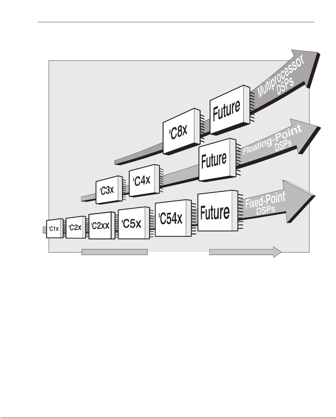
Figure 1–1. TMS320 Family
TMS320 Family
Performance
Introduction
1-3
Page 29

TMS320 Family
1.1.2 Typical Applications for the TMS320 Family
T able 1–1 lists some typical applications for the TMS320 family of DSPs. The
TMS320 DSPs offer adaptable approaches to traditional signal-processing
problems such as filtering and vocoding. They also support complex
applications that often require multiple operations to be performed simultaneously.
Table 1–1. Typical Applications for TMS320 DSPs
Automotive Consumer Control
Adaptive ride control
Antiskid brakes
Cellular telephones
Digital radios
Engine control
Global positioning
Navigation
Vibration analysis
Voice commands
General-Purpose Graphics/Imaging Industrial
Adaptive filtering
Convolution
Correlation
Digital filtering
Fast Fourier transforms
Hilbert transforms
Waveform generation
Windowing
Instrumentation Medical Military
Digital filtering
Function generation
Pattern matching
Phase-locked loops
Seismic processing
Spectrum analysis
Transient analysis
Digital radios/TVs
Educational toys
Music synthesizers
Pagers
Power tools
Radar detectors
Solid-state answering machines
3-D rotation
Animation/digital maps
Homomorphic processing
Image compression/transmission
Image enhancement
Pattern recognition
Robot vision
Workstations
Diagnostic equipment
Fetal monitoring
Hearing aids
Patient monitoring
Prosthetics
Ultrasound equipment
Disk drive control
Engine control
Laser printer control
Motor control
Robotics control
Servo control
Numeric control
Power-line monitoring
Robotics
Security access
Image processing
Missile guidance
Navigation
Radar processing
Radio frequency modems
Secure communications
Sonar processing
Telecommunications Voice/Speech
1200- to 28 800-bps modems
Adaptive equalizers
ADPCM transcoders
Cellular telephones
Channel multiplexing
Data encryption
Digital PBXs
Digital speech interpolation (DSI)
DTMF encoding/decoding
Echo cancellation
1-4
Faxing
Line repeaters
Personal communications
systems (PCS)
Personal digital assistants (PDA)
Speaker phones
Spread spectrum communications
Video conferencing
X.25 packet switching
Speaker verification
Speech enhancement
Speech recognition
Speech synthesis
Speech vocoding
Text-to-speech applications
Voice mail
Page 30

1.2 TMS320C2xx Generation
T exas Instruments uses static CMOS integrated-circuit technology to fabricate
the TMS320C2xx DSPs. The architectural design of the ’C2xx is based on that
of the ’C5x. The operational flexibility and speed of the ’C2xx and ’C5x are a
result of an advanced, modified Harvard architecture (which has separate
buses for program and data memory), a multilevel pipeline, on-chip peripherals, on-chip memory , and a highly specialized instruction set. The ’C2xx performs up to 40 MIPS (million instructions per second).
The ’C2xx generation offers the following benefits:
-
Enhanced TMS320 architectural design for increased performance and
versatility
-
Modular architectural design for fast development of additional spin-off
devices
-
Advanced IC processing technology for increased performance
-
Fast and easy performance upgrades for ’C1x and ’C2x source code,
which is upward compatible with ’C2xx source code
TMS320C2xx Generation
-
Enhanced instruction set for faster algorithms and for optimized high-level
language operation
-
New static design techniques for minimizing power consumption
Table 1–2 provides an overview of the basic features of the ’C2xx DSPs.
Table 1–2. ’C2xx Generation Summary
On-Chip Memory Serial Ports
Cycle Time
Device
TMS320C203
TMS320C204 25/35/50 544 4K 1 1 1 100 TQFP
TMS320F206 25/35/50 4.5K 32K 1 1 1 100 TQFP
TMS320C209 35/50 4.5K 4K – – 1 80 TQFP
†
TQFP = Thin quad flat pack
(ns)
25/35/50 544 1 1 1 100 TQFP
RAM ROM Flash Synch. Asynch. Timers Package
†
†
†
†
Introduction
1-5
Page 31

Key Features of the TMS320C2xx
1.3 Key Features of the TMS320C2xx
Key features on the various ’C2xx devices are:
-
Speed:
J
50-, 35-, or 25-ns execution time of a single-cycle instruction
J
20, 28.5, or 40 MIPS
-
Code compatibility with other TMS320 fixed-point devices:
J
Source-code compatible with all ’C1x and ’C2x devices
J
Upward compatible with the ’C5x devices
-
Memory:
J
224K words of addressable memory space (64K words of program
space, 64K words of data space, 64K words of I/O space, and 32K
words of global space)
J
544 words of dual-access on-chip RAM (288 words for data and 256
words for program/data)
J
4K words on-chip ROM or 32K words on-chip flash memory (on
selected devices)
J
4K words of single-access on-chip RAM (on selected devices)
-
CPU:
J
32-bit arithmetic logic unit (CALU)
J
32-bit accumulator
J
16-bit × 16-bit parallel multiplier with 32-bit product capability
J
Three scaling shifters
J
Eight 16-bit auxiliary registers with a dedicated arithmetic unit for indirect addressing of data memory
-
Program control:
J
4-level pipeline operation
J
8-level hardware stack
J
User-maskable interrupt lines
1-6
Page 32

-
Instruction set:
J
Single-instruction repeat operation
J
Single-cycle multiply/accumulate instructions
J
Memory block move instructions for better program/data
management
J
Indexed-addressing capability
J
Bit-reversed indexed-addressing capability for radix-2 FFTs
-
On-chip peripherals:
J
Software-programmable timer
J
Software-programmable wait-state generator for program, data, and
I/O memory spaces
J
Oscillator and phase-locked loop (PLL) to implement clock options:
×1, ×2, ×4, and
J
CLK register for turning the CLKOUT1 pin on and off (not available on
’C209)
Key Features of the TMS320C2xx
÷2 (only ×2 and ÷2 available on ’C209)
J
Synchronous serial port (not available on ’C209)
J
Asynchronous serial port (not available on ’C209)
-
On-chip scanning-logic circuitry (IEEE Standard 1149.1) for emulation
and testing purposes
-
Power:
J
5- or 3.3-V static CMOS technology
J
Power-down mode to reduce power consumption
-
Packages:
J
100-pin TQFP (thin quad flat pack)
J
80-pin TQFP for the ’C209
Introduction
1-7
Page 33

Chapter 2
Architectural Overview
This chapter provides an overview of the architectural structure and components of the ’C2xx. The ’C2xx DSPs use an advanced, modified Harvard architecture that maximizes processing power by maintaining separate bus structures for program memory and data memory . The three main components of
the ’C2xx are the central processing unit (CPU), memory , and on-chip peripherals.
Figure 2–1 shows an overall block diagram of the ’C2xx.
Note:
All ’C2xx devices use the same central processing unit (CPU), bus structure,
and instruction set, but the ’C209 has some notable differences. For example, although certain peripheral control registers have the same names on
all ’C2xx devices, these registers are located at different I/O addresses on
the ’C209. See Chapter 1 1 for a detailed description of the differences on the
’C209.
T opic Page
2.1 ’C2xx Bus Structure 2-3. . . . . . . . . . . . . . . . . . . . . . . . . . . . . . . . . . . . . . . . . . .
2.2 Central Processing Unit 2-5. . . . . . . . . . . . . . . . . . . . . . . . . . . . . . . . . . . . . . .
2.3 Memory and I/O Spaces 2-7. . . . . . . . . . . . . . . . . . . . . . . . . . . . . . . . . . . . . . .
2.4 Program Control 2-10. . . . . . . . . . . . . . . . . . . . . . . . . . . . . . . . . . . . . . . . . . . . .
2.5 On-Chip Peripherals 2-11. . . . . . . . . . . . . . . . . . . . . . . . . . . . . . . . . . . . . . . . . .
2.6 Scanning-Logic Circuitry 2-13. . . . . . . . . . . . . . . . . . . . . . . . . . . . . . . . . . . . .
Architectural Overview
2-1
Page 34

Architectural Overview
Figure 2–1. Overall Block Diagram of the ’C2xx
PRDB
DRDB
MUX
NPAR
MUX
PAB
ROM/flash
SARAM
DARAM
B0
DARAM
B1, B2
ST0
ST1
IMR
IFR
GREG
PC
MUX
Input shifter
Output shifter
DWEB
PAB
TREG
MUX
CALU
Accumulator
DWEB
MSTACKPAR
Multiplier
16 × 16
PREG
Product shifter
Stack 8 × 16
MUX
Auxiliary
registers
8 × 16
Program
control
AR0
MUX
ARAU
MUXMUX
DWAB
DRAB
PRDB
Note: The I/O-mapped (peripheral) registers are not part of the core; they are accessed as shown in Figure 2–2 on page 2-4.
2-2
DWAB
DRAB
DRDB
Page 35

2.1 ’C2xx Bus Structure
Figure 2–2 shows a block diagram of the ’C2xx bus structure. The ’C2xx internal architecture is built around six 16-bit buses:
-
PAB. The
and writes to program memory.
-
DRAB. The
data memory.
-
DWAB. The
memory .
-
PRDB. The
operands, as well as table information, from program memory to the CPU.
-
DRDB. The
arithmetic logic unit (CALU) and the auxiliary register arithmetic unit
(ARAU).
-
DWEB. The
memory .
program address bus
data-read address bus
data-write address bus
program read bus
data read bus
data write bus
carries data from data memory to the central
carries data to both program memory and data
’C2xx Bus Structure
provides addresses for both reads from
provides addresses for reads from
provides addresses for writes to data
carries instruction code and immediate
Having separate address buses for data reads (DRAB) and data writes
(DWAB) allows the CPU to read and write in the same machine cycle.
Separate program and data spaces allow simultaneous access to program
instructions and data. For example, while data is multiplied, a previous product
can be added to the accumulator, and, at the same time, a new address can
be generated. Such parallelism supports a set of arithmetic, logic, and bit-manipulation operations that can all be performed in a single machine cycle. In
addition, the ’C2xx includes control mechanisms to manage interrupts, repeated operations, and function/subroutine calls.
All ’C2xx devices share the same CPU and bus structure; however, each device has different on-chip memory configurations and on-chip peripherals.
Architectural Overview
2-3
Page 36

’C2xx Bus Structure
Figure 2–2. Bus Structure Block Diagram
External
address bus
External
data bus
On-chip peripherals/
registers mapped to
I/O space
Timer
Wait-state
generator
Synchronous
serial port
UART
Other I/O-mapped
registers
ROM/
flash
SARAM
PAB
DRAB
DWAB
PRDB
DRDB
DWEB
Central processing unit (CPU)
ARAU
Auxiliary
registers
Status
registers
Input
shifter
CALU
Accumulator
Output
shifter
B0
DARAM
Multiplier
TREG
PREG
Product
shifter
B1, B2
DARAM
Memory
mapped
registers
Control bus
External
signals
Memory
control
MULTI_DSP
CLOCK/PLL
Interrupts
JTAG/TEST
2-4
Page 37

2.2 Central Processing Unit
The CPU is the same on all the ’C2xx devices. The ’C2xx CPU contains:
-
A 32-bit central arithmetic logic unit (CALU)
-
A 32-bit accumulator
-
Input and output data-scaling shifters for the CALU
-
A 16-bit × 16-bit multiplier
-
A product-scaling shifter
-
Data-address generation logic, which includes eight auxiliary registers
and an auxiliary register arithmetic unit (ARAU)
-
Program-address generation logic
2.2.1 Central Arithmetic Logic Unit (CALU) and Accumulator
The ’C2xx performs 2s-complement arithmetic using the 32-bit CALU. The
CALU uses 16-bit words taken from data memory or derived from an immediate instruction, or it uses the 32-bit result from the multiplier. In addition to arithmetic operations, the CALU can perform Boolean operations.
The accumulator stores the output from the CALU; it can also provide a second
input to the CALU. The accumulator is 32 bits wide and is divided into a highorder word (bits 31 through 16) and a low-order word (bits 15 through 0).
Assembly language instructions are provided for storing the high- and loworder accumulator words to data memory.
Central Processing Unit
2.2.2 Scaling Shifters
The ’C2xx has three 32-bit shifters that allow for scaling, bit extraction, extended arithmetic, and overflow-prevention operations:
-
-
-
Input data-scaling shifter (input shifter). This shifter left shifts 16-bit input data by 0 to 16 bits to align the data to the 32-bit input of the CALU.
Output data-scaling shifter (output shifter). This shifter can left shift
output from the accumulator by 0 to 7 bits before the output is stored to
data memory. The content of the accumulator remains unchanged.
Product-scaling shifter (product shifter). The product register (PREG)
receives the output of the multiplier. The product shifter shifts the output
of the PREG before that output is sent to the input of the CALU. The product shifter has four product shift modes (no shift, left shift by one bit, left
shift by four bits, and right shift by 6 bits), which are useful for performing
multiply/accumulate operations, performing fractional arithmetic, or justifying fractional products.
Architectural Overview
2-5
Page 38

Central Processing Unit
2.2.3 Multiplier
The on-chip multiplier performs 16-bit × 16-bit 2s-complement multiplication
with a 32-bit result. In conjunction with the multiplier, the ’C2xx uses the 16-bit
temporary register (TREG) and the 32-bit product register (PREG). The TREG
always supplies one of the values to be multiplied. The PREG receives the result of each multiplication.
Using the multiplier, TREG, and PREG, the ’C2xx ef ficiently performs fundamental DSP operations such as convolution, correlation, and filtering. The effective execution time of each multiplication instruction can be as short as one
CPU cycle.
2.2.4 Auxiliary Register Arithmetic Unit (ARAU) and Auxiliary Registers
The ARAU generates data memory addresses when an instruction uses indirect addressing (see Chapter 6,
The ARAU is supported by eight auxiliary registers (AR0 through AR7), each
of which can be loaded with a 16-bit value from data memory or directly from
an instruction word. Each auxiliary register value can also be stored to data
memory. The auxiliary registers are referenced by a 3-bit auxiliary register
pointer (ARP) embedded in status register ST0.
Addressing Modes
) to access data memory .
2-6
Page 39

2.3 Memory and I/O Spaces
The ’C2xx memory is organized into four individually selectable spaces: program, local data, global data, and I/O. These spaces form an address range
of 224K words.
All ’C2xx devices include 288 words of dual-access RAM (DARAM) for data
memory and 256 words of data/program DARAM. Depending on the device,
it may also have data/program single-access RAM (SARAM) and read-only
memory (ROM) or flash memory. Table 2–1 shows how much ROM, flash
memory, DARAM, and SARAM are available on the different ’C2xx devices.
Table 2–1. Program and Data Memory on the TMS320C2xx Devices
Memory T ype ’C203 ’C204 ’F206 ’C209
ROM (words) – 4K – 4K
Flash memory (words) – – 32K –
DARAM (words) 544 544 544 544
Memory and I/O Spaces
Data (words)
Data/program (words)
SARAM (words)
The ’C2xx also has CPU registers that are mapped in data memory space and
peripheral registers that are mapped in on-chip I/O space. The ’C2xx memory
types and features are introduced in the subsections following this paragraph.
For more details about the configuration and use of the ’C2xx memory and I/O
space, see Chapter 4,
2.3.1 Dual-Access On-Chip RAM
All ’C2xx devices have 544 words × 16-bits of on-chip DARAM, which can be
accessed twice per machine cycle. This memory is primarily intended to hold
data but, when needed, can also hold programs. It can be configured in one
of two ways:
-
All 544 words are configured as data memory.
-
288 words are configured as data memory , and 256 words are configured
as program memory.
Because DARAM can be accessed twice per cycle, it improves the speed of
the CPU. The CPU operates within a four-cycle pipeline. In this pipeline, the
288 288 288 288
256 256 256 256
– – 4K 4K
Memory and I/O Space
.
Architectural Overview
2-7
Page 40

Memory and I/O Spaces
CPU reads data on the third cycle and writes data on the fourth cycle. However,
DARAM allows the CPU to write and read in one cycle; the CPU writes to
DARAM on the master phase of the cycle and reads from DARAM on the slave
phase. For example, suppose two instructions, A and B, store the accumulator
value to DARAM and load the accumulator with a new value from DARAM.
Instruction A stores the accumulator value during the master phase of the CPU
cycle, and instruction B loads the new value to the accumulator during the
slave phase. Because part of the dual-access operation is a write, it only applies to RAM.
2.3.2 Single-Access On-Chip Program/Data RAM
Some of the ’C2xx devices have 4K 16-bit words of single-access RAM
(SARAM). The addresses associated with the SARAM can be used for both
data memory and program memory and are software- or hardware-configurable (depending on the device) to either external memory or the internal
SARAM. When configured as external, these addresses can be used for offchip data and program memory . Code can be booted from of f-chip ROM and
then executed at full speed once it is loaded into the on-chip SARAM. Because
the SARAM can be mapped to program and/or data memory , the SARAM allows for more flexible address mapping than the DARAM block.
SARAM is accessed only once per CPU cycle. When the CPU requests multiple accesses, the SARAM schedules the accesses by providing a not-ready
condition to the CPU and then executing the accesses one per cycle. For example, if the instruction sequence involves storing the accumulator value and
then loading a value to the accumulator, it would take two cycles to complete
in SARAM, compared to one cycle in DARAM.
2.3.3 Factory-Masked On-Chip ROM
Some of the ’C2xx devices feature an on-chip, 4K 16-bit words of programmable ROM. The ROM can be selected during reset by driving the MP/MC
low. If the ROM is not selected, the device starts its execution from off-chip
memory.
If you want a custom ROM, you can provide the code or data to be programmed into the ROM in object file format, and T exas Instruments will generate the appropriate process mask to program the ROM. See Appendix D for
details on how to submit ROM code to Texas Instruments.
2-8
pin
Page 41

2.3.4 Flash Memory
Memory and I/O Spaces
Some of the ’C2xx devices feature on-chip blocks of flash memory, which is
electronically erasable and programmable, and non-volatile. Each block of
flash memory will have a set of control registers that allow for erasing, programming, and testing of that block. The flash memory blocks can be selected
during reset by driving the MP/MC
pin low. If the flash memory is not selected,
the device starts its execution from off-chip memory.
Architectural Overview
2-9
Page 42

Program Control
Program Control
2.4 Program Control
Several features provide program control:
-
-
The program controller of the CPU decodes instructions, manages the
pipeline, stores the status of operations, and decodes conditional operations. Elements involved in program control are the program counter, the
status registers, the stack, and the address-generation logic.
Software mechanisms used for program control include branches, calls,
conditional instructions, a repeat instruction, reset, and interrupts.
For descriptions of these program control features, see Chapter 5,
Control.
Program
2-10
Page 43

2.5 On-Chip Peripherals
All the ’C2xx devices have the same CPU, but different on-chip peripherals are
connected to their CPUs. The on-chip peripherals featured on the ’C2xx devices are:
-
Clock generator (an oscillator and a phase lock loop circuit)
-
CLK register for turning the CLKOUT1 pin on and off
-
Timer
-
Wait-state generator
-
General-purpose input/output (I/O) pins
-
Synchronous serial port
-
Asynchronous serial port
2.5.1 Clock Generator
The clock generator consists of an internal oscillator and an internal phase lock
loop (PLL) circuit. The clock generator can be driven internally by connecting
the DSP to a crystal resonator circuit, or it can be driven by an external clock
source. The PLL circuit generates an internal CPU clock by multiplying the
clock source by a specified factor. Thus, you can use a clock source with a lower frequency than that of the CPU. The clock generator is discussed in Section
8.2, on page 8-4.
On-Chip Peripherals
2.5.2 CLKOUT1-Pin Control (CLK) Register
The ’C2xx CLK register controls whether the master clock output signal
(CLKOUT1) is available at the CLKOUT1 pin.
2.5.3 Hardware Timer
The ’C2xx features a 16-bit down-counting timer with a 4-bit prescaler. Timer
control bits can stop, start, reload, and determine the prescaler count for the
timer. For more information, see Section 8.4,
2.5.4 Software-Programmable Wait-State Generator
Software-programmable wait-state logic is incorporated (without any external
hardware) for interfacing with slower off-chip memory and I/O devices. The
’C209 wait-state generator generates zero or one wait states; the wait-state
generator on other ’C2xx devices generates zero to seven wait states. For
more information, see Section 8.5,
Wait-State Generator
Timer
, on page 8-8.
, on page 8-14.
Architectural Overview
2-1 1
Page 44

On-Chip Peripherals
2.5.5 General-Purpose I/O Pins
The ’C2xx has pins that provide general-purpose input or output signals. All
’C2xx devices have a general-purpose input pin, BIO
output pin, XF . Except for the ’C209, the ’C2xx devices also have pins IO0, IO1,
IO2, and IO3, which are connected to corresponding bits (IO0–IO3) mapped
into the on-chip I/O space. These bits can be individually configured as inputs
or outputs. For more information on the general-purpose pins, see Section 8.6,
on page 8-17.
2.5.6 Serial Ports
The serial ports available on the ’C2xx vary by device, but two types of serial
ports are represented: synchronous and asynchronous. See T able 2–2 for the
number of each kind on the various ’C2xx devices. The subsections following
the table provide an introduction to the two types of serial ports.
Table 2–2. Serial Ports on the ’C2xx Devices
Serial Ports ’C203 ’C204 ’F206 ’C209
Synchronous 1 1 1 –
Asynchronous 1 1 1 –
, and a general-purpose
Synchronous serial port (SSP)
The ’C2xx synchronous serial port (SSP) communicates with codecs, other
’C2xx devices, and external peripherals. The SSP offers:
-
Two four-word-deep first in, first out (FIFO) buf fers that have interrupt-generating capabilities.
-
Burst and continuous transfer modes.
-
A wide range of operation speeds when external clocking is used.
If internal clocking is used, the speed is fixed at 1/2 of the internal DSP clock
frequency. For more information on the SSP, see Chapter 9.
Asynchronous serial port (ASP)
The ’C2xx asynchronous serial port (ASP) communicates with asynchronous
serial devices. The ASP has a maximum transfer rate of 250,000 characters
per second (assuming it uses10 bits to transmit each 8-bit character). The ASP
also has logic for automatic baud detection, which allows the ASP to lock to
the incoming data rate. All transfers through the asynchronous serial port use
double buffering. See Chapter 10,
formation.
2-12
Asynchronous Serial Port,
for more in-
Page 45

2.6 Scanning-Logic Circuitry
The ’C2xx has JTAG scanning-logic circuitry that is compatible with IEEE
Standard 1149.1. This circuitry is used for emulation and testing purposes
only . The serial scan path is used to test pin-to-pin continuity as well as to perform operational tests on the on-chip peripherals. The internal scanning logic
provides access to all of the on-chip resources. Thus, the serial-scan pins and
the emulation pins on ’C2xx devices allow on-board emulation. However, on
all ’C2xx devices, the serial scan path does not have boundary scan logic.
Appendix E provides information to help you meet the design requirements of
the Texas Instruments XDS510 emulator with respect to IEEE-1149.1 designs and discusses the XDS510 cable.
Scanning-Logic Circuitry
Scanning-Logic Circuitry
Architectural Overview
2-13
Page 46

Chapter 3
Central Processing Unit
This chapter describes the main components of the central processing unit
(CPU). First, this chapter describes three fundamental sections of the CPU
(see Figure 3–1):
-
Input scaling section
-
Multiplication section
-
Central arithmetic logic section
The chapter then describes the auxiliary register arithmetic unit (ARAU), which
performs arithmetic operations independently of the central arithmetic logic
section. The chapter concludes with a description of status registers ST0 and
ST1, which contain bits for determining processor modes, addressing pointer
values, and indicating various processor conditions and arithmetic logic results.
Topic Page
3.1 Input Scaling Section 3-3. . . . . . . . . . . . . . . . . . . . . . . . . . . . . . . . . . . . . . . . . .
3.2 Multiplication Section 3-5. . . . . . . . . . . . . . . . . . . . . . . . . . . . . . . . . . . . . . . . .
3.3 Central Arithmetic Logic Section 3-8. . . . . . . . . . . . . . . . . . . . . . . . . . . . . . .
3.4 Auxiliary Register Arithmetic Unit (ARAU) 3-12. . . . . . . . . . . . . . . . . . . . .
3.5 Status Registers ST0 and ST1 3-15. . . . . . . . . . . . . . . . . . . . . . . . . . . . . . . . .
3-1
Page 47

Central Processing Unit
Figure 3–1. Block Diagram of the Input Scaling, Central Arithmetic Logic, and
Multiplication Sections of the CPU
Data write bus (DWEB)
Data read bus (DRDB)
Program read bus (PRDB)
Input scaling
section
31
Input shifter (32 bits)
32
Central arithmetic logic
section
32
16
16
MUX MUX
16
016 15
C
16
Multiplication
section
CALU
1
1
Accumulator
Output shifter (32 bits)
Product shifter (32 bits)
MUX
32
32
16
TREG
Multiplier
16 × 16
PREG
32
32
32
16
16
1
1
16
16
16
3-2
Page 48

3.1 Input Scaling Section
A 32-bit input data-scaling shifter (input shifter) aligns a 16-bit value coming
from memory to the 32-bit CALU. This data alignment is necessary for datascaling arithmetic as well as aligning masks for logical operations. The input
shifter operates as part of the data path between program or data space and
the CALU and, thus, requires no cycle overhead. Described directly below are
the input, the output, and the shift count of the input shifter. Throughout the discussion, refer to Figure 3–2.
Figure 3–2. Block Diagram of the Input Scaling Section
From program memory (PRDB)
From data memory (DRDB)
16
16
Input scaling section
MUX
16
Input Scaling Section
31
Input shifter (32 bits)
32
To CALU
016 15
Input. Bits 15 through 0 of the input shifter accept a 16-bit input from either of
two sources (see Figure 3–2):
-
The data read bus (DRDB).
This input is a value from a data memory loca-
tion referenced in an instruction operand.
-
The program read bus (PRDB).
This input is a constant value given as an
instruction operand.
Output. After a value has been accepted into bits 15 through 0, the input shifter
aligns the16-bit value to the 32-bit bus of the CALU as shown in Figure 3–2.
The shifter shifts the value left 0 to 16 bits and then sends the 32-bit result to
the CALU.
During the left shift, unused LSBs in the shifter are filled with zeros, and unused
MSBs in the shifter are either filled with zeros or sign extended, depending on
the value of the sign-extension mode bit (SXM) of status register ST1.
Central Processing Unit
3-3
Page 49

Input Scaling Section
Shift count. The shifter can left-shift a 16-bit value by 0 to 16 bits. The size
of the shift (or the shift count) is obtained from one of two sources:
-
A constant embedded in the instruction word.
Putting the shift count in the
instruction word allows you to use specific data-scaling or alignment operations customized for your program code.
-
The four LSBs of the temporary register (TREG).
The TREG-based shift
allows the data-scaling factor to be determined dynamically so that it can
be adapted to the system’s performance.
Sign-extension mode bit. For many but not all instructions, the sign-extension mode bit (SXM), bit 10 of status register ST1, determines whether the
CALU uses sign extension during its calculations. If SXM = 0, sign extension
is suppressed. If SXM = 1, the output of the input shifter is sign extended.
Figure 3–3 shows an example of an input value shifted left by 8 bits for
SXM = 0. The MSBs of the value passed to the CALU are zero filled.
Figure 3–4 shows the same shift but with SXM = 1. The value is sign extended
during the shift.
Figure 3–3. Operation of the Input Shifter for SXM = 0
Input shifter
accepting the
value
Output value
after left shift of 8
(SXM = 0)
Figure 3–4. Operation of the Input Shifter for SXM = 1
Input shifter
accepting the
value
Output value
after left shift of 8
(SXM = 1)
A F 1 1
16
X X X X A F 1 1
32
0 0 A F 1 1 0 0
A F 1 1
16
X X X X A F 1 1
32
F F A F 1 1 0 0
3-4
Page 50

3.2 Multiplication Section
The ’C2xx uses a 16-bit × 16-bit hardware multiplier that can produce a signed
or unsigned 32-bit product in a single machine cycle. As shown in Figure 3–5,
the multiplication section consists of:
-
The 16-bit temporary register (TREG), which holds one of the multiplicands
-
The multiplier, which multiplies the TREG value by a second value from
data memory or program memory
-
The 32-bit product register (PREG), which receives the result of the multiplication
-
The product shifter, which scales the PREG value before passing it to the
CALU.
Figure 3–5. Block Diagram of the Multiplication Section
From data memory
Multiplication Section
From data memory
From program memory
3.2.1 Multiplier
16
16
MUX
16
To data memory
From data
memory
16
To high word
of PREG
Multiplication
section
Product shifter (32 bits)
16
TREG
Multiplier
16 × 16
PREG
32
32
To CALU
16
The 16-bit × 16-bit hardware multiplier can produce a signed or unsigned
32-bit product in a single machine cycle. The two numbers being multiplied are
treated as 2s-complement numbers, except during unsigned multiplication
(MPYU instruction). Descriptions of the inputs and output of the multiplier follow.
Central Processing Unit
3-5
Page 51

Multiplication Section
Inputs. The multiplier accepts two 16-bit inputs:
-
One input is always from the 16-bit temporary register (TREG). The TREG
is loaded before the multiplication with a data-value from the data read bus
(DRDB).
-
The other input is one of the following:
J
A data-memory value from the data read bus (DRDB).
J
A program memory value from the program read bus (PRDB).
Output. After the two 16-bit inputs are multiplied, the 32-bit result is stored in
the product register (PREG). The output of the PREG is connected to the 32-bit
product-scaling shifter. Through this shifter, the product may be transferred
from the PREG to the CALU or to data memory (by the SPH and SPL instructions).
3.2.2 Product-Scaling Shifter
The product-scaling shifter (product shifter) facilitates scaling of the product
register (PREG) value. The shifter has a 32-bit input connected to the output
of the PREG and a 32-bit output connected to the input of the CALU.
3-6
Input. The shifter has a 32-bit input connected to the output of the PREG.
Output. After the shifter completes the shift, all 32 bits of the result can be
passed to the CALU, or 16 bits of the result can be stored to data memory.
Shift Modes. This shifter uses one of four product shift modes, summarized
in T able 3–1. As shown in the table, these modes are determined by the product shift mode (PM) bits of status register ST1. In the first shift mode (PM = 00),
the shifter does not shift the product at all before giving it to the CALU or to data
memory . The next two modes cause left shifts (of one or four), which are useful
for implementing fractional arithmetic or justifying products. The right-shift
mode shifts the product by six bits, enabling the execution of up to 128 consecutive multiply-and-accumulate operations without causing the accumulator to
overflow. Note that the content of the PREG remains unchanged; the value is
copied to the product shifter and shifted there.
Note:
The right shift in the product shifter is always sign extended, regardless of
the value of the sign-extension mode bit (SXM) of status register ST1.
Page 52

Table 3–1. Product Shift Modes for the Product-Scaling Shifter
Á
Á
Á
Á
Á
Á
Á
Á
Á
Á
Á
PM
Shift
00
no shift
01
left 1
ÁÁ
10
left 4
ÁÁ
ÁÁ
11
right 6
ÁÁ
ÁÁ
†
A Q31 number is a binary fraction in which there are 31 digits to the right of the binary point
БББББББББББББББББББББ
(the base 2 equivalent of the base 10 decimal point).
Comments
Product sent to CALU or data write bus (DWEB) with no shift
Removes the extra sign bit generated in a 2s-complement multiply
БББББББББББББББББ
to produce a Q31 product
Removes the extra four sign bits generated in a 16-bit × 13-bit 2s-
БББББББББББББББББ
complement multiply to produce a Q31 product† when multiplying
by a 13-bit constant
БББББББББББББББББ
†
Scales the product to allow up to 128 product accumulations without overflowing the accumulator . The right shift is always sign ex-
БББББББББББББББББ
tended, regardless of the value of the sign-extension mode bit
БББББББББББББББББ
(SXM) of status register ST1.
Multiplication Section
Central Processing Unit
3-7
Page 53

Central Arithmetic Logic Section
3.3 Central Arithmetic Logic Section
Figure 3–6 shows the main components of the central arithmetic logic section,
which are:
-
The central arithmetic logic unit (CALU), which implements a wide range
of arithmetic and logic functions.
-
The 32-bit accumulator (ACC), which receives the output of the CALU and
is capable of performing bit shifts on its contents with the help of the carry
bit (C). Figure 3–6 shows the accumulator’s high word (ACCH) and low
word (ACCL).
-
The output shifter, which can shift a copy of either the high word or low
word of the accumulator before sending it to data memory for storage.
Figure 3–6. Block Diagram of the Central Arithmetic Logic Section
From input shifter
From product shifter
3232
Central arithmetic logic
section
32
C
MUX
32
CALU
32
ACCH
Output shifter (32 bits)
To data memory
ACCL
32
16
3-8
Page 54

3.3.1 Central Arithmetic Logic Unit (CALU)
The central arithmetic logic unit (CALU), implements a wide range of arithmetic and logic functions, most of which execute in a single clock cycle. These
functions can be grouped into four categories:
-
16-bit addition
-
16-bit subtraction
-
Boolean logic operations
-
Bit testing, shifting, and rotating.
Because the CALU can perform Boolean operations, you can perform bit manipulation. For bit shifting and rotating, the CALU uses the accumulator. The
CALU is referred to as central because there is an independent arithmetic unit,
the auxiliary register arithmetic unit (ARAU), which is described in Section 3.4.
A description of the inputs, the output, and an associated status bit of the CALU
follows.
Inputs. The CALU has two inputs (see again Figure 3–6):
-
One input is always provided by the 32-bit accumulator.
Central Arithmetic Logic Section
3.3.2 Accumulator
-
The other input is provided by one of the following:
J
The product-scaling shifter (see subsection 3.2.2)
J
The input data-scaling shifter (see Section 3.1)
Output. Once the CALU performs an operation, it transfers the result to the
32-bit accumulator, which is capable of performing bit shifts of its contents. The
output of the accumulator is connected to the 32-bit output data-scaling shifter.
Through the output shifter, the accumulator’s upper and lower 16-bit words
can be individually shifted and stored to data memory.
Sign-extension mode bit. For many but not all instructions, the sign-extension mode bit (SXM), bit 10 of status register ST1, determines whether the
CALU uses sign extension during its calculations. If SXM = 0, sign extension
is suppressed. If SXM = 1, sign extension is enabled.
Once the CALU performs an operation, it transfers the result to the 32-bit accumulator, which can then perform single-bit shifts or rotations on its contents.
Each of the accumulator’s upper and lower 16-bit words can be passed to the
output data-scaling shifter, where it can be shifted, and then stored in data
memory . Status bits and branch instructions associated with the accumulator
are discussed directly below.
Central Processing Unit
3-9
Page 55

Central Arithmetic Logic Section
Status bits. Four status bits are associated with the accumulator:
-
Carry bit (C).
J
Additions to and subtractions from the accumulator:
C (bit 9 of status register ST1) is affected during:
C = 0 When the result of a subtraction generates a borrow.
When the result of an addition does not generate a carry . (Exception: When the ADD instruction is used with a shift of 16 and
no carry is generated, the ADD instruction has no affect on C.)
C = 1 When the result of an addition generates a carry.
When the result of a subtraction does not generate a borrow.
(Exception: When the SUB instruction is used with a shift of 16
and no borrow is generated, the SUB instruction has no effect
on C.)
J
Single-bit shifts and rotations of the accumulator value. During a left
shift or rotation, the most significant bit of the accumulator is passed to
C; during a right shift or rotation, the least significant bit is passed to C.
-
Overflow mode bit (OVM).
OVM (bit 1 1 of status register ST0) determines
how the accumulator will reflect arithmetic overflows. When the processor
is in overflow mode (OVM = 1) and an overflow occurs, the accumulator
is filled with one of two specific values:
J
If the overflow is in the positive direction, the accumulator is filled with
its most positive value (7FFF FFFFh).
J
If the overflow is in the negative direction, the accumulator is filled with
its most negative value (8000 0000h).
-
Overflow flag bit (OV).
OV is bit 12 of status register ST0. When no accumulator overflow is detected, OV is latched at 0. When overflow (positive
or negative) occurs, OV is set to 1 and latched.
-
T est/control flag bit (TC).
TC (bit 1 1 of status register ST1) is set to 0 or 1
depending on the value of a tested bit. In the case of the NORM instruction,
if the exclusive-OR of the two MSBs of the accumulator is true, TC is set
to 1.
A number of branch instructions are implemented based on the status of bits
C, OV , and TC, and on the value in the accumulator (as compared to zero). For
more information about these instructions, see Section 5.4,
Branches, Calls, and Returns
, on page 5-10.
Conditional
3-10
Page 56

Central Arithmetic Logic Section
3.3.3 Output Data-Scaling Shifter
The output data-scaling shifter (output shifter) has a 32-bit input connected to
the 32-bit output of the accumulator and a 16-bit output connected to the data
bus. The shifter copies all 32-bits of the accumulator and then performs a left
shift on its content; it can be shifted from zero to seven bits, as specified in the
corresponding store instruction. The upper word (SACH instruction) or lower
word (SACL instruction) of the shifter is then stored to data memory . The content of the accumulator remains unchanged.
When the output shifter performs the shift, the MSBs are lost and the LSBs are
zero filled. Figure 3–7 shows an example in which the accumulator value is
shifted left by four bits and the shifted high word is stored to data memory.
Figure 3–8 shows the same accumulator value shifted left by 6 bits and then
the shifted low word stored.
Figure 3–7. Shifting and Storing the High Word of the Accumulator
Accumulator
Output shifter
(left shift by 4 bits)
Data-memory
location
0 0 F 0
0 F 0 F
16
0 F 0 F
F 0 A 1
32
0 A 1 0
Figure 3–8. Shifting and Storing the Low Word of the Accumulator
Accumulator
Output shifter
(left shift by 6 bits)
0 0 F 0
3 C 3 C
Data-memory
location
F 0 A 1
32
2 8 4 0
16
2 8 4 0
Central Processing Unit
3-1 1
Page 57

Auxiliary Register Arithmetic Unit (ARAU)
3.4 Auxiliary Register Arithmetic Unit (ARAU)
The CPU also contains the auxiliary register arithmetic unit (ARAU), an arithmetic unit independent of the central arithmetic logic unit (CALU). The main
function of the ARAU is to perform arithmetic operations on eight auxiliary registers (AR7 through AR0) in parallel with operations occurring in the CALU.
Figure 3–9 shows the ARAU and related logic.
Figure 3–9.ARAU and Related Logic
Data read bus (DRDB)
ARB
16
16
16
16
16
16
16
16
16
16
ARAU
16
16
AR7
AR6
AR5
AR4
AR3
AR2
AR1
AR0
MUX
3
ARP
3
MUX
3
3LSBs
Instruction register
8LSBs
Data write bus (DWEB)
3-12
Data-read address bus (DRAB)
Data-write address bus (DWAB)
Page 58

Auxiliary Register Arithmetic Unit (ARAU)
The eight auxiliary registers (AR7–AR0) provide flexible and powerful indirect
addressing. Any location in the 64K data memory space can be accessed using a 16-bit address contained in an auxiliary register. For the details of indirect
addressing, see Section 6.3 on page 6-9.
To select a specific auxiliary register, load the 3-bit auxiliary register pointer
(ARP) of status register ST0 with a value from 0 through 7. The ARP can be
loaded as a primary operation by the MAR instruction (which only performs
modifications to the auxiliary registers and the ARP) or by the LST instruction
(which can load a data-memory value to ST0 by way of the data read bus,
DRDB). The ARP can be loaded as a secondary operation by any instruction
that supports indirect addressing.
The register pointed to by the ARP is referred to as the
or
current AR
. During the processing of an instruction, the content of the current auxiliary register is used as the address at which the data-memory access
will take place. The ARAU passes this address to the data-read address bus
(DRAB) if the instruction requires a read from data memory, or it passes the
address to the data-write address bus (DWAB) if the instruction requires a
write to data memory. After the instruction uses the data value, the contents
of the current auxiliary register can be incremented or decremented by the
ARAU, which implements unsigned 16-bit arithmetic.
3.4.1 ARAU and Auxiliary Register Functions
The ARAU performs the following operations:
-
Increments or decrements an auxiliary register value by 1 or by an index
amount (by way of any instruction that supports indirect addressing)
-
Adds a constant value to an auxiliary register value (ADRK instruction) or
subtracts a constant value from an auxiliary register value (SBRK instruction). The constant is an 8-bit value taken from the eight LSBs of the
instruction word.
-
Compares the content of AR0 with the content of the current AR and puts
the result in the test/control flag bit (TC) of status register ST1 (CMPR
instruction). The result is passed to TC by way of the data write bus
(DWEB).
current auxiliary register
Normally , the ARAU performs its arithmetic operations in the decode phase of
the pipeline (when the instruction specifying the operations is being decoded).
This allows the address to be generated before the decode phase of the next
instruction. There is an exception to this rule: During processing of the NORM
instruction, the auxiliary register and/or ARP modification is done during the
Central Processing Unit
3-13
Page 59

Auxiliary Register Arithmetic Unit (ARAU)
execute phase of the pipeline. For information on the operation of the pipeline,
see Section 5.2 on page 5-7.
In addition to using the auxiliary registers to reference data-memory addresses, you can use them for other purposes. For example, you can:
-
Use the auxiliary registers to support conditional branches, calls, and returns by using the CMPR instruction. This instruction compares the content of AR0 with the content of the current AR and puts the result in the
test/control flag bit (TC) of status register ST1.
-
Use the auxiliary registers for temporary storage by using the LAR instruction to load values into the registers and the SAR instruction to store AR
values to data memory.
-
Use the auxiliary registers as software counters, incrementing or decrementing them as necessary.
3-14
Page 60

3.5 Status Registers ST0 and ST1
The ’C2xx has two status registers, ST0 and ST1, which contain status and
control bits. These registers can be stored into and loaded from data memory ,
thus allowing the status of the machine to be saved and restored for subroutines.
The LST (load status register) instruction writes to ST0 and ST1, and the SST
(store status register) instruction reads from ST0 and ST1 (with the exception
of the INTM bit, which is not affected by the LST instruction). Many of the individual bits of these registers can be set and cleared using the SETC and CLRC
instructions. For example, the sign-extension mode is set with SETC SXM and
cleared with CLRC SXM.
Figure 3–10 and Figure 3–11 show the organization of status registers ST0
and ST1, respectively. Several bits in the status registers are reserved; they
are always read as logic 1s. The other bits are described in alphabetical order
in Table 3–2.
Figure 3–10. Status Register ST0
Status Registers ST0 and ST1
15 14 13 12 11 10 9 8 7 6 5 4 3 2 1 0
ARP OV OVM
R/W–x R/W–0 R/W–x R/W–1 R/W–x
Note: R = Read access; W = Write access; value following dash (–) is value after reset (x means value not affected by
†
reset).
This reserved bit is always read as 1. Writes have no effect on it.
†
1
INTM DP
Figure 3–11.Status Register ST1
151413 12 11 10 9 8765 4 32 1 0
ARB CNF TC SXM C
R/W–x R/W–0 R/W–x R/W–1 R/W–1 R/W–1 R/W–00
Note: R = Read access; W = Write access; value following dash (–) is value after reset (x means value not affected by
†
reset).
These reserved bits are always read as 1s. Writes have no effect on them.
1†1†1†1
†
XF
1†1
†
PM
Central Processing Unit
3-15
Page 61

Status Registers ST0 and ST1
Table 3–2. Bit Fields of Status Registers ST0 and ST1
Name Description
ARB Auxiliary register pointer buffer. Whenever the auxiliary register pointer (ARP) is loaded, the pre-
vious ARP value is copied to the ARB, except during an LST (load status register) instruction. When
the ARB is loaded by an LST instruction, the same value is also copied to the ARP.
ARP Auxiliary register pointer. This 3-bit field selects which auxiliary register (AR) to use in indirect
addressing. When the ARP is loaded, the previous ARP value is copied to the ARB register, except
during an LST (load status register) instruction. The ARP may be modified by memory-reference
instructions using indirect addressing, and by the MAR (modify auxiliary register) and LST instructions. When the ARB is loaded by an LST instruction, the same value is also copied to the ARP.
For more details on the use of ARP in indirect addressing, see Section 6.3,
, on page 6-9.
Mode
.
C Carry bit
of a subtraction generates a borrow. Otherwise, it is cleared after an addition or set after a subtraction, except if the instruction is ADD or SUB with a 16-bit shift. In these cases, ADD can only set
and SUB only clear the carry bit, but cannot affect it otherwise. The single-bit shift and rotate instructions also affect this bit, as well as the SETC, CLRC, and LST instructions. The conditional branch,
call, and return instructions can execute based on the status of C. C is set to 1 on reset.
CNF On-chip DARAM configuration bit
RAM blocks are mapped to data space or to program space. The CNF bit may be modified by the
SETC CNF , CLRC CNF, and LST instructions. Reset clears the CNF bit to 0. For more information
about CNF and the dual-access RAM blocks, see Chapter 4,
This bit is set to 1 if the result of an addition generates a carry , or cleared to 0 if the result
.
This bit determines whether reconfigurable dual-access
Memory and I/O Space
Indirect Addressing
s.
CNF = 0 Reconfigurable dual-access RAM blocks are mapped to data space.
CNF = 1 Reconfigurable dual-access RAM blocks are mapped to program space.
DP Data page pointer.
with the 7 LSBs of the instruction word to form a full 16-bit data-memory address. For more details,
see Section 6.2,
can modify the DP field.
INTM Interrupt mode bit
by the SETC INTM and CLRC INTM instructions, respectively . INTM has no effect on the nonmaskable interrupts RS
(load status register) instruction. INTM is set to 1 when an interrupt trap is taken (except in the case
of the TRAP instruction) and at reset.
INTM = 0 All unmasked interrupts are enabled.
INTM = 1 All maskable interrupts are disabled.
OV
3-16
Overflow flag bit. This bit holds a latched value that indicates whether overflow has occurred in
the CALU. OV is set to 1 when an overflow occurs in the CALU. Once an overflow occurs, the OV
bit remains set until it is cleared by a reset, a conditional branch on overflow (OV) or no overflow
(NOV), or an LST instruction .
When an instruction uses direct addressing, the 9-bit DP field is concatenated
Direct Addressing Mode
.
This bit enables or disables all maskable interrupts. INTM is set and cleared
and NMI or on interrupts initiated by software. INTM is unaffected by the LST
, on page 6-4. The LST and LDP (load DP) instructions
Page 62

Status Registers ST0 and ST1
Table 3–2. Bit Fields of Status Registers ST0 and ST1 (Continued)
Name Description
OVM Overflow mode bit. OVM determines how overflows in the CALU are handled. The SETC and
CLRC instructions set and clear this bit, respectively. An LST instruction can also be used to modify
OVM.
OVM = 0 Results overflow normally in the accumulator.
OVM = 1 The accumulator is set to either its most positive or negative value upon encountering
an overflow. (See subsection 3.3.2,
PM Product shift mode. PM determines the amount that the PREG value is shifted on its way to the
CALU or to data memory . Note that the content of the PREG remains unchanged; the value is copied to the product shifter and shifted there. PM is loaded by the SPM and LST instructions. The
PM bits are cleared by reset.
PM = 00 The multiplier’s 32-bit product is passed to the CALU or to data memory with no shift.
PM = 01 The output of the PREG is left shifted one place (with the LSBs zero filled) before be-
ing passed to the CALU or to data memory .
PM = 10 The output of the PREG is left shifted four bits (with the LSBs zero filled) before being
passed to the CALU or to data memory .
Accumulator
.)
PM = 1 1 This mode produces a right shift of six bits, sign extended.
SXM Sign-extension mode bit. SXM does not affect the basic operation of certain instructions. For
example, the ADDS instruction suppresses sign extension regardless of SXM. This bit is set by the
SETC SXM instruction and cleared by the CLRC SXM instruction, and may be loaded by the LST
instruction. SXM is set to 1 by reset.
SXM = 0 This mode suppresses sign extension.
SXM = 1 This mode produces sign extension on data as it is passed into the accumulator from
the input shifter.
TC T est/control flag bit. The TC bit is set to 1 if a bit tested by BIT or BITT is a 1, if a compare condition
tested by CMPR exists between the current auxiliary register and AR0, or if the exclusive-OR function of the two MSBs of the accumulator is true when tested by a NORM instruction. The conditional
branch, call, and return instructions can execute based on the condition of the TC bit. The TC bit
is affected by the BIT, BITT, CMPR, LST, and NORM instructions.
XF
XF pin status bit. This bit determines the state of the XF pin, which is a general-purpose output
pin. XF is set by the SETC XF instruction and cleared by the CLRC XF instruction. XF can also be
modified with an LST instruction. XF is set to 1 by reset.
Central Processing Unit
3-17
Page 63

Chapter 4
Memory and I/O Spaces
This chapter describes the ’C2xx memory configuration options and the address maps of the individual ’C2xx devices. It also illustrates typical ways of
interfacing the ’C2xx with external memory and external input/output (I/O)
devices.
Each ’C2xx device has a 16-bit address line that accesses four individually selectable spaces (224K words total):
-
A 64K-word program space
-
A 64K-word local data space
-
A 32K-word global data space
-
A 64K-word I/O space
Also available on select ’C2xx devices are an on-chip boot loader and a HOLD
operation. The on-chip boot loader allows a ’C2xx to boot software from an
8-bit external ROM to a 16-bit external RAM at reset. The HOLD operation allows a ’C2xx to give external devices direct memory access to external program, data, and I/O spaces.
Topic Page
4.1 Overview of the Memory and I/O Spaces 4-2. . . . . . . . . . . . . . . . . . . . . . . .
4.2 Program Memory 4-5. . . . . . . . . . . . . . . . . . . . . . . . . . . . . . . . . . . . . . . . . . . . .
4.3 Local Data Memory 4-7. . . . . . . . . . . . . . . . . . . . . . . . . . . . . . . . . . . . . . . . . . . .
4.4 Global Data Memory 4-11. . . . . . . . . . . . . . . . . . . . . . . . . . . . . . . . . . . . . . . . . .
4.5 Boot Loader 4-14. . . . . . . . . . . . . . . . . . . . . . . . . . . . . . . . . . . . . . . . . . . . . . . . .
4.6 I/O Space 4-23. . . . . . . . . . . . . . . . . . . . . . . . . . . . . . . . . . . . . . . . . . . . . . . . . . . .
4.7 Direct Memory Access Using the HOLD Operation 4-27. . . . . . . . . . . . . .
4.8 Device-Specific Information 4-31. . . . . . . . . . . . . . . . . . . . . . . . . . . . . . . . . . .
Memory and I/O Spaces
4-1
Page 64

Overview of the Memory and I/O Spaces
4.1 Overview of the Memory and I/O Spaces
The ’C2xx address map is organized into four individually selectable spaces:
-
Program memory (64K words) contains the instructions to be executed,
as well as data used during program execution.
-
Local data memory (64K words) holds data used by the instructions.
-
Global data memory (32K words) shares data with other processors or
serves as additional data space. Addresses in the upper 32K words
(8000h–FFFFh) of local data memory can be used for global data memory .
-
Input/output (I/O) space (64K words) interfaces to external peripherals
and contains registers for the on-chip peripherals.
These spaces provide a total address range of 224K words. The ’C2xx includes a considerable amount of on-chip memory to aid in system performance and integration and a considerable amount of addresses that can be
used for external memory and I/O devices.
The advantages of operating from on-chip memory are:
-
Higher performance than external memory (because the wait states required for slower external memories are avoided)
-
Lower cost than external memory
-
Lower power consumption than external memory
The advantage of operating from external memory is the ability to access a
larger address space.
The ’C2xx design is based on an enhanced Harvard architecture. The ’C2xx
memory spaces are accessible on three parallel buses—the program address
bus (P AB), the data-read address bus (DRAB), and the data-write address bus
(DWAB). Because the operations of the three buses are independent, it is possible to access both the program and data spaces simultaneously. Within a
given machine cycle, the central arithmetic logic unit (CALU) can execute as
many as three concurrent memory operations.
4-2
Page 65

Overview of the Memory and I/O Spaces
4.1.1 Pins for Interfacing to External Memory and I/O Spaces
The pins for interfacing to external memory and I/O space, described in
Table 4–1, are of four main types:
-
External buses. Sixteen signals (A15–A0) are available for passing an
address from the ’C2xx to another device. Sixteen signals (D15–D0) are
available for transferring a data value between the ’C2xx and another device.
-
Select signals. These signals can be used by external devices to determine when the ’C2xx is requesting access to off-chip locations, and
whether that request is for data, program, global, or I/O space.
-
Read/write signals. These signals indicate to external devices the direction of a data transfer (to the ’C2xx or from the ’C2xx).
-
Request/control signals. The input request signals (BOOT, MP/MC,
RAMEN, READY, and HOLD
’C2xx. The output HOLDA
) effect a change in the operation of the
is the response to HOLD.
Table 4–1. Pins for Interfacing With External Memory and I/O Spaces
Pin(s) Description
External buses A15–A0 The 16 lines of the external address bus. This bus can address up to 64K
words of external memory or I/O space.
D15–D0 The 16 bidirectional lines of the external data bus. This bus carries data
to and from external memory or I/O space.
Select signals DS
BR
PS
IS
STRB External access active strobe. The ’C2xx asserts STRB during accesses
Data memory select pin. The ’C2xx asserts DS to indicate an access to
external data memory (local or global).
Bus request pin. The ’C2xx asserts both BR and DS to indicate an access
to global data memory .
Program memory select pin. The ’C2xx asserts PS to indicate an access
to external program memory .
I/O space select pin. The ’C2xx asserts IS to indicate an access to external I/O space.
to external program, data, or I/O space.
Memory and I/O Spaces
4-3
Page 66

Overview of the Memory and I/O Spaces
Table 4–1. Pins for Interfacing With External Memory and I/O Spaces (Continued)
DescriptionPin(s)
Read/write
signals
Request/control
signals
R/W Read/write pin. This pin indicates the direction of transfer between the
’C2xx and external program, data, or I/O space.
RD Read select pin. The ’C2xx asserts RD to request a read from external
program, data, or I/O space.
WE
BOOT
MP/MC
RAMEN Single-access RAM enable pin. On ’C2xx devices with on-chip single-ac-
READY External device ready pin (for generating wait states externally). When
Write enable pin. The ’C2xx asserts WE to request a write to external program, data, or I/O space.
Boot load pin. This pin is only on devices that have the on-chip boot loader. If BOOT
EPROM in global data memory to RAM in external program memory.
Microprocessor/microcomputer pin. This pin is only on devices with onchip non-volatile program memory . The level on this pin is tested at reset.
If MP/MC
is fetched from external memory). If MP/MC
computer mode (the reset vector is fetched from on-chip memory).
cess RAM, when this pin is high, the RAM is enabled; when this pin is low,
the RAM is disabled.
this pin is driven low, the ’C2xx waits one CPU cycle and then tests
READY again. After READY is driven low, the ’C2xx does not continue
processing until READY is driven high. If READY is not used, it should
be kept high. On the ’C203, at boot time, this pin must be high.
is low during a hardware reset, the ’C2xx transfers code from
is high, the device is in microprocessor mode (the reset vector
is low, the device is in micro-
4-4
HOLD
HOLDA HOLD acknowledge pin. The ’C2xx (with assistance from proper pro-
HOLD operation request pin. An external device can request control of
the external buses by asserting HOLD
software logic) asserts HOLDA
until it deasserts HOLD.
gram code) asserts HOLDA
serted and places its external buses in high impedance.
to acknowledge that HOLD has been as-
. After the ’C2xx (along with proper
, the external device controls the buses
Page 67

4.2 Program Memory
Program-memory space holds the code for applications; it can also hold table
information and constant operands. The program-memory space addresses
up to 64K 16-bit words. Every ’C2xx device contains a DARAM block B0 that
can be configured as program memory or data memory. Other on-chip program memory may be SARAM and ROM or flash memory . For information on
configuring on-chip program-memory blocks, see Section 4.8.
4.2.1 Interfacing With External Program Memory
The ’C2xx can address up to 64K words of external program memory. While
the ’C2xx is accessing the on-chip program-memory blocks, the external
memory signals PS
active only when the ’C2xx is accessing locations within the address ranges
mapped to external memory. An active PS
buses are being used for program memory . Whenever the external buses are
active (when external memory or I/O space is being accessed) the ’C2xx
drives the STRB
and STRB are in high impedance. The external buses are
signal low.
Program Memory
signal indicates that the external
For fast memory interfacing, it is important to select external memory with fast
access time. If fast memory is not available, or if speed is not a serious consideration, you can use the the READY signal and/or the on-chip wait-state generator to create wait states.
Figure 4–1 shows an example of interfacing to external program memory. In
the figure, 8K × 16-bit static memory is interfaced to the ’C2xx using two
8K × 8-bit RAMs.
Obtain the Proper Timing Information
When interfacing memory with high-speed ’C2xx devices, refer to
the data sheet for that ’C2xx device for the required access, delay ,
and hold times.
Memory and I/O Spaces
4-5
Page 68

Program Memory
Figure 4–1. Interface With External Program Memory
’C2xx DSP
A0
A1
A2
A3
A4
A5
A6
A7
A8
A9
A10
A11
A12
D0
D1
D2
D3
D4
D5
D6
D7
D8
D9
D10
D11
D12
D13
D14
D15
PS
RD
WE
8K 8 RAM
A0
A1
A2
A3
A4
A5
A6
A7
A8
A9
A10
A11
A12
A0
A1
A2
A3
A4
A5
A6
A7
A8
A9
A10
A11
A12
8K 8 RAM
D0
D1
D2
D3
D4
D5
D6
D7
WE
RD
CE
D0
D1
D2
D3
D4
D5
D6
D7
WE
RD
CE
D0
D1
D2
D3
D4
D5
D6
D7
D8
D9
D10
D11
D12
D13
D14
D15
4-6
Page 69

4.3 Local Data Memory
The local data-memory space addresses up to 64K 16-bit words. Every ’C2xx
device has three on-chip DARAM blocks: B0, B1, and B2. Block B0 has 256
words that are configurable as either data locations or program locations.
Blocks B1 (256 words) and B2 (32 words) have a total of 288 words that are
available for data memory only . Some ’C2xx devices, in addition to the three
DARAM blocks, have an on-chip SARAM block that can be used for program
and/or data memory . Section 4.8 tells how to configure these memory blocks.
Data memory can be addressed with either of two addressing modes: directaddressing mode or indirect-addressing mode. Addressing modes are described in detail in Chapter 6.
When direct addressing is used, data memory is addressed in blocks of 128
words called data pages. Figure 4–2 shows how these blocks are addressed.
The entire 64K of data memory consists of 512 data pages labeled 0 through
51 1. The current data page is determined by the value in the 9-bit data page
pointer (DP) in status register ST0. Each of the 128 words on the current page
is referenced by a 7-bit offset, which is taken from the instruction that is using
direct addressing. Therefore, when an instruction uses direct addressing, you
must specify both the data page (with a preceding instruction) and the offset
(in the instruction that accesses data memory).
Local Data Memory
Figure 4–2. Pages of Data Memory
0000 0000 0
0000 0000 0
0000 0000 1
0000 0000 1
0000 0001 0
0000 0001 0
1111 1111 1
1111 1111 1
OffsetDP value
.
.
.
.
.
.
.
.
.
.
.
.
.
.
.
.
.
.
000 0000
.
.
.
111 1111
000 0000
.
.
.
111 1111
000 0000
.
.
.
111 1111
.
.
.
.
.
.
000 0000
.
.
.
111 1111
’C2xx Data Memory
Page 0: 0000h–007Fh
Page 1: 0080h–00FFh
Page 2: 0100h–017Fh
.
.
.
.
.
.
.
Page 51 1: FF80h–FFFFh
Memory and I/O Spaces
4-7
Page 70

Local Data Memory
4.3.1 Data Page 0 Address Map
T able 4–2 shows the address map of data page 0 (addresses 0000h–007Fh).
Note the following:
-
Three memory-mapped registers can be accessed with zero wait states:
J
Interrupt mask register (IMR)
J
Global memory allocation register (GREG)
J
Interrupt flag register (IFR)
-
The test/emulation reserved area is used by the test and emulation systems for special information transfers.
Do Not Write to Test/Emulation Addresses
Writing to the test/emulation addresses can cause the device to
change its operational mode and, therefore, affect the operation of
an application.
-
The scratch-pad RAM block (B2) includes 32 words of DARAM that provide for variable storage without fragmenting the larger RAM blocks,
whether internal or external. This RAM block supports dual-access operations and can be addressed with any data-memory addressing mode.
Table 4–2. Data Page 0 Address Map
Address Name Description
0000h–0003h – Reserved
0004h IMR Interrupt mask register
0005h GREG Global memory allocation register
0006h IFR Interrupt flag register
0023h–0027h – Reserved
002Bh–002Fh – Reserved for test/emulation
0060h–007Fh
B2 Scratch-pad RAM (DARAM B2)
4-8
Page 71

4.3.2 Interfacing With External Local Data Memory
While the ’C2xx is accessing the on-chip local data-memory blocks, the external memory signals DS
are active only when the ’C2xx is accessing locations within the address
ranges mapped to external memory . An active DS
ternal buses are being used for data memory. Whenever the external buses
are active (when external memory or I/O space is being accessed) the ’C2xx
drives the STRB
For fast memory interfacing, it is important to select external memory with fast
access time. If fast memory is not available, or if speed is not a serious consideration, you can use the the READY signal and/or the on-chip wait-state generator to create wait states.
Figure 4–3 shows an example of interfacing to external data memory. In the
figure 8K × 16-bit static memory is interfaced to the ’C2xx using two 8K × 8-bit
RAMs. The RAM devices must have fast access times if the internal instruction
speed is to be maintained.
and STRB are in high impedance. The external buses
signal low.
Local Data Memory
signal indicates that the ex-
Obtain the Proper Timing Information
When interfacing memory with high-speed ’C2xx devices, refer to
the data sheet for that ’C2xx device for the required access, delay ,
and hold times.
Memory and I/O Spaces
4-9
Page 72

Local Data Memory
Figure 4–3. Interface With External Local Data Memory
’C2xx DSP
A10
A12
D10
D11
D12
D13
D14
D15
A0
A1
A2
A3
A4
A5
A6
A7
A8
A9
A11
D0
D1
D2
D3
D4
D5
D6
D7
D8
D9
DS
RD
WE
8K 8 RAM
A0
A1
A2
A3
A4
A5
A6
A7
A8
A9
A10
A11
A12
A0
A1
A2
A3
A4
A5
A6
A7
A8
A9
A10
A11
A12
8K 8 RAM
D0
D1
D2
D3
D4
D5
D6
D7
WE
RD
CE
D0
D1
D2
D3
D4
D5
D6
D7
WE
RD
CE
D0
D1
D2
D3
D4
D5
D6
D7
D8
D9
D10
D11
D12
D13
D14
D15
4-10
Page 73

4.4 Global Data Memory
Addresses in the upper 32K words (8000h–FFFFh) of local data memory can
be used for global data memory. The global memory allocation register
(GREG) determines the size of the global data-memory space, which is between 256 and 32K words. The GREG is connected to the eight LSBs of the
internal data bus and is memory-mapped to data-memory location 0005h.
Table 4–3 shows the allowable GREG values and shows the corresponding
address range set aside for global data memory. Any remaining addresses
within 8000h–FFFFh are available for local data memory.
Note:
Choose only the GREG values listed in Table 4–3. Other values lead to
fragmented memory maps.
Table 4–3. Global Data Memory Configurations
GREG Value Local Memory Global Memory
High Byte Low Byte Range Words Range Words
Global Data Memory
XXXX XXXX 0000 0000 0000h–FFFFh 65 536 – 0
XXXX XXXX 1000 0000 0000h–7FFFh 32768 8000h–FFFFh 32 768
XXXX XXXX 1100 0000 0000h–BFFFh 49 152 C000h–FFFFh 16 384
XXXX XXXX 1110 0000 0000h–DFFFh 57 344 E000h–FFFFh 8 192
XXXX XXXX 1111 0000 0000h–EFFFh 61 440 F000h–FFFFh 4 096
XXXX XXXX 1111 1000 0000h–F7FFh 63488 F800h–FFFFh 2 048
XXXX XXXX 1111 1100 0000h–FBFFh 64 512 FC00h–FFFFh 1 024
XXXX XXXX 1111 1110 0000h–FDFFh 65 024 FE00h–FFFFh 512
XXXX XXXX 1111 1111 0000h–FEFFh 65 280 FF00h–FFFFh 256
Note: X = Don’t care
Memory and I/O Spaces
4-11
Page 74

Global Data Memory
As an example of configuring global memory , suppose you want to designate
8K addresses as global addresses. Y ou would write the 8-bit value 1 1 100000
to the eight LSBs of the GREG (see Figure 4–4). This would designate addresses E000h–FFFFh of data memory as global data addresses (see
Figure 4–5).
Figure 4–4. GREG Register Set to Configure 8K for Global Data Memory
8 MSBs 8 LSBs
X
X X X X X X X 1 1 1 0 0 0 0 0
(Don’t cares) Set for 8K of global data memory
Figure 4–5. Global and Local Data Memory for GREG = 11100000
Data Memory Map
0000h
Lower 32K × 16
(always local)
2
7FFFh
8000h
Upper 32K × 16
(local and/or global)
FFFFh
4.4.1 Interfacing With External Global Data Memory
When a program accesses any data-memory address, the ’C2xx drives the DS
signal low. If that address is within a range defined by the GREG as global, BR
and DS are asserted. Because BR differentiates local and global accesses,
you can use the GREG to extend data memory by up to 32K. Figure 4–6 shows
two external RAMs that are sharing data-memory addresses 8000h–FFFFh.
Overlapping addresses must be reconfigured with the GREG in order to be
4-12
GREG = 11100000
8000h
Local (24K × 16)
DFFFh
E000h
Global (8K × 16)
FFFFh
Page 75
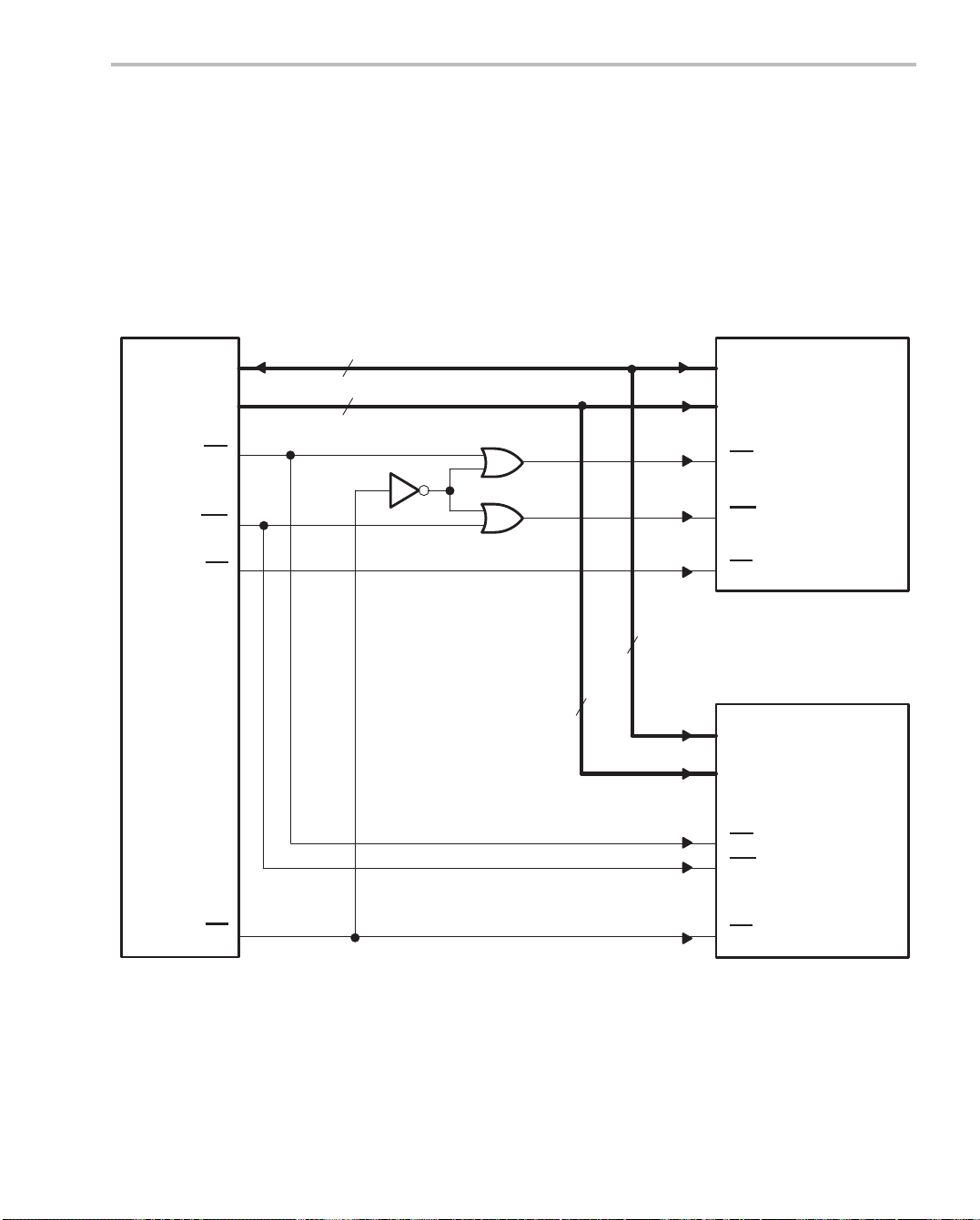
toggled between local memory and global memory . For example, in the system
of Figure 4–6, when GREG = XXXXXXXX00000000
(no global memory), the
2
local data RAM is fully accessible; when GREG = XXXXXXXX10000000
global memory), the local data RAM is not accessible.
Figure 4–6. Using 8000h–FFFFh for Local and Global External Memory
Global Data Memory
(all
2
’C2xx
16
D15–D0 D15–D0
RD
WE
DS
16
16
16
Local data RAM
A15–A0A15–A0
OE
WE
CE
Global data RAM
A15–A0
D15–D0
8000h–FFFFh
8000h–FFFFh
BR
OE
WE
CE
Memory and I/O Spaces
4-13
Page 76

Boot Loader
4.5 Boot Loader
This section applies to ’C2xx devices that have an on-chip boot loader. The
boot loader is used for booting software from an 8-bit external ROM to a 16-bit
external RAM at reset (see Figure 4–7). The source for your program is an external ROM located in external global data memory. The destination for the
boot loaded program is RAM in program space. The main purpose of the boot
loader is to provide you with the ability to use low-cost, simple-to-use 8-bit
EPROMs with the 16-bit ’C2xx.
Figure 4–7. Simplified Block Diagram of Boot Loader Operation
The code for the boot loader is stored on chip. Using the boot loader requires
several steps: choosing an EPROM, connecting and programming the
EPROM, enabling the boot loader program, and finally, booting.
4.5.1 Choosing an EPROM
The code that you want boot loaded must be stored in non-volatile external
memory; usually, this code is stored in an EPROM. Most standard EPROMs
can be used. At reset, the processor defaults to the maximum number of software wait states to accommodate slow EPROMs.
’C2xx
16
8
EPROM
(program source)
Mapped in global data
memory space
RAM
(program destination)
Written starting at
address 0000h
4-14
The maximum size for the EPROM is 32K words × 8 bits, which accommodates a program of up to 16K words 16 bits. However, you could use the
boot loader to load your own boot software to get around this limit or to perform
a different type of boot.
Recommended EPROMs include the 27C32, 27C64, 27C128, and 27C256.
Page 77
4.5.2 Connecting the EPROM to the Processor
To map the EPROM into the global data space at address 8000h, make the
following connections between the processor and the EPROM (refer to
Figure 4–8):
-
Connect the address lines of the processor and the EPROM (see lines
A14–A0 in the figure).
-
Connect the data lines of the processor and the EPROM (see lines D7–D0
in the figure).
-
Connect the processor’s RD pin to the EPROM’s output enable pin (OE
in the figure).
-
Connect the processor’s BR pin to the EPROM’s chip enable pin (CE in
the figure).
Notes:
1) If the EPROM is smaller than 32K words × 8 bits, connect only the address pins that are available on the EPROM.
Boot Loader
2) When the boot loader accesses global memory, along with BR
driven low. Design your system such that the DS
undesired accesses to data memory during the boot loads.
Figure 4–8. Connecting the EPROM to the Processor
’C2xx
A14–A0 A14–A0
RD
BR
15
8
, DS is
signal does not initiate
EPROM
(27C256)
D7–D0D7–D0
OE
CE
Memory and I/O Spaces
4-15
Page 78

Boot Loader
4.5.3 Programming the EPROM
T exas Instruments fixed-point development tools provide the utilities to generate the boot ROM code. (For an introduction to the procedure for generating
boot loader code, see Appendix C,
need to do the programming, use the following procedure.
Store the following to the EPROM:
-
Destination address. Store the destination address in the first two bytes
of the EPROM—store the high-order byte of the destination address at
EPROM address 8000h and store the low-order byte at EPROM address
8001h.
-
Program length. Store N (the length of your program in bytes) in the next
two bytes in EPROM. Use this calculation to determine N:
N = ((number of bytes to be transferred)/2) – 1
Store the high-order N byte at EPROM address 8002h and the low-order N
byte at EPROM address 8003h.
Program Examples
.) However, should you
-
Program. Store the program, one byte at a time, beginning at EPROM address 8004h.
Each word in the program must be divided into two bytes in the EPROM;
store the high-order byte first and store the low-order byte second. For example, if the first word were 813Fh, you would store 81h into the first byte
(at 8004h) and 3Fh into the second byte (at 8005h). Then, you would store
the high byte of the next word at address 8006h.
Notes:
1) Do not include the first four bytes of the EPROM in your calculation of
the length (N). The boot loader uses N beginning at the fifth byte of the
EPROM.
2) Make sure the first part of the program on the EPROM contains code for
the reset and interrupt vectors. These vectors must be stored in the destination RAM first, so that they can be fetched from program-memory addresses 0000h–003Fh. The reset vector will be fetched from 0000h. For
a list of all the assigned vector locations, see subsection 5.6.2,
T able
, on page 5-16.
Interrupt
4-16
Page 79

Boot Loader
Figure 4–9 shows how to store a 16-bit program into the 8-bit EPROM. A subscript h (for example, on Word1
example, on Word1
) indicates the low byte.
l
) indicates the high-byte and a subscript l (for
h
Figure 4–9. Storing the Program in the EPROM
16-Bit Program 8-Bit EPROM
15 8 7 0 Address 7 0
Word1
h
Word2
h
•. • 8002h Length N
• • 8003h Length N
• • 8004h Word1
Wordn
h
Word1
Word2
Wordn
l
l
l
8000h Destination
8001h Destination
h
8005h W ord1
8006h Word2
8007h W ord2
••
••
••
nnnEh Wordn
nnnFh Wordn
l
h
l
h
l
h
l
h
l
4.5.4 Enabling the Boot Loader
To enable the boot loader, tie the BOOT pin low and reset the device. The
pin is sampled only at reset. If you don’t want to use the boot loader,
BOOT
tie BOOT
Three main conditions occur at reset that ensure proper operation of the boot
loader:
-
-
-
After a hardware reset, the processor either executes the boot loader software
or skips execution of the boot loader, depending on the level on the BOOT
-
-
high before initiating a reset.
All maskable interrupts are globally disabled (INTM bit = 1).
On-chip DARAM block B0 is mapped to data space (CNF bit = 0).
Seven wait states are selected for program and data spaces.
If BOOT is low, the processor branches to the location of the on-chip boot
loader program.
If BOOT is high, the processor begins program execution at the address
pointed to by the reset vector at address 0000h in program memory.
Memory and I/O Spaces
pin:
4-17
Page 80

Boot Loader
4.5.5 Boot Loader Execution
Once the EPROM has been programmed and installed, and the boot loader
has been enabled, the processor automatically boots the program from
EPROM at startup. If you need to reboot the processor during operation, bring
the RS
When the processor executes the boot loader, the program first enables the
full 32K words of global data memory by setting the eight LSBs of the GREG
register to 80h. Next, the boot loader copies your program from the EPROM
in global data space to the RAM in program space through a five step process
(refer to Figure 4–10):
1) The boot loader loads the first two bytes from the EPROM and uses this
2) The boot loader loads the next two bytes to determine the length of the
3) The boot loader transfers the next two bytes. It loads the high byte first and
pin low to cause a hardware reset.
word as the destination address for the code. (In Figure 4–10, the
destination is 0000h.)
code.
the low byte second, combines the two bytes into one word, stores the new
word in the destination memory location, and then increments the source
and destination addresses.
4-18
4) The boot loader checks to see if the end of the program has been reached:
J
If the end is reached, the boot loader goes on to step 5.
J
If the end is not reached, the boot loader repeats steps 3 and 4.
5) The boot loader disables the entire global memory and then forces a
branch to the reset vector at address 0000h in program memory . Once the
boot loader finishes operation, the processor switches the on-chip boot
loader out of the memory map.
Note:
During the boot load, data is read using the low-order eight data lines
(D7–D0). The upper eight data lines are not used by the boot loader code.
Page 81

Boot Loader
Figure 4–10. Program Code Transferred From 8-Bit EPROM to 16-Bit RAM
8-Bit EPROM 16-Bit RAM
Address 7 0 Address 15 8 7 0
8000h Destination
8001h Destinationl = 00h • Word2
8002h Length N
8003h Length N
8004h Word1
8005h Word1
8006h Word2
8007h Word2
••
••
••
nnnEh Wordn
nnnFh Wordn
= 00h 0000h Word1
h
h
l
h
l
h
l
h
l
••. •
•• •
nnnEh • •
nnnFh Wordn
h
h
h
Word1
Word2
Wordn
l
l
l
The ’C2xx fetches its interrupt vectors from program-memory locations
0000h–003Fh (the reset vector is fetched from 0000h). Make sure that the interrupt vectors are stored at the top of the EPROM, so that they will be transferred to addresses 0000h–003Fh in the RAM (see Figure 4–1 1). Each interrupt vector is a branch instruction, which requires four 8-bit words, and there
is space for 32 interrupt vectors. Therefore, the first 128 words to be transferred from the EPROM should be the interrupt vectors.
Memory and I/O Spaces
4-19
Page 82
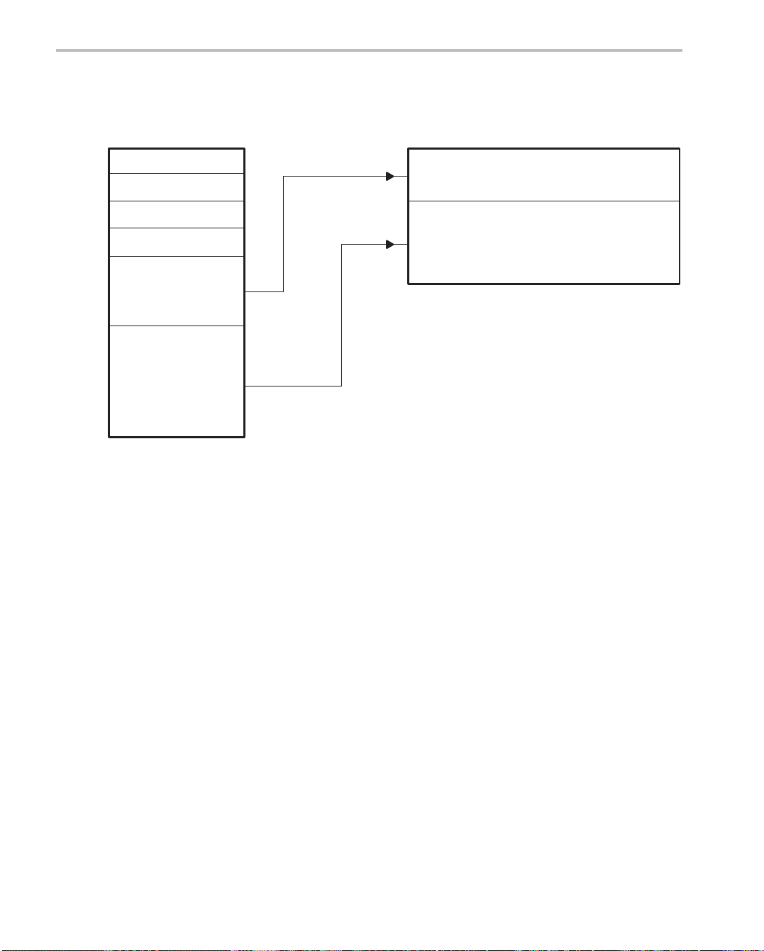
Boot Loader
Figure 4–11.Interrupt Vectors Transferred First During Boot Load
8000h
8001h
8002h
8003h
8004h
8083h
8084h
nnnFh
8-bit EPROM
in global data memory
Destination
Destination
Length N
Length N
(00)
h
(00)
l
h
l
Interrupt vectors
Program code
16-bit RAM
in program memory
0000h
Interrupt vectors
003Fh
0040h
Program code
nnnFh
4-20
Page 83

Boot Loader
4.5.6 Boot Loader Program
*********************************************************************************
* TMS320C2xx Boot Loader Program *
* *
* This code sets up and executes boot loader code that loads program *
* code from location 8000h in external global data space and transfers it *
* to the destination address specified by the first word read from locations *
* 8000h and 8001h. *
*********************************************************************************
.length 60
GREG .set 5h ; The GREG Register
SRC .set 8000h ; Source address
DEST .set 60h ; Destination address
LENGTH .set 61h ; Code length
TEMP .set 62h ; Temporary storage
HBYTE .set 63h ; Temporary storage for upper half of 16–bit word
CODEWORD .set 64h ; Hold program code word
.sect ”bootload”
*
* Initialization
*
BOOT LDP #0 ; Set the data page to 0 (load DP with 0)
SPLK #2E00h,TEMP ; Set ARP = 1, OVM = 1, INTM = 1, DP = 0
LST #0,TEMP
SPLK #21FCh,TEMP ; Set ARB = 1, CNF = 0, SXM = 0, XF = 1, PM = 0
LST #1,TEMP
SPLK #80h,GREG ; Designate locations 8000–FFFFH as global data
; space
* * * * * * * * * * * * * * * * * * * * * * * * * * * * * * * * * * * * * *
* BOOT LOAD FROM 8–BIT MEMORY. MOST SIGNIFICANT BYTE IS FIRST *
* * * * * * * * * * * * * * * * * * * * * * * * * * * * * * * * * * * * * *
*
* Determine destination address
*
ADDR LAR AR1,#SRC ; AR1 points to global address 8000h
LACC *+,8 ; Load ACC with high byte shifted left by 8 bits
SACL HBYTE ; Store high byte
LACL *+ ; Load ACC with low byte of destination
AND #0FFH ; Mask off upper 24 bits.
OR HBYTE ; OR ACC with high byte to form 16-bit
; destination address
SACL DEST ; Store destination address
*
* Determine length of code to be transferred
*
LEN LACC *+,8 ; Load ACC with high byte shifted left by 8 bits
SACL HBYTE ; Store high byte
LACL *+ ; Load ACC with low byte of length
AND #0FFH ; Mask off upper 24 bits.
OR HBYTE ; OR ACC with high byte to form 16-bit length
SACL LENGTH ; Store length
LAR AR0,LENGTH ; Load AR0 with length to be used for BANZ
Memory and I/O Spaces
4-21
Page 84

Boot Loader
*
* Transfer code
*
LOOP LACC *+,8 ; Load ACC with high byte of code shifted by 8 bits
SACL HBYTE ; Store high byte
LACL *+,AR0 ; Load ACC with low byte of code
AND #0FFH ; Mask off upper 24 bits
OR HBYTE ; OR ACC with high byte to form 16-bit code word
SACL CODEWORD ; Store code word
LACL DEST ; Load destination address
TBLW CODEWORD ; Transfer code to destination address
ADD #1 ; Add 1 to destination address
SACL DEST ; Save new address
BANZ LOOP,AR1 ; Determine if end of code is reached
SPLK #0,GREG ; Disable entire global memory
INTR 0 ; Branch to reset vector and execute code.
.END
Note:
The INTR instruction in the boot loader program causes the processor to
push a return address onto the stack, but the device does not use a RET to
return to this address. Therefore, your program must execute a POP
instruction to get the address off the stack.
4-22
Page 85

4.6 I/O Space
The ’C2xx supports an I/O address range of 64K 16-bit words. Figure 4–12
shows the ’C2xx I/O address map.
Figure 4–12. I/O Address Map for the ’C2xx
0000h
I/O Space
’C2xx I/O
External
On-chip space
FEFFh
FF00h
FF0Fh
FF10h
FFFFh
Reserved for
test/emulation
I/O-mapped
registers and
reserved addresses
Memory and I/O Spaces
4-23
Page 86

I/O Space
The map has three main sections of addresses:
-
Addresses 0000h–FEFFh allow access to off-chip peripherals typically
used in DSP applications, such as digital-to-analog and analog-to-digital
converters.
-
Addresses FF00h–FF0Fh are mapped to on-chip I/O space. These addresses are reserved for test purposes and should not be used.
-
Addresses FF10h–FFFFh are also mapped to on-chip I/O space. These
addresses are used for other reserved space and for the on-chip I/Omapped registers. For ’C2xx devices other than the ’C209, T able 4–4 lists
the registers mapped to on-chip I/O space. For the I/O-mapped registers
on the ’C209, see Section 11.2, on page 11-5.
Do Not Write to Reserved Addresses
T o avoid unpredictable operation of the processor, do not write to
I/O addresses FF00h–FF0Fh or any reserved I/O address in the
range FF10–FFFFh (that is, any address not designated for an
on-chip peripheral.)
Table 4–4. On-Chip Registers Mapped to I/O Space
I/O Address Name Description
FFE8h CLK CLK register
FFECh ICR Interrupt control register
FFF0h SDTR Synchronous serial port transmit and receive register
FFF1h SSPCR Synchronous serial port control register
FFF4h ADTR Asynchronous serial port transmit and receive register
FFF5h ASPCR Asynchronous serial port control register
FFF6h IOSR Input/output status register
FFF7h BRD Baud rate divisor register
FFF8h TCR Timer control register
FFF9h PRD Timer period register
FFFAh TIM Timer counter register
FFFCh WSGR Wait-state generator control register
4-24
Note: This table does not apply to the ’C209. For the I/O-mapped registers on the ’C209,
see Section 11.2 on page 11-5.
Page 87

4.6.1 Accessing I/O Space
All I/O words (external I/O ports and on-chip I/O registers) are accessed with
the IN and OUT instructions. Accesses to external parallel I/O ports are multiplexed over the same address and data buses for program and data-memory
accesses. These accesses are distinguished from external program and datamemory accesses by IS
you use 8-bit peripherals, you can use either the higher or lower eight lines of
the data bus to suit a particular application.
I/O Space
going low. The data bus is 16 bits wide; however, if
Y ou can use RD
an external peripheral. You can also use the WE
with chip-select logic to generate an output-enable signal for
signal with chip-select logic
to generate a write-enable signal for an external peripheral. As an example of
interfacing to external I/O space, Figure 4–13 shows interface circuitry for
eight input bits and eight output bits. Note that the decode section is simplified
if fewer I/O ports are used.
Memory and I/O Spaces
4-25
Page 88

I/O Space
Figure 4–13. I/O Port Interface Circuitry
A0
A1
A2
A3
’C2xx DSP
1
2
3
6
5 V
4
5
I/O port address decoder
A
B
C
G1
G2A
G2B
74AC138
Y0
Y1
Y2
Y3
Y4
Y5
Y6
Y7
15
14
13
12
11
10
9
7
Port 0
Port 1
Port 2
Port 3
Port 4
Port 5
Port 6
Port 7
D0
D1
D2
D3
D4
D5
D6
D7
WE
18
1Y1
16
1Y2
14
1Y3
12
1Y4
9
2Y1
7
2Y2
5
2Y3
3
2Y4
IS
5 V
74AC244
8-bit input port at
I/O address 0000h
3
D1
4
D2
7
D3
8
D4
13
D5
14
D6
17
D7
18
D8
11
CLK
1
CLR
74AC273
8-bit output latch
at I/O address 0001h
1A1
1A2
1A3
1A4
2A1
2A2
2A3
2A4
1G
2G
Q1
Q2
Q3
Q4
Q5
Q6
Q7
Q8
2
4
6
8
11
13
15
17
2
5
6
9
12
15
16
19
1
19
Input bit 0
Input bit 1
Input bit 2
Input bit 3
Input bit 4
Input bit 5
Input bit 6
Input bit 7
Output bit 0
Output bit 1
Output bit 2
Output bit 3
Output bit 4
Output bit 5
Output bit 6
Output bit 7
4-26
Page 89

Direct Memory Access Using the HOLD Operation
4.7 Direct Memory Access Using the HOLD Operation
The ’C2xx HOLD operation allows direct-memory access to external program,
data, and I/O spaces. The process is controlled by two signals:
-
HOLD. An external device can drive the HOLD/INT1 pin low to request
control over the external buses. If the HOLD/INT1 interrupt line is enabled,
this triggers an interrupt.
-
HOLDA. In response to a HOLD interrupt, software logic can cause the
processor to issue a HOLD
it is relinquishing control of its external lines. Upon HOLDA
address signals (A15–A0), data signals (D15–D0), and memory-control
signals (PS
, DS, BR, IS, STRB, R/W, RD, WE) are placed in high imped-
ance.
Following a negative edge on the HOLD/INT1 pin, if interrupt line HOLD/INT1
is enabled, the CPU branches to address 0002h (this branch could also be accomplished with an INTR 1 instruction). Here the CPU fetches the interrupt
vector and follows it to the interrupt service routine. If you wish to use this routine for HOLD operations and also for the interrupt INT1
by this routine will depend on the value of the MODE bit:
acknowledge (HOLDA pin low), to indicate that
, the external
, the tasks carried out
-
MODE = 1. When the CPU detects a negative edge on HOLD/INT1, it
finishes executing the current instruction (or repeat operation) and then
forces program control to the interrupt service routine. The interrupt service routine, after successfully testing for MODE = 1, performs the tasks
for INT1
-
MODE = 0. Interrupt line INT1 is both negative- and positive-edge sensi-
.
tive. When the CPU detects the negative edge, it finishes executing the
current instruction (or repeat operation) and then forces program control
to the interrupt service routine. This routine, after successfully testing for
MODE = 0, executes an IDLE instruction. Upon IDLE, HOLDA
is asserted
and the external lines are placed in high impedance. Only after detecting
a rising edge on the HOLD
deasserts HOLDA
, and returns the external lines to their normal states.
/INT1 pin, the CPU exits the IDLE state,
Example 4–1 shows an interrupt service routine that tests the MODE bit and
acts accordingly . Note that the IDLE instruction should be placed inside the interrupt service routine to issue HOLDA
code disables all maskable interrupts except HOLD
ery of HOLDA
and the buses. Any other sequence of CPU code will cause un-
. Also note that the interrupt program
/INT1 to allow safe recov-
desirable bus control and is not recommended. (Interrupt operation is explained in detail in Section 5.6 on page 5-15.)
Memory and I/O Spaces
4-27
Page 90

Direct Memory Access Using the HOLD Operation
Example 4–1. An Interrupt Service Routine Supporting INT1 and HOLD
ICR .set 0FFECh ;Define interrupt control register in I/O space.
ICRSHDW .set 060h ;Define ICRSHDW in scratch pad location.
* Interrupt vectors *
reset B main ;0 – reset , Branch to main program on reset.
Int1h B int1_hold ;1 – external interrupt 1 or HOLD.
main: SPLK #0001h,imr ;Enable HOLD/INT1 interrupt line.
wait: B wait
*********Interrupt service routine for HOLD logic*****************************
int1_hold:
.mmregs ;Include c2xx memory–mapped registers.
.space 40*16 ;Fill 0000 between vectors and main program.
CLRC INTM
; Perform any desired context save.
LDP #0 ;Set data–memory page to 0.
IN ICRSHDW, ICR ;Save the contents of ICR register.
LACL #010h ;Load accumulator (ACC) with mask for MODE bit.
AND ICRSHDW ;Filter out all bits except MODE bit.
BCND int1, neq ;Branch if MODE bit is 1, else in HOLD mode.
LACC imr, 0 ;Load ACC with interrupt mask register.
SPLK #1, imr ;Mask all interrupts except interrupt1/HOLD.
IDLE ;Enter HOLD mode. Issues HOLDA, and puts
;buses in high impedance. Wait until
;rising edge is seen on HOLD/INT1 pin.
SPLK #1, ifr ;Clear HOLD/INT1 flag in interrupt flag register
;to prevent re–entering HOLD mode.
SACL imr ;Restore interrupt mask register.
; Perform necessary context restore.
CLRC INTM ;Enable all interrupts.
RET ;Return from HOLD interrupt.
int1: NOP ;Replace these NOPs with desired int1 interrupt
4-28
NOP ;service routine.
; Perform necessary context restore.
CLRC INTM ;Enable all interrupts.
RET ;Return from interrupts.
Page 91

Direct Memory Access Using the HOLD Operation
Here are three valid methods for exiting the IDLE state, thus deasserting
HOLDA
-
-
-
and restoring the buses to normal operation:
Cause a rising edge on the HOLD/INT1 pin when MODE = 0.
Assert system reset at the reset pin.
Assert the nonmaskable interrupt NMI at the NMI pin.
If reset or NMI
occurs while HOLDA is asserted, the CPU will deassert HOLDA
regardless of the level on the HOLD/INT1 pin. Therefore, to avoid further conflicts in bus control, the system hardware logic should restore HOLD
state.
4.7.1 HOLD During Reset
The HOLD logic can be used to put the buses in a high-impedance state at
power-on or reset. This feature is useful in extending the DSP memory control
to external processors. If HOLD
tion occurs internally , but HOLDA
is driven low during reset, normal reset opera-
will be asserted, placing all buses and control lines in a high-impedance state. Upon release of both HOLD
execution starts from program location 0000h.
Either of the following conditions will cause the processor to deassert HOLDA
and return the buses to a normal state:
-
HOLD is deasserted before reset is deasserted. See Figure 4–14. This
is the normal recovery condition after a HOLD operation. After the HOLD
signal goes high, the HOLDA signal will be deasserted, and the buses will
assume normal states.
Figure 4–14. HOLD Deasserted Before Reset Deasserted
to a high
and RS,
RS
HOLD
HOLDA
-
Reset is deasserted before HOLD is deasserted. See Figure 4–15. The
CPU will deassert HOLDA
regardless of the HOLD signal after the 16 clock
cycles required for normal reset operation. Along with the HOLDA
the buses will assume normal states. The external system hardware logic
should restore the HOLD
signal to a high state to avoid conflicts in HOLD
logic.
Memory and I/O Spaces
signal,
4-29
Page 92

Direct Memory Access Using the HOLD Operation
Direct Memory Access Using the HOLD Operation
Figure 4–15. Reset Deasserted Before HOLD Deasserted
RS
HOLD
HOLDA
4-30
Page 93

4.8 Device-Specific Information
For ’C2xx devices other than the ’C209, this section mentions the presence
or absence of the boot loader and HOLD features, shows address maps, and
explains the contents and configuration of the program-memory and datamemory maps. For details about the memory and I/O spaces of the ’C209, see
Section 11.2 on page 11-5.
4.8.1 TMS320C203 Address Maps and Memory Configuration
The ’C203 has a ’C2xx on-chip boot loader and supports the ’C2xx HOLD
operation. Figure 4–16 shows the ’C203 address map.
The on-chip program and data memory available on the ’C203 consists of:
-
DARAM B0 (256 words, for program or data memory)
-
DARAM B1 (256 words, for data memory)
-
DARAM B2 (32 words, for data memory)
Device-Specific Information
Memory and I/O Spaces
4-31
Page 94

Device-Specific Information
Figure 4–16. ’C203 Address Map
’C203 I/O
0000h
003Fh
’C203 Program ’C203 Data
Interrupts (external)
0000h
Memory-mapped
registers and
005Fh
0060h
007Fh
reserved addresses
On-chip
DARAM B2
0000h
0080h
Reserved
External
01FFh
0200h
02FFh
0300h
03FFh
On-chip DARAM
‡
B0
(CNF = 0);
Reserved (CNF = 1)
On-chip
DARAM B1
§
External
0400h
Reserved
07FFh
0800h
External
FDFFh
FE00h
Reserved (CNF = 1);
7FFFh
8000h
External (CNF = 0)
FEFFh
FF00h
FFFFh
†
When CNF = 1, addresses FE00h–FEFFh and FF00h–FFFFh are mapped to the same physical block (B0) in program-memory
space. For example, a write to FE00h will have the same effect as a write to FF00h. For simplicity , addresses FE00h–FEFFh
are referred to here as reserved when CNF = 1.
‡
When CNF = 0, addresses 0100h–01FFh and 0200h–02FFh are mapped to the same physical block (B0) in data-memory
space. For example, a write to 0100h will have the same effect as a write to 0200h. For simplicity , addresses 0100h–01FFh are
referred to here as reserved.
§
Addresses 0300h–03FFh and 0400h–04FFh are mapped to the same physical block (B1) in data-memory space. For example,
a write to 0400h has the same effect as a write to 0300h. For simplicity, addresses 0400h–04FFh are referred to here as
reserved.
On-chip DARAM
†
B0
(CNF = 1);
External (CNF = 0)
FFFFh
External
(local and/or global)
FEFFh
FF00h
FF0Fh
FF10h
FFFFh
Reserved for
test/emulation
I/O-mapped
registers and
reserved addresses
4-32
Page 95

Device-Specific Information
DARAM blocks B1 and B2 are fixed, but DARAM block B0 may be mapped to
program space or data space, depending on the value of the CNF bit (bit 12
of status register ST1):
-
CNF = 0. B0 is mapped to data space and is accessible at data addresses
0200h–02FFh. Note that the addressable external
program
memory in-
creases by 512 words.
-
CNF = 1. B0 is mapped to program space and is accessible at program
addresses FF00h–FFFFh.
At reset, CNF = 0.
Table 4–5 shows the program-memory options for the ’C203; Table 4–6 lists
the data-memory options. Note these facts:
-
Program-memory addresses 0000h–003Fh are used for the interrupt
vectors.
-
Data-memory addresses 0000h–005Fh contain on-chip memory-mapped
registers and reserved memory.
-
Two other on-chip data-memory ranges are always reserved:
0080h–01FFh and 0400h–07FFh.
Do Not Write to Reserved Addresses
T o avoid unpredictable operation of the processor, do not write to
any addresses labeled Reserved. This includes any data-memory
address in the range 0000h–005Fh that is not designated for an
on-chip register and any I/O address in the range FF00h–FFFFh
that is not designated for an on-chip register.
Table 4–5. ’C203 Program-Memory Configuration Options
CNF DARAM B0 External Reserved
0 – 0000h–FFFFh –
1 FF00h–FFFFh 0000h–FDFFh FE00h–FEFFh
Memory and I/O Spaces
4-33
Page 96

Device-Specific Information
Table 4–6. ’C203 Data-Memory Configuration Options
DARAM B0
CNF
0 0200–02FF 0300–03FF 0060–007F 0800–FFFF 0000–005F
1 – 0300–03FF 0060–007F 0800–FFFF 0000–005F
(hex)
DARAM B1
(hex)
DARAM B2
(hex)
4.8.2 TMS320C204 Address Maps and Memory Configuration
The ’C204 does not have an on-chip boot loader, but it does support the ’C2xx
HOLD operation. Figure 4–16 shows the ’C204 address map. The on-chip
program and data memory available on the ’C204 consists of:
-
ROM (4K words, for program memory)
-
DARAM B0 (256 words, for program or data memory)
-
DARAM B1 (256 words, for data memory)
-
DARAM B2 (32 words, for data memory)
External
(hex)
Reserved
(hex)
0080–01FF
0400–07FF
0080–02FF
0400–07FF
4-34
Page 97

Figure 4–17. ’C204 Address Map
Device-Specific Information
’C204 I/O
External
0000h
003Fh
1000h
0FFFh
’C204 Program ’C204 Data
Interrupts (on-chip)
= 0)
(MP/MC
Interrupts (external)
(MP/MC
= 1)
On-chip ROM
(MP/MC
= 0)
External
(MP/MC
= 1)
0000h
005Fh
0060h
007Fh
0080h
Memory-mapped
registers and
reserved addresses
On-chip
DARAM B2
Reserved
01FFh
External
0200h
02FFh
0300h
03FFh
On-chip DARAM
‡
B0
(CNF = 0);
Reserved (CNF = 1)
On-chip
DARAM B1
0000h
§
0400h
Reserved
07FFh
0800h
FDFFh
FE00h
Reserved (CNF = 1);
External (CNF = 0)
FEFFh
FF00h
FFFFh
†
When CNF = 1, addresses FE00h–FEFFh and FF00h–FFFFh are mapped to the same physical block (B0) in program-memory
space. For example, a write to FE00h will have the same effect as a write to FF00h. For simplicity , addresses FE00h–FEFFh
are referred to here as reserved when CNF = 1.
‡
When CNF = 0, addresses 0100h–01FFh and 0200h–02FFh are mapped to the same physical block (B0) in data-memory
space. For example, a write to 0100h will have the same effect as a write to 0200h. For simplicity , addresses 0100h–01FFh are
referred to here as reserved.
§
Addresses 0300h–03FFh and 0400h–04FFh are mapped to the same physical block (B1) in data-memory space. For example,
a write to 0400h has the same effect as a write to 0300h. For simplicity, addresses 0400h–04FFh are referred to here as
reserved.
On-chip DARAM
†
B0
(CNF = 1);
External (CNF = 0)
7FFFh
8000h
External
(local and/or global)
FFFFh
External
FEFFh
FF00h
FF0Fh
FF10h
FFFFh
Reserved for
test/emulation
I/O-mapped
registers and
reserved addresses
Memory and I/O Spaces
4-35
Page 98

Device-Specific Information
Y ou select or deselect the ROM by changing the level on the MP/MC pin at reset:
-
MP/MC = 0 at reset. The device is configured as a microcomputer. The
on-chip ROM is enabled and is accessible at addresses 0000h–0FFFh.
The device fetches the reset vector from on-chip ROM.
-
MP/MC = 1 at reset. The device is configured as a microprocessor, and
addresses 0000h–0FFFh are used to access external memory. The device fetches the reset vector from external memory.
Regardless of the value of MP/MC
, the ’C2xx fetches its reset vector at location
0000h of program memory.
DARAM blocks B1 and B2 are fixed, but DARAM block B0 may be mapped to
program space or data space, depending on the value of the CNF bit (bit 12
of status register ST1):
-
CNF = 0. B0 is mapped to data space and is accessible at data addresses
0200h–02FFh. Note that the addressable external
program
memory in-
creases by 512 words.
-
CNF = 1. B0 is mapped to program space and is accessible at program
addresses FF00h–FFFFh.
At reset, CNF = 0.
Table 4–7 lists the available program memory configurations for the ’C204;
Table 4–8 lists the data-memory configurations. Note these facts:
-
Program-memory addresses 0000h–003Fh are used for the interrupt
vectors.
-
Data-memory addresses 0000h–005Fh contain on-chip memory-mapped
registers and reserved memory.
-
Two other on-chip data-memory ranges are always reserved:
0080h–01FFh and 0400h–07FFh.
4-36
Do Not Write to Reserved Addresses
T o avoid unpredictable operation of the processor, do not write to
any addresses labeled Reserved. This includes any data-memory
address in the range 0000h–005Fh that is not designated for an
on-chip register and any I/O address in the range FF00h–FFFFh
that is not designated for an on-chip register.
Page 99

Table 4–7. ’C204 Program-Memory Configuration Options
Device-Specific Information
ROM
MP/MC CNF
0 0 0000–0FFF – 1000–FFFF –
0 1 0000–0FFF FF00–FFFF 1000–FDFF FE00–FEFF
1 0 – – 0000–FFFF –
1
1 – FF00–FFFF 0000–FDFF FE00–FEFF
(hex)
DARAM B0
(hex)
External
(hex)
Table 4–8. ’C204 Data-Memory Configuration Options
DARAM B0
CNF
0 0200–02FF 0300–03FF 0060–007F 0800–FFFF 0000–005F
1 – 0300–03FF 0060–007F 0800–FFFF 0000–005F
(hex)
DARAM B1
(hex)
DARAM B2
(hex)
External
(hex)
Reserved
(hex)
Reserved
(hex)
0080–01FF
0400–07FF
0080–02FF
0400–07FF
Memory and I/O Spaces
4-37
Page 100

Chapter 5
Program Control
This chapter discusses the processes and features involved in controlling the
flow of a program on the ’C2xx.
Program control involves controlling the order in which one or more blocks of
instructions are executed. Normally, the flow of a program is sequential: the
’C2xx executes instructions at consecutive program-memory addresses. At
times, a program must branch to a nonsequential address and then execute
instructions sequentially at that new location. For this purpose, the ’C2xx supports branches, calls, returns, repeats, and interrupts.
The ’C2xx also provides a power-down mode, which halts internal program
flow and temporarily lowers the power requirements of the ’C2xx.
Topic Page
5.1 Program-Address Generation 5-2. . . . . . . . . . . . . . . . . . . . . . . . . . . . . . . . . .
5.2 Pipeline Operation 5-7. . . . . . . . . . . . . . . . . . . . . . . . . . . . . . . . . . . . . . . . . . . .
5.3 Branches, Calls, and Returns 5-8. . . . . . . . . . . . . . . . . . . . . . . . . . . . . . . . . .
5.4 Conditional Branches, Calls, and Returns 5-10. . . . . . . . . . . . . . . . . . . . . .
5.5 Repeating a Single Instruction 5-14. . . . . . . . . . . . . . . . . . . . . . . . . . . . . . . .
5.6 Interrupts 5-15. . . . . . . . . . . . . . . . . . . . . . . . . . . . . . . . . . . . . . . . . . . . . . . . . . .
5.7 Reset Operation 5-33. . . . . . . . . . . . . . . . . . . . . . . . . . . . . . . . . . . . . . . . . . . . .
5.8 Power-Down Mode 5-36. . . . . . . . . . . . . . . . . . . . . . . . . . . . . . . . . . . . . . . . . . .
5-1
 Loading...