查询TMS27C210A供应商
TMS27C210A 65536 BY 16-BIT UV ERASABLE
TMS27PC210A 65536 BY 16-BIT
PROGRAMMABLE READ-ONLY MEMORIES
SMLS310D– NOVEMBER 1990 – REVISED SEPTEMBER 1997
D
Organization...65536 by 16 Bits
D
Single 5-V Power Supply
D
Operationally Compatible With Existing
Megabit EPROMs
D
40-Pin Dual-In-Line Package and 44-Lead
Plastic Leaded Chip Carrier
D
All Inputs/Outputs Fully TTL Compatible
D
±10% VCC Tolerance
D
Maximum Access/Minimum Cycle Time
’27C/PC210A-10 100 ns
’27C/PC210A-12 120 ns
’27C/PC210A-15 150 ns
’27C/PC210A-20 200 ns
’27C/PC210A-25 250 ns
D
16-Bit Output For Use in
Microprocessor-Based Systems
D
Very High-Speed SNAP! Pulse
Programming
D
Power-Saving CMOS Technology
D
3-State Output Buffers
D
400-mV Minimum DC Noise Immunity With
Standard TTL Loads
D
Latchup Immunity of 250 mA on All Input
and Output Pins
D
No Pullup Resistors Required
D
Low Power Dissipation
– Active...275 mW Worst Case
– Standby...0.55 mW Worst Case
(CMOS-Input Levels)
D
Temperature Range Options
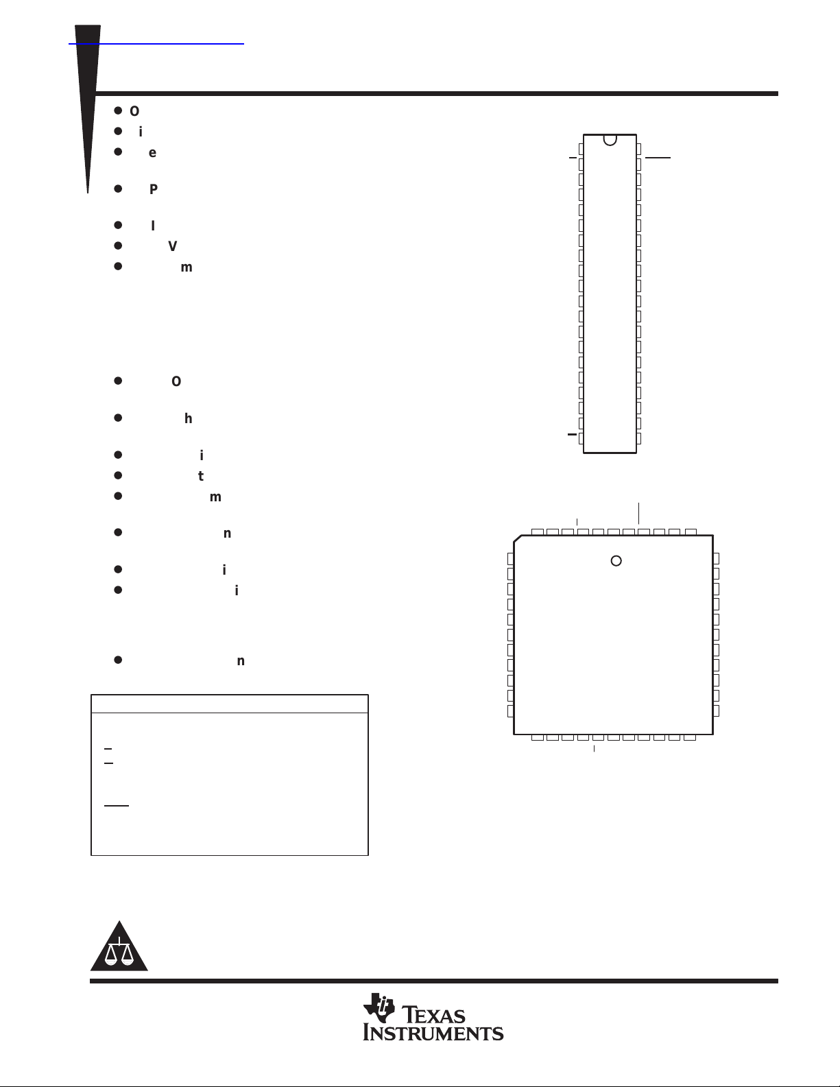
PIN NOMENCLATURE
A0–A15 Address Inputs
DQ0–DQ15 Inputs (programming)/Outputs
E
G Output Enable
GND Ground
NC No Internal Connection
PGM Program
V
CC
V
PP
Chip Enable
5-V Power Supply
13-V Power Supply
‡
DQ12
DQ11
DQ10
DQ9
DQ8
GND
NC
DQ7
DQ6
DQ5
DQ4
J PACKAGE
(TOP VIEW)
V
1
PP
E
2
DQ15
3
DQ14
4
DQ13
5
DQ12
6
7
DQ11
8
DQ10
9
DQ9
10
DQ8
†
DQ7
DQ6
DQ5
DQ4
DQ3
DQ2
DQ1
DQ0
G
FN PACKAGE
(TOP VIEW)
DQ14
DQ15ENC
5 43 26
20 21 22 23
DQ2
DQ1
11
12
13
14
15
16
17
18
19
20
V
DQ0
GND
DQ13
7
8
9
10
11
†
12
13
14
15
16
17
18 19
DQ3
V
40
PGM
39
NC
38
A15
37
A14
36
A13
35
34
A12
33
A11
32
A10
31
A9
30
GND
29
A8
28
A7
27
A6
26
A5
25
A4
24
A3
23
A2
22
A1
21
A0
CC
PP
V
1
44 43
24 25 26 27 28
G
A0
NC
CC
†
PGMNCA15
42 41 40
A1A2A3
A14
39
38
37
36
35
34
33
32
31
30
29
A4
A13
A12
A11
A10
A9
GND
NC
A8
A7
A6
A5
†
†
Pins 11 and 30 (J package) and pins 12 and 34 (FN
package) must be connected externally to ground.
‡
Only in program mode
Please be aware that an important notice concerning availability, standard warranty, and use in critical applications of
Texas Instruments semiconductor products and disclaimers thereto appears at the end of this data sheet.
PRODUCTION DATA information is current as of publication date.
Products conform to specifications per the terms of Texas Instruments
standard warranty. Production processing does not necessarily include
testing of all parameters.
POST OFFICE BOX 1443 • HOUSTON, TEXAS 77251–1443
Copyright 1997, Texas Instruments Incorporated
1
TMS27C210A 65536 BY 16-BIT UV ERASABLE
TMS27PC210A 65536 BY 16-BIT
PROGRAMMABLE READ-ONLY MEMORIES
SMLS310D– NOVEMBER 1990 – REVISED SEPTEMBER 1997
description
The TMS27C210A series are 65536 by 16-bit (1048576-bit), ultraviolet-light erasable, electrically
programmable read-only memories (EPROMs).
The TMS27PC210A series are 65 536 by 16-bit (1 048576-bit), one-time programmable (OTP) electrically
programmable read-only memories (PROMs).
These devices are fabricated using power-saving CMOS technology for high speed and simple interface with
MOS and bipolar circuits. All inputs (including program data inputs) can be driven by Series 74 TTL circuits
without the use of external pullup resistors. Each output can drive one Series 74 TTL circuit without external
resistors.
The TMS27C210A EPROM is offered in a dual-in-line ceramic package (J suffix) designed for insertion in
mounting hole rows on 15,2-mm (600-mil) centers. The TMS27C210A is offered with two choices of
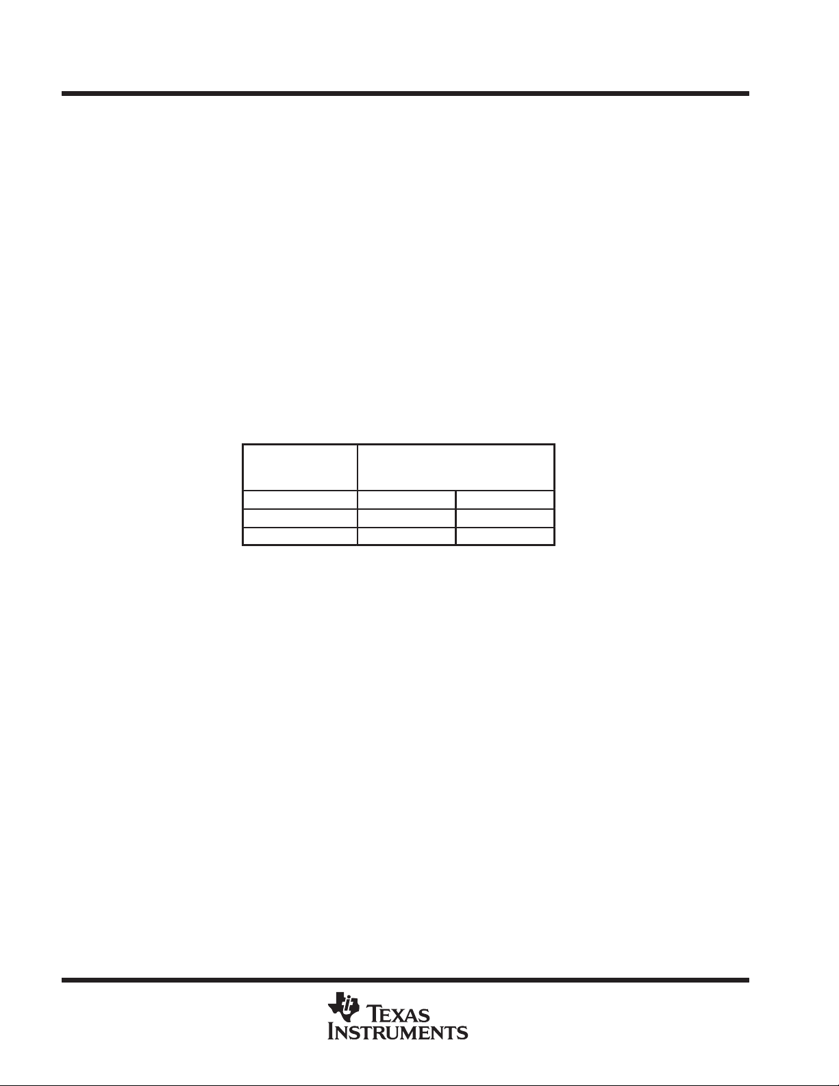
temperature ranges, 0°C to 70°C (JL suffix) and – 40°C to 85°C (JE suffix). See Table 1.
The TMS27PC210A OTP PROM is offered in a 44-pin plastic leaded chip carrier package using 1,25-mm
(50-mil) lead spacing ( FN suffix). The TMS27PC210A is offered with two choices of temperature ranges,
0°C to 70°C (FNL suffix) and –40°C to 85°C (FNE suffix). See Table 1.
Table 1. Temperature Range Suffixes
EPROM
AND
OTP PROM
TMS27C210A-xx JL JE
TMS27PC210A-xx FNL FNE
SUFFIX FOR OPERATING
FREE-AIR TEMPERATURE
RANGES
0°C to 70°C – 40°C to 85°C
These EPROMs and OTP PROMs operate from a single 5-V supply (in the read mode), they are ideal for use
in microprocessor based systems. One other (13 V) supply is needed for programming. All programming signals
are TTL level. For programming outside the system, existing EPROM programmers can be used.
operation
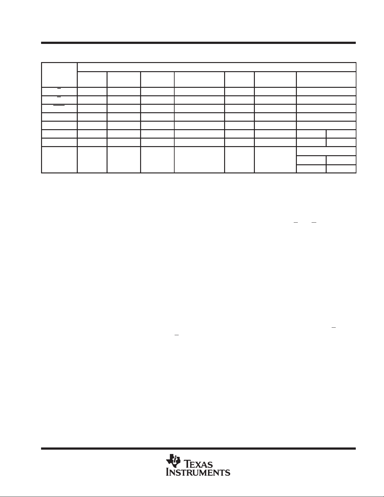
The seven modes of operation for the TMS27C210A and TMS27PC210A are listed in T able 2. The read mode
requires a single 5-V supply . All inputs are TTL level except for V
A9 for signature mode.
during programming (13 V), and 12 V on
PP
2
POST OFFICE BOX 1443 • HOUSTON, TEXAS 77251–1443
TMS27C210A 65536 BY 16-BIT UV ERASABLE
TMS27PC210A 65536 BY 16-BIT
PROGRAMMABLE READ-ONLY MEMORIES
SMLS310D– NOVEMBER 1990 – REVISED SEPTEMBER 1997
Table 2. Operation Modes
†
MODE
FUNCTION
E V
G V
PGM X X X V
V
PP
V
CC
A9 X X X X X X VH‡ VH‡
A0 X X X X X X V
DQ0–DQ15 Data Out Hi-Z Hi-Z Data In Data Out Hi-Z
†
X can be VIL or VIH.
‡
VH = 12 V ±0.5 V.
READ
IL
IL
V
CC
V
CC
OUTPUT
DISABLE
V
IL
V
IH
V
CC
V
CC
STANDBY PROGRAMMING VERIFY
V
IH
X V
V
CC
V
CC
V
IL
IH
IL
V
PP
V
CC
V
IL
V
IL
V
IH
V
PP
V
CC
PROGRAM
INHIBIT
V
IH
X V
X X
V
PP
V
CC
SIGNATURE MODE
IL
MFG DEVICE
97 AB
V
IL
IL
V
CC
V
CC
CODE
V
IH
read/output disable
When the outputs of two or more TMS27C210As or TMS27PC210As are connected in parallel on the same bus,
the output of any particular device in the circuit can be read with no interference from competing outputs of the
other devices. To read the output of a single device, a low level signal is applied to the E
and G pins. All other
devices in the circuit must have their outputs disabled by applying a high level signal to one of these pins.
latchup immunity
Latchup immunity on the TMS27C210A and TMS27PC210A is a minimum of 250 mA on all inputs and outputs.
This feature provides latchup immunity beyond any potential transients at the P .C. board level when the EPROM
is interfaced to industry standard TTL or MOS logic devices. The input/output layout approach controls latchup
without compromising performance or packing density.
For more information see application report SMLA001, “
HVCMOS EPROM Family
”, available through TI Sales Offices.
Design Considerations; Latchup Immunity of the
power down
Active ICC supply current can be reduced from 50 mA to 500 µA by applying a high TTL input on E and to
100 µA by applying a high CMOS input on E
. In this mode all outputs are in the high-impedance state.
erasure (TMS27C210A)
Before programming, the TMS27C210A is erased by exposing the chip through the transparent lid to a high
intensity ultraviolet light (wavelength 2537 Å). The recommended minimum exposure dose (UV intensity ×
exposure time) is 15-W•s/cm
lamp should be located about 2.5 cm above the chip during erasure. After erasure, all bits are in the high state.
Normal ambient light contains the correct wavelength for erasure; therefore, when using the TMS27C210A the
window should be covered with an opaque label.
2
. A typical 12-mW/cm2, filterless UV lamp erases the device in 21 minutes. The
initializing (TMS27PC210A)
The OTP TMS27PC210A PROM is provided with all bits in the logic high state then logic lows are programmed
into the desired locations. Logic lows programmed into an OTP PROM cannot be erased.
POST OFFICE BOX 1443 • HOUSTON, TEXAS 77251–1443
3
TMS27C210A 65536 BY 16-BIT UV ERASABLE
IDENTIFIER
†
TMS27PC210A 65536 BY 16-BIT
PROGRAMMABLE READ-ONLY MEMORIES
SMLS310D– NOVEMBER 1990 – REVISED SEPTEMBER 1997
SNAP! Pulse programming
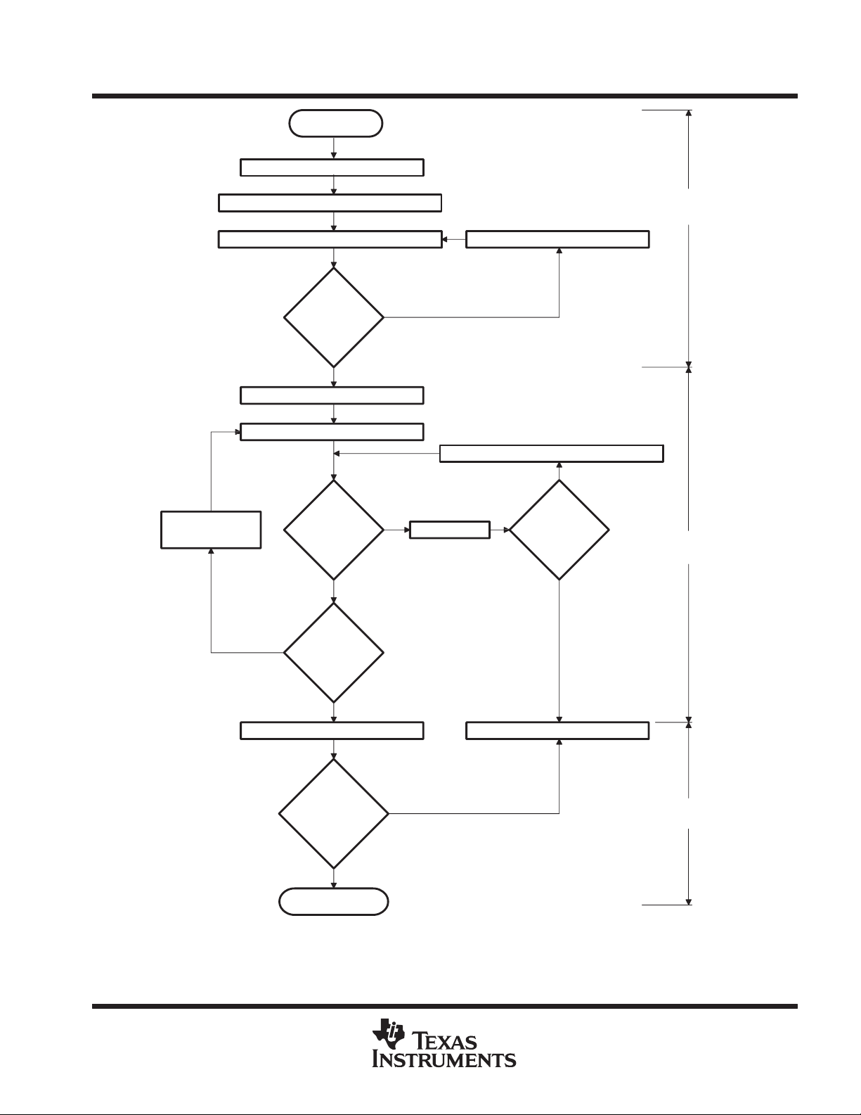
The TMS27C210A and TMS27PC210A are programmed using the TI SNAP! Pulse programming algorithm
(shown in the flow chart in Figure 1), which can program in a nominal time of seven seconds. Actual
programming time varies as a function of the programmer used.
The SNAP! Pulse programming algorithm uses an initial pulse of 100 microseconds (µs) followed by a byte
verification to determine when the addressed byte has been successfully programmed. Up to 10 (ten) 100-µs
pulses per byte are provided before a failure is recognized.
The programming mode is achieved when V
(16 bits) on pins DQ0 through DQ15. Once addresses and data are stable, PGM
= 13 V , VCC = 6.5 V , E = VIL, G = VIH. Data is presented in parallel
PP
is pulsed low.
More than one device can be programmed when the devices are connected in parallel. Locations can be
programmed in any order. When the SNAP! Pulse programming routine is complete, all bits are verified with
V
= VPP = 5 V ± 10%.
CC
program inhibit
Programming can be inhibited by maintaining a high level input on the E or PGM pins.
program verify
Programmed bits can be verified with VPP = 13 V when G = VIL, E = VIL, and PGM = V
IH.
signature mode
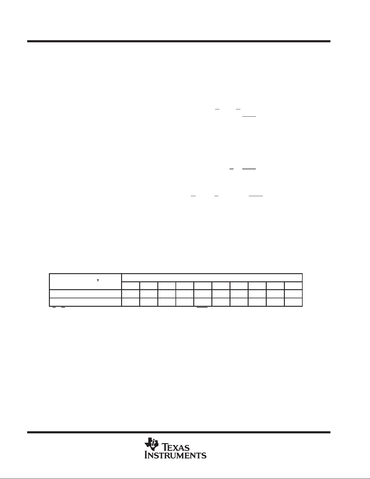
The signature mode provides access to a binary code identifying the manufacturer and type. This mode is
activated when A9 is forced to 12 V. Two identifier bytes are accessed by toggling A0. DQ0–DQ7 contain the
valid codes. All other addresses must be held low. The signature code for these devices is 97AB. A0 low selects
the manufacturer’s code 97 (Hex), and A0 high selects the device code AB (Hex), as shown in Table 3.
Table 3. Signature Mode
PINS
A0 DQ7 DQ6 DQ5 DQ4 DQ3 DQ2 DQ1 DQ0 HEX
Manufacturer Code V
Device Code V
†
E = G = VIL, A9 = VH, A1–A8 = VIL, A10–A15 = VIL, VPP = VCC, PGM = VIH or VIL.
1 0 0 1 0 1 1 1 97
IL
1 0 1 0 1 0 1 1 AB
IH
4
POST OFFICE BOX 1443 • HOUSTON, TEXAS 77251–1443
TMS27C210A 65536 BY 16-BIT UV ERASABLE
TMS27PC210A 65536 BY 16-BIT
PROGRAMMABLE READ-ONLY MEMORIES
SMLS310D– NOVEMBER 1990 – REVISED SEPTEMBER 1997
Start
Address = First Location
VCC = 6.5 V ± 0.25 V, VPP = 13 V ± 0.25 V
Program One Pulse = tw = 100 µs
Last
Address?
Yes
Address = First Location
X = 0
Increment
Address
Verify
One Byte
Pass
Fail
No
Increment Address
Program One Pulse = tw = 100 µs
No
X = 10?X = X + 1
Program
Mode
Interactive
Mode
No
VCC = VPP = 5 V ± 0.5 V
Last
Address?
Yes Yes
Compare
All Bytes
to Original
Data
Pass
Device Passed
Fail
Device Failed
Figure 1. SNAP! Pulse Programming Flowchart
Final
Verification
POST OFFICE BOX 1443 • HOUSTON, TEXAS 77251–1443
5

TMS27C210A 65536 BY 16-BIT UV ERASABLE
TMS27PC210A 65536 BY 16-BIT
PROGRAMMABLE READ-ONLY MEMORIES
SMLS310D– NOVEMBER 1990 – REVISED SEPTEMBER 1997
logic symbol
†
A0
A1
A2
A3
A4
A5
A6
A7
A8
A9
A10
A11
A12
A13
A14
A15
EPROM 65 536 × 16
21
22
23
24
25
26
27
28
29
31
32
33
34
35
36
37
2
E
0
A
65 535
15
[PWR DWN]
A ∇
A ∇
A ∇
A ∇
A ∇
A ∇
0
A ∇
A ∇
A ∇
A ∇
A ∇
A ∇
A ∇
A ∇
A ∇
A ∇
19
18
17
16
15
14
13
12
10
DQ0
DQ1
DQ2
DQ3
DQ4
DQ5
DQ6
DQ7
DQ8
9
DQ9
8
DQ10
7
DQ11
6
DQ12
5
DQ13
4
DQ14
3
DQ15
&
20
G
†
This symbol is in accordance with ANSI/IEEE Std 91–1984 and IEC Publication 617–12.
EN
6
POST OFFICE BOX 1443 • HOUSTON, TEXAS 77251–1443

VCCSuppl
oltage
V
VPPSuppl
oltage
V
VIHHigh-level dc input voltage
V
VILLow-level dc input voltage
V
TMS27C210A 65536 BY 16-BIT UV ERASABLE
TMS27PC210A 65536 BY 16-BIT
PROGRAMMABLE READ-ONLY MEMORIES
SMLS310D– NOVEMBER 1990 – REVISED SEPTEMBER 1997
absolute maximum ratings over operating free-air temperature range (unless otherwise noted)
Supply voltage range, V
Supply voltage range, V
Input voltage range (see Note 1): All inputs except A9 –0.6 V to V
(see Note 1) –0.6 V to 7 V. . . . . . . . . . . . . . . . . . . . . . . . . . . . . . . . . . . . . . . . . . . . . .
CC
–0.6 V to 14 V. . . . . . . . . . . . . . . . . . . . . . . . . . . . . . . . . . . . . . . . . . . . . . . . . . . . . . . . .
PP
CC
†
+ 1 V. . . . . . . . . . . . . . . . . . . . . . . . . . .
A9 –0.6 V to 13.5 V. . . . . . . . . . . . . . . . . . . . . . . . . . . . . . . . . . . . . . . . . . . . . . .
Output voltage range (see Note 1) –0.6 V to V
CC
+ 1 V. . . . . . . . . . . . . . . . . . . . . . . . . . . . . . . . . . . . . . . . . . . .
Operating free-air temperature range (’27C210A-_ _JL, ’27PC210A-_ _FNL) 0° C to 70°C. . . . . . . . . . . . . .
Operating free-air temperature range (’27C210A-_ _JE, ’27PC210A-_ _FNE) – 40° C to 85°C. . . . . . . . . . . .
Storage temperature range, T
†
Stresses beyond those listed under “absolute maximum ratings” may cause permanent damage to the device. These are stress ratings only, and
functional operation of the device at these or any other conditions beyond those indicated under “recommended operating conditions” is not
implied. Exposure to absolute-maximum-rated conditions for extended periods may affect device reliability.
NOTE 1: All voltage values are with respect to GND.
–65°C to 150°C. . . . . . . . . . . . . . . . . . . . . . . . . . . . . . . . . . . . . . . . . . . . . . . . . .
stg
recommended operating conditions
TMS27C/PC210A-10
TMS27C/ PC210A-12
TMS27C/ PC210A-15
TMS27C/ PC210A-20
TMS27C/ PC210A-25
MIN NOM MAX
pp
y v
pp
y v
p
p
T
Operating free-air temperature
A
T
Operating free-air temperature
A
NOTE 2: VCC must be applied before or at the same time as VPP and removed after or at the same time as VPP. The device must not be inserted
into or removed from the board when VPP or VCC is applied.
Read mode (see Note 2) 4.5 5 5.5
SNAP! Pulse programming algorithm 6.25 6.5 6.75
Read mode VCC–0.6 V
SNAP! Pulse programming algorithm 12.75 13 13.25
TTL 2 VCC+0.5
CMOS VCC– 0.2 VCC+0.5
TTL – 0.5 0.8
CMOS – 0.5 GND+0.2
’27C210A-_ _JL
’27PC210A-_ _FNL
’27C210A-_ _JE,
’27PC210A-_ _FNE
0 70 °C
–40 85 °C
CCVCC
UNIT
+0.6
POST OFFICE BOX 1443 • HOUSTON, TEXAS 77251–1443
7

TMS27C210A 65536 BY 16-BIT UV ERASABLE
VOHHigh-level dc output voltage
V
VOLLow-level dc output voltage
V
I
supply current (standby)
A
CONDITIONS
1 Seri
74
TMS27PC210A 65536 BY 16-BIT
PROGRAMMABLE READ-ONLY MEMORIES
SMLS310D– NOVEMBER 1990 – REVISED SEPTEMBER 1997
electrical characteristics over recommended ranges of operating conditions
PARAMETER TEST CONDITIONS MIN MAX UNIT
p
p
I
Input current (leakage) VI = 0 V to 5.5 V ±1 µA
I
I
Output current (leakage) VO = 0 V to V
O
I
PP1VPP
I
PP2VPP
CC1VCC
I
CC2VCC
†
Minimum cycle time = maximum address access time.
supply current VPP = VCC = 5.5 V 10 µA
supply current (during program pulse) VPP = 13 V 50 mA
pp
supply current (active)
TTL-input level VCC = 5.5 V, E = V
CMOS-input level VCC = 5.5 V, E = V
IOH = – 20 µA VCC– 0.2
IOH = – 2 mA 2.4
IOL = 2.1 mA 0.4
IOL = 20 µA 0.1
CC
IH
CC
VCC = 5.5 V, E = VIL,
t
= minimum cycle time,
cycle
outputs open
†
±1 µA
500
100
50 mA
µ
capacitance over recommended ranges of supply voltage and operating free-air
temperature, f = 1 MHz
C
I
C
O
‡
Capacitance measurements are made on a sample basis only.
§
Typical values are at TA = 25°C and nominal voltages.
Input capacitance VI = 0 V, f = 1 MHz 8 12 pF
Output capacitance VO = 0 V, f = 1 MHz 12 15 pF
‡
PARAMETER TEST CONDITIONS MIN TYP§MAX UNIT
switching characteristics over full ranges of recommended operating conditions (see Notes 3
and 4)
PARAMETER
t
t
t
t
t
¶
NOTES: 3. For all switching characteristics, the input pulse levels are 0.4 V to 2.4 V . T iming measurements are made at 2 V for logic high and
Access time from
a(A)
address
Access time from
a(E)
chip enable
Output enable
en(G)
time from G
Output disable
time from G
dis
whichever occurs
first
Output data valid
time after change
of address, E
v(A)
G
, whichever
occurs first
Value calculated from 0.5 V delta to measured level. This parameter is only sampled and not 100% tested.
4. Common test conditions apply for t
or E,
¶
, or
¶
0.8 V for logic low (see Figure 2).
TEST
CL = 100 pF,
es
TTL load,
Input tr ≤ 20 ns,
Input tf ≤ 20 ns
’27C210A-10
’27PC210A-10
MIN MAX MIN MAX MIN MAX MIN MAX MIN MAX
0 50 0 50 0 60 0 60 0 60 ns
0 0 0 0 0 ns
except during programming.
dis
’27C210A-12
’27PC210A-12
100 120 150 200 250 ns
100 120 150 200 250 ns
55 55 75 75 100 ns
’27C210A-15
’27PC210A-15
’27C210A-20
’27PC210A-20
’27C210A-25
’27PC210A-25
UNIT
8
POST OFFICE BOX 1443 • HOUSTON, TEXAS 77251–1443

TMS27C210A 65536 BY 16-BIT UV ERASABLE
TMS27PC210A 65536 BY 16-BIT
PROGRAMMABLE READ-ONLY MEMORIES
SMLS310D– NOVEMBER 1990 – REVISED SEPTEMBER 1997
switching characteristics for programming: VCC = 6.5 V and VPP = 13 V (SNAP! Pulse), TA = 25°C
(see Note 3)
PARAMETER MIN MAX UNIT
t
dis(G)
t
en(G)
NOTE 3: For all switching characteristics, the input pulse levels are 0.4 V to 2.4 V. Timing measurements are made at 2 V for logic high and
timing requirements for programming
t
w(PGM)
t
su(A)
t
su(E)
t
su(G)
t
su(D)
t
su(VPP)
t
su(VCC)
t
h(A)
t
h(D)
NOTE 3: For all switching characteristics, the input pulse levels are 0.4 V to 2.4 V. Timing measurements are made at 2 V for logic high and
Output disable time from G 0 100 ns
Output enable time from G 150 ns
0.8 V for logic low (See Figure 2).
MIN NOM MAX UNIT
Pulse duration, program SNAP! Pulse programming algorithm 95 100 105 µs
Setup time, address 2 µs
Setup time, E 2 µs
Setup time, G 2 µs
Setup time, data 2 µs
Setup time, V
Setup time, V
Hold time, address 0 µs
Hold time, data 2 µs
0.8 V for logic low (See Figure 2).
PP
CC
2 µs
2 µs
POST OFFICE BOX 1443 • HOUSTON, TEXAS 77251–1443
9

TMS27C210A 65536 BY 16-BIT UV ERASABLE
TMS27PC210A 65536 BY 16-BIT
PROGRAMMABLE READ-ONLY MEMORIES
SMLS310D– NOVEMBER 1990 – REVISED SEPTEMBER 1997
PARAMETER MEASUREMENT INFORMATION
2.08 V
Output
Under Test
RL = 800 Ω
CL = 100 pF
(see Note A)
A0–A15
DQ0–DQ15
2.4 V
0.4 V
NOTES: A. CL includes probe and fixture capacitance.
B. The ac testing inputs are driven at 2.4 V for logic high and 0.4 V for logic low. Timing
measurements are made at 2 V for logic high and 0.8 V for logic low for both inputs
and outputs.
2 V 2 V
0.8 V 0.8 V
Figure 2. The ac Testing Output Load Circuit and ac Waveform
Addresses Valid
E
t
a(E)
G
t
en(G)
t
a(A)
Hi-Z
t
v(A)
Output Valid
t
dis
Hi-Z
V
IH
V
IL
V
IH
V
IL
V
IH
V
IL
V
OH
V
OL
10
Figure 3. Read-Cycle Timing
POST OFFICE BOX 1443 • HOUSTON, TEXAS 77251–1443

PROGRAMMING INFORMATION
Program
A0–A15
t
su(A)
DQ0–DQ15
V
PP
V
CC
E
t
su(E)
PGM
G
†
t
and t
dis(G)
‡
13-V VPP and 6.5-V VCC for SNAP! Pulse programming.
are characteristics of the device but must be accommodated by the programmer.
en(G)
t
w(PGM)
Data-In Stable
t
su(D)
t
su(VPP)
t
su(VCC)
TMS27C210A 65536 BY 16-BIT UV ERASABLE
Address Stable
t
h(D)
t
TMS27PC210A 65536 BY 16-BIT
PROGRAMMABLE READ-ONLY MEMORIES
SMLS310D– NOVEMBER 1990 – REVISED SEPTEMBER 1997
Verify
V
IH
V
IL
V
/V
IH
/V
V
IL
‡
V
PP
V
CC
‡
V
CC
V
CC
V
IH
V
IL
V
IH
V
IL
V
IH
V
IL
su(G)
Data-Out
Valid
t
en(G)
Address
N + 1
t
h(A)
†
t
dis(G)
†
OH
OL
Figure 4. Program-Cycle Timing (SNAP! Pulse Programming)
POST OFFICE BOX 1443 • HOUSTON, TEXAS 77251–1443
11

TMS27C210A 65536 BY 16-BIT UV ERASABLE
TMS27PC210A 65536 BY 16-BIT
PROGRAMMABLE READ-ONLY MEMORIES
SMLS310D– NOVEMBER 1990 – REVISED SEPTEMBER 1997
FN (S-PQCC-J**) PLASTIC J-LEADED CHIP CARRIER
20 PIN SHOWN
Seating Plane
0.004 (0,10)
D
D1
13
4
E1E
8
9
NO. OF
PINS
**
D/E
19
13
18
14
MINMAXMIN
0.032 (0,81)
0.026 (0,66)
0.050 (1,27)
0.008 (0,20) NOM
D1/E1
MAX
D2/E2
MIN
0.180 (4,57) MAX
0.120 (3,05)
0.090 (2,29)
0.020 (0,51) MIN
D2/E2
D2/E2
0.021 (0,53)
0.013 (0,33)
0.007 (0,18)
MAX
M
20
28
44
52
68
84
NOTES: A. All linear dimensions are in inches (millimeters).
B. This drawing is subject to change without notice.
C. Falls within JEDEC MS-018
0.385 (9,78)
0.485 (12,32)
0.685 (17,40)
0.785 (19,94)
0.985 (25,02)
1.185 (30,10)
0.395 (10,03)
0.495 (12,57)
0.695 (17,65)
0.795 (20,19)
0.995 (25,27)
1.195 (30,35)
0.350 (8,89)
0.450 (11,43)
0.650 (16,51)
0.750 (19,05)
0.950 (24,13)
1.150 (29,21)
0.356 (9,04)
0.456 (11,58)
0.656 (16,66)
0.756 (19,20)
0.958 (24,33)
1.158 (29,41)
0.141 (3,58)
0.191 (4,85)
0.291 (7,39)
0.341 (8,66)
0.441 (11,20)
0.541 (13,74)
0.169 (4,29)
0.219 (5,56)
0.319 (8,10)
0.369 (9,37)
0.469 (11,91)
0.569 (14,45)
4040005/B 03/95
12
POST OFFICE BOX 1443 • HOUSTON, TEXAS 77251–1443

TMS27C210A 65536 BY 16-BIT UV ERASABLE
TMS27PC210A 65536 BY 16-BIT
PROGRAMMABLE READ-ONLY MEMORIES
SMLS310D– NOVEMBER 1990 – REVISED SEPTEMBER 1997
J (R-CDIP-T**) CERAMIC SIDE-BRAZE DUAL-IN-LINE PACKAGE
24 PIN SHOWN
B
24
1
0.090 (2,29)
0.060 (1,53)
0.100 (2,54)
0.065 (1,65)
0.045 (1,14)
13
12
0.018 (0,46) MIN
0.022 (0,56)
0.014 (0,36)
C
0.175 (4,45)
0.140 (3,56)
Seating Plane
0.125 (3,18) MIN
Lens Protrusion
0.010 (0,25) MAX
A
0°–10°
0.012 (0,30)
0.008 (0,20)
DIM
NOTES: A. All linear dimensions are in inches (millimeters).
PINS**
MAX
A
MIN
MAX
B
MIN
MAX
C
MIN
B. This drawing is subject to change without notice.
C. This package can be hermetically sealed with a ceramic lid using glass frit.
D. Index point is provided on cap for terminal identification only on press ceramic glass frit seal only.
NARR
0.624(15,85) 0.624(15,85)
0.590(14,99) 0.590(14,99)
1.265(32,13) 1.265(32,13)
1.235(31,37) 1.235(31,37)
0.541(13,74) 0.598(15,19)
0.514(13,06) 0.571(14,50)
24
WIDE
NARR
0.624(15,85) 0.624(15,85)
0.590(14,99) 0.590(14,99)
1.465(37,21) 1.465(37,21)
1.435(36,45) 1.435(36,45)
0.541(13,74) 0.598(15,19)
0.514(13,06) 0.571(14,50)
28
WIDE WIDE
NARR
0.624(15,85) 0.624(15,85)
0.590(14,99) 0.590(14,99)
1.668(42,37) 1.668(42,37)
1.632(41,45) 1.632(41,45)
0.541(13,74) 0.598(15,19)
0.514(13,06) 0.571(14,50)
32
WIDE
NARR
0.624(15,85) 0.624(15,85)
0.590(14,99) 0.590(14,99)
2.068(52,53) 2.068(52,53)
2.032(51,61) 2.032(51,61)
0.541(13,74) 0.598(15,19)
0.514(13,06) 0.571(14,50)
4040084/B 04/95
40
POST OFFICE BOX 1443 • HOUSTON, TEXAS 77251–1443
13

TMS27C210A 65536 BY 16-BIT UV ERASABLE
TMS27PC210A 65536 BY 16-BIT
PROGRAMMABLE READ-ONLY MEMORIES
SMLS310D– NOVEMBER 1990 – REVISED SEPTEMBER 1997
14
POST OFFICE BOX 1443 • HOUSTON, TEXAS 77251–1443

IMPORTANT NOTICE
T exas Instruments and its subsidiaries (TI) reserve the right to make changes to their products or to discontinue
any product or service without notice, and advise customers to obtain the latest version of relevant information
to verify, before placing orders, that information being relied on is current and complete. All products are sold
subject to the terms and conditions of sale supplied at the time of order acknowledgement, including those
pertaining to warranty, patent infringement, and limitation of liability.
TI warrants performance of its semiconductor products to the specifications applicable at the time of sale in
accordance with TI’s standard warranty. Testing and other quality control techniques are utilized to the extent
TI deems necessary to support this warranty . Specific testing of all parameters of each device is not necessarily
performed, except those mandated by government requirements.
CERT AIN APPLICATIONS USING SEMICONDUCTOR PRODUCTS MAY INVOLVE POTENTIAL RISKS OF
DEATH, PERSONAL INJURY, OR SEVERE PROPERTY OR ENVIRONMENTAL DAMAGE (“CRITICAL
APPLICATIONS”). TI SEMICONDUCTOR PRODUCTS ARE NOT DESIGNED, AUTHORIZED, OR
WARRANTED TO BE SUITABLE FOR USE IN LIFE-SUPPORT DEVICES OR SYSTEMS OR OTHER
CRITICAL APPLICA TIONS. INCLUSION OF TI PRODUCTS IN SUCH APPLICATIONS IS UNDERST OOD TO
BE FULLY AT THE CUSTOMER’S RISK.
In order to minimize risks associated with the customer’s applications, adequate design and operating
safeguards must be provided by the customer to minimize inherent or procedural hazards.
TI assumes no liability for applications assistance or customer product design. TI does not warrant or represent
that any license, either express or implied, is granted under any patent right, copyright, mask work right, or other
intellectual property right of TI covering or relating to any combination, machine, or process in which such
semiconductor products or services might be or are used. TI’s publication of information regarding any third
party’s products or services does not constitute TI’s approval, warranty or endorsement thereof.
Copyright 1998, Texas Instruments Incorporated
 Loading...