

TLV431Y
TLV431, TLV431A
LOW-VOLTAGE ADJUSTABLE PRECISION SHUNT REGULATORS
SLVS139C – JULY 1996 – REVISED JUL Y 1999
D
Low-Voltage Operation . . . Down to 1.24 V
D
1% Reference-V oltage Tolerance (TLV431A)
D
Adjustable Output Voltage, V
D
Low Operational Cathode Current ...80 µA Typ
D
0.25-Ω Typical Output Impedance
D
Package Options Include Plastic Small-Outline
= V
O
(D), SOT-23 (DBV), and Cylindrical (LP)
Packages
description
The TLV431 and TLV431A are low-voltage
three-terminal adjustable voltage references with
specified thermal stability over applicable
industrial and commercial temperature ranges.
Output voltage can be set to any value between
V
(1.24 V) and 6 V with two external resistors
ref
(see Figure 2). The TL V431 and TLV431A operate
from a lower voltage (1.24 V) than the widely used
TL431 and TL1431 shunt-regulator references.
When used with an optocoupler, the TLV431 and
TL V431A are ideal voltage references in isolated
feedback circuits for 3-V to 3.3-V switching-mode
power supplies. These devices have a typical
output impedance of 0.25 Ω. Active output
circuitry provides a very sharp turn-on
characteristic, making the TLV431 and TLV431A
excellent replacements for low-voltage zener
diodes in many applications, including onboard
regulation and adjustable power supplies.
ref
to 6 V
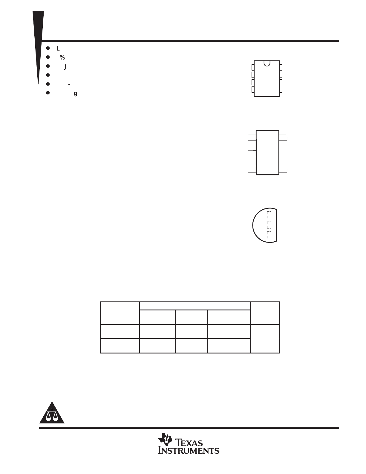
D PACKAGE
(TOP VIEW)
CATHODE
ANODE
ANODE
NC – No internal connection
NC
NC
CATHODE
NC – No internal connection
1
2
3
NC
4
DBV PACKAGE
(TOP VIEW)
1
2
3
LP PACKAGE
(TOP VIEW)
5
4
REF
8
ANODE
7
ANODE
6
NC
5
ANODE
REF
CATHODE
ANODE
REF
The TLV431C and TLV431AC devices are characterized for operation from 0°C to 70°C. The TLV431I and
TLV431AI devices are characterized for operation from –40°C to 85°C.
AVAILABLE OPTIONS
T
A
0°C to 70°C
–40°C to 85°C
The LP package is available taped and reeled. Add the suffix R to the device type
(e.g., TLV431ACLPR). The D and DBV are available only taped and reeled (e.g.,
TLV431IOR). Chip forms are tested at 25°C.
Please be aware that an important notice concerning availability, standard warranty, and use in critical applications of
Texas Instruments semiconductor products and disclaimers thereto appears at the end of this data sheet.
PRODUCTION DATA information is current as of publication date.
Products conform to specifications per the terms of Texas Instruments
standard warranty. Production processing does not necessarily include
testing of all parameters.
TO-92
(LP)
TLV431CLP
TLV431ACLP
TLV431ILP
TLV431AILP
PACKAGED DEVICES
SOIC
(D)
—
—
TLV431ID
TLV431AID
TLV431CDBV
TLV431ACDBV
TLV431AIDBV
SOT-23
(DBV)
TLV431IDBV
CHIP
FORM
(Y)
Copyright 1999, Texas Instruments Incorporated
POST OFFICE BOX 655303 • DALLAS, TEXAS 75265
1
TLV431, TLV431A
LOW-VOLTAGE ADJUSTABLE PRECISION SHUNT REGULATORS
SLVS139C – JULY 1996 – REVISED JULY 1999
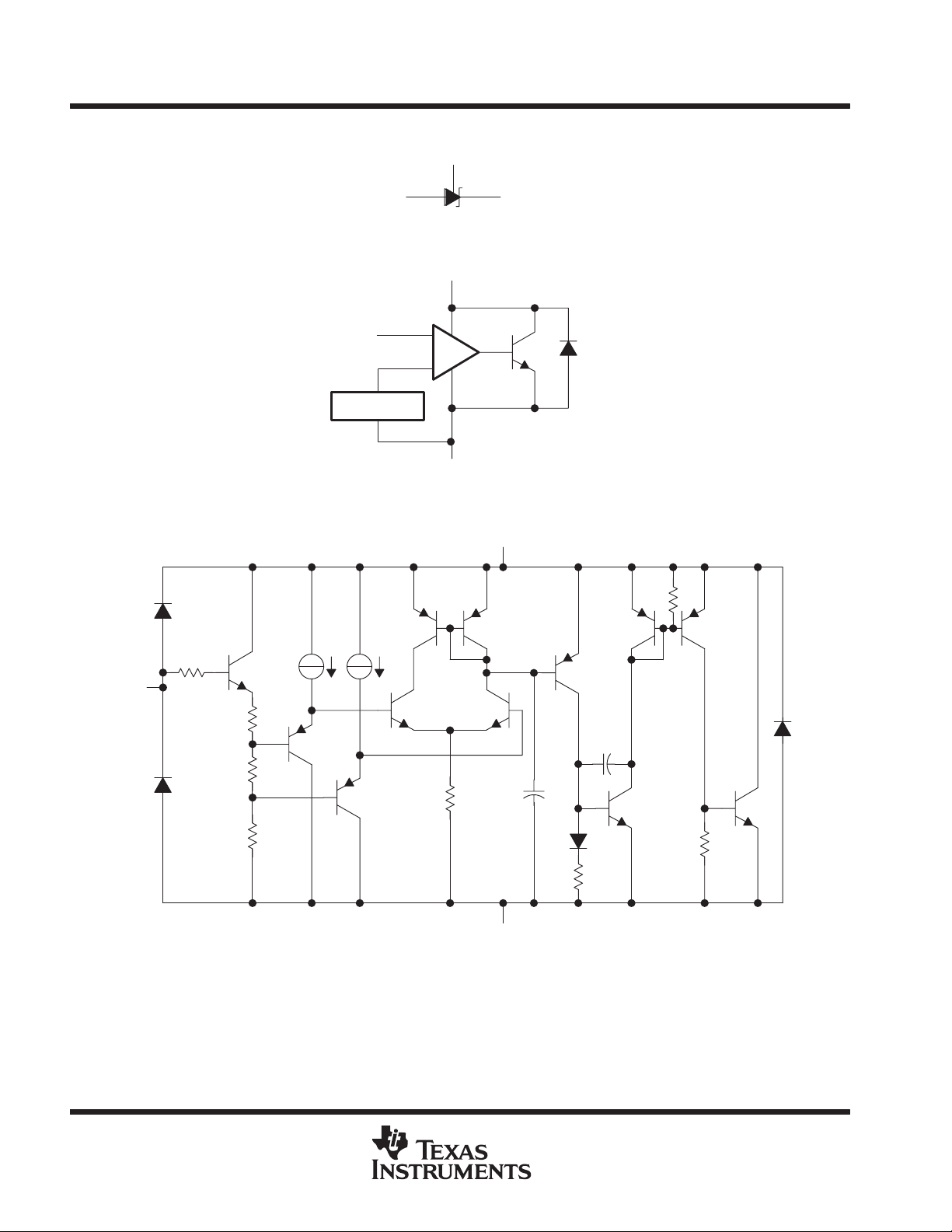
logic symbol
REF
ANODE CATHODE
logic diagram (positive logic)
CATHODE
equivalent schematic
REF
V
REF
ref
+
–
= 1.24 V
ANODE
CATHODE
ANODE
2
POST OFFICE BOX 655303 • DALLAS, TEXAS 75265
Operating free-air temperature range, T
°C
TLV431, TLV431A
LOW-VOLTAGE ADJUSTABLE PRECISION SHUNT REGULATORS
SLVS139C – JULY 1996 – REVISED JULY 1999
absolute maximum ratings over operating free-air temperature range (unless otherwise noted)
Cathode voltage, VKA (see Note 1) 7 V. . . . . . . . . . . . . . . . . . . . . . . . . . . . . . . . . . . . . . . . . . . . . . . . . . . . . . . . . . . .
Continuous cathode current range, IK –20 mA to 20 mA. . . . . . . . . . . . . . . . . . . . . . . . . . . . . . . . . . . . . . . . . . . . .
Reference current range, I
Package thermal impedance, θ
–0.05 mA to 3 mA. . . . . . . . . . . . . . . . . . . . . . . . . . . . . . . . . . . . . . . . . . . . . . . . . . . .
ref
(see Notes 2 and 3): D package 97°C/W. . . . . . . . . . . . . . . . . . . . . . . . . . . .
JA
DBV package 347°C/W. . . . . . . . . . . . . . . . . . . . . . . .
LP package 156°C/W. . . . . . . . . . . . . . . . . . . . . . . . . .
Lead temperature 1,6 mm (1/16 inch) from case for 10 seconds 260°C. . . . . . . . . . . . . . . . . . . . . . . . . . . . . . .
Storage temperature range, T
†
Stresses beyond those listed under “absolute maximum ratings” may cause permanent damage to the device. These are stress ratings only, and
functional operation of the device at these or any other conditions beyond those indicated under “recommended operating conditions” is not
implied. Exposure to absolute-maximum-rated conditions for extended periods may affect device reliability.
NOTES: 1. Voltage values are with respect to the anode terminal unless otherwise noted.
2. Maximum power dissipation is a function of TJ(max),
ambient temperature is PD = (TJ(max) – TA)/
3. The package thermal impedance is calculated in accordance with JESD 51, except for through-hole packages, which use a trace
length of zero.
–65°C to 150°C. . . . . . . . . . . . . . . . . . . . . . . . . . . . . . . . . . . . . . . . . . . . . . . . . . .
stg
θ
, and TA. The maximum allowable power dissipation at any allowable
θ
JA
JA
. Operating at the absolute maximum TJ of 150°C can impact reliability.
recommended operating conditions
MIN MAX UNIT
Cathode voltage, V
Cathode current, I
p
KA
K
p
A
TLV431C, TLV431AC 0 70
TLV431I, TLV431AI –40 85
V
ref
0.1 15 mA
6 V
°
†
POST OFFICE BOX 655303 • DALLAS, TEXAS 75265
3
TLV431, TLV431A
PARAMETER
TEST CONDITIONS
UNIT
LOW-VOLTAGE ADJUSTABLE PRECISION SHUNT REGULATORS
SLVS139C – JULY 1996 – REVISED JULY 1999
electrical characteristics at 25°C free-air temperature (unless otherwise noted)
TLV431C TLV431I
MIN TYP MAX MIN TYP MAX
TA = 25°C 1.222 1.24 1.258 1.222 1.24 1.258
V
ref
V
ref(dev)
∆V
ref
∆
V
KA
I
ref
I
ref(dev)
I
K(min)
I
K(off)
Ť
z
KA
NOTES: 4. Full range is –40°C to 85°C for the TLV431I, and 0°C to 70°C for the TLV431C.
Reference voltage
V
deviation
ref
over full temperature range
(see Note 5)
Ratio of V
in cathode voltage change
Reference terminal current
I
deviation
ref
over full temperature range
(see Note 5)
Minimum cathode current
for regulation
Off-state cathode current
Dynamic impedance
Ť
(see Note 6)
5. The deviation parameters V
over the rated temperature range. The average full-range temperature coefficient of the reference input voltage,
as:
Ť
a
where:
∆TA is the rated operating temperature range of the device.
change
ref
ppm
ǒ
Ť
V
°C
ref
ǒ
V
Ǔ
+
VKA = V
IK = 10 mA
VKA = V
(see Note 4 and Figure 1)
IK = 10 mA,
(see Figure 2)
IK = 10 mA, R1 = 10 kΩ, R2 = open
(see Figure 2)
IK = 10 mA, R1 = 10 kΩ, R2 = open
(see Note 4 and Figure 2)
VKA = V
VKA = 6 V,
(see Figure 3)
VKA = V
IK = 0.1 mA to 15 mA
(see Figure 1)
ref(dev)
V
)
ref(dev
Ǔ
at 25°C
ref
D
T
A
and I
10
6
,
ref
TA = full range
(see Note 4 and
Figure 1)
, IK = 10 mA,
ref
VKA = V
(see Figure 1) 55 80 55 80 µA
ref
V
ref
, f ≤ 1 kHz,
ref
are defined as the differences between the maximum and minimum values obtained
ref(dev)
= 0
ref
to 6 V,
1.21 1.27 1.202 1.278
4 12 6 20 mV
–1.5 –2.7 –1.5 –2.7 mV/V
0.15 0.5 0.15 0.5 µA
0.05 0.3 0.1 0.4 µA
0.001 0.1 0.001 0.1 µA
0.25 0.4 0.25 0.4 Ω
a
V
ref
V
, is defined
4
can be positive or negative, depending on whether minimum V
a
V
ref
temperature.
D
V
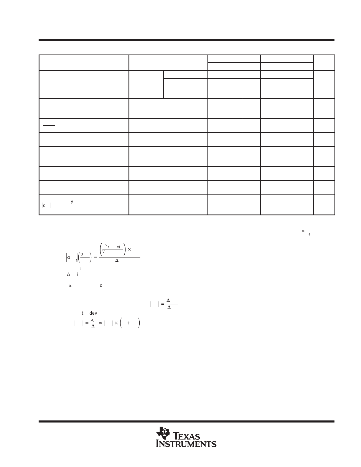
6. The dynamic impedance is defined as:
When the device is operating with two external resistors (see Figure 2), the total dynamic impedance of the circuit is given by:
D
KA
V
Ť
+
D
I
[Ťz
KA
Ť
Ť
z
ǒ1
)
R1
R2
Ť
z
KA
Ǔ
POST OFFICE BOX 655303 • DALLAS, TEXAS 75265
KA
Ť
+
D
I
KA
or maximum V
ref
, respectively, occurs at the lower
ref
PARAMETER
TEST CONDITIONS
UNIT
TLV431, TLV431A
LOW-VOLTAGE ADJUSTABLE PRECISION SHUNT REGULATORS
SLVS139C – JULY 1996 – REVISED JULY 1999
electrical characteristics at 25°C free-air temperature (unless otherwise noted)123
TLV431AC TLV431AI
MIN TYP MAX MIN TYP MAX
TA = 25°C 1.228 1.24 1.252 1.228 1.24 1.252
V
ref
V
ref(dev)
∆V
ref
∆
V
KA
I
ref
I
ref(dev)
I
K(min)
I
K(off)
Ť
z
KA
NOTES: 4. Full range is –40°C to 85°C for the TLV431I, and 0°C to 70°C for the TLV431C.
Reference voltage
V
deviation
ref
over full temperature range
(see Note 5)
Ratio of V
in cathode voltage change
Reference terminal current
I
deviation
ref
over full temperature range
(see Note 5)
Minimum cathode current
for regulation
Off-state cathode current
Dynamic impedance
Ť
(see Note 6)
5. The deviation parameters V
over the rated temperature range. The average full-range temperature coefficient of the reference input voltage,
as:
Ť
a
V
ref
where:
∆TA is the rated operating temperature range of the device.
Ť
ǒ
ppm
°C
change
ref
Ǔ
+
V
ref(dev
ǒ
V
at 25°C
ref
VKA = V
IK = 10 mA,
VKA = V
(see Note 4 and Figure 1)
IK = 10 mA,
(see Figure 2)
IK = 10 mA,
(see Figure 2)
IK = 10 mA, R1 = 10 kΩ, R2 = open
(see Note 4 and Figure 2)
VKA = V
VKA = 6 V,
(see Figure 3)
VKA = V
IK = 0.1 mA to 15 mA
(see Figure 1)
ref(dev)
)
Ǔ
10
D
T
A
and I
6
,
ref
TA = full range,
(see Note 4 and
Figure 1)
, IK = 10 mA
ref
VKA = V
R1 = 10 kΩ 0.15 0.5 0.15 0.5 µA
(see Figure 1) 55 80 55 80 µA
ref
V
ref
, f ≤ 1 kHz,
ref
are defined as the differences between the maximum and minimum values obtained
ref(dev)
= 0,
ref
to 6 V
1.221 1.259 1.215 1.265
4 12 6 20 mV
–1.5 –2.7 –1.5 –2.7
0.05 0.3 0.1 0.4 µA
0.001 0.1 0.001 0.1 µA
0.25 0.4 0.25 0.4 Ω
a
V
ref
V
mV/V
, is defined
can be positive or negative, depending on whether minimum V
a
V
ref
temperature.
D
V
6. The dynamic impedance is defined as:
When the device is operating with two external resistors (see Figure 2), the total dynamic impedance of the circuit is given by:
D
KA
V
Ť
+
D
I
[Ťz
KA
Ť
ǒ1
Ť
z
)
R1
R2
Ť
z
KA
Ǔ
POST OFFICE BOX 655303 • DALLAS, TEXAS 75265
KA
Ť
+
D
I
KA
or maximum V
ref
, respectively, occurs at the lower
ref
5

TLV431, TLV431A
PARAMETER
TEST CONDITIONS
UNIT
LOW-VOLTAGE ADJUSTABLE PRECISION SHUNT REGULATORS
SLVS139C – JULY 1996 – REVISED JULY 1999
electrical characteristics at 25°C free-air temperature12345
V
ref
∆V
ref
∆
V
KA
I
ref
I
K(min)
I
off
Ť
z
KA
NOTE 6: The dynamic impedance is defined as: Ťz
Reference voltage VKA = V
Ratio of V
in cathode voltage change
Reference terminal current IK = 10 mA, R1 = 10 kΩ, R2 = open (see Figure 2) 0.15 µA
Minimum cathode current
for regulation
Off-state cathode current VKA = 6 V, V
Dynamic impedance
Ť
(see Note 6)
When the device is operating with two external resistors (see Figure 2), the total dynamic impedance of the circuit is given by:
Ť
z
KA
Ť
+
change
ref
D
V
D
I
[Ťz
KA
Ť
ǒ1
IK = 10 mA, ∆VKA = V
VKA = V
VKA = V
(see Figure 1)
R1
Ǔ
)
R2
, IK = 10 mA (see Figure 1) TA = 25°C 1.24 V
ref
to 6 V (see Figure 2) –1.5
ref
ref
, f ≤ 1 kHz, IK = 0.1 mA to 15 mA
ref
D
V
Ť
+
KA
D
I
(see Figure 1) 55 µA
= 0 (see Figure 3) 0.001 µA
ref
KA
KA
TLV431Y
MIN TYP MAX
mV/V
0.25 Ω
PARAMETER MEASUREMENT INFORMATION
Input
I
V
ref
Figure 1. Test Circuit for V
V
= V
O
KA
= V
ref
V
O
K
= V
KA
Input
ref
,
I
Figure 2. Test Circuit for V
V
O
V
O
K(off)
= V
KA
Input
R1
R2
= V
I
ref
V
ref
× (1 + R1/R2) + I
ref
KA
I
K
> V
ref
V
O
ref
× R1
,
6
Figure 3. Test Circuit for I
POST OFFICE BOX 655303 • DALLAS, TEXAS 75265
K(off)

TLV431, TLV431A
LOW-VOLTAGE ADJUSTABLE PRECISION SHUNT REGULATORS
SLVS139C – JULY 1996 – REVISED JULY 1999
PARAMETER MEASUREMENT INFORMATION
REFERENCE VOLTAGE
vs
JUNCTION TEMPERATURE
1.254
IK = 10 mA
1.252
1.250
1.248
1.246
1.244
– Reference Voltage – V
ref
1.242
V
1.240
1.238
–50 –25 0 25 50 75 100 125 150
TJ – Junction Temperature – °C
Figure 4
†
REFERENCE INPUT CURRENT
vs
JUNCTION TEMPERATURE
250
IK = 10 mA
R1 = 10 kΩ
R2 = Open
200
150
100
– Reference Input Current – nA
ref
I
50
–50 –25 0 25 50 75 100 125 150
TJ – Junction Temperature – °C
Figure 5
CATHODE CURRENT
vs
CATHODE VOLTAGE
15
VKA = V
TA = 25°C
10
5
0
–5
– Cathode Current – mA
K
I
–10
–15
–1 –0.5 0 0.5 1 1.5
ref
VKA – Cathode Voltage – V
Figure 6
CATHODE CURRENT
vs
CATHODE VOLTAGE
250
VKA = V
TA = 25°C
200
150
Aµ
100
50
0
–50
–100
– Cathode Current –
K
I
–150
–200
–250
–1 –0.5 0 0.5 1 1.5
ref
VKA – Cathode Voltage – V
Figure 7
†
Operation of the device at these or any other conditions beyond those indicated under “recommended operating conditions” is not implied.
POST OFFICE BOX 655303 • DALLAS, TEXAS 75265
7

TLV431, TLV431A
LOW-VOLTAGE ADJUSTABLE PRECISION SHUNT REGULATORS
SLVS139C – JULY 1996 – REVISED JULY 1999
PARAMETER MEASUREMENT INFORMATION
OFF-STATE CATHODE CURRENT
vs
JUNCTION TEMPERATURE
40
VKA = 5 V
V
= 0
ref
30
20
– Off-State Cathode Current – nA
10
K(off)
I
0
–50 –25 0 25 50 75 100 125
TJ – Junction Temperature – °C
Figure 8
–0.1
–0.2
–0.3
–0.4
–0.5
– Ratio of Delta Reference Voltage
–0.6
KA
V
to Delta Cathode Voltage – mV/V
∆
/
–0.7
ref
V
∆
–0.8
†
RATIO OF DELTA REFERENCE VOLTAGE
TO DELTA CATHODE VOLTAGE
vs
JUNCTION TEMPERATURE
0
IK = 10 mA
∆VKA = V
–50 –25 0 25 50 75 100 125 150
to 6 V
ref
TJ – Junction Temperature – °C
Figure 9
PERCENTAGE CHANGE IN V
vs
OPERATING LIFE AT 55°C
0.025
IK = 1 mA
0
ref
V
– 0.025
% Change (3δ)
– 0.05
– 0.075
Percentage Change in Vref – %
– 0.1
% Change (–3δ)
– 0.125
‡
Extrapolated from life-test data taken at 125°C; the activation energy assumed is 0.7 eV.
0102030405060
Operating Life at 55°C – kh
% Change (avg)
Figure 10
ref
‡
†
Operation of the device at these or any other conditions beyond those indicated under “recommended operating conditions” is not implied.
8
POST OFFICE BOX 655303 • DALLAS, TEXAS 75265

TLV431, TLV431A
LOW-VOLTAGE ADJUSTABLE PRECISION SHUNT REGULATORS
SLVS139C – JULY 1996 – REVISED JULY 1999
PARAMETER MEASUREMENT INFORMATION
EQUIVALENT INPUT NOISE VOLTAGE
vs
nV/ Hz
350
300
250
200
VKA = V
IK = 1 mA
TA = 25°C
FREQUENCY
ref
470 µF
TLV431
or
TLV431A
3 V
1 kΩ
+
750 Ω
2200 µF
+
820 Ω
160 Ω
TLE2027
+
_
160 kΩ
TP
– Equivalent Input Noise Voltage –
n
V
150
10 100 1 k
TEST CIRCUIT FOR EQUIVALENT NOISE VOLTAGE
10 k 100 k
f– Frequency – Hz
Figure 11
POST OFFICE BOX 655303 • DALLAS, TEXAS 75265
9

TLV431, TLV431A
LOW-VOLTAGE ADJUSTABLE PRECISION SHUNT REGULATORS
SLVS139C – JULY 1996 – REVISED JULY 1999
PARAMETER MEASUREMENT INFORMATION
EQUIVALENT INPUT NOISE VOLTAGE
OVER A 10-SECOND PERIOD
10
Vµ
– Equivalent Input Noise Voltage –
n
V
f = 0.1 Hz to 10 Hz
8
IK = 1 mA
TA = 25°C
6
4
2
0
–2
–4
–6
–8
470 µF
TLV431
TLV431A
–10
0246
t – Time – s
3 V
1 kΩ
+
750 Ω
or
2200 µF
+
820 Ω
16 Ω
TEST CIRCUIT FOR 0.1-Hz TO 10-Hz EQUIVALENT NOISE VOLTAGE
TLE2027
+
_
160 kΩ
0.1 µF
10 kΩ
810
0.47 µF
10 kΩ
1 µF
33 kΩ
TLE2027
+
_
33 kΩ
2.2 µF
+
TP
CRO
1 MΩ
Figure 12
10
POST OFFICE BOX 655303 • DALLAS, TEXAS 75265

TLV431, TLV431A
LOW-VOLTAGE ADJUSTABLE PRECISION SHUNT REGULATORS
SLVS139C – JULY 1996 – REVISED JULY 1999
PARAMETER MEASUREMENT INFORMATION
SMALL-SIGNAL VOLTAGE GAIN
/PHASE MARGIN
vs
80
70
60
50
40
30
20
FREQUENCY
IK = 10 mA
TA = 25°C
0°
36°
72°
108°
144°
180°
Phase Shift
10 µF
6.8 kΩ
4.3 kΩ
Output
I
K
180 Ω
5 V
10
0
–10
– Small-Signal Voltage Gain/Phase Margin – dB
V
–20
A
1 k 10 k 100 k 1 M100
f – Frequency – Hz
REFERENCE IMPEDANCE
FREQUENCY
100
IK = 0.1 mA to 15 mA
TA = 25°C
10
1
vs
Figure 13
GND
TEST CIRCUIT FOR VOLTAGE GAIN AND PHASE MARGIN
100 Ω
Output
I
K
100 Ω
+
– Reference Impedance –
0.1
ka
|z | Ω
0.01
1 k 10 k 100 k 1 M 10 M
f – Frequency – Hz
POST OFFICE BOX 655303 • DALLAS, TEXAS 75265
–
GND
TEST CIRCUIT FOR REFERENCE IMPEDANCE
Figure 14
11

TLV431, TLV431A
LOW-VOLTAGE ADJUSTABLE PRECISION SHUNT REGULATORS
SLVS139C – JULY 1996 – REVISED JULY 1999
PARAMETER MEASUREMENT INFORMATION
3.5
3
2.5
2
1.5
1
0.5
Input and Output Voltage – V
0
–0.5
3.5
3
2.5
PULSE RESPONSE 1
Input
Output
01234
t – Time – µs
PULSE RESPONSE 2
Input
R = 18 kΩ
TA = 25°C
5678
Figure 15
R = 1.8 kΩ
TA = 25°C
18 kΩ
Pulse
Generator
f = 100 kHz
TEST CIRCUIT FOR PULSE RESPONSE 1
50 Ω
1.8 kΩ
Output
I
k
GND
Output
2
1.5
1
0.5
Input and Output Voltage – V
0
–0.5
Output
01234
t – Time – µs
5678
Figure 16
I
K
Pulse
Generator
f = 100 kHz
TEST CIRCUIT FOR PULSE RESPONSE 2
50 Ω
GND
12
POST OFFICE BOX 655303 • DALLAS, TEXAS 75265

TLV431, TLV431A
LOW-VOLTAGE ADJUSTABLE PRECISION SHUNT REGULATORS
SLVS139C – JULY 1996 – REVISED JULY 1999
PARAMETER MEASUREMENT INFORMATION
STABILITY BOUNDARY CONDITION
16
TA = 25°C
14
12
10
Stable
8
6
– Cathode Current – mA
K
4
I
2
0
0.001 0.01 0.1 1 10
150 Ω
I
K
+
C
L
–
VKA = V
VKA = 2 V
VKA = 3 V
CL – Load Capacitance – µF
V
bat
IK = 15 mA MAX
ref
C
L
Stable
R1 = 10 kΩ
‡
R2
†
150 Ω
I
K
+
V
bat
–
TEST CIRCUIT FOR VKA = V
‡
The areas under the curves represent conditions that may cause the device to oscillate. For VKA = 2-V and 3-V curves, R2 and V
adjusted to establish the initial VKA and IK conditions with CL = 0. V
ref
TEST CIRCUIT FOR VKA = 2 V, 3 V
and CL then were adjusted to determine the ranges of stability.
bat
bat
Figure 17
†
Operation of the device at these or any other conditions beyond those indicated under “recommended operating conditions” is not implied.
were
POST OFFICE BOX 655303 • DALLAS, TEXAS 75265
13

TLV431, TLV431A
LOW-VOLTAGE ADJUSTABLE PRECISION SHUNT REGULATORS
SLVS139C – JULY 1996 – REVISED JULY 1999
APPLICATION INFORMATION
Figure 18 shows the TL V431 or TLV431A used in a 3.3-V isolated flyback supply. Output voltage V
as reference voltage V
(1.24 V ±1%). The output of the regulator, plus the forward voltage drop of the optocoupler
ref
can be as low
O
LED (1.24 + 1.4 = 2.64 V), determine the minimum voltage that can be regulated in an isolated supply configuration.
Regulated voltage as low as 2.7 Vdc is possible using the circuit in Figure 18.
∼
V
120 V
I
–
P
Gate Drive
Controller
Current
GND
∼
V
CC
V
FB
Sense
+
V
O
P
P
TLV431
or
TLV431A
3.3 V
P
PP
P
Figure 18. Flyback With Isolation Using TLV431 or TLV431A as Voltage Reference and Error Amplifier
14
POST OFFICE BOX 655303 • DALLAS, TEXAS 75265

IMPORTANT NOTICE
T exas Instruments and its subsidiaries (TI) reserve the right to make changes to their products or to discontinue
any product or service without notice, and advise customers to obtain the latest version of relevant information
to verify, before placing orders, that information being relied on is current and complete. All products are sold
subject to the terms and conditions of sale supplied at the time of order acknowledgement, including those
pertaining to warranty, patent infringement, and limitation of liability.
TI warrants performance of its semiconductor products to the specifications applicable at the time of sale in
accordance with TI’s standard warranty. Testing and other quality control techniques are utilized to the extent
TI deems necessary to support this warranty . Specific testing of all parameters of each device is not necessarily
performed, except those mandated by government requirements.
CERTAIN APPLICA TIONS USING SEMICONDUCT OR PRODUCTS MAY INVOLVE POTENTIAL RISKS OF
DEATH, PERSONAL INJURY, OR SEVERE PROPERTY OR ENVIRONMENTAL DAMAGE (“CRITICAL
APPLICATIONS”). TI SEMICONDUCTOR PRODUCTS ARE NOT DESIGNED, AUTHORIZED, OR
WARRANTED TO BE SUITABLE FOR USE IN LIFE-SUPPORT DEVICES OR SYSTEMS OR OTHER
CRITICAL APPLICA TIONS. INCLUSION OF TI PRODUCTS IN SUCH APPLICATIONS IS UNDERST OOD TO
BE FULLY AT THE CUSTOMER’S RISK.
In order to minimize risks associated with the customer’s applications, adequate design and operating
safeguards must be provided by the customer to minimize inherent or procedural hazards.
TI assumes no liability for applications assistance or customer product design. TI does not warrant or represent
that any license, either express or implied, is granted under any patent right, copyright, mask work right, or other
intellectual property right of TI covering or relating to any combination, machine, or process in which such
semiconductor products or services might be or are used. TI’s publication of information regarding any third
party’s products or services does not constitute TI’s approval, warranty or endorsement thereof.
Copyright 1999, Texas Instruments Incorporated
 Loading...