

Page 1
Interfacing the TLV1562
Parallel ADĆConverter to the
TMS320C54x DSP
Application
Report
July 1999 Advanced Analog Products
SLAA040
Page 2

IMPORTANT NOTICE
T exas Instruments and its subsidiaries (TI) reserve the right to make changes to their products or to discontinue
any product or service without notice, and advise customers to obtain the latest version of relevant information
to verify, before placing orders, that information being relied on is current and complete. All products are sold
subject to the terms and conditions of sale supplied at the time of order acknowledgement, including those
pertaining to warranty, patent infringement, and limitation of liability.
TI warrants performance of its semiconductor products to the specifications applicable at the time of sale in
accordance with TI’s standard warranty. Testing and other quality control techniques are utilized to the extent
TI deems necessary to support this warranty . Specific testing of all parameters of each device is not necessarily
performed, except those mandated by government requirements.
CERTAIN APPLICATIONS USING SEMICONDUCTOR PRODUCTS MAY INVOLVE POTENTIAL RISKS OF
DEATH, PERSONAL INJURY, OR SEVERE PROPERTY OR ENVIRONMENTAL DAMAGE (“CRITICAL
APPLICATIONS”). TI SEMICONDUCTOR PRODUCTS ARE NOT DESIGNED, AUTHORIZED, OR
WARRANTED TO BE SUITABLE FOR USE IN LIFE-SUPPORT DEVICES OR SYSTEMS OR OTHER
CRITICAL APPLICA TIONS. INCLUSION OF TI PRODUCTS IN SUCH APPLICATIONS IS UNDERST OOD TO
BE FULLY AT THE CUSTOMER’S RISK.
In order to minimize risks associated with the customer’s applications, adequate design and operating
safeguards must be provided by the customer to minimize inherent or procedural hazards.
TI assumes no liability for applications assistance or customer product design. TI does not warrant or represent
that any license, either express or implied, is granted under any patent right, copyright, mask work right, or other
intellectual property right of TI covering or relating to any combination, machine, or process in which such
semiconductor products or services might be or are used. TI’s publication of information regarding any third
party’s products or services does not constitute TI’s approval, warranty or endorsement thereof.
Copyright 1999, Texas Instruments Incorporated
Page 3

Contents
1 Introduction 1. . . . . . . . . . . . . . . . . . . . . . . . . . . . . . . . . . . . . . . . . . . . . . . . . . . . . . . . . . . . . . . . . . . . . . . . . . . . . . . . . . .
2 The Board 1. . . . . . . . . . . . . . . . . . . . . . . . . . . . . . . . . . . . . . . . . . . . . . . . . . . . . . . . . . . . . . . . . . . . . . . . . . . . . . . . . . . . .
2.1 TMS320C54x Starter Kit 1. . . . . . . . . . . . . . . . . . . . . . . . . . . . . . . . . . . . . . . . . . . . . . . . . . . . . . . . . . . . . . . . . . .
2.2 TLV1562EVM 2. . . . . . . . . . . . . . . . . . . . . . . . . . . . . . . . . . . . . . . . . . . . . . . . . . . . . . . . . . . . . . . . . . . . . . . . . . . .
2.3 ADC TLV1562 Overview 2. . . . . . . . . . . . . . . . . . . . . . . . . . . . . . . . . . . . . . . . . . . . . . . . . . . . . . . . . . . . . . . . . . .
2.3.1 Suggestions for the ’C54x to TLV1562 Interface 2. . . . . . . . . . . . . . . . . . . . . . . . . . . . . . . . . . . . . . .
2.3.2 Recyclic Architecture 3. . . . . . . . . . . . . . . . . . . . . . . . . . . . . . . . . . . . . . . . . . . . . . . . . . . . . . . . . . . . . .
2.3.3 Note on the Interface, Using an External ADC Clock Drive 4. . . . . . . . . . . . . . . . . . . . . . . . . . . . . .
2.4 Onboard Components 4. . . . . . . . . . . . . . . . . . . . . . . . . . . . . . . . . . . . . . . . . . . . . . . . . . . . . . . . . . . . . . . . . . . . .
2.4.1 TLC5618 – Serial DAC 4. . . . . . . . . . . . . . . . . . . . . . . . . . . . . . . . . . . . . . . . . . . . . . . . . . . . . . . . . . . .
2.4.2 TLV5651 – Parallel DAC 5. . . . . . . . . . . . . . . . . . . . . . . . . . . . . . . . . . . . . . . . . . . . . . . . . . . . . . . . . . .
3 Operational Overview 6. . . . . . . . . . . . . . . . . . . . . . . . . . . . . . . . . . . . . . . . . . . . . . . . . . . . . . . . . . . . . . . . . . . . . . . . . .
3.1 Reference Voltage Inputs 6. . . . . . . . . . . . . . . . . . . . . . . . . . . . . . . . . . . . . . . . . . . . . . . . . . . . . . . . . . . . . . . . . .
3.2 Input Data Bits 6. . . . . . . . . . . . . . . . . . . . . . . . . . . . . . . . . . . . . . . . . . . . . . . . . . . . . . . . . . . . . . . . . . . . . . . . . . .
3.3 Connections Between the DSP and the EVM 7. . . . . . . . . . . . . . . . . . . . . . . . . . . . . . . . . . . . . . . . . . . . . . . . .
3.3.1 Jumpers Used on the TLV1562EVM 8. . . . . . . . . . . . . . . . . . . . . . . . . . . . . . . . . . . . . . . . . . . . . . . . .
4 The Serial DAC/DSP System 9. . . . . . . . . . . . . . . . . . . . . . . . . . . . . . . . . . . . . . . . . . . . . . . . . . . . . . . . . . . . . . . . . . . .
5 The DSP Serial Port 10. . . . . . . . . . . . . . . . . . . . . . . . . . . . . . . . . . . . . . . . . . . . . . . . . . . . . . . . . . . . . . . . . . . . . . . . . . .
6 Other DSP/TLV1562 Signals 11. . . . . . . . . . . . . . . . . . . . . . . . . . . . . . . . . . . . . . . . . . . . . . . . . . . . . . . . . . . . . . . . . . . .
6.1 DSP Internal Serial Port Operation 11. . . . . . . . . . . . . . . . . . . . . . . . . . . . . . . . . . . . . . . . . . . . . . . . . . . . . . . . .
7 Conversation Between the TLV1562 and the DSP 12. . . . . . . . . . . . . . . . . . . . . . . . . . . . . . . . . . . . . . . . . . . . . . . .
7.1 Writing to the ADC 12. . . . . . . . . . . . . . . . . . . . . . . . . . . . . . . . . . . . . . . . . . . . . . . . . . . . . . . . . . . . . . . . . . . . . . .
7.2 Mono Interrupt Driven Mode Using RD
7.3 Mono Interrupt Driven Mode Using CSTART
7.4 Dual Interrupt Driven Mode 15. . . . . . . . . . . . . . . . . . . . . . . . . . . . . . . . . . . . . . . . . . . . . . . . . . . . . . . . . . . . . . .
7.5 Mono Continuous Mode 16. . . . . . . . . . . . . . . . . . . . . . . . . . . . . . . . . . . . . . . . . . . . . . . . . . . . . . . . . . . . . . . . . .
7.6 Dual Continuous Mode 17. . . . . . . . . . . . . . . . . . . . . . . . . . . . . . . . . . . . . . . . . . . . . . . . . . . . . . . . . . . . . . . . . . .
8 Software Overview 18. . . . . . . . . . . . . . . . . . . . . . . . . . . . . . . . . . . . . . . . . . . . . . . . . . . . . . . . . . . . . . . . . . . . . . . . . . . .
8.1 Software Development tools 18. . . . . . . . . . . . . . . . . . . . . . . . . . . . . . . . . . . . . . . . . . . . . . . . . . . . . . . . . . . . . .
8.2 DSP Memory Map 18. . . . . . . . . . . . . . . . . . . . . . . . . . . . . . . . . . . . . . . . . . . . . . . . . . . . . . . . . . . . . . . . . . . . . . .
8.3 Programming Strategies for the ’C54x, Explanations 20. . . . . . . . . . . . . . . . . . . . . . . . . . . . . . . . . . . . . . . . .
8.3.1 Optimizing CPU Resources for Maximum Data Rates 20. . . . . . . . . . . . . . . . . . . . . . . . . . . . . . . . .
8.3.2 Address and Data Bus for I/O Tasks 20. . . . . . . . . . . . . . . . . . . . . . . . . . . . . . . . . . . . . . . . . . . . . . . .
8.3.3 Timer Output 20. . . . . . . . . . . . . . . . . . . . . . . . . . . . . . . . . . . . . . . . . . . . . . . . . . . . . . . . . . . . . . . . . . . .
8.3.4 Data Page Pointer 21. . . . . . . . . . . . . . . . . . . . . . . . . . . . . . . . . . . . . . . . . . . . . . . . . . . . . . . . . . . . . . .
8.3.5 Generating the Chip Select Signal and the CSTART
8.3.6 Interfacing the Serial DAC 5618 to the DSP 21. . . . . . . . . . . . . . . . . . . . . . . . . . . . . . . . . . . . . . . . .
8.3.7 Interrupt Latency 22. . . . . . . . . . . . . . . . . . . . . . . . . . . . . . . . . . . . . . . . . . . . . . . . . . . . . . . . . . . . . . . . .
8.3.8 Branch Optimization (goto/dgoto, call/dcall, ...) 22. . . . . . . . . . . . . . . . . . . . . . . . . . . . . . . . . . . . . . .
8.3.9 Enabling Software Modules (.if/.elseif/.endif) 23. . . . . . . . . . . . . . . . . . . . . . . . . . . . . . . . . . . . . . . . .
8.4 Software Code Explanation 23. . . . . . . . . . . . . . . . . . . . . . . . . . . . . . . . . . . . . . . . . . . . . . . . . . . . . . . . . . . . . . .
8.4.1 Software Principals of the Interface 23. . . . . . . . . . . . . . . . . . . . . . . . . . . . . . . . . . . . . . . . . . . . . . . . .
8.5 Flow Charts and Comments for All Software Modes 27. . . . . . . . . . . . . . . . . . . . . . . . . . . . . . . . . . . . . . . . . .
8.5.1 The Mono Interrupt Driven Mode Using RD
8.5.2 Mono Interrupt Driven Mode Using CSTART
8.5.3 Dual Interrupt Driven Mode 33. . . . . . . . . . . . . . . . . . . . . . . . . . . . . . . . . . . . . . . . . . . . . . . . . . . . . . . .
8.5.4 Mono Continuous Mode 36. . . . . . . . . . . . . . . . . . . . . . . . . . . . . . . . . . . . . . . . . . . . . . . . . . . . . . . . . .
to Start Conversion 27. . . . . . . . . . . . . . . . . . . . . . . .
to Start Conversion 30. . . . . . . . . . . . . . . . . . . . . . .
Signal 21. . . . . . . . . . . . . . . . . . . . . . . . . . . .
12. . . . . . . . . . . . . . . . . . . . . . . . . . . . . . . . . . . . . . . . . . . . . . . . . . . . .
14. . . . . . . . . . . . . . . . . . . . . . . . . . . . . . . . . . . . . . . . . . . . . . . .
Interfacing the TLV1562 Parallel AD-Converter to the TMS320C54x DSP
iii
Page 4

Contents
8.5.5 Dual Continuous Mode 38. . . . . . . . . . . . . . . . . . . . . . . . . . . . . . . . . . . . . . . . . . . . . . . . . . . . . . . . . . .
8.5.6 C-Callable With Mono Interrupt Driven Mode Using CSTART
to Start Conversion 40. . . . . . . . .
8.6 Source Code 41. . . . . . . . . . . . . . . . . . . . . . . . . . . . . . . . . . . . . . . . . . . . . . . . . . . . . . . . . . . . . . . . . . . . . . . . . . . .
8.6.1 Common Software for all Modes (except C-Callable) 41. . . . . . . . . . . . . . . . . . . . . . . . . . . . . . . . .
8.6.2 Mono Mode Interrupt Driven Software Using RD
to Start Conversion 46. . . . . . . . . . . . . . . . . . . .
8.6.3 Calibration of the ADC 53. . . . . . . . . . . . . . . . . . . . . . . . . . . . . . . . . . . . . . . . . . . . . . . . . . . . . . . . . . . .
8.6.4 Mono Mode Interrupt Driven Software Using CSTART
to Start Conversion 58. . . . . . . . . . . . . . .
8.6.5 Dual Interrupt Driven Mode 66. . . . . . . . . . . . . . . . . . . . . . . . . . . . . . . . . . . . . . . . . . . . . . . . . . . . . . . .
8.6.6 Mono Continuous Mode 74. . . . . . . . . . . . . . . . . . . . . . . . . . . . . . . . . . . . . . . . . . . . . . . . . . . . . . . . . .
8.6.7 Dual Continuous Mode 80. . . . . . . . . . . . . . . . . . . . . . . . . . . . . . . . . . . . . . . . . . . . . . . . . . . . . . . . . . .
8.6.8 C-Callable 86. . . . . . . . . . . . . . . . . . . . . . . . . . . . . . . . . . . . . . . . . . . . . . . . . . . . . . . . . . . . . . . . . . . . . .
9 Summary 93. . . . . . . . . . . . . . . . . . . . . . . . . . . . . . . . . . . . . . . . . . . . . . . . . . . . . . . . . . . . . . . . . . . . . . . . . . . . . . . . . . . . .
10 References 93. . . . . . . . . . . . . . . . . . . . . . . . . . . . . . . . . . . . . . . . . . . . . . . . . . . . . . . . . . . . . . . . . . . . . . . . . . . . . . . . . .
iv
SLAA040
Page 5

Figures
List of Figures
1 TLV1562 – DSP Interface of the EVM, Using RD or the CSTART Signal to Start Conversion 2. . . . . . . . . . . . . . .
2 TLV1562 – DSP Interface of the EVM, Using RD
3 TLC5618 – DSP Interface 5. . . . . . . . . . . . . . . . . . . . . . . . . . . . . . . . . . . . . . . . . . . . . . . . . . . . . . . . . . . . . . . . . . . . . . . . .
4 TLC5651 – DSP Interface 5. . . . . . . . . . . . . . . . . . . . . . . . . . . . . . . . . . . . . . . . . . . . . . . . . . . . . . . . . . . . . . . . . . . . . . . . .
5 Memory Map 19. . . . . . . . . . . . . . . . . . . . . . . . . . . . . . . . . . . . . . . . . . . . . . . . . . . . . . . . . . . . . . . . . . . . . . . . . . . . . . . . . . .
6 Software Flow of the Mono Interrupt Driven Solution 29. . . . . . . . . . . . . . . . . . . . . . . . . . . . . . . . . . . . . . . . . . . . . . . .
7 Flow Chart Mono Interrupt Driven Mode Using CSTART
8 Time Optimization (monocst1) Maximum Performance at 12 MSPS with Internal Clock 33. . . . . . . . . . . . . . . . . . .
9 Flow Chart Dual Interrupt Driven Mode (Using CSTART
10 Flow Chart Mono Continuous Mode 37. . . . . . . . . . . . . . . . . . . . . . . . . . . . . . . . . . . . . . . . . . . . . . . . . . . . . . . . . . . . . .
11 Flow Chart Dual Continuous Mode 39. . . . . . . . . . . . . . . . . . . . . . . . . . . . . . . . . . . . . . . . . . . . . . . . . . . . . . . . . . . . . . .
or the CSTART Signal to Start Conversion 3. . . . . . . . . . . . . . .
to Start Conversion 31. . . . . . . . . . . . . . . . . . . . . . . . . . . .
) to Start Conversion 35. . . . . . . . . . . . . . . . . . . . . . . . . . .
List of Tables
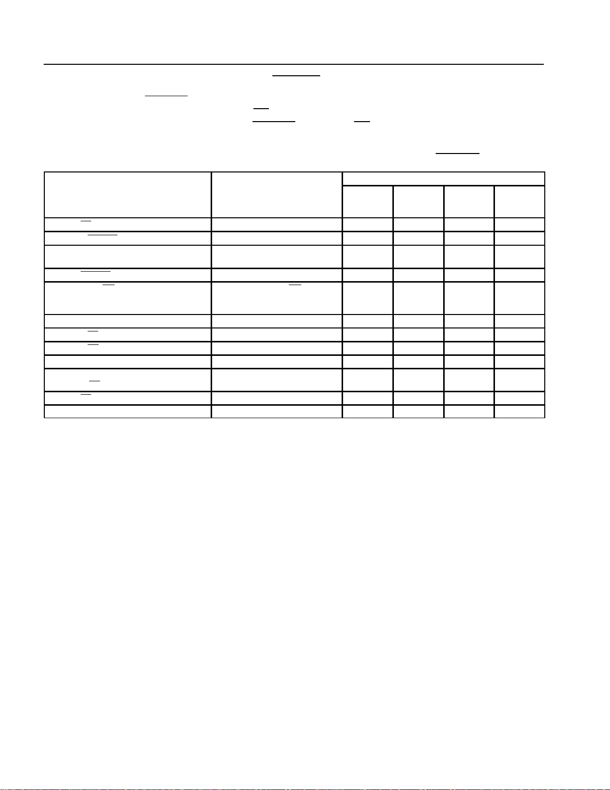
1 Signal Connections 7. . . . . . . . . . . . . . . . . . . . . . . . . . . . . . . . . . . . . . . . . . . . . . . . . . . . . . . . . . . . . . . . . . . . . . . . . . . . . . .
2 3-Position Jumpers 8. . . . . . . . . . . . . . . . . . . . . . . . . . . . . . . . . . . . . . . . . . . . . . . . . . . . . . . . . . . . . . . . . . . . . . . . . . . . . . .
3 2-Position Jumpers 8. . . . . . . . . . . . . . . . . . . . . . . . . . . . . . . . . . . . . . . . . . . . . . . . . . . . . . . . . . . . . . . . . . . . . . . . . . . . . . .
4 DSP/DAC Interconnection 9. . . . . . . . . . . . . . . . . . . . . . . . . . . . . . . . . . . . . . . . . . . . . . . . . . . . . . . . . . . . . . . . . . . . . . . . .
5 DSP Serial Port Signals and Registers 10. . . . . . . . . . . . . . . . . . . . . . . . . . . . . . . . . . . . . . . . . . . . . . . . . . . . . . . . . . . . .
6 DSP Algorithm for Writing to the ADC 12. . . . . . . . . . . . . . . . . . . . . . . . . . . . . . . . . . . . . . . . . . . . . . . . . . . . . . . . . . . . . .
7 DSP Algorithm for Mono Interrupt Driven Mode Using RD
8 DSP Algorithm for Mono Interrupt Driven Mode Using CSTART
9 DSP Algorithm for Dual Interrupt Driven Mode 15. . . . . . . . . . . . . . . . . . . . . . . . . . . . . . . . . . . . . . . . . . . . . . . . . . . . . .
10 DSP Algorithm for Mono Continuous Mode 16. . . . . . . . . . . . . . . . . . . . . . . . . . . . . . . . . . . . . . . . . . . . . . . . . . . . . . . .
11 DSP Algorithm for Dual Continuous Mode 17. . . . . . . . . . . . . . . . . . . . . . . . . . . . . . . . . . . . . . . . . . . . . . . . . . . . . . . . .
12 Switch Settings 26. . . . . . . . . . . . . . . . . . . . . . . . . . . . . . . . . . . . . . . . . . . . . . . . . . . . . . . . . . . . . . . . . . . . . . . . . . . . . . . .
13 Instruction in the Program Header (Step 1) 26. . . . . . . . . . . . . . . . . . . . . . . . . . . . . . . . . . . . . . . . . . . . . . . . . . . . . . . .
14 Instruction in the Program Header (Step 1) 27. . . . . . . . . . . . . . . . . . . . . . . . . . . . . . . . . . . . . . . . . . . . . . . . . . . . . . . .
13. . . . . . . . . . . . . . . . . . . . . . . . . . . . . . . . . . . . . . . . . . . .
14. . . . . . . . . . . . . . . . . . . . . . . . . . . . . . . . . . . . . . .
Interfacing the TLV1562 Parallel AD-Converter to the TMS320C54x DSP
v
Page 6

vi
SLAA040
Page 7

Interfacing the TLV1562 Parallel ADC to the TMS320C54x DSP
Falk Alicke and Perry Miller
ABSTRACT
In this application report we discuss the hardware and software interface of the TL V1562,
10-bit parallel-output analog-to-digital converter (ADC) to the TMS320C54x digital signal
processor (DSP).
consists of the TLV1562 10-bit ADC, a THS5651 10-bit parallel output
communication digital-to-analog converter (CommsDAC) and a TLC5618A
serial-output digital-to-analog converter (DAC).
Following the discussion of the ADC we explain the need for both the THS5651
CommsDAC and the TLC5618A serial DAC.
The application report concludes with several software application examples and
recommendations for simplifying the software through modifications of the DSP
hardware interface circuit.
1 Introduction
The analog-to-digital (A/D) interface can present a significant design problem
because hardware and software must work together across the interface to
produce a usable, complete design. This application report provides a design
solution for the interface between the TLV1562 10-bit parallel-output
analog-to-digital converter (ADC) and the TMS320C54x digital signal processor
(DSP).
The report describes the hardware and software needed to interface the ’C54x
DSP to the TL V1562 ADC, which is intended for applications, such as industrial
control and signal intelligence in which large amounts of data must be processed
quickly. The first sections describe the basic operation of the TLV1562. For
additional information see the References section at the end of this report.
The hardware interface board, or evaluation module (EVM)
2 The Board
The TL V1562 evaluation module (EVM) is a four-layer printed circuit board (PCB)
constructed from FR4 material. The PCB dimensions are 180 mm × 112 mm ×
12 mm. Ribbon cables are used to interface the TLV1562EVM to the
TMS320C54x DSK plus starter kit.
2.1 TMS320C54x Starter Kit
The starter kit simplifies the task of interfacing to the ’C54x processor. It comes
with an ADC for voice bandwidth, and GoDSP code explorer as the software tool.
A 10-MHz oscillator provides the clock signal to allow 40-MHz internal DSP clock
cycles generated by the internal DSP PLL. Therefore, the board provides 40
MIPS of processing power.
Ribbon cables are used to connect the DSP with the EVM. Detailed descriptions
of all connections are given later in this report.
CommsDAC is a trademark of Texas Instruments.
1
Page 8
The Board
2.2 TLV1562EVM
The TLV1562EVM gives customers an easy start with employing many of the
features of this converter. A serial DAC (TLC5618A), a parallel DAC (THS5651),
and the ADC (TL V1562) make this EVM flexible enough to test the features of the
TLV1562. It also helps show how this ADC can be implemented.
2.3 ADC TLV1562 Overview
The TL V1562 is a CMOS 10-bit high-speed programmable resolution analog-todigital converter, using a low-power recyclic architecture.
The converter provides two differential or four single-ended inputs to interface the
analog input signals.
On the digital side, the device has a chip-select (CS
sample/conversion start signal (CSTART
input (WR
), and 10 parallel data I/O lines (D9:0).
The converter integrates the CSTART
), read signal input (RD), write signal
signal to coordinate sampling and
conversion timing without using the parallel bus. Since the TMS320C542 DSP
has no second general-purpose output, this signal is generated with the signal
(CSTART
) from the address decoder.
2.3.1 Suggestions for the ’C54x to TLV1562 Interface
The following paragraphs describe two suggested interfaces between the ’C54x
and the TLV1562.
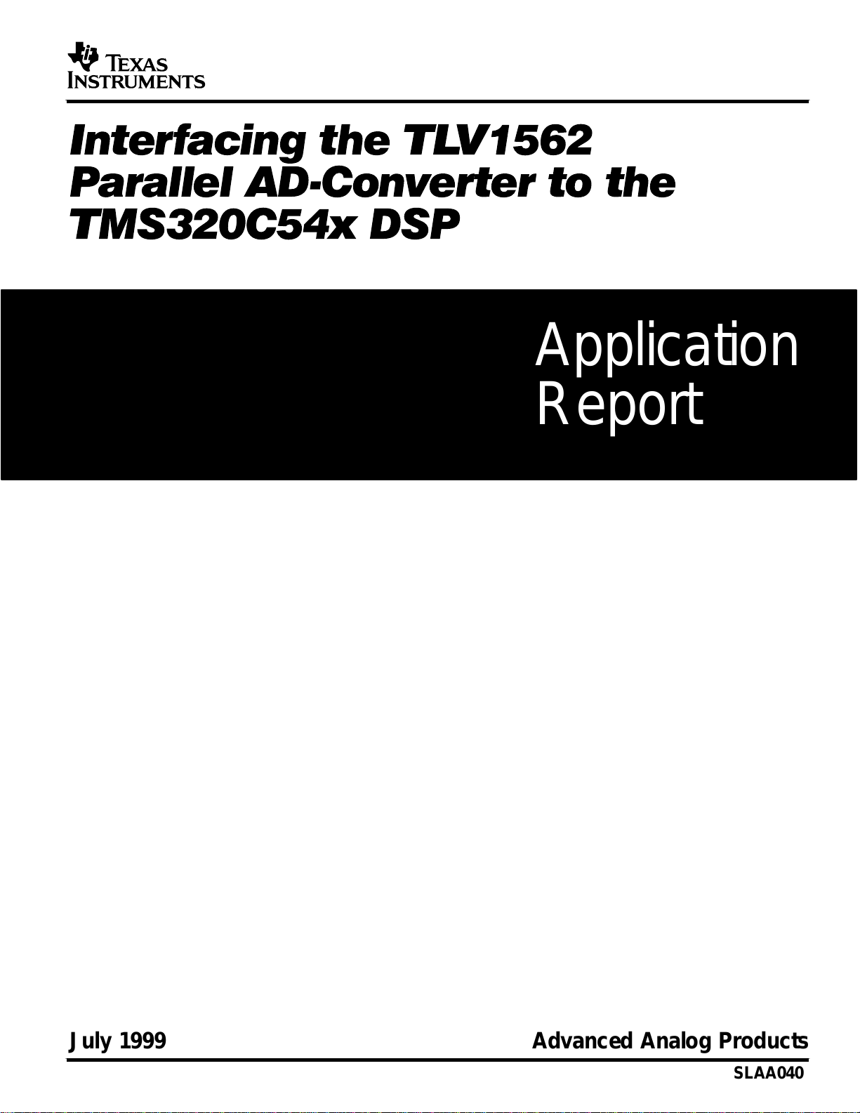
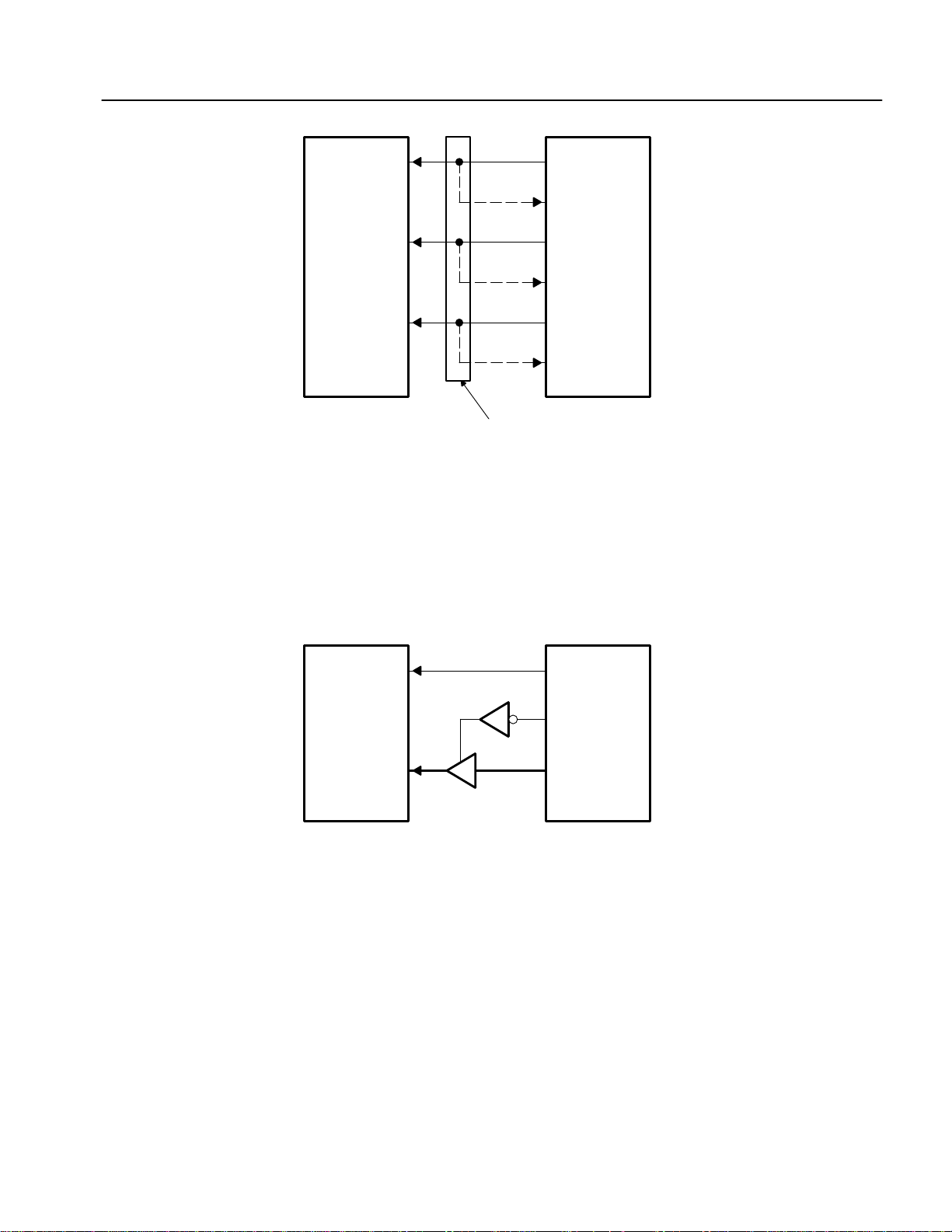
2.3.1.1 The Universal Interface
The schematic in Figure 1 shows the pin-to-pin connections between the
TL V1562 and ’C54x, realized on the EVM. This routing can test the converter in
each mode. One I/O-wait state is required for write operations to the ADC. The
read sequence from the ADC does not require any wait states because the RD
signal is generated with XF.
TLV1562 TMS320C54x
INT
CSTART
CS
01
10
11
Address
Decoder
), input clock (CLKIN),
INT
A0
A1
2 SLAA040
RD
WR
CLKIN
D(0–9) D(0–9)
≥ 1
1: x
Divider
XF
IOSTRB
R/W
CLOCKOUT
Figure 1. TLV1562 to ’C54x DSP Interface of the EVM,
Using RD or the CSTART Signal to Start Conversion
Page 9
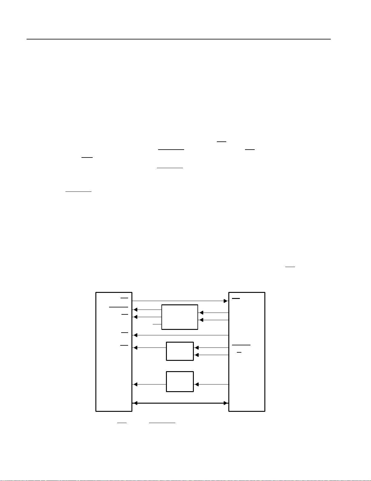
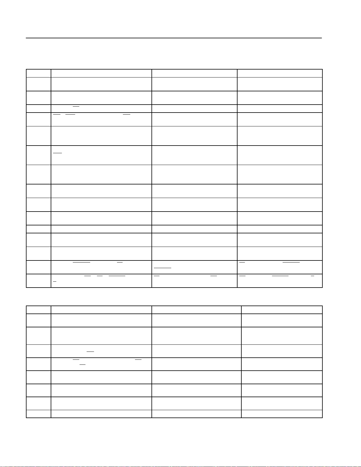
2.3.1.2 Simplification of Software Requirements Through Modified Interface
Of all the TL V1562 modes of operation, only the mono interrupt driven mode uses
the RD
signal to start the conversion. This requires a very flexible handling of the
read signal and therefore has to be performed by a general-purpose output
signal. If the application excludes using the RD
(using CSTART
instead). The TLV1562 RD input signal can be generated with
an OR gate, whose inputs are driven by IOSTRB
signal to start the conversion
and R/W signals from the DSP
(see Figure 2).
Using these connections saves the programming steps of setting/resetting RD
with the XF signal. Another advantage is having XF available to control the
CSTART
signal. This saves busy times on the address bus (in Figure 1, CST ART
was generated through A0/A1.) and simplifies the software code.
CAUTION:
The time t
EN(DATAOUT)
between the RD high-to-low transition
(generated by the DSP) and the arrival of valid ADC output
data on the data bus is related to the capacitive load of the
bus. In most cases, the ADC come out of the 3-state mode
and supplies the correct voltage levels onto the bus lines in
less than 50 ns. Thus, the minimum number of I/O-wait states
becomes two (for t
TLV1562 TMS320C54x
INT
CSTART
CS
EN(DATAOUT)
01
10
11
≤50 ns).
Address
Decoder
INT
XF
A0
A1
The Board
CLKIN
D(0–9) D(0–9)
Figure 2. TLV1562 to ’C54x DSP Interface of the EVM,
Using RD
2.3.2 Recyclic Architecture
One specialty of this ADC is its recyclic architecture. Instead of limiting the device
power by the highest possible resolution at the fastest speed, this converter is
able to work at three maximum speeds for three resolutions. The highest
resolution runs at 2MSPS maximum throughput rate; 8-bit resolution
corresponds to 3MSPS, and 4-bit resolution to 7MSPS.
RD
WR
≥ 1
&
≥ 1
1: x
Divider
IOSTRB
R/W
CLOCKOUT
or the CSTART Signal to Start Conversion
Interfacing the TLV1562 Parallel ADC to the TMS320C54x DSP
3
Page 10
The Board
This feature fits well into monitoring application. For example, the ADC may have
to trigger on one event out of some channels inside an extremely small time
window and then sample the correct channel with a higher resolution, but lower
throughput to analyze this process. This feature also fits well into home security
applications or applications that must monitor several inputs simultaneously.
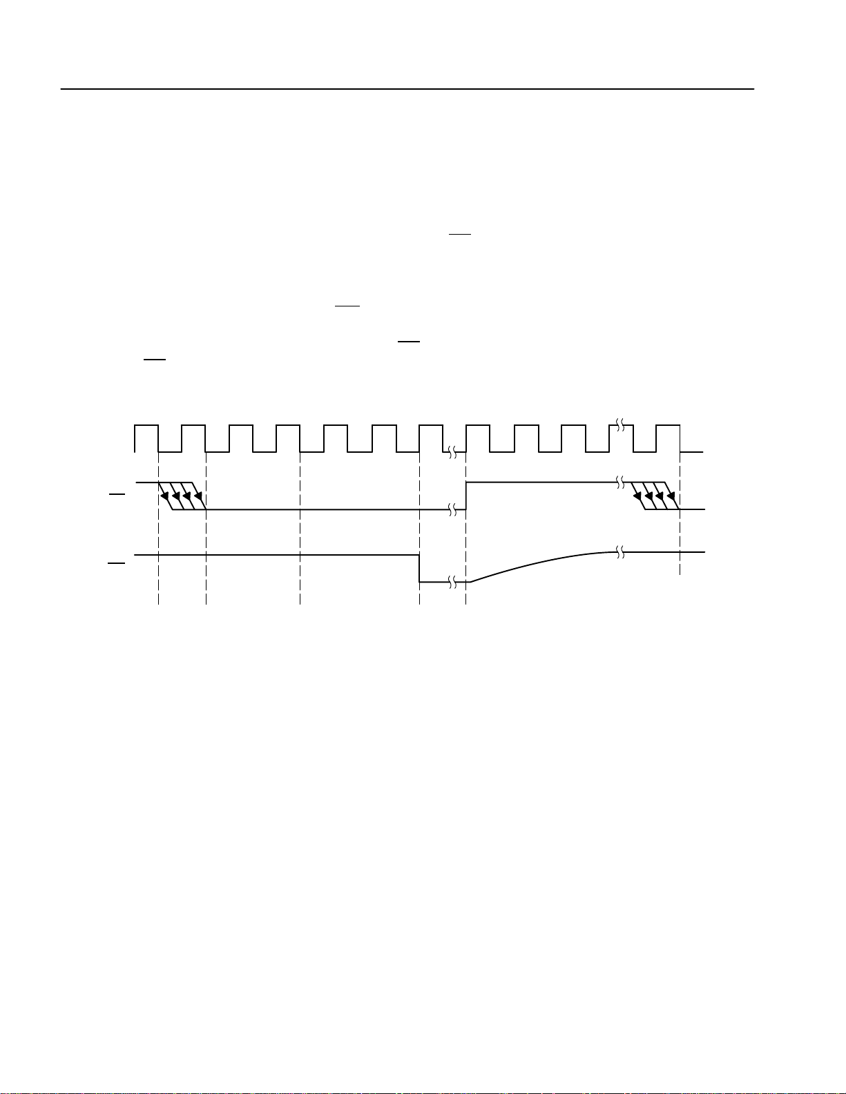
2.3.3 Note on the Interface, Using an External ADC Clock Drive
The TL V1562data sheet (Figure 9) shows that RD has to fall as close as possible
to the falling edge of the clock signal. The user must adhere to this timing,
otherwise the conversion result may be wrong. The user may not recognize the
erroneous result, since the ADC will signal that the conversion has finished during
the logic low transition of the INT
interface behavior of the ADC whether the timing is correct or not. The following
figure shows what happens when the RD
RD
falls nearly 1/2 of one cycle too late, the conversion result is valid on the 5
clock cycle.
signal. The following timing diagram shows the
falling edge is timed wrong. Although
th
12345678910
CLK
RD
INT
Conversion Starts
Next Sampling Starts
2.4 Onboard Components
These sections describe the EVM onboard components.
2.4.1 TLC5618A – Serial DAC
This 12-bit DAC has a serial interface that can run at 20-MHz clock; therefore, it
can update the output at 1.21 MSPS. Two outputs are available on the 8-pin
package. The buffered SPI of the DSP provides the DSP interface. Using the
auto-buffer mode, updating the data on the DAC requires only four CPU
instructions/samples.
1
Conversion Finished
4 SLAA040
Page 11
The Board
Serial DAC
SCLK
CS
TLC5618A
DIN
TLV1562 EVM Pin Connector
Figure 3. TLC5618A to ’C542 DSP Interface
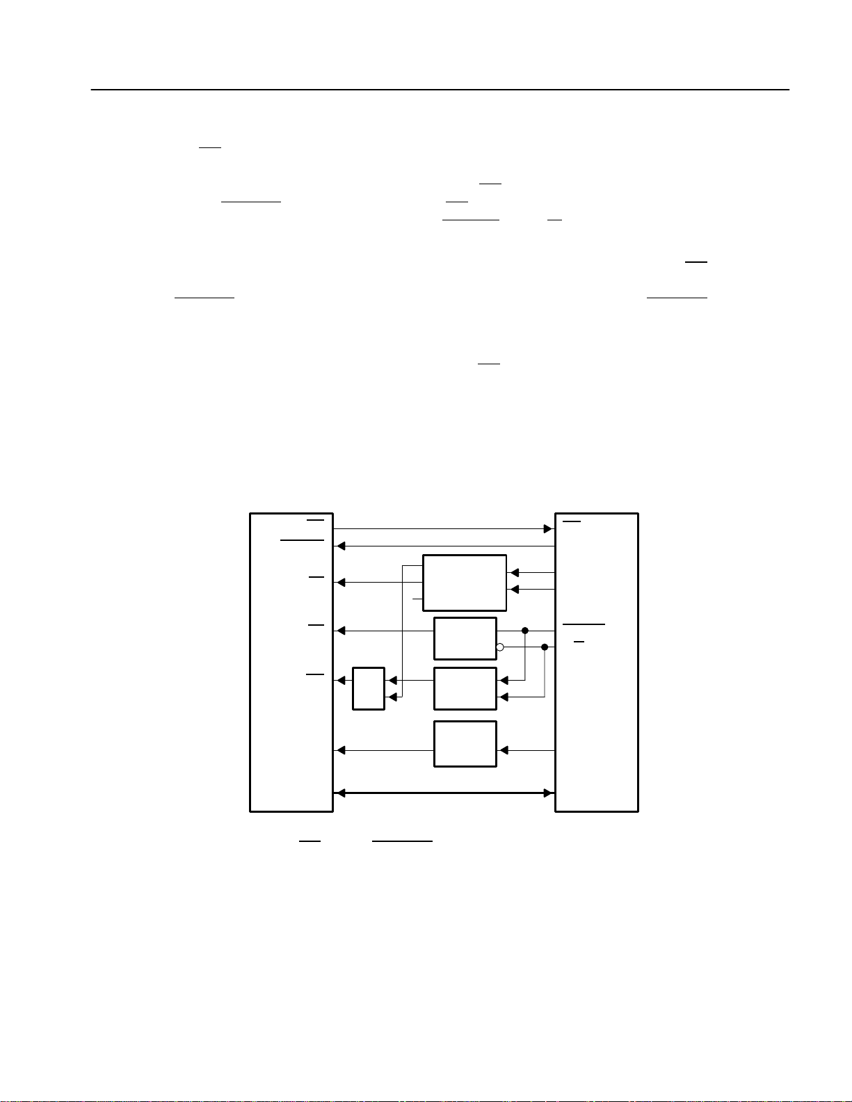
2.4.2 THS5651 – Parallel Output CommsDAC
This 10-bit data converter has a parallel interface and is able to update its output
with 100 MSPS. The two outputs on the 28-pin package can each drive a current
between 2 mA and 20 mA with an output resistance >100 kΩ (ideal current
source: output impedance → ∞). The data bus and the address decoder provide
the interface to the DSP.
Parallel DAC
DSP
BCLKX
BCLKR
BFSX
TMS320C542
BFSR
BDX
BDR
DSP
CLK
THS5651
D(0–9)
Buffer
CLKOUT
TMS320C542
A(0–1) = 11
D(0–9)
b
Figure 4. THS5651 to C542 DSP Interface
Interfacing the TLV1562 Parallel ADC to the TMS320C54x DSP
5
Page 12

Operational Overview
3 Operational Overview
This chapter discusses the software and hardware interface for the TLV1562.
Plus the overall operational sequence of the A/D interface is described.
3.1 Reference Voltage Inputs
The voltage difference between the VREFP and VREFM terminals determines
the analog input range, i.e., the upper and lower limits of the analog inputs that
produce the full-scale (output data all 1s) and zero-scale (output data all 0s)
readings, respectively.
For design reasons, this high-speed sampling ADC does not have a groundreferenced input voltage range. Hence, level shifting is required unless the
application allows the signal to be ac coupled. Level shifting could be done with
single-supply op amps.
The absolute voltage values applied to VREFP, VREFM, and the analog input
should not be greater than the A V
input restrictions apply so consult the TL V1562 data sheet for further information.
The digital output is full scale when the analog input is equal to or greater than
the voltage on VREFP , and is zero scale when the input signal is equal to or lower
than VREFM.
supply minus 1 V , or lower than 0.8 V . Other
DD
3.2 Input Data Bits
The ADC contains the two user-accessible registers, CR0 and CR1. All user
defined features such as conversion mode, data output format or sample size are
programmed in CR0 and CR1. The data acquisition process must be started by
writing to these two registers. After this initialization, the converter processes
data in the same configuration until these registers are overwritten.
6 SLAA040
Page 13

3.3 Connections Between the DSP and the EVM
The following connections provide the interface between the DSP and the EVM:
Table 1. Signal Connections
Operational Overview
DSP Signal Connector/Pin on the DSKplus cir-
cuit board
General
GND Connector JP4: Pin 1, 10, 1 1, 12, 14,
15, 19, 20, 21, 27, 34, 35
Connector JP5: Pin 6, 10, 1 1, 12
VCC JP1/32 N/A VCC
Parallel Interface
CLKOUT JP3/2 J11/11 CLKIN
INT0
XF JP4/8 J11/3 RD
R/W JP4/30 J11/9 decoded to the WR line
IOSTRB JP4/36 J11/7 decoded to the WR line
A0 JP5/34 J11/2 addr. decoder for CS and CSTART
A1 JP5/35 J11/1 addr. decoder for CS and CSTART
D0 JP3/35 J10/13 D0
D1 JP3/34 J10/15 D1
D2 JP3/8 J10/17 D2
D3 JP3/12 J10/19 D3
D4 JP3/11 J10/21 D4
D5 JP3/15 J10/23 D5
D6 JP3/14 J10/25 D6
D7 JP3/18 J10/27 D7
D8 JP3/17 J10/29 D8
D9 JP3/21 J10/31 D9
Serial Interface to the DAC TLC5618A
BCLKR JP1/14 J11/25 SCLK
BCLKX JP1/17 J11/23 SCLK
BFSR JP1/20 J11/21 CS
BFSX JP1/23 J11/19 CS
BDR JP1/26 J11/17 DIN
BDX JP1/29 J11/15 DIN
JP5/1 J11/5 INT
Connector/Pin on
the TLV1562EVM
J10/2,J10/4,...,J10/34
J11/4,J11/6,...,J11/26
ADC Signal
GND
Signals D[9–0] of the TLV1562 and D[9–0] of the DSP are tied together in this
application to simplify hardware debugging during the development phase.
However, if the 2s complement feature of the DAC is to be used, it is easier to
connect D[15-6] of the DSP with D[9–0] of the ADC. A simple right shift of the
result then evaluates the result when sign extension mode (SXM) is enabled.
Interfacing the TLV1562 Parallel ADC to the TMS320C54x DSP
7
Page 14
Operational Overview
3.3.1 Jumpers Used on the TLV1562EVM
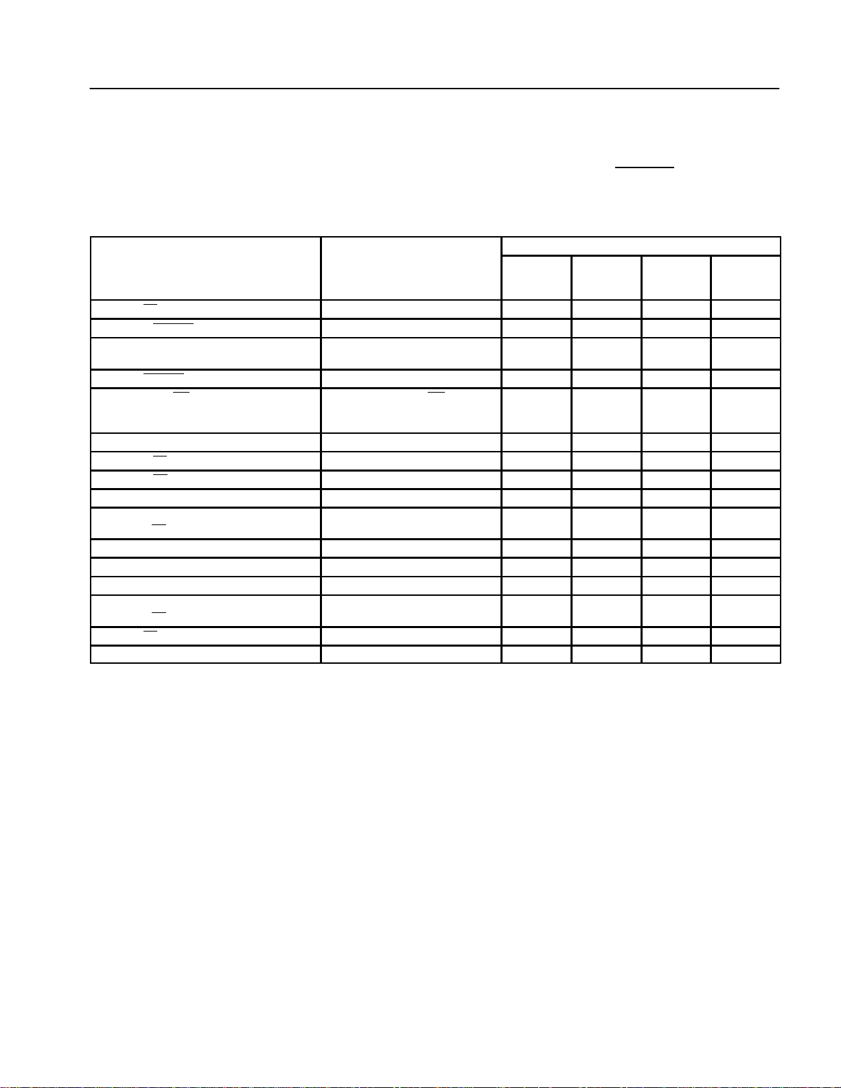
Table 2. 3-Position Jumpers
JUMPER GENERAL DESCRIPTION PIN 1-2 PIN 2-3
W1 Connects BP/CH3 (ADC) to R45 or GND; Input not in use, grounded to reduce noise Use as single input channel3 or
W2 Connects BM/CH4 (ADC) to R44 or GND; Input not in use, grounded to reduce noise Use as single input channel4 or
W3 Connects RD to XF or /RD1 Logic generator is connected to the ADC DSP is connected to the ADC
W4 WR + WR1 is connected with DSP_WR or
W5
W6
W7
W8 MCB_CLK is connected to BUFCLK (U14) or
W9 CLK input of the Counter (U2) is connected with
W10 ADC CLKIN is connected to CLK/2 or CLK/4 The ADC clock runs at a quarter of the
W11 Connects AP/CH1 (ADC) to R48 or GND; Input not in use, grounded to reduce
W12 Connects AM/CH2 (ADC) to R47 or GND; Input not in use, grounded to reduce
W13 Connects REFLO (TL V5651) to Vcc or GND Disable internal reference Enable internal reference
W14 Connects SCLK (TLC5618AA) to BCLKX or J8
W15 Connects CLK (TLV5651) to CLKOUT (DSP) or
W23 Connects CSTAR T to A0, A1, or XF A0 and A1 used to generate ADC
W24 Connects DSP_RD to XF or IOSTRB, ORed with
U12-J9/3
The three Jumpers define the prescaling of the
CLKOUT signal to the MCB_CLK Pin, if W8 is
set to Counter-Mode
(U11)
RD1
CLKOUT or CLKOUT/2
(BNC)
J7 (BNC)
/W from the DSP
R
Logic generator is connected to the ADC DSP is connected to the ADC
Counter-Mode (MCB_CLK signal is
divided by the counter, set-up with
Jumper W(5-7)
The counter is toggled by the DSP
system clock (signal BUFF_CLK)
DSP clock frequency (10 MHz)
noise
noise
Normal DSP mode An external clock source drives the
Normal DSP mode An external clock source drives the CLK
signal
CSTART
XF signal connected to ADC RD pin RD pin driven by IOSTRB ORed with R/W
differential input positive channel B
differential input negative channel B
Counter-Mode disabled (MCB_CLK is
synchronize with the CLKOUT signal)
The counter’s clock is prescaled by two
(toggled by half the DSP system clock
(CLKOUT2))
The ADC clock runs at half the DSP
clock frequency (20 MHz)
Use as single input channel 1 or
differential input positive channel A
Use as single input channel 2 or
differential input negative channel A
SCLK pin instead of the DSP
pin instead of the DSP
XF signal connects to CSTAR T pin
Table 3. 2-Position Jumpers
JUMPER GENERAL DESCRIPTION PINS SHORTED PINS OPEN
W16 Connects Mode input (TLV 5651) to GND MODE 0 is chosen (binary data input) MODE 1 is chosen (2s complement
W17 Connects REFIO (TLV5651) to VREF1 or leaves
the REFIO pin decoupled to GND via a 0.1 µF
capacitor
W18 Connects DIR (U19) to GND or leaves the DIR
pin connected to WR
W19 Connects OE (U19) to GND or leaves the OE pin
connected to CS
W20 Connects BDX to BDR or leaves BDR open DSP BDR pin gets a shortcuted feedback
W21 Connects BSFX to BSFR or leaves BCLKR open DSP BSFR pin gets a shortcuted feedback
W22 Connects BCLKX backwards with BCLKR or
leaves it open
W28 Connect Sleep input (TLV5651/5 GND Normal mode of operation Sleep mode seleted
Use as external reference voltage input Use as internal reference voltage
ADC can only write but not read to the data
bus
Output driver is isolated and disabled (no
signal can bus trough the data bus)
from the BDX (transmit) pin; normal mode
from the BSFX (transmit) pin; normal mode
DSP BCLKR pin gets a shortcuted feedback
from the BCLKX (transmit) pin; normal mode
8 SLAA040
data input)
output with this pin terminated into
GND in series with 0.1 pF
Normal operation mode
Normal operation mode
BDR remains open
BSFR remains open
BCLKR remains open
Page 15
4 The Serial DAC/DSP System
The software configures the buffered DSP serial port to the 16-bit master mode
so that the DSP generates the frame sync signal at BFSX and the data clock at
BCLKX serial port terminals. Table 4 shows the connections between the DSP
and the DAC TLC5618A.
Table 4. DSP/DAC Interconnection
FROM DSP TO DSP TO DAC
BFSX BFSR CS
BCLKX CLKR I/O CLK
BDX BDR DATA IN
The following statements describe the generation and application of the
configuration and control signals.
• The DSP BCLKX output provides a 20-MHz data clock, which is a divide-by-2
of the DSP master clock.
• The DSP BDX output supplies the 16-bit control and data move to the
TLC5618A at DATA IN.
• The DSP BFSX frame synchronization signal, connected to CS, triggers the
start of a new frame of data.
The Serial DAC/DSP System
After the falling edge of FSX, the next 16 data clocks transfer data into the DSP
DR terminal and out of the DX terminal. Since this DSP/DAC interface is
synchronous, the FSX signal is sent to the FSR terminal, and the CLKX is sent
to the CLKR terminal.
Interfacing the TLV1562 Parallel ADC to the TMS320C54x DSP
9
Page 16

The DSP Serial Port
5 The DSP Serial Port
The buffered serial port provides direct communication with serial I/O devices and
consists of six basic signals and five registers. The DSP internal serial port
operation section discusses the registers.
The six signals are:
• BCLKX - The serial transmit clock. This signal clocks the transmitted data
from the BDX terminal to the DIN terminal of the TLC5618A.
• BCLKR - The serial receive clock. This signal clocks data into the DSP BDR
terminal. Since the DAC does not send any information back to the DSP, this
signal is not important.
• BDX - Data transmit. From this terminal the DSP transmits 16-bit data to the
DIN terminal of the TLC5618A.
• BDR - Data receive – not in use
• BFSX - Frame sync transmit. This signal frames the transmit data. The DSP
begins to transmit data from BDX on the falling edge of BFSX and continues
to transmit data for the next 16 clock cycles from the BCLKX terminal. The
BFSX signal is applied to the TLC5618A CS
• BFSR - Frame sync receive. This signal frames the receive data. The DSP
begins to receive data on the falling edge of BFSR and continues to recognize
valid data for the following 16 clocks from BCLKR. This signal is not important
for this application.
terminal.
Table 5 lists the serial port pins and registers.
Table 5. DSP Serial Port Signals and Registers
PINS DESCRIPTION REGISTERS DESCRIPTION
BCLKX Transmit clock signal BSPC Serial port control register
BCLKR Receive clock signal BSPCE extended BSPC
BDX Transmitted serial data signal BDXR Data transmit register
BDR Received serial data signal BDRR Data receive register
BFSX Transmit frame synchronization signal BXSR Transmit shift register
BFSR Receive frame synchronization signal BRSR Receive shift register
AXR Buffer start location
BKX Buffer size
For this application the DSP buffered serial port is programmed as the master,
so the BCLKX output is fed to the BCLKR terminal and the BFSX output is fed to
the BFSR terminal.
10 SLAA040
Page 17

6 Other DSP/TLV1562 Signals
These paragraphs describe other DSP and TLV1562 signals.
6.1 DSP Internal Serial Port Operation
Three signals are necessary to connect the transmit pins of the transmitting
device with the receive pins of the receiving device for data transmission. The
transmitted serial data signal (BDX) sends the actual data. BFSX initiates the
transfer (at the beginning of the packet), and BCLKX clocks the bit transfer. The
corresponding pins on the receive device are BDR, BFSR and BCLKR,
respectively.
The transmit is executed by the autobuffer mode. This means there is no need
to write to the serial port output buffer . Instead, the DSP continuously sends the
data, located in the memory beginning on AXR. When all data are sent (defined
by the buffer length in BXR), the first word (pointed to by AXR) is sent again.
Therefore, the program has only to store the samples into this memory location.
The rest of the task is handled in the background, using no CPU power.
Other DSP/TLV1562 Signals
Interfacing the TLV1562 Parallel ADC to the TMS320C54x DSP
11
Page 18

Conversation Between the TLV1562 and the DSP
7 Conversation Between the TLV1562 and the DSP
The complexity of the TLV1562 ADC may be confusing because of the number
of possible modes to drive the protocol between DSP and ADC. The following
paragraphs explain more about the data sheet descriptions for interfacing the
’C54x to the ADC.
7.1 Writing to the ADC
Registers CR0 and CR1 must be set to choose any of the modes the TLV1562
offers. Therefore, a write sequence must be performed from the DSP to the ADC.
After selecting the ADC (CS
low), a high-low transition of the WR line tells the
converter that something is to be written to the data port.
Table 6. DSP Algorithm for Writing to the ADC
STEPS TIMING, NOTES
1. Set one DSP I/O waitstate Make timing between 40 MHz C54x CPU compatible with the TLV1562
2. Clear CS Select ADC
3. Send out data on the bus The signal WR is automatically handled by the DSP
4. Set CS Deselect ADC
7.2 Mono Interrupt Driven Mode Using RD
This mode is used when the application needs to sample one channel at a time
and performs the sampling, conversion, and serial transmission steps only once.
Although this mode produces continuous sampling data, the use of other modes
is recommended. One reason is the CS
sampling/conversion time. An interesting advantage of this mode is its ability to
control the start-sample time.
The RD
stops the sampling process (disconnects the capacitor from the input signal) and
starts the signal conversion. After two ADCSYSSCLKs, the sampling capacitor
gets connected back to the input signal to do the next sampling. The conversion
time needs five ADCSYSCLKs to finish the conversion before it gets written to the
data port.
signal controls the sampling and converting. Every falling edge of RD
signal has to stay low during the whole
During configuration, the rising edge of WR
Also, when conversion is finished, the ADC clears the INT signal purposes. Next
the ADC writes the conversion result to the data port. The rising edge of RD
this status; in other words, the INT
conversion result on the data port becomes invalid (the ADC data port gets
3-stated).
The configuration data needs to be written only once to the ADC. After this,
toggling the RD
the RD
12 SLAA040
starts the sampling.
resets
signal goes back to logic high and the
signal runs the ADC in a sampling/conversion/sending mode and
signal releases every new cycle.
Page 19
Table 7. DSP Algorithm for Mono Interrupt Driven Mode Using RD
STEPS TIMING, NOTES
0. Initialization
Write all configuration data to the
ADC
1. set CS deselect ADC (optional with APD=0)
2. clear CS Select ADC
3. Wait for
t
D(CSL-sample)
+1ADCSYSCLK
activate the mono interrupt-driven mode
in CR0(2;3)
(Note: if Hardware Auto power down is
enabled, Chip select has to be used,
otherwise CS can be left high)
t
D(CSL-sample)
t
D(CSL-sample)
= 5ns (APD=0)
= 500ns (APD=1)
Conversation Between the TLV1562 and the DSP
Wait cycles for the DSP internally (40 MHz DSPCLK):
APD=0
ADCSYCLK
= 7.5 MHz
≥6 ≥5 ≥26 ≥25
APD=0
ADCSYCLK
= 10 MHz
APD=1
ADCSYCLK
= 10 MHz
APD=1
ADCSYCLK
= 10 MHz
4. Clear RD ADC goes over from sampling into
conversion
5. Wait until INT goes low alternative: ignore the INT signal, wait 49
ns+5(6) ADCSYSCLK and goto step
number 7
6. Wait the time t
EN(DATAOUT)
t
EN(DATAOUT)
= 41 ns ≥2 ≥2 ≥2 ≥2
7. Read sample out from the data port;
Reset RD
signal
8. Goto step 1 or step 3 (if APD=0) for
more samples
≥34 ≥22 ≥34 ≥22
Interfacing the TLV1562 Parallel ADC to the TMS320C54x DSP
13
Page 20
Conversation Between the TLV1562 and the DSP
7.3 Mono Interrupt Driven Mode Using CSTART
Use the CSTART signal when two or more ADCs must sample/convert signals
at the same time. Instead of the RD
is started with the edges of the CST ART
get the data out of the ADC and onto the bus.
Table 8. DSP Algorithm for Mono Interrupt Driven Mode Using CSTART
STEPS TIMING, NOTES
1. Set CS Deselect ADC
2. Clear CSTART tTis starts sampling
3. Wait for t
4. Set CSTART This starts the conversion
5. Wait until INT goes low Alternative: ignore the INT signal,
6. Wait the time t
7. Clear CS Select the ADC
8. Clear RD Start communication
9. Wait the time t
10. Read sample out from the data port;
Reset RD
11. Set CS Deselect ADC
12. Go to step 2 for the next samples
W(CSTARTL)
D(INTL-CSI)
EN(DATAOUT)
signal
t
W(CSTARTL)
t
W(CSTARTL)
wait 14ns+5 ADCSYSCLK and goto
step number 7
t
D(INTL-CSI)
t
EN(DATAOUT)
signal, the timing for sampling and converting
signal. The RD signal is still required to
= 100 ns (APD=0)
= 600 ns (APD=1)
= 10 ns ≥1 ≥1 ≥1 ≥1
= 41 ns ≥2 ≥2 ≥2 ≥2
Wait cycles for the DSP internally (40MHz DSPCLK):
APD=0
ADCSYCLK
= 7.5 MHz
≥4 ≥4 ≥24 ≥24
≥33 ≥21 ≥33 ≥21
APD=0
ADCSYCLK
= 10 MHz
APD=1
ADCSYCLK
= 10 MHz
APD=1
ADCSYCLK
= 10 MHz
14 SLAA040
Page 21
7.4 Dual Interrupt Driven Mode
Using techniques similar to those described in the first two modes for
sampling/converting/sending tasks, the dual mode samples two channels at the
same time and sends out the results in series to the data port. The CST AR T
is used to start sampling and converting.
Table 9. DSP Algorithm for Dual Interrupt Driven Mode
STEPS TIMING, NOTES
1. Set CS Deselect ADC
2. Clear CSTART This starts sampling
3. Wait for t
4. Set CSTART This starts the conversion
5. Wait until INT goes low Alternative: ignore the INT signal,
6. Wait the time t
7. Clear CS Select the ADC
8. Clear RD Start communication
9. Wait the time t
10. Read sample out from the data port;
reset RD
11. Wait t
12. Clear RD- Start communication
13. Wait the time t
14. Read sample out from the data port;
reset RD
15. Set CS Deselect ADC
16. Goto step 2 for the next samples
W(CSTARTL)
D(INTL-CSL)
EN(DATAOUT)
signal
W(CSH)
EN(DATAOUT)
signal
t
W(CSTARTL)
t
W(CSTARTL)
wait 210ns+10 ADCSYSCLK and go
to step number 7
t
D(INTL-CSI)
t
EN(DATAOUT)
t
W(CSH)
t
EN(DATAOUT)
= 100ns (APD=0)
= 600ns (APD=1)
= 10 ns ≥1 ≥1 ≥1 ≥1
= 41 ns ≥2 ≥2 ≥2 ≥2
= 50 ns ≥2 ≥2 ≥2 ≥2
= 41 ns ≥2 ≥2 ≥2 ≥2
Conversation Between the TLV1562 and the DSP
pin
Wait cycles for the DSP internally (40MHz DSPCLK):
APD=0
ADCSYCLK
= 7.5MHz
≥4 ≥4 ≥24 ≥24
≥62 ≥48 ≥62 ≥48
APD=0
ADCSYCLK
= 10MHz
APD=1
ADCSYCLK
= 10MHz
APD=1
ADCSYCLK
= 10MHz
Interfacing the TLV1562 Parallel ADC to the TMS320C54x DSP
15
Page 22
Conversation Between the TLV1562 and the DSP
7.5 Mono Continuous Mode
This mode simplifies data acquisition, since there is no need to generate a signal
to sample or convert data. Instead, initializing this mode once, the ADC sends out
the data continuously and will be read by the DSP with the RD
CAUTION:
In this mode, the sampling result sent out by the ADC is the
value of the sample from the last cycle. Therefore, the first
sample after initialization is trash.
Table 10. DSP Algorithm for Mono Continuous Mode
Wait cycles for the DSP internally (40MHz DSPCLK):
STEPS TIMING, NOTES
0. Initialization N/A N/A
Write all configuration data to the
ADC
1. Set CS Deselect ADC N/A N/A
2. wait for t
3. Clear CS Select ADC N/A N/A
4. Clear RD Start conversion N/A N/A
5. Wait the time t
6. Read sample out from the data port;
reset RD
7. Wait for the time t
step 7 and 8 to ensure 5(6) ADCSYSCLk
8. Go to step 4 for more samples N/A N/A
(SAMPLE1)
EN(DATAOUT)
signal
(CONV1)
minus
Activate the mono continuous mode in
CR0(2;3)
t
(SAMPLE1)
t
EN(DATAOUT)
(Caution: the first result after initialization
is trash)
t
(CONV1)
7 and 8 take at least 4 DSPSYSCLK, the
calculation are 5(6) ADCSYSCLK minus
100 ns
= 100 ns ≥4 ≥4 N/A N/A
= 41 ns ≥2 ≥2 N/A N/A
= 5(6) ADCSYSCLK; since step
APD=0
ADCSYCLK
= 7.5 MHz
≥23 ≥16 N/A N/A
signal.
APD=0
ADCSYCLK
= 10 MHz
APD=1
ADCSYCLK
= 10 MHz
N/A N/A
N/A N/A
APD=1
ADCSYCLK
= 10 MHz
16 SLAA040
Page 23

Conversation Between the TLV1562 and the DSP
7.6 Dual Continuous Mode
The dual continuous mode provides a data stream of two input signals. The
characteristic of the data protocol is similar to the mono continuous mode but with
the use of two RD
In this mode, the sampling result sent out by the ADC is the
value of the sample from the last cycle. Therefore, the first
sample after initialization is trash.
Table 11. DSP Algorithm for Dual Continuous Mode
STEPS TIMING, NOTES
0. Initialization N/A N/A
Write all configuration data to the
ADC
1. Set CS deselect ADC N/A N/A
2. Wait for t
3. Clear CS Select ADC N/A N/A
4. Clear RD Start conversion
5. Wait the time t
6. Read first sample out from the
data port; reset RD
7. Wait for the time t
step 7 and 8 to ensure 5(6) ADCSYSCLk
8. Clear RD Start conversion
9. Wait the time t
10. Read second sample out from the
data port; reset RD
11. Wait for the time t
step 7 and 8 to ensure 5(6) ADCSYSCLk
12. Go to step 4 for more samples N/A N/A
(SAMPLE1)
EN(DATAOUT)
EN(DATAOUT)
signal
(CONV1)
signal
(CONV1)
minus
minus
cycles for one sample/hold cycle.
CAUTION:
Wait cycles for the DSP internally (40MHz DSPCLK):
ADCSYCLK
Activate the dual continuous mode in
CR0(2;3)
t
(SAMPLE1)
t
EN(DATAOUT)
(Caution: the first result after initialization
is trash)
t
(CONV1)
and 8 take at least 4 DSPSYSCLK, the
calculation are 5(6)ADCSYSCLK minus
100 ns
t
EN(DATAOUT)
(Caution: the first result after initialization
is trash)
t
(CONV1)
and 8 take at least 4 DSPSYSCLK, the
calculation are 5(6)ADCSYSCLK minus
100ns
= 100 ns ≥4 ≥4 N/A N/A
= 41 ns ≥2 ≥2 N/A N/A
= 5(6) ADCSysclk; since step 7
= 41 ns ≥2 ≥2 N/A N/A
= 5(6) ADCSysclk; since step 7
APD=0
= 7.5 MHz
≥23 ≥16 N/A N/A
≥23 ≥16 N/A N/A
APD=0
ADCSYCLK
= 10 MHz
APD=1
ADCSYCLK
= 10 MHz
N/A N/A
N/A N/A
N/A N/A
APD=1
ADCSYCLK
= 10 MHz
Interfacing the TLV1562 Parallel ADC to the TMS320C54x DSP
17
Page 24

Software Overview
8 Software Overview
The software in this report shows how to use all modes of the TL V1562 and useful
variations for each mode. It also includes a C program to start data acquisition
from a C level. To limit the number of programs, the report supplies five files for
running the ADC in five modes; a sixth program shows the C-callable function.
Each program can enable different software blocks to give the user a large choice
for generating the data acquisition. For more details, see paragraph 8.3.9.
Instead of using numbers for memory addresses or constants, very often
symbols replace the numbers. For that, the symbol (name) is assigned with the
real value (number) in the file header. The advantage of doing this is the higher
flexibility. Instead of changing a variable memory location in every related
instruction, the value for this location is changed only once in the program header.
This prevents software bugs from appearing through a forgotten correction of a
related instruction.
BSPC_BUFFER_START set 00800h ; memory location (800h) for the
@AXR = #(BSPC_BUFFER_START) ; assign the starting address of auto
8.1 Software Development tools
The DSKplus Starter Kit of the TMS320C54x comes with a free compiler to
generate an absolute object file from assembler code (DSKPLASM.EXE in the
TMS320C54x DSKplus development tools). The object code is then loaded into
the GoDSP software to run it on the kit.
An advanced version of this kit is the TMS320C54x Optimizing C Compiler/
Assembler/Linker (for example: TMDS324L855-02). These tools allow
generation of object code from C and assembler files. Furthermore, they also link
the code to an executable COFF file. The software in this report was created with
these tools.
For more information visit TI’s Internet page at:
http://www.ti.com/sc/docs/dsps/tools/c5000/c54x/index.htm
8.2 DSP Memory Map
Figure 6 shows the memory map assigned to the application.
PROGRAM MEMORY (on-chip DARAM 10k words (OVLY=1) from 0080h to 27FFh):
; start address of the SPC buffer
; buffer
.
18 SLAA040
Page 25
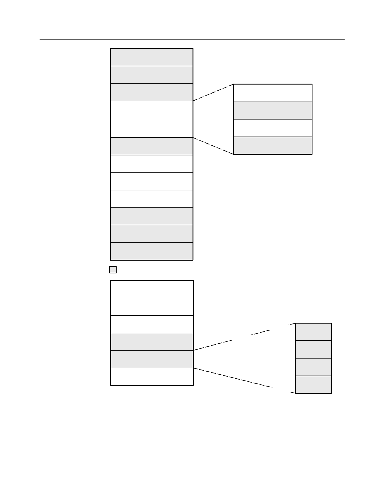
0000h
007Fh
0080h
00FFh
0100h
017Fh
0180h
07FFh
0800h
0FFFh
1000h
1009h
100Ah
17FFh
1800h
27FFh
2800h
EFFFh
F000h
F7FFh
F800h
FF7Fh
FF80h
FFFFh
(OVLY = 1)
Original Interrupts DSKplus
Starter Kit
Communication Kernel
Starter Kit
RAM
BSP RAM Block or Program RAM
Kernel Buffer (10 Words)
HPI RAM Block or Porgram RAM
Program
External
On-Chip ROM
ROM (Bootloader)
ROM Interrupts
01FFh
0200h
027Fh
0280h
02FFh
0300h
Software Overview
Unused
Software Interrupt Table
Unused
Linked Program Memory Code
0000h
005Fh
0060h
007Fh
0080h
27FFh
1800h
1FFFh
2000h
27FFh
2800h
FFFFh
Reserved Memory by The DSKplus Board
Memory-Mapped Register
Scratch-Pad RAM
DRAM See Program Memory
Software Data Memory
(All Variables)
Tables to Store Data Samples
External
Figure 5. Memory Map
Interfacing the TLV1562 Parallel ADC to the TMS320C54x DSP
data_log_A
data_loc_A + num_data_A
data_loc_B
data_loc_B + num_data_B
data_loc_C
data_loc_C + num_data_C
data_loc_D
data_loc_D + num_data_D
Table 1
Table 2
Table 3
Table 4
19
Page 26

Software Overview
8.3 Programming Strategies for the ’C54x, Explanations
Before listing the program code, this chapter introduces some basic instructions
(strategies) to provide the ’C54x user with some ideas for dealing with the DSP
architecture.
8.3.1 Optimizing CPU Resources for Maximum Data Rates
The ’C54x processor on the DSKplus starter kit runs at an internal clock
frequency of 40 MHz. Since the pipeline architecture allows most instructions to
be executed in one cycle, the DSP provides up to 40 MIPS. However, some
instructions, especially branch instructions, are not single cycle instructions;
therefore, they lower the available CPU power. Because of the high transfer rate
of the TLV1562 ADC,
performance. Since correct signal timing between DSP and ADC requires some
instructions per sample, the CPU power required between two samples is very
small.
The optimum case is to read a new sample, store it into memory, execute a
customized task as it could be data filtering (FFT, FIR, IIR), and send a digital
result to one of the DACs. Unfortunately, this task is impossible at the ADC’s
maximum throughput of 40 MIPS. Therefore, this software only stores the
samples and optionally moves them out to the DACs. Enabling all options at the
same time prevents the application from running at maximum throughput.
the software code must be optimized to test the full ADC
The following switches enable/disable these actions:
SAVE_INTO_MEMORY .set 00001h; set 1 to store the samples into memory
SEND_OUT_SERIAL .set 00001h; set 1 to send last sample to the serial DAC
SEND_OUT_PARALLEL .set 00001h; set 1 to send last sample out to the parallel DAC
8.3.2 Address and Data Bus for I/O Tasks
8.3.2.1 Writing
PORT(PA) = Smem
Writing something to the I/O bus uses the port instruction. PA sets the ADDRESS
bus permanently to that value. Smem is a value from memory , transferred for one
clock cycle to the DATA bus.
@send = #01234h ; set the content of memory address send to 1234h
port(0FFFFh) = @send ; set address bus to FFFFh and write 1234h for one cycle
; on the DATA bus
8.3.2.2 Reading
Smem = PORT(PA)
Reading from the I/O bus. P A sets the ADDRESS bus. Smem is a memory cell,
PA the address on the bus.
8.3.3 Timer Output
@TCR = #00010h ; deactivate timer
@PRD = #00000h ;
@TCR = #00C01h ; set timer output toggling frequency to ½ CLKOUT
; frequency ; and start toggling
20 SLAA040
Page 27

The timer output pin TOUT can be used to generate an output function with a
prescale from half the CLK frequency down to 1FFFF . The problem: the high-time
is always one clock cycle and only the low time of the TOUT signal changes with
the timer.
8.3.4 Data Page Pointer
DP = #0 ; load DP with 0
DP = #variable ; point with DP to the page, where variable is stored
DP ≠ #register ; error, this won’t work, the DP gets not loaded with
; register page, instead load DP with zero
If a register has to be written (example: IFR), the DP has to be loaded with zero
since DP=#register will not work.
8.3.5 Generating the Chip Select Signal and the CSTART Signal
port(CSTART) = @ZERO ; clear CSTART- (CSTARTlow)
port(ADC) = @CR0_SEND ; clear CS- (CSlow)
port(DEACTIVE) = @ZERO ; set CS or CSTART back (CS high or CSTARThigh)
The chip select signal and the CST ART signal can be accessed using the address
bus (decoder on A0/A1). The basic idea of having CSTART
triggering for sampling/conversion purposes without having to use CS
always blocks the address bus). Since the ’C542 DSP does not have enough
general purpose outputs, this application still uses the address bus to activate
CSTART.
was to allow ADC
Software Overview
(which
8.3.6 Interfacing the Serial DAC 5618A to the DSP
A buffered serial port on the ’C542 board interfaces the TLC5618A DAC. The
advantage of using a buffered serial port compared to the standard port is the
auto buffer mode. This allows the programmer to save CPU power . A background
process takes the data from a defined memory location (table) and moves it out
to the serial port. (An interrupt can be generated after sending out half or the full
table content. However, disabling this interrupt and writing the new ADC samples
into the same memory location where the SPI takes the send value from, allows
continuous transmission of the data stream to the DAC. When debugging the
EVM it is preferable to compare the analog output signal of the DAC with the
analog input signal applied to the ADC.
The TLC5618A is very easy to use. The sample size is limited to 10 bits and the
first six MSBs are set so that the converter outputs the value on the right pin in
the right mode.
The next lines of code show the initialization. The only requirement is to initialize
the buffered serial port, since the DAC does not need an initialization procedure.
@BSPC = #00000h ; reset SPI
@IFR = #00020h ; clear any pending SPI IRQ
@IMR = #00020h ; allow BXINT0
@BSPCE = #00521h ; set Auto buffer mode
@AXR = #(BSPC_BUFFER_START); set the starting address of the auto buffer
@BKX = #(BSPC_BUFFER_SIZE) ; buffer size
@BSPC = #0C07Ch ; start serial port, FSX in Burst (every word)
Interfacing the TLV1562 Parallel ADC to the TMS320C54x DSP
21
Page 28

Software Overview
8.3.7 Interrupt Latency
The time required to execute an interrupt depends on the handling of the IRQ at
the four-word vector address or jumping further with a GOTO instruction. Using
the fast return from IRQ instruction, and branching from the IRQ vector to a
separate routine memory location, produces an IRQ overhead of:
3 sysclk (goto IRQ vector) + 4sysclk (goto/dgoto) + 1 sysclk (fast return) = 8
instruction cycles
The time between when the IRQ occurs and the routine executes its first
instruction depends on the instruction in the CPU pipeline when the interrupt
occurs. Running a repeat command delays the IRQ until the full number of
repetitions is finished.
NOTE: Using a delayed branch instruction (dgoto) and putting
two useful words of instruction behind this instruction saves the
CPU calculation power.(See the explanations about delayed
branches Section 8.3.8).
8.3.8 Branch Optimization (goto/dgoto, call/dcall, ...)
The easiest solution for a branch is to use the goto instruction. Since the ’C54x
has a pipeline to allow execution of one instruction in one clock cycle, a simple
branch instruction will take four cycles for execution. Example:
GOTO MARK
...
MARK: DP = #1;
ARP = #5;
...
The program counter (PC) points after the last instruction (ARP=#5) past 6 sysclk
cycles. However, this can be optimized, using a delayed branch.
DGOTO MARK
DP = #1;
ARP = #5;
...
MARK: ...
The time to execute the same number of instructions is now only four CPU clock
cycles. (After four instructions, the PC points to the address MARK. The reason
for this is the processor’s pipeline finishes the instructions after dgoto and does
not just trash the already-processed fetch when the branch is in the pipeline’s
decoding state.
Conclusion: The goto and dgoto instructions both execute the branch in less
than four SYSCLCKs, but the dgoto instruction can execute the next two
instructions following dgoto in the same amount of time.
22 SLAA040
CAUTION:
Use the delayed branches carefully , since it looks confusing when
an instruction has been executed after a call instruction. A solution
is to first use the normal branches when writing the code, and when
all tasks have been finished, optimize the code with the delayed
algorithms.
Page 29

8.3.9 Enabling Software Modules (.if/.elseif/.endif)
To test different software solutions while keeping the number of files small
requires integrating all the modules in the same file. Furthermore, a switch is
needed to enable any of the software modules. Setting the constant SWITCH in
the program header to either one or zero enables/disables the instructions inside
an .IF-.ENDIF loop. Example:
SWITCH1 .set 00001h
SWITCH2 .set 00000h
...
.if SWITCH1
instruction_X ; the instructions on this line will be assembled
.elseif SWITCH2
instruction_Y ; the instructions on this line will be ignored
.endif
In this example, instruction_X is executed (linked into object code) while
instruction_Y is ignored. Setting SWITCH2 instead of SWITCH1 to 1 enables
instruction_Y and makes the compiler link it to object code. If both switches are
one, only instruction_X is compiled.
8.4 Software Code Explanation
Software Overview
The next capture describes the software solution to interface the TLV1562 and
the two DACs on the EVM board. Although the code looks very large and
complicated at first, it is a simple solution with only a little knowledge of the code
required to verify/customize the settings. The TLV1562 (ADC) offers a wide
choice of settings. First, choose the conversation mode. This application report
provides one file for each mode. Many settings (2s complement, channels, etc.)
must be selected. This software allows a variation of those parameters in the
program header. A simple switch enables or disables each component. After
recompiling the code with a special setting of all switches, the code becomes
much smaller and easier to understand. The .if/.elsif/.endif instruction allows the
program to use or ignore blocks of instruction between the statements.
If, for example, one does not want to use the serial DAC and disables the switch
SEND_OUT_SERIAL, all the source code for the serial conversation between
DSP and DAC is ignored. The compiler will not implement any code related to the
serial DAC.
8.4.1 Software Principals of the Interface
Controlling the status of signals can be done in different ways. One of the
challenges in this interface is controlling signal status when the ADC conversion
is finished and the digital result is ready to be transferred from the ADC to DSP.
A high/low transition on the INT
has completed the conversion. Optionally, the DSP can ignore the INT
initialize the conversion instead, wait for a defined time, and directly read the
result out of the ADC. This solution requires knowing the precise time for
conversion/data ready on the bus for each converter/mode.
line of the TL V1562 informs the DSP that the ADC
signal,
Three options are given for each mode to match different custom needs; they are
listed in the next three sections.
Interfacing the TLV1562 Parallel ADC to the TMS320C54x DSP
23
Page 30

Software Overview
8.4.1.1 Software Polling
The status of the input pin is tested in a loop until the valid transition occurs. After
this transition, the program branches to the next instruction (reads data sample).
Advantage:
• Relatively fast program response after high-to-low transition of INT
• The software compensates for variations of timing given in data sheets for
conversion and the real time until the flag goes high.
• Not critical for any software changes (e.g. adding new features)
• Even when the program reaches the polling loop later than the transition
occurred, it steps ahead properly.
Disadvantage:
• Time inside the polling loop is not usable for other software features (wasted
CPU power)
• A hang up (ADC does not respond) will not be recognized without a watchdog
algorithm
• The polling algorithm requires five instruction cycles. Depending on when the
conversion finishes during these five instructions (when the INT
low), the time response after the falling edge can vary up to the five instruction
cycles. As experiments confirmed, this can result in a variation in the length
of the sampling window. So, a filter algorithm (eg. FFT) on the samples might
result in slightly different results for a steady (stable) input function, related
to the sampling time variations. The only way to prevent this is to control the
conversion with the on-chip timer of the DSP. Unfortunately, the maximum
throughput falls off with increased requirements for CPU power.
signal goes
8.4.1.2 Timed Solution
How
long the ADC requires for conversion must be factored into the software flow.
In other words, the DSP has to wait a certain time between initializing the
conversion and reading the conversion result on the data bus from the ADC. This
timing is critical to the sampling device. If the conversion time of a data converter
changes (data sheet), the timing must be verified again.
Advantage:
• Fastest solution (with a fine tune, the maximum performance can be
extracted from the converter)
• Saves CPU power of the DSP (no time wasted for polling)
• Program can not hang up in an endless loop
• Less hardware required (input pin on the DSP and INT connection are left out)
Disadvantage:
• Every software variation changes timing and therefore, requires fine tuning
again. This can be avoided by using the DSP timer module, but since the
TLV1562 is an extremely fast device (2 MSPS at 10 bit), a timer module
solution becomes too slow.
• If the conversion time of the ADC varies for some reasons, this algorithm is
not able to respond; instead, the maximum conversion time is used.
24 SLAA040
Page 31

8.4.1.3 Interrupt Driven Solution
Usually, the most elegant solution is to use an interrupt procedure to control
external signals. The problem for this application is the high speed. First, if more
than a few words of code have to be executed between two samples, the software
has to ensure that the first interrupts will be completed before the second interrupt
is enabled. This can be done by globally disabling IRQs while
The second problem is the interrupt latency. According to the pipeline
architecture of the ’C54x, an interrupt routine is started at the earliest after three
clock cycles (the last instruction in the pipeline will be executed before branching
to the IRQ vector). Another processing overhead is the branch instruction from
the original IRQ vector to the IRQ handler memory location.
In summary , the large number of instructions used to organize the interrupt and
to branch from the actual code execution into the interrupt service routine will
significantly use up resources.
Advantages:
• Data acquisition runs fully automated in the background; the main program
(filtering, other controlling, etc.) does not need to control any data acquisition
software flow.
• Easy software debugging and implementing of new features (not critical for
any software changes)
• The software compensates for variations in timing given in data sheets for
conversion and the real time until the flag goes high.
Disadvantages:
• Program overhead uses a lot of resources, which is critical for maximum
throughput performance
• Watchdog algorithms needed to avoid a hang up of the ADC
8.4.1.4 Enabling One Software Mode
Every main file (given later in this document), offers the following three switches
in the program header:
SWITCH DESCRIPTION
POLLING_DRV software polls the INT0 pin until conversion is finished
INT0_DRIVEN software uses Interrupt INT0 to organize conversion
NO_INT0_SIG INT0 signal not in use, interface is controlled with timing solution
Software Overview
executing one IRQ.
NOTE: Only one of the three switches is to be enabled.
Example: Run in interrupt driven mode:
POLLING_DRV .set 00000h
INT0_DRIVEN .set 00001h
NO_INT0_SIG .set 00000h
8.4.1.5 Setting the Right Switches
As the software offers the choice of three conversion-end recognition strategies,
it allows selection of other ADC-related features, such as the clock source, power
save mode, or the resolution. Depending on the custom requirements of data
throughput, the program header also defines whether the samples will be stored
into memory, sent serially out to the TLC5618A DAC, or sent in parallel to the
TLV5651 CommsDAC.
Interfacing the TLV1562 Parallel ADC to the TMS320C54x DSP
25
Page 32

Software Overview
SAVE_INTO_MEMORY Store the samples into DSP memory (location defined in constants.asm)
SEND_OUT_SERIAL Send the samples always to the serial DAC TLC5618A
SEND_OUT_PARALLEL Update always the parallel DAC with the last sample (DAC1) THS5651
R10BIT_RESOLUT Use maximum resolution of 10 bit
R8BIT_RESOLUT Use 8-Bit resolution
R4BIT_RESOLUT Use fastest mode (4-Bit resolution)
INTERNAL_CLOCK Use the internal clock of the ADC
EXTERNAL_CLOCK Use the external clock of the ADC
AUTO_PWDN_ENABLE ADC reduces power consumption after conversion
DIFF_INPUT_MODE Use differential mode instead of single ended inputs
IME_CALIBRATION Internal Midscale Error Calibration
SME_CALIBRATION System midscale error calibration
Table 12. Switch Settings
SWITCH DESCRIBTION
Note: the 3 switches are independent from each other
Note: enable only one of the 3 switches
Note: enable only one of the 2 switches
1 – enable power down mode
0 – no PWDN mode
1 – differential ADC input
0 – single ADC input
Note: the 2 switches are independent from each other; however, performing
more than one calibration does not make sense see data sheet)
Features not listed in Table 12 must be changed directly in the two data words,
CR0/1, that are sent to the ADC. In general, correct bit setting is described in the
data sheet. However, the file CONSTANT.ASM includes a look-up table to
simplify the task of setting the right bits in CR0 and CR1. Thus, all it requires is
to place the synonym for each feature into the correct bracket as shown in the
next example:
EXAMPLE
Task 1.1:
Sample channel 1 in mono interrupt driven mode with single ended inputs. Use
the internal 8-MHz clock of the ADC and do not run in any power save mode. The
result should have a binary format with 10-bit resolution. The conversion start is
controlled by the RD
signal.
Table 13. Instruction in the Program Header (Step 1)
R10BIT_RESOLUT .set 00001h ; enable 10-bit resolution
R8BIT_RESOLUT .set 00000h ;
R4BIT_RESOLUT .set 00000h ;
INTERNAL_CLOCK .set 00001h ; use internal clock
EXTERNAL_CLOCK .set 00000h ;
AUTO_PWDN_ENABLE .set 00000h ; disable auto power down
DIFF_INPUT_MODE .set 00000h ; single input mode
IME_CALIBRATION .set 00000h ; no internal calibration
SME_CALIBRATION .set 00000h ; no system calibration
26 SLAA040
Page 33

Task 1.2:
Use channel B in differential input mode and an external clock source. Following
changes have to be done with the set-up of Task 1.1:
Table 14. Instruction in the Program Header (Step 1)
R10BIT_RESOLUT .set 00001h ; enable 10-bit resolution
R8BIT_RESOLUT .set 00000h
R4BIT_RESOLUT .set 00000h
INTERNAL_CLOCK .set 00000h
EXTERNAL_CLOCK .set 00001h ; use external clock
AUTO_PWDN_ENABLE .set 00000h ; disable auto power down
DIFF_INPUT_MODE .set 00001h ; differential input mode
IME_CALIBRATION .set 00000h ; no internal calibration
SME_CALIBRATION .set 00000h ; no system calibration
Additional correction in the middle of the main program files (step 2):
@CR0_SEND = #(PAIR_B|MONO_INT|SINGLE_END|CLK_INTERNAL|NO_CALIB_OP);
@CR1_SEND = #(NO_SW_PWDN|NO_AUTO_PWDN|NO_2COMPLEMENT|NO_DEBUG|RES_10_BIT|RD_CONV_START);
CAUTION:
Changing statements in step 2 is not required, if they are
already defined in the header. For example, the statement
CLK_INTERNAL does not change to CLK_EXTERNAL in
step 2 because the clock source is defined in the program header
and therefore will be justified behind the step 2 instructions later
in the program. That is why in step 2 only the CH1-value is
replaced with PAIR_B, but nothing else has been specified.
Software Overview
8.4.1.6 Common Software for all Modes
The files CONST ANT .ASM and VECTORS.ASM include constant definitions and
the interrupt vector table. Those parameters are identical for all ADC modes.
Therefore, the two files will be used for each mode and are described next:
CONST ANT.ASM Definition of constant values as it is the bit code for different
ADC modes (CR0/1), the serial DAC send words and the
DSP memory saving locations
VECTORS.ASM Interrupt vector table of the TMS320C542
CALIBRAT.ASM ADC calibration procedure (except for mono interrupt driven
mode using RD
, this mode has not implemented any
calibration so far)
8.5 Flow Charts and Comments for All Software Modes
The following paragraphs show the flow charts and include comments for all
software modes.
8.5.1 The Mono Interrupt Driven Mode Using RD to Start Conversion
The following descriptions explain the software for the data acquisition in
monomode. The required interface connections are shown in Figure 1.
Interfacing the TLV1562 Parallel ADC to the TMS320C54x DSP
27
Page 34

Software Overview
Program Files:
MONOIDM1.ASM includes the complete software algorithm to control the monomode
CONSTANT.ASM common file of all modes (constants definition)
VECTORS.ASM common file of all modes (IRQ vector table)
Other Files:
linker.cmd organization of the DSP memory (data and program memory)
auto.bat batch file to start the compiler for the monomode software
asm500.exe C54x Code compiler
lnk500.exe C54x linker
The timing requirements to interface the ’C54x to the ADC are provided in
Tables 6 and 7. The STEP numbers given there can be found again as Marker
in the code. This helps to debug and verify the code.
Code verification:
T o verify the software, the user must change the code in the MONIDM1.ASM file
and save those changes. The next step is to recompile the three .ASM files by
executing the AUTO.BAT batch file. If compiler and linker finish without error
messages, the new output file is ready to load in the DSP program memory (e.g.
with the GoDSP development tools) and to execute.
The flow chart in Figure 7 gives a general overview of the software structure
(MONOIDM1.ASM).
28 SLAA040
Page 35

Start
Software Overview
1
No
H/L Transition on INTO ?
Yes
INTO (External Interrupt)
Save Modified Register of
The IRQ Routine, if Not
Automatically Saved by The
DSP
(Not Required)
1
INTO_DRINEN = 1
Main Program
Stay in Idle Mode
Wait States, AR Pointer , IRQ Table, Data Memory, Serial Port
Active Transmitter, Use Frame Sync,
Initialize (Id) The Two ADC Registers
CR0 = CR0_SEND
CR1 = CR1_SEND
Poll INTO Pin Until h/0 Transition Occurs
Initialize DSP
Initialize SPI
Generate External Clock
SAVE_INTO_MEMORY = 1
SAVE_INTO_MEMORY = 0
Start First Conversion
POLLING_DRIVEN = 1
Wait Until End of Conversion
Initialize DSP Memory For Sample Store
AR7 Points to The First Store Location
AR0 Points to The Table End
ADCOUNT = Table Size (Number of Samples)
NO_INTO_SIGNAL = 1
Wait Until End of Conversion
Wait For a Certain Time
1
INTO
SEND_OUT_P ARALLEL = 1
SEND_OUT_SERIAL = 1
Copy Last Sample to Serial DAC
if Send Register is Empty
Figure 6. Software Flow of the Mono Interrupt Driven Solution
2
Read Sample
SEND_OUT_P ARALLEL = 1Copy Last Sample to Parallel DAC
Start New Conversion
SEND_OUT_SERIAL = 0
SAVE_INTO_MEMORY = 0
SAVE_INTO_MEMORY = 0
Store Sample Into Memory
Save Sample to AR7 – Pointed Location
Reset Actual Memory Pointer
AR& = First Memory Store Location
Table End Reached?
(AR& = AR0 ?)
Yes
No
Interfacing the TLV1562 Parallel ADC to the TMS320C54x DSP
29
Page 36

Software Overview
8.5.2 Mono Interrupt Driven Mode Using CSTART to Start Conversion
The following descriptions explain the software for the data acquisition in
monomode using the CSTART
shown
in Figure 1.
Program Files:
MONOCST1.ASM Includes the complete software algorithm to control the monomode
CALIBRAT.ASM Calibration procedure of the DAC
CONSTANT.ASM Common file of all modes (constants definition)
VECTORS.ASM Common file of all modes (IRQ vector table)
Other Files:
linker.cmd Organization of the DSP memory (data and program memory)
auto.bat Batch file to start the compiler for the monomode software
asm500.exe C54x Code compiler
lnk500.exe C54x linker
The timing requirements to interface the ’C54x to the ADC are provided in Table
8. The STEP numbers, given there, can be found again as Marker in the code.
This helps to debug and verify the code.
signal. The required interface connections are
IMPORTANT NOTE: The code has been optimized during the
software development to maximize the data throughput. It was
found that CST ART
can be pulled down earlier than the data read
instruction is performed by the DSP. The advantage is to save the
100-ns wait time in STEP 6 because the data read requires at least
100 ns. Therefore, CSTART
gets pulled back high directly after
data read and the interface becomes faster and gains throughput.
This variation will be found in the code; the data acquisition
software contains a small number of steps, and everything is
explained in the code.
Code verification:
T o verify the software, the user must change the code in the MONCST1.ASM file
and save those changes. The next step is to recompile the four .ASM files by
executing the AUTO.BAT batch file. If compiler and linker finish without error
messages, the new output file is ready to load in the DSP program memory (e.g.
with the GoDSP development tools) and to execute.
The flowchart in Figure 8 gives a general overview of the software structure
(MONOCST1.ASM).
30 SLAA040
Page 37

Software Overview
1
No
H/L Transition on INTO ?
Yes
INTO (External Interrupt)
Save Modified Register of
The IRQ Routine, if Not
Automatically Saved by The
DSP
(Not Required)
1
SME CALABRATION = 1
Calibrate System Midscale Error
Start
Wait States, AR Pointer, IRQ Table, Data Memory, Serial Port
Initialize (Id) The Two ADC Registers
CR0 = CR0_SEND
CR1 = CR1_SEND
Initialize DSP
Initialize SPI
Active Transmitter, Use Frame Sync,
Generate External Clock
SAVE_INTO_MEMORY = 1
SAVE_INTO_MEMORY = 0
IME CALABRATION = 1
IME CALABRATION = 0
Start Sampling
Pull Down CSTART
Stop Sampling and Start Conversion
Wait 100 ns
Reset CSTART (Set Back High)
Initialize DSP Memory For Sample Store
AR7 Points to The First Store Location
AR0 Points to The Table End
ADCOUNT = Table Size (Number of Samples)
Calibrate Internal Midscale ErrorIME CALABRATION = 0
INTO_DRINEN = 1
Main Program
Stay in Idle Mode
1
INTO
SEND_OUT_PARALLEL = 1
SEND_OUT_SERIAL = 1
Copy Last Sample to Serial DAC
if Send Register is Empty
POLLING_DRIVEN =
1
Wait Until End of Conversion
Poll INTO Pin Until h/0 Transition Occurs
2
Start New Sampling
Pull Down CSTART
Read Sample
Stop Sampling and Start Conversion
Reset CSTART (Set Back High)
SEND_OUT_PARALLEL = 1Copy Last Sample to Parallel DAC
Start New Conversion
SEND_OUT_SERIAL = 0
SAVE_INTO_MEMORY = 0
NO_INTO_SIGNAL =
1
Wait Until End of Conversion
Wait For a Certain Time
SAVE_INTO_MEMORY = 0
Store Sample Into Memory
Save Sample to AR7 – Pointed Location
Table End Reached?
Reset Actual Memory Pointer
AR& = First Memory Store Location
(AR7 = AR0 ?)
No
Yes
Figure 7. Flow Chart Mono Interrupt Driven Mode Using CSTART to Start Conversion
Interfacing the TLV1562 Parallel ADC to the TMS320C54x DSP
31
Page 38

Software Overview
8.5.2.1 Throughput Optimization
According to the data sheet, the mono interrupt driven mode with CSTART
starting the conversion can be described as follows: After the conversion is done
set low), the DSP
(INT
• selects the converter,
• brings down the RD signal,
• waits until the data are valid,
• reads the data from the ADC and
• resets RD to a high signal level.
• Now, CSTART can be pulled low, for at least 100 ns, and set high to start a
new conversion.
As tests showed, it does not matter at what time the CST AR T
low to start the sampling.
Changing the signal flow slightly by pulling CST AR T
data are read on the data bus, will save at least of 100 ns of CSTART
after read instruction (additional advantage: the longer the analog input is
sampled, the more precisely the sampling capacitor will be charged assuming
that the noise located by RD
taken high right after the data has been read by the DSP without any wait
instruction. Therefore, the maximum throughput is gained because the 100-ns
sampling time is saved. T est results showed a maximum throughput of more than
1.2 MSPS (approximately 20% of gain in throughput), with the internal ADC clock,
when using this strategy (see Figure 8).
†
signal gets pulled
low, before the ADC output
low time
is negligible). In this algorithm, CSTART can be
A concern is that possible small spikes during conversion at the same time as the
data gets read onto the data bus might worsen the analog input signal accuracy .
Some measurements could help here to verify the applicability of the throughput
optimization.
A concern is that during conversion if any small spikes occurs on the CSTART
signal while the ADC data is being read out onto the data bus, then the accuracy
of the ADC quantized output data could be affected.
This only works for one TLV1562 (not multiple) because CS
is not used.
32 SLAA040
Page 39

CSTART
RD
CS
INT
Software Overview
825 ns = 1.2 MPS Throughput
Figure 8. Time Optimization (monocst1)
Maximum Performance at 1.2 MSPS with Internal Clock
8.5.3 Dual Interrupt Driven Mode
The following descriptions explain the software for the data acquisition in Dual
Interrupt Driven Mode (using the CSTART
connections are shown in Figure 2.
Program Files:
DUALIRQ1.ASM Includes the complete software algorithm to control the Dual IRQ Driven Mode
CALIBRAT.ASM Calibration procedure of the DAC
CONSTANT.ASM Common file of all modes (constants definition)
VECTORS.ASM Common file of all modes (IRQ vector table)
Other Files:
linker.cmd Organization of the DSP memory (data and program memory)
auto.bat Batch file to start the compiler for the dual interrupt driven software
asm500.exe 54x Code compiler
lnk500.exe C54x linker
The timing requirements to interface the ’C54x to the ADC are provided in
Table 9. The STEP numbers given there can be found again as Marker in the
code. This helps to debug and verify the code.
signal). The required interface
Interfacing the TLV1562 Parallel ADC to the TMS320C54x DSP
33
Page 40

Software Overview
Code verification:
T o verify the software, the user must change the code in the DUALIRQ1.ASM file
and save those changes. The next step is to recompile the four .ASM files by
executing the AUTO.BAT batch file. If compiler and linker finish without error
messages, the new output file is ready to load into the DSP program memory (e.g.
with the GoDSP development tools) and to execute.
The flow chart in Figure 10 gives a general overview of the software structure
(DUALIRQ1.ASM).
IMPORTANT NOTE: The code has been optimized to maximize
the data throughput. It was found that CST ART
can be pulled low
earlier than the data read instruction is performed by the DSP . This
saves the 100-ns wait time in STEP 3 because the data read
requires at least 100 ns. Therefore, CSTART
gets pulled high
directly after data read, and the interface becomes faster and
gains throughput. This variation will be found in the code. The data
acquisition is done in a small number of steps that explains
everything inside the code.
34 SLAA040
Page 41

Software Overview
1
No
H/L Transition on INTO ?
Yes
INTO (External Interrupt)
Save Modified Register of
The IRQ Routine, if Not
Automatically Saved by The
DSP
(Not Required)
1
SME CALABRATION = 1
Calibrate System Midscale Error
Start
Wait States, AR Pointer, IRQ Table, Data Memory, Serial Port
Initialize (Id) The Two ADC Registers
CR0 = CR0_SEND
CR1 = CR1_SEND
Initialize DSP
Initialize SPI
Active Transmitter, Use Frame Sync,
Generate External Clock
SAVE_INTO_MEMORY = 1
SAVE_INTO_MEMORY = 0
IME CALABRATION = 1
IME CALABRATION = 0
Start Sampling
Pull Down CSTART
Stop Sampling and Start Conversion
Wait 100 ns
Reset CSTART (Set Back High)
Initialize DSP Memory For Sample Store
AR7 Points to The First Store Location
AR0 Points to The Table End
ADCOUNT = Table Size (Number of Samples)
Calibrate Internal Midscale ErrorIME CALABRATION = 0
INTO_DRINEN = 1
Main Program
Stay in Idle Mode
1
INTO
SEND_OUT_PARALLEL = 1
SEND_OUT_SERIAL = 1
Copy Last Sample to Serial DAC
if Send Register is Empty
POLLING_DRIVEN = 1
Wait Until End of Conversion
Poll INTO Pin Until h/0 Transition Occurs
2
Start New Sampling
Pull Down CSTART
Read Both Samples
Stop Sampling and Start Conversion
Reset CSTART (Set Back High)
SEND_OUT_PARALLEL = 0Copy Last Sample to Parallel DAC
SEND_OUT_SERIAL = 0
SAVE_INTO_MEMORY = 0
NO_INTO_SIGNAL = 1
Wait Until End of Conversion
Wait For a Certain Time
SAVE_INTO_MEMORY = 1
Store Sample Into Memory
Save Sample to AR7 – Pointed Location
Table End Reached?
Reset Actual Memory Pointer
AR7/7= First Memory Store Location
AR7 = Data_Loc_A; AR6 = Data_Loc_B
(AR7 = AR0 ?)
No
Yes
Figure 9. Flow Chart Dual Interrupt Driven Mode (Using CSTART) to Start Conversion
Interfacing the TLV1562 Parallel ADC to the TMS320C54x DSP
35
Page 42

Software Overview
8.5.4 Mono Continuous Mode
The following descriptions explain the software for the data acquisition in Mono
Continuous Mode. The required interface connections are shown in Figure 2
Program Files:
MONOCON1.ASM Includes the complete software algorithm to control the Mono Continuous Mode
CALIBRAT.ASM Calibration procedure of the DAC
CONSTANT.ASM Common file of all modes (constants definition)
VECTORS.ASM Common file of all modes (IRQ vector table)
Other Files:
linker.cmd Organization of the DSP memory (data and program memory)
auto.bat Batch file to start the compiler for the mono continuous software
asm500.exe C54x Code compiler
lnk500.exe C54x linker
The timing requirements to interface the ’C54x to the ADC are provided in
Table 11. The STEP numbers given there can be found again as Marker in the
code. This helps to debug and verify the code.
Code verification:
To verify the software, the user must change the code in the MONOCON1.ASM
file and save those changes. The next step is to recompile the four .ASM files by
executing the AUTO.BAT batch file. If compiler and linker finish without error
messages, the new output file is ready to load in the DSP program memory (e.g.
with the GoDSP development tools) and to execute.
The flow chart in Figure 11 gives a general overview of the software structure
(MONOCON1.ASM).
36 SLAA040
Page 43

Start
Software Overview
SME CALABRATION = 1
Calibrate System Midscale Error
Wait States, AR Pointer, IRQ Table, Data Memory, Serial Port
Active Transmitter, Use Frame Sync,
Initialize (Id) The Two ADC Registers
CR0 = CR0_SEND
CR1 = CR1_SEND
Initialize DSP
Initialize SPI
Generate External Clock
SAVE_INTO_MEMORY = 1
SAVE_INTO_MEMORY = 0
SME CALABRATION = 0
Increase I/O-Wait States to 7
Start Sampling
This Has Been Initialized
by The WR 1/0 Transmit
Wait 450 ns
Initialize DSP Memory For Sample Store
AR7 Points to The First Store Location
AR0 Points to The Table End
ADCOUNT = Table Size (Number of Samples)
IME CALABRATION = 1
Calibrate Internal Midscale ErrorIME CALABRATION = 0
SEND_OUT_PARALLEL = 1
SEND_OUT_SERIAL = 1
Copy Last Sample to Serial DAC
if Send Register is Empty
Read Sample Into DSP
AD_SAMPLE = Port (ADC)
1
SEND_OUT_PARALLEL = 0Copy Last Sample to Parallel DAC
SEND_OUT_SERIAL = 0
SAVE_INTO_MEMORY = 0
Wait 5(6) ADC Clock Cycles
Started at Time Stamp
t
= 800 ns (With 8 MHz ADC Clock)
C(RD)
1
SAVE_INTO_MEMORY = 1
Save Sample to AR7 – Pointed Location
Reset Actual Memory Pointer
Figure 10. Flow Chart Mono Continuous Mode
Store Sample Into Memory
Table End Reached?
(AR7 = AR0 ?)
Yes
AR7= First Memory Store
Location = Data_Loc_A
No
Interfacing the TLV1562 Parallel ADC to the TMS320C54x DSP
37
Page 44

Software Overview
8.5.5 Dual Continuous Mode
The following descriptions explain the software for data acquisition in dual
continuous mode. The required interface connections are shown in Figure 2.
Program Files:
DUALCON1.ASM Includes the complete software algorithm to control the Dual Continuous Mode
CALIBRAT.ASM Calibration procedure of the DAC
CONSTANT.ASM Common file of all modes (constants definition)
VECTORS.ASM Common file of all modes (IRQ vector table)
Other Files:
linker.cmd Organization of the DSP memory (data and program memory)
auto.bat Batch file to start the compiler for the dual continuous software
asm500.exe C54x Code compiler
lnk500.exe C54x linker
The timing requirements to interface the ’C54x to the ADC are provided in
Table 12. The STEP numbers given there can be found again as Marker in the
code. This helps to debug and verify the code.
Code verification:
To verify the software, the user must change the code in the DUALCON1.ASM
file and save those changes. The next step is to recompile the four .ASM files by
executing the AUTO.BAT batch file. If compiler and linker finish without error
messages, the new output file is ready to load in the DSP program memory (e.g.
with the GoDSP development tools) and to execute.
The flow chart in Figure 12 gives a general overview of the software structure
(DUALCON1.ASM).
38 SLAA040
Page 45

Start
Software Overview
SME CALABRATION = 1
Calibrate System Midscale Error
Wait States, AR Pointer, IRQ Table, Data Memory, Serial Port
Active Transmitter, Use Frame Sync,
Initialize (Id) The Two ADC Registers
CR0 = CR0_SEND
CR1 = CR1_SEND
Initialize DSP
Initialize SPI
Generate External Clock
SAVE_INTO_MEMORY = 1
SAVE_INTO_MEMORY = 0
IME CALABRATION = 1
SME CALABRATION = 0
Increase I/O-Wait States to 7
Start Sampling
This Has Been Initialized
by The WR 1/0 Transmit
Wait 450 ns
Initialize DSP Memory For Storing Samples
AR7 Points to The First Store Location
AR0 Points to The Table End
ADCOUNT = Table Size (Number of Samples)
Calibrate Internal Midscale ErrorIME CALABRATION = 0
SEND_OUT_PARALLEL = 1
SEND_OUT_SERIAL = 1
Copy Last Sample to Serial DAC
if Send Register is Empty
Figure 11. Flow Chart Dual Continuous Mode
Read Sample A
A = Port(ADC)
Wait 5(6) ADC Clock Cycles
t
= 800 ns (With 8 MHz ADC Clock)
C(RD)
Read Sample B
B = Port(ADC)
1
SEND_OUT_PARALLEL = 0Copy Last Sample to Parallel DAC
SEND_OUT_SERIAL = 0
SAVE_INTO_MEMORY = 0
Wait 5(6) ADC Clock Cycles
Started at Time Stamp
t
= 800 ns (With 8 MHz ADC Clock)
C(RD)
SAVE_INTO_MEMORY = 1
Store Sample Into Memory
Save Sample to AR7 – Pointed Location
Table End Reached?
(AR7 = AR0 ?)
Ye
Reset Actual Memory Pointer
AR6/7= First Memory Store Location
AR7= Data_Loc_A; AR6 = Data_LOc_B
1
s
No
Interfacing the TLV1562 Parallel ADC to the TMS320C54x DSP
39
Page 46

Software Overview
8.5.6 C-Callable with Mono Interrupt Driven Mode Using CSTART to Start Conversion
The following descriptions explain the software for the data acquisition with a user
friendly C program interface in monomode using the CSTART
required interface connections are shown in Figure 2.
Program Files:
C1562.ASM Includes the complete software in the C-layer
asm1562.ASM Includes the complete software algorithm to control the monomode
CONSTANT.ASM Common file of all modes (constants definition)
VECTORS.ASM Common file of all modes (IRQ vector table)
Other Files:
linker.cmd Organization of the DSP memory (data and program memory)
auto.bat Batch file to start the compiler for the monomode software
C1500.exe Compiler c-code into assembler
mnem2alg.exe Mnemonic – algebraic instruction converter
asm500.exe C54x Code compiler
lnk500.exe C54x linker
rts.lib Library to organize boot loader
The timing requirements for interfacing the ’C54x to the ADC are provided in
Table 13. The STEP numbers given there can be found again as Marker in the
code. This helps to debug and verify the code.
signal. The
Code verification:
The user only needs to edit the C1562.C – software file and to run the AUTO.BA T
to adapt the acquisition. This software samples one of the four channels, with a
specified number of samples, and stores each sample into a defined memory
location.
T o verify the software, the user must change the code in the C1562.ASM file and
save those changes. The next step is to recompile the four .ASM files by
executing the AUTO.BAT batch file. If compiler and linker finish without error
messages, the new output file is ready to load in the DSP program memory (e.g.
with the GoDSP development tools) and to execute.
40 SLAA040
Page 47

8.6 Source Code
The following paragraphs contain the source code.
8.6.1 Common Software for all Modes (except C-Callable)
The files shown below contained the actual ’C54x program listings and program
examples.
8.6.1.1 Constants.asm
***************************************************************************
* TITLE : TLV1562 ADC Interface routine *
* FILE : CONSTANT.ASM *
* FUNCTION : N/A *
* PROTOTYPE : N/A *
* CALLS : N/A *
* PRECONDITION : N/A *
* POSTCONDITION : N/A *
* SPECIAL COND. : N/A *
* DESCRIPTION : definition of constant values for interface software *
* AUTHOR : AAP Application Group, ICKE, Dallas/Freising *
* CREATED 1998(C) BY TEXAS INSTRUMENTS INCORPORATED. *
* REFERENCE : TMS320C54x Assembly Language Tools, TI 1997 *
* TMS320C54x DSKPlus User’s Guide, TI 1997 *
* Data Aquisation Circuits, TI 1998 *
***************************************************************************
********************************
* SEND WORDS FOR THE ADC TLV1562
********************************
* INDEX MODE 0:
CH1 .set 00000h ; Channel selection is Channel 1
CH2 .set 00001h ; Channel selection is Channel 2
CH3 .set 00002h ; Channel selection is Channel 3
CH4 .set 00003h ; Channel selection is Channel 4
PAIR_A .set 00000h ; Channel selection is Pair A
PAIR_B .set 00003h ; Channel selection is Pair B
Software Overview
MONO_INT .set 00000h ; Conversion mode selection is Mono Interrupt
DUAL_INT .set 00004h ; Conversion mode selection is Dual Interrupt
MONO_CONTINUOUS .set 00008h ; Conversion mode selection is Mono Continuous
DUAL_CONTINUOUS .set 0000Ch ; Conversion mode selection is Dual Continuous
SINGLE_END .set 00000h ; Input type is Single Ended
DIFFERENTIAL .set 00010h ; Input type is Differential
CLK_INTERNAL .set 00000h ; Conversion clock selection is Internal
CLK_EXTERNAL .set 00020h ; Conversion clock selection is External
CALIB_OP .set 00000h ; Operate with the calibrated inputs
SYS_OFF_CALIB .set 00040h ; do a system offset calibration
INT_OFF_CALIB .set 00080h ; do a internal offset calibration
Interfacing the TLV1562 Parallel ADC to the TMS320C54x DSP
41
Page 48

Software Overview
NO_CALIB_OP .set 000C0h ; Operate without calibrated inputs (no offset)
* INDEX MODE 1:
NO_SW_PWDN .set 00100h ; Software power down mode disabled
SW_PWDN .set 00101h ; instruction for software power down
NO_AUTO_PWDN .set 00100h ; Automatic internal power–down Disabled
AUTO_PWDN .set 00102h ; Automatic internal power–down Enabled
TWO_COMPLEMENT .set 00100h ; ADC output in 2s complement format
NO_2COMPLEMENT .set 00104h ; ADC output is binary, not in 2s complement
NO_DEBUG .set 00000h ; Debug mode disabled
DEBUG_MODE .set 00108h ; Debug mode enabled
RES_10_BIT .set 00100h ; 10-bit resolution of the ADC
RES_8_BIT .set 00120h ; 8-bit resolution of the ADC
RES_4_BIT .set 00110h ; 4-bit resolution of the ADC
RD_CONV_START .set 00100h ; start Conversion by RD
CST_CONV_START .set 00140h ; start Conversion by CSTART
; Example to use the constants, decribed on the top:
; set the sending value ”send” to sampling Channel 4 with external clock source
; calibrated inputs into Mono Continuous Mode
;
; @send = #(CH4|MONO_CONTINUOUS|SINGLE_END|CLK_EXTERNAL|CALIB_OP);
; port(xxxxh) = @send ; send the value over the Data lines to the TLCV1562
***********************************************************
* memory organization (table write of samples) for the C54x
***********************************************************
num_data_A .set 00200h ; Number of data from channel A
num_data_B .set 00200h ; Number of data from channel B
num_data_C .set 00200h ; Number of data from channel C
num_data_D .set 00200h ; Number of data from channel D
data_loc_A .set 02000h ; Start data location for channel A
data_loc_B .set 02200h ; Start data location for channel B
data_loc_C .set 02400h ; Start data location for channel C
data_loc_D .set 02600h ; Start data location for channel D
TRASH .set 02000h ; address to waste the first input sample
; after initialization
*******************************************************
* bit setting of the serial DAC to match the right mode
*******************************************************
TLC5618_LATCH_A .set 08000h ; update output A
TLC5618_LATCH_B .set 00000h ; update B
TLC5618_DOUBLE_LATCH.set 01000h ; update both outputs
Signal
Signal
TLC5618_FAST_MODE .set 04000h ; fast settling time (2.5us)
TLC5618_SLOW_MODE .set 00000h ; slower settling time (power save)
TLC5618_POWER_UP .set 00000h ; remain active
TLC5618_POWER_DOWN .set 02000h ; go sleep
42 SLAA040
Page 49

8.6.1.2 Interrupt Vectors
**************************************************************************
* TITLE : TLV1562 ADC Interface routine *
* FILE : VECTORS.ASM *
* FUNCTION : N/A *
* PROTOTYPE : N/A *
* CALLS : N/A *
* PRECONDITION : N/A *
* POSTCONDITION : N/A *
* SPECIAL COND. : N/A *
* DESCRIPTION : definition of of all interrupt vectors *
* Vector Table for the ’C54x DSKplus *
* AUTHOR : AAP Application Group, ICKE, Dallas/Freising *
* CREATED 1998(C) BY TEXAS INSTRUMENTS INCORPORATED. *
* REFERENCE : TMS320C54x DSKPlus User’s Guide, TI 1997 *
**************************************************************************
.title ”Vector Table”
.mmregs
.width 80
.length 55
reset goto _MAIN ;00; RESET * DO NOT MODIFY IF USING DEBUGGER *
nop
nop
nmi goto START ;04; non–maskable external interrupt
nop
nop
trap2 goto trap2 ;08; trap2 * DO NOT MODIFY IF USING DEBUGGER *
nop
nop
.space 52*16 ;0C–3F: vectors for software interrupts 18–30
int0
; return_fast ;come out of the IDLE
; nop
; nop
; nop
goto IRQ_INT0 ;40; external interrupt int0
nop
nop
return_enable ;44; external interrupt int1
int1
nop
nop
nop
return_enable ;48; external interrupt int2
int2
Software Overview
Interfacing the TLV1562 Parallel ADC to the TMS320C54x DSP
43
Page 50

Software Overview
nop
nop
nop
tint return_enable ;4C; internal timer interrupt
nop
nop
nop
brint return_enable ;50; BSP receive interrupt
nop
nop
nop
bxint goto BXINT0 ;54; BSP transmit interrupt
nop
nop
trint goto trint ;58; TDM receive interrupt
nop
nop
txint return_enable ;5C; TDM transmit interrupt
nop
nop
nop
int3 return_enable ;60; external interrupt int3
nop
nop
nop
hpiint goto hpiint ;64; HPIint * DO NOT MODIFY IF USING DEBUGGER *
nop
nop
.space 24*16 ;68–7F; reserved area
44 SLAA040
Page 51

8.6.1.3 linker,cmd
The linker file for each mode is specified with called file names, but in general
looks like the following, made for the Mono Continuous Mode:
/******************************************************************/
/* File: Linker.lnk COMMAND FILE */
/* .title ”COMMAND FILE FOR TLV1562.ASM” */
/* */
/* This CMD file allocates the memory area for the TLV1562 */
/* interface Program */
/******************************************************************/
–stack 0x0080
–M monocon1.MAP
–O monocon1.OUT
–e START
monocon1.obj
MEMORY
{
PAGE 0: VECT: origin = 0200h, length = 0080h
PROG: origin = 0300h, length = 0400h
PAGE 1: RAMB0: origin = 1800h, length = 1600h
}
SECTIONS
{
.text : {} > PROG PAGE = 0
.vectors : {} > VECT PAGE = 0
.data : {} > RAMB0 PAGE = 1
.variabl : {} > RAMB0 PAGE = 1
}
8.6.1.4 Auto.bat
Software Overview
The batch file to compile changes is specified for each mode, but in general looks
like the following, made for the mono continuous mode:
del *.map
del *.obj
del *.out
del *.lst
asm500 monocon1.asm –l –mg –q –s
pause
lnk500 linker.cmd
Interfacing the TLV1562 Parallel ADC to the TMS320C54x DSP
45
Page 52

Software Overview
8.6.2 Mono Mode Interrupt Driven Software Using RD to Start Conversion
Mainprogram (Monomode.asm)
**************************************************************************
* TITLE : TLV1562 ADC Interface routine *
* FILE : MONOIDM1.ASM *
* FUNCTION : MAIN *
* PROTOTYPE : void MAIN () *
* CALLS : SERIAL_DAC_INI() initialzation of the BSPI/serial DAC *
* PRECONDITION : N/A *
* POSTCONDITION : N/A *
* SPECIAL COND. : AR0 protected – in use for the data storage procedure *
* AR5 protected – in use for polling IFR *
* (only for software polling solution) *
* AR7 protected – in use for the data storage procedure *
* DESCRIPTION : main routine to use the mono interrupt driven mode *
* AUTHOR : AAP Application Group, ICKE, Dallas *
* CREATED 1998(C) BY TEXAS INSTRUMENTS INCORPORATED. *
* REFERENCE : TMS320C54x User’s Guide, TI 1997 *
* TMS320C54x DSKPlus User’s Guide, TI 1997 *
* Data Aquisation Circuits, TI 1998 *
**************************************************************************
.title ”MONOIDM1”
.mmregs
.width 80
.length 55
.version 542
* the next 4 lines (setsect) have to be enabled if the DSKplus code generator
* instead of the asm500.exe tools are in use
; .setsect ”.vectors”,0x00180,0 ; sections of code
; .setsect ”.text”, 0x00200,0 ; these assembler directives specify
; .setsect ”.data”, 0x01800,1 ; the absolute addresses of different
; .setsect ”.variabl”,0x01800,1 ; sections of code
.sect ”.vectors”
.copy ”vectors.asm”
.sect ”.data”
.copy ”constant.asm”
* ADC conversation
AD_DP .usect ”.variabl”, 0 ; pointer address when using any of the following variables
ACT_CHANNEL .usect ”.variabl”, 1 ; jump address to init. new channel
ADCOUNT .usect ”.variabl”, 1 ; counter for one channel
ADMEM .usect ”.variabl”, 1 ; points to act. memory save location
46 SLAA040
Page 53

Software Overview
CR0_SEND .usect ”.variabl”, 1 ; sent value to register CR0 of the ADC
CR1_SEND .usect ”.variabl”, 1 ; sent value to register CR1 of the ADC
ZERO .usect ”.variabl”, 1 ; the value zero to send a ”Zero Dummy”
ADSAMPLE .usect ”.variabl”, 1 ; last read sample from the ADC
* TLC5618 conversation
SERIAL_SEND .usect ”.variabl”, 1 ; serial output send word
* other
TEMP .usect ”.variabl”, 1 ; temporary variable, can be changed anywhere during
; the program
* Address Decoder constants:
CSTART .set 00001h ; activate A1 when CSTART
ADC .set 00002h ; activate A2 when TLV1562 is choosen
DAC1 .set 00003h ; activate A3 when DAC1 is choosen
DEACTIV .set 00000h ; deactivate the address lines A0, A1 and A2
* set timing mode (use od IRQ, or timer)
POLLING_DRV .set 00001h ; software polls the INT0
is done
INT0_DRIVEN .set 00000h ; software uses Interrupt INT0
NO_INT0_SIG .set 00000h ; INT0 signal not in use, interface is controlled with
timing solution
SAVE_INTO_MEMORY .set 00001h ; store the samples into DSP memory, defined in
”constants.asm”
SEND_OUT_SERIAL .set 00000h ; send the samples always to the serial DAC
SEND_OUT_PARALLEL .set 00001h ; update always the parallel DAC with the last sample
(DAC1)
R10BIT_RESOLUT .set 00001h ; use maximum resolution of 10-bit
R8BIT_RESOLUT .set 00000h ; use 8-bit resolution
R4BIT_RESOLUT .set 00000h ; use fastest mode (4-bit resolution)
is choosen
pin to wait, until conversion
to organize conversion
INTERNAL_CLOCK .set 00001h ; use the internal clock of the ADC
EXTERNAL_CLOCK .set 00000h ; use the external clock of the ADC
AUTO_PWDN_ENABLE .set 00000h ; ADC goes into power reduced state after conversion
DIFF_INPUT_MODE .set 00001h ; use differential mode instead of single ended inputs
.sect ”.text”
_MAIN:
START:
INITIALIZATION:
* disable IRQ, sign extension mode, ini Stack
INTM = 1 ; disable IRQ
SXM = 0 ; no sign extension mode
; SP = #0280h ; initialize Stack pointer
Interfacing the TLV1562 Parallel ADC to the TMS320C54x DSP
47
Page 54

Software Overview
* initialize waitstates:
DP = #00000h ; point to page zero
@SWWSR = #01000h ; one I/O wait states
* copy interrupt routine, which are not critical for the EVM to the IRQ table location:
* this is required for the DSKplus kit but has to be changed on other platforms
DP = #1 ; point to page 1 (IRQ vector table)
AR7 = #00200h
repeat(#3h)
data(0084h) = *AR7+ ; copy the NMI vector
AR7 = #00240h
repeat(#35)
data(00C0h) = *AR7+ ; copy INT0
* clear all memory locations of the sampling table (table, where the samples will be stored)
DP = #AD_DP ;
@TEMP = #00000h ;
repeat(#num_data_A–1)
data(data_loc_A) = @TEMP ; fill memory table 1
, INT1,...
repeat(#num_data_B–1)
data(data_loc_B) = @TEMP ; fill memory table 2
repeat(#num_data_C–1)
data(data_loc_C) = @TEMP ; fill memory table 3
repeat(#num_data_D–1)
data(data_loc_D) = @TEMP ; fill memory table 4
.if SEND_OUT_SERIAL
******************************************************************************
* SERIAL_DAC_INI:
* initialize the serial interface to send out the samples for the serial DAC
* set up the serial interface for a DSP–DAC (5618A) conversation
* initialize the SPI interface and the DAC
* the serial interface will be updated with the last sample if the serial
* buffer is empty (after the last bit has been send)
******************************************************************************
SERIAL_DAC_INI:
BSPI_INI:
DP = #0
@BSPC = #00038h ; reset SPI
@BSPCE = #00101h ; set clock speed, no Autobuffer Mode
@BSPC = #0C078h ; start serial port
.endif
.if (INT0_DRIVEN|POLLING_DRV)
48 SLAA040
Page 55

Software Overview
* reset pending IRQs
IFR = #1 ; reset any old interrupt on pin INT0
.endif
.if INT0_DRIVEN
* enable Interrupt INT0
@IMR |= #01 ; allow INT0
.endif
* enable global interrupt (this is required even if no IRQ routine is used
* by this program because the GoDSP debugger needs to do its backgroud interrupts)
INTM = 0 ; enable global IRQ
* initialize storage table for the ADC samples
AR7 = #(data_loc_A) ; point to first date location of the storage table
AR0 = #(num_data_A+data_loc_A ); AR0 points to table end
DP = #AD_DP ;
@ADCOUNT= #(num_data_A) ; initialize ADCOUNT with the number of
required samples
.if POLLING_DRV
AR5 = #(IFR) ; AR5 points to the IFR register (only for
polling mode)
.endif
DP = #AD_DP
@ZERO = #00000 ; set the dummy send value
* initialize the send values to set–up the two programmable register of the ADC
@CR0_SEND = #(CH1|MONO_INT|SINGLE_END|CLK_INTERNAL|NO_CALIB_OP);
@CR1_SEND = #(NO_SW_PWDN|NO_AUTO_PWDN|NO_2COMPLEMENT|NO_DEBUG|RES_10_BIT|RD_CONV_START);
* change some of the possible modes by variation of the bit setting in the file header
* this next steps can be erased, if the user is running in only one special configuration
.if (R8BIT_RESOLUT)
@CR1_SEND ^= #RES_10_BIT ; clear bit for 10–Bit Resolution
@CR1_SEND |= #RES_8_BIT ; set 8–Bit conversion mode
.elseif (R4BIT_RESOLUT)
@CR1_SEND ^= #RES_10_BIT ; clear bit for 10–Bit Resolution
@CR1_SEND |= #RES_4_BIT ; set 8–Bit conversion mode
.endif
.if (EXTERNAL_CLOCK)
@CR0_SEND ^= #CLK_INTERNAL ; clear CLK_INTERNAL bit if one
@CR0_SEND |= #CLK_EXTERNAL ; set CLK_EXTERNAL mode
.endif
Interfacing the TLV1562 Parallel ADC to the TMS320C54x DSP
49
Page 56

Software Overview
.if (AUTO_PWDN_ENABLE)
@CR1_SEND ^= #NO_AUTO_PWDN ; clear NO_AUTO_PWDN bit if one
@CR1_SEND |= #AUTO_PWDN ; set AUTO_PWDN mode
.endif
.if (DIFF_INPUT_MODE)
@CR0_SEND ^= #SINGLE_END ; clear single ended input bit if one
@CR0_SEND |= #DIFFERENTIAL ; set differential input mode
.endif
****************************
* ADC_INI:
* set ADC register CR0/CR1
****************************
ADC_INI:
* write CR1:
port(ADC) = @CR1_SEND ; Address decoder sets CS
; WR
port(DEACTIVE) = @ZERO ; deselect ADC (CShigh)
NOP ; wait for tW(CSH)=50ns
low and send CR1 value to the ADC
low,
* write CR0
port(ADC) = @CR0_SEND ; send CR0 value to the ADC
port(DEACTIVE) = @ZERO ; deselect ADC (CShigh)
NOP ; wait for tW(CSH)=50ns
*******************************************
* ADC_mono_IRQ_Start:
* read samples and store them into memory
*******************************************
ADC_mono_IRQ_Start:
STEP2: @TEMP = port(ADC) ; select ADC (CS
STEP3: repeat(#4)
NOP ; wait for tD(CSL–SAMPLE)+1SYSCLK=6
STEP4: XF = 0 ; clear RD
STEP5:
.if POLLING_DRV
* wait until INT– goes low in polling the INT0 pin:
M1: TC = bit(*AR5,15–0) ; test, is the INT0
if (NTC) goto M1 ; wait until INT signal goes high
IFR = #1 ; reset any old interrupt on pin INT0
low) (change address bus signal)
Bit in IFR=1?
.elseif INT0_DRIVEN
* user main program area (this could execute additional code)
* go into idle state until the INT0
USER_MAIN: IDLE(2) ; the user software could do something else here
goto USER_MAIN ;
50 SLAA040
wakes the processor up
Page 57

.elseif NO_INT0_SIG
* instead of using the INT
* for 6ADCSYSCLK+49ns and reads then the sample
repeat(#32)
nop ; wait for 34 processor cycles
.endif
* read sample
STEP7: @ADSAMPLE = port(ADC) ; read the new sample into the DSP
XF = 1 ; set RD
.if (SEND_OUT_PARALLEL)
* store sample into the parallel buffer location if choosen
port(DAC1) = @ADSAMPLE ; update DAC output
@TEMP = port(ADC) ; activate ADC CS
.endif
.if (AUTO_PWDN)
* deselect/select the ADC with CS
@TEMP = port(DEACTIVE) ; deselect ADC
@TEMP = port(ADC) ; activate ADC CS
repeat(#18)
nop ; wait for 20 clock cycles [t(APDR)=500ns]
.endif
signal, the processor waits
again
(requirment in Auto power down mode)
again
Software Overview
XF = 0 ; clear RD
call STORE ; handle storing of the samples into memory and serail DAC
.if INT0_DRIVEN
return ; return from routine back to IRQ_INT0
.else
goto STEP5 ; go back to receive next sample
.endif
**********************************
* STORE:
* saving the samples into memory
**********************************
STORE:
.if SAVE_INTO_MEMORY
* store new sample into DSP data memory
*AR7+ = data(@ADSAMPLE) ; write last sample into memory table
.endif
.if SEND_OUT_SERIAL
* store sample into the serial buffer location
(step 4)
Interfacing the TLV1562 Parallel ADC to the TMS320C54x DSP
51
Page 58

Software Overview
DP = #00000h ; point to page zero
TC = bitf(@SPC,#01000h) ; test, is the XRDY Bit in SPC=1?
if (TC) goto SEND_SERIAL_END ; don’t send something until XDR is empty
; this has been included because the serial DAC TLC5618A is not able to understand
; endless data-streem (the CS
; the 16th bit)
DP = #AD_DP ; reset Data page pointer to variables
A = @ADSAMPLE<<2 ; leftshift of the sample for a 12-bit format
@ADSAMPLE = A ;
@ADSAMPLE |= #(TLC5618_LATCH_A|TLC5618_FAST_MODE|TLC5618_POWER_UP) ; set the mode
of the DAC
data(BDXR) = @ADSAMPLE ; send out the sample to the serial DAC
SEND_SERIAL_END:
.endif
.if SAVE_INTO_MEMORY
* test for table end, set pointer back if true
TC = (AR0 ==AR7) ; is AR0 = AR7? (table end reached?)
if (NTC) goto STORE_END ;
* set pointer back to table start
AR7 = #(data_loc_A) ; point to first date location of the storage table
.endif
STORE_END: RETURN ; jump back into data aquisition routine
should not become high before end of sending
**************************************************************
* IRQ_INT0:
* Interrupt routine of the external interrupt input pin INT0
**************************************************************
IRQ_INT0:
call STEP7 ; initialize the next conversion and store results
return_enable ; return from IRQ (wake up from the IDLE mode)
**************************************************************************
* BXINT0:
* Interrupt routine of the serial transmit interrupt of the buffered SPI
**************************************************************************
BXINT0:
return_enable ; interrupt is not in use
.sect ”.text”
.copy ”TLC5618.asm”
.end
52 SLAA040
Page 59

8.6.3 Calibration of the ADC
CALIBRAT.ASM
**************************************************************************
* TITLE : TLV1562 ADC Interface routine *
* FILE : CALIBRAT.ASM *
* FUNCTION : CALIBRAT_INTERNAL_MID_SCALE *
* CALIBRAT_SYSTEM_MID_SCALE *
* CALLS : N/A *
* PRECONDITION : N/A *
* POSTCONDITION : N/A *
* SPECIAL COND. : N/A *
* DESCRIPTION : routine to perform a ADC calibration *
* AUTHOR : AAP Application Group, ICKE, Dallas *
* CREATED 1998(C) BY TEXAS INSTRUMENTS INCORPORATED. *
* REFERENCE : TMS320C54x User’s Guide, TI 1997 *
**************************************************************************
.title ”CALIBRAT”
.mmregs
.width 80
.length 55
.version 542
Software Overview
.if (IME_CALIBRATION|SME_CALIBRATION)
.sect ”.data”
CR_CALIBRA .usect ”.variabl”, 1 ; temporary variable, can be changed anywhere during
the program
.sect ”.text”
.if (IME_CALIBRATION)
************************************************************************************
* CALIBRAT_INTERNAL_MID_SCALE
* performs an internal calibration of the ADC to offset for internal device errors
* basic idea: do a error calibration in mono interrupt driven mode using CSTART
* for conversion but use the channel & single/differential input information already
* set-up in the CR0_send register from
************************************************************************************
CALIBRAT_INTERNAL_MID_SCALE:
DP = #AD_DP ; initialize data pointer
* clear calibration related bits in CR0:
@CR0_SEND &= #(NO_CALIB_OP^0FFFFh) ; clear bit for no calibration use
@CR0_SEND &= #(CALIB_OP^0FFFFh) ; clear bit for no calibration use
* initialize the send values to setup the two programmable registers of the ADC to calibrate
data(CR_CALIBRA) = @CR0_SEND ; load help register with CR0 content
* use calibrated mode in the following for conversion
@CR0_SEND |= #CALIB_OP ; set calibration for further use
Interfacing the TLV1562 Parallel ADC to the TMS320C54x DSP
53
Page 60

Software Overview
* clear mode related bits in CR0 and set MONO_INT:
@CR0_SEND &= #(MONO_INT^0FFFFh) ; clear bit for no calibration use
@CR0_SEND &= #(DUAL_INT^0FFFFh) ; clear bit for no calibration use
@CR0_SEND &= #(MONO_CONTINUOUS^0FFFFh); clear bit for no calibration use
@CR0_SEND &= #(DUAL_CONTINUOUS^0FFFFh); clear bit for no calibration use
@CR0_SEND |= #MONO_INT ; set calibration for further use
* clear clock related bits in CR0 and set internal clock mode:
@CR0_SEND &= #(CLK_INTERNAL^0FFFFh) ; clear bit for no calibration use
@CR0_SEND &= #(CLK_EXTERNAL^0FFFFh) ; clear bit for no calibration use
@CR0_SEND |= #CLK_INTERNAL ; set calibration for further use
* set mode for intermal offset calibration:
@CR_CALIBRA |= #INT_OFF_CALIB ; set internal calibration mode
*******************************
* verify ADC register CR0/CR1
*******************************
* write CR1 (to reset old CSTART
* back its INT– pin to show a sample is available:
@CR_PROBLEM = #(SW_PWDN|NO_AUTO_PWDN|NO_2COMPLEMENT|NO_DEBUG|RES_10_BIT|RD_CONV_START);
port(ADC) = @CR_PROBLEM ; Address decoder sets CS
; WR– low and send CR_PROBLEM value to the ADC
NOP ; wait for tW(CSH)=50ns
mode initialization, because otherwise, the ADC never sets
low,
* write CR1
* initialize the send values to setup the two programmable registers of the ADC
@CR_PROBLEM =
#(NO_SW_PWDN|NO_AUTO_PWDN|NO_2COMPLEMENT|NO_DEBUG|RES_10_BIT|CST_CONV_START);
port(ADC) = @CR_PROBLEM ; send CR0 value to the ADC
port(DEACTIVE) = @ZERO ; deselect ADC (CS
NOP ; wait for tW(CSH)=50ns
* write CR0
port(ADC) = @CR_CALIBRA ; send CR0 value to the ADC
port(DEACTIVE) = @ZERO ; deselect ADC (CS
NOP ; wait for tW(CSH)=50ns
********************************************
* do one sample to perform the calibration
********************************************
XF = 0 ; clear CSTART
repeat(#10)
nop ; wait for some sampling time
XF = 1 ; reset CSTART
repeat(#34)
high)
high)
54 SLAA040
Page 61

Software Overview
nop ; wait for 34 cycles until conversion has been finished
@TEMP = port(ADC) ; read the sample but don’t care about the content
IFR = #1 ; reset any old interrupt on pin INT0
*********************************
* set back ADC register CR0/CR1
*********************************
* write CR1 (to reset old CSTART
* the INT
@CR_PROBLEM = #(SW_PWDN|NO_AUTO_PWDN|NO_2COMPLEMENT|NO_DEBUG|RES_10_BIT|RD_CONV_START);
port(ADC) = @CR_PROBLEM ; Address decoder sets CS
; WR– low and send CR_PROBLEM value to the ADC
NOP ; wait for tW(CSH)=50ns
* write CR1:
port(ADC) = @CR1_SEND ; Address decoder sets CS
; WR– low and send CR1 value to the ADC
port(DEACTIVE) = @ZERO ; deselect ADC (CS
NOP ; wait for tW(CSH)=50ns
pin to show a sample is available:
mode initialization, because otherwise, the ADC never resets
low,
low,
high)
* write CR0
port(ADC) = @CR0_SEND ; send CR0 value to the ADC
port(DEACTIVE) = @ZERO ; deselect ADC (CS
NOP ; wait for tW(CSH)=50ns
return ; return from call
.endif
.if (SME_CALIBRATION)
************************************************************************************
* CALIBRAT_SYSTEM_MID_SCALE
* performs an internal calibration of the ADC to offset for the device midscale
* error and input offset
* basic idea: do a error calibration in mono interrupt driven mode using CSTART
* for conversion, but use the channel & single/differential input information already
* set–up in the CR0_send register from
************************************************************************************
CALIBRAT_SYSTEM_MID_SCALE:
DP = #AD_DP ; initialize data pointer
* clear calibration related bits in CR0:
@CR0_SEND &= #(NO_CALIB_OP^0FFFFh) ; clear bit for no calibration use
@CR0_SEND &= #(CALIB_OP^0FFFFh) ; clear bit for no calibration use
* initialize the send values to setup the two programmable registers of the ADC to calibrate
data(CR_CALIBRA) = @CR0_SEND ; load help register with CR0 content
high)
Interfacing the TLV1562 Parallel ADC to the TMS320C54x DSP
55
Page 62

Software Overview
* use calibrated mode in the following for conversion
@CR0_SEND |= #CALIB_OP ; set calibration for further use
* clear mode related bits in CR_CALIBRA and set MONO_INT:
@CR_CALIBRA &= #(MONO_INT^0FFFFh) ; clear bit for no calibration use
@CR_CALIBRA &= #(DUAL_INT^0FFFFh) ; clear bit for no calibration use
@CR_CALIBRA &= #(MONO_CONTINUOUS^0FFFFh); clear bit for no calibration use
@CR_CALIBRA &= #(DUAL_CONTINUOUS^0FFFFh); clear bit for no calibration use
@CR_CALIBRA |= #MONO_INT ; set calibration for further use
* clear clock related bits in CR_CALIBRA and set internal clock mode:
@CR_CALIBRA &= #(CLK_INTERNAL^0FFFFh) ; clear bit for no calibration use
@CR_CALIBRA &= #(CLK_EXTERNAL^0FFFFh) ; clear bit for no calibration use
@CR_CALIBRA |= #CLK_INTERNAL ; set calibration for further use
* set mode for intermal offset calibration:
@CR_CALIBRA |= #SYS_OFF_CALIB ; set internal calibration mode
*******************************
* verify ADC register CR0/CR1
*******************************
* write CR1 (to reset old CSTART
* back its INT– pin to show a sample is available:
@CR_PROBLEM = #(SW_PWDN|NO_AUTO_PWDN|NO_2COMPLEMENT|NO_DEBUG|RES_10_BIT|RD_CONV_START);
port(ADC) = @CR_PROBLEM ; Address decoder sets CS
; WR
NOP ; wait for tW(CSH)=50ns
mode initialization, because otherwise, the ADC never sets
low,
low and send CR_PROBLEM value to the ADC
* write CR1
* initialize the send values to setup the two programmable registers of the ADC
@CR_PROBLEM =
#(NO_SW_PWDN|NO_AUTO_PWDN|NO_2COMPLEMENT|NO_DEBUG|RES_10_BIT|CST_CONV_START);
port(ADC) = @CR_PROBLEM ; send CR0 value to the ADC
port(DEACTIVE) = @ZERO ; deselect ADC (CS
NOP ; wait for tW(CSH)=50ns
* write CR0
port(ADC) = @CR_CALIBRA ; send CR0 value to the ADC
port(DEACTIVE) = @ZERO ; deselect ADC (CS
NOP ; wait for tW(CSH)=50ns
********************************************
* do one sample to perform the calibration
********************************************
XF = 0 ; clear CSTART
repeat(#10)
56 SLAA040
high)
high)
Page 63

Software Overview
nop ; wait for some sampling time
XF = 1 ; reset CSTART
repeat(#34)
nop ; wait for 34 cycles until conversion has been finished
@TEMP = port(ADC) ; read the sample but don’t care about the content
IFR = #1 ; reset any old interrupt on pin INT0
*********************************
* set back ADC register CR0/CR1
*********************************
* write CR1 (to reset old CSTART
* back its int– pin to show a sample is available:
@CR_PROBLEM = #(SW_PWDN|NO_AUTO_PWDN|NO_2COMPLEMENT|NO_DEBUG|RES_10_BIT|RD_CONV_START);
port(ADC) = @CR_PROBLEM ; Address decoder sets CS
; WR
NOP ; wait for tW(CSH)=50nS
* write CR1:
port(ADC) = @CR1_SEND ; Address decoder sets CS low,
; WR
port(DEACTIVE) = @ZERO ; deselect ADC (CS
NOP ; wait for tW(CSH)=50ns
mode initialization, because otherwise, the ADC never sets
low,
low and send CR_PROBLEM value to the ADC
low and send CR1 value to the ADC
high)
* write CR0
port(ADC) = @CR0_SEND ; send CR0 value to the ADC
port(DEACTIVE) = @ZERO ; deselect ADC (CS
NOP ; wait for tW(CSH)=50ns
return ; return from call
.endif
.endif
high)
Interfacing the TLV1562 Parallel ADC to the TMS320C54x DSP
57
Page 64

Software Overview
8.6.4 Mono Mode Interrupt Driven Software Using CSTART to Start Conversion
Mainprogram (Monomode.asm)
**************************************************************************
* TITLE : TLV1562 ADC Interface routine *
* FILE : MONOCST1.ASM *
* FUNCTION : MAIN *
* PROTOTYPE : void MAIN () *
* CALLS : N/A *
* PRECONDITION : N/A *
* POSTCONDITION : N/A *
* SPECIAL COND. : AR0 protected – in use for the data storage procedure *
* AR5 protected – in use for polling IFR *
* (only for software polling solution) *
* AR7 protected – in use for the data storage procedure *
* DESCRIPTION : main routine to use the mono interrupt driven mode *
* and the CSTART
* time *
* AUTHOR : AAP Application Group, ICKE, Dallas *
* CREATED 1998(C) BY TEXAS INSTRUMENTS INCORPORATED. *
* REFERENCE : TMS320C54x User’s Guide, TI 1997 *
* TMS320C54x DSKPlus User’s Guide, TI 1997 *
* Data Aquisation Circuits, TI 1998 *
**************************************************************************
.title ”MONOCST1”
.mmregs
.width 80
.length 55
.version 542
* the next 4 lines (setsect) have to be enabled if the DSKplus code generator
* instead of the asm500.exe tools are in use
; .setsect ”.vectors”,0x00180,0 ; sections of code
; .setsect ”.text”, 0x00200,0 ; these assembler directives specify
; .setsect ”.data”, 0x01800,1 ; the absolute addresses of different
; .setsect ”.variabl”,0x01800,1 ; sections of code
.sect ”.vectors”
.copy ”vectors.asm”
signal to CPU power for the conversion *
.sect ”.data”
.copy ”constant.asm”
* ADC conversation
AD_DP .usect ”.variabl”, 0 ; pointer address when using any of the
following variables
ACT_CHANNEL .usect ”.variabl”, 1 ; jump address to init. new channel
58 SLAA040
Page 65

Software Overview
ADCOUNT .usect ”.variabl”, 1 ; counter for one channel
ADMEM .usect ”.variabl”, 1 ; points to act. memory save location
CR0_SEND .usect ”.variabl”, 1 ; sent value to register CR0 of the ADC
CR1_SEND .usect ”.variabl”, 1 ; sent value to register CR1 of the ADC
CR_PROBLEM .usect ”.variabl”, 1 ; problem with initialization of this mode
; when repeated (reset)
ZERO .usect ”.variabl”, 1 ; the value zero to send a ”Zero Dummy”
ADSAMPLE .usect ”.variabl”,1 ; last read sample from the ADC
* TLC5618 conversation
SERIAL_SEND .usect ”.variabl”, 1 ; serial output send word
* other
TEMP .usect ”.variabl”, 1 ; temporary variable, can be changed anywhere
during the program
* Address Decoder constants:
RD_CALIBRATION .set 00001h ; activate A1 when RD_CALIBRATION is choosen
ADC .set 00002h ; activate A2 when TLV1562 is choosen
DAC1 .set 00003h ; activate A3 when DAC1 is choosen
DEACTIVE .set 00000h ; deactivate the address lines A0, A1 and A2
* set timing mode (use od IRQ, or timer)
POLLING_DRV .set 00001h ; software polls the INT0
conversion is done
INT0_DRIVEN .set 00000h ; software uses Interrupt INT0
NO_INT0_SIG .set 00000h ; INT0 signal not in use, interface is controlled
with timing solution
SAVE_INTO_MEMORY .set 00000h ; store the samples into DSP memory, defined in
”constants.asm”
SEND_OUT_SERIAL .set 00000h ; send the samples always to the serial DAC
SEND_OUT_PARALLEL.set 00001h ; update always the parallel DAC with the last
sample (DAC1)
R10BIT_RESOLUT .set 00001h ; use maximum resolution of 10 bit
R8BIT_RESOLUT .set 00000h ; use 8 Bit resolution
R4BIT_RESOLUT .set 00000h ; use fastest mode (4 Bit resolution)
INTERNAL_CLOCK .set 00001h ; use the internal clock of the ADC
EXTERNAL_CLOCK .set 00000h ; use the external clock of the ADC
AUTO_PWDN_ENABLE .set 00000h ; ADC goes into power reduced state after conversion
DIFF_INPUT_MODE .set 00000h ; use differential mode instead of single ended inputs
IME_CALIBRATION .set 00000h ; do an Internal Midscale Error Calibration
SME_CALIBRATION .set 00000h ; do a System Midscale Error Calibration
.sect ”.text”
pin to wait, until
to organize conversion
Interfacing the TLV1562 Parallel ADC to the TMS320C54x DSP
59
Page 66

Software Overview
_MAIN:
START:
INITIALIZATION:
* disable IRQ, sign extension mode, ini Stack
INTM = 1 ; disable IRQ
SXM = 0 ; no sign extension mode
; SP = #0280h ; initialize Stack pointer
* initialize waitstates:
DP = #00000h ; point to page zero
@SWWSR = #01000h ; one I/O wait states
* copy interrupt routine, which are not critical for the EVM to the IRQ table location:
* this is required for the DSKplus kit but has to be changed on other platforms
DP = #1 ; point to page 1 (IRQ vector table)
AR7 = #00200h
repeat(#3h)
data(0084h) = *AR7+ ; copy the NMI vector
AR7 = #00240h
repeat(#35)
data(00C0h) = *AR7+ ; copy INT0
, INT1,...
* clear all memory locations of the sampling table (table, where the samples will be stored)
DP = #AD_DP ;
@TEMP = #00000h ;
repeat(#num_data_A–1)
data(data_loc_A) = @TEMP ; fill memory table 1
repeat(#num_data_B–1)
data(data_loc_B) = @TEMP ; fill memory table 2
repeat(#num_data_C–1)
data(data_loc_C) = @TEMP ; fill memory table 3
repeat(#num_data_D–1)
data(data_loc_D) = @TEMP ; fill memory table 4
.if SEND_OUT_SERIAL
******************************************************************************
* SERIAL_DAC_INI:
* initialize the serial interface to send out the samples for the serial DAC
* set up the serial interface for a DSP–DAC (5618A) conversation
* initialize the SPI interface and the DAC
* the serial interface will be updated with the last sample if the serial
* buffer is empty (after the last bit has been sent)
******************************************************************************
60 SLAA040
Page 67

Software Overview
SERIAL_DAC_INI:
BSPI_INI:
DP = #0
@BSPC = #00038h ; reset SPI
@BSPCE = #00101h ; set clock speed, no Autobuffer Mode
@BSPC = #0C078h ; start serial port
.endif
.if (INT0_DRIVEN|POLLING_DRV)
* reset pending IRQs
IFR = #1 ; reset any old interrupt on pin INT0
.endif
.if INT0_DRIVEN
* enable Interrupt INT0
DP = #0
@IMR |= #01 ; allow INT0
.endif
* enable global interrupt (this is even required, if no IRQ routine is used
* by this program because the GoDSP debugger needs to do its backgroud interrupts)
INTM = 0 ; enable global IRQ
* initialize storage table for the ADC samples
AR7 = #(data_loc_A) ; point to first date location of the storage table
AR0 = #(num_data_A+data_loc_A); AR0 points to table end
DP = #AD_DP ;
@ADCOUNT= #(num_data_A) ; initialize ADCOUNT with the number of required samples
.if POLLING_DRV
AR5 = #(IFR) ; AR5 points to the IFR register (only for polling mode)
.endif
DP = #AD_DP
@ZERO = #00000 ; set the dummy send value
* initialize the send values to set–up the two programmable register of the ADC
@CR0_SEND = #(CH1|MONO_INT|SINGLE_END|CLK_INTERNAL|NO_CALIB_OP);
@CR1_SEND = #(NO_SW_PWDN|NO_AUTO_PWDN|NO_2COMPLEMENT|NO_DEBUG|RES_10_BIT|CST_CONV_START);
* change some of the possible modes by variation of the bit setting in the file header
* this next steps can be erased, if the user is running in only one special configuration
.if (R8BIT_RESOLUT)
@CR1_SEND ^= #RES_10_BIT ; clear bit for 10–Bit Resolution
@CR1_SEND |= #RES_8_BIT ; set 8–Bit conversion mode
Interfacing the TLV1562 Parallel ADC to the TMS320C54x DSP
61
Page 68

Software Overview
.elseif (R4BIT_RESOLUT)
@CR1_SEND ^= #RES_10_BIT ; clear bit for 10–Bit Resolution
@CR1_SEND |= #RES_4_BIT ; set 8–Bit conversion mode
.endif
.if (EXTERNAL_CLOCK)
@CR0_SEND ^= #CLK_INTERNAL ; clear CLK_INTERNAL bit if one
@CR0_SEND |= #CLK_EXTERNAL ; set CLK_EXTERNAL mode
.endif
.if (AUTO_PWDN_ENABLE)
@CR1_SEND ^= #NO_AUTO_PWDN ; clear NO_AUTO_PWDN bit if one
@CR1_SEND |= #AUTO_PWDN ; set AUTO_PWDN mode
.endif
.if (DIFF_INPUT_MODE)
@CR0_SEND ^= #SINGLE_END ; clear single ended input bit if one
@CR0_SEND |= #DIFFERENTIAL ; set differential input mode
.endif
.if (IME_CALIBRATION)
call CALIBRAT_INTERNAL_MID_SCALE
.endif
.if (SME_CALIBRATION)
call CALIBRAT_SYSTEM_MID_SCALE
.endif
****************************
* ADC_INI:
* set ADC register CR0/CR1
****************************
ADC_INI:
* write CR1 (to reset old CSTART
* back its int– pin to show a sample is available:
@CR_PROBLEM = #(SW_PWDN|NO_AUTO_PWDN|NO_2COMPLEMENT|NO_DEBUG|RES_10_BIT|RD_CONV_START);
port(ADC) = @CR_PROBLEM ; Address decoder sets CS
; WR– low and send CR_PROBLEM value to the ADC
NOP ; wait for tW(CSH)=50ns
* write CR1:
port(ADC) = @CR1_SEND ; Address decoder sets CS
; WR– low and send CR1 value to the ADC
port(DEACTIVE) = @ZERO ; deselect ADC (CS
NOP ; wait for tW(CSH)=50ns
mode initialization, because otherwise, the ADC never sets
low,
low,
high)
62 SLAA040
Page 69

* write CR0
port(ADC) = @CR0_SEND ; send CR0 value to the ADC
port(DEACTIVE) = @ZERO ; deselect ADC (CS
NOP ; wait for tW(CSH)=50ns
*******************************************
* ADC_mono_IRQ_Start:
* read samples and store them into memory
*******************************************
ADC_mono_IRQ_Start:
ISTEP2: XF = 0 ; clear CSTART
ISTEP3: NOP
NOP
NOP ; wait for TW(CSTARTL)
ISTEP4: XF = 1 ; set CSTART
STEP5:
.if POLLING_DRV
* wait until INT– goes low in polling the INT0 pin:
M1: TC = bit(*AR5,15–0) ; test, is the INT0
if (NTC) goto M1 ; wait until INT
IFR = #1 ; reset any old interrupt on pin INT0
high)
Bit in IFR=1?
signal goes high
Software Overview
.elseif INT0_DRIVEN
* user main program area (this could execute additional code)
* go into idle state until the INT0
USER_MAIN: IDLE(2) ; the user software could do something else here
goto USER_MAIN ;
.elseif NO_INT0_SIG
* instead of using the INT
* for 6ADCSYSCLK+49ns and reads then the sample
repeat(#32)
nop ; wait for 34 processor cycles
.endif
* read sample
STEP2: XF = 0 ; clear CSTART
STEP10: @ADSAMPLE = port(ADC) ; read the new sample into the DSP
.if (AUTO_PWDN)
* wait 800ns before finishing the sampling (requirment in Auto power down mode)
repeat(#24)
nop ; wait for 20 clock cycles [t(APDR)=500ns]
.endif
signal, the processor waits
wakes the processor up
Interfacing the TLV1562 Parallel ADC to the TMS320C54x DSP
63
Page 70

Software Overview
STEP4: XF = 1 ; wait for TW(CSTARTL) and set CSTART
call STORE ; store the last sample into the table
.if INT0_DRIVEN
return ; return from routine back to IRQ_INT0
.else
goto STEP5 ; go back to receive next sample
.endif
**********************************
* STORE:
* saving the samples into memory
**********************************
STORE:
.if (SEND_OUT_PARALLEL)
* store sample into the parallel buffer location if choosen
port(DAC1) = @ADSAMPLE ; update DAC output
.endif
.if SAVE_INTO_MEMORY
* store new sample into DSP data memory
*AR7+ = data(@ADSAMPLE) ; write last sample into memory table
.endif
.if SEND_OUT_SERIAL
* store sample into the serial buffer location
DP = #00000h ; point to page zero
TC = bitf(@SPC,#01000h) ; test, is the XRDY Bit in SPC=1?
if (TC) goto SEND_SERIAL_END ; don’t send something until XDR is empty
; this has been included because the serial DAC TLC5618A is not able to understand
; endless data-stream (the CS
; the 16th bit)
DP = #AD_DP ; reset Data page pointer to variables
A = @ADSAMPLE<<2 ; leftshift of the sample for a 12 bit format
@ADSAMPLE = A ;
@ADSAMPLE |= #(TLC5618_LATCH_A|TLC5618_FAST_MODE|TLC5618_POWER_UP) ; set the mode of the
DAC
data(BDXR) = @ADSAMPLE ; send out the sample to the serial DAC
SEND_SERIAL_END:
.endif
.if SAVE_INTO_MEMORY
* test for table end, set pointer back if true
TC = (AR0 ==AR7) ; is AR0 = AR7? (table end reached?)
if (NTC) goto STORE_END ;
* set pointer back to table start
should not become high before end of sending
64 SLAA040
Page 71

Software Overview
AR7 = #(data_loc_A) ; point to first date location of the storage table
.endif
STORE_END: RETURN ; jump back into data aquisition routine
**************************************************************
* IRQ_INT0:
* Interrupt routine of the external interrupt input pin INT0
**************************************************************
IRQ_INT0:
call STEP2 ; initialize the next conversion and store results
return_enable ; return from IRQ (wake up from the IDLE mode)
**************************************************************************
* BXINT0:
* Interrupt routine of the serial transmit interrupt of the buffered SPI
**************************************************************************
BXINT0:
return_enable ; interrupt is not in use
.sect ”.text”
.copy ”calibrat.asm”
.end
Interfacing the TLV1562 Parallel ADC to the TMS320C54x DSP
65
Page 72

Software Overview
Constants definition – see 8.6.1.1 Constants.asm
Interrupt Routine handler – see 8.6.1.2 Interrupt Vectors
8.6.5 Dual Interrupt Driven Mode
Mainprogram (DUALIRQ1.asm)
**************************************************************************
* TITLE : TLV1562 ADC Interface routine *
* FILE : DUALIRQ1.ASM *
* FUNCTION : MAIN *
* PROTOTYPE : void MAIN () *
* CALLS : N/A *
* PRECONDITION : N/A *
* POSTCONDITION : N/A *
* DESCRIPTION : main routine to use the mono interrupt driven mode *
* and the CSTART
* time *
* AUTHOR : AAP Application Group, ICKE, Dallas *
* CREATED 1998(C) BY TEXAS INSTRUMENTS INCORPORATED. *
* REFERENCE : TMS320C54x User’s Guide, TI 1997 *
* : Data Aquisation Circuits, TI 1998 *
**************************************************************************
signal to CPU power for the conversion *
.title ”DUALIRQ1”
.mmregs
.width 80
.length 55
.version 542
; .setsect ”.vectors”,0x00180,0 ; sections of code
; .setsect ”.text”, 0x00200,0 ; these assembler directives specify
; .setsect ”.data”, 0x01800,1 ; the absolute addresses of different
; .setsect ”.variabl”,0x01800,1 ; sections of code
.sect ”.vectors”
.copy ”vectors.asm”
.sect ”.data”
.copy ”constant.asm”
AD_DP .usect ”.variabl”, 0 ;
ACT_CHANNEL .usect ”.variabl”, 1 ; jump address to init. new channel
ADWORD .usect ”.variabl”, 1 ; send–bytes to the ADC
ADCOUNT .usect ”.variabl”, 1 ; counter for one channel
ADMEM .usect ”.variabl”, 1 ; points to act. memory save location
66 SLAA040
Page 73

CR0_SEND .usect ”.variabl”, 1 ; the last value, sent to register CR0
CR1_SEND .usect ”.variabl”, 1 ; the last value, sent to register CR1
CR_PROBLEM .usect ”.variabl”, 1 ; problem with initialization of this mode
when repeated (reset)
ZERO .usect ”.variabl”, 1 ; the value zero to send
TEMP .usect ”.variabl”, 1 ; temporary variable
isr_save .usect ”.variabl”, 1 ; memory location to save AR7 during
; interrupts
CH1_ADSAMPLE .usect ”.variabl”,1 ; last read sample of channel 1
CH2_ADSAMPLE .usect ”.variabl”,1 ; last read sample of channel 2
* Address Decoder constants:
ADC .set 00002h ; activate A0 when TLV1562 is choosen
CSTART .set 00001h ; activate A1 when CSTART
DAC1 .set 00003h ; activate A2 when DAC1 is choosen
DEACTIVE .set 00000h ; deactivate the address lines A0, A1 and A2
* set timing mode (use od IRQ, or timer)
POLLING_DRV .set 00001h ; software polls the INT0
conversion is done
INT0_DRIVEN .set 00000h ; software uses Interrupt INT0
conversion
NO_INT0_SIG .set 00000h ; INT0
signal not in use, timing solution
is choosen
pin to wait, until
to wait for end of
Software Overview
SAVE_INTO_MEMORY.set 00001h ; store the samples into DSP memory
SEND_OUT_SERIAL .set 00000h ; store the last sample allways into serial buffer memory
SEND_OUT_PARALLEL.set 00001h ; store the last sample allways into DAC1
R10BIT_RESOLUT .set 00001h ; use maximum resolution of 10 bit
R8BIT_RESOLUT .set 00000h ; use 8 Bit resolution
R4BIT_RESOLUT .set 00000h ; use fastest mode (4 Bit resolution)
INTERNAL_CLOCK .set 00001h ; use the internal clock of the ADC
EXTERNAL_CLOCK .set 00000h ; use the external clock of the ADC
AUTO_PWDN_ENABLE.set 00000h ; ADC goes into power reduced state after conversion
DIFF_INPUT_MODE .set 00000h ; use differential mode instead of single ended inputs
IME_CALIBRATION .set 00000h ; do an Internal Midscale Error Calibration
SME_CALIBRATION .set 00000h ; do a System Midscale Error Calibration
.sect ”.text”
_MAIN:
START:
INITIALIZATION:
* disable IRQ, sign extension mode, ini Stack
Interfacing the TLV1562 Parallel ADC to the TMS320C54x DSP
67
Page 74

Software Overview
INTM = 1 ; disable IRQ
SXM = 0 ; no sign extension mode
; SP = #0280h ; initialize Stack pointer
* initialize waitstates:
DP = #00000h ; point to page zero
@SWWSR = #01000h ; one I/O wait states
* copy interrupt routine, which are uncritical by the EVM to the IRQ table location:
* this is required for the DSKplus kit but has to be changed on other platforms
DP = #1 ; point to page 1 (IRQ vector table)
AR7 = #00200h
repeat(#3h)
data(0084h) = *AR7+ ; copy the NMI vector
AR7 = #00240h
repeat(#35)
data(00C0h) = *AR7+ ; copy INT0
* clear all memory locations of the sampling table (table, where the samples will be stored)
DP = #AD_DP ;
@TEMP = #00000h ;
repeat(#num_data_A–1)
data(data_loc_A) = @TEMP ; fill memory table 1
, INT1,...
repeat(#num_data_B–1)
data(data_loc_B) = @TEMP ; fill memory table 2
repeat(#num_data_C–1)
data(data_loc_C) = @TEMP ; fill memory table 3
repeat(#num_data_D–1)
data(data_loc_D) = @TEMP ; fill memory table 4
.if SEND_OUT_SERIAL
******************************************************************************
* SERIAL_DAC_INI:
* initialize the serial interface to send out the samples for the serial DAC
* set up the serial interface for a DSP to DAC (5618A) conversation
* initialize the SPI interface and the DAC
* the serial interface will be updated with the last sample if the serial
* buffer is empty (after the last bit has been send)
******************************************************************************
SERIAL_DAC_INI:
BSPI_INI:
DP = #0
@BSPC = #00038h ; reset SPI
68 SLAA040
Page 75

Software Overview
@BSPCE = #00101h ; set clock speed, no Autobuffer Mode
@BSPC = #0C078h ; start serial port
.endif
.if (INT0_DRIVEN|POLLING_DRV)
* reset pending IRQs
IFR = #1 ; reset any old interrupt on pin INT0
.endif
.if INT0_DRIVEN
* enable Interrupt INT0
DP = #0
@IMR |= #01 ; allow INT0
.endif
* enable global interrupt (this is even required, if no IRQ routine is used
* by this program because the GoDSP debugger needs to do its backgroud interrupts)
INTM = 0 ; enable global IRQ
* initialize storage table for the ADC samples
AR7 = #(data_loc_A) ; point to first date location of the storage table
AR0 = #(num_data_A+data_loc_A); AR0 points to table end
DP = #AD_DP ;
@ADCOUNT= #(num_data_A) ; initialize ADCOUNT with the number of required samples
.if POLLING_DRV
AR5 = #(IFR) ; AR5 points to the IFR register (only for polling mode)
.endif
DP = #AD_DP
@ZERO = #00000 ; set the dummy send value
* initialize the send values to set–up the two programmable register of the ADC
@CR0_SEND = #(CH1|MONO_INT|SINGLE_END|CLK_INTERNAL|NO_CALIB_OP);
@CR1_SEND = #(NO_SW_PWDN|NO_AUTO_PWDN|NO_2COMPLEMENT|NO_DEBUG|RES_10_BIT|CST_CONV_START);
* change some of the possible modes by variation of the bit setting in the file header
* this next steps can be erased, if the user is running in only one special configuration
.if (R8BIT_RESOLUT)
@CR1_SEND ^= #RES_10_BIT ; clear bit for 10–Bit Resolution
@CR1_SEND |= #RES_8_BIT ; set 8–Bit conversion mode
.elseif (R4BIT_RESOLUT)
@CR1_SEND ^= #RES_10_BIT ; clear bit for 10–Bit Resolution
@CR1_SEND |= #RES_4_BIT ; set 8–Bit conversion mode
.endif
Interfacing the TLV1562 Parallel ADC to the TMS320C54x DSP
69
Page 76

Software Overview
.if (EXTERNAL_CLOCK)
@CR0_SEND ^= #CLK_INTERNAL ; clear CLK_INTERNAL bit if one
@CR0_SEND |= #CLK_EXTERNAL ; set CLK_EXTERNAL mode
.endif
.if (AUTO_PWDN_ENABLE)
@CR1_SEND ^= #NO_AUTO_PWDN ; clear NO_AUTO_PWDN bit if one
@CR1_SEND |= #AUTO_PWDN ; set AUTO_PWDN mode
.endif
.if (DIFF_INPUT_MODE)
@CR0_SEND ^= #SINGLE_END ; clear single ended input bit if one
@CR0_SEND |= #DIFFERENTIAL ; set differential input mode
.endif
****************************************************************************
* Calibration:
* do a calibration of the input if choosen (the location of this instruction
* is only for an EVM test, in practice, the calibration procedure should
* be executed when the inputs are shorted to the correct voltage and after
* calibration, the analog signal is to apply before doing any further signal
* conversion)
* the calibration implementation is more or less inserted as an example
****************************************************************************
.if (IME_CALIBRATION)
call CALIBRAT_INTERNAL_MID_SCALE
.endif
.if (SME_CALIBRATION)
call CALIBRAT_SYSTEM_MID_SCALE
.endif
****************************
* ADC_INI:
* set ADC register CR0/CR1
****************************
ADC_INI:
* write CR1 (to reset old CSTART
* back its INT pin to show a sample is available:
@CR_PROBLEM = #(SW_PWDN|NO_AUTO_PWDN|NO_2COMPLEMENT|NO_DEBUG|RES_10_BIT|RD_CONV_START);
port(ADC) = @CR_PROBLEM ; Address decoder sets CS
; WR– low and send CR_PROBLEM value to the ADC
NOP ; wait for tW(CSH)=50ns
* write CR1:
port(ADC) = @CR1_SEND ; Address decoder sets CS
; WR– low and send CR1 value to the ADC
70 SLAA040
mode initialization, because otherwise, the ADC never sets
low,
low,
Page 77

port(DEACTIVE) = @ZERO ; deselect ADC (CS high)
NOP ; wait for tW(CSH)=50ns
* write CR0
port(ADC) = @CR0_SEND ; send CR0 value to the ADC
STEP1: port(DEACTIVE) = @ZERO ; deselect ADC (CS
NOP ;
*******************************************
* ADC_dual_IRQ_Start:
* read samples and store them into memory
*******************************************
ADC_dual_IRQ_Start:
ISTEP2: XF = 0 ; clear CSTART
ISTEP3: NOP
NOP
NOP ; wait for TW(CSTARTL)
.if (AUTO_PWDN_ENABLE)
* wait 800ns before finishing the sampling (requirment in Auto power down mode)
repeat(#38)
nop ; wait for 40 clock cycles [t(APDR)=1000ns]
.endif
ISTEP4: XF = 1 ; set CSTART
high)
Software Overview
STEP5:
.if POLLING_DRV
* wait until INT– goes low in polling the INT0 pin:
M1: TC = bit(*AR5,15–0) ; test, is the INT0
if (NTC) goto M1 ; wait until INT signal went high
IFR = #1 ; reset any old interrupt on pin INT0
.elseif INT0_DRIVEN
* user main program area (this could execute additional code)
* go into idle state until the INT0
USER_MAIN: IDLE(2) ; the user software could do something else here
goto USER_MAIN ;
.elseif NO_INT0_SIG
* instead of using the INT
* for 6ADCSYSCLK+49ns and reads then the sample
repeat(#32)
nop ; wait for 34 processor cycles
.endif
signal, the processor waits
wakes the processor up
Bit in IFR=1?
Interfacing the TLV1562 Parallel ADC to the TMS320C54x DSP
71
Page 78

Software Overview
* read sample
STEP2: XF = 0 ; clear CSTART
STEP10: @CH1_ADSAMPLE = port(ADC) ; read the new sample into the DSP
STEP14: @CH2_ADSAMPLE = port(ADC) ; read the new sample into the DSP
STEP3: ; wait for TW(CSTARTL)
.if (AUTO_PWDN_ENABLE)
* wait 800ns before finishing the sampling (requirment in Auto power down mode)
repeat(#38)
nop ; wait for 40 clock cycles [t(APDR)=1000ns]
.endif
STEP4: XF = 1 ; wait for TW(CSTARTL) and set CSTART
call STORE ; store the last sample into the table
.if INT0_DRIVEN
return ; return from routine back to IRQ_INT0
.else
goto STEP5 ; go back to receive next sample
.endif
**********************************
* STORE:
* saving the samples into memory
**********************************
STORE:
.if (SEND_OUT_PARALLEL)
* store sample into the parallel buffer location if chosen
port(DAC1) = @CH1_ADSAMPLE ; update DAC output with sample one
.endif
.if SAVE_INTO_MEMORY
* store new sample into DSP data memory
*AR7+ = data(@CH1_ADSAMPLE) ; write last sample of channel 1 into memory table
*AR6+ = data(@CH2_ADSAMPLE) ; write last sample of channel 2 into memory table
.endif
.if SEND_OUT_SERIAL
* store sample into the serial buffer location
DP = #00000h ; point to page zero
TC = bitf(@SPC,#01000h); test, is the XRDY Bit in SPC=1?
if (TC) goto SEND_SERIAL_END ; don’t send something until XDR is empty
; this has been included because the serial DAC TLC5618A isn’t able to understand
; endless data–stream (the CS
; the 16th bit)
DP = #AD_DP ; reset Data page pointer to variables
A = @ADSAMPLE<<2 ; leftshift of the sample for a 12 bit format
@ADSAMPLE = A ;
should not become high before end of sending
72 SLAA040
Page 79

Software Overview
@ADSAMPLE |= #(TLC5618_LATCH_A|TLC5618_FAST_MODE|TLC5618_POWER_UP) ; set the mode of the
DAC
data(BDXR) = @ADSAMPLE ; send out the sample to the serial DAC
SEND_SERIAL_END:
.endif
* test for table end, set pointer back if true
.if SAVE_INTO_MEMORY
TC = (AR0 == AR7) ; is AR7 = AR0? (table end reached?)
if (NTC) goto STORE_END ;
* set pointer back to table start
AR7 = #(data_loc_A) ; point to first date location of the storage table
AR6 = #(data_loc_B) ; point to first date location of the storage table
.endif
STORE_END: RETURN ; jump back into data aquisition routine
**************************************************************
* IRQ_INT0:
* Interrupt routine of the external interrupt input pin INT0
**************************************************************
IRQ_INT0:
call STEP2 ; initialize the next conversion and store results
return_enable ; return from IRQ (wake up from the IDLE mode)
**************************************************************************
* BXINT0:
* Interrupt routine of the serial transmit interrupt of the buffered SPI
**************************************************************************
BXINT0:
return_enable ; interrupt is not in use
.sect ”.text”
.copy ”calibrat.asm”
.end
Interfacing the TLV1562 Parallel ADC to the TMS320C54x DSP
73
Page 80

Software Overview
Constants definition – see 8.6.1.1 Constants.asm
Interrupt Routine handler – see 8.6.1.2 Interrupt Vectors
8.6.6 Mono Continuous Mode
Mainprogram (MONOCON1.asm)
**************************************************************************
* TITLE : TLV1562 ADC Interface routine *
* FILE : MONOCON1.ASM *
* FUNCTION : MAIN *
* PROTOTYPE : void MAIN () *
* CALLS : N/A *
* PRECONDITION : N/A *
* POSTCONDITION : N/A *
* DESCRIPTION : main routine to use the mono continuous driven mode *
* AUTHOR : AAP Application Group, ICKE, Dallas *
* CREATED 1998(C) BY TEXAS INSTRUMENTS INCORPORATED. *
* REFERENCE : TMS320C54x User’s Guide, TI 1997 *
* : Data Aquisation Circuits, TI 1998 *
**************************************************************************
.title ”MONOCON1”
.mmregs
.width 80
.length 55
.version 542
; .setsect ”.vectors”, 0x00180,0 ; sections of code
; .setsect ”.text”, 0x00200,0 ; these assembler directives specify
; .setsect ”.data”, 0x01800,1 ; the absolute addresses of different
; .setsect ”.variabl”, 0x01800,1 ; sections of code
.sect ”.vectors”
.copy ”vectors.asm”
.sect ”.data”
.copy ”constant.asm”
AD_DP .usect ”.variabl”, 0 ;
ACT_CHANNEL .usect ”.variabl”, 1 ; jump address to init. new channel
ADWORD .usect ”.variabl”, 1 ; send–bytes to the ADC
ADCOUNT .usect ”.variabl”, 1 ; counter for one channel
ADMEM .usect ”.variabl”, 1 ; points to act. memory save location
CR0_SEND .usect ”.variabl”, 1 ; the last value, sent to register CR0
CR1_SEND .usect ”.variabl”, 1 ; the last value, sent to register CR1
CR_PROBLEM .usect ”.variabl”, 1 ; problem with initialization of this mode when
repeated (reset)
ZERO .usect ”.variabl”, 1 ; the value zero to send
TEMP .usect ”.variabl”, 1 ; temporary variable
74 SLAA040
Page 81

Software Overview
isr_save .usect ”.variabl”, 1 ; memory location to save AR7 during
; interrupts
ADSAMPLE .usect ”.variabl”, 1 ; last read sample from the ADC
* Address Decoder constants:
ADC .set 00002h ; activate A0 when TLV1562 is choosen
RD_CALIBRATION .set 00001h ; activate A1 when CSTART
DAC1 .set 00003h ; activate A2 when DAC1 is choosen
DEACTIVE .set 00000h ; deactivate the address lines A0, A1 and A2
SAVE_INTO_MEMORY .set 00000h ; store the samples into DSP memory
SEND_OUT_SERIAL .set 00000h ; store the last sample allways into serial buffer memory
SEND_OUT_PARALLEL.set 00001h ; store the last sample allways into DAC1
R10BIT_RESOLUT .set 00001h ; use maximum resolution of 10-bit
R8BIT_RESOLUT .set 00000h ; use 8-Bit resolution
R4BIT_RESOLUT .set 00000h ; use fastest mode (4-Bit resolution)
INTERNAL_CLOCK .set 00001h ; use the internal clock of the ADC
EXTERNAL_CLOCK .set 00000h ; use the external clock of the ADC
DIFF_INPUT_MODE .set 00000h ; use differential mode instead of single ended inputs
IME_CALIBRATION .set 00000h ; do an Internal Midscale Error Calibration
SME_CALIBRATION .set 00000h ; do a System Midscale Error Calibration
.sect ”.text”
_MAIN:
START:
INITIALIZATION:
* disable IRQ, sign extension mode, ini Stack
INTM = 1 ; disable IRQ
SXM = 0 ; no sign extension mode
; SP = #0280h ; initialize Stack pointer
* initialize waitstates:
DP = #00000h ; point to page zero
@SWWSR = #01000h ; one I/O wait states
* copy interrupt routine, which are not critical for the EVM to the IRQ table location:
* this is required for the DSKplus kit but has to be changed on other platforms
DP = #1 ; point to page 1 (IRQ vector table)
AR7 = #00200h
repeat(#3h)
data(0084h) = *AR7+ ; copy the NMI vector
AR7 = #00240h
repeat(#35)
data(00C0h) = *AR7+ ; copy INT0
* clear all memory locations of the sampling table (table, where the samples will be stored)
DP = #AD_DP ;
@TEMP = #00000h ;
repeat(#num_data_A–1)
, INT1,...
is choosen
Interfacing the TLV1562 Parallel ADC to the TMS320C54x DSP
75
Page 82

Software Overview
data(data_loc_A) = @TEMP ; fill memory table 1
repeat(#num_data_B–1)
data(data_loc_B) = @TEMP ; fill memory table 2
repeat(#num_data_C–1)
data(data_loc_C) = @TEMP ; fill memory table 3
repeat(#num_data_D–1)
data(data_loc_D) = @TEMP ; fill memory table 4
.if SEND_OUT_SERIAL
******************************************************************************
* SERIAL_DAC_INI:
* initialize the serial interface to send out the samples for the serial DAC
* set up the serial interface for a DSP–DAC (5618A) conversation
* initialize the SPI interface and the DAC
* the serial interface will be updated with the last sample if the serial
* buffer is empty (after the last bit has been send)
******************************************************************************
SERIAL_DAC_INI:
BSPI_INI:
DP = #0
@BSPC = #00038h ; reset SPI
@BSPCE = #00101h ; set clock speed, no Autobuffer Mode
@BSPC = #0C078h ; start serial port
.endif
* enable global interrupt (this is even required, if no IRQ routine is used
* by this program because the GoDSP debugger needs to do its backgroud interrupts)
INTM = 0 ; enable global IRQ
* initialize storage table for the ADC samples
AR7 = #(data_loc_A) ; point to first date location of the storage table
AR0 = #(num_data_A+data_loc_A) ; AR0 points to table end
DP = #AD_DP ;
@ADCOUNT= #(num_data_A) ; initialize ADCOUNT with the number of required samples
DP = #AD_DP
@ZERO = #00000 ; set the dummy send value
* initialize the send values to set–up the two programmable register of the ADC
@CR0_SEND = #(CH1|MONO_CONTINUOUS|SINGLE_END|CLK_INTERNAL|NO_CALIB_OP);
@CR1_SEND = #(NO_SW_PWDN|NO_AUTO_PWDN|NO_2COMPLEMENT|NO_DEBUG|RES_10_BIT|RD_CONV_START);
* change some of the possible modes by variation of the bit setting in the file header
* this next step can be erased, if the user is running in only one special configuration
.if (R8BIT_RESOLUT)
@CR1_SEND ^= #RES_10_BIT ; clear bit for 10–Bit Resolution
@CR1_SEND |= #RES_8_BIT ; set 8–Bit conversion mode
.elseif (R4BIT_RESOLUT)
@CR1_SEND ^= #RES_10_BIT ; clear bit for 10–Bit Resolution
76 SLAA040
Page 83

@CR1_SEND |= #RES_4_BIT ; set 8–Bit conversion mode
.endif
.if (EXTERNAL_CLOCK)
@CR0_SEND ^= #CLK_INTERNAL ; clear CLK_INTERNAL bit if one
@CR0_SEND |= #CLK_EXTERNAL ; set CLK_EXTERNAL mode
.endif
.if (DIFF_INPUT_MODE)
@CR0_SEND ^= #SINGLE_END ; clear single ended input bit if one
@CR0_SEND |= #DIFFERENTIAL ; set differential input mode
.endif
****************************************************************************
* Calibration:
* do a calibration of the input if chosen (the location of this instruction
* is only for an EVM test, in practice, the calibration procedure should
* be executed when the inputs are shorted to the correct voltage and after
* calibration, the analog signal is to apply before doing any further signal
* conversion)
* the calibration implementation is more or less inserted as an example
****************************************************************************
.if (IME_CALIBRATION)
call CALIBRAT_INTERNAL_MID_SCALE
.endif
.if (SME_CALIBRATION)
call CALIBRAT_SYSTEM_MID_SCALE
.endif
****************************
* ADC_INI:
* set ADC register CR0/CR1
****************************
ADC_INI:
* write CR1:
port(ADC) = @CR1_SEND ; Address decoder sets CS
; WR– low and send CR1 value to the ADC
NOP ; wait for tW(CSH)=50ns
* write CR0
port(ADC) = @CR0_SEND ; send CR0 value to the ADC
STEP1: port(DEACTIVE) = @ZERO ; deselect ADC (CS
STEP2: NOP ;
NOP ;
NOP ; wait for t(SAMPLE1)=100ns
* initialize longer waitstates:
DP = #00000h ; point to page zero
@SWWSR = #07000h ; one I/O wait states
high)
low,
Software Overview
Interfacing the TLV1562 Parallel ADC to the TMS320C54x DSP
77
Page 84

Software Overview
DP = #AD_DP ;
*******************************************
* ADC_mono_con_Start:
* read samples and store them into memory
*******************************************
ADC_mono_con_Start:
repeat(#12)
NOP ; wait for t(SAMPLES) (450ns)
STEP6: @ADSAMPLE = port(ADC) ; read the new sample into the DSP
* IMPORTANT: fine–tune the counter number of the next repeat loop in order
* to achive maximum throughput related to the delay of the store instructions
STEP7: repeat(#7)
NOP ; wait for t(CONV1) (about 800ns)
STEP8: call STORE ; store the last sample into the table
goto STEP6 ; go back to receive next sample
**********************************
* STORE:
* saving the samples into memory
**********************************
STORE:
.if (SEND_OUT_PARALLEL)
* store sample into the parallel buffer location if chosen
port(DAC1) = @ADSAMPLE ; update DAC output
.endif
.if SAVE_INTO_MEMORY
* store new sample into DSP data memory
*AR7+ = data(@ADSAMPLE) ; write last sample into memory table
.endif
.if SEND_OUT_SERIAL
* store sample into the serial buffer location
DP = #00000h ; point to page zero
TC = bitf(@SPC,#01000h) ; test, is the XRDY Bit in SPC=1?
if (TC) goto SEND_SERIAL_END ; don’t send something until XDR is empty
; this has been included because the serial DAC TLC5618A is not able to understand
; endless data–stream (the CS
; the 16th bit)
DP = #AD_DP ; reset Data page pointer to variables
A = @ADSAMPLE<<2 ; leftshift of the sample for a 12-bit format
@ADSAMPLE = A ;
@ADSAMPLE |= #(TLC5618_LATCH_A|TLC5618_FAST_MODE|TLC5618_POWER_UP) ; set the
mode of the DAC
data(BDXR) = @ADSAMPLE ; send out the sample to the serial DAC
SEND_SERIAL_END:
should not become high before end of sending
78 SLAA040
Page 85

Software Overview
.endif
.if SAVE_INTO_MEMORY
* test for table end, set pointer back if true
TC = (AR0 ==AR7) ; is AR0 = AR7? (table end reached?)
if (NTC) goto STORE_END ;
* set pointer back to table start
AR7 = #(data_loc_A) ; point to first date location of the storage table
.endif
STORE_END: RETURN ; jump back into data aquisition routine
**************************************************************
* IRQ_INT0:
* Interrupt routine of the external interrupt input pin INT0
**************************************************************
IRQ_INT0:
return_enable ; interrupt is not in use
**************************************************************************
* BXINT0:
* Interrupt routine of the serial transmit interrupt of the buffered SPI
**************************************************************************
BXINT0:
return_enable ; interrupt is not in use
.sect ”.text”
.copy ”calibrat.asm”
.end
Interfacing the TLV1562 Parallel ADC to the TMS320C54x DSP
79
Page 86

Software Overview
Constants definition – see 8.6.1.1 Constants.asm
Interrupt Routine handler – see 8.6.1.2 Interrupt Vectors
8.6.7 Dual Continuous Mode
Mainprogram (DUALCON1.asm)
**************************************************************************
* TITLE : TLV1562 ADC Interface routine *
* FILE : DUALCON1.ASM *
* FUNCTION : MAIN *
* PROTOTYPE : void MAIN () *
* CALLS : N/A *
* PRECONDITION : N/A *
* POSTCONDITION : N/A *
* DESCRIPTION : main routine to use the mono continuous driven mode *
* AUTHOR : AAP Application Group, ICKE, Dallas *
* CREATED 1998(C) BY TEXAS INSTRUMENTS INCORPORATED. *
* REFERENCE : TMS320C54x User’s Guide, TI 1997 *
* : Data Aquisation Circuits, TI 1998 *
**************************************************************************
.title ”DUALCON1”
.mmregs
.width 80
.length 55
.version 542
; .setsect ”.vectors”, 0x00180,0 ; sections of code
; .setsect ”.text”, 0x00200,0 ; these assembler directives specify
; .setsect ”.data”, 0x01800,1 ; the absolute addresses of different
; .setsect ”.variabl”, 0x01800,1 ; sections of code
.sect ”.vectors”
.copy ”vectors.asm”
.sect ”.data”
.copy ”constant.asm”
AD_DP .usect ”.variabl”, 0 ;
ACT_CHANNEL .usect ”.variabl”, 1 ; jump address to init. new channel
ADWORD .usect ”.variabl”, 1 ; send–bytes to the ADC
ADCOUNT .usect ”.variabl”, 1 ; counter for one channel
ADMEM .usect ”.variabl”, 1 ; points to act. memory save location
CR0_SEND .usect ”.variabl”, 1 ; the last value, sent to register CR0
CR1_SEND .usect ”.variabl”, 1 ; the last value, sent to register CR1
CR_PROBLEM .usect ”.variabl”, 1 ; problem with initialization of this mode
when repeated (reset)
ZERO .usect ”.variabl”, 1 ; the value zero to send
TEMP .usect ”.variabl”, 1 ; temporary variable
80 SLAA040
Page 87

Software Overview
isr_save .usect ”.variabl”, 1 ; memory location to save AR7 during
; interrupts
CH1_ADSAMPLE .usect ”.variabl”, 1 ; last readed sample of channel 1
CH2_ADSAMPLE .usect ”.variabl”, 1 ; last readed sample of channel 2
* Address Decoder constants:
ADC .set 00002h ; activate A0 when TLV1562 is choosen
RD_CALIBRATION .set 00001h ; activate A1 when CSTART
DAC1 .set 00003h ; activate A2 when DAC1 is choosen
DEACTIVE .set 00000h ; deactivate the address lines A0, A1 and A2
SAVE_INTO_MEMORY .set 00001h ; store the samples into DSP memory
SEND_OUT_SERIAL .set 00000h ; store the last sample allways into serial buffer memory
SEND_OUT_PARALLEL .set 00001h ; store the last sample allways into DAC1
R10BIT_RESOLUT .set 00001h ; use maximum resolution of 10-bit
R8BIT_RESOLUT .set 00000h ; use 8-Bit resolution
R4BIT_RESOLUT .set 00000h ; use fastest mode (4-Bit resolution)
INTERNAL_CLOCK .set 00001h ; use the internal clock of the ADC
EXTERNAL_CLOCK .set 00000h ; use the external clock of the ADC
DIFF_INPUT_MODE .set 00000h ; use differential mode instead of single ended inputs
IME_CALIBRATION .set 00000h ; do an Internal Midscale Error Calibration
SME_CALIBRATION .set 00000h ; do a System Midscale Error Calibration
.sect ”.text”
_MAIN:
START:
INITIALIZATION:
* disable IRQ, sign extension mode, ini Stack
INTM = 1 ; disable IRQ
SXM = 0 ; no sign extension mode
; SP = #0280h ; initialize Stack pointer
* initialize waitstates:
DP = #00000h ; point to page zero
@SWWSR = #01000h ; one I/O wait states
* copy interrupt routine, which are uncritical by the EVM to the IRQ table location:
* this is required for the DSKplus kit but has to be changed on other platforms
DP = #1 ; point to page 1 (IRQ vector table)
AR7 = #00200h
repeat(#3h)
data(0084h) = *AR7+ ; copy the NMI vector
AR7 = #00240h
repeat(#35)
data(00C0h) = *AR7+ ; copy INT0
* clear all memory locations of the sampling table (table, where the samples will be stored)
DP = #AD_DP ;
@TEMP = #00000h ;
, INT1,...
is choosen
Interfacing the TLV1562 Parallel ADC to the TMS320C54x DSP
81
Page 88

Software Overview
repeat(#num_data_A–1)
data(data_loc_A) = @TEMP ; fill memory table 1
repeat(#num_data_B–1)
data(data_loc_B) = @TEMP ; fill memory table 2
repeat(#num_data_C–1)
data(data_loc_C) = @TEMP ; fill memory table 3
repeat(#num_data_D–1)
data(data_loc_D) = @TEMP ; fill memory table 4
.if SEND_OUT_SERIAL
******************************************************************************
* SERIAL_DAC_INI:
* initialize the serial interface to send out the samples for the serial DAC
* set up the serial interface for a DSP–DAC (5618A) conversation
* initialize the SPI interface and the DAC
* the serial interface will be updated with the last sample if the serial
* buffer is empty (after the last bit has been sent)
******************************************************************************
SERIAL_DAC_INI:
BSPI_INI:
DP = #0
@BSPC = #00038h ; reset SPI
@BSPCE = #00101h ; set clock speed, no Autobuffer Mode
@BSPC = #0C078h ; start serial port
.endif
* enable global interrupt (this is even required, if no IRQ routine is used
* by this program because the GoDSP debugger needs to do its backgroud interrupts)
INTM = 0 ; enable global IRQ
* initialize storage table for the ADC samples
AR7 = #(data_loc_A) ; point to first date location of the storage table
AR0 = #(num_data_A+data_loc_A) ; AR0 points to table end
DP = #AD_DP ;
@ADCOUNT= #(num_data_A) ; initialize ADCOUNT with the number of required samples
DP = #AD_DP
@ZERO = #00000 ; set the dummy send value
* initialize the send values to set–up the two programmable register of the ADC
@CR0_SEND = #(CH1|MONO_CONTINUOUS|SINGLE_END|CLK_INTERNAL|NO_CALIB_OP);
@CR1_SEND = #(NO_SW_PWDN|NO_AUTO_PWDN|NO_2COMPLEMENT|NO_DEBUG|RES_10_BIT|RD_CONV_START);
* change some of the possible modes by variation of the bit setting in the file header
* this next step can be erased, if the user is running in only one special configuration
.if (R8BIT_RESOLUT)
@CR1_SEND ^= #RES_10_BIT ; clear bit for 10–Bit Resolution
@CR1_SEND |= #RES_8_BIT ; set 8–Bit conversion mode
.elseif (R4BIT_RESOLUT)
82 SLAA040
Page 89

@CR1_SEND ^= #RES_10_BIT ; clear bit for 10–Bit Resolution
@CR1_SEND |= #RES_4_BIT ; set 8–Bit conversion mode
.endif
.if (EXTERNAL_CLOCK)
@CR0_SEND ^= #CLK_INTERNAL ; clear CLK_INTERNAL bit if one
@CR0_SEND |= #CLK_EXTERNAL ; set CLK_EXTERNAL mode
.endif
.if (DIFF_INPUT_MODE)
@CR0_SEND ^= #SINGLE_END ; clear single ended input bit if one
@CR0_SEND |= #DIFFERENTIAL ; set differential input mode
.endif
****************************************************************************
* Calibration:
* do a calibration of the input if chosen (the location of this instruction
* is only for an EVM test, in practice, the calibration procedure should
* be executed when the inputs are shorted to the correct voltage and after
* calibration, the analog signal is to apply before doing any further signal
* conversion)
* the calibration implementation is more or less inserted as an example
****************************************************************************
.if (IME_CALIBRATION)
call CALIBRAT_INTERNAL_MID_SCALE
.endif
.if (SME_CALIBRATION)
call CALIBRAT_SYSTEM_MID_SCALE
.endif
****************************
* ADC_INI:
* set ADC register CR0/CR1
****************************
ADC_INI:
* write CR1:
port(ADC) = @CR1_SEND ; Address decoder sets CS
; WR
NOP ; wait for tW(CSH)=50ns
* write CR0
port(ADC) = @CR0_SEND ; send CR0 value to the ADC
STEP1: port(DEACTIVE) = @ZERO ; deselect ADC (CS
STEP2: NOP ;
NOP ;
NOP ; wait for t(SAMPLE1)=100ns
* initialize longer waitstates:
DP = #00000h ; point to page zero
low and send CR1 value to the ADC
high)
low,
Software Overview
Interfacing the TLV1562 Parallel ADC to the TMS320C54x DSP
83
Page 90

Software Overview
@SWWSR = #07000h ; one I/O wait states
DP = #AD_DP ;
*******************************************
* ADC_dual_con_Start:
* read samples and store them into memory
*******************************************
ADC_dual_con_Start:
repeat(#12)
NOP ; wait for t(SAMPLES) (450ns)
STEP6: @CH1_ADSAMPLE = port(ADC) ; read the new sample into the DSP
STEP7: repeat(#20)
NOP ; wait for t(CONV1) (about 800ns)
STEP10: @CH2_ADSAMPLE = port(ADC); read the new sample into the DSP
* IMPORTANT: fine–tune the counter number of the next repeat loop in order
* to achive maximum throughput related to the delay of the store instructions
STEP11: repeat(#7)
NOP ; wait for t(CONV1) (about 800ns)
STEP12: call STORE ; store the last sample into the table
goto STEP6 ; go back to receive next sample
**********************************
* STORE:
* saving the samples into memory
**********************************
STORE:
.if (SEND_OUT_PARALLEL)
* store sample into the parallel buffer location if choosen
port(DAC1) = @CH1_ADSAMPLE ; update DAC output with sample one
.endif
.if SAVE_INTO_MEMORY
* store new sample into DSP data memory
*AR7+ = data(@CH1_ADSAMPLE) ; write last sample of channel 1 into memory table
*AR6+ = data(@CH2_ADSAMPLE) ; write last sample of channel 2 into memory table
.endif
.if SEND_OUT_SERIAL
* store sample into the serial buffer location
DP = #00000h ; point to page zero
TC = bitf(@SPC,#01000h) ; test, is the XRDY Bit in SPC=1?
if (TC) goto SEND_SERIAL_END ; don’t send something until XDR is empty
; this has been included because the serial DAC TLC5618A is not able to understand
; endless data–streem (the CS
; the 16th bit)
DP = #AD_DP ; reset Data page pointer to variables
A = @ADSAMPLE<<2 ; leftshift of the sample for a 12 bit format
should not become high before end of sending
84 SLAA040
Page 91

Software Overview
@ADSAMPLE = A ;
@ADSAMPLE |= #(TLC5618_LATCH_A|TLC5618_FAST_MODE|TLC5618_POWER_UP) ; set the mode of
the DAC
data(BDXR) = @ADSAMPLE ; send out the sample to the serial DAC
SEND_SERIAL_END:
.endif
* test for table end, set pointer back if true
.if SAVE_INTO_MEMORY
TC = (AR0 == AR7) ; is AR7 = AR0? (table end reached?)
if (NTC) goto STORE_END ;
* set pointer back to table start
AR7 = #(data_loc_A) ; point to first date location of the storage table
AR6 = #(data_loc_B) ; point to first date location of the storage table
.endif
STORE_END: RETURN ; jump back into data aquisition routine
**************************************************************
* IRQ_INT0:
* Interrupt routine of the external interrupt input pin INT0
**************************************************************
IRQ_INT0:
return_enable ; interrupt is not in use
**************************************************************************
* BXINT0:
* Interrupt routine of the serial transmit interrupt of the buffered SPI
**************************************************************************
BXINT0:
return_enable ; interrupt is not in use
.sect ”.text”
.copy ”calibrat.asm”
.end
Interfacing the TLV1562 Parallel ADC to the TMS320C54x DSP
85
Page 92

Software Overview
Constants definition – see 8.6.1.1 Constants.asm
Interrupt Routine handler – see 8.6.1.2 Interrupt Vectors
8.6.8 C-Callable
Mainprogram (C1562.c)
/* File: C1562.C */
/* This file will select the parameters to allow a C–call of the ADC sampling */
extern void TLV1562(int, int, int);
main()
{
/* TLV1562(Channel, Save Memory Start address, NUMBER_OF_SAMPLES); */
TLV1562(1, 0x2000, 0x0080);
/* 80h samples of channel 1 will be stored beginning on 2000h */
TLV1562(2, 0x2100, 0x0080);
/* 80h samples of channel 2 will be stored beginning on 2100h */
TLV1562(3, 0x2200, 0x0080);
/* 80h samples of channel 3 will be stored beginning on 2200h */
}
Assembler Routine to Control the Interface to the ADC (ASM1562.asm)
**************************************************************************
* TITLE : TLV1562 ADC Interface routine *
* FILE : DUALIRQ1.ASM *
* FUNCTION : MAIN *
* PROTOTYPE : void MAIN () *
* CALLS : N/A *
* PRECONDITION : N/A *
* POSTCONDITION : N/A *
* DESCRIPTION : main routine to use the mono interrupt driven mode *
* and the CSTART signal to CPU power for the conversion *
* time *
* AUTHOR : AAP Application Group, ICKE, Dallas *
* CREATED 1998(C) BY TEXAS INSTRUMENTS INCORPORATED. *
* REFERENCE : TMS320C54x User’s Guide, TI 1997 *
* : Data Aquisation Circuits, TI 1998 *
**************************************************************************
.title ”DUALIRQ1”
.mmregs
.width 80
.length 55
.version 542
86 SLAA040
Page 93

; .setsect ”.vectors”, 0x00180,0 ; sections of code
; .setsect ”.text”, 0x00200,0 ; these assembler directives specify
; .setsect ”.data”, 0x01800,1 ; the absolute addresses of different
; .setsect ”.variabl”, 0x01800,1 ; sections of code
.sect ”.vectors”
.copy ”vectors.asm”
.sect ”.data”
.copy ”constant.asm”
AD_DP .usect ”.variabl”, 0 ;
ACT_CHANNEL .usect ”.variabl”, 1 ; jump address to init. new channel
ADWORD .usect ”.variabl”, 1 ; send–bytes to the ADC
ADCOUNT .usect ”.variabl”, 1 ; counter for one channel
ADMEM .usect ”.variabl”, 1 ; points to act. memory save location
CH_NO .usect ”.variabl”, 1 ; channel number 1 to 4
CR0_SEND .usect ”.variabl”, 1 ; the last value, sent to register CR0
CR1_SEND .usect ”.variabl”, 1 ; the last value, sent to register CR1
CR_PROBLEM .usect ”.variabl”, 1 ; problem with initialization of this mode
when repeated (reset)
ZERO .usect ”.variabl”, 1 ; the value zero to send
TEMP .usect ”.variabl”, 1 ; temporary variable
isr_save .usect ”.variabl”, 1 ; memory location to save AR7 during
; interrupts
ADSAMPLE .usect ”.variabl”,1 ; last read sample
* Address Decoder constants:
ADC .set 00002h ; activate A0 when TLV1562 is choosen
CSTART .set 00001h ; activate A1 when CSTART
DAC1 .set 00003h ; activate A2 when DAC1 is choosen
DEACTIVE .set 00000h ; deactivate the address lines A0, A1 and A2
.def _TLV1562
.sect ”.text”
START:
INITIALIZATION:
_TLV1562:
data(ADMEM) = *SP(1) ; read saving location
data(ADCOUNT) = *SP(2) ; read number of samples
push(AR6) ; save AR6
push(AR7) ; save AR7
CPL = #0 ; do DP pointer addressing
* sign extension mode, ini Stack
SXM = 0 ; no sign extension mode
* reset pending IRQs
IFR = #1 ; reset any old interrupt on pin INT0
is choosen
Software Overview
Interfacing the TLV1562 Parallel ADC to the TMS320C54x DSP
87
Page 94

Software Overview
* initialize storage table for the ADC samples
DP = #AD_DP ;
A += #–1 ; decrement A
@CH_NO = A ; read number of sampling channel
A = @ADMEM
AR7 = A ; point to first date location of the storage table
A = @ADCOUNT ; AR0 points to table end
B = @ADMEM
A += B
AR0 = A ; AR0 is loaded with last save location
AR5 = #(IFR) ; AR5 points to the IFR register (only for polling mode)
DP = #AD_DP
@ZERO = #00000 ; set the dummy send value
* initialize the send values to set–up the two programmable register of the ADC
@CR0_SEND = #(MONO_INT|SINGLE_END|CLK_INTERNAL|NO_CALIB_OP);
A = @CR0_SEND
A |= @CH_NO
@CR0_SEND = A
@CR1_SEND = #(NO_SW_PWDN|NO_AUTO_PWDN|NO_2COMPLEMENT|NO_DEBUG|RES_10_BIT|CST_CONV_START);
****************************
* ADC_INI:
* set ADC register CR0/CR1
****************************
ADC_INI:
* write CR1 (to reset old CSTART
* back its int– pin to show a sample is available:
@CR_PROBLEM = #(SW_PWDN|NO_AUTO_PWDN|NO_2COMPLEMENT|NO_DEBUG|RES_10_BIT|RD_CONV_START);
port(ADC) = @CR_PROBLEM ; Address decoder sets CS
; WR– low and send CR_PROBLEM value to the ADC
NOP ; wait for tW(CSH)=50ns
* write CR1:
port(ADC) = @CR1_SEND ; Address decoder sets CS
; WR– low and send CR1 value to the ADC
port(DEACTIVE) = @ZERO ; deselect ADC (CS
NOP ; wait for tW(CSH)=50ns
* write CR0
port(ADC) = @CR0_SEND ; send CR0 value to the ADC
STEP1: port(DEACTIVE) = @ZERO ; deselect ADC (CS
NOP ;
*******************************************
* ADC_mono_IRQ_Start:
* read samples and store them into memory
*******************************************
mode initialization, because otherwise, the ADC never sets
low,
low,
high)
high)
88 SLAA040
Page 95

ADC_mono_IRQ_Start:
ISTEP2: XF = 0 ; clear CSTART
ISTEP3: NOP
NOP
NOP ; wait for TW(CSTARTL)
ISTEP4: XF = 1 ; set CSTART
STEP5:
* wait until INT– goes low in polling the INT0 pin:
M1: TC = bit(*AR5,15–0) ; test, is the INT0 Bit in IFR=1?
if (NTC) goto M1 ; wait until INT– signal went high
IFR = #1 ; reset any old interrupt on pin INT0
* read sample
STEP2: XF = 0 ; clear CSTART
STEP10: @ADSAMPLE = port(ADC) ; read the new sample into the DSP
STEP4: XF = 1 ; wait for TW(CSTARTL) and set CSTART
**********************************
* STORE:
* saving the samples into memory
**********************************
STORE:
* store new sample into DSP data memory
*AR7+ = data(@ADSAMPLE) ; write last sample into memory table
* test for table end, set pointer back if true
TC = (AR0 ==AR7) ; is AR0 = AR7? (table end reached?)
if (NTC) goto STORE_END ;
* finish conversion
CPL = #1 ; do stack pointer addressing
AR7 = pop() ; restore AR7
AR6 = pop() ; restore AR6
A = #0 ; clear ACCU
RETURN ; jump back to C–layer
STORE_END:
goto STEP5 ; go back to receive next sample
**************************************************************
* IRQ_INT0:
* Interrupt routine of the external interrupt input pin INT0
**************************************************************
IRQ_INT0:
return_enable ; return from IRQ (wake up from the IDLE mode)
**************************************************************************
* BXINT0:
* Interrupt routine of the serial transmit interrupt of the buffered SPI
**************************************************************************
Software Overview
Interfacing the TLV1562 Parallel ADC to the TMS320C54x DSP
89
Page 96

Software Overview
BXINT0:
return_enable ; interrupt is not in use
.end
Vectors.asm
**************************************************************************
* TITLE : TLV1562 ADC Interface routine *
* FILE : VECTORS.ASM *
* FUNCTION : N/A *
* PROTOTYPE : N/A *
* CALLS : N/A *
* PRECONDITION : N/A *
* POSTCONDITION : N/A *
* SPECIAL COND. : N/A *
* DESCRIPTION : definition of of all interrupt vectors *
* Vector Table for the ’C54x DSKplus *
* AUTHOR : AAP Application Group, ICKE, Dallas/Freising *
* CREATED 1998(C) BY TEXAS INSTRUMENTS INCORPORATED. *
* REFERENCE : TMS320C54x DSKPlus User’s Guide, TI 1997 *
**************************************************************************
.title ”Vector Table”
.mmregs
.width 80
.length 55
.ref _c_int00
reset goto _c_int00 ;00; RESET * DO NOT MODIFY IF USING DEBUGGER *
nop
nop
nmi goto START ;04; non-maskable external interrupt
nop
nop
trap2 goto trap2 ;08; trap2 * DO NOT MODIFY IF USING DEBUGGER *
nop
nop
.space 52*16 ;0C–3F: vectors for software interrupts 18–30
int0
; return_fast ;come out of the IDLE
; nop
; nop
; nop
goto IRQ_INT0 ;40; external interrupt int0
nop
nop
int1 return_enable ;44; external interrupt int1
90 SLAA040
Page 97

nop
nop
nop
int2 return_enable ;48; external interrupt int2
nop
nop
nop
tint return_enable ;4C; internal timer interrupt
nop
nop
nop
brint return_enable ;50; BSP receive interrupt
nop
nop
nop
bxint goto BXINT0 ;54; BSP transmit interrupt
nop
nop
trint goto trint ;58; TDM receive interrupt
nop
nop
txint return_enable ;5C; TDM transmit interrupt
nop
nop
nop
int3 return_enable ;60; external interrupt int3
nop
nop
nop
hpiint goto hpiint ;64; HPIint * DO NOT MODIFY IF USING DEBUGGER *
nop
nop
.space 24*16 ;68–7F; reserved area
Software Overview
Interfacing the TLV1562 Parallel ADC to the TMS320C54x DSP
91
Page 98

Software Overview
Constants definition – see 8.6.1.1 Constants.asm and for Interrupt Routine handler – see 8.6.1.2
Interrupt Vectors
Auto.bat
@ECHO ON
del *.map
del *.obj
del *.out
del *.lst
del *.cnv
cl500.exe –k –n c1562.c
pause
mnem2alg.exe c1562.asm
pause
asm500 asm1562.asm –l –mg –q –s
pause
asm500 c1562.cnv –l –mg –q –s
pause
lnk500 linker.cmd
Linker.cmd
/******************************************************************/
/* File: Linker.lnk COMMAND FILE */
/* .title ”COMMAND FILE FOR TLV1562.ASM” */
/* */
/* This CMD file allocates the memory area for the TLV1562 */
/* interface Program */
/******************************************************************/
–stack 0x0080
–M asm1562.MAP
–O asm1562.OUT
–v0
–c
–l rts.lib
asm1562.obj
c1562.obj
MEMORY
{
PAGE 0: VECT: origin = 0200h, length = 0080h
PROG: origin = 0400h, length = 0300h
PAGE 1: RAMB0: origin = 1900h, length = 1500h
STAC: origin = 1800h, length = 0100h
}
SECTIONS
{
92 SLAA040
Page 99

.text : {} > PROG PAGE = 0
.vectors : {} > VECT PAGE = 0
.data : {} > RAMB0 PAGE = 1
.variabl : {} > RAMB0 PAGE = 1
.stack : {} > STAC PAGE = 1
}
9 Summary
This application report provides several software application examples and
recommendations for simplifying the software, through modifications to the DSP
hardware interface circuit. The user can customize any of the number of software
routines provided in this document to fit his specific applicaltion.
10 References
• TLV1562 Data Sheet
• TMS320C54x Fixed-Point Digital Signal Processor Data Sheet, Literature
number SPRS039B
• TMS320C54x DSP Algebraic Instruction Set, Literature number SPRU179
• TMS320C54x DSP Mnemonic Instruction Set, Literature number SPRU172
• TMS320C54x DSP CPU and Peripherals, Literature number SPRU131D
• TMS320C54x Optimizing C Compiler, Literature number SPRU103B
• TMS320C54x Assembly Language Tools, Literature number SPRU102B
• TMS320C54x DSKplus DSP Starter Kit, Literature number SPRU191
• TLV1544 Data Sheet, Literature number SLAS139
• TMS320C54x DSK plus Adapter Kit, Literature number SLAU030
Summary
Interfacing the TLV1562 Parallel ADC to the TMS320C54x DSP
93
 Loading...