

Texas Instruments TLV1504IPWR, TLV1504IPW, TLV1504ID, TLV1504IDR, TLV1508IPWR Datasheet
...
TLV1504, TLV1508
2.7 V TO 5.5 V, 10-BIT, 200 KSPS, 4/8 CHANNEL, LOW POWER,
SERIAL ANALOG-TO-DIGITAL CONVERTERS WITH AUTO POWER DOWN
SLAS251 – DECEMBER 1999
1
POST OFFICE BOX 655303 • DALLAS, TEXAS 75265
D
Maximum Throughput 200 KSPS
D
Built-In Reference, Conversion Clock and
8× FIFO
D
Differential/Integral Nonlinearity Error:
±0.5 LSB Max
D
Signal-to-Noise and Distortion Ratio:
59 dB, f
i
= 12 kHz
D
Spurious Free Dynamic Range: 72 dB,
fi = 12 kHz
D
SPI/DSP-Compatible Serial Interfaces With
SCLK up to 20 MHz
D
Single Wide Range Supply 2.7 Vdc to
5.5 Vdc
D
Analog Input Range 0 V to Supply Voltage
with 500 kHz BW
D
Hardware Controlled and Programmable
Sampling Period
D
Low Operating Current (1 mA at 2.7 V,
1.2 mA at 5.5 V External Ref,
1.6 mA at 2.7 V,
2.1 mA at 5.5 V, Internal Ref)
D
Power Down: Software/Hardware
Power-Down Mode (1 µA Max, Ext Ref),
Auto Power-Down Mode (1 µA, Ext Ref)
D
Programmable Auto-Channel Sweep
D
Pin Compatible, 12-Bit Upgrades Available
(TL V2544, TLV2548)
1
2
3
4
5
6
7
8
9
10
20
19
18
17
16
15
14
13
12
11
SDO
SDI
SCLK
EOC/(INT
)
V
CC
A0
A1
A2
A3
A4
CS
REFP
REFM
FS
PWDN
GND
CSTART
A7
A6
A5
DW OR PW PACKAGE
1
2
3
4
5
6
7
8
16
15
14
13
12
11
10
9
SDO
SDI
SCLK
EOC/(INT
)
V
CC
A0
A1
A2
CS
REFP
REFM
FS
PWDN
GND
CSTART
A3
D OR PW PACKAGE
(TOP VIEW)
(TOP VIEW)
description
The TL V1508 and TLV1504 are a family of high performance, 10-bit, low power, CMOS SAR analog-to-digital
converters (ADC) which operate from a single 2.7 V to 5.5 V power supply. These devices have three digital
inputs and a 3-state output [chip select (CS
), serial input-output clock (SCLK), serial data input (SDI) and serial
data output (SDO)] that provide a direct 4-wire interface to the serial port of most popular host microprocessors
(SPI interface). When interfaced with a DSP , a frame sync (FS) signal is used to indicate the start of a serial data
frame.
In addition to a high-speed A/D converter and versatile control capability , these devices have an on-chip analog
multiplexer that can select any analog inputs or one of three internal self-test voltages. The sample-and-hold
function is automatically started after the fourth SCLK edge (normal sampling) or can be controlled by a special
pin, CSTART, to extend the sampling period (extended sampling). The normal sampling period can also be
programmed as short (12 SCLKs) or as long (24 SCLKs) to accommodate faster SCLK operation popular
among high-performance signal processors. The TL V1508 and TL V1504 are designed to operate with very low
power consumption. The power-saving feature is further enhanced with software/hardware/auto power down
modes and programmable conversion speeds. The conversion clock (OSC) and reference are built-in. The
converter can use the external SCLK as the source of the conversion clock to achieve higher (2.6 µs when a
20 MHz SCLK is used) conversion speed. Two dif ferent internal reference voltages are available (2 V or 4 V).
An optional external reference can also be used to achieve maximum flexibility.
Copyright 1999, Texas Instruments Incorporated
PRODUCTION DATA information is current as of publication date.
Products conform to specifications per the terms of Texas Instruments
standard warranty. Production processing does not necessarily include
testing of all parameters.
Please be aware that an important notice concerning availability, standard warranty, and use in critical applications of
Texas Instruments semiconductor products and disclaimers thereto appears at the end of this data sheet.
TLV1504, TLV1508
2.7 V TO 5.5 V, 10-BIT, 200 KSPS, 4/8 CHANNEL, LOW POWER,
SERIAL ANALOG-TO-DIGITAL CONVERTERS WITH AUTO POWER DOWN
SLAS251 – DECEMBER 1999
2
POST OFFICE BOX 655303 • DALLAS, TEXAS 75265
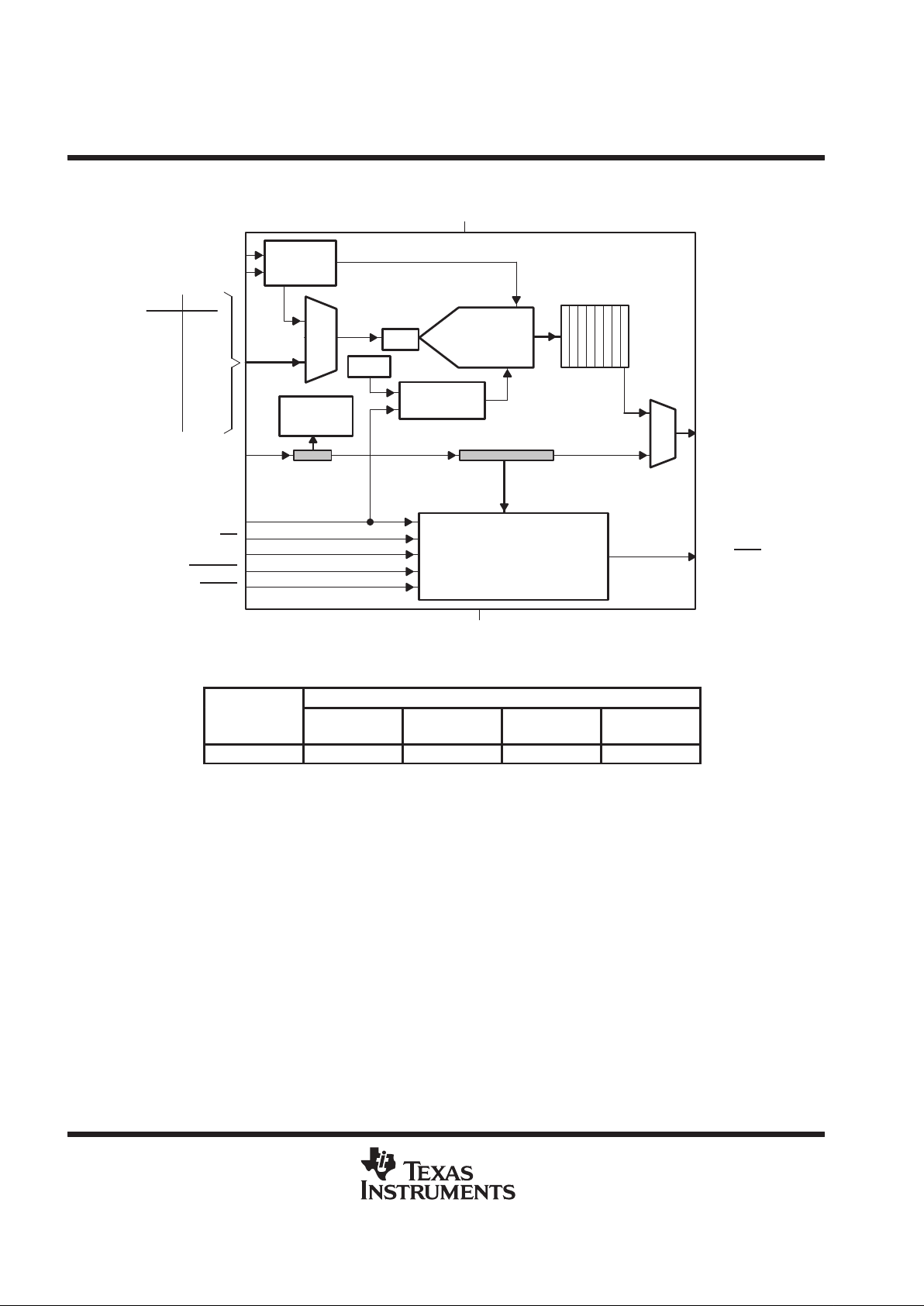
functional block diagram
Command
Decode
SDI
CS
FS
EOC/(INT)
Low Power
10-BIT
SAR ADC
Control Logic
CSTART
PWDN
V
CC
GND
REFP
Analog
MUX
4/2 V
Reference
S/H
OSC
Conversion
Clock
M
U
X
FIFO
10 Bit × 8
CFR
SCLK
SDO
1508
A0
A1
A2
A3
A4
A5
A6
A7
REFM
1504
A0
X
A1
X
A2
X
A3
X
CMR (4 MSBs)
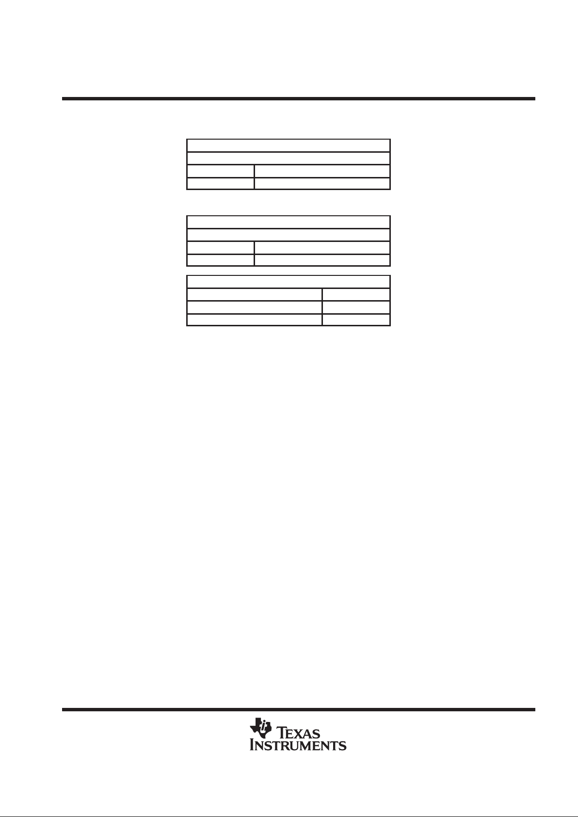
AVAILABLE OPTIONS
PACKAGED DEVICES
T
A
20-TSSOP
(PW)
20-SOIC
(DW)
16-SOIC
(D)
16-TSSOP
(PW)
–40°C to 85°C TLV1508IPW TLV1508IDW TLV1504ID TLV1504IPW
TLV1504, TLV1508
2.7 V TO 5.5 V, 10-BIT, 200 KSPS, 4/8 CHANNEL, LOW POWER,
SERIAL ANALOG-TO-DIGITAL CONVERTERS WITH AUTO POWER DOWN
SLAS251 – DECEMBER 1999
3
POST OFFICE BOX 655303 • DALLAS, TEXAS 75265
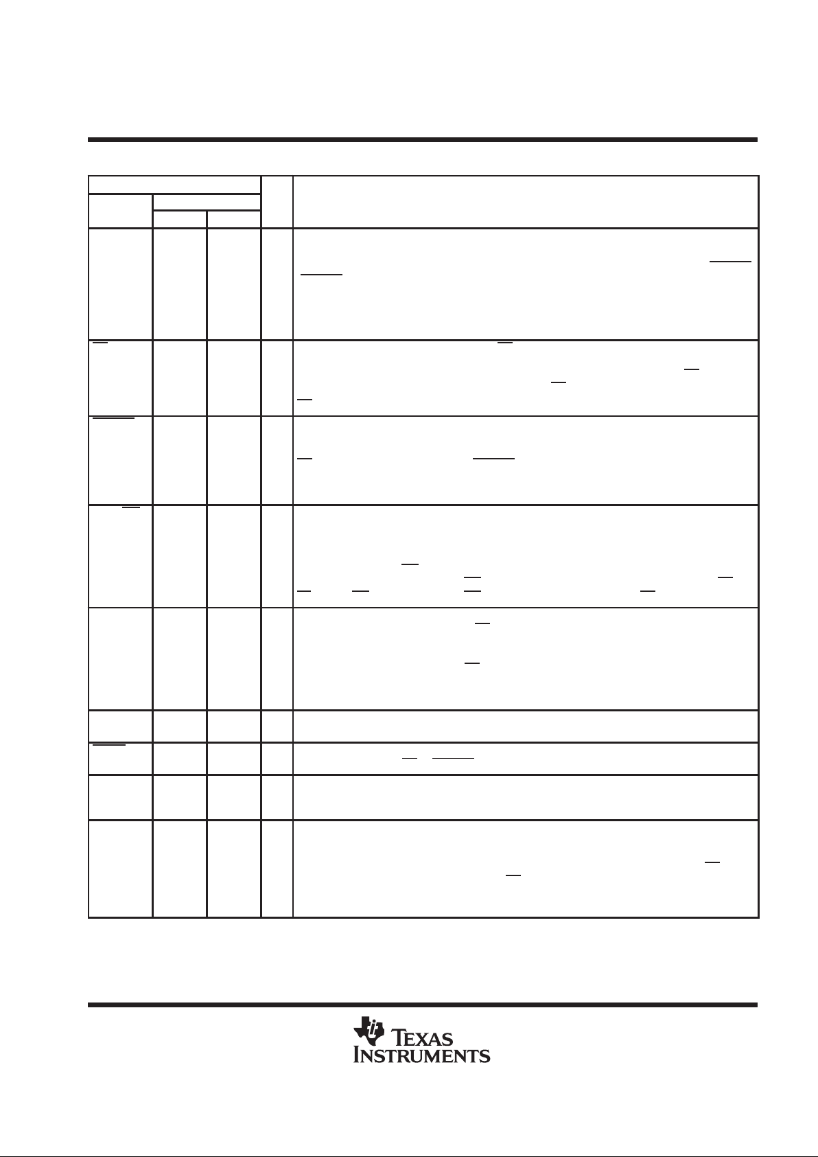
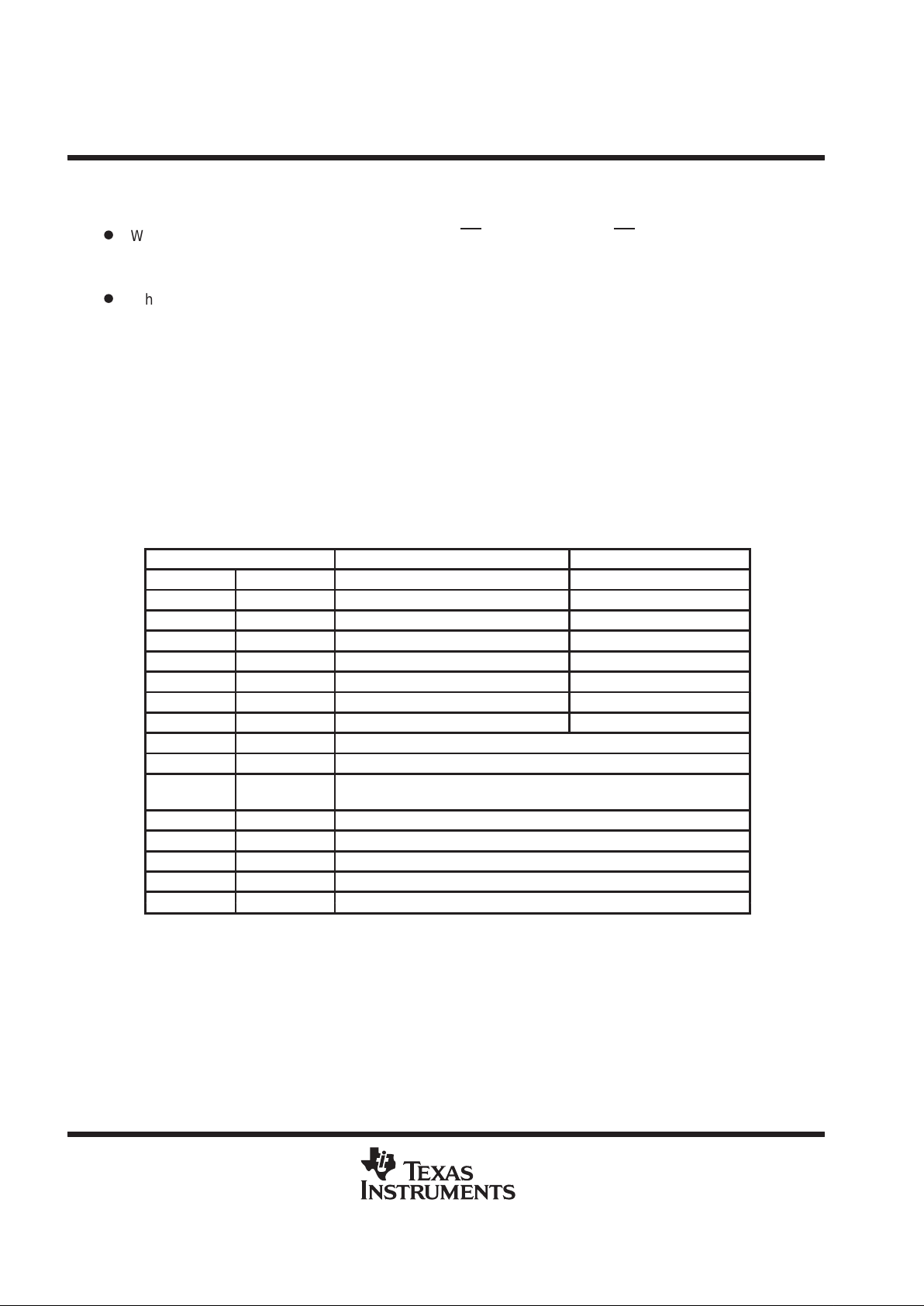
Terminal Functions
TERMINAL
NO.
I/O DESCRIPTION
NAME
TLV1504 TLV1508
A0 A0
A1 A1
A2 A2
A3 A3
A4
A5
A6
A7
6
7
8
9
6
7
8
9
10
11
12
13
I Analog signal inputs. The analog inputs are applied to these terminals and are internally
multiplexed. The driving source impedance should be less than or equal to 1 kΩ.
For a source impedance greater than 1 kΩ, use the asynchronous conversion start signal CST ART
(CSTAR T low time controls the sampling period) or program long sampling period to increase the
sampling time.
CS 16 20 I Chip select. A high-to-low transition on the CS input resets the internal 4-bit counter , enables SDI,
and removes SDO from 3-state within a maximum setup time. SDI is disabled within a setup time
after the 4-bit counter counts to 16 (clock edges) or a low-to-high transition of CS
whichever
happens first. SDO is 3-stated after the rising edge of CS
.
CS
can be used as the FS pin when a dedicated serial port is used.
CSTAR T 10 14 I This terminal controls the start of sampling of the analog input from a selected multiplex channel.
A high-to-low transition starts sampling of the analog input signal. A low-to-high transition puts the
S/H in hold mode and starts the conversion. This input is independent from SCLK and works when
CS
is high (inactive). The low time of CSTAR T controls the duration of the sampling period of the
converter (extended sampling).
Tie this terminal to VCC if not used.
EOC/(INT) 4 4 O End of conversion or interrupt to host processor.
[PROGRAMMED AS EOC]: This output goes from a high-to-low logic level at the end of the
sampling period and remains low until the conversion is complete and data are ready for transfer.
EOC is used in conversion mode 00 only.
[PROGRAMMED AS INT
]: This pin can also be programmed as an interrupt output signal to the
host processor. The falling edge of INT
indicates data are ready for output. The following CS↓ or
FS
↑ clears INT. The falling edge of INT puts SDO back to 3-state even if CS is still active.
FS 13 17 I DSP frame sync input. Indication of the start of a serial data frame in or out of the device. If FS
remains low after the falling edge of CS
, SDI is not enabled until an active FS is presented. A
high-to-low transition on the FS input resets the internal 4-bit counter and enables SDI within a
maximum setup time. SDI is disabled within a setup time after the 4-bit counter counts to 16 (clock
edges) or a low-to-high transition of CS
whichever happens first. SDO is 3-stated after the 16th bit
is presented.
Tie this terminal to VCC if not used.
GND 11 15 I Ground return for the internal circuitry . Unless otherwise noted, all voltage measurements are with
respect to GND.
PWDN 12 16 I Both analog and reference circuits are powered down when this pin is at logic zero. The device can
be restarted by active CS
or CSTART after this pin is pulled back to logic one.
SCLK 3 3 I Input serial clock. This terminal receives the serial SCLK from the host processor. SCLK is used to
clock the input SDI to the input register. When programmed, it may also be used as the source of
the conversion clock.
SDI 2 2 I Serial data input. The input data is presented with the MSB (D15) first. The first 4-bit MSBs,
D(15–12) are decoded as one of the 16 commands (12 only for the TL V1504). All trailing blanks are
filled with zeros. The configure write commands require an additional 12 bits of data.
When FS is not used (FS =1), the first MSB (D15) is expected after the falling edge of CS
and is
shifted in on the rising edges of SCLK (after CS
↓).
When FS is used (typical with an active FS from a DSP) the first MSB (D15) is expected after the
falling edge of FS and is shifted in on the falling edges of SCLK.
TLV1504, TLV1508
2.7 V TO 5.5 V, 10-BIT, 200 KSPS, 4/8 CHANNEL, LOW POWER,
SERIAL ANALOG-TO-DIGITAL CONVERTERS WITH AUTO POWER DOWN
SLAS251 – DECEMBER 1999
4
POST OFFICE BOX 655303 • DALLAS, TEXAS 75265
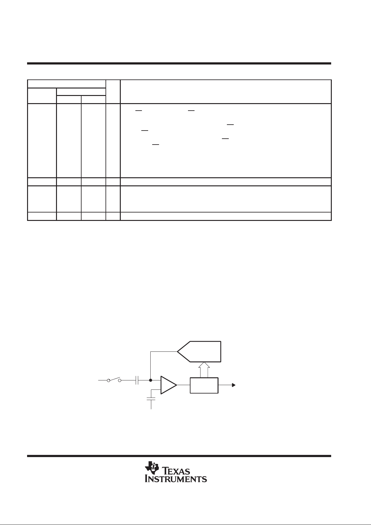
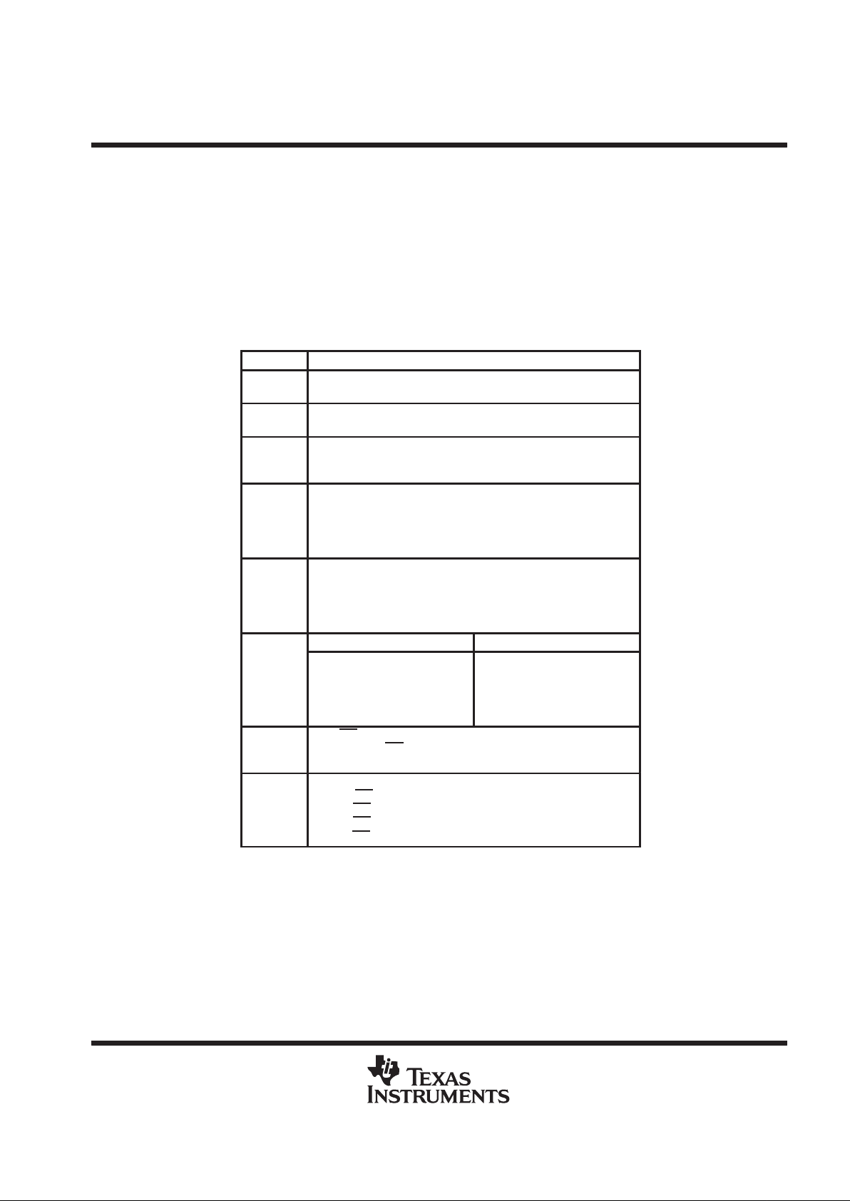
Terminal Functions (Continued)
TERMINAL
NO.
I/O DESCRIPTION
NAME
TLV1504 TLV1508
SDO 1 1 O The 3-state serial output for the A/D conversion result. SDO is kept in the high-impedance state
when CS
is high and after the CS falling edge and until the MSB (D15) is presented. The output
format is MSB (D15) first.
When FS is not used (FS = 1 at the falling edge of CS), the MSB (D15) is presented to the SDO pin
after the CS
falling edge, and successive data are available at the rising edge of SCLK.
When FS is used (FS = 0 at the falling edge of CS
), the MSB (D15) is presented to SDO after the
falling edge of CS
and FS = 0 is detected. Successive data are available at the falling edge of SCLK.
(This is typically used with an active FS from a DSP.)
For conversion and FIFO read cycles, the first 10 bits are the result from the previous conversion
(data) followed by 6 don’t cares. The first four bits from SDO for CFR read cycles should be ignored.
The register content is in the last 12 bits. SDO is 3 stated after the 16th bit.
REFM 14 18 I External reference input or internal reference decoupling.
REFP 15 19 I External reference input or internal reference decoupling. (Shunt capacitors of 10 µF and 0.1 µF
between REFP and REFM.) The maximum input voltage range is determined by the difference
between the voltage applied to this terminal and the REFM terminal when an external reference is
used.
V
CC
5 5 I Positive supply voltage
detailed description
analog inputs and internal test voltages
The 4/8 analog inputs and three internal test inputs are selected by the analog multiplexer depending on the
command entered. The input multiplexer is a break-before-make type to reduce input-to-input noise injection
resulting from channel switching.
converter
The TL V1504/08 uses a 10-bit successive approximation ADC utilizing a charge redistribution DAC. Figure 1
shows a simplified version of the DAC.
The sampling capacitor acquires the signal on Ain during the sampling period. When the conversion process
starts, the SAR control logic and charge redistribution DAC are used to add and subtract fixed amounts of charge
from the sampling capacitor to bring the comparator into a balanced condition. When the comparator is
balanced, the conversion is complete and the ADC output code is generated.
Charge
Redistribution
DAC
Control
Logic
_
+
REFM
Ain
ADC Code
Figure 1. Simplified Model of the Successive-Approximation System
TLV1504, TLV1508
2.7 V TO 5.5 V, 10-BIT, 200 KSPS, 4/8 CHANNEL, LOW POWER,
SERIAL ANALOG-TO-DIGITAL CONVERTERS WITH AUTO POWER DOWN
SLAS251 – DECEMBER 1999
5
POST OFFICE BOX 655303 • DALLAS, TEXAS 75265
detailed description (continued)
serial interface
INPUT DATA FORMAT
MSB LSB
D15–D12 D11–D0
Command Configuration data field
Input data is binary. All trailing blanks can be filled with zeros.
OUTPUT DATA FORMAT READ CFR
MSB LSB
D15–D12 D11–D0
Don’t care Register content
OUTPUT DATA FORMAT CONVERSION/READ FIFO
MSB LSB
D15–D6 D5–D0
Conversion result Don’t care
The output data format is binary (unipolar straight binary).
binary
Zero scale code = 000h, Vcode = VREFM
Full scale code = 3FFh, Vcode = VREFP – 1 LSB
TLV1504, TLV1508
2.7 V TO 5.5 V, 10-BIT, 200 KSPS, 4/8 CHANNEL, LOW POWER,
SERIAL ANALOG-TO-DIGITAL CONVERTERS WITH AUTO POWER DOWN
SLAS251 – DECEMBER 1999
6
POST OFFICE BOX 655303 • DALLAS, TEXAS 75265
control and timing
start of the cycle:
D
When FS is not used ( FS = 1 at the falling edge of CS), the falling edge of CS is the start of the cycle. Input
data is shifted in on the rising edge of SCLK, and output data changes on the falling edge of SCLK. This
is typically used for an SPI microcontroller although it can also be used for a DSP.
D
When FS is used ( FS is an active signal from a DSP), the falling edge of FS is the start of the cycle. Input
data is shifted in on the falling edge, and output data changes on the rising edge of SCLK. This is typically
used for a TMS320 DSP.
first 4-MSBs: the command register (CMR)
The TL V1504/TLV1508 have a 4-bit command set (see Table 1) plus a 12-bit configuration data field. Most of
the commands require only the first 4 MSBs, i.e. without the 12-bit data field.
NOTE:
The device requires a write CFR (configuration register) with 000h data (write A000h to the serial
input) at power up to initialize host select mode.
The valid commands are listed in Table 1.
Table 1. TLV1504/TLV1508 Command Set
SDI D(15–12) BINARY, HEX TLV1508 COMMAND TLV1504 COMMAND
0000b 0000h Select analog input channel 0 Select analog input channel 0
0001b 1000h Select analog input channel 1 N/A
0010b 2000h Select analog input channel 2 Select analog input channel 1
0011b 3000h Select analog input channel 3 N/A
0100b 4000h Select analog input channel 4 Select analog input channel 2
0101b 5000h Select analog input channel 5 N/A
0110b 6000h Select analog input channel 6 Select analog input channel 3
0111b 7000h Select analog input channel 7 N/A
1000b 8000h SW power down (analog + reference)
1001b 9000h Read CFR register data shown as SDO D(11–0)
1010b A000h plus data
Write CFR followed by 12-bit data, e.g., 0A100h means external reference,
short sampling, SCLK/4, single shot, INT
1011b B000h Select test, voltage = (REFP+REFM)/2
1100b C000h Select test, voltage = REFM
1101b D000h Select test, voltage = REFP
1110b E000h FIFO read, FIFO contents shown as SDO D(15–6), D(5–0) = XXXXXX
p
1111b
F000h plus data
Reserved
TLV1504, TLV1508
2.7 V TO 5.5 V, 10-BIT, 200 KSPS, 4/8 CHANNEL, LOW POWER,
SERIAL ANALOG-TO-DIGITAL CONVERTERS WITH AUTO POWER DOWN
SLAS251 – DECEMBER 1999
7
POST OFFICE BOX 655303 • DALLAS, TEXAS 75265
control and timing (continued)
configuration
Configuration data is stored in one 12-bit configuration register (CFR) (see T able 2 for CFR bit definitions). Once
configured after first power up, the information is retained in the H/W or S/W power down state. When the device
is being configured, a write CFR cycle is issued by the host processor. This is a 16-bit write. (If the SCLK stops
after the first 8 bits are entered, then the next eight bits can be taken after the SCLK is resumed.) The status
of the CFR can be read with a read CFR command when the device is programmed for one-shot conversion
mode (CFR D[6,5] = 00).
Table 2. TLV1504/TLV1508 Configuration Register (CFR) Bit Definitions
BIT DEFINITION
D11 Reference select
0: External 1: internal
D10 Internal reference voltage select
0: Internal ref = 4 V 1: internal ref = 2 V
D9 Sample period select
0: Short sampling 12 SCLKs (1x sampling time)
1: Long sampling 24 SCLKs (2x sampling time)
D(8–7) Conversion clock source select
00: Conversion clock = internal OSC
01: Conversion clock = SCLK
10: Conversion clock = SCLK/4
11: Conversion clock = SCLK/2
D(6,5) Conversion mode select
00: Single shot mode (single conversion on selected channel)
01: Repeat mode (repeats conversion on selected channel)
10: Sweep mode (single sweep of selected channels)
11: Repeat sweep mode (repeats sweep of selected channels)
D(4,3)
†
TLV1508 TLV1504
Sweep auto sequence select
00: 0–1–2–3–4–5–6–7
01: 0–2–4–6–0–2–4–6
10: 0–0–2–2–4–4–6–6
11: 0–2–0–2–0–2–0–2
Sweep auto sequence select
00: N/A
01: 0–1–2–3–0–1–2–3
10: 0–0–1–1–2–2–3–3
11: 0–1–0–1–0–1–0–1
D2 EOC/INT – pin function select
0: Pin used as INT
1: Pin used as EOC
D(1,0) FIFO trigger level (sweep sequence length)
00: Full (INT
generated after FIFO level 7 filled)
01: 3/4 (INT
generated after FIFO level 5 filled)
10: 1/2 (INT
generated after FIFO level 3 filled)
11: 1/4 (INT
generated after FIFO level 1 filled)
†
These bits only take effect in conversion modes 10 and 1 1.
sampling
The sampling period starts after the first 4 input data are shifted in if they are decoded as one of the conversion
commands. These are select analog input (channel 0 through 7) and select test (channel 1 through 3).

TLV1504, TLV1508
2.7 V TO 5.5 V, 10-BIT, 200 KSPS, 4/8 CHANNEL, LOW POWER,
SERIAL ANALOG-TO-DIGITAL CONVERTERS WITH AUTO POWER DOWN
SLAS251 – DECEMBER 1999
8
POST OFFICE BOX 655303 • DALLAS, TEXAS 75265
normal sampling
When the converter is using normal sampling, the sampling period is programmable. It can be 12 SCLKs (short
sampling) or 24 SCLKs (long sampling). Long sampling helps the input analog signal sampled to settle to 0.5
LSB accuracy when SCLK is faster than 10 MHz or when input source resistance is high.
extended sampling
An asynchronous (to the SCLK) signal, via dedicated hardware pin CST ART, can be used in order to have total
control of the sampling period and the start of a conversion. This is extended sampling. The falling edge of
CSTART
is the start of the sampling period. The rising edge of CST ART is the end of the sampling period and
the start of the conversion. This function is useful for an application that requires:
D
The use of an extended sampling period to accommodate different input source impedance.
D
The use of a faster I/O clock on the serial port but not enough sampling time is available due to the fixed
number of SCLKs. This could be due to a high input source impedance or due to higher MUX ON resistance
at lower supply voltage (refer to application information).
Once the conversion is complete, the processor can initiate a read cycle using either the read FIFO command
to read the conversion result or simply select the next channel number for conversion. Since the device has a
valid conversion result in the output buffer , the conversion result is simply presented at the serial data output.
CST AR T
is not valid when CS is active.
TLV1504/TLV1508 conversion modes
The TL V1504 and TLV1508 have four dif ferent conversion modes (mode 00, 01, 10, 1 1). The operation of each
mode is slightly different, depending on how the converter performs the sampling and which host interface is
used. The trigger for a conversion can be an active CST AR T (extended sampling), CS (normal sampling, SPI
interface), or FS (normal sampling, TMS320 DSP interface). When FS is used as the trigger, CS can be held
active, i.e. CS
does not need to be toggled through the trigger sequence. Different types of triggers should not
be mixed throughout the repeat and sweep operations. When CST ART is used as the trigger, the conversion
starts on the rising edge of CST ART . The minimum low time for CST AR T is 800 ns. If an active CS or FS is used
as the trigger, the conversion is started after the 16th (short sampling) or 28th (long sampling) SCLK edge.
Enough time (for conversion) should be allowed between consecutive triggers so that no conversion is
terminated prematurely.
one shot mode (mode 00)
One shot mode (mode 00) does not use the FIFO, and the EOC is generated as the conversion is in progress
(or INT is generated after the conversion is done).
repeat mode (mode 01)
Repeat mode (mode 01) uses the FIFO. Once the programmed FIFO threshold is reached, the FIFO must be
read, or the data is lost and the sequence starts over again. This allows the host to set up the converter and
continue monitoring a fixed input and come back to get a set of samples when preferred. The first conversion
must start with a select command so an analog input channel can be selected.
sweep mode (mode 10)
Sweep mode (mode 10) also uses the FIFO. Once it is programmed in this mode, all of the channels listed in
the selected sweep sequence are visited in sequence. The results are converted and stored in the FIFO. This
sweep sequence may not be completed if the FIFO threshold is reached before the list is completed. This allows
the system designer to change the sweep sequence length. Once the FIFO has reached its programmed
threshold, an interrupt (INT) is generated. The host must issue a read FIFO command to read and clear the FIFO
before the next sweep can start.
TLV1504, TLV1508
2.7 V TO 5.5 V, 10-BIT, 200 KSPS, 4/8 CHANNEL, LOW POWER,
SERIAL ANALOG-TO-DIGITAL CONVERTERS WITH AUTO POWER DOWN
SLAS251 – DECEMBER 1999
9
POST OFFICE BOX 655303 • DALLAS, TEXAS 75265
TLV1504/TLV1508 conversion modes (continued)
repeat sweep mode (mode 11)
Repeat sweep mode (mode 1 1) works the same way as mode 10 except the operation has an option to continue
even if the FIFO threshold is reached. Once the FIFO has reached its programmed threshold, an interrupt (INT)
is generated. Then two things may happen:
1. The host may choose to act on it (read the FIFO) or ignore it. If the next cycle is a read FIFO cycle, all of
the data stored in the FIFO is retained until it has been read in order.
2. If the next cycle is not a read FIFO cycle, or another CST ART is generated, all of the content stored in the
FIFO is cleared before the next conversion result is stored in the FIFO, and the sweep is continued.
Table 3. TLV1504/TLV1508 Conversion Mode
CONVERSION
MODE
CFR
D(6,5)
SAMPLING
TYPE
OPERATION
One shot 00
Normal • Single conversion from a selected channel
• CS
or FS to start select/sampling/conversion/read
• One INT
or EOC generated after each conversion
• Host must serve INT
by selecting channel, and converting and reading the previous output.
Extended • Single conversion from a selected channel
• CS
to select/read
• CSTART
to start sampling and conversion
• One INT
or EOC generated after each conversion
• Host must serve INT
by selecting next channel and reading the previous output.
Repeat 01
Normal • Repeated conversions from a selected channel
• CS
or FS to start sampling/conversion
• One INT
generated after FIFO is filled up to the threshold
• Host must serve INT
by either 1) (FIFO read) reading out all of the FIFO contents up to the
threshold, then repeat conversions from the same selected channel or 2) writing another
command(s) to change the conversion mode. If the FIFO is not read when INT
is served, it is
cleared.
Extended • Same as normal sampling except CSTART starts each sampling and conversion when CS is
high.
Sweep 10
Normal • One conversion per channel from a sequence of channels
• CS
or FS to start sampling/conversion
• One INT
generated after FIFO is filled up to the threshold
• Host must serve INT
by (FIFO read) reading out all of the FIFO contents up to the threshold, then
write another command(s) to change the conversion mode.
Extended • Same as normal sampling except CSTART starts each sampling and conversion when CS is
high.
Repeat sweep 11
Normal • Repeated conversions from a sequence of channels
• CS
or FS to start sampling/conversion
• One INT
generated after FIFO is filled up to the threshold
• Host must serve INT
by either 1) (FIFO read) reading out all of the FIFO contents up to the
threshold, then repeat conversions from the same selected channel or 2) writing another
command(s) to change the conversion mode. If the FIFO is not read when INT
is served it is
cleared.
Extended • Same as normal sampling except CSTART starts each sampling and conversion when CS is
high.
NOTE: Programming the EOC/INT pin as the EOC signal works for mode 00 only . The other three modes automatically generate an INT signal
irrespective of whether EOC/INT is programmed.
TLV1504, TLV1508
2.7 V TO 5.5 V, 10-BIT, 200 KSPS, 4/8 CHANNEL, LOW POWER,
SERIAL ANALOG-TO-DIGITAL CONVERTERS WITH AUTO POWER DOWN
SLAS251 – DECEMBER 1999
10
POST OFFICE BOX 655303 • DALLAS, TEXAS 75265
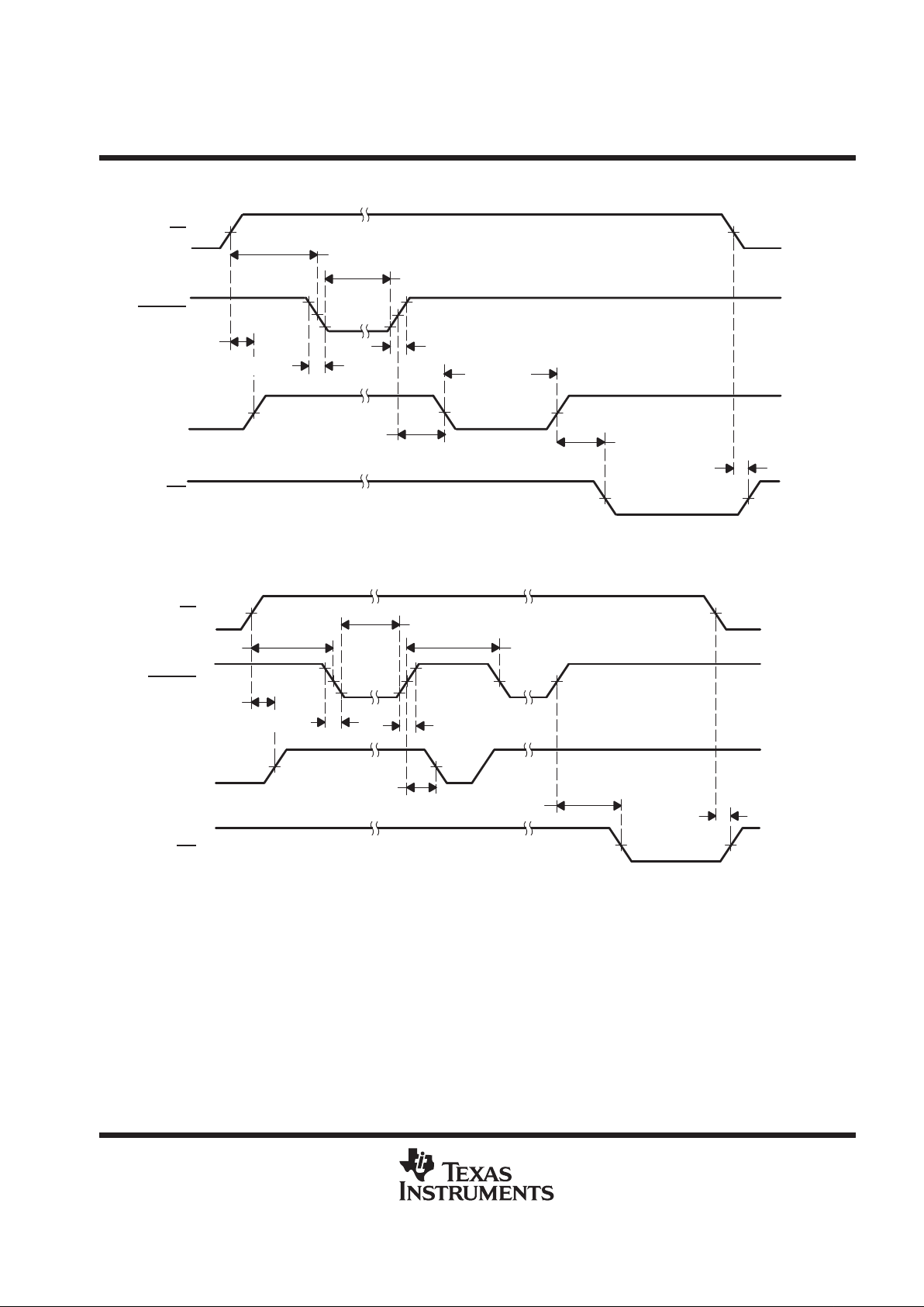
timing diagrams
The timing diagrams can be categorized into two major groups: non conversion and conversion. The
nonconversion cycles are read and write (configuration). None of these cycles carry a conversion. The
conversion cycles are the four modes shown in Figure 7 through Figure 14.
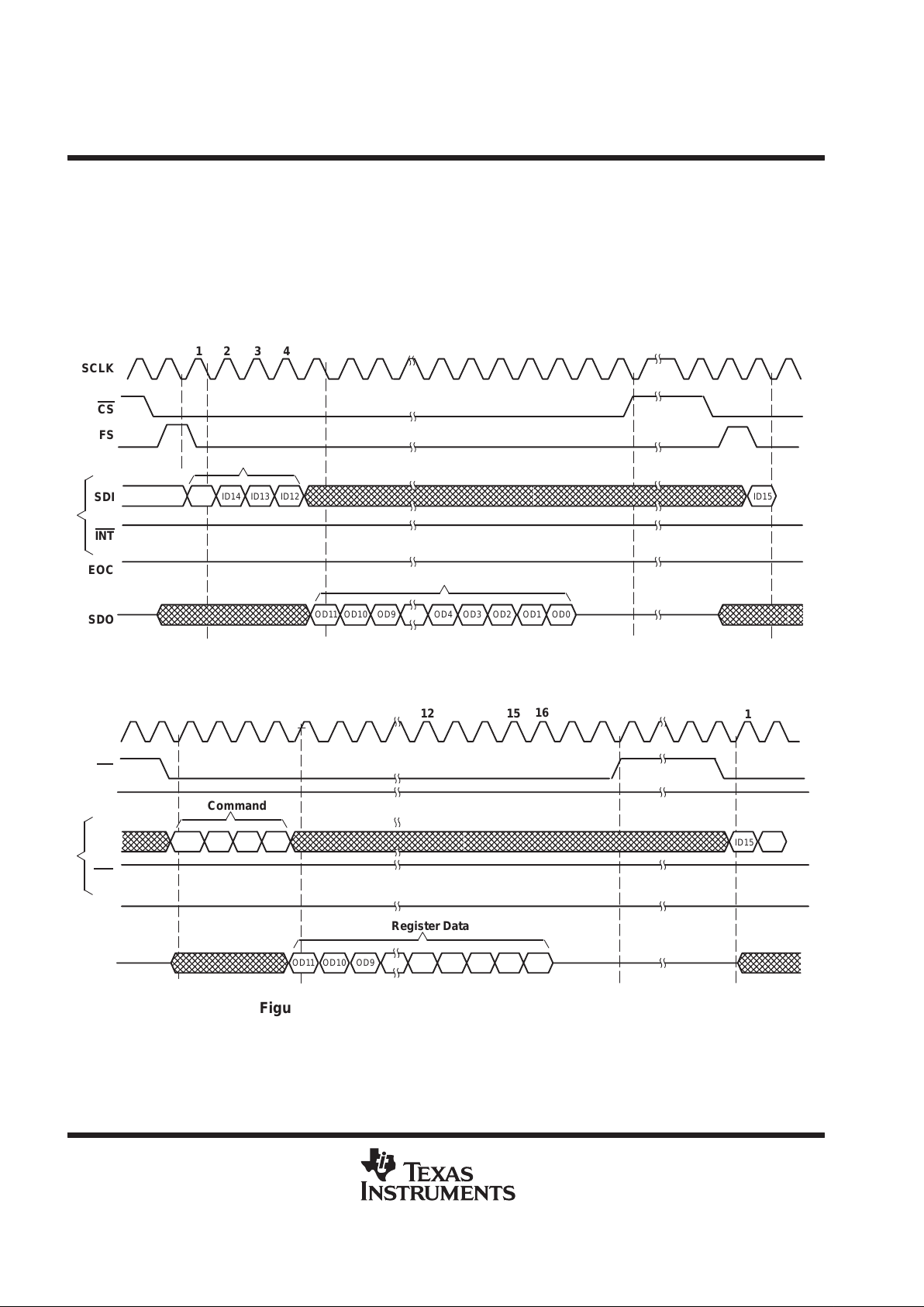
read cycle (read FIFO or read CFR)
read CFR cycle:
The read command is decoded in the first 4 clocks. SDO outputs the contents of the CFR after the 4th SCLK.
SCLK
CS
FS
SDI
INT
EOC
SDO
ID14 ID13 ID12 ID15
OD11 OD10 OD9 OD4 OD3 OD2 OD1 OD0
12 345 6
7131415
16
1
12
ID15
Command
Register Data
Figure 2. TLV1504/TLV1508 Read CFR Cycle (FS active)
SCLK
CS
FS
SDI
INT
EOC
SDO
ID15 ID14 ID13 ID12 ID14
OD4 OD3 OD2 OD1 OD0
12 345 6
7131415
16
1
12
OD11 OD10 OD9
ID15
Command
Register Data
Figure 3. TLV1504/TLV1508 Read CFR Cycle (FS = 1)
TLV1504, TLV1508
2.7 V TO 5.5 V, 10-BIT, 200 KSPS, 4/8 CHANNEL, LOW POWER,
SERIAL ANALOG-TO-DIGITAL CONVERTERS WITH AUTO POWER DOWN
SLAS251 – DECEMBER 1999
11
POST OFFICE BOX 655303 • DALLAS, TEXAS 75265
read cycle (read FIFO or read CFR) (continued)
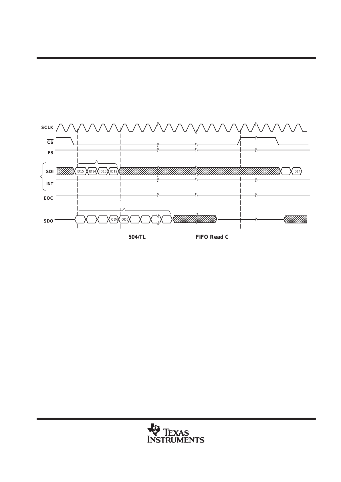
FIFO read cycle
The first command in the active cycle after INT is generated (if the FIFO is used) is assumed as the FIFO read
command. The first FIFO content is output immediately before the command is decoded. If this command is
not a FIFO read, then the output is terminated but the first data in the FIFO is retained until a valid FIFO read
command is decoded. Use of more layers of the FIFO reduces the time taken to read multiple data. This is
because the read cycle does not generate EOC or INT nor does it carry out any conversion.
SCLK
CS
FS
SDI
INT
EOC
SDO
ID15 ID14 ID13 ID12 ID14
OD6 OD5 OD3 OD0
12 345 6
7111215
16
1
10
OD9 OD8 OD7
ID15
OD4
Command
FIFO Data
Figure 4. TLV1504/TLV1508 Continuous FIFO Read Cycle (FS = 1)
(controlled by SCLK, SCLK can stop between each 16 SCLKs)
TLV1504, TLV1508
2.7 V TO 5.5 V, 10-BIT, 200 KSPS, 4/8 CHANNEL, LOW POWER,
SERIAL ANALOG-TO-DIGITAL CONVERTERS WITH AUTO POWER DOWN
SLAS251 – DECEMBER 1999
12
POST OFFICE BOX 655303 • DALLAS, TEXAS 75265
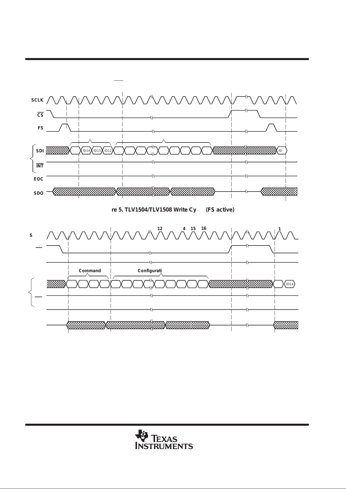
write cycle (write CFR)
The write cycle is used to write to the configuration register CFR (with 12-bit register content). The write cycle
does not generate an EOC or INT
nor does it carry out any conversion.
SCLK
CS
FS
SDI
INT
EOC
SDO
ID14 ID13 ID12 ID15
ID11 ID10 ID9 ID4 ID3 ID2 ID1 ID0
12 345 6
7131415
16
1
12
ID15
Command Configuration Data
Figure 5. TLV1504/TLV1508 Write Cycle (FS active)
SCLK
CS
FS
SDI
INT
EOC
SDO
ID15 ID14 ID13 ID12 ID15
ID11 ID10 ID9 ID4 ID3 ID2 ID1 ID0
12 345 6
7131415
16
1
12
ID14
Command Configuration Data
Figure 6. TLV1504/TLV1508 Write Cycle (FS = 1)
TLV1504, TLV1508
2.7 V TO 5.5 V, 10-BIT, 200 KSPS, 4/8 CHANNEL, LOW POWER,
SERIAL ANALOG-TO-DIGITAL CONVERTERS WITH AUTO POWER DOWN
SLAS251 – DECEMBER 1999
13
POST OFFICE BOX 655303 • DALLAS, TEXAS 75265
conversion cycles
DSP/normal sampling
SCLK
CS
FS
SDI
INT
EOC
SDO
ID15 ID14 ID13 ID12
OD9 OD8 OD6 OD5 OD4 OD3
1 2 3 4 5 7 11 12 15 16 110 28
OD7
t
sample
(Long)
t
sample
(Short)
6
ID15
OD0
t
conv
t
conv
Command
Previous Conversion Result
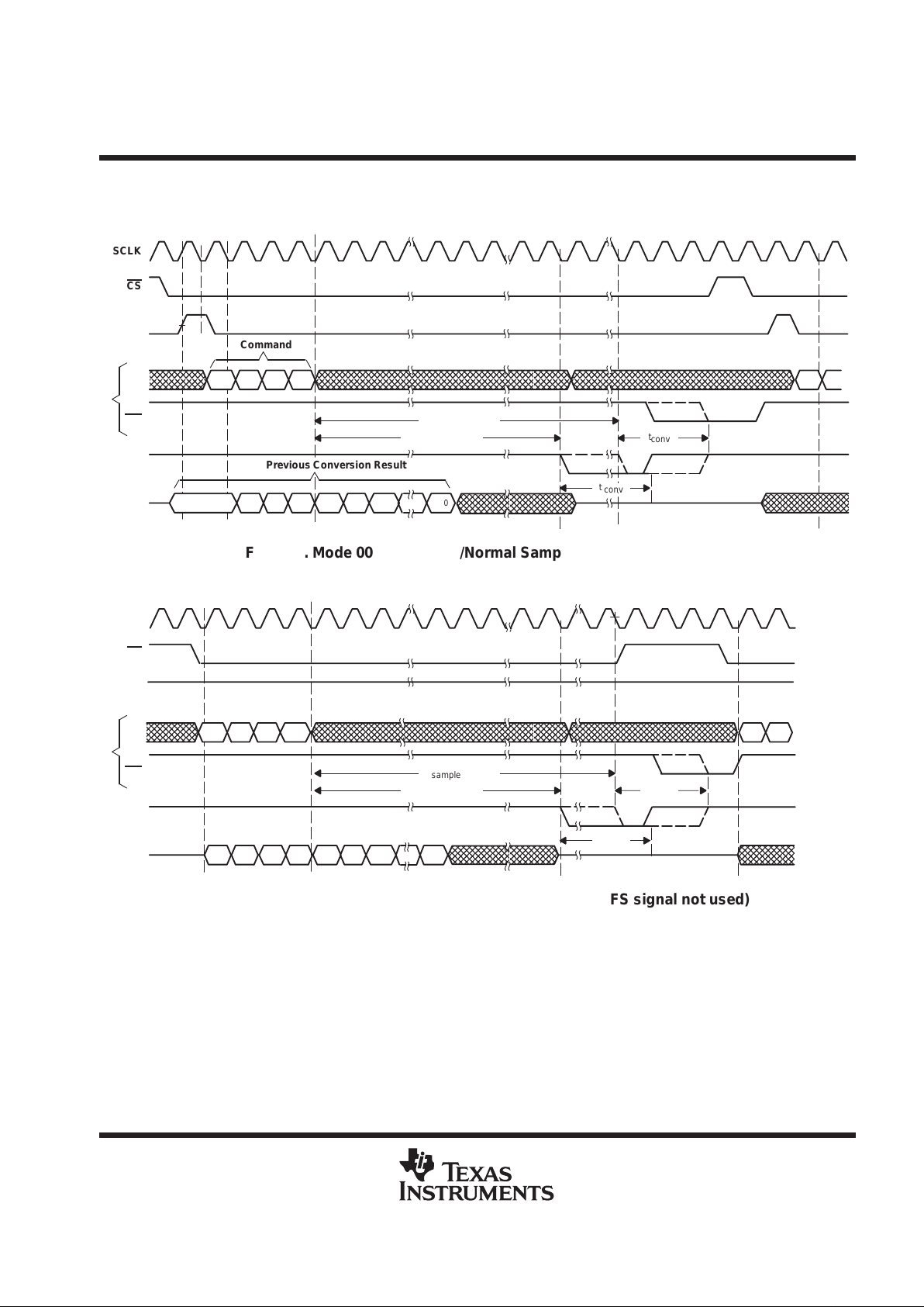
Figure 7. Mode 00 Single Shot/Normal Sampling (FS signal used)
SCLK
CS
FS
SDI
INT
EOC
SDO
ID15 ID14 ID13 ID12
OD8
OD6 OD5 OD4 OD3
1 2 3 4 5 7 11 12 15 16 110 28
OD7
t
sample
(Long)
t
sample
(Short)
6
ID15
OD0
t
conv
t
conv
OD9
ID14
Figure 8. Mode 00 Single Shot/Normal Sampling (FS = 1, FS signal not used)

TLV1504, TLV1508
2.7 V TO 5.5 V, 10-BIT, 200 KSPS, 4/8 CHANNEL, LOW POWER,
SERIAL ANALOG-TO-DIGITAL CONVERTERS WITH AUTO POWER DOWN
SLAS251 – DECEMBER 1999
14
POST OFFICE BOX 655303 • DALLAS, TEXAS 75265
conversion cycles (continued)
CS
CSTART
SDI
INT
EOC
SDO
Hi-Z
Select/Read
Cycle
Select/Read
Cycle
t
sample
t
convert
†
Previous Conversion
Result
Previous Conversion
Result
FS
Hi-Z Hi-Z
†
This is one of the single shot commands. Conversion starts on next rising edge of CSTAR T.
Figure 9. Mode 00 Single Shot/Extended Sampling (FS signal used, FS pin connected to TMS320 DSP)
CS used as FS input
When interfacing with the TMS320 DSP using conversion mode 00, the FSR signal from the DSP may be
connected to the CS input if this is the only device on the serial port. This will save one output pin from the DSP .
Output data is made available on the rising edge of SCLK and input data is latched on the rising edge of SCLK
in this case.
modes using the FIFO: modes 01, 10, 11 timing
Modes 01, 10, and 11 timing are very similar except for how and when the FIFO is read, how the device is
configured, and how channel(s) are selected.
Mode 01 (repeat mode) requires a two-cycle configuration where the first one sets the mode and the second
one selects the channel. Once the FIFO is filled up to the threshold programmed, it has the option to either read
the FIFO or configure for other modes. Therefore, the sequence is either configure: select : triggered
conversions : FIFO read : select : triggered conversions : FIFO read or configure : select : triggered conversions
: configure : .... Each configure clears the FIFO and the action that follows the configure command depends on
the mode setting of the device.
NOTE:
When using CSTAR T
to sample in extended mode, the falling edge of the 1st CSTAR T trigger should
occur no more than 2.5 µs after the falling CS edge (or falling FS edge if FS is active) of the channel
select cycle (see Figure 11).
TLV1504, TLV1508
2.7 V TO 5.5 V, 10-BIT, 200 KSPS, 4/8 CHANNEL, LOW POWER,
SERIAL ANALOG-TO-DIGITAL CONVERTERS WITH AUTO POWER DOWN
SLAS251 – DECEMBER 1999
15
POST OFFICE BOX 655303 • DALLAS, TEXAS 75265
modes using the FIFO: modes 01, 10, 11 timing (continued)
CS
CSTART
SDI
INT
SDO
Hi-Z
From Channel 2
t
convert
FS
†
§
‡‡‡‡ §
Hi-Z
t
sample
t
sample
t
sample
t
convert
Configure Select
Conversion #1
Select
Conversion #4
Read FIFO #1 #2 #3 #4 Next #1
Top of FIFO
From Channel 2
t
convert
†
Command = Configure write for mode 01, FIFO threshold = 1/2
‡
Command = Read FIFO, 1st FIFO read
§
Command = Select ch2.
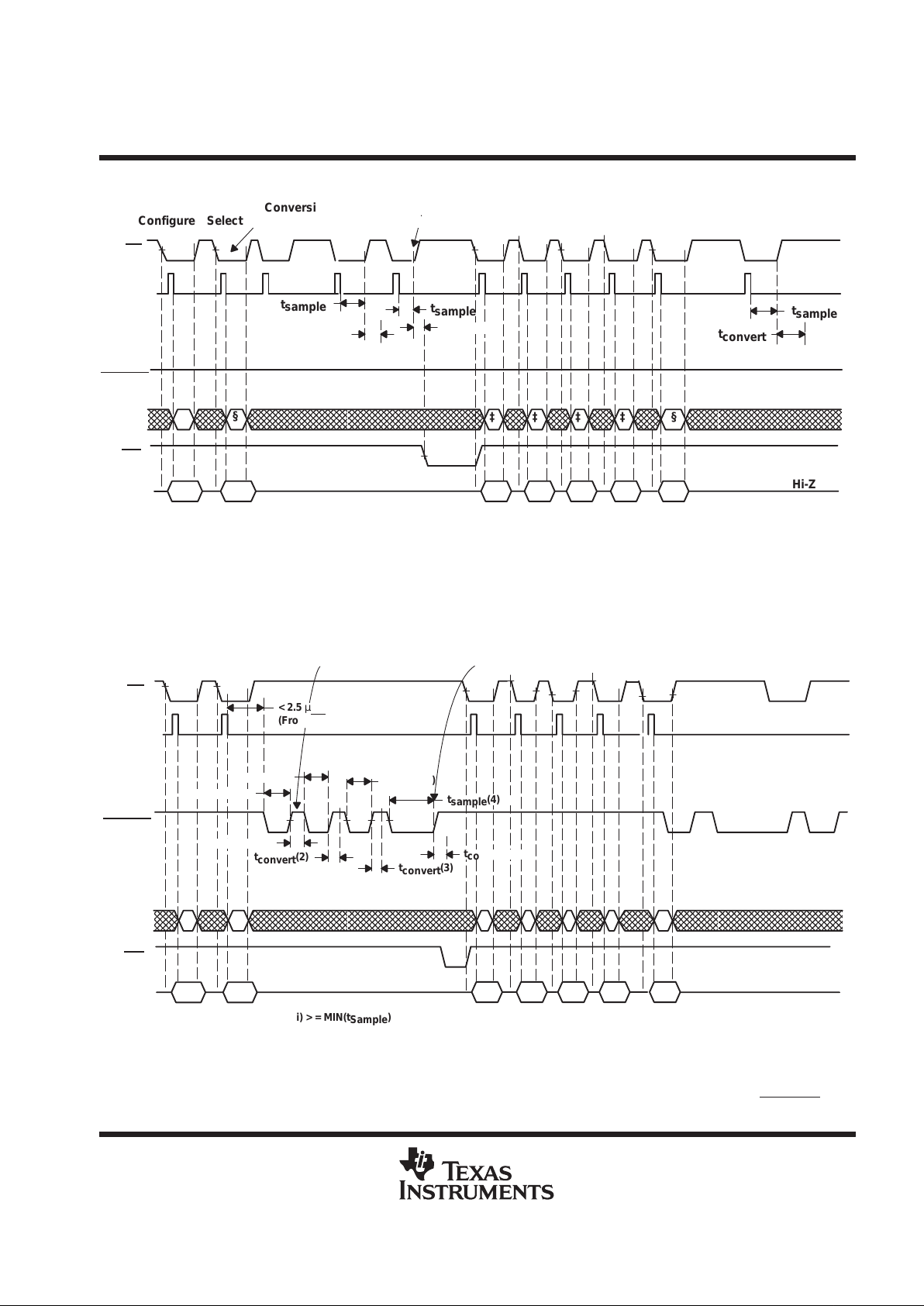
Figure 10. TL V1504/TLV1508 Mode 01 DSP Serial Interface (Conversions triggered by FS)
CS
CSTART
SDI
INT
SDO
Hi-Z
From Channel 2
FS
(DSP)
From Channel 2
Configure Select
Conversion #1
Select
Conversion #4
Read FIFO
First FIFO Read
‡‡‡ ‡ §
#1 #2 #3 #4 Next #1
†
t
sample
(1)
t
convert
(1)
§
t
sample
(2)
t
sample
(3)
t
sample
(4)
t
convert
(2)
t
convert
(3)
t
convert
(4)
Hi-Z
t
Sample
(i) > = MIN(t
Sample
)
< 2.5 µs
(From CS
↓ if FS = 1)
†
Command = Configure write for mode 01, FIFO threshold = 1/2
‡
Command = Read FIFO, 1st FIFO read
§
Command = Select ch2.
Figure 11. TLV1504/TLV1508 Mode 01 µp/DSP Serial Interface (Conversions triggered by CSTART)
TLV1504, TLV1508
2.7 V TO 5.5 V, 10-BIT, 200 KSPS, 4/8 CHANNEL, LOW POWER,
SERIAL ANALOG-TO-DIGITAL CONVERTERS WITH AUTO POWER DOWN
SLAS251 – DECEMBER 1999
16
POST OFFICE BOX 655303 • DALLAS, TEXAS 75265
modes using the FIFO: modes 01, 10, 11 timing (continued)
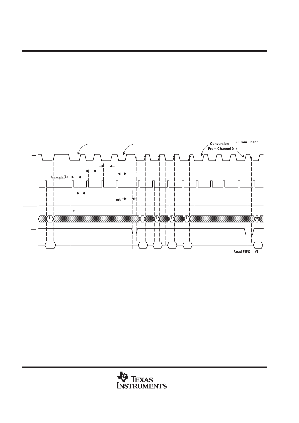
Mode 10 (sweep mode) requires reconfiguration at the start of each new sweep sequence. Once the FIFO is
filled up to the programmed threshold, the host has the option to either read the FIFO or configure for other
modes. Once the FIFO is read, the host must reconfigure the device before the next sweep sequence can be
started. So the sequence is either configure : triggered conversions : FIFO read : configure. or configure :
triggered conversions : configure : .... Each configure clears the FIFO and the action that follows the configure
command depends on the mode setting of the device.
Mode 1 1 (repeat sweep mode) requires one cycle configuration. This sweep sequence can be repeated without
reconfiguration. Once the FIFO is filled up to the programmed threshold, the host has the option to either read
the FIFO or configure for other modes. So the sequence is either configure : triggered conversions : FIFO read
: triggered conversions : FIFO read ... or configure : triggered conversions : configure : .... Each configure clears
the FIFO and the action that follows the configure command depends on the mode setting of the device.
CS
CSTART
SDI
INT
SDO
From Channel 0
FS
(DSP)
From Channel 3
Configure
Conversion
Conversion
Read FIFO #1 #2 #3 #4
Top of FIFO
‡
‡
†
‡‡‡
t
sample
(1)
Read FIFO #1
From Channel 0
Conversion
From Channel 3
Conversion
Repeat
Second FIFO Read
Repeat
t
sample
(2)
t
sample
(3)
t
sample
(4)
First FIFO Read
t
convert
t
convert
t
Sample
(i) > = MIN(t
Sample
)
†
Command = Configure write for mode 10 or 1 1, FIFO threshold = 1/2, sweep seq = 0–1–2–3.
‡
Command = Read FIFO
Figure 12. TLV1504/TLV1508 Mode 10/11 DSP Serial Interface (Conversions triggered by FS)
TLV1504, TLV1508
2.7 V TO 5.5 V, 10-BIT, 200 KSPS, 4/8 CHANNEL, LOW POWER,
SERIAL ANALOG-TO-DIGITAL CONVERTERS WITH AUTO POWER DOWN
SLAS251 – DECEMBER 1999
17
POST OFFICE BOX 655303 • DALLAS, TEXAS 75265
modes using the FIFO: modes 01, 10, 11 timing (continued)
t
sample
(3)
CS
CSTART
SDI
INT
SDO
From Channel 0
FS
(DSP)
Configure
Conversion
Read FIFO #1 #2 #3 #4
Top of FIFO
Read FIFO #1
From Channel 0
Conversion
Repeat
First FIFO Read
Second FIFO Read
Repeat
‡
‡
†
‡‡ ‡
t
sample
(i) >= MIN (t
sample
)
t
sample
(2)
t
sample
(4)
t
convert
From Channel 3
Conversion
Conversion
From Channel 3
ОООООООООООО
t
convert
t
sample
(1)
†
Command = Configure write for mode 10 or 1 1, FIFO threshold = 1/2, sweep seq = 0–1–2–3.
‡
Command = Read FIFO
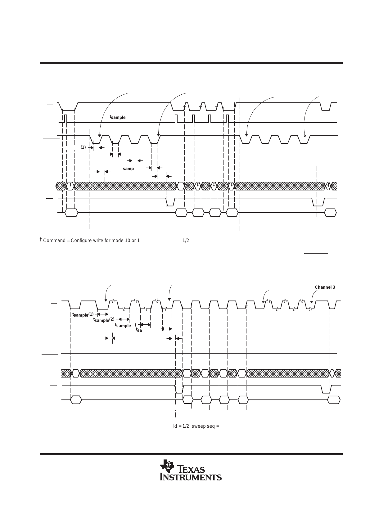
Figure 13. TLV1504/TLV1508 Mode 10/11 DSP Serial Interface (Conversions triggered by CSTART)
CS
CSTART
SDI
INT
SDO
From Channel 0
t
convert
Configure
Conversion
Conversion
Read FIFO #1 #2 #3 #4
Top of FIFO
Read FIFO #1
Conversion
Conversion
Repeat
First FIFO Read
Second FIFO Read
Repeat
‡
‡
†
‡‡‡
t
Sample
(i) > = MIN(t
Sample
)
From Channel 3
From Channel 0
From Channel 3
t
sample
(1)
t
sample
(2)
t
sample
(3)
t
sample
(4)
t
convert
†
Command = Configure write for mode 10 or 1 1, FIFO threshold = 1/2, sweep seq = 0–1–2–3.
‡
Command = Read FIFO
Figure 14. TLV1504/TLV1508 Mode 10/11 µp Serial Interface (Conversions triggered by CS)
TLV1504, TLV1508
2.7 V TO 5.5 V, 10-BIT, 200 KSPS, 4/8 CHANNEL, LOW POWER,
SERIAL ANALOG-TO-DIGITAL CONVERTERS WITH AUTO POWER DOWN
SLAS251 – DECEMBER 1999
18
POST OFFICE BOX 655303 • DALLAS, TEXAS 75265
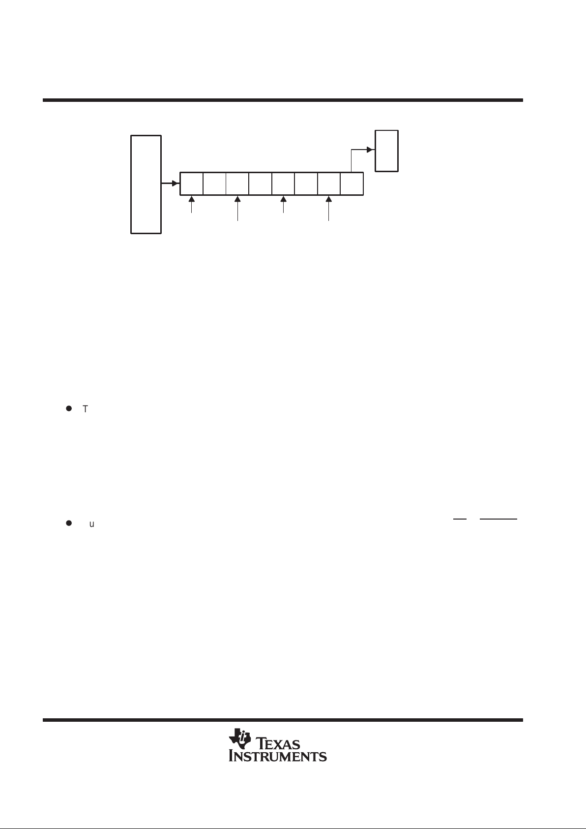
FIFO operation
76543210ADC
10-BIT×8
FIFO
OD
Serial
FIFO Full
FIFO 3/4 Full
FIFO 1/2 Full
FIFO 1/4 Full
FIFO Threshold Pointer
Figure 15. TLV1504/TLV1508 FIFO
The device has an 8 layer FIFO that can be programmed for different thresholds. An interrupt is sent to the host
after the preprogrammed threshold is reached. The FIFO can be used to store data from either a fixed channel
or a series of channels based on a preprogrammed sweep sequence. For example, an application may require
eight measurements from channel 3. In this case, the FIFO is filled with 8 data sequentially taken from channel
3. Another application may require data from channel 0, channel 2, channel 4, and channel 6 in an orderly
manner. Therefore, the threshold is set for 1/2 and the sweep sequence 0–2–4–6–0–2–4–6 is chosen. An
interrupt is sent to the host as soon as all four data samples are in the FIFO.
SCLK and conversion speed
There are multiple ways to adjust the conversion speed.
D
The SCLK can be used as the source of the conversion clock.
The onboard OSC is approximately 4 MHz and 13 conversion clocks are required to complete a conversion.
(Corresponding 3.25 µs conversion time). The devices can operate with an SCLK up to 20 MHz for the
supply voltage range specified. When a more accurate conversion time is desired, the SCLK can be used as
the source of the conversion clock. The clock divider provides speed options appropriate for an application
where a high speed SCLK is used for faster I/O. The total conversion time is 13 ×(DIV/f
SCLK
) where DIV is 1,
2, or 4. For example a 20 MHz SCLK with the divide by 4 option produces a {13 × (4/20 M) = 2.6 µs}
conversion time. When an external serial clock (SCLK) is used as the source of the conversion clock, the
maximum equivalent conversion clock (f
SCLK
/DIV) should not exceed 6 MHz.
D
Auto power down can be used. This mode is always on. If the device is not accessed (by CS or CST ART),
the converter is powered down to save power. The built-in reference is left on in order to quickly resume
operation within one half SCLK period. This provides unlimited choices to trade speed with power savings.
reference voltage
The device has a built-in reference with a programmable level of 2 V or 4 V. If the internal reference is used,
REFP is set to 2 V or 4 V and REFM is set to 0 V . An external reference can also be used through two reference
input pins, REFP and REFM, if the reference source is programmed as external. The voltage levels applied to
these pins establish the upper and lower limits of the analog inputs to produce a full-scale and zero-scale
reading respectively . The values of REFP, REFM, and the analog input should not exceed the positive supply
or be lower than GND consistent with the specified absolute maximum ratings. The digital output is at full scale
when the input signal is equal to or higher than REFP and at zero when the input signal is equal to or lower than
REFM.

TLV1504, TLV1508
2.7 V TO 5.5 V, 10-BIT, 200 KSPS, 4/8 CHANNEL, LOW POWER,
SERIAL ANALOG-TO-DIGITAL CONVERTERS WITH AUTO POWER DOWN
SLAS251 – DECEMBER 1999
19
POST OFFICE BOX 655303 • DALLAS, TEXAS 75265
FIFO operation (continued)
power down
Writing 8000h to the device puts the device into a software power down state. For a hardware powerdown, the
dedicated PWDN pin provides another way to power down the device asynchronously . These two power down
modes power down the entire device including the built-in reference to save power. The internal reference
requires 20 ms to resume from either a software or hardware power down state.
Auto power down mode is always enabled. This mode maintains the built-in reference if an internal reference
is used so resumption is fast enough to be used between cycles.
The configuration register is not affected by any of the power down modes but the sweep operation sequence
has to be started over again. All FIFO contents are cleared by the hardware and software power down modes.
power up and initialization
Initialization requires:
1. Determine processor type by writing A000h to the TLV1504/08
2. Configure the device
The first conversion after power up or resuming from power down is not valid.
absolute maximum ratings over operating free-air temperature (unless otherwise noted)
†
Supply voltage range, GND to VCC –0.3 V to 6.5 V. . . . . . . . . . . . . . . . . . . . . . . . . . . . . . . . . . . . . . . . . . . . . . . . .
Analog input voltage range –0.3 V to V
CC
+ 0.3 V. . . . . . . . . . . . . . . . . . . . . . . . . . . . . . . . . . . . . . . . . . . . . . . . . . .
Reference input voltage V
CC
+ 0.3 V. . . . . . . . . . . . . . . . . . . . . . . . . . . . . . . . . . . . . . . . . . . . . . . . . . . . . . . . . . . . .
Digital input voltage range –0.3 V to V
CC
+ 0.3 V. . . . . . . . . . . . . . . . . . . . . . . . . . . . . . . . . . . . . . . . . . . . . . . . . . .
Operating virtual junction temperature range, TJ –40°C to 150°C. . . . . . . . . . . . . . . . . . . . . . . . . . . . . . . . . . . . .
Operating free-air temperature range, T
A
: TLV1504/08I –40°C to 85°C. . . . . . . . . . . . . . . . . . . . . . . . . . . . . . .
Storage temperature range, T
stg
–65°C to 150°C. . . . . . . . . . . . . . . . . . . . . . . . . . . . . . . . . . . . . . . . . . . . . . . . . . .
Lead temperature 1,6 mm (1/16 inch) from case for 10 seconds 260°C. . . . . . . . . . . . . . . . . . . . . . . . . . . . . . .
†
Stresses beyond those listed under “absolute maximum ratings” may cause permanent damage to the device. These are stress ratings only, and
functional operation of the device at these or any other conditions beyond those indicated under “recommended operating conditions” is not
implied. Exposure to absolute-maximum-rated conditions for extended periods may affect device reliability.
recommended operating conditions
MIN NOM MAX UNIT
Supply voltage, V
CC
2.7 3.3 5.5 V
Positive external reference voltage input, V
REFP
(see Note 1) 2 V
CC
V
Negative external reference voltage input, V
REFM
(note Note 1) 0 2 V
Differential reference voltage input, V
REFP
– V
REFM
(see Note 1) 2 VCCVCC+0.2 V
Analog input voltage (see Note 1) 0 V
CC
V
High level control input voltage, V
IH
2.1 V
Low-level control input voltage, V
IL
0.6 V
Rise time, for CS, CSTART SDI at 0.5 pF, t
r(I/O)
4.76 ns
Fall time, for CS, CSTART SDI at 0.5 pF, t
f(I/O)
2.91 ns
Rise time, for INT, EOC, SDO at 30 pF, t
r(Output)
2.43 ns
Fall time, for INT, EOC, SDO at 30 pF, t
f(Output)
2.3 ns
NOTE 1: When binary output format is used, analog input voltages greater than that applied to REFP convert as all ones (1 111111111), while input
voltages less than that applied to REFM convert as all zeros (0000000000). The device is functional with reference down to 2 V (V
REFP
– V
REFM
–1); however, the electrical specifications are no longer applicable.
TLV1504, TLV1508
2.7 V TO 5.5 V, 10-BIT, 200 KSPS, 4/8 CHANNEL, LOW POWER,
SERIAL ANALOG-TO-DIGITAL CONVERTERS WITH AUTO POWER DOWN
SLAS251 – DECEMBER 1999
20
POST OFFICE BOX 655303 • DALLAS, TEXAS 75265
recommended operating conditions (continued)
MIN NOM MAX UNIT
Transition time, for FS, SCLK, SDI, t
t(SCLK)
0.5 SCLK
Setup time, CS falling edge before SCLK rising edge (FS=1) or before SCLK falling edge (when FS is active),
t
su(CS-SCLK)
0.5 SCLK
Hold time, CS rising edge after SCLK rising edge (FS=1) or after SCLK falling edge (when FS is active),
t
h(SCLK-CS)
5 ns
Delay time, delay from CS falling edge to FS rising edge, t
d(CSL-FSH)
0.5 7 SCLKs
Delay time, delay time from 16th SCLK falling edge to CS rising edge (FS is active), t
d(SCLK16L-CSH)
0.5 SCLKs
Setup time, FS rising edge before SCLK falling edge, t
su(FSH-SCLKL)
0.25 0.75 SCLKs
Hold time, FS hold high after SCLK falling edge, t
h(FSH-SCLKL)
0.25 0.75 SCLKs
Pulse width, CS high time, t
wH(CS)
100 ns
SCLK cycle time, VCC = 2.7 V to 3.6V, t
c(SCLK)
67 ns
SCLK cycle time, VCC = 4.5 V to 5.5V, t
c(SCLK)
50 ns
Pulse width, SCLK low time, t
wL(SCLK)
20 30 ns
Pulse width, SCLK high time, t
wH(SCLK)
20 30 ns
Setup time, SDI valid before falling edge of SCLK (FS is active) or the rising edge of SCLK (FS=1),
t
su(DI-SCLK)
25 ns
Hold time, SDI hold valid after falling edge of SCLK (FS is active) or the rising edge of SCLK (FS=1),
t
h(DI-SCLK)
5 ns
Delay time, delay from CS falling edge to SDO valid, t
d(CSL-DOV)
1 25 ns
Delay time, delay from FS falling edge to SDO valid, t
d(FSL-DOV)
1 25 ns
Delay time, delay from SCLK rising edge (FS is active) or SCLK falling edge (FS=1) SDO valid, t
d(SCLK-DOV)
1 25 ns
Delay time, delay from CS rising edge to SDO 3-stated, t
d(CSH-DOZ)
1 25 ns
Delay time, delay from 16th SCLK falling edge (FS is active) or the 16th rising edge (FS=1) to EOC falling
edge, t
d(SCLK-EOCL)
1 25 ns
Delay time, delay from EOC rising edge to SDO 3-stated if CS is low, t
d(EOCH-DOZ)
1 50 ns
Delay time, delay from 16th SCLK rising edge to INT falling edge (FS =1) or from the 16th falling edge SCLK
to INT falling edge (when FS active), t
d(SCLK-INTL)
3.5 µs
Delay time, delay from CS falling edge to INT rising edge, t
d(CSL-INTH)
1 50 ns
Delay time, delay from CS rising edge to CSTAR T falling edge, t
d(CSH-CSTAR TL)
100 ns
Delay time, delay from CSTAR T rising edge to EOC falling edge, t
d(CSTAR TH-EOCL)
1 50 ns
Pulse width, CSTAR T low time, twL(CSTAR T) 0.8 µs
Delay time, delay from CS rising edge to EOC rising edge, t
d(CSH-EOCH)
1 50 ns
Delay time, delay from CSTAR T rising edge to CSTART falling edge, t
d(CSTAR TH-CSTARTL)
3.6 µs
Delay time, delay from CSTAR T rising edge to INT falling edge, t
d(CSTAR TH-INTL)
3.5 µs
Operating free-air temperature, T
A
TLV1504I/TLV1508I –40 85
_
C
NOTE 2: This is the time required for the clock input signal to fall from VIH max or to rise from VILmax to VIHmin. In the vicinity of normal room
temperature, the devices function with input clock transition time as slow as 1 µs for remote data-acquisition applications where the
sensor and A/D converter are placed several feet away from the controlling microprocessor.
TLV1504, TLV1508
2.7 V TO 5.5 V, 10-BIT, 200 KSPS, 4/8 CHANNEL, LOW POWER,
SERIAL ANALOG-TO-DIGITAL CONVERTERS WITH AUTO POWER DOWN
SLAS251 – DECEMBER 1999
21
POST OFFICE BOX 655303 • DALLAS, TEXAS 75265
electrical characteristics over recommended operating free-air temperature range, V
CC
= V
REFP
= 2.7 V to
5.5 V, SCLK frequency = 20 MHz at 5 V, 15 MHz at 3 V (unless otherwise noted)
PARAMETER TEST CONDITIONS MIN TYP† MAX UNIT
p
V
CC
= 5.5 V, IOH = –0.2 mA at 30 pF load 2.4
VOHHigh-level output voltage
V
CC
= 2.7 V, IOH = -20 µA at 30 pF load VCC–0.2
V
p
V
CC
= 5.5 V, IOL = 0.8 mA at 30 pF load 0.4
VOLLow-level output voltage
V
CC
= 2.7 V, IOL = 20 µA at 30 pF load 0.1
V
Off-state output current
VO = V
CC
1 2.5
I
OZ
O saeou u cu e
(high-impedance-state)
V
O
= 0
CS
=
V
CC
–1 –2.5
µ
A
I
IH
High-level input current V
I
= V
CC
0.005 2.5 µA
I
IL
Low-level input current V
I
= 0 V –0.005 2.5 µA
VCC = 4.5 V to 5.5 V 1.3
Operating supply current, normal samplin
g
CS at 0 V, Ext ref
VCC = 2.7 V to 3.3 V 0.95
mA
I
CC
Oea gsu ycue , o asa g
(short)
VCC = 4.5 V to 5.5 V 2
CS at 0 V, Int ref
VCC = 2.7 V to 3.3 V 1.6
mA
VCC = 4.5 V to 5.5 V 1.9
Operating supply current, extended
CS at 0 V, Ext ref
VCC = 2.7 V to 3.3 V 1.5
mA
I
CC
O e a g su y cu e , e e ded
sampling
VCC = 4.5 V to 5.5 V 2
CS at 0 V, Int ref
VCC = 2.7 V to 3.3 V 1.6
mA
pp
CS at 0 V, VCC = 4.5 V to 5.5 V 0.8
Internal reference supply current
VCC = 2.7 V to 3.3 V 0.6
mA
I
CC(PD)
Power-down supply current
(software and hardware powerdown)
For all digital inputs,
0≤ V
I
≤ 0.3 V or V
I
≥ VCC– 0.3 V,
SCLK = 0, V
CC
= 4.5 V to 5.5 V,
Ext clock
0.1 1
µA
VCC = 2.7 V to 3.3 V, Ext clock 0.1 1
I
CC(AUTOPWDN)
Auto power down current
For all digital inputs,
0≤ V
I
≤ 0.3 V or V
I
≥ VCC– 0.3 V,
SCLK = 0, V
CC
= 4.5 V to 5.5 V,
Ext clock, Ext ref
1
‡
µA
VCC = 2.7 V to 3.3 V,
Ext ref, Ext clock
1
§
Selected channel at V
CC
1
Selected channel leakage current
Selected channel at 0 V –1
µ
A
Maximum static analog reference current
into REFP (use external reference)
V
REFP
= VCC = 5.5 V, V
REFM
= GND 1 µA
p
p
Analog inputs 45 50
p
CiInput capacitance
Control Inputs 5 25
pF
p
VCC = 5.5 V 500
ZiInput MUX ON resistance
VCC = 2.7 V 600
Ω
†
All typical values are at VCC = 5 V, TA = 25°C.
‡
800 µA if internal reference is used, 165 µA if internal clock is used.
§
800 µA if internal reference is used, 116 µA if internal clock is used.

TLV1504, TLV1508
2.7 V TO 5.5 V, 10-BIT, 200 KSPS, 4/8 CHANNEL, LOW POWER,
SERIAL ANALOG-TO-DIGITAL CONVERTERS WITH AUTO POWER DOWN
SLAS251 – DECEMBER 1999
22
POST OFFICE BOX 655303 • DALLAS, TEXAS 75265
ac specifications
PARAMETER TEST CONDITIONS MIN TYP MAX UNIT
SINAD Signal-to-noise ratio +distortion fI = 12 kHz at 200 KSPS 59 60 dB
THD Total harmonic distortion fI = 12 kHz at 200 KSPS –82 –74 dB
ENOB Effective number of bits fI = 12 kHz at 200 KSPS 9.6 Bits
SFDR Spurious free dynamic range fI = 12 kHz at 200 KSPS –83 –72 dB
Analog input
Full power bandwidth, –3 dB 1 MHz
Full-power bandwidth, –1 dB 500 kHz
reference specifications (0.1 µF and 10 µF between REFP and REFM pins)
PARAMETER TEST CONDITIONS MIN TYP MAX UNIT
Reference input voltage, REFP VCC = 2.7 V to 5.5 V V
CC
V
CS = 1, SCLK = 0, (off) 100 MΩ
p
p
V
CC
= 5.5
V
CS = 0, SCLK = 20 MHz (on) 20 25 kΩ
Input impedance
CS = 1, SCLK = 0 (off) 100 MΩ
V
CC
=
2.7 V
CS = 0, SCLK = 20 MHz (on) 20 25 kΩ
Input voltage difference, REFP – REFM VCC = 2.7 V to 5.5 V 2 V
CC
V
VCC = 5.5 V VREFSELECT = 4 V 3.85 4 4.15 V
Internal reference voltage, REFP – REFM
VCC = 5.5 V VREFSELECT = 2 V 1.925 2 2.075 V
VCC = 2.7 V VREFSELECT = 2 V 1.925 2 2.075 V
Internal reference start up time VCC = 5.5 V, 2.7 V 10 µF 20 ms
Reference temperature coefficient VCC = 2.7 V to 5.5 V 16 40 PPM/°C

TLV1504, TLV1508
2.7 V TO 5.5 V, 10-BIT, 200 KSPS, 4/8 CHANNEL, LOW POWER,
SERIAL ANALOG-TO-DIGITAL CONVERTERS WITH AUTO POWER DOWN
SLAS251 – DECEMBER 1999
23
POST OFFICE BOX 655303 • DALLAS, TEXAS 75265
operating characteristics over recommended operating free-air temperature range, VCC = V
REFP
= 2.7 V to
5.5 V, SCLK frequency = 20 MHz (unless otherwise noted)
PARAMETER TEST CONDITIONS MIN TYP
†
MAX UNIT
Integral linearity error (INL) (see Note 4) ±0.5 LSB
Differential linearity error (DNL) See Note 3 ±0.5 LSB
E
O
Offset error (see Note 5) See Note 3 ±1 LSB
E
G
Gain error (see Note 5) See Note 3 ±0.5 ±1.2 LSB
E
T
Total unadjusted error (see Note 6) ±1 LSB
SDI = B000h
200h
(512D)
Self-test output code (see Table 1 and Note 7)
SDI = C000h
000h
(0D)
SDI = D000h
3FFh
(1023D)
Internal OSC OSC = 4 MHz to 6 MHz 2.17 2.6 3.6 µs
t
conv
Conversion time
External SCLK
(13XDIV)
f
SCLK
t
sample
Sampling time At 1 kΩ 600 ns
t
t(I/O)
Transition time for EOC, INT 50 ns
t
t(CLK)
Transition time for SDI, SDO 25 ns
†
All typical values are at TA = 25°C.
NOTES: 3. Analog input voltages greater than that applied to REFP convert as all ones (1111111111), while input voltages less than that applied
to REFM convert as all zeros (00000000). The device is functional with reference down to 2 V (VREFP – VREFM); however, the
electrical specifications are no longer applicable.
4. Linear error is the maximum deviation from the best straight line through the A/D transfer characteristics.
5. Zero error is the difference between 0000000000 and the converted output for zero input voltage: full-scale error is the difference
between 1111111111 and the converted output for full-scale input voltage.
6. Total unadjusted error comprises linearity, zero, and full-scale errors.
7. Both the input data and the output codes are expressed in positive logic.

TLV1504, TLV1508
2.7 V TO 5.5 V, 10-BIT, 200 KSPS, 4/8 CHANNEL, LOW POWER,
SERIAL ANALOG-TO-DIGITAL CONVERTERS WITH AUTO POWER DOWN
SLAS251 – DECEMBER 1999
24
POST OFFICE BOX 655303 • DALLAS, TEXAS 75265
PARAMETER MEASUREMENT INFORMATION
V
IH
V
IL
V
IH
V
IL
V
IH
V
IL
V
IH
V
IL
V
OH
V
OL
V
OH
V
OL
V
OH
V
OL
CS
FS
SCLK
SDI
SDO
EOC
INT
t
t(I/O)
t
t(I/O)
t
wH(CS)
t
d(SCLK16L-CSH)
t
h(FSH-SCLKL)
t
su(FSH-SCLKL)
t
wH(SCLK)
t
wL(SCLK)
t
su(CS-SCLK)
t
d(CSL-FSH)
t
c(SCLK)
t
su(DI-SCLK)
t
h(DI-SCLK)
t
d(FSL-DOV)
t
d(SCLK-DOV)
t
h(SCLK-CS)
ID15 ID1
Hi-Z
t
d(EOCH–DOZ)
t
d(SCLK-EOCL)
t
d(SCLK-INTL)
t
d(CSL-INTH)
90%
50%
10%
116
t
d(CSL-DOV)
OD9 OD0
Figure 16. Critical Timing (Normal Sampling, FS is active)
TLV1504, TLV1508
2.7 V TO 5.5 V, 10-BIT, 200 KSPS, 4/8 CHANNEL, LOW POWER,
SERIAL ANALOG-TO-DIGITAL CONVERTERS WITH AUTO POWER DOWN
SLAS251 – DECEMBER 1999
25
POST OFFICE BOX 655303 • DALLAS, TEXAS 75265
PARAMETER MEASUREMENT INFORMATION
CS
CSTART
EOC
INT
V
OH
V
OL
V
IH
V
IL
V
OH
V
OL
V
IH
V
IL
t
d(CSH-CSTARTL)
t
wL(CSTART)
t
d(CSH-EOCH)
t
t(I/O)
t
t(I/O)
t
convert
t
d(EOCH-INTL)
t
d(CSTARTH-EOCL)
t
d(CSL-INTH)
Figure 17. Critical Timing (Extended Sampling, Single Shot)
V
IH
V
IL
V
OH
V
OL
V
OH
V
OL
V
IH
V
IL
CS
CSTART
EOC
INT
t
d(CSL-CSTARTL)
t
wL(CSTART)
t
d(CSTARTH–CSTARTL)
t
d(CSH-EOCH)
t
t(I/O)
t
t(I/O)
t
d(CSTARTH-EOCL)
t
d(CSTARTH-INTL)
t
d(CSL-INTH)
90%
50%
10%
Figure 18. Critical Timing (Extended Sampling, Repeat/Sweep/Repeat Sweep)

TLV1504, TLV1508
2.7 V TO 5.5 V, 10-BIT, 200 KSPS, 4/8 CHANNEL, LOW POWER,
SERIAL ANALOG-TO-DIGITAL CONVERTERS WITH AUTO POWER DOWN
SLAS251 – DECEMBER 1999
26
POST OFFICE BOX 655303 • DALLAS, TEXAS 75265
PARAMETER MEASUREMENT INFORMATION
Hi-Z
Hi-Z
V
OH
V
OL
V
IH
V
IL
V
IH
V
IL
V
IH
V
IL
V
OH
V
OL
V
OH
V
OL
CS
SCLK
SDI
SDO
ECO
INT
ID15 ID1
OD9 OD0
t
t(I/O)
t
t(I/O)
t
wH(CS)
t
d(SCLK16F-CSH)
t
su(CS-SCLK)
t
wL(SCLK)
t
wH(SCLK)
t
c(SCLK)
t
su(DI-CLK)
t
h(DI-CLK)
t
d(CSL-DOV)
t
d(CLK-DOV)
t
d(CLK-EOCL)
t
d(EOCH-DOZ)
t
d(SCLK-INTL)
t
d(CSL-INTH)
116
t
t(CLK)
Figure 19. Critical Timing (Normal Sampling, FS = 1)
TLV1504, TLV1508
2.7 V TO 5.5 V, 10-BIT, 200 KSPS, 4/8 CHANNEL, LOW POWER,
SERIAL ANALOG-TO-DIGITAL CONVERTERS WITH AUTO POWER DOWN
SLAS251 – DECEMBER 1999
27
POST OFFICE BOX 655303 • DALLAS, TEXAS 75265
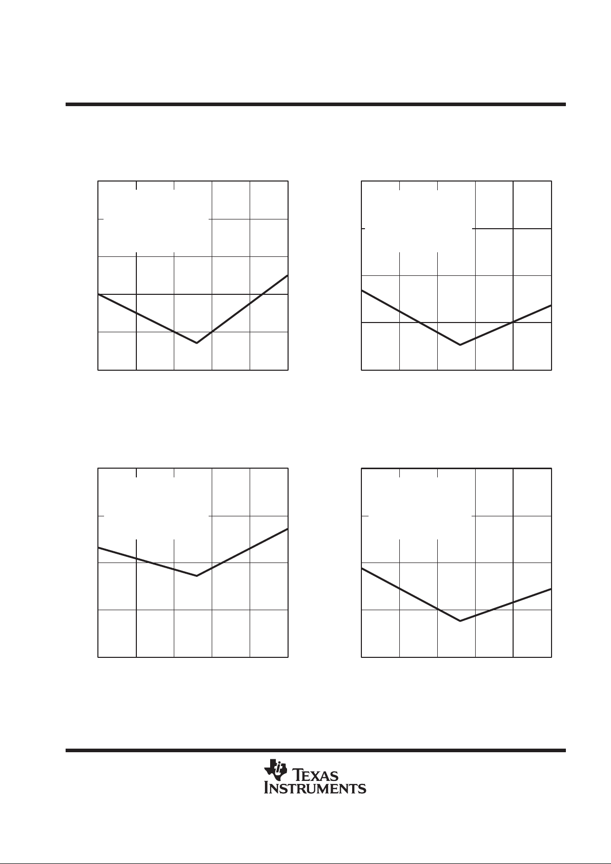
TYPICAL CHARACTERISTICS
Figure 20
0.15
0.16
0.17
0.18
0.19
0.20
–40 –15 10 35 60 85
TA – Temperature – °C
INL – Integral Nonlinearity – LSB
INTEGRAL NONLINEARITY
vs
TEMPERATURE
VCC = 5 V,
Internal Reference = 4 V ,
Internal OSC,
Single Shot,
Short Sample,
Mode 00 µP mode
Figure 21
0.15
0.175
0.200
0.225
0.250
–40 –15 10 35 60 85
TA – Temperature – °C
DNL – Differential Nonlinearity – LSB
DIFFERENTIAL NONLINEARITY
vs
TEMPERATURE
VCC = 5 V,
Internal Reference = 4 V ,
Internal OSC,
Single Shot,
Short Sample,
Mode 00 µP mode
Figure 22
0.15
0.175
0.200
0.225
0.250
–40 –15 10 35 60 85
TA – Temperature – °C
INL – Integral Nonlinearity – LSB
INTEGRAL NONLINEARITY
vs
TEMPERATURE
VCC = 2.7 V,
Internal Reference = 2 V ,
Internal OSC,
Single Shot,
Short Sample,
Mode 00 µP mode
Figure 23
0.2
0.225
0.250
0.275
0.300
–40 –15 10 35 60 85
TA – Temperature – °C
DNL – Differential Nonlinearity – LSB
DIFFERENTIAL NONLINEARITY
vs
TEMPERATURE
VCC = 2.7 V,
Internal Reference = 2 V ,
Internal OSC,
Single Shot,
Short Sample,
Mode 00 µP mode

TLV1504, TLV1508
2.7 V TO 5.5 V, 10-BIT, 200 KSPS, 4/8 CHANNEL, LOW POWER,
SERIAL ANALOG-TO-DIGITAL CONVERTERS WITH AUTO POWER DOWN
SLAS251 – DECEMBER 1999
28
POST OFFICE BOX 655303 • DALLAS, TEXAS 75265
TYPICAL CHARACTERISTICS
Figure 24
0.55
0.575
0.600
0.625
0.650
–40 –15 10 35 60 85
Offset Error – LSB
OFFSET ERROR
vs
TEMPERATURE
TA – Temperature – °C
VCC = 5 V,
External Reference = 4 V ,
External OSC = SCLK/4,
Single Shot,
Short Sample,
Mode 00 µP mode
Figure 25
–0.2
–0.175
–0.150
–0.125
–0.100
–40 –15 10 35 60 85
Gain Error – LSB
GAIN ERROR
vs
TEMPERATURE
TA – Temperature – °C
VCC = 5 V,
External Reference = 4 V ,
ExternalOSC = SCLK/4,
Single Shot,
Short Sample,
Mode 00 µP mode
Figure 26
1
0.8
0.6
–40 25
Supply Current – mA
1.2
SUPPLY CURRENT
vs
TEMPERATURE
1.4
85
TA – Temperature –°C
Long Sample
Short Sample
VCC = 5 V, External Reference = 4 V,
Internal Oscillator, Single Shot,
Short Sample, Mode 00 µP Mode
Figure 27
–0.2
–0.6
–0.8
–1
–40 25
Powerdown Current –
0
0.2
POWER DOWN CURRENT
vs
TEMPERATURE
0.4
85
–0.4
Aµ
TA – Temperature –°C
VCC = 2.7 V
VCC = 5 V
VCC = 5.5 V
External Reference = 4 V , Internal Oscillator,
Single Shot, Short Sample, Mode 00 µP Mode

TLV1504, TLV1508
2.7 V TO 5.5 V, 10-BIT, 200 KSPS, 4/8 CHANNEL, LOW POWER,
SERIAL ANALOG-TO-DIGITAL CONVERTERS WITH AUTO POWER DOWN
SLAS251 – DECEMBER 1999
29
POST OFFICE BOX 655303 • DALLAS, TEXAS 75265
TYPICAL CHARACTERISTICS
–0.3
–0.25
–0.20
–0.15
–0.10
–0.05
–0.00
0.05
0.10
0.15
0.20
0.25
0 512 1024
INL – Integral Nonlinearity – LSB
Samples
INTEGRAL NONLINEARITY
vs
SAMPLES
VCC = 2.7 V, Internal Reference = 2 V, SCLK = 12.5 MHz, Internal Conversion OSC,
Internal Conversion OSC, Single Shot, Short Sample,
Mode 00 DSP Mode
Figure 28
–0.3
–0.2
–0.1
–0.0
0.1
0.2
0.3
0 512 1024
DNL – Differential Nonlinearity – LSB
Samples
DIFFERENTIAL NONLINEARITY
vs
SAMPLES
VCC = 2.7 V, Internal Reference = 2 V, SCLK = 12.5 MHz, Internal Conversion OSC,
Internal Conversion OSC, Single Shot, Short Sample, Mode 00 DSP Mode
Figure 29

TLV1504, TLV1508
2.7 V TO 5.5 V, 10-BIT, 200 KSPS, 4/8 CHANNEL, LOW POWER,
SERIAL ANALOG-TO-DIGITAL CONVERTERS WITH AUTO POWER DOWN
SLAS251 – DECEMBER 1999
30
POST OFFICE BOX 655303 • DALLAS, TEXAS 75265
TYPICAL CHARACTERISTICS
–0.2
–0.15
–0.10
–0.05
–0.00
0.05
0.10
0.15
0.20
0 512 1024
INL – Integral Nonlinearity – LSB
Samples
INTEGRAL NONLINEARITY
vs
SAMPLES
VCC = 5 V, Internal Reference = 4 V, SCLK = 20 MHz, Internal Conversion OSC,
Single Shot, Short Sample, Mode 00 DSP Mode
Figure 30
–0.3
–0.2
–0.1
–0.0
0.1
0.2
0.3
0 512 1024
DNL – Differential Nonlinearity – LSB
Samples
DIFFERENTIAL NONLINEARITY
vs
SAMPLES
VCC = 5 V, Internal Reference = 4 V, SCLK = 20 MHz, Internal Conversion OSC,
Single Shot, Short Sample, Mode 00 DSP Mode
Figure 31

TLV1504, TLV1508
2.7 V TO 5.5 V, 10-BIT, 200 KSPS, 4/8 CHANNEL, LOW POWER,
SERIAL ANALOG-TO-DIGITAL CONVERTERS WITH AUTO POWER DOWN
SLAS251 – DECEMBER 1999
31
POST OFFICE BOX 655303 • DALLAS, TEXAS 75265
TYPICAL CHARACTERISTICS
–140
–120
–100
–80
–60
–40
–20
0
20
0 102030405060708090100
Magnitude – dB
f – Frequency – kHz
FAST FOURIER TRANSFORM
vs
FREQUENCY
VCC = 5 V,
External Reference = 4 V ,
SCLK = 20 MHz,
Internal OSC
Single Shot, Long Sample
Mode 00 µP Mode
Figure 32
–70
–65
–60
–55
–50
0 255075100
Figure 33
SNR – Signal-to-Noise – dB
f – Frequency – kHz
SIGNAL-TO-NOISE
vs
INPUT FREQUENCY
VCC = 5 V, External Reference = 4 V,
Internal OSC, Single Shot, Short Sample,
Mode 00 µP Mode
TLV1504, TLV1508
2.7 V TO 5.5 V, 10-BIT, 200 KSPS, 4/8 CHANNEL, LOW POWER,
SERIAL ANALOG-TO-DIGITAL CONVERTERS WITH AUTO POWER DOWN
SLAS251 – DECEMBER 1999
32
POST OFFICE BOX 655303 • DALLAS, TEXAS 75265
TYPICAL CHARACTERISTICS
–70
–65
–60
–55
–50
0 255075100
Figure 34
SINAD – Signal-to-Noise + Distortion – dB
f – Frequency – kHz
SIGNAL-TO-NOISE + DISTORTION
vs
INPUT FREQUENCY
VCC = 5 V, External Reference = 4 V,
Internal OSC, Single Shot, Short Sample,
Mode 00 µP Mode
7
7.5
8.0
8.5
9.0
9.5
10.0
0 255075100
Figure 35
ENOB – Effective Number of Bits – BITS
f – Frequency – kHz
EFFECTIVE NUMBER OF BITS
vs
INPUT FREQUENCY
VCC = 5 V, External Reference = 4 V,
Internal OSC, Single Shot,
Short Sample, Mode 00 µP Mode
–90
–85
–80
–75
–70
–65
–60
0 255075100
Figure 36
THD – Total Harmonic Distortion – dB
TOTAL HARMONIC DISTORTION
vs
INPUT FREQUENCY
f – Frequency – kHz
VCC = 5 V, External Reference = 4 V,
Internal OSC, Single Shot,
Short Sample, Mode 00 µP Mode
–100
–80
–60
–40
–20
0
0 255075100
Figure 37
Spurious Free Dynamic Range – dB
f – Frequency – kHz
SPURIOUS FREE DYNAMIC RANGE
vs
INPUT FREQUENCY
VCC = 5 V, External Reference = 4 V,
Internal OSC, Single Shot,
Short Sample, Mode 00 µP Mode
TLV1504, TLV1508
2.7 V TO 5.5 V, 10-BIT, 200 KSPS, 4/8 CHANNEL, LOW POWER,
SERIAL ANALOG-TO-DIGITAL CONVERTERS WITH AUTO POWER DOWN
SLAS251 – DECEMBER 1999
33
POST OFFICE BOX 655303 • DALLAS, TEXAS 75265
PRINCIPLES OF OPERATION
1000000000
0111111111
0000000010
0000000001
0000000000
1111111110
0 0.00976 2.4937 2.4986 2.5034
Digital Output Code
1000000001
1111111101
1111111111
4.9874 4.9922 4.9971
512
511
2
1
0
1022
Step
513
1021
1023
0.00244
VI – Analog Input Voltage – V
VZT =VZS + 1/2 LSB
V
ZS
See Notes A and B
4.9898
0.00488
VFT = VFS – 1/2 LSB
V
FS
VFS
Nom
NOTES: A. This curve is based on the assumption that V
ref+
and V
ref–
have been adjusted so that the voltage at the transition from digital 0 to
1 (VZT) is 2.44 mV , and the transition to full scale (VFT) is 4.9898 V , 1 LSB = 4.88 mV.
B. The full scale value (VFS) is the step whose nominal midstep value has the highest absolute value. The zero-scale value (VZS) is
the step whose nominal midstep value equals zero.
Figure 38. Ideal 10-Bit ADC Conversion Characteristics
GND
CS
XF
TMS320 DSP
TLV1504/
TLV1508
SDI
SDO
SCLK
INT
TXD
RXD
CLKR
BIO
10 kΩ
v
cc
A
IN
V
DD
FSR
FS
CLKX
FSX
Figure 39. Typical Interface to a TMS320 DSP
TLV1504, TLV1508
2.7 V TO 5.5 V, 10-BIT, 200 KSPS, 4/8 CHANNEL, LOW POWER,
SERIAL ANALOG-TO-DIGITAL CONVERTERS WITH AUTO POWER DOWN
SLAS251 – DECEMBER 1999
34
POST OFFICE BOX 655303 • DALLAS, TEXAS 75265
PRINCIPLES OF OPERATION
simplified analog input analysis
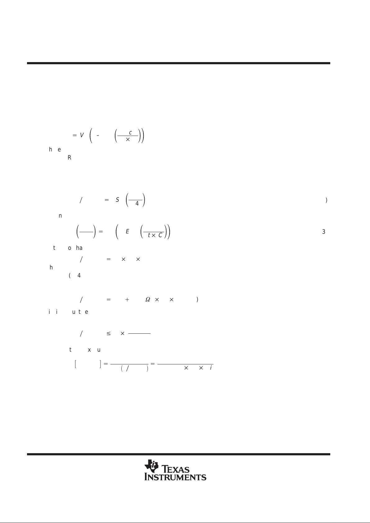
Using the equivalent circuit in Figure 39, the time required to charge the analog input capacitance from 0 to VS
within 1/2 LSB can be derived as follows.
The capacitance charging voltage is given by:
Vc+Vs
ǒ
1
–EXP
ǒ
–tc
Rt Ci
Ǔ
Ǔ
Where
Rt = Rs + Zi
tc = Cycle time
(1)
The input impedance Zi is 0.5 kΩ at 5 V , and is higher (~ 0.6 kΩ) at 2.7 V. The final voltage to 1/2 LSB is given
by:
VC
(1ń2
LSB
)
+
VS–
ǒ
VS
2048
Ǔ
(2)
Equating equation 1 to equation 2 and solving for cycle time tc gives:
Vs–
ǒ
VS
2048
Ǔ
+
Vs
ǒ
1
–EXP
ǒ
–tc
Rt Ci
Ǔ
Ǔ
(3)
and time to change to 1/2 LSB (minimum sampling time) is:
tch
(1ń2
LSB
)
+Rt Ci In(2048)
Where
In(2048) = 7.625
Therefore, with the values given, the time for the analog input signal to settle is:
tch
(1ń2
LSB
)
+
(
Rs
)
0.5kW) Ci In(2048)
(4)
This time must be less than the converter sample time shown in the timing diagrams. This is 12× SCLKs (if the
sampling mode is short normal sampling mode).
tch
(1ń2
LSB
)v12
1
f(SCLK
)
(5)
Therefore the maximum SCLK frequency is:
maxƪf(SCLK
)
ƫ
+
12
tch
ǒ
1ń2
LSB
Ǔ
+
12
[
In
(
2048) Rt
Ci
]
(6)
TLV1504, TLV1508
2.7 V TO 5.5 V, 10-BIT, 200 KSPS, 4/8 CHANNEL, LOW POWER,
SERIAL ANALOG-TO-DIGITAL CONVERTERS WITH AUTO POWER DOWN
SLAS251 – DECEMBER 1999
35
POST OFFICE BOX 655303 • DALLAS, TEXAS 75265
PRINCIPLES OF OPERATION
R
s
r
i
V
S
V
C
Driving Source
†
TLV1504/08
C
i
V
I
VI= Input Voltage at AIN
VS= External Driving Source Voltage
Rs= Source Resistance
ri= Input Resistance (MUX on Resistance)
Ci= Input Capacitance
VC= Capacitance Charging Voltage
†
Driving source requirements:
• Noise and distortion for the source must be equivalent to the resolution of the converter.
• Rs must be real at the input frequency.
Figure 40. Equivalent Input Circuit Including the Driving Source
maximum conversion throughput
For a supply voltage of 5 V, if the source impedance is less than 1 kΩ, and the ADC analog input capacitance
Ci is less than 50 pF, this equates to a minimum sampling time tch(0.5 LSB) of 0.571 µs (t1µs). Since the
sampling time requires 12 SCLKs, the fastest SCLK frequency is 12/tch = 12 MHz.
The minimal total cycle time is given as:
tc+tcommand)tch)tconv)td(EOCH–CSL
)
+4
1
f(SCLK
)
)12
1
f(SCLK
)
)
3.25
ms)
0.1
m
s
+16
1
12
MHz
)
3.35
ms+
4.68
m
s
This is equivalent to a maximum throughput of ~200 KSPS. The throughput can be even higher with a smaller
source impedance.
When source impedance is 100 Ω, the minimum sampling time becomes:
tch
(1ń2
LSB
)
+Rt Ci In(2048)+0.23
m
s
The maximum SCLK frequency possible is 12/tch = 52 MHz. Then a 20 MHz clock (maximum SCLK frequency
for the TLV1504/1508 ) can be used. The minimal total cycle time is then reduced to:
tc+tcommand)tch)tconv)td(EOCH–CSL
)
+4
1
f(SCLK
)
)12
1
f(SCLK
)
)
3.25
ms)
0.1
m
s
+
0.8
ms)
3.35
ms+
4.15
m
s
The maximum throughput is 1/4.15 µs ~ 240 KSPS for this case.

TLV1504, TLV1508
2.7 V TO 5.5 V, 10-BIT, 200 KSPS, 4/8 CHANNEL, LOW POWER,
SERIAL ANALOG-TO-DIGITAL CONVERTERS WITH AUTO POWER DOWN
SLAS251 – DECEMBER 1999
36
POST OFFICE BOX 655303 • DALLAS, TEXAS 75265
PRINCIPLES OF OPERATION
400
300
200
5.5 5 4.5 4
MUX ON Resistance –
500
600
700
3.5 3 2.7
VCC – Supply Voltage – V
Ω
Figure 41. Input MUX Impedance vs Supply Voltage
power down calculations
i(AVERAGE) = (fS/f
SMAX
) × i(ON) + (1–fS/f
SMAX
) × i(OFF)
CASE 1: If VDD = 3.3 V, auto power down, and an external reference is used:
f
S
+
10
kHz
f
SMAX
+
200
kHz
i(ON
)
+X
1
mA operating current and i(OFF
)
+X1m
A auto powerdown current
so
i(AVERAGE
)+0.05 1000
mA)
0.95 1
mA+51m
A
CASE 2: Now if software power down is used, another cycle is needed to shut it down.
f
S
+
20
kHz
f
SMAX
+
200
kHz
i
(ON)
+X
1
mA operating current and i(OFF
)
+X1m
A powerdown current
so
i(AVERAGE
)+0.1 1000
mA)
0.9 1
mA+
101
m
A
In reality this will be less since the second conversion never happened. It is only the additional cycle to shut down
the ADC.

TLV1504, TLV1508
2.7 V TO 5.5 V, 10-BIT, 200 KSPS, 4/8 CHANNEL, LOW POWER,
SERIAL ANALOG-TO-DIGITAL CONVERTERS WITH AUTO POWER DOWN
SLAS251 – DECEMBER 1999
37
POST OFFICE BOX 655303 • DALLAS, TEXAS 75265
PRINCIPLES OF OPERATION
CASE 3: Now if the hardware power down is used.
f
S
+
10
kHz
f
SMAX
+
200
kHz
i(ON
)
+X
1
mA operating current and i(OFF
)
+X1m
A powerdown current
so
i(AVERAGE
)+0.05 1000
mA)
0.95 1
mA+51m
A
difference between modes of conversion
The major difference between sweep mode (mode 10) and repeat sweep mode (mode 11) is that the sweep
sequence ends after the FIFO is filled up to the programmed threshold. The repeat sweep can either dump the
FIFO (by ignoring the FIFO content but simply reconfiguring the device) or read the FIFO and then repeat the
conversions on the the same sequence of the channel as before.
FIFO reads are expected after the FIFO is filled up to the threshold in each case. Mode 10 – the device allows
only FIFO read or CFR read or CFR write to be executed. Any conversion command is ignored. In the case of
mode 1 1, in addition to the above commands, conversion commands are also executed , i.e. the FIFO is cleared
and the sweep sequence is restarted.
Both single shot and repeat modes require selection of a channel after the device is configured for these modes.
Single shot mode does not use the FIFO, but repeat mode does. When the device is operating in repeat mode,
the FIFO can be dumped (by ignoring the FIFO content and simply reconfiguring the device) or the FIFO can
be read and then the conversions repeated on the same channel as before. However, the channel has to be
selected first before any conversion can be carried out. The devices can be programmed with the following
sequences for operating in the different modes that use a FIFO:

TLV1504, TLV1508
2.7 V TO 5.5 V, 10-BIT, 200 KSPS, 4/8 CHANNEL, LOW POWER,
SERIAL ANALOG-TO-DIGITAL CONVERTERS WITH AUTO POWER DOWN
SLAS251 – DECEMBER 1999
38
POST OFFICE BOX 655303 • DALLAS, TEXAS 75265
PRINCIPLES OF OPERATION
difference between modes of conversion (continued)
REPEAT:
Configure FIFO Depth=4 /CONV Mode 01
Select Channel/
1st Conv (CS or CSTART)
2nd Conv (CS
or CSTART)
3rd Conv (CS or CSTART)
4th Conv (CS or CSTART
FIFO READ 1
FIFO READ 2
FIFO READ 3
FIFO READ 4
Select Channel
1st Conv (CS
or CSTART)
2nd Conv (CS or CSTART)
3rd Conv (CS
or CSTART)
4th Conv (CS or CSTART
SWEEP:
Configure FIFO Depth=4 SEQ=1–2–3–4/CONV Mode 10
conv ch 1 (CS
/CSTART)
conv ch 2 (CS/CSTART)
conv ch 3 (CS/CSTART)
conv ch 4 (CS/CSTART
FIFO READ ch 1 result
FIFO READ ch 2 result
FIFO READ ch 3 result
FIFO READ ch 4 result
Configure (not required if same sweep sequence is to be used again)
REPEAT SWEEP:
Configure FIFO Depth=4 SWEEP SEQ=1-2-3-4/CONV Mode 1 1
conv ch 1 (CS
/CSTART)
conv ch 2 (CS/CSTART)
conv ch 3 (CS/CSTART)
conv ch 4 (CS/CSTART
FIFO READ ch 1 result
FIFO READ ch 2 result
FIFO READ ch 3 result
FIFO READ ch 4 result
conv ch 1 (CS
/CSTART)
conv ch 2 (CS/CSTART)
conv ch 3 (CS
/CSTART)
conv ch 4 (CS/CSTART
TLV1504, TLV1508
2.7 V TO 5.5 V, 10-BIT, 200 KSPS, 4/8 CHANNEL, LOW POWER,
SERIAL ANALOG-TO-DIGITAL CONVERTERS WITH AUTO POWER DOWN
SLAS251 – DECEMBER 1999
39
POST OFFICE BOX 655303 • DALLAS, TEXAS 75265
MECHANICAL DATA
D (R-PDSO-G**) PLASTIC SMALL-OUTLINE PACKAGE
14 PINS SHOWN
4040047/D 10/96
0.228 (5,80)
0.244 (6,20)
0.069 (1,75) MAX
0.010 (0,25)
0.004 (0,10)
1
14
0.014 (0,35)
0.020 (0,51)
A
0.157 (4,00)
0.150 (3,81)
7
8
0.044 (1,12)
0.016 (0,40)
Seating Plane
0.010 (0,25)
PINS **
0.008 (0,20) NOM
A MIN
A MAX
DIM
Gage Plane
0.189
(4,80)
(5,00)
0.197
8
(8,55)
(8,75)
0.337
14
0.344
(9,80)
16
0.394
(10,00)
0.386
0.004 (0,10)
M
0.010 (0,25)
0.050 (1,27)
0°–8°
NOTES: A. All linear dimensions are in inches (millimeters).
B. This drawing is subject to change without notice.
C. Body dimensions do not include mold flash or protrusion, not to exceed 0.006 (0,15).
D. Falls within JEDEC MS-012
TLV1504, TLV1508
2.7 V TO 5.5 V, 10-BIT, 200 KSPS, 4/8 CHANNEL, LOW POWER,
SERIAL ANALOG-TO-DIGITAL CONVERTERS WITH AUTO POWER DOWN
SLAS251 – DECEMBER 1999
40
POST OFFICE BOX 655303 • DALLAS, TEXAS 75265
MECHANICAL DATA
DW (R-PDSO-G**) PLASTIC SMALL-OUTLINE PACKAGE
16 PINS SHOWN
4040000/C 07/96
Seating Plane
0.400 (10,15)
0.419 (10,65)
0.104 (2,65) MAX
1
0.012 (0,30)
0.004 (0,10)
A
8
16
0.020 (0,51)
0.014 (0,35)
0.293 (7,45)
0.299 (7,59)
9
0.010 (0,25)
0.050 (1,27)
0.016 (0,40)
(15,24)
(15,49)
PINS **
0.010 (0,25) NOM
A MAX
DIM
A MIN
Gage Plane
20
0.500
(12,70)
(12,95)
0.510
(10,16)
(10,41)
0.400
0.410
16
0.600
24
0.610
(17,78)
28
0.700
(18,03)
0.710
0.004 (0,10)
M
0.010 (0,25)
0.050 (1,27)
0°–8°
NOTES: A. All linear dimensions are in inches (millimeters).
B. This drawing is subject to change without notice.
C. Body dimensions do not include mold flash or protrusion not to exceed 0.006 (0,15).
D. Falls within JEDEC MS-013
TLV1504, TLV1508
2.7 V TO 5.5 V, 10-BIT, 200 KSPS, 4/8 CHANNEL, LOW POWER,
SERIAL ANALOG-TO-DIGITAL CONVERTERS WITH AUTO POWER DOWN
SLAS251 – DECEMBER 1999
41
POST OFFICE BOX 655303 • DALLAS, TEXAS 75265
MECHANICAL DATA
PW (R-PDSO-G**) PLASTIC SMALL-OUTLINE PACKAGE
14 PINS SHOWN
0,65
M
0,10
0,10
0,25
0,50
0,75
0,15 NOM
Gage Plane
28
9,80
9,60
24
7,90
7,70
2016
6,60
6,40
4040064/F 01/97
0,30
6,60
6,20
8
0,19
4,30
4,50
7
0,15
14
A
1
1,20 MAX
14
5,10
4,90
8
3,10
2,90
A MAX
A MIN
DIM
PINS **
0,05
4,90
5,10
Seating Plane
0°–8°
NOTES: A. All linear dimensions are in millimeters.
B. This drawing is subject to change without notice.
C. Body dimensions do not include mold flash or protrusion not to exceed 0,15.
D. Falls within JEDEC MO-153

IMPORTANT NOTICE
T exas Instruments and its subsidiaries (TI) reserve the right to make changes to their products or to discontinue
any product or service without notice, and advise customers to obtain the latest version of relevant information
to verify, before placing orders, that information being relied on is current and complete. All products are sold
subject to the terms and conditions of sale supplied at the time of order acknowledgement, including those
pertaining to warranty, patent infringement, and limitation of liability.
TI warrants performance of its semiconductor products to the specifications applicable at the time of sale in
accordance with TI’s standard warranty. Testing and other quality control techniques are utilized to the extent
TI deems necessary to support this warranty. Specific testing of all parameters of each device is not necessarily
performed, except those mandated by government requirements.
CERT AIN APPLICATIONS USING SEMICONDUCTOR PRODUCTS MAY INVOLVE POTENTIAL RISKS OF
DEATH, PERSONAL INJURY, OR SEVERE PROPERTY OR ENVIRONMENTAL DAMAGE (“CRITICAL
APPLICATIONS”). TI SEMICONDUCTOR PRODUCTS ARE NOT DESIGNED, AUTHORIZED, OR
WARRANTED TO BE SUITABLE FOR USE IN LIFE-SUPPORT DEVICES OR SYSTEMS OR OTHER
CRITICAL APPLICATIONS. INCLUSION OF TI PRODUCTS IN SUCH APPLICA TIONS IS UNDERSTOOD T O
BE FULLY AT THE CUSTOMER’S RISK.
In order to minimize risks associated with the customer’s applications, adequate design and operating
safeguards must be provided by the customer to minimize inherent or procedural hazards.
TI assumes no liability for applications assistance or customer product design. TI does not warrant or represent
that any license, either express or implied, is granted under any patent right, copyright, mask work right, or other
intellectual property right of TI covering or relating to any combination, machine, or process in which such
semiconductor products or services might be or are used. TI’s publication of information regarding any third
party’s products or services does not constitute TI’s approval, warranty or endorsement thereof.
Copyright 1999, Texas Instruments Incorporated
 Loading...