

TLS1233
VIDEO PREAMPLIFIER SYSTEM
SLVS126C – JULY 1995 – REVISED JUNE 1996
V
CC1
GND
N PACKAGE
(TOP VIEW)
1
20
2
19
3
18
4
17
5
16
6
15
7
14
8
13
9
12
10
11
G CLAMP(+)
B CLAMP(+)
R VIDEO OUT
R GAIN ADJUST
V
CC2
G VIDEO OUT
G GAIN ADJUST
B VIDEO OUT
B GAIN ADJUST
CLAMP GATE
D
Wide Bandwidth...Typ 100 MHz at –3 dB
D
Three Channels
D
0 V to 4 V, Digital Level-Contrast Control
D
0 V to 4 V, Digital Level-Gain Adjust Control
D
20-Pin Plastic DIP for Small PCB Area
Required
D
Fewer Peripheral Components Required
Than for LM1203 Applications
D
Independent CLAMP(+) Adjustment to Each
Channel
description
R CLAMP(+)
R VIDEO IN
R CLAMP CAP
G VIDEO IN
G CLAMP CAP
B VIDEO IN
B CLAMP CAP
CONTRAST
The TLS1233 is a 100-MHz wide-band video preamplifier system intended for mid-to-high-resolution RGB
(red-green-blue) color monitors. Each video amplifier (R, G, and B) contains a gain set for adjusting maximum
system gain (A
= 7.8 V/V). The TLS1233 provides digital level-operated contrast, brightness, and gain
V
adjustment control. All the control inputs offer high input impedance and an operation range from 0 V to 4 V for
easy interface to the serial digital buses. Provided in a 20-pin plastic dual-in-line package (DIP), the TLS1233
integrates most of the external components required to accommodate the video system.
The TLS1233 operates from a 12-V supply and contains an internal input bias voltage. Also, the TLS1233
contains the feedback resistor required between output and CLAMP(–) for dc level holding. The device is
characterized for operation from 0°C to 70°C.
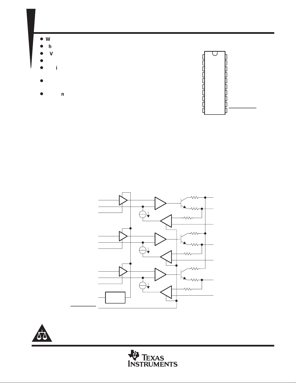
functional block diagram
R VIDEO IN
R CLAMP CAP
R GAIN ADJUST
G VIDEO IN
G CLAMP CAP
G GAIN ADJUST
B VIDEO IN
B CLAMP CAP
B GAIN ADJUST
CONTRAST
CLAMP GATE
3
4
17
5
7
14
8
9
12
10
11
Contrast
Control
A1
A1
A1
A2
A2
A2
16
V
CC2
18
R VIDEO OUT
1
R CLAMP(+)
15
G VIDEO OUT
20
G CLAMP(+)
13
B VIDEO OUT
19
B CLAMP(+)
Please be aware that an important notice concerning availability, standard warranty, and use in critical applications of
Texas Instruments semiconductor products and disclaimers thereto appears at the end of this data sheet.
PRODUCTION DATA information is current as of publication date.
Products conform to specifications per the terms of Texas Instruments
standard warranty. Production processing does not necessarily include
testing of all parameters.
POST OFFICE BOX 655303 • DALLAS, TEXAS 75265
Copyright 1996, Texas Instruments Incorporated
1
TLS1233
VIDEO PREAMPLIFIER SYSTEM
SLVS126C – JULY 1995 – REVISED JUNE 1996
TLS1233Y chip information
This chip, when properly assembled, displays characteristics similar to the TLS1233. Thermal compression or
ultrasonic bonding may be used on the doped-aluminum bonding pads. The chips may be mounted with
conductive epoxy or a gold-silicon preform.
BONDING PAD ASSIGNMENTS
2 1 20 19
8
78
18
17
16
15
14
131211109
CHIP THICKNESS: 15 TYPICAL
BONDING PADS: 4 × 4 MINIMUM
TJ max = 150°C
TOLERANCES ARE ±10%.
ALL DIMENSIONS ARE IN MILS.
76
3
4
5
6
6
7
absolute maximum ratings over operating free-air temperature range (unless otherwise noted)
Supply voltage, V
Input voltage range, V
Video output current, I
Total power dissipation at (or below) 25°C free-air temperature (see Note 2) 1.87 W. . . . . . . . . . . . . . . . . . . .
Operating virtual junction temperature range, T
Operating free-air temperature range, T
Storage temperature range, T
Lead temperature 1,6 mm (1/16 inch) from case for 10 seconds 260°C. . . . . . . . . . . . . . . . . . . . . . . . . . . . . . .
†
Stresses beyond those listed under “absolute maximum ratings” may cause permanent damage to the device. These are stress ratings only, and
functional operation of the device at these or any other conditions beyond those indicated under “recommended operating conditions” is not
implied. Exposure to absolute-maximum-rated conditions for extended periods may affect device reliability.
NOTES: 1. All VCC terminals must be externally wired together to prevent internal damage during VCC power-on/-off cycles.
2. For operation above 25°C free-air temperature, derate linearly from 1.87 W (TA = 25°C) to 1.2 W (TA = 70°C). This equates to a
derating factor of 15 mW/°C.
13.5 V. . . . . . . . . . . . . . . . . . . . . . . . . . . . . . . . . . . . . . . . . . . . . . . . . . . . . . . . . . . . . . . . . . . . .
CC
(see Note 1) 0 V to V
I
(per channel) 28 mA. . . . . . . . . . . . . . . . . . . . . . . . . . . . . . . . . . . . . . . . . . . . . . . . . . . . . .
O
stg
. . . . . . . . . . . . . . . . . . . . . . . . . . . . . . . . . . . . . . . . . . . . . . . . . . . .
–55°C to 150°C. . . . . . . . . . . . . . . . . . . . . . . . . . . . . . . . . . . .
J
0°C to 70°C. . . . . . . . . . . . . . . . . . . . . . . . . . . . . . . . . . . . . . . . . . . . . .
A
–65°C to 150°C. . . . . . . . . . . . . . . . . . . . . . . . . . . . . . . . . . . . . . . . . . . . . . . . . .
†
CC
2
POST OFFICE BOX 655303 • DALLAS, TEXAS 75265
Crosstalk attenuation
a
()
TLS1233
VIDEO PREAMPLIFIER SYSTEM
SLVS126C – JULY 1995 – REVISED JUNE 1996
recommended operating conditions
MIN NOM MAX UNIT
Supply voltage, V
High-level input voltage range, CLAMP GATE, V
Low-level input voltage range, CLAMP GATE, V
Operating free-air temperature, T
electrical characteristics at 25°C free-air temperature range, CLAMP GA TE = 0 V, CLAMP(+) = 2 V,
CONTRAST = R,G,B GAIN ADJUST = 4 V , V
I
CC
V
ref
I
I
I
IL
I
IH
V
OL
V
OH
V
O(diff)
Supply current
Video input reference voltage Measure R/G/B video input 2.1 2.3 2.5 V
Contrast and R,G,B GAIN ADJUST
input current
Clamp gate low input current CLAMP GATE = 0 V –0.5 –2.4 µA
Clamp gate high input current CLAMP GATE = 12 V 0.005 1 µA
Clamp capacitor charge current I
Clamp capacitor discharge current I
Low-level output voltage R,G,B CLAMP CAP = 0 V 0.3 V
High-level output voltage R,G,B CLAMP CAP = 5 V 7.8 V
Output voltage difference V
and V
CC1
PARAMETER
CC2
11 12 13 V
IH
IL
A
CC1
ALTERNA TE
SYMBOL
K(chg)
K(dschg)
O(diff)
Clamp comparators off 2.4 5 V
Clamp comparators on 0 0.8 V
0 70 °C
=V
= 12 V (see Figure 2) (unless otherwise noted)
CC2
TEST CONDITIONS MIN TYP MAX
V
+ V
CC1
Measure CONTRAST,
R/G/B GAIN ADJUST
R,G,B CLAMP CAP = 0 V 1 mA
R,G,B CLAMP CAP = 5 V –1 mA
Between any two channels ±0.5 ±50 mV
CC2
84 94 mA
–0.5 -10 µA
UNIT
operating characteristics at 25°C free-air temperature, CLAMP GATE = 0 V, CLAMP(+) = 4 V,
= 10 kHz, V
CONTRAST = R,G,B GAIN ADJUST = 4 V , f
PARAMETER
A
V(max)
A
V(mid)
THD Total harmonic distortion CONTRAST = 1 V, V
BW Amplifier bandwidth BW(–3 dB)
NOTES: 3. Determine V
Maximum voltage amplification A
Midrange voltage amplification A
Contrast voltage for minimum
amplification
Amplification match at A
Amplification match at A
Amplification match at A
Pulse test for rise time t
Pulse test for fall time t
4. Measure gain difference between any two amplifiers, V
5. Adjust input frequency from 10 kHz (A
6. V
I(PP)
7. A special text fixture without a socket and a double-sided full-ground-plane PC board are required.
CONT-LOW
= 700 mV at f = 10 kHz to any amplifier. Measure output levels of the other two undriven amplifiers relative to driven amplifier.
V(max)AVmax(diff)
V(mid)AVmid(diff)
V(low)
for –40 dB attenuation of output. Reference to A
ALTERNATE
SYMBOL
VMAX
VMID
V
CONT-LOWVI(PP)
A
Vlow(diff)
x
r
f
V(max)
I
TEST CONDITIONS MIN TYP MAX UNIT
CONTRAST = 4 V, V
CONTRAST = 2 V, V
= 1 V, See Note 3 1 V
CONTRAST = 4 V, See Note 4 ±0.2 dB
CONTRAST = 2 V, See Note 3 ±0.2 dB
CONTRAST = V
See Note 3 and 4
CONTRAST = 4 V,
See Notes 5 And 7
CONTRAST = 4 V,
See Note 6
CONTRAST = 4 V,
f = 10 MHz,
CONTRAST = 4 V, CLAMP(+) = 2 V,
V
= 4 V
O(PP)
= 1 V.
reference level) to the –3-dB corner frequency (f –3 dB). V
I(PP)
= V
CC1
IPP
IPP
CONT-LOW
IPP
f = 10 kHz,
See Notes 6 or 7
See Notes 5 and 7
V(max)
= 12 V (unless otherwise noted)
CC2
= 700 mV 7.8 V/V
= 700 mV 2 V/V
,
= 1 V 0.5 %
.
±0.2 dB
100 MHz
60 dB
40 dB
3 ns
4 ns
= 700 mV.
I(PP)
POST OFFICE BOX 655303 • DALLAS, TEXAS 75265
3

TLS1233
VIDEO PREAMPLIFIER SYSTEM
SLVS126C – JULY 1995 – REVISED JUNE 1996
PARAMETER MEASUREMENT INFORMATION
CLAMP(+)
12 V
R Video In
G Video In
10 µF
75 Ω
75 Ω
0.1 µF
+
0.1 µF
0.1 µF
0.1 µF
10 µF
0.1 µF
10 µF
0.1 µF
1
R CLAMP(+)
2
V
CC1
3
+
+
R VIDEO IN
4
R CLAMP CAP
5
G VIDEO IN
6
GND
7
G CLAMP CAP
G CLAMP(+)
B CLAMP(+)
R VIDEO OUT
R GAIN ADJUST
V
G VIDEO OUT
G GAIN ADJUST
CC2
20
19
18
17
16
0.1 µF
15
14
390 Ω
0.1 µF
390 Ω
0.1 µF
To Red
Cascade Driver
0 V to 4 V
12 V
+
10 µF
To Green
Cascade Driver
0 V to 4 V
B Video In
CONTRAST
75 Ω
0.1 µF
+
10 µF
0.1 µF
0.1 µF
8
B VIDEO IN
9
B CLAMP CAP
10
CONTRAST
Figure 1. Test Circuit
B VIDEO OUT
B GAIN ADJUST
CLAMP GATE
13
12
11
390 Ω
0.1 µF
To Blue
Cascade Driver
0 V to 4 V
CLAMP GATE
4
POST OFFICE BOX 655303 • DALLAS, TEXAS 75265

TLS1233
VIDEO PREAMPLIFIER SYSTEM
SLVS126C – JULY 1995 – REVISED JUNE 1996
APPLICATION INFORMATION
12 V
R Video In
G Video In
4 V
10 µF
75 Ω
75 Ω
0.1 µF
+
0.1 µF
0.1 µF
10 µF
0.1 µF
0.1 µF
10 µF
0.1 µF
4 V
1
R CLAMP(+)
2
V
CC1
3
+
+
R VIDEO IN
4
R CLAMP CAP
5
G VIDEO IN
6
GND
7
G CLAMP CAP
G CLAMP(+)
B CLAMP(+)
R VIDEO OUT
R GAIN ADJUST
G VIDEO OUT
G GAIN ADJUST
V
CC2
20
19
18
17
16
0.1 µF
15
14
390 Ω
0.1 µF
390 Ω
0.1 µF
4 V
To Red
Cascade Driver
4 V
12 V
+
10 µF
To Green
Cascade Driver
4 V
0.1 µF
B Video In
75 Ω
4 V
CONTRAST
0.1 µF
†
Minimum pulse width: 300 ns
+
10 µF
0.1 µF
8
B VIDEO IN
9
B CLAMP CAP
10
CONTRAST
B VIDEO OUT
B GAIN ADJUST
CLAMP GATE
Figure 2. Application Circuit
13
12
11
To Blue
390 Ω
0.1 µF
100 Ω100 Ω
Cascade Driver
4 V
CLAMP GATE
†
POST OFFICE BOX 655303 • DALLAS, TEXAS 75265
5

TLS1233
VIDEO PREAMPLIFIER SYSTEM
SLVS126C – JULY 1995 – REVISED JUNE 1996
MECHANICAL DATA
N (R-PDIP-T**) PLASTIC DUAL-IN-LINE PACKAGE
16 PIN SHOWN
16
1
0.035 (0,89) MAX
PINS **
DIM
A
9
0.260 (6,60)
0.240 (6,10)
8
0.070 (1,78) MAX
0.020 (0,51) MIN
0.200 (5,08) MAX
A MAX
A MIN
Seating Plane
14
0.775
(19,69)
0.745
(18,92)
16
0.775
(19,69)
0.745
(18,92)
18
0.920
(23.37)
0.850
(21.59)
20
0.975
(24,77)
0.940
(23,88)
0.310 (7,87)
0.290 (7,37)
0.100 (2,54)
0.021 (0,53)
0.015 (0,38)
NOTES: A. All linear dimensions are in inches (millimeters).
B. This drawing is subject to change without notice.
C. Falls within JEDEC MS-001 (20 pin package is shorter then MS-001.)
0.010 (0,25)
M
0.125 (3,18) MIN
0°–15°
0.010 (0,25) NOM
14/18 PIN ONL Y
4040049/C 08/95
6
POST OFFICE BOX 655303 • DALLAS, TEXAS 75265

IMPORTANT NOTICE
T exas Instruments and its subsidiaries (TI) reserve the right to make changes to their products or to discontinue
any product or service without notice, and advise customers to obtain the latest version of relevant information
to verify, before placing orders, that information being relied on is current and complete. All products are sold
subject to the terms and conditions of sale supplied at the time of order acknowledgement, including those
pertaining to warranty, patent infringement, and limitation of liability.
TI warrants performance of its semiconductor products to the specifications applicable at the time of sale in
accordance with TI’s standard warranty. Testing and other quality control techniques are utilized to the extent
TI deems necessary to support this warranty . Specific testing of all parameters of each device is not necessarily
performed, except those mandated by government requirements.
CERT AIN APPLICATIONS USING SEMICONDUCTOR PRODUCTS MAY INVOLVE POTENTIAL RISKS OF
DEATH, PERSONAL INJURY, OR SEVERE PROPERTY OR ENVIRONMENTAL DAMAGE (“CRITICAL
APPLICATIONS”). TI SEMICONDUCTOR PRODUCTS ARE NOT DESIGNED, AUTHORIZED, OR
WARRANTED TO BE SUITABLE FOR USE IN LIFE-SUPPORT DEVICES OR SYSTEMS OR OTHER
CRITICAL APPLICA TIONS. INCLUSION OF TI PRODUCTS IN SUCH APPLICATIONS IS UNDERST OOD TO
BE FULLY AT THE CUSTOMER’S RISK.
In order to minimize risks associated with the customer’s applications, adequate design and operating
safeguards must be provided by the customer to minimize inherent or procedural hazards.
TI assumes no liability for applications assistance or customer product design. TI does not warrant or represent
that any license, either express or implied, is granted under any patent right, copyright, mask work right, or other
intellectual property right of TI covering or relating to any combination, machine, or process in which such
semiconductor products or services might be or are used. TI’s publication of information regarding any third
party’s products or services does not constitute TI’s approval, warranty or endorsement thereof.
Copyright 1998, Texas Instruments Incorporated
 Loading...