

Page 1
User's Guide
SLLU132–October 2010
TLK6002 Dual-Channel, 0.47-Gbps to 6.25-Gbps,
Multi-Rate Transceiver Evaluation Module
This user’s guide describes the usage and construction of the TLK6002 evaluation module (EVM). This
document provides guidance on proper use of the EVM by showing some device configurations and test
modes. In addition, design, layout, and schematic information is provided to the user. Users can use
information in this guide to choose the optimal design methods and materials when designing a complete
system.
WARNING
This equipment is intended for use in a laboratory test environment
only. It generates, uses, and can radiate radio frequency energy
and has not been tested for compliance with the limits of
computing devices pursuant to subpart J of part 15 of FCC rules,
which are designed to provide reasonable protection against radio
frequency interference. Operation of this equipment in other
environments may cause interference with radio communications,
in which case, users at their expense are required to take whatever
measures may be required to correct this interference.
Contents
1 Introduction .................................................................................................................. 4
2 EVM PCB and High-Speed Design Considerations .................................................................... 5
3 TLK6002 EVM Kit Contents ............................................................................................... 6
4 Power ......................................................................................................................... 6
5 Power Monitoring LEDs .................................................................................................... 9
6 Control and Output Status Signals ...................................................................................... 11
6.1 Control Signal and Status Pin Descriptions: .................................................................. 11
7 PRBS PASS Latch Circuits .............................................................................................. 16
8 MDIO ........................................................................................................................ 18
9 JTAG ........................................................................................................................ 19
10 Reset ........................................................................................................................ 20
11 Parallel Signals ............................................................................................................ 21
12 Peripheral Ports ............................................................................................................ 23
13 Test and Setup Configurations .......................................................................................... 24
14 TLK6002EVM Schematics ............................................................................................... 26
15 TLK6002EVM Bill of Materials ........................................................................................... 54
16 TLK6002EVM Board Layouts ............................................................................................ 60
List of Figures
1 TLK6002 EVM Power Source Selection Example ..................................................................... 6
2 TLK6002 EVM 1p5/8V Voltage Source Selection ...................................................................... 7
3 TLK6002 EVM Regulator Voltage Margin Selection ................................................................... 7
4 TLK6002 EVM Global Regulator Margin Selection..................................................................... 8
SLLU132–October 2010 TLK6002 Dual-Channel, 0.47-Gbps to 6.25-Gbps, Multi-Rate Transceiver
Submit Documentation Feedback
Evaluation Module
1
Copyright © 2010, Texas Instruments Incorporated
Page 2

www.ti.com
5 TLK6002 EVM Voltage Monitor LED Enabled Example............................................................... 9
6 TLK6002 EVM Voltage Monitor LED Disabled Example............................................................. 10
7 TLK6002 EVM Voltage Monitor LED Connected Directly to Plane Example...................................... 10
8 Control Connectors (JMP17, JMP23, JMP26, JMP27, JMP29, JMP33, JMP43) ................................ 11
9 TLK6002 EVM MDIO Connector (JMP30) ............................................................................. 17
10 TLK6002 EVM MDIO Connector (JMP30) ............................................................................. 18
11 TLK6002 EVM JTAG Connector (JMP35) ............................................................................. 19
12 RESET Switch – SW1, JMP14, or JMP15............................................................................. 20
13 Parallel Signal Header Block Diagram.................................................................................. 21
14 Parallel Loopback Example .............................................................................................. 22
15 TDA[19:0] Static Clock Data Pattern Example ........................................................................ 23
16 Example TLK6002EVM Test Configuration – Serial Loopback ..................................................... 24
17 Example TLK6002 EVM Test Configuration – Parallel Loopback................................................... 25
18 Cover Page and Index, Sheet 1 ........................................................................................ 26
19 Device Power and Ground, Sheet 2 .................................................................................... 27
20 Global Signals, Sheet 3................................................................................................... 28
21 High-Speed Differential, Sheet 4........................................................................................ 29
22 Reference and Output Clocks, Sheet 5 ................................................................................ 30
23 JTAG, SPI, I2C, STCI, and MDIO, Sheet 6............................................................................ 31
24 TD and RD Parallel Data Lines, Sheet 7............................................................................... 32
25 TX/RX Clocks and A and B Control, Sheet 8.......................................................................... 33
26 PRBS Pass/Fail LEDs, Sheet 9 ......................................................................................... 34
27 1p0V Power Regulator, Sheet 10 ....................................................................................... 35
28 1p2V Power Regulator, Sheet 11 ....................................................................................... 36
29 1p5V Power Regulator, Sheet 12 ....................................................................................... 37
30 1p8V Power Regulator, Sheet 13 ....................................................................................... 38
31 2p5V Power Regulator, Sheet 14 ....................................................................................... 39
32 3p3V Power Regulator, Sheet 15 ....................................................................................... 40
33 Power Regulator Min/Nom/Max Adjustment, Sheet 16............................................................... 41
34 Power Regulator Min/Nom/Max Adjustment LEDs, Sheet 17 ....................................................... 42
35 Power Distribution, Sheet 18............................................................................................. 43
36 1p0V and 1p2V Supply LEDs, Sheet 19 ............................................................................... 44
37 1p5V and 1p8V Supply LEDs, Sheet 20 ............................................................................... 45
38 2p5V, 3p3V, and 5V Supply LEDs, Sheet 21.......................................................................... 46
39 DVDD Supply LEDs, Sheet 22 .......................................................................................... 47
40 1p5/8V Supply LEDs, Sheet 23.......................................................................................... 48
41 VDDRA Supply LEDs, Sheet 24......................................................................................... 49
42 VDDRB Supply LEDs, Sheet 25......................................................................................... 50
43 VREFT Supply LEDs, Sheet 26 ......................................................................................... 51
44 No Connect Pins, Sheet 27 .............................................................................................. 52
45 Peripheral Ports, Sheet 28 ............................................................................................... 53
46 Top Signal, Layer 1 ....................................................................................................... 60
47 Internal Ground, Layers 2,4,6,8,10...................................................................................... 61
48 Internal Power, Layer 3................................................................................................... 62
49 Internal Signal, Layer 5................................................................................................... 63
50 Internal Signal, Layer 7................................................................................................... 64
51 Internal Power, Layer 9................................................................................................... 65
52 Internal Ground and Power, Layers 11,13,15,17...................................................................... 66
53 Internal Signal, Layer 12.................................................................................................. 67
2
TLK6002 Dual-Channel, 0.47-Gbps to 6.25-Gbps, Multi-Rate Transceiver SLLU132–October 2010
Evaluation Module
Copyright © 2010, Texas Instruments Incorporated
Submit Documentation Feedback
Page 3

www.ti.com
54 Internal Signal, Layer 14.................................................................................................. 68
55 Internal Power, Layer 16 ................................................................................................. 69
56 Bottom Signal, Layer 18.................................................................................................. 70
1 Bill of Materials............................................................................................................. 54
2 TLK6002EVM Layer Construction....................................................................................... 71
List of Tables
SLLU132–October 2010 TLK6002 Dual-Channel, 0.47-Gbps to 6.25-Gbps, Multi-Rate Transceiver
Submit Documentation Feedback
Evaluation Module
3
Copyright © 2010, Texas Instruments Incorporated
Page 4
TLK6002
GND GND
GND GND GND GND GND GND
VADJ5V
1P2V
3P3V2P5V1P5V1P8V
1P0V
BANANA JACK BANANA JACKBANANA JACK BANANAJACK BANANA JACK
BJACK
BJACK
P2
P3
P16
P4
P5
P6 P7 P8 P9
P1
P20 P15 P29
P33
P30
P23
5V
PLUG
1P2V
1P2VREG
1P2V
REG
+5V
REG
REG
REG
REGREG
REG
REGREGREG
1P0V
1P0VREG
1P8V
1P5/8V
1P5V
1P8V
1P8VREG 1P5VREG
1P5V 2P5V
3P3V
2P5VREG
3P3VREG
1P0V
REG REG
1P8V 1P5V
2P5V
3P3V
REGEN
MIN
REGEN
REGEN
REGEN
REGEN
REGEN
GND
GND
GND
GND
GNDGND
NOM
MAX
AUTO
(VADJ)
ADJ
MIN
ADJ
NOM AUTO
(VADJ)
MAXMAX
NOM
MIN
ADJ
AUTO
(VADJ)
AUTO
(VADJ)
AUTO
(VADJ)
AUTO
(VADJ)
MAX
NOM
MIN
ADJ
MAX
NOM
MIN
ADJ
MAX
NOM
MIN
ADJ
MAX
(3V)
MIN
(1V)
NOM
(2V)
VADJBJ
ON
VADJ
OFF
(3.8V)
GLOBAL
VOLTAGE
ADJUST
RESISTOR
POWER
RESISTOR
POWER
RESISTOR
POWER
RESISTOR
POWER
RESISTOR
POWER
1P5/8V
1P5/8V
1P5/8V
1P5/8V
1P5/8V
1P5/8V
PRTAD0
PRTAD1
PRTAD2
PRTAD3
PRTAD4
REFCLK ASEL
REFCLKBSEL
RATEA 2
RATEA 1
RATEA 0
CODEA EN
LOSA
PD TRXA
GND
GND
GND
GND
GND
GND
GND
GND
GND
GND
RATEB2
RATEB1
RATEB0
CODEBEN
LOSB
PD TRXB
AMUXB
AMUXA
TESTEN
CLKOUTSEL
PRBSEN
GPI1
GPI0
PRBSBFAIL
PRBSBPASS
PRBSB
PRBSA
PRBSA FAIL
PRBSA PASS
A
B
LOSA
LOSB
MDC
MDIO
5V
1P5/8V
PRBSPASS
GND
GND
TXCLKA
RXCLKA
GND
GND
TXCLKB
RXCLKB
SCFG1
SOUT
SIN
SCFG0
SCLK
GND
GND
GND
GND
GND
GND
GND
GND
GND
GND
GND
GND
GND
GND
SCL
SDO
SDI
CS
TDI
TDO
TRST
TMS
TCK
GND
GND
GND
GND
GND
GND
1P0V
1P5/8V
DVDD
V
D
D
RA
V
R
E
FT
VDDRB
PLN
LED
MNT
0P75V
0P9V
PLN
LED
MNT
PLN
LED
MNT
PLN
LED
MNT
PLN
LED
MNT
PLN
LED
MNT
PLN
LED
MNT
PLN
LED
MNT
PLN
LED
MNT
PLN
LED
MNT
PLN
LED
MNT
PLN
LED
MNT
PLN
LED
MNT
PLN
LED
MNT
PLN
LED
MNT
PWR
EN
GND
PWR
EN
GND
PWR
EN
GND
PWR
EN
GND
PWR
EN
GND
PWR
EN
GND
PWR
EN
GND
PWR
EN
GND
PWR
EN
GND
PWR
EN
GND
PWR
EN
GND
VREFT
VDDRB
VDDRA
1P5/8V
3P3V2P5V
1P8V
1P5V1P0V1P2VDVDD
1P8V
1P5V
1P8V1P5V
1P5V
1P8V
LEDMONITOR LEDMONITOR
LEDMONITOR
LEDMONITOR
LEDMONITOR
LEDMONITOR
LEDMONITOR
LEDMONITOR
REGULATOR
ADJUST
OFF
MAX
NOM
MIN
MAINRST
RST
RST
MAIN
MANUAL RESET
GND
MAIN
RST BUTTON
RST
GND
5V
3P3V
2P5V
1P8V
1P5V
1P2V
1P0V
DVDD
1P5V
1P8V
1P5V
1P8V
1P5V 1P 8V
0P75V
0P9V
VREFT
VDDRB
VDDRA
1P5/8V
19
18
17
16
15
14
13
12
11
10
9
8
7
6
5
4
3
2
1
0
19
18
17
16
15
14
13
12
11
10
9
8
7
6
5
4
3
2
1
0
19
18
17
16
15
14
13
12
11
10
9
8
7
6
5
4
3
2
1
0
19
18
17
16
15
14
13
12
11
10
9
8
7
6
5
4
3
2
1
0
TLK6002
EVM
6519192
REVNA
1P5/8V
TDA0..19
TDA0..19
RDA0..19
GND
GND
1P5/8V
TDB0..19
TDB0..19
RDB0..19
GND
GND
MDIO
PRBSA
PRBSB
LATCH LATCH
RESET
RESET
STCI JTAG
SPI
JMP63
JMP59 JMP70 JMP58 JMP85 JMP149
JMP81
C187
C188
C189
P2
JMP89
U69
U12
JMP53
R106
C109
C108
R105
C107
JMP52
JMP56
R149
R150
R159
R152
R155
R162
U20
R158
R161
R139
R141
R142
R140
U16
R144
R143
R148
R145
R151
R153
JMP105
JMP104
JMP103
JMP102
U31
D5
D6
D7
D8
D16
D15
D14
D13
D12
D10
D11
D20
D22
D32
D34
D38
D37
D33
D31
D21
JMP15
SW1
D1
D2
JMP14
JMP39
JMP40
JMP146
JMP45
JMP35
JMP36
SW4
SW3
JMP145
JMP38
JMP37
V18V1
A18
A1A1
U1
JMP30
D41
D42
D4
D3
D52
D51
D50
D49
JMP43
JMP23
JMP21
JMP17
JMP16
JMP27
JMP25
JMP26
JMP24
JMP29
JMP28
JMP33
JMP31
C136
C139
C138
C135
C116
C115
C169
C170
C171
JMP57
C137
JMP55
U14
U13
R123
R122
C114
R124
JMP54
JMP51
R89
R88
C102
C101
C100
JMP50
R90
U10
JMP49
R72
R71
C93
C95
C94
JMP48
R73
U8
JMP47
R55
R54
C86
C87
C88
JMP46
R56
U6
U67
JMP148
R363
R362
C234
C236
C235
R364
JMP147
U70
U7
U9
U11
JMP138
U64
C168
JMP139
JMP140
C167
C141
C142
C145
C144
C143
JMP132
JMP134
U58
JMP133
C125
C126
C127
JMP129
U55
JMP130
JMP131
JMP114
C131
C132
C133
C158
C159
C160
JMP115
JMP116
U40
U37
JMP113
JMP112
JMP95
JMP94
U25
JMP96
JMP97
JMP98
JMP99
U28
JMP100
JMP101
R107
JMP7
JMP4
J
MP8
JMP6
JMP1
JMP3
T
X
A
N
TX
A
P
R
X
A
N
R
X
A
P
RXBP
R
X
B
N
T
X
B
P
T
X
B
N
C
L
K
1
N
R
E
F
C
L
K
1
P
R
E
F
C
L
K
0
N
R
E
F
C
L
K
0
P
R
E
F
O
U
T
N
C
L
O
C
K
O
U
T
P
C
L
O
C
K
J
1
0
J9
J
1
1
J
1
2
J
1
4
J
1
3
J
7
J
5
J
8
J6
J
2
J
4
J
1
J
3
Introduction
1 Introduction
www.ti.com
4
The Texas Instruments TLK6002 SERDES evaluation module (EVM) board is used to evaluate the
functionality and the performance of the TLK6002 Dual-Channel, Multi-Rate Transceiver device in a
324-ball PBGA package. The TLK6002 is a multi-gigabit transceiver intended for use in ultra-high-speed
bidirectional point-to-point data transmission systems such as base station RRH (Remote Radio Head)
applications as well as any other high-speed application. All CPRI and OBSAI data rates of 0.6144, 0.768,
1.2288, 1.536, 2.4576, 3.072, 4.9152, and 6.144 Gbps are supported using a single, fixed-reference clock
frequency of either 122.88 MHz or 153.6 MHz. Non-CPRI or OBSAI serial data rates between 0.470 Gbps
and 6.25 Gbps are also supported. Each channel of the TLK6002 can be operated from a single,
shared-reference clock or independently from separate reference clocks at different frequencies. A
CIPRI/OBSAI Automated Rate Sense (ARS) Function has been included to help facilitate the
determination of the incoming CPRI/OBSAI serial link rate per channel.
Other features of the TLK6002 include an integrated Latency Measurement function, PRBS (27-1), (223-1),
(231-1), and High, Low, and Mixed CRPAT Generation and Verification for self-test, system-level support.
Programmable Serial Side output swing and Serial Side Dual Tap Transmit De-emphasis as well as
Receive Adaptive Equalization allow extended backplane reach and transmission line optimization.
TLK6002 Dual-Channel, 0.47-Gbps to 6.25-Gbps, Multi-Rate Transceiver SLLU132–October 2010
Evaluation Module
Copyright © 2010, Texas Instruments Incorporated
Submit Documentation Feedback
Page 5

www.ti.com
EVM PCB and High-Speed Design Considerations
SERDES operation and 8B/10B Encoding and Decoding for 20-bit and 16-bit plus control bits are
supported allowing use of a lower cost FPGA solution compared to a FPGA with integrated high-speed
transceivers and built-in SERDES functionality. Latency/depth configurable transmit and receive FIFOs
and loss of signal (LOS) detection of ≤ 75 mVdfpp are just a few of the other features supported in this
device.
Configuration of the TLK6002 on a per-channel basis is available by way of accessing a register space of
control bits available through a two-wire access port called the Management Data Input/Output (MDIO)
interface as defined in Clause 22 of the IEEE 802.3 Ethernet Specification.
(1)
The TLK6002EVM board can be run from a single, 5-V power supply or 5-Vdc transformer. All voltages
needed are regulated down through onboard LDO regulators which can be adjusted to the appropriate
minimum, nominal, and maximum values through a single jumper location.
Voltage monitor circuits with LEDs are included on all voltage rails for easy debugging and identification of
valid power rails.
All data I/O signals are broken out to connectors for easy and rapid prototyping. All control signals are
easily controlled through shunts on header blocks.
PRBS latch circuits have been added to aid in PRBS BER tests.
The EVM board functionality can be easily expanded through the use of the three peripheral ports. Optical
modules, clock oscillator generators, and FPGAs are just a few possible uses for these ports.
2 EVM PCB and High-Speed Design Considerations
The board can be used to evaluate device parameters in addition to acting as a guide for high-speed
board layout. As the frequency of operation increases, the board designer must take special care to
ensure that the highest signal integrity is maintained. To achieve this, the board's impedance is controlled
to 50 Ω for both the high-speed differential serial and low-speed parallel data and clock connections. Vias
are minimized and, when necessary, are designed to minimize impedance discontinuities along the
transmission line. Because the board contains both serial and parallel transmission lines, care was taken
also to control trace length mismatch (board skew) to less than ±0.5 mil.
Overall, the board layout is designed and optimized to support high-speed operation. Thus, understanding
impedance control and transmission line effects are crucial when designing high-speed boards. Some of
the advanced features offered by this board include:
• PCB (printed-circuit board) is designed for optimal high-speed signal integrity.
• SMP and parallel header fixtures are easily connected to test equipment.
• All input/output signals are accessible for rapid prototyping.
• The entire board can be powered from a single, 5-V power supply where the power planes can be
supplied through onboard regulators or through separate banana jacks for isolation.
• Onboard capacitors provide ac coupling of high-speed transmit and receive signals.
• External parallel loop-back function can be achieved easily using simple 0.1-inch jumpers.
• Entire board can operate from a single 5-V power supply or from individual power supplies.
• Voltage monitoring LED circuits provide quick indication that the voltage is within specification.
(1)
The MDIO register map is located within the TLK6002, Dual-Channel 0.47Gbps to 6.25Gbps Multi-Rate Transceiver data sheet.
SLLU132–October 2010 TLK6002 Dual-Channel, 0.47-Gbps to 6.25-Gbps, Multi-Rate Transceiver
Submit Documentation Feedback
Evaluation Module
5
Copyright © 2010, Texas Instruments Incorporated
Page 6
BANANA JACK BANANA JACKBANANA JACK
BANANA JACK BANANA JACK
BJACK
BJACK
5V
PLUG
1P2V
1P2VREG
1 P0V
1 P0VREG
1P8V
1P8VREG 1P5VREG
1P5V
2P5V
3P3V
2P5VREG
3P3VREG
JMP63
JMP70 JMP58
JMP85 JMP149
JMP81
JMP89
BANANA JACK
SELECTED
REGULATOR
SELECTED
REGULATOR
SELECTED
BANANA JACK
SELECTED
REGULATOR
SELECTED
REGULATOR
SELECTED
THESUPPLIED 5V
DC TRANSFORMER
TLK6002 EVM Kit Contents
3 TLK6002 EVM Kit Contents
The TLK6002 EVM kit contains the following:
• TLK6002 EVM board
• TLK6002 EVM User’s Guide (this document)
• TLK6002, Dual-Channel 0.47-Gbps to 6.25-Gbps Multi-Rate Transceiver data sheet
• MDIO Interface EVM
• MDIO Interface EVM documentation
• RS-232 cable
• 20-conductor MDIO ribbon cable
• CD-ROM containing MDIO Sonic Software and User Guides
• 14 3-foot SMA-to-SMP cables
• 4 1-foot SMP-to-SMP cables
• 5-Vdc transformer power supply
4 Power
The TLK6002EVM can be operated off of a single 5-V power supply using the onboard linear dropout
voltage regulators to generate the voltages required to correctly operate the TLK6002, 1-V, 1.5-V, and
1.8-V power rails. Additional 1.2-V, 2.5-V, and 3.3-V supplies have been added to support additional
circuitry on the EVM board and to provide voltage to the peripheral ports to minimize the amount of power
circuitry needed on those boards. Banana jacks and selection headers allow external laboratory power
supplies to be used instead of the onboard LDO regulators. The LDO regulators used on the EVM are TI’s
TPS74401 (or TPS74201 depending on available stock at the PCB assembly shop) and are adjustable
using a resistor divider between the output and a feedback pin. Each regulator has been set to provide the
appropriate minimum, nominal, or maximum voltage per the data sheet limits at its output when
appropriately set. However, no sense lines are connected to the plane near the DUT to compensate for
resistive loss through the board. This loss must be less than 5 mV to 10 mV and not affect the operation
of the TLK6002 device. If more information on the use of these regulators is desired, consult the regulator
data sheets found at www.ti.com.
To modify your power supply configuration between either all individual supplies, all onboard regulators, or
a combination of both, simply change the jumper position on the appropriate power supply headers
(JMP58, JMP63, JMP70, JMP85, JMP89, and JMP149) selecting either the BANANA JACK or the REG
pin in combination with the center pin. The following figure shows how to use the onboard regulators for
the 1.2-V, 1.5-V, 1.8-V, 2.5-V, and 3.3-V supply rails, and an individual power supply connected to the 1-V
banana jack (P16) and 2.5-V banana jack (P29). The 5-V power supply is required for operation of the
LEDs on this board even if you are not using the onboard voltage regulators and can be provided from a
laboratory power supply through the banana jack (P1) or through the supplied 5-Vdc transformer. Moving
the jumper location on JMP81 changes the 5-V power supply source from the banana jack or supplied
5-Vdc transformer.
www.ti.com
6
TLK6002 Dual-Channel, 0.47-Gbps to 6.25-Gbps, Multi-Rate Transceiver SLLU132–October 2010
Evaluation Module
Figure 1. TLK6002 EVM Power Source Selection Example
Copyright © 2010, Texas Instruments Incorporated
Submit Documentation Feedback
Page 7
1P8 V
1P5/8 V
1P5 V
JMP59
1.5 VSELECTED AS
THECOMMON
VOLTAGE
REG
AUTO
(VADJ)
MAX
NOM
MIN
ADJ
MINIMUMVOLTAGE
SELECTED
REG
AUTO
(VADJ)
MAX
NOM
MIN
ADJ
MAXIMUMVOLTAGE
SELECTED
REG
AUTO
(VADJ)
MAX
NOM
MIN
ADJ
NOMINAL VOLTAGE
SELECTED
REG
AUTO
(VADJ)
MAX
NOM
MIN
ADJ
COMMONVOLTAGE
CONTROL SELECTED
www.ti.com
Several power supplies such as VDDQA, VDDQB, VDDRA, VDDRB, VDDO1, VDDO2, and VDDO3 can
be operated off of either 1.5 V or 1.8 V depending on your specific setup. The EVM is designed to allow
either of these voltages to be selected for use with the previously mentioned TLK6002 supply rails, but
only allow either 1.5 V or 1.8 V to be selected at a time without some board modifications. Selection
between 1.5 V and 1.8 V is performed by moving the jumper between the center pin and the respective
1p5V and 1p8V pins of JMP59.
Each TPS74x01 LDO has a voltage margin adjust circuit connected to the voltage adjustment feedback
path to select among the minimum, nominal, and maximum output voltage for that particular voltage node.
To adjust the voltage margin, place the shunt between the center pin of the jumper shaped like a "+"
located next to the regulator and the desired MIN, NOM, or MAX value. A common voltage margin control
circuit is also added that adjusts all the regulators to their minimum, nominal, or maximum values through
a single jumper selection. In order to have the regulator respond to these common control signals, the
selection on the regulator’s margin control header needs to have the center pin and the AUTO pin
selected.
Power
Figure 2. TLK6002 EVM 1p5/8V Voltage Source Selection
Figure 3. TLK6002 EVM Regulator Voltage Margin Selection
The TLK6002EVM comes configured to allow for common voltage margin selection via JMP57, which is
set to a Nominal setting. To globally control the margin of all regulators, place the shunt between the
center pin and the appropriate MIN, NOM, or MAX pins. The adjustment circuit consists of a several
resistor dividers and some voltage window comparator circuits. When the minimum voltage is selected, 1
V is input to the comparator circuit. When the nominal voltage is selected, 2 V is input to the comparator
circuit. When the maximum voltage is selected, 3 V is input to the comparator circuit. The output of the
comparator circuits feeds some digital logic and engages the appropriate FETs located in each of the LDO
feedback adjustment circuits. This output places additional resistors in parallel with the defaulted minimum
value resistors creating the Thevenin equivalent resistance in the feedback voltage divider needed to
adjust the output voltage. Precision 0.1% resistors have been used in these circuits to provide accurate
output voltages, but due to manufacturing tolerances the actual output voltage may be less than 10 mV off
the theoretical and calculated value.
Using this voltage window approach eliminates the need for a programmable device such as a
microcontroller to adjust the LDO margins and allows for easy sweeps using a single shunt or an external
power supply.
A fourth selection on JMP57 labeled VADJ BJ has been added that places the voltage input to the window
comparator circuit that feeds the voltage supplied on the VADJ banana jack (P1) and allows for easy
automated testing sweeps to be performed by controlling this voltage to 1 V, 2 V, and 3 V. The voltage
window limits are set to ±0.25 V with respect to the mentioned control voltages. For example, the
minimum voltage window is 0.75 V to 1.25 V, the nominal voltage window is set to 1.75 V to 2.25 V, and
the maximum voltage window is set to 2.75 V to 3.25 V. If the voltage on the VADJ line does not fall
between one of these valid windows, no FETs is selected in the regulator’s feedback circuit and the
regulator defaults to the minimum output voltage.
SLLU132–October 2010 TLK6002 Dual-Channel, 0.47-Gbps to 6.25-Gbps, Multi-Rate Transceiver
Submit Documentation Feedback
Copyright © 2010, Texas Instruments Incorporated
Evaluation Module
7
Page 8
MAX
(3V)
MIN
(1V)
NOM
(2V)
VADJBJ
ON
VADJ
OFF
(3.8V)
GLOBAL
VOLTAGE
ADJUST
JMP56
JMP57
MAX
(3V)
MIN
(1V)
NOM
(2V)
VADJBJ
ON
VADJ
OFF
(3.8V)
GLOBAL
VOLTAGE
ADJUST
JMP56
JMP57
MAX
(3V)
MIN
(1V)
NOM
(2V)
VADJBJ
ON
VADJ
OFF
(3.8V)
GLOBAL
VOLTAGE
ADJUST
JMP56
JMP57
MINIMUMVOLTAGE
SELECTED
NOMINAL VOLTAGE
SELECTED
MAXIMUMVOLTAGE
SELECTED
MAX
(3V)
MIN
(1V)
NOM
(2V)
VADJBJ
ON
VADJ
OFF
(3.8V)
GLOBAL
VOLTAGE
ADJUST
JMP56
JMP57
VADJBANANA JACK
SELECTED
MAX
(3V)
MIN
(1V)
NOM
(2V)
VADJBJ
ON
VADJ
OFF
(3.8V)
GLOBAL
VOLTAGE
ADJUST
JMP56
JMP57
REGULATORS
DISABLED
(JMP57 SHUNT
POSITIONIS A
DON’T CARE)
Power
www.ti.com
The regulators can also be disabled using this voltage window detect circuit by placing the shunt between
the center pin and the OFF pin of JMP56. This places 3.8 V on the input to the voltage window
comparator circuit which is set for 3.75 to 4.0V and turn on a FET connected to the Enable pin of the
regulators. 3.8V is used because it is within the window and the voltage reference chip used produces a
4.096-V voltage and 4 V may be too close to the high limits established by this reference chip. The
placement of the shunt on JMP57 is irrelevant if the OFF position on JMP56 is selected because it
overrides any min, nom, max setting. See the Power Regulator Min/Nom/Max Adjustment page 16 of the
TLK6002EVM schematics for more information on how this circuitry is connected.
Any combination of local regulator control, global regulator control, and external power supplies can be
implemented through the appropriate configuration of the various headers.
Figure 4. TLK6002 EVM Global Regulator Margin Selection
A large 1210 0-Ω resistor has been installed at the voltage entrance point of each power plane and can be
replaced with a ferrite bead of an appropriate value depending upon the desired data rate if desired. See
the Power Distribution page 18 of the TLK6002EVM schematics for more specific information on how all
the power planes are connected and sourced from either the banana jacks or regulators.
The VREFT plane is sourced through a voltage divider providing half of the voltage on the 1p5/8V plane.
The VDDQA/B, VDDRA/B, and VDDO1/2/3 power pins of the TLK6002 can be operated off of either 1.5 V
or 1.8 V with VREFTA/B being half of whatever voltage is on the VDDQA/B pins which is on the 1p5/8V
plane. The VREFT plane can be powered through the plane monitoring header (JMP4) and removing the
0-Ω resistor (R181), although this is not recommended. A separate VDDRA and VDDRB plane has been
added as no relationship exists between the VDDRA/B pin and the VDDQA/B pins; however, the
VDDRA/B planes are sourced through 0-Ω resistor (R176 and R177) from the voltage on the 1p5/8V plane
that provides power to the VDDQA/B and VDDO1/2/3 pins. These resistors can be replaced with a ferrite
bead or removed completely and an external supply can be connected to the VDDRA header (JMP8) and
VDDRB header (JMP7) in the case different voltages are desired on the two planes.
Furthermore, for more accurate current readings, the PULLUP_EN jumpers on all control pin headers can
be removed, quickly disconnecting the pullup resistors from the voltage plane. However, the removal of
the PULLUP_EN jumpers also requires manual high/low control of every control pins.
8
TLK6002 Dual-Channel, 0.47-Gbps to 6.25-Gbps, Multi-Rate Transceiver SLLU132–October 2010
Evaluation Module
Copyright © 2010, Texas Instruments Incorporated
Submit Documentation Feedback
Page 9

PLN
LED
MNT
PLN
LED
MNT
PWR
EN
GND
PWR
EN
GND
1P8V
1P5V
LEDMONITOR
JMP98
JMP
99
U28
JMP
100
JMP101
1P5V AND 1P8VLEDSCONNECTED TO
THEVOLTAGEMONITORINGCIRCUIT
www.ti.com
5 Power Monitoring LEDs
Each plane of the TLK6002EVM has been equipped with a voltage monitoring circuit that monitors the
voltage on the plane and lights the LEDs when the voltage is within the minimum/maximum data sheet
limits for that power supply. A precision TI voltage reference chip is used along with 0.1% precision
resistors setting minimum and maximum reference levels providing a detection circuit that is accurate to
approximately ±10 mV. The LEDs serve as a basic indication that the status of power on the board is
within the acceptable minimum/maximum limits given in the data sheet, and not as a precise
measurement tool as some LED circuits may turn off at slightly different voltages when approaching the
limits due to the manufacturing tolerances and available component values.
The voltage monitor circuits can also be bypassed, and the LEDs driven directly from the voltage on the
individual planes such as when performing voltage tolerance tests. Instead of being lit only when the
voltage on the plane is within the minimum/maximum range, the LED is lit when the voltage is greater than
the voltage needed to turn on the LED drive circuit’s NPN transistor, allowing current to flow, and the LED
to be lit from the 5-V source. In the Direct Connect mode, the base resistors have been given extra margin
to allow the LEDs to light when the voltage on the plane is a little below the minimum limit of that supply in
order to provide a LED indicator of power on the plane during voltage tolerance tests near the lower
supply limits.
Placing the jumper on the PWR side of the Voltage Monitor Enable/Disable header connects the power
plane to the input of the voltage monitoring circuit. This input is high impedance and does not load down
the power source providing the voltage to the plane.
Placing the header on the MNT side of the LED Monitor/Direct Connect selection header connects the
LED drive circuit to the output of the voltage monitor circuit causing the LED to be lit only when the
voltage is within the acceptable range.
Power Monitoring LEDs
Figure 5. TLK6002 EVM Voltage Monitor LED Enabled Example
Placing the jumper on the GND side of the Voltage Monitor Enable/Disable header disconnects the power
plane to the input of the voltage monitoring circuit and instead ties the input to GND. This prevents the
output of the voltage monitoring circuit from floating and possibly causing the LED to flicker during contact
with the board.
Placing the jumper on the MNT side of the LED Monitor/Direct Connect selection header connects the
LED drive circuit to the output of the voltage monitor circuit causing the LED to be off because the voltage
monitor circuit senses that the plane voltage is GND, which is less than the acceptable plane voltage.
SLLU132–October 2010 TLK6002 Dual-Channel, 0.47-Gbps to 6.25-Gbps, Multi-Rate Transceiver
Submit Documentation Feedback
Evaluation Module
9
Copyright © 2010, Texas Instruments Incorporated
Page 10
PLN
LED
MNT
PLN
LED
MNT
PWR
EN
GND
PWR
EN
GND
1P8V
1P5V
LEDMONITOR
JMP98
JMP99
U28
JMP100
JMP101
1P5V AND 1P8VLEDSDISABLED
COMPLETELY
PLN
LED
MNT
PLN
LED
MNT
PWR
EN
GND
PWR
EN
GND
1P8V
1P5V
LEDMONITOR
JMP98
JMP99
U28
JMP100
JMP101
1P5V AND 1P8VLEDSDISABLED
COMPLETELY
(JMP57 SHUNT
POSITIONIS A
DON’T CARE)
(JMP57 SHUNT
POSITIONIS A
DON’T CARE)
Power Monitoring LEDs
Placing the jumper on the DIRECT side of the LED Monitor/Direct Connect selection header connects the
LED drive circuit to the power plane itself, causing the LED to be lit when the voltage is great enough to
cause current to flow through the LED drive circuit. This LED configuration has been designed to be used
when pushing the lower limits of the acceptable voltage range to continue to provide an indicator that
power is on the plane, however, without regards to what that voltage may actually be.
The jumper on the Voltage Monitor Enable/Disable header does not matter as this is only the input to the
voltage monitor circuit, which has been bypassed when the LED drive circuit is connected directly to the
power plane itself.
www.ti.com
Figure 6. TLK6002 EVM Voltage Monitor LED Disabled Example
Figure 7. TLK6002 EVM Voltage Monitor LED Connected Directly to Plane Example
10
TLK6002 Dual-Channel, 0.47-Gbps to 6.25-Gbps, Multi-Rate Transceiver SLLU132–October 2010
Evaluation Module
Copyright © 2010, Texas Instruments Incorporated
Submit Documentation Feedback
Page 11
RESISTOR
POWER
RESISTOR
POWER
RESISTOR
POWER
RESISTOR
POWER
RESISTOR
POWER
1P5/8V
1P5/8V
1P5/8V
1P5/8V
1P5/8V
1P5/8V
PRTAD 0
PRTAD 1
PRTAD 2
PRTAD 3
PRTAD 4
REFCLK A SEL
REFCLKBSEL
RATE A 2
RATE A 1
RATE A 0
CODEA EN
LOSA
PD TRXA
GND
GND
GND
GND
GND
GND
GND
GND
RATEB2
RATEB1
RATEB0
CODEBEN
LOSB
PD TRXB
AMUXB
AMUXA
TESTEN
CLKOUTSEL
PRBSEN
GPI1
GPI0
PRBSBFAIL
PRBSBPASS
PRBSB
PRBSA
PRBSA FAIL
PRBSA PASS
A
B
LOSA
LOSB
PRBSPASS
D41
D42
D4
D3
D52
D51
D50
D49
JMP43
JMP23
JMP21
JMP17
JMP16
JMP27
JMP25
JMP26
JMP24
JMP29
JMP28
JMP33
JMP31
PULLUP RESISTORS ARECONNECTED
TO ALL CONTROL INPUT LINES
THROUGH THESEHEADERS.
REMOVING THESHUNTSON THESE
HEADERSWILL DISCONNECT ALL THE
PULLUP RESISTORSFROM THE 1P5/8V
PLANEFORMORE ACCURATECURRENT
MEASUREMENTS.
LOGIC “HIGH” VOLTAGELEVELSWILL
HAVE TOBEMANUALLY DRIVEN .
THEPINSON THIS
SIDEOF ALL HEADER
BLOCKS AREGND
RESISTOR
POWER
CHANNEL A
CONTROL AND
STATUSPINS. THE
LOSA LEDIS
LOCATEDBELOW
CHANNEL B
CONTROL AND
STATUSPINS. THE
LOSBLEDIS
LOCATEDBELOW
PRBS_PASSSIGNALS
PRBS_PASSSIGNAL LEDS
PRBS_PASSBSIGNAL
LATCHLEDS
PRBS_PASSA SIGNAL
LATCHLEDS
PULLUP RESISTORS ARECONNECTED
TO ALL CONTROL INPUT LINES .
REMOVING THESHUNTSON THE
CONTROL BLOCKHEADERSWILL CAUSE
THEPULLUP RESISTOR TOPULL THE
LINE TO A LOGIC “HIGH” ANDPLACING A
SHUNT ON THELINEWILL SHORT THE
LINE TOGNDCREATING A LOGIC “LOW” .
www.ti.com
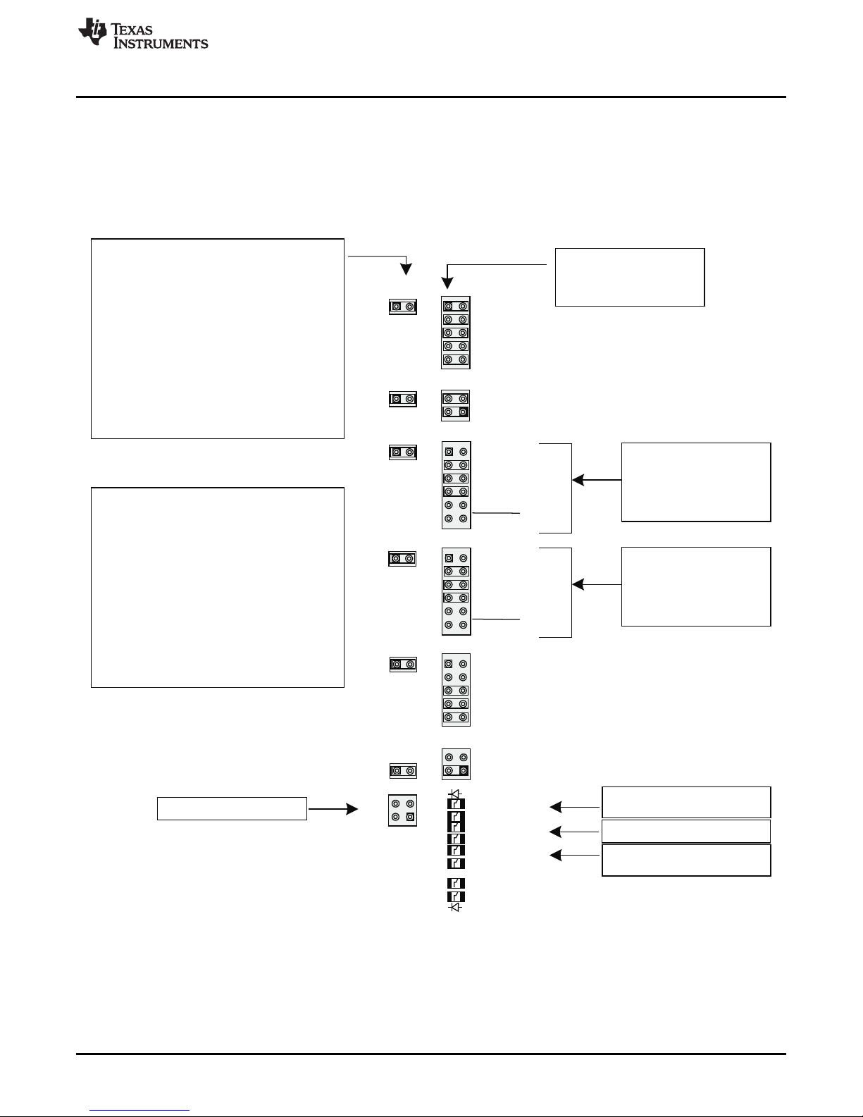
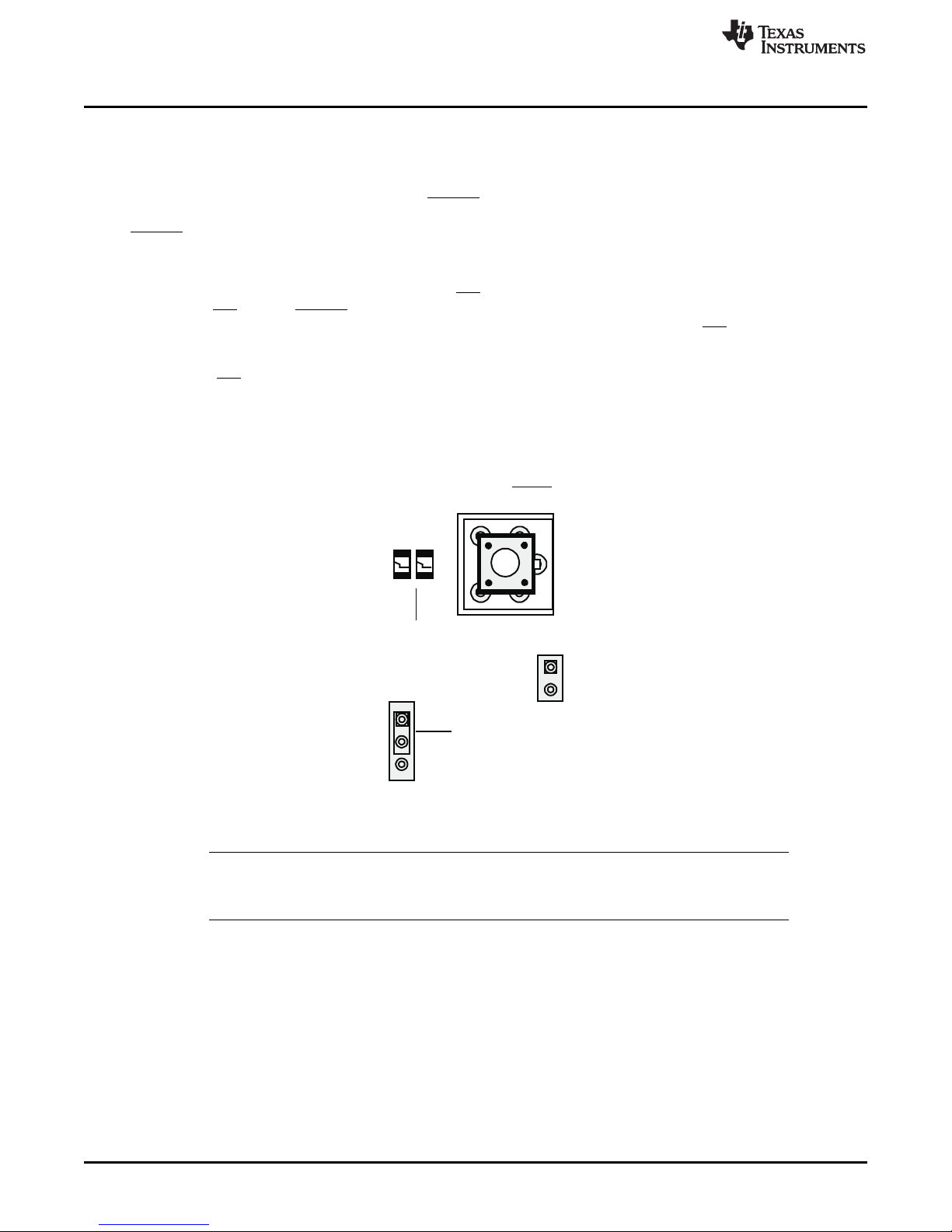
6 Control and Output Status Signals
All of the external control and status pins on the TLK6002EVM have been consolidated to a single location
on the board and broken out into several header blocks for easier reference. LEDs have been added to
the LOSA, LOSB, PRBS_PASSA, and PRBS_PASSB lines in addition to the headers for scope probes, to
allow easy monitoring of the High/Low value on the line. The LED is ON when the line is a Logic High, and
the LED is OFF when the line is a logic low. If the line is toggling, a dimming of the LED may be observed
as the LED is pulsing on and off relative to the activity on the line.
Control and Output Status Signals
Figure 8. Control Connectors (JMP17, JMP23, JMP26, JMP27, JMP29, JMP33, JMP43)
6.1 Control Signal and Status Pin Descriptions:
PRTAD[4:0]: Port Address. Used to select the Port ID.
SLLU132–October 2010 TLK6002 Dual-Channel, 0.47-Gbps to 6.25-Gbps, Multi-Rate Transceiver
Submit Documentation Feedback
Copyright © 2010, Texas Instruments Incorporated
Evaluation Module
11
Page 12

Control and Output Status Signals
PRTAD[4:1] selects the device port address. TLK6002 has two different PHY addresses (ports).
Selecting a unique PRTAD[4:1] per TLK6002 device allows 16 TLK6002 devices per MDIO bus.
Each channel can be accessed by setting the appropriate port address field within the serial
interface protocol transaction.
TLK6002 responds if the four MSBs of the inband PHY address field on MDIO protocol (PA[4:1])
matches PRTAD[4:1]. The LSB of PHY address field (PA[0]) determines which channel/port
within TLK6002 to respond to.
PRTAD[0] is not used functionally, but is present for device testability and compatibility with other
devices in the family of products.
Channel A responds to port address 0 within the block of two port addresses.
Channel B responds to port address 1 within the block of two port addresses.
PRTAD[0] must be grounded on the application board.
The PRTAD[3] pin in application mode must be biased with a pullup or pulldown resistor (or allow
for an isolation mechanism from the onboard driver) and not connected directly to a power or
ground plane. The application board allows the flexibility of easily reworking the PRTAD[3] signal
to a high level if the device debug is necessary (by including an uninstalled resistor to VDDO1).
REFCLK_A_SEL: Reference Clock Select Channel A. This input, when low, selects REFCLK_0_P/N as
the clock reference to Channel A SERDES macro. When high, REFCLK_1_P/N is selected as the clock
reference to Channel A SERDES macro. If software control is desired (register bit 0.1), this input signal
must be tied low. See Figure 4, “TLK6002 Reference Clock/Output Clock Architecture” of the TLK6002,
Dual-Channel 0.47Gbps to 6.25Gbps Multi-Rate Transceiver data sheet (SLLSE34) for more detail.
REFCLK_B_SEL: Reference Clock Select Channel B. This input, when low, selects REFCLK_0_P/N as
the clock reference to Channel B SERDES macro. When high, REFCLK_1_P/N is selected as the clock
reference to Channel B SERDES macro. If software control is desired (register bit 0.1), this input signal
must be tied low. See Figure 4, “TLK6002 Reference Clock/Output Clock Architecture” of the TLK6002
data sheet (SLLSE34) for more detail.
RATE_A[2:0]: Channel A Rate select pins. These pins put channel A into one of the four supported
(full/half/quarter/eighth) channel operation rates, enable software control, or enable Auto Rate Sense
(ARS):
www.ti.com
000 – Full Rate mode
001 – Half Rate mode
010 – Quarter Rate mode
011 – Eighth Rate mode
100 – Software Selectable Rate
101 – Channel A Auto Rate Sense (ARS) Function Enabled.
Channel A SERDES settings are determined by Channel A ARS machine. CLK_OUT_P/N selected
by CLK_OUT_SEL. See Table 9 of the TLK6002 data sheet (SLLSE34) for additional details on
CLK_OUT_P/N.
110 – Channel A Auto Rate Sense (ARS) Function Enabled.
Channel A SERDES settings are determined by Channel A ARS machine. CLK_OUT_P/N is
not selected by CLK_OUT_SEL. Channel B may not be simultaneously configured with
RATE_B = 110 with respect to CLK_OUT_P/N, this setting has the highest priority. See Table
9 of the TLK6002 data sheet (SLLSE34) for additional details on CLK_OUT_P/N.
111 – Channel A Auto Rate Sense (ARS) Function Enabled – Slave Mode.
If Channel B ARS is enabled (Rate B = 101 or 110 only):
Channel A SERDES settings are determined by Channel B ARS machine. CLK_OUT_P/N is
not selected by CLK_OUT_SEL. See Table 9 of the TLK6002 data sheet (SLLSE34) for
additional details on CLK_OUT_P/N.
12
TLK6002 Dual-Channel, 0.47-Gbps to 6.25-Gbps, Multi-Rate Transceiver SLLU132–October 2010
Evaluation Module
Copyright © 2010, Texas Instruments Incorporated
Submit Documentation Feedback
Page 13

www.ti.com
Control and Output Status Signals
If Channel B ARS is not enabled (Rate B = 000/001/010/011/111):
Channel A SERDES settings are determined by Channel A MDIO registers. CLK_OUT_P/N is
selected by CLK_OUT_SEL. See Table 9 of the TLK6002 data sheet (SLLSE34) for additional
details on CLK_OUT_P/N.
Channel A and B must not be in slave mode simultaneously. Both directions of Channel A are
controlled by these input signals.
The RATE_A[2] pin must be routed to an uninstalled header so that it can be driven externally in
the event that device debug is required. In application mode, it must be biased with a pullup or
pulldown resistor and not connected directly to a power or ground plane.
CODEA_EN: Encoder/Decoder Channel A Enable: When this pin is asserted high, the internal 8b/10b
encoder/decoder is enabled. This signal is ORed with MDIO register bits and must be pulled low through
a resistor if software control is desired. This pin must be routed to an uninstalled header so that it can be
driven externally in the even that device debug is required. In application mode, it must be biased with a
pullup or pulldown resistor and not connected directly to a power or ground plane.
LOSA: Channel A Receive Loss Of Signal (LOS) Indicator.
LOSA = 0, signal detected.
LOSA = 1, loss of signal.
Loss of signal detection is based on the input signal level. When RXAP/N has an input signal
of ≤75mVdfpp, LOSA is asserted (if enabled). The input signal must be greater than or equal
to 150mVdfpp for this function to operate reliably.
Other functions can be observed on LOSA real time, configured via MDIO.
During device reset (RESET_N asserted low), this pin is driven low. During pin-based power
down (PD_TRXA_N asserted low), this pin is floating. During register-based power down (1.15
asserted high), this pin is floating.
It is highly recommended that LOSA be brought to an easily accessible point on the
application board (header) in the event that debug is required.
PD_TRXA_N: Transceiver Power Down. When this pin is held low (asserted), Channel A is placed in
power-down mode. When de-asserted, Channel A operated normally. After de-assertion, a software data
path reset must be issued through the MDIO interface.
RATE_B[2:0]: Channel B Rate select pins. These pins put channel B into one of the four supported
(full/half/quarter/eighth) channel operation rates, enable software control, or enable Auto Rate Sense
(ARS):
000 – Full Rate mode
001 – Half Rate mode
010 – Quarter Rate mode
011 – Eighth Rate mode
100 – Software Selectable Rate
101 – Channel A Auto Rate Sense (ARS) Function Enabled.
Channel B SERDES settings are determined by Channel B ARS machine. CLK_OUT_P/N is
selected by CLK_OUT_SEL. See Table 9 of the TLK6002 data sheet (SLLSE34) for additional
details on CLK_OUT_P/N.
110 – Channel B Auto Rate Sense (ARS) Function Enabled.
Channel B SERDES settings are determined by Channel B ARS machine. CLK_OUT_P/N is
not selected by CLK_OUT_SEL. Channel A may not be simultaneously configured with
RATE_A = 110 with respect to CLK_OUT_P/N; this setting has the highest priority. See Table
9 of the TLK6002 data sheet (SLLSE34) for additional details on CLK_OUT_P/N.
111 – Channel B Auto Rate Sense (ARS) Function Enabled – Slave Mode
If Channel B ARS is enabled (Rate B = 101 or 110 only):
Channel B SERDES settings are determined by Channel B ARS machine. CLK_OUT_P/N is
not selected by CLK_OUT_SEL. See Table 9 of the TLK6002 data sheet (SLLSE34) for
additional details on CLK_OUT_P/N.
SLLU132–October 2010 TLK6002 Dual-Channel, 0.47-Gbps to 6.25-Gbps, Multi-Rate Transceiver
Submit Documentation Feedback
Evaluation Module
13
Copyright © 2010, Texas Instruments Incorporated
Page 14

Control and Output Status Signals
If Channel B ARS is not enabled (Rate B = 000/001/010/011/111):
Channel B SERDES settings are determined by Channel B MDIO registers. CLK_OUT_P/N is
selected by CLK_OUT_SEL. See Table 9 of the TLK6002 data sheet (SLLSE34) for additional
details on CLK_OUT_P/N.
Channel A and B must not be in slave mode simultaneously. Both directions of Channel A are
controlled by these input signals.
The RATE_B2 pin must be routed to an uninstalled header so that it can be driven externally
in the event that device debug is required. In application mode, it must be biased with a pullup
or pulldown resistor and not connected directly to a power or ground plane.
CODEB_EN: Encoder/Decoder Channel B Enable: When this pin is asserted high, the internal 8b/10b
encoder/decoder is enabled. This signal is ORed with MDIO register bits, and must be pulled low through
a resistor if software control is desired. This pin must be routed to an uninstalled header so that it can be
driven externally in the event that device debug is required. In application mode, it must be biased with a
pullup or pulldown resistor and not connected directly to a power or ground plane.
LOSB: Channel B Receive Loss Of Signal (LOS) Indicator.
LOSB = 0, signal detected.
LOSB = 1, loss of signal.
Loss of signal detection is based on the input signal level. When RXBP/N has an input signal
of ≤75 mVdfpp, LOSB is asserted (if enabled). The input signal must be greater than or equal
to 150mVdfpp for this function to operate reliably.
Other functions can be observed on LOSB real time, configured via MDIO.
During device reset (RESET_N asserted low), this pin is driven low. During pin-based power
down (PD_TRXB_N asserted low), this pin is floating. During register-based power down (1.15
asserted high), this pin is floating.
It is highly recommended that LOSB be brought to an easily accessible point on the
application board (header) in the event that debug is required.
www.ti.com
PD_TRXB_N: Transceiver Power Down. When this pin is held low (asserted), Channel B is placed in
power-down mode. When de-asserted, Channel B operated normally. After de-assertion, a software data
path reset must be issued through the MDIO interface.
AMUXB: SERDES Channel B Analog Testability I/O. This signal is used during the device manufacturing
process. It must be left unconnected in the device application.
AMUXA: SERDES Channel A Analog Testability I/O. This signal is used during the device manufacturing
process. It must be left unconnected in the device application.
TESTEN: Test Enable. This signal is used during the device manufacturing process. It must be grounded
through a resistor in the device application board. The application board must allow the flexibility of easily
reworking this signal to a high level if device debug is necessary (by including an uninstalled resistor to
VDDO2).
PRBS_EN: Enable PRBS: When this pin is asserted high, the internal PRBS generator and verifier
circuits are enabled on both transmit and receive data paths of both channels. This signal is logically
ORed with an MDIO register bit. PRBS 231-1 is selected by default, and can be changed in MDIO register
7.10:8. Note that PRBS is not possible in eighth rate mode.
The PRBS_EN pin must be routed to an uninstalled header so that it can be driven externally in the event
that device debug is required. In application mode, it must be biased with a pullup or pulldown resistor (or
allow for an isolation mechanism from the onboard driver) and not connected directly to a power or ground
plane.
CLK_OUT_SEL: Output Clock Selection. If ARS is not enabled and CLK_OUT_SEL is low, Channel A
recovered byte clock is output onto CLK_OUT_P/N. If ARS is not enabled and CLK_OUT_SEL is high,
Channel B recovered byte clock is output onto CLK_OUT_P/N. If software control is desired, (registered
bit 0.6), this input signal must be tied low. See Figure 4, “TLK6002 Reference Clock/Output Clock
Architecture” of the TLK6002 data sheet (SLLSE34) for more detail. If ARS is enabled, the function of
CLK_OUT_SEL is shown in Table 9 of the TLK6002 data sheet.
14
TLK6002 Dual-Channel, 0.47-Gbps to 6.25-Gbps, Multi-Rate Transceiver SLLU132–October 2010
Evaluation Module
Copyright © 2010, Texas Instruments Incorporated
Submit Documentation Feedback
Page 15

www.ti.com
GPI0: General Purpose Input Zero. This signal is used during the device manufacturing process. It must
be grounded through a resistor in the device application board. The application board must allow the
flexibility of easily reworking this signal to a high level if device debug is necessary (by including an
uninstalled resistor to VDDO2).
GPI1: General Purpose Input One. This signal can be used to logically combine an external status
condition with LOSA or LOSB if enabled in an MDIO register. Note that if GPI1 is low, LOSA/B is asserted
if a logical combination in enabled. Similarly, if GPI1 is high, LOSA/B is de-asserted. If unused, this input
must be grounded in the device application (not floating).
Control and Output Status Signals
SLLU132–October 2010 TLK6002 Dual-Channel, 0.47-Gbps to 6.25-Gbps, Multi-Rate Transceiver
Submit Documentation Feedback
Evaluation Module
15
Copyright © 2010, Texas Instruments Incorporated
Page 16

PRBS PASS Latch Circuits
7 PRBS PASS Latch Circuits
The TLK6002EVM has a Pass/Fail Latch circuit to aid in PRBS testing. The PRBS_PASSA and
PRBS_PASSB status signals have been routed out to Header JMP43 for monitoring with an oscilloscope.
Additionally, these signals are routed to the base of an NPN transistor that drives an LED on or off
depending on whether the PRBS_PASSA/B signals are High or Low. The blue LEDs D51 and D52 are a
good indication of general passing or general failing depending on whether the LED is on or off. However,
it is not a good method to easily monitor individual bit failures. An error counter can be read through the
MDIO register interface that contains the actual error count should the counter not have overflowed;
however, it requires the counter to be read in order to determine whether an error has occurred. With
proper setup and operation, the PRBS_PASS Latch circuits can quickly indicate whether an error has
occurred or not.
To properly operate the PRBS_PASS latches, configure the TLK6002 for PRBS operation either by pulling
the PRBS_EN line high or through the appropriate MDIO register settings. PRBS data is generated and
output on the Serial Transmit and the Serial Receive monitors for valid PRBS data and counts the number
of errors received. In addition to counting the errors, the PRBS_PASS line is high if the line is error free,
and transitions low for the duration of time that an error, or errors, are detected. Once the PRBS link is
established and running error free, pushing the PRBS_PASS RESET button resets the latch circuit, which
consists of a J/K flip-flop and a red and green LED to indicate the state of the flip-flop. When the J/K
flip-flop is reset, the green LED is lit until a high-to-low transition on the PRBS_PASS signal is observed.
Because the PRBS_PASS signal is connected to the clock input of the J/K flip-flop, a high-to-low transition
causes the flip-flop to toggle to the next state which turns OFF the green LED and turns ON the red LED.
The circuit remains in this state until the RESET button is pushed again, which resets the flip-flop to its
initial state.
www.ti.com
NOTE: If the PRBS_PASS lines are low, indicating constant PRBS failure and the PRBS_PASS
RESET buttons are pushed, the green LEDs lights and remain lit, which might be falsely
interpreted as a passing result. This is incorrect as the line was not ever passing and as long
as it is failing the PRBS_PASS line will be low and never have the high-to-low transition
required to toggle the state and light the red LED. This is not the intended operation of the
circuit, and this latch circuit must ONLY be used on a passing and correctly established
channel with valid PRBS data. An easy indication of whether the PRBS Latch may be used
is whether the blue PRBSA/B LEDs are on as well, because they can only be on if the
PRBS_PASS signals are high indicating a passing status. If the blue LEDs are not on, then
the green and red PRBS_PASS/Fail LEDs are not a valid indication of the status of the test.
16
TLK6002 Dual-Channel, 0.47-Gbps to 6.25-Gbps, Multi-Rate Transceiver SLLU132–October 2010
Evaluation Module
Copyright © 2010, Texas Instruments Incorporated
Submit Documentation Feedback
Page 17
RESISTOR
POWER
1P5/8V
GND
GND
GND
AMUXB
AMUXA
TESTEN
CLKOUTSEL
PRBSEN
PRBSBFAIL
PRBSBPASS
PRBSB
PRBSA
PRBSA FAIL
PRBSA PASS
A
B
LOSA
LOSB
PRBSPASS
PRBSA
PRBSB
LATCH LATCH
RESET
RESET
SW4
SW3
D41
D42
D4
D3
D52
D51
D50
D49
JMP43
JMP23
JMP17
JMP16
JMP27
PRBS_PASSBSIGNAL
LATCHLEDSRESET BY
PRESSINGSW4
PRBS_PASSA SIGNAL
LATCHLEDSRESET BY
PRESSINGSW3
BLUEPRBS_PASSSIGNAL LEDS
PRBS_PASSSIGNALSCANBE
OBSERVEDWITH A SCOPEHERE
ENABLE THEPRBSGENERATOR/
ANALYZERFUNCTIONBY
REMOVING THISSHUNT AND
PULLING THELINEHIGH
www.ti.com
PRBS PASS Latch Circuits
Figure 9. TLK6002 EVM MDIO Connector (JMP30)
SLLU132–October 2010 TLK6002 Dual-Channel, 0.47-Gbps to 6.25-Gbps, Multi-Rate Transceiver
Submit Documentation Feedback
Copyright © 2010, Texas Instruments Incorporated
Evaluation Module
17
Page 18
GND
GND
MDC
MDIO
MDIO
JMP30
ALL NON-LABELEDPINS
ARENO-CONNECTS
MDIO
8 MDIO
The TLK6002 supports the Management Data Input/Output (MDIO) Interface as defined in Clause 22 of
the IEEE 802.3 Ethernet Specification. The MDIO allows register-based management and control of the
serial links. Normal operation of the TLK6002 is possible without the use of this interface; however, some
additional features are accessible only through the MDIO interface.
The MDIO Management Interface consists of a bidirectional data path (MDIO) and a clock reference
(MDC). The port address is determined by control pins PRTAD[4:0
In Clause 22, the top four control pins PRTAD[4:1] determine the device port address. In this mode, the
two individual channels in TLK6002 are classified as two different ports. Therefore, any PRTAD[4:1] value
has two ports per TLK6002. The TLK6002 responds if the four MSBs of PHY address field on MDIO
protocol (PA[4:1]) matches PRTAD[4:1]. The LSB of PHY address field (PA[0]) determines which
channel/port within the TLK6002 to respond to.
If PA[0] = 1’b0, TLK6002’s Channel A responds.
If PA[0] = 1’b1, TLK6002’s Channel B responds.
Write transactions which address an invalid register or read-only registers are ignored. Read transactions
of invalid registers return a 0.
The bidirectional MDIO pin must be externally pulled up to 1.5 V or 1.8 V (VDDO) with an appropriate
resistor value as per the IEEE802.3 Clause 22/45 MDIO Standard.
The supplied MDIO EVM uses an FPGA with 2.5-V I/O signal levels whereas the TLK6002 requires either
1.5-V or 1.8-V I/O levels on these signals. Therefore, bidirectional level shifters have been provided on
board that level shift the 2.5-V MDIO and MDC signals to the appropriate 1p5/8V levels. If a different
MDIO controller id used that already has 1.5-V or 1.8-V signal levels, resistors R530, R531, R532, and
R533 can be removed; thus, disconnecting the level shifters and resistors R469 and R470 can be installed
which connects the TLK6002 MDIO and MDC signal pins directly to the pins of JMP30. A third option of
using NFETs as level shifters has also been provided, if this option is desired in the end application.
Removing resistors R530, R531, R532, and R533, as well R469 and R470 if they were installed, and
installing an appropriate NFET such as Fairchild’s FDV301N allows for this third option of level shifting to
be evaluated.
www.ti.com
Figure 10. TLK6002 EVM MDIO Connector (JMP30)
18
TLK6002 Dual-Channel, 0.47-Gbps to 6.25-Gbps, Multi-Rate Transceiver SLLU132–October 2010
Evaluation Module
Copyright © 2010, Texas Instruments Incorporated
Submit Documentation Feedback
Page 19
GND
GND
GND
GND
GND
TDI
TDO
TRST
TMS
TCK
JTAG
JMP35
www.ti.com
9 JTAG
The EVM also provides a separate connector to support the full five-pin JTAG interface of the TLK6002
with onboard level shifters to be compatible with most standard JTAG Control Interfaces to be used for
manufacturing tests. Pullup resistors on the 3.3-V (header) side of the level shifter are not installed by TI
but can be installed if an open-drain type of controller is used which requires the use of external pullup
resistors.
JTAG
TDI: JTAG Input Data. TDI is used to serially shift test data and test instructions into the device
during the operation of the test port. In system applications where JTAG is not implemented, this
input signal can be left floating. During pin-based power down (PD_TRXA_N and PD_TRXB_N
asserted low), this pin is not pulled up. During register-based power down (1.15 asserted high for
both channels), this pin is pulled up normally.
TDO: JTAG Output Data. TDO is used to serially shift test data and test instructions out of the
device during operation of the test port. When the JTAG port is not in use, TDO is in a
high-impedance state. During device reset (RESET_N asserted low), this pin is floating. During
pin-based power down (PD_TRXA_N and PD_TRXB_N asserted low), this pin is floating. During
register-based power down (1.15 asserted high on both channels), this pin is floating.
TMS: JTAG Mode Select. TMS is used to control the state of the internal test-port controller. In
system applications where JTAG is not implemented, this input signal can be left unconnected.
During pin-based power down (PD_TRXA_N and PD_TRXB_N asserted low), this pin is not
pulled up. During register-based power down (1.15 asserted high both channels), this pin is
pulled up normally.
TCK: JTAG Clock. TCK is used to clock state information and test data into and out of the device
during boundary scan operation. In system applications where JTAG is not implemented, this
input signal must be grounded.
TRST_N: JTAG Test Reset. TRST_N is used to reset the JTAG logic into system operational
mode. This input can be left unconnected in the application and is pulled down internally,
disabling the JTAG circuitry. If JTAG is implemented on the application board, this signal must be
de-asserted (high) during JTAG system testing, and otherwise asserted (low) during normal
operation mode. During pin-based power down (PD_TRXA_N and PD_TRXB_N asserted low),
this pin is not pulled down. During register-based power down (1.15 asserted high on both
channels), this pin is pulled down normally.
NOTE: TRST_N must be tied low when the JTAG port is not in use and during normal operation of
the port as shown in Figure 11 because an external pullup resistor is provided. If you have
no need to use the JTAG port, removing resistor R423 allows the internal pulldown to disable
the circuitry and installing resistor R426 provides an external pulldown on this pin.
Figure 11. TLK6002 EVM JTAG Connector (JMP35)
SLLU132–October 2010 TLK6002 Dual-Channel, 0.47-Gbps to 6.25-Gbps, Multi-Rate Transceiver
Submit Documentation Feedback
Evaluation Module
19
Copyright © 2010, Texas Instruments Incorporated
Page 20
MAINRST
RST
RST
MAIN
MANUAL RESET
GND
MAIN
RST BUTTON
RST
GND
JMP15
SW1
D1
D2
JMP14
Reset
10 Reset
The TLK6002EVM comes configured for Manual Reset operations involving the Pushbutton Reset Switch
(SW1). When switch SW1 is pressed, the TLK6002 device RESET pin (RST_N) goes LOW and the entire
TLK6002 device is reinitialized. A TI TPS3125J18 Ultra Low Voltage Processor Supervisory Circuit is used
to control the Reset line. During power on, RESET pin of U2 is asserted when the supply voltage
becomes higher than 0.75 V. Thereafter, the supply voltage supervisor monitors the voltage and keeps
RESET output active as long as the voltage remains below the threshold voltage (VIT). An internal timer
delays the return of the output to the inactive state (high) to ensure proper system reset. The delay time, t
= 180 ms, starts after the voltage has risen above the threshold voltage (VIT).
A manual reset input to the supervisory circuit, MR, accepts the input from the pushbutton switch SW1. A
low level at MR causes RESET to become active, thus resetting the TLK6002 device whenever the
pushbutton RESET is pressed. By placing a jumper on JMP15, the Manual Reset (MR) is tied hard to
ground causing the TLK6002 to be held in a constant state of Reset without the need to continually hold
the Reset Pushbutton SW1. The Supervisory circuit released the Reset line to a HIGH 180 ms (td) from
the time the MR line becomes greater than the threshold voltage (VIT).
By removing the jumper from JMP14, the Supervised Reset Circuit is disconnected from the RST_N line.
Reset control from an external controller or piece of equipment can be connected directly to pin 2
(RST_N) of JMP14 and a ground pin GND has been added to the JMP14 header next to the RST_N pin
to allow easy access for the return current on that cable.
www.ti.com
d
Figure 12. RESET Switch – SW1, JMP14, or JMP15
NOTE: The Jumper on JMP14 connecting RESET SW to RST_N must be connected as shown in
order to cause the TLK6002 to be reset and reinitialized If switch SW1 is pressed, the device
RESET pin (RST_N) goes LOW, the entire TLK6002 device is reinitialized.
20
TLK6002 Dual-Channel, 0.47-Gbps to 6.25-Gbps, Multi-Rate Transceiver SLLU132–October 2010
Evaluation Module
Copyright © 2010, Texas Instruments Incorporated
Submit Documentation Feedback
Page 21
19
18
17
16
15
14
13
12
11
10
9
8
7
6
5
4
3
2
1
0
19
18
17
16
15
14
13
12
11
10
9
8
7
6
5
4
3
2
1
0
1P5/8V
TDA0..19
TDA0..19
RDA0..19
GND
GND
JMP145
JMP38
JMP37
GND
GND
TXCLKA
RXCLKA
PARALLEL SIGNAL
BIT NUMBER
PARALLEL SIGNAL
BIT NUMBER
PIN TYPEOFROW
PINNAMES
www.ti.com
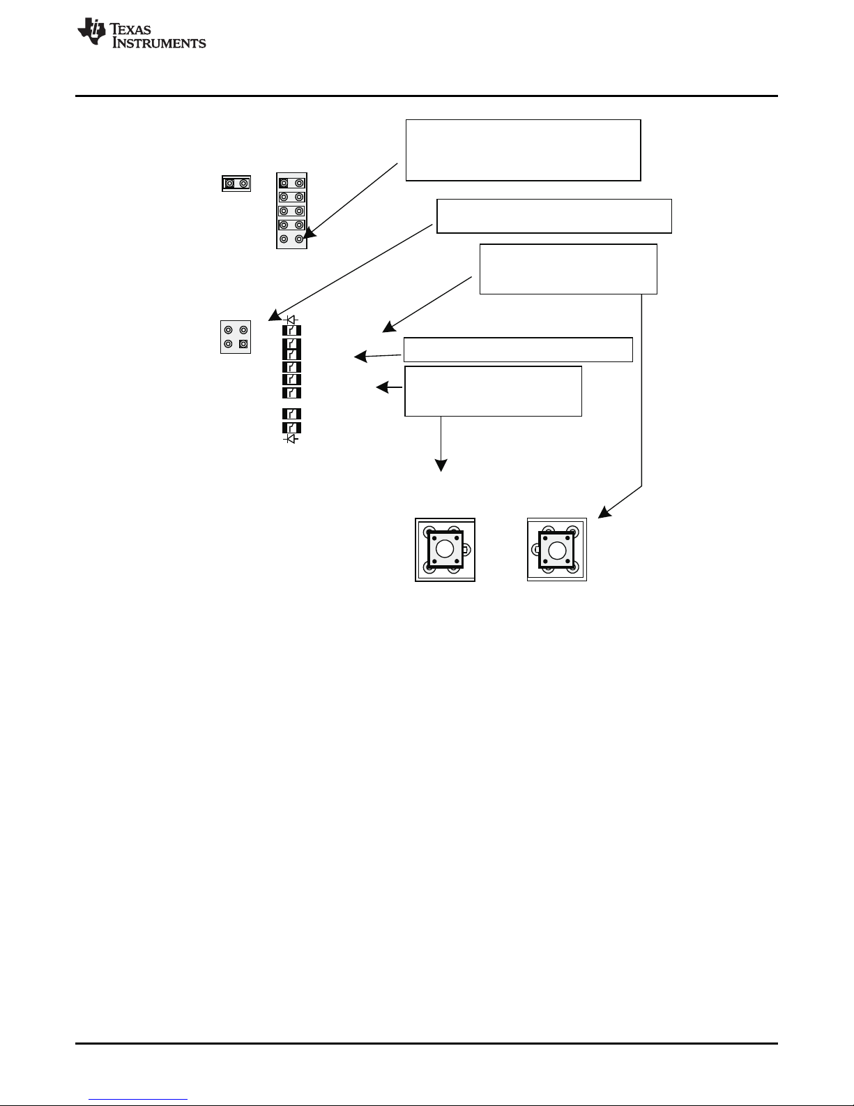
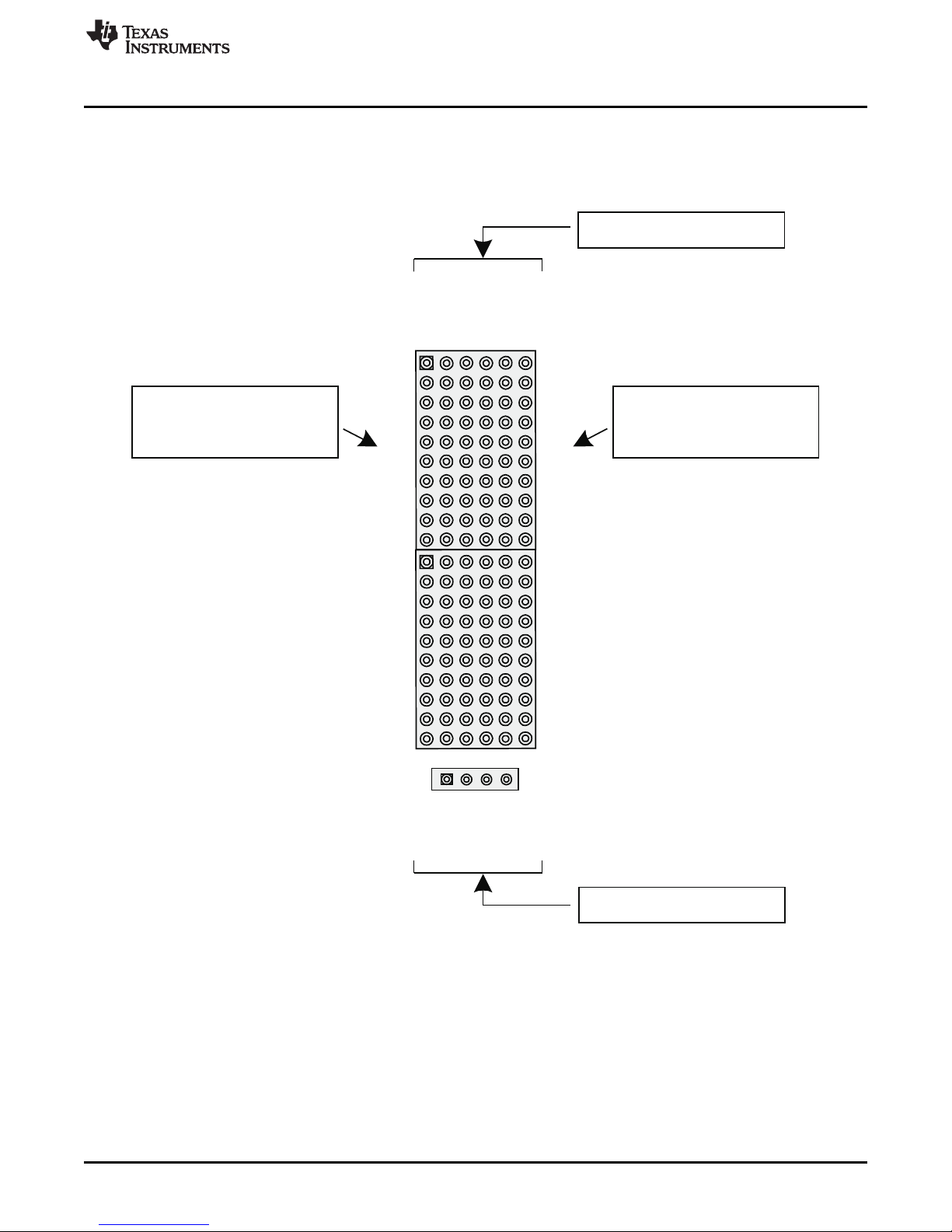
11 Parallel Signals
The parallel signals on the TLK6002EVM have been routed to a 0.1-in. header block that is configured like
Figure 13. All RD pins on header blocks RDA/B[7:0], RDA/B[15:8], as well as all TDA/B pins on header
blocks TDA/B[7:0], TDA/B[15:8], have matched trace lengths to themselves ±0.5 mil.
Parallel Signals
Parallel Loopback, shown in Figure 14, can be easily implemented by placing jumpers on the RDx/TDx
pins of the header. For example, placing a jumper on pins 4 and 5 of JMP37 loops back TDA19 to
RDA19.
The Transmit Data Clocks and Receive Data Clocks are located in header blocks JMP145 and JMP146
with the clock pins next to each other. These signals are the parallel side input and output clocks per
channel. During Parallel Loopback, the clocks can be shorted together as shown in Figure 14.
Figure 13. Parallel Signal Header Block Diagram
SLLU132–October 2010 TLK6002 Dual-Channel, 0.47-Gbps to 6.25-Gbps, Multi-Rate Transceiver
Submit Documentation Feedback
Copyright © 2010, Texas Instruments Incorporated
Evaluation Module
21
Page 22
19
18
17
16
15
14
13
12
11
10
9
8
7
6
5
4
3
2
1
0
19
18
17
16
15
14
13
12
11
10
9
8
7
6
5
4
3
2
1
0
1P5/8V
TDA0..19
TDA0..19
RDA0..19
GND
GND
JMP145
JMP38
JMP37
GND
GND
TXCLKA
RXCLKA
PARALLEL
LOOPBACK
Parallel Signals
www.ti.com
Additional GND and VDD pins have been added into the header block for several reasons. The GND pins
next to the RDA/B and TDA/B pins provide a convenient ground reference for a scope probe or coaxial
cables. The additional TDA/B row and VDD pins allow a static pattern to be driven into the TDA/B bus by
placing jumpers across either the TDA and 1p5/8V pins for a HIGH, or TDA/B and GND pins for a LOW
eliminating the need for cables during quick tests. The extra row of TDA/B can also be used to monitor the
signals on the TDA/B pins. Figure 15 shows a clock pattern (01010101010101010101) on TDA[19:0].
Figure 14. Parallel Loopback Example
22
TLK6002 Dual-Channel, 0.47-Gbps to 6.25-Gbps, Multi-Rate Transceiver SLLU132–October 2010
Evaluation Module
Copyright © 2010, Texas Instruments Incorporated
Submit Documentation Feedback
Page 23

19
18
17
16
15
14
13
12
11
10
9
8
7
6
5
4
3
2
1
0
19
18
17
16
15
14
13
12
11
10
9
8
7
6
5
4
3
2
1
0
GND
GND
JMP145
JMP38
JMP37
GND
GND
TXCLKA
RXCLKA
STATICCLOCK
DRIVENON TDA[19:0]
www.ti.com
Peripheral Ports
Figure 15. TDA[19:0] Static Clock Data Pattern Example
12 Peripheral Ports
The TLK6002EVM can support three small peripheral boards which can contain any sort of additional
circuitry required for effective evaluation of the TLK6002 device. Examples of additional circuitry that can
be implemented include a clock source such as an oscillator with multiplier/divider chip, FPGA, CPLD, or
even an optical module to name a few. All of the power rails (1.2 V, 1.5/8 V, 2.5 V, 3.3 V and 5 V) have
been provided to allow for minimal power circuitry on the peripheral board itself as well as the global reset
signal which is connected to the TLK6002 Reset pin. TI is developing an optical module peripheral board
and a clock multiplier and divider peripheral board specifically for use with the TLK6002EVM which will be
capable of providing practically any clock frequency needed for operation of the TLK6002 device.
However, these boards are not complete and ready for distribution with the TLK6002EVM. See sheet 28
of the TLK6002EVM schematic located in Section 14 as well as the line item in the bill of materials for
connector part number information.
SLLU132–October 2010 TLK6002 Dual-Channel, 0.47-Gbps to 6.25-Gbps, Multi-Rate Transceiver
Submit Documentation Feedback
Evaluation Module
23
Copyright © 2010, Texas Instruments Incorporated
Page 24

TLK6002
GND GND
GND GND GND GND GND GND
VADJ5V
1P2V
3P3V2P5V1P5V1P8V
1P0V
BANANAJACK BANANA JACKBANANAJACK BANANAJACK BANANAJACK
BJACK
BJACK
P2
P3
P16
P4
P5
P6 P7 P8 P9
P1
P20 P15 P29
P33
P30
P23
5V
PLUG
1P2V
1P2VREG
1P2V
REG
+5V
REG
REG
REG
REGREG
REG
REGREGREG
1P0V
1P0VREG
1P8V
1P5/8V
1P5V
1P8V
1P8VREG 1P5VREG
1P5V 2P5V
3P3V
2P5VREG
3P3VREG
1P0V
REG REG
1P8V 1P5V
2P5V
3P3V
REGEN
MIN
REGEN
REGEN
REGEN
REGEN
REGEN
GND
GND
GND
GND
GNDGND
NOM
MAX
AUTO
(VADJ)
ADJ
MIN
ADJ
NOM AUTO
(VADJ)
MAXMAX
NOM
MIN
ADJ
AUTO
(VADJ)
AUTO
(VADJ)
AUTO
(VADJ)
AUTO
(VADJ)
MAX
NOM
MIN
ADJ
MAX
NOM
MIN
ADJ
MAX
NOM
MIN
ADJ
MAX
(3V)
MIN
(1V)
NOM
(2V)
VADJBJ
ON
VADJ
OFF
(3.8V)
GLOBAL
VOLTAGE
ADJUST
RESISTOR
POWER
RESISTOR
POWER
RESISTOR
POWER
RESISTOR
POWER
RESISTOR
POWER
1P5/8V
1P5/8V
1P5/8V
1P5/8V
1P5/8V
1P5/8V
PRTAD0
PRTAD1
PRTAD2
PRTAD3
PRTAD4
REFCLKA SEL
REFCLKBSEL
RATEA 2
RATEA 1
RATEA 0
CODEAEN
LOSA
PD TRXA
GND
GND
GND
GND
GND
GND
GND
GND
GND
GND
RATEB2
RATEB1
RATEB0
CODEBEN
LOSB
PD TRXB
AMUXB
AMUXA
TESTEN
CLKOUTSEL
PRBSEN
GPI1
GPI0
PRBSBFAIL
PRBSBPASS
PRBSB
PRBSA
PRBSAFAIL
PRBSAPASS
A
B
LOSA
LOSB
MDC
MDIO
5V
1P5/8V
PRBSPASS
GND
GND
TXCLKA
RXCLKA
GND
GND
TXCLKB
RXCLKB
SCFG1
SOUT
SIN
SCFG0
SCLK
GND
GND
GND
GND
GND
GND
GND
GND
GND
GND
GND
GND
GND
GND
SCL
SDO
SDI
CS
TDI
TDO
TRST
TMS
TCK
GND
GND
GND
G
N
D
G
N
D
GND
1P0V
1P5/8V
DVDD
VD
D
R
A
VRE
F
T
VDDRB
PLN
LED
MNT
0P75V
0P9V
PLN
LED
MNT
PLN
LED
MNT
PLN
LED
MNT
PLN
LED
MNT
PLN
LED
MNT
PLN
LED
MNT
PLN
LED
MNT
PLN
LED
MNT
PLN
LED
MNT
PLN
LED
MNT
PLN
LED
MNT
PLN
LED
MNT
PLN
LED
MNT
PLN
LED
MNT
PWR
EN
GND
PWR
EN
GND
PWR
EN
GND
PWR
EN
GND
PWR
EN
GND
PWR
EN
GND
PWR
EN
GND
PWR
EN
GND
PWR
EN
GND
PWR
EN
GND
PWR
EN
GND
VREFT
VDDRB
VDDRA
1P5/8V
3P3V2P5V
1P8V
1P5V1P0V1P2VDVDD
1P8V
1P5V
1P8V1P5V
1P5V
1P8V
LEDMONITOR LEDMONITOR
LEDMONITOR
LEDMONITOR
LEDMONITOR
LEDMONITOR
LEDMONITOR
LEDMONITOR
REGULATOR
ADJUST
OFF
MAX
NOM
MIN
MAINRST
RST
RST
MAIN
MANUAL RESET
GND
MAIN
RST BUTTON
RST
GND
5V
3P3V
2P5V
1P8V
1P5V
1P2V
1P0V
DVDD
1P5V
1P8V
1P5V
1P8V
1P5V 1P8V
0P75V
0P9V
VREFT
VDDRB
VDDRA
1P5/8V
19
18
17
16
15
14
13
12
11
10
9
8
7
6
5
4
3
2
1
0
19
18
17
16
15
14
13
12
11
10
9
8
7
6
5
4
3
2
1
0
19
18
17
16
15
14
13
12
11
10
9
8
7
6
5
4
3
2
1
0
19
18
17
16
15
14
13
12
11
10
9
8
7
6
5
4
3
2
1
0
TLK6002
EVM
6519192
REVNA
1P5/8V
TDA0..19
TDA0..19
RDA0..19
GND
GND
1P5/8V
TDB0..19
TDB0..19
RDB0..19
GND
GND
MDIO
PRBSA
PRBSB
LATCH LATCH
RESET
RESET
STCI JTAG
SPI
JMP63
JMP59 JMP70 JMP58 JMP85 JMP149
JMP81
C187
C188
C189
P2
JMP89
U69
U12
JMP53
R106
C109
C108
R105
C107
JMP52
JMP56
R149
R150
R159
R152
R155
R162
U20
R158
R161
R139
R141
R142
R140
U16
R144
R143
R148
R145
R151
R153
JMP105
JMP104
JMP103
JMP102
U31
D5
D6
D7
D8
D16
D15
D14
D13
D12
D10
D11
D20
D22
D32
D34
D38
D37
D33
D31
D21
JMP15
SW1
D1
D2
JMP14
JMP39
JMP40
JMP146
JMP45
JMP35
JMP36
SW4
SW3
JMP145
JMP38
JMP37
V18V1
A18
A1A1
U1
JMP30
D41
D42
D4
D3
D52
D51
D50
D49
JMP43
JMP23
JMP21
JMP17
JMP16
JMP27
JMP25
JMP26
JMP24
JMP29
JMP28
JMP33
JMP31
C136
C139
C138
C135
C116
C115
C169
C170
C171
JMP57
C137
JMP55
U14
U13
R123
R122
C114
R124
JMP54
JMP51
R89
R88
C102
C101
C100
JMP50
R90
U10
JMP49
R72
R71
C93
C95
C94
JMP48
R73
U8
JMP47
R55
R54
C86
C87
C88
JMP46
R56
U6
U67
JMP148
R363
R362
C234
C236
C235
R364
JMP147
U70
U7
U9
U11
JMP138
U64
C168
JMP139
JMP140
C167
C141
C142
C145
C144
C143
JMP132
JMP134
U58
JMP133
C125
C126
C127
JMP129
U55
JMP130
JMP131
JMP114
C131
C132
C133
C158
C159
C160
JMP115
JMP116
U40
U37
JMP113
JMP112
JMP95
JMP94
U25
JMP96
JMP97
JMP98
JMP99
U28
JMP100
JMP101
R107
JMP7
J
MP4
JMP8
JMP6
JMP1
JMP3
T
X
A
N
T
X
A
P
R
X
A
N
R
X
A
P
RXBP
R
X
B
N
T
X
B
P
T
X
B
N
C
L
K
1
N
R
E
F
C
L
K
1
P
R
E
F
C
L
K
0
N
R
E
F
C
L
K
0
P
R
E
F
O
U
T
N
C
L
O
C
K
O
U
T
P
C
L
O
C
K
J
1
0
J9
J
1
1
J
1
2
J
1
4
J
1
3
J
7
J
5
J
8
J6
J
2
J
4
J
1
J
3
CLOCK
OUT
PULSE
GENERATOR
`
POWER
SUPPLY
5V
PARALLEL
BERT
TXD
GENERATOR
RXD
ANALYZER
TexasInstruments
MDIOEvaluationBoard
4
U1
0
MDIO
Addres
s
GND
Vin
U9
U1
2
Vin
U2
U3
J2
U7
J1
P1
U6
ALTER
A
MAX
OSC
COMBO
POWER
SUPPLY
7V
Test and Setup Configurations
13 Test and Setup Configurations
The device reset requirements and setup procedure to configure the TLK3132 can be found in the latest
version of the TLK6002 data sheet (SLLSE34). Always refer to the latest release of the data sheet for the
latest reset, setup, and initialization procedures.
The following figures show some generic test setups using the TLK6002EVM.
www.ti.com
Figure 16. Example TLK6002EVM Test Configuration – Serial Loopback
24
TLK6002 Dual-Channel, 0.47-Gbps to 6.25-Gbps, Multi-Rate Transceiver SLLU132–October 2010
Evaluation Module
Copyright © 2010, Texas Instruments Incorporated
Submit Documentation Feedback
Page 25

TLK6002
GND GND
GND GND GND GND GND GND
VADJ5V
1P2V
3P3V2P5V1P5V1P8V
1P0V
BANANAJACK BANANA JACKBANANAJACK BANANAJACK BANANAJACK
BJACK
BJACK
P2
P3
P16
P4
P5
P6 P7 P8 P9
P1
P20 P15 P29
P33
P30
P23
5V
PLUG
1P2V
1P2VREG
1P2V
REG
+5V
REG
REG
REG
REGREG
REG
REGREGREG
1P0V
1P0VREG
1P8V
1P5/8V
1P5V
1P8V
1P8VREG 1P5VREG
1P5V 2P5V
3P3V
2P5VREG
3P3VREG
1P0V
REG REG
1P8V 1P5V
2P5V
3P3V
REGEN
MIN
REGEN
REGEN
REGEN
REGEN
REGEN
GND
GND
GND
GND
GNDGND
NOM
MAX
AUTO
(VADJ)
ADJ
MIN
ADJ
NOM AUTO
(VADJ)
MAXMAX
NOM
MIN
ADJ
AUTO
(VADJ)
AUTO
(VADJ)
AUTO
(VADJ)
AUTO
(VADJ)
MAX
NOM
MIN
ADJ
MAX
NOM
MIN
ADJ
MAX
NOM
MIN
ADJ
MAX
(3V)
MIN
(1V)
NOM
(2V)
VADJBJ
ON
VADJ
OFF
(3.8V)
GLOBAL
VOLTAGE
ADJUST
RESISTOR
POWER
RESISTOR
POWER
RESISTOR
POWER
RESISTOR
POWER
RESISTOR
POWER
1P5/8V
1P5/8V
1P5/8V
1P5/8V
1P5/8V
1P5/8V
PRTAD0
PRTAD1
PRTAD2
PRTAD3
PRTAD4
REFCLKA SEL
REFCLKBSEL
RATEA 2
RATEA 1
RATEA 0
CODEAEN
LOSA
PD TRXA
GND
GND
GND
GND
GND
GND
GND
GND
GND
GND
RATEB2
RATEB1
RATEB0
CODEBEN
LOSB
PD TRXB
AMUXB
AMUXA
TESTEN
CLKOUTSEL
PRBSEN
GPI1
GPI0
PRBSBFAIL
PRBSBPASS
PRBSB
PRBSA
PRBSAFAIL
PRBSAPASS
A
B
LOSA
LOSB
MDC
MDIO
5V
1P5/8V
PRBSPASS
GND
GND
TXCLKA
RXCLKA
GND
GND
TXCLKB
RXCLKB
SCFG1
SOUT
SIN
SCFG0
SCLK
GND
GND
GND
GND
GND
GND
GND
GND
GND
GND
GND
GND
GND
GND
SCL
SDO
SDI
CS
TDI
TDO
TRST
TMS
TCK
GND
GND
GND
G
N
D
G
N
D
GND
1P0V
1P5/8V
DVDD
VD
D
R
A
VRE
F
T
VDDRB
PLN
LED
MNT
0P75V
0P9V
PLN
LED
MNT
PLN
LED
MNT
PLN
LED
MNT
PLN
LED
MNT
PLN
LED
MNT
PLN
LED
MNT
PLN
LED
MNT
PLN
LED
MNT
PLN
LED
MNT
PLN
LED
MNT
PLN
LED
MNT
PLN
LED
MNT
PLN
LED
MNT
PLN
LED
MNT
PWR
EN
GND
PWR
EN
GND
PWR
EN
GND
PWR
EN
GND
PWR
EN
GND
PWR
EN
GND
PWR
EN
GND
PWR
EN
GND
PWR
EN
GND
PWR
EN
GND
PWR
EN
GND
VREFT
VDDRB
VDDRA
1P5/8V
3P3V2P5V
1P8V
1P5V1P0V1P2VDVDD
1P8V
1P5V
1P8V1P5V
1P5V
1P8V
LEDMONITOR LEDMONITOR
LEDMONITOR
LEDMONITOR
LEDMONITOR
LEDMONITOR
LEDMONITOR
LEDMONITOR
REGULATOR
ADJUST
OFF
MAX
NOM
MIN
MAINRST
RST
RST
MAIN
MANUAL RESET
GND
MAIN
RST BUTTON
RST
GND
5V
3P3V
2P5V
1P8V
1P5V
1P2V
1P0V
DVDD
1P5V
1P8V
1P5V
1P8V
1P5V 1P8V
0P75V
0P9V
VREFT
VDDRB
VDDRA
1P5/8V
19
18
17
16
15
14
13
12
11
10
9
8
7
6
5
4
3
2
1
0
19
18
17
16
15
14
13
12
11
10
9
8
7
6
5
4
3
2
1
0
19
18
17
16
15
14
13
12
11
10
9
8
7
6
5
4
3
2
1
0
19
18
17
16
15
14
13
12
11
10
9
8
7
6
5
4
3
2
1
0
TLK6002
EVM
6519192
REVNA
1P5/8V
TDA0..19
TDA0..19
RDA0..19
GND
GND
1P5/8V
TDB0..19
TDB0..19
RDB0..19
GND
GND
MDIO
PRBSA
PRBSB
LATCH LATCH
RESET
RESET
STCI JTAG
SPI
JMP63
JMP59 JMP70 JMP58 JMP85 JMP149
JMP81
C187
C188
C189
P2
JMP89
U69
U12
JMP53
R106
C109
C108
R105
C107
JMP52
JMP56
R149
R150
R159
R152
R155
R162
U20
R158
R161
R139
R141
R142
R140
U16
R144
R143
R148
R145
R151
R153
JMP105
JMP104
JMP103
JMP102
U31
D5
D6
D7
D8
D16
D15
D14
D13
D12
D10
D11
D20
D22
D32
D34
D38
D37
D33
D31
D21
JMP15
SW1
D1
D2
JMP14
JMP39
JMP40
JMP146
JMP45
JMP35
JMP36
SW4
SW3
JMP145
JMP38
JMP37
V18V1
A18
A1A1
U1
JMP30
D41
D42
D4
D3
D52
D51
D50
D49
JMP43
JMP23
JMP21
JMP17
JMP16
JMP27
JMP25
JMP26
JMP24
JMP29
JMP28
JMP33
JMP31
C136
C139
C138
C135
C116
C115
C169
C170
C171
JMP57
C137
JMP55
U14
U13
R123
R122
C114
R124
JMP54
JMP51
R89
R88
C102
C101
C100
JMP50
R90
U10
JMP49
R72
R71
C93
C95
C94
JMP48
R73
U8
JMP47
R55
R54
C86
C87
C88
JMP46
R56
U6
U67
JMP148
R363
R362
C234
C236
C235
R364
JMP147
U70
U7
U9
U11
JMP138
U64
C168
JMP139
JMP140
C167
C141
C142
C145
C144
C143
JMP132
JMP134
U58
JMP133
C125
C126
C127
JMP129
U55
JMP130
JMP131
JMP114
C131
C132
C133
C158
C159
C160
JMP115
JMP116
U40
U37
JMP113
JMP112
JMP95
JMP94
U25
JMP96
JMP97
JMP98
JMP99
U28
JMP100
JMP101
R107
JMP7
J
MP4
JMP8
JMP6
JMP1
JMP3
T
X
A
N
T
X
A
P
R
X
A
N
R
X
A
P
RXBP
R
X
B
N
T
X
B
P
T
X
B
N
C
L
K
1
N
R
E
F
C
L
K
1
P
R
E
F
C
L
K
0
N
R
E
F
C
L
K
0
P
R
E
F
O
U
T
N
C
L
O
C
K
O
U
T
P
C
L
O
C
K
J
1
0
J9
J
1
1
J
1
2
J
1
4
J
1
3
J
7
J
5
J
8
J6
J
2
J
4
J
1
J
3
CLOCK
OUT
PULSE
GENERATOR
`
POWER
SUPPLY
5V
TexasInstruments
MDIOEvaluationBoard
4
U1
0
MDIO
Addres
s
GND
Vin
U9
U1
2
Vin
U2
U3
J2
U7
J1
P1
U6
ALTER
A
MAX
OSC
COMBO
POWER
SUPPLY
7V
SERIAL BERT
RD+/-
GENERATOR
TD+/-
ANALYZER
www.ti.com
Test and Setup Configurations
Figure 17. Example TLK6002 EVM Test Configuration – Parallel Loopback
SLLU132–October 2010 TLK6002 Dual-Channel, 0.47-Gbps to 6.25-Gbps, Multi-Rate Transceiver
Submit Documentation Feedback
Copyright © 2010, Texas Instruments Incorporated
25
Evaluation Module
Page 26
5
5
4
4
3
3
2
2
1
1
D D
C C
B B
A A
------- xx/xx/xx
REVISIONS
ECR
ECR NUMBER DATE
6519192
TLK6002 EVM
J. NERGER
S. GREGORY
J. NERGER
09/29/09
09/29/09
09/29/09
COVER PAGE
B - 28
Size Document Number Rev Sheet
of
ENGINEER
LAYOUT
RELEASED
DATE
DATE
DATE
SCHEMATIC TITLE
TEXAS INSTRUMENTS
PAGE TITLE
1
SHEET 01: COVER SHEET AND NOTES
SHEET 02: DEVICE POWER AND GROUND
SHEET 03: GLOBAL SIGNALS
SHEET 04: HIGH SPEED DIFFERENTIAL SIGNALS
SHEET 05: REFERENCE CLOCKS / OUTPUT CLOCKS
SHEET 06: JTAG, SPI, I2C, STCI, AND MDIO
SHEET 07: TX AND RX PARALLEL DATA LINES
SHEET 08: TX AND RX CLOCKS / A & B CONTROL SIGNALS
SHEET 09: PRBS PASS/FAIL LEDS
SHEET 10: 1P0V POWER REGULATOR
SHEET 11: 1P2V POWER REGULATOR
SHEET 12: 1P5V POWER REGULATOR
SHEET 13: 1P8V POWER REGULATOR
SHEET 14: 2P5V POWER REGULATOR
SHEET 15: 3P3V POWER REGULATOR
SHEET 16: POWER REGULATOR MIN/NOM/MAX ADJUSTMENT
SHEET 17: POWER REGULATOR MIN/NOM/MAX ADJUSTMENT LEDS
SHEET 18: POWER DISTRIBUTION
SHEET 19: 1P0V AND 1P2V SUPPLY LEDS
SHEET 20: 1P5V AND 1P8V SUPPLY LEDS
SHEET 21: 2P5V, 3P3V, AND 5V SUPPLY LEDS
SHEET 22: DVDD SUPPLY LEDS
SHEET 23: 1P5/8V SUPPLY LEDS
SHEET 24: VDDRA SUPPLY LEDS
SHEET 25: VDDRB SUPPLY LEDS
SHEET 26: VREFT SUPPLY LEDS
SHEET 27: NO CONNECT PINS
SHEET 28: PERIPHERAL PORTS
TLK6012 DATA SHEET REVISION: 0.12
DATA SHEET LAST UPDATED ON: 0 8/25/09
TLK6002 DATA SHEET REVISION: 0.28
DATA SHEET LAST UPDATED ON: 0 8/25/09
NOTES:
1. PLACE NET NAMES ON ALL JUMPERS AND HEADERS.
2. PLACE ALL PARTS OTHER THAN SMP CONNECTORS O N A 0 OR
90 DEGREE ORIENTATION.
3. HIGH SPEED SERIAL DATA SHOULD BE ROUTED AS
SINGLE-ENDED 50 OHM TRANSMISSION LINES. ROUTING DISTANCE
SHOULD BE 3 INCHES OR LESS.
4. USE FR4-370 MATERIAL.
5. SERIAL TD, RD, AND REFCLK NETS MUST MATCH WIT HIN +/-
0.5 MILS
6. MATCH DIFFERENTIAL TRACE WIDTHS OF SERIAL TD,RD, A ND
REFCLK LINES WITH SMP PADS.
7. TXD, RXD, TXC, RXC, RXCLK, AND TXCLK NETS MUST MATC H
WITHIN +/- 0.5 MILS
8. PLACE TI LOGO IN TOP SIDE METAL
SCHEMATIC SHEET INDEX:
TLK6002EVM Schematics
www.ti.com
14 TLK6002EVM Schematics
26
TLK6002 Dual-Channel, 0.47-Gbps to 6.25-Gbps, Multi-Rate Transceiver SLLU132–October 2010
Evaluation Module
Figure 18. Cover Page and Index, Sheet 1
Copyright © 2010, Texas Instruments Incorporated
Submit Documentation Feedback
Page 27
5
5
4
4
3
3
2
2
1
1
D D
C C
B B
A A
B -6519192
DEVICE POWER GROUND
2 28
REV PAGEDOCUMENT NUMBERSIZE
of
TEXAS INSTRUMENTS
PAGE TITLE
C9 0.1uF
C17 2.2uF
C31 100pF
C36 0.22uF
TLK60X2
U1-15
1P5V_1P8V_VDDQA0E11P5V_1P8V_VDDQA1K11P5V_1P8V_VDDQA2N11P5V_1P8V_VDDQA3B21P5V_1P8V_VDDQA4G21P5V_1P8V_VDDQA5A31P5V_1P8V_VDDQA6P31P5V_1P8V_VDDQA7C41P5V_1P8V_VDDQA8J41P5V_1P8V_VDDQA9L41P5V_1P8V_VDDQA10F51P5V_1P8V_VDDQA11M61P5V_1P8V_VDDQA12P61P5V_1P8V_VDDQA13L71P5V_1P8V_VDDQA14
L8
1P5V_1P8V_VDDQB0
L12
1P5V_1P8V_VDDQB1
M13
1P5V_1P8V_VDDQB2
P13
1P5V_1P8V_VDDQB3
F14
1P5V_1P8V_VDDQB4
C15
1P5V_1P8V_VDDQB5
J15
1P5V_1P8V_VDDQB6
L15
1P5V_1P8V_VDDQB7
P16
1P5V_1P8V_VDDQB8
B17
1P5V_1P8V_VDDQB9
G17
1P5V_1P8V_VDDQB10
L17
1P5V_1P8V_VDDQB11
E18
1P5V_1P8V_VDDQB12
K18
1P5V_1P8V_VDDQB13
N18
TLK60X2
U1-21
1P0V_VDDT0V81P0V_VDDT1
V12
JMP6
PLANE MONITORING
1
2
C37 0.1uF
C25 0.1uF
JMP8
PLANE MONITORING
1
2
JMP4
PLANE MONITORING
1
2
C49 0.47uF
C321 0.1uF
TLK60X2
U1-18
1P0V_AVDD0U61P0V_AVDD1T91P0V_AVDD2
T10
1P0V_AVDD3
U11
1P0V_AVDD4
T13
1P0V_AVDD5
U14
C57 0.1uF
C51 0.1uF
C29 0.001uF
C323 0.1uF
C6 0.47uF
C4 1uF
C23 0.22uF
C35 0.47uF
C38 0.01uFC52 0.01uF
C7 0.22uF
C10 0.1uF
C48 1uF
TLK60X2
U1-13
1P0V_DVDD0L61P0V_DVDD1L91P0V_DVDD2
L13
1P0V_DVDD3
M10
1P0V_DVDD4
M12
1P0V_DVDD5N61P0V_DVDD6
N13
1P0V_DVDD7R81P0V_DVDD8
R10
1P0V_DVDD9
R12
1P0V_DVDD10
T5
C42 0.1uF
C21 0.47uF
C39 0.001uF
C2 2.2uF
TLK60X2
U1-19
AGND0R9AGND1
R11
AGND2
T14
AGND3U7AGND4
U10
AGND5V5AGND6V9AGND7
V13
C15 100pF
C33 2.2uF
C41 0.1uF
JMP7
PLANE MONITORING
1
2
TLK60X2
U1-16
0P75V_0P9V_VREFTAL10P75V_0P9V_VREFTB
L18
C18 2.2uF
JMP3
PLANE MONITORING
1
2
JMP1
PLANE MONITORING
1
2
C58 0.01uF
C55 0.47uF
TLK60X2
U1-22
1P0V_VDDD0T81P0V_VDDD1
T11
C24 0.22uF
C20 1uF
TLK60X2
U1-17
DGND0A1DGND1A4DGND2A6DGND3
A15
DGND4
A18
DGND5B4DGND6B6DGND7C5DGND8D2DGND9D5DGND10
D17
DGND11E3DGND12
E16
DGND13G1DGND14
G18
DGND15H3DGND16
H14
DGND17
H16
DGND18J5DGND19K2DGND20K6DGND21
K14
DGND22
K17
DGND23L2DGND24M7DGND25M9DGND26
M11
DGND27N2DGND28N4DGND29N7DGND30N8DGND31
N10
DGND32
N11
DGND33
N12
DGND34
N15
DGND35
N17
DGND36P7DGND37P8DGND38P9DGND39
P10
DGND40
P11
DGND41
P12
DGND42R1DGND43R5DGND44
R18
DGND45
U1
TLK60X2
U1-20
1P5V_1P8V_VDDRAT71P5V_1P8V_VDDRB
T12
C50 0.22uF
C8 0.22uF
C13 0.001uF
C322 0.1uF
C1 2.2uF
C3 1uF
C56 0.22uF
C19 1uF
C47 2.2uF
C5 0.47uF
C22 0.47uF
C43 0.1uF
C320 0.1uF
C11 0.01uF
C34 1uF
C27 0.01uF
TLK60X2
U1-14
1P5V_1P8V_VDDO1
L10
1P5V_1P8V_VDDO2
R13
1P5V_1P8V_VDDO3
R7
1P0V
1P0V
1P0V
1P5/8V
VDDRA
1P5/8V
1P0V1P0V
DVDD
1P5/8V
1P5/8V
DVDD
1P0V
VREFT
VDDRA
1P5/8V
DVDD
VREFT
VDDRB
VDDRB
1P5/8V
1P5/8V
VREFT
VDDRA VDDRB
ANALOG GROUNDDIGITAL GROUND
NOTES:
DECOUPLLING GENERAL GUIDELINES:
1. PLACE CAPACI TORS SUCH THAT SMALLER VALUE CAPACITORS ARE NEARER T HE DUT AND THEN SUCCESSIVELY PLACE LARGER VALUE CAP ACITORS AS YOU MOVE
AWAY FROM THE DUT.
2. PLACE CAPACI TORS NEAR VIAS AND CONNECTORS. THESE CAPACITORS SHOULD DECOUPLE THE DRI VER SUPPLY TO THE GROUND PLANE. IF A SIGNAL IS
REFERENCED TO A POWER PLANE AND THIS POWER PLAN E IS NOT ASSOCIATED WITH THE DRIVER SUPPLY, THEN THIS PL ANE SHOULD ALSO BE DECOUPLED TO GROUND
NEAR ALL ASSOCIATED VIAS AND CONNECTORS.
NOTE: PLACE HEADERS
NEAR TLK6002 DEVICE AND
LABEL ACCORDINGLY.
DEVICE POWER
NOTE: PLACE CAPACITORS NEAR TLK6002 DEVICE
NOTE: PLACE HEADERS
NEAR TLK6002 DEVICE AND
LABEL ACCORDINGLY.
NOTE: PLACE HEADERS
NEAR TLK6002 DEVICE AND
LABEL ACCORDINGLY.
NOTE: PLACE HEADERS
NEAR TLK6002 DEVICE AND
LABEL ACCORDINGLY.
NOTE: PLACE HEADERS
NEAR TLK6002 DEVICE AND
LABEL ACCORDINGLY.
NOTE: PLACE HEADERS
NEAR TLK6002 DEVICE AND
LABEL ACCORDINGLY.
NOTE: PLACE CAPACITORS NEAR TLK6002 DEVICE
NOTE: PLACE CAPACITORS NEAR TLK6002 DEVICE
NOTE: PLACE CAPACITORS NEAR TLK6002 DEVICE
NOTE: PLACE CAPACITORS NEAR TLK6002 DEVICENOTE: PLACE CAPACITORS NEAR TLK6002 DEVICE
NOTE: PLACE CAPACITORS NEAR TLK6002 DEVICE
www.ti.com
TLK6002EVM Schematics
Figure 19. Device Power and Ground, Sheet 2
SLLU132–October 2010 TLK6002 Dual-Channel, 0.47-Gbps to 6.25-Gbps, Multi-Rate Transceiver
Submit Documentation Feedback
Copyright © 2010, Texas Instruments Incorporated
27
Evaluation Module
Page 28

5
5
4
4
3
3
2
2
1
1
D D
C C
B B
A A
B -6519192
GLOBAL SIGNALS
3 28
REV PAGEDOCUMENT NUMBERSIZE
of
TEXAS INSTRUMENTS
PAGE TITLE
D1 HSMS -C170
21
JMP17
Header 5x2
13579
246810
D2 H SMG-C170
21
R5 130
R22 4.99K
R529
4.99K
U90
SN74AVCH1T45DBV
VCCA1GND2A
3
VCCB
6
DIR
5
B
4
JMP14
3 Pin Berg Jumper
123
R20 49.9
R11 20k
JMP21
1
2
SW1
Light Touch Switch
125
4
3
R12 20k
R18 49.9
R14 DNI_4.99K
JMP15
2 Pin Berg Jumper
1
2
R21 49.9
R427
DNI_0
C59
0.1uF
R1
4.99K
R7 4.99K
R19 49.9
JMP16
PULLUP ENABLE
1
2
R16 0
JMP23
Header 2x2
1 2
3 4
R3 4 9.9
R9 DNI_4.99K
R528
DNI_4.99K
TLK60X2
U1-12
VPP
K9
TESTEN
T17
AMUXAU5AMUXB
V14
RESRAK8RESTAM1RESRB
J14
RESTB
M18
GPI0R4GPI1
K10
R23 4.99K
R6 4.99K
R4 1 00K
U3
ZXTD09N50DE6
C11E12C2
3
B2
4
E2
5
B1
6
TLK60X2
U1-1
RESET
V1
PRBS_EN
R16
CLK_OUT_SEL
T15
R8 4.99K
R2 130
C258
1uF
R10 DNI_4.99K
R15 DNI_4.99K
R442
1k
U2
TPS3125J18
/RST1GND2RST
3
VDD5/MR
4
R527
4.99K
GPI1
GPI0
VPP
CLK_OUT_SEL
TESTEN
AMUXA
AMUXB
RST_N
CONTROL_PWR
MANUAL_RESET
RESET_BERG
RESET_LED_BASE
RESET_LED_VF
RESET_LED_COL
RESET_BAR_LED_VF
RESET_BAR_LED_COL
RESET_BAR_LED_BASE
RESET
RESET_BAR
RESTB
GPI
0_P
WR
PRBS_EN
GPI1_PULL-DOWN
RESET_LEVELSHIFT
RESET_LE
VELSHIFT
_DIR
RESRB
RESTA
RESRA
1P5/8V 2p5V
1P5/8V
DVDD
1P5/8V
5V
5V
VDDO3
2p5V
2p5V
SCANCLK
NOTE: 0.5% TOLERANCE
RESISTOR REQUIRED.
NOTE: PULLUP AND PULLDOWN RESISTOR PADS PLACED
IN CASE A DIFFERENT VOLTAGE IS REQUIRED.
TLK6002EVM Schematics
www.ti.com
28
TLK6002 Dual-Channel, 0.47-Gbps to 6.25-Gbps, Multi-Rate Transceiver SLLU132–October 2010
Evaluation Module
Figure 20. Global Signals, Sheet 3
Copyright © 2010, Texas Instruments Incorporated
Submit Documentation Feedback
Page 29
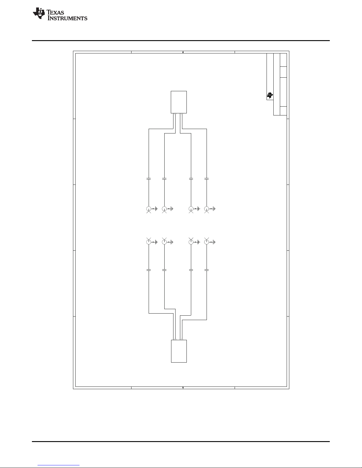
5
5
4
4
3
3
2
2
1
1
D D
C C
B B
A A
B -6519192
HIGH SPEED DIFF SIGNALS
4 28
REV PAGEDOCUMENT NUMBERSIZE
of
TEXAS INSTRUMENTS
PAGE TITLE
C65
0.01uF
TLK60X2
U1-11
RXAPU9RXANU8RXBP
V10
RXBN
V11
C66
0.01uF
J6
RXBP
J5
TXBP
J3
TXAN
J4
RXAN
C68
0.01uF
TLK60X2
U1-10
TXAPV7TXANV6TXBP
U12
TXBN
U13
C69
0.01uF
J8
RXBN
J7
TXBN
C71
0.01uF
C64
0.01uF
C70
0.01uF
J2
RXAP
J1
TXAP
C67
0.01uF
RXBN_SMP
RXBP_SMP
RXAN_SMP
RXAP_SMPTXAP_SMP RXAP
RXAN
RXBP
RXBN
TXBP_SMP
TXBN_SMP
TXAN_SMP
TXBP
TXBN
TXAP
TXAN
NOTE:
SMP CONNECTORS SHOULD BE PLACED ON THE BOTTOM S IDE OF THE BOARD AND THE NETS KEPT AS SHORT AS POSS IBLE.
SERIAL TX AND RX NETS SHOULD MATCH WITHIN 0.5 MIL.
PLACE AC COUPLING CAPACITORS NEAR THE SMP CONN ECTORS.
www.ti.com
TLK6002EVM Schematics
Figure 21. High-Speed Differential, Sheet 4
SLLU132–October 2010 TLK6002 Dual-Channel, 0.47-Gbps to 6.25-Gbps, Multi-Rate Transceiver
Submit Documentation Feedback
Copyright © 2010, Texas Instruments Incorporated
29
Evaluation Module
Page 30
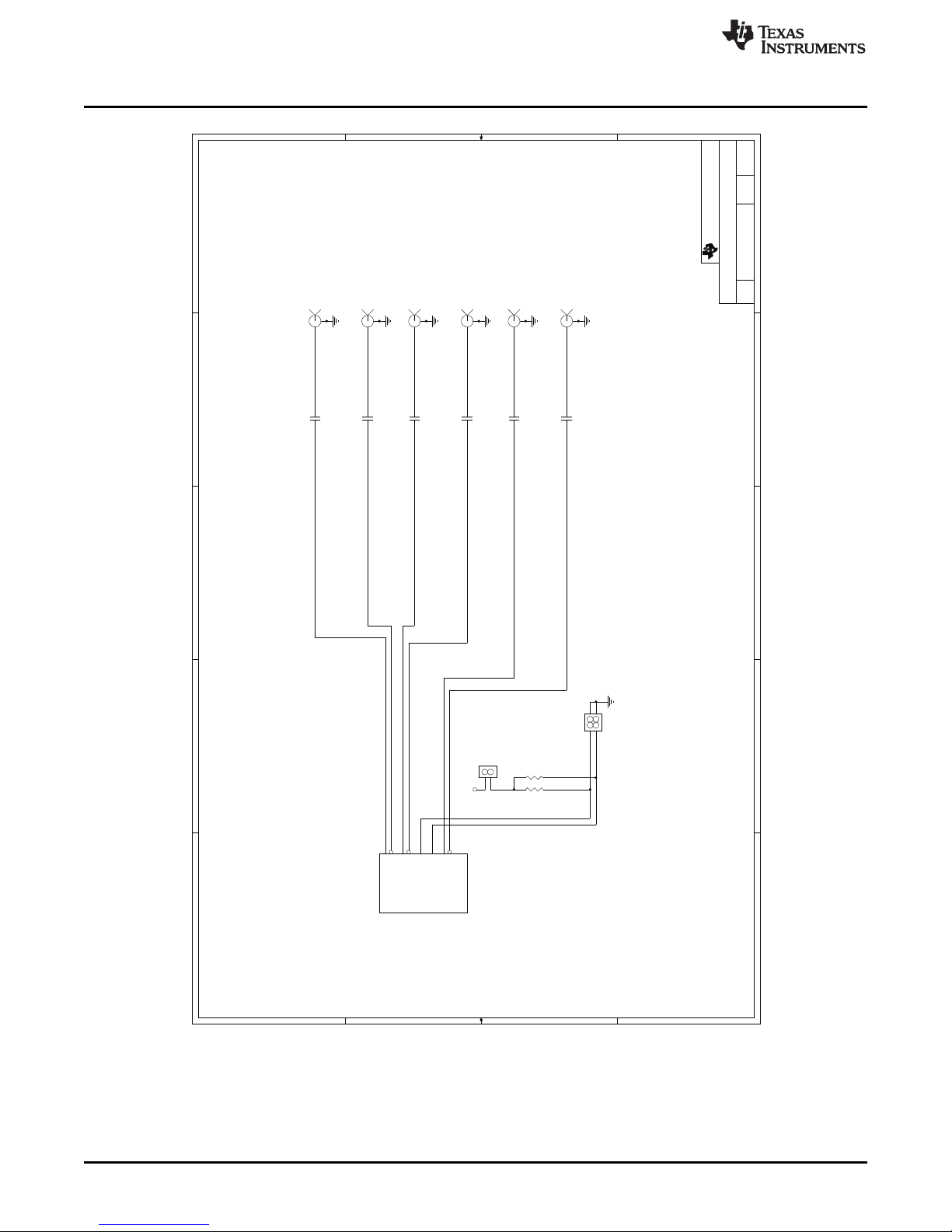
5
5
4
4
3
3
2
2
1
1
D D
C C
B B
A A
B -6519192
REFERENCE CLOCKS / OUTPUT CLOCKS
5 28
REV PAGEDOCUMENT NUMBERSIZE
of
TEXAS INSTRUMENTS
PAGE TITLE
J12
REFCLK0P
TLK60X2
U1-23
REFCLK_0_PB5REFCLK_0_NA5REFCLK_1_PC6REFCLK_1_N
D6
REFCLK_A_SELR6REFCLK_B_SEL
T2
CLK_OUT_PJ6CLK_OUT_N
J7
J10
REFCLK1N
J11
REFCLK0N
JMP29
Header 2x2
1 2
3 4
C75
0.01uF
J14
CLKOUTN
C76
0.01uF
C74
0.01uF
JMP28
PULLUP ENABLE
1
2
C72
0.01uF
R40 4.99K
C77
0.01uF
R41 4.99K
J9
REFCLK1P
J13
CLKOUTP
C73
0.01uF
CLKOUTN_SMP
CLKOUTP
CLKOUTN
REFCLK_SEL_PWR
REFCLK_B_SEL
REFCLK_A_SEL
REFCLK1N
REFCLK1P
REFCLK0N
REFCLK0P
REFCLK0P_SMP
REFCLK0N_SMP
REFCLK1P_SMP
REFCLK1N_SMP
CLKOUTP_SMP
1P5/8V
NOTE:
SMP CONNECTORS SHOULD BE PLACED ON THE BOTTOM S IDE OF THE BOARD AND THE NETS KEPT AS SHORT AS POSS IBLE.
REFCLKP AND REFCLKN AS WELL AS CLOCK_OUT_P AND CLOCK_OUT_N SHO ULD MATCH WITHIN 0.5 MIL.
PLACE AC COUPLING CAPACITORS NEAR THE SMP CONN ECTORS.
TLK6002EVM Schematics
www.ti.com
30
TLK6002 Dual-Channel, 0.47-Gbps to 6.25-Gbps, Multi-Rate Transceiver SLLU132–October 2010
Figure 22. Reference and Output Clocks, Sheet 5
Evaluation Module
Copyright © 2010, Texas Instruments Incorporated
Submit Documentation Feedback
Page 31
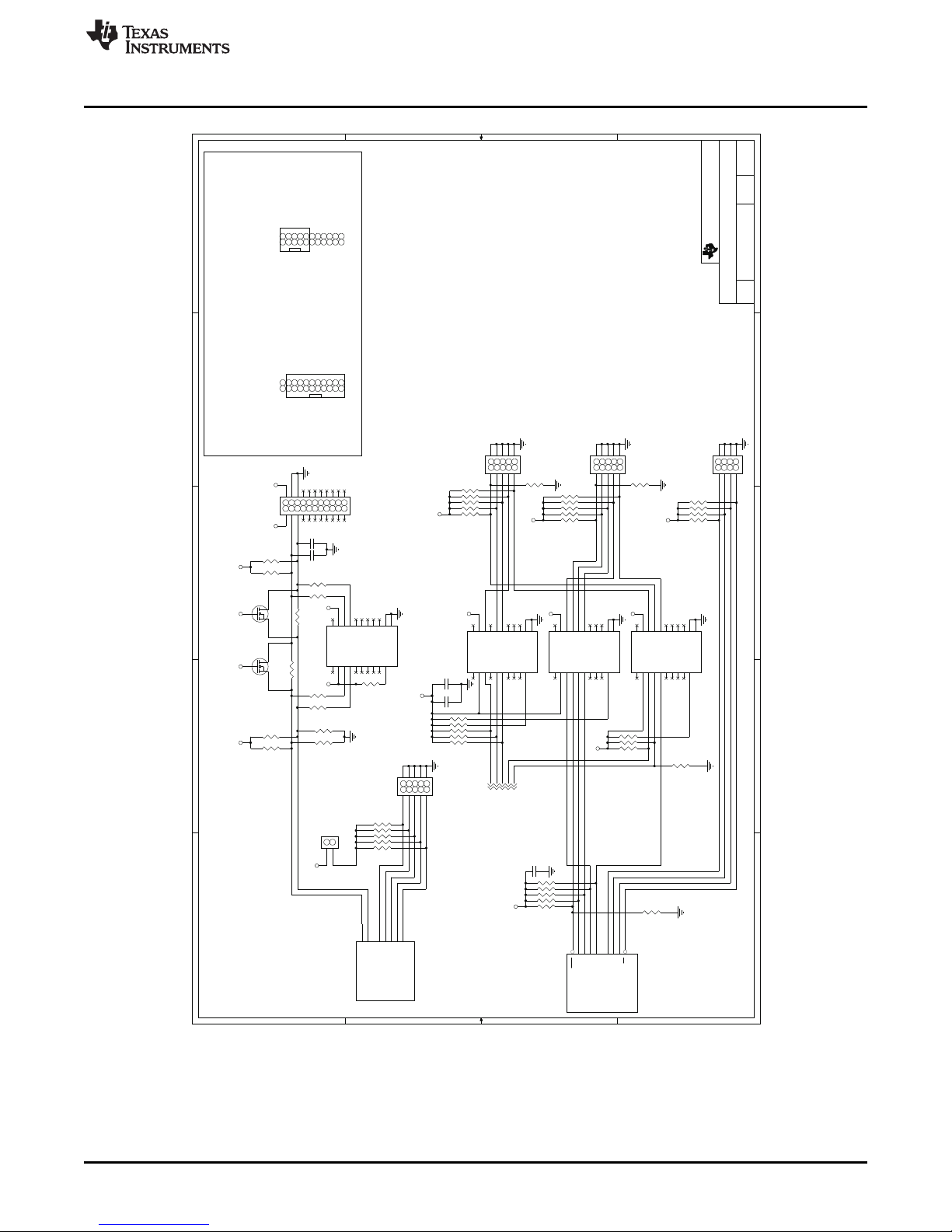
5
5
4
4
3
3
2
2
1
1
D D
C C
B B
A A
B -6519192
JTAG, SPI, I2C, STCI, AND MDIO
6 28
REV PAGEDOCUMENT NUMBERSIZE
of
TEXAS INSTRUMENTS
PAGE TITLE
JMP31
2 Pin Berg Jumper
1
2
R438 4.99K
R44 1.5k
R435 1K
R52 4.99K
R48 4.99K
R450 1K
R49 4.99K
R485 DNI_1K
R531 DNI_0
U84
TXS0108ERGY
A11VCCA2A23A34A45A56A67A78A89OE
10
B1
20
VCCB
19
B218B317B416B515B614B713B8
12
GND
11
GND_PAD
21
R448 1K R432 DNI_1K
R471 1K
TLK60X2
U1-2
TRST
T3
TDO
R14
TDI
R15
TMSR3TCK
T16
SCL
H13
SDO
K13
SDI
E14CSD14
R487 1K
R434 DNI_1K
R455 1K
R486 DNI_1K
R433 DNI_1K
R43 1.5k
R425 1K
R422 4.99K
R489 DNI_1K
U91
TXS0108ERGY
A11VCCA2A23A34A45A56A67A78A89OE
10
B1
20
VCCB
19
B218B317B416B515B614B713B8
12
GND
11
GND_PAD
21
R51 4.99K
R490 DNI_1K
R470 DNI_0
JMP30
MDIO KEYED CONNECTOR
1 2
3 4
5 6
7 8
9 10
11 12
13 14
15 16
17 18
19 20
21 22
R530 DNI_0
R421 DNI_0
U83
TXS0108ERGY
A11VCCA2A23A34A45A56A67A78A89OE
10
B1
20
VCCB
19
B218B317B416B515B614B713B8
12
GND
11
GND_PAD
21
R47 DNI_1.5K
R419 DNI_1K
JMP36
Header 4x2
135
7
246
8
JMP33
Header 5x2
13579
246810
U82
TXS0108ERGY
A11VCCA2A23A34A45A56A67A78A89OE
10
B1
20
VCCB
19
B218B317B416B515B614B713B8
12
GND
11
GND_PAD
21
TLK60X2
U1-3
MDIO
U2
MDC
T1
PRTAD4
V15
PRTAD3M8PRTAD2
K12
PRTAD1
K11
PRTAD0
L11
R45 1.5k
R437 1K
R50 4.99K
C79 DNI
Q1
G
S D
R467 4.99K
C256 2.2uF
R449 1K
C84 2.2uF
R426 DNI_0
Q2
G
S D
C78 DNI
C85
2.2uF
R436 1K
R439 DNI_1K
R447 1K
R488 1K
R42 1.5K
JMP45
Header 5x2
13579
246810
JMP35
Header 5x2
13579
246810
R418 DNI_1K
R46 DNI_1.5K
R532 DNI_0
R424 1K
R420 DNI_1K
R469 DNI_0
R456 1K
R533 DNI_0
R423 1K
R440 DNI_1K
MDIO_CON
MDC
MDIO
PRTAD4
PRTAD3
PRTAD2
PRTAD1
PRTAD0
SCL
SDO
SDI
CS_N
TMS
TDO
SCA
N_LS
_EN
SCANCFG0_LS
SCANCLK_LS
MDC_CON
PRTAD_PWR
TCK
TDI
TRST_N
TRST_N_LS
TDO_LS
TDI_LS
TMS_LS
TCK_LS
SCANOUT_LS
SCANIN_LS
SCANCFG1_LS
1P5/8V
5V1P5/8V
2p5V
3P3V
1P5/8V
3P3V
1P5/8V
1P5/8V
1P5/8V1P5/8V
VDDO3 2p5V
1P5/8V
3P3V
1P5/8V
3P3V
3P3V
SCANCFG0
SCANOUT
SCANIN
SCANCLK
SCANCFG1
GND
GND
MDIO
IF USING A MDIO CONTROLLER THAT
REQUIRES A 20 PIN RIBBON CABLE,
INSTALL THE PCB CONNECTOR ON
PINS 3 THROUGH 22.
43
MDC
GND
GND
MDIO
IF USING A MDIO CONTROLLER THAT
REQUIRES A 10 PIN RIBBON CABLE,
INSTALL THE PCB CONNECTOR ON
PINS 1 THROUGH 10.
21
MDC
21 22
VDD03 5VNCNC
NC
NC
NCNCNCNCNCNCNC
NC NC
NCNCNCNCNCNCNC
9 10
MDIO CONNECTOR (JMP30) INSTALLATION OPTIONS
STCI INTERFACE
MDIO INTERFACE
JTAG INTERFACE
SPI INTERFACE
NOTE: IF MULTIPLE DEVICES ARE CONNECTED TO THE MDIO BUS, RESISTORS R 44
AND R45 MAY NEED TO BE REMOVED IF ADDITIONAL PUL LUP RESISTORS ARE ON THE
BUS ASSOCIATED WITH THE OTHER DEVICES.
IF THE MDIO CONTROLLER USED HAS 1.5V OR 1.8V SIGN AL LEVELS, REMOVE
RESISTORS R530, R531, R532, AND R533 AND INSTALL 0 OHM RESISTORS R46 9
AND R470.
FETS COULD ALSO BE USED AS A LEVEL SHIFTER IF DESI RED AND CAN BE
INSTALLED ON Q1 AND Q2 WITH R469, R470, R530, R531 ,R 532, AND R533
REMOVED.
www.ti.com
TLK6002EVM Schematics
Figure 23. JTAG, SPI, I2C, STCI, and MDIO, Sheet 6
SLLU132–October 2010 TLK6002 Dual-Channel, 0.47-Gbps to 6.25-Gbps, Multi-Rate Transceiver
Submit Documentation Feedback
Copyright © 2010, Texas Instruments Incorporated
31
Evaluation Module
Page 32

5
5
4
4
3
3
2
2
1
1
D D
C C
B B
A A
B -6519192
TD AND RD PARALLEL DATA LINES
7 28
REV PAGEDOCUMENT NUMBERSIZE
of
TEXAS INSTRUMENTS
PAGE TITLE
JMP38B
3
9
15212733394551
57
41016222834404652
58
TLK60X2
U1-8
RDA_19D1RDA_18B3RDA_17B1RDA_16C2RDA_15E2RDA_14F2RDA_13F3RDA_12A2RDA_11C3RDA_10
D3
RDA_9C1RDA_8F4RDA_7D4RDA_6E4RDA_5G4RDA_4G3RDA_3H4RDA_2E5RDA_1H5RDA_0
G5
JMP38A
1
7
13
19
25
31
37
43
49
55
2
8
14
20
26
32
38
44
50
56
JMP37B
3
9
15212733394551
57
41016222834404652
58
JMP40B
3915212733394551
57
4
101622283440465258
JMP39A
1713192531374349
55
2
8
14202632384450
56
JMP39C
5
11
17
23
29
35
41
47
53
59
6
12
18
24
30
36
42
48
54
60
TLK60X2
U1-5
TDA_19H1TDA_18J3TDA_17H2TDA_16K4TDA_15J2TDA_14J1TDA_13K5TDA_12L3TDA_11L5TDA_10M3TDA_9M4TDA_8K3TDA_7M5TDA_6N3TDA_5M2TDA_4P2TDA_3P4TDA_2N5TDA_1R2TDA_0
P5
JMP40C
5
11
17
23
29
35
41
47
53
59
6
12
18
24
30
36
42
48
54
60
TLK60X2
U1-6
TDB_19
J17
TDB_18
H17
TDB_17
J16
TDB_16
H18
TDB_15
K15
TDB_14
K16
TDB_13
L14
TDB_12
L16
TDB_11
M14
TDB_10
M16
TDB_9
M15
TDB_8
P17
TDB_7
N14
TDB_6
N16
TDB_5
J18
TDB_4
M17
TDB_3
R17
TDB_2
P15
TDB_1
P14
TDB_0
P18
JMP37C
5
111723293541475359
61218243036424854
60
JMP38C
5
111723293541475359
61218243036424854
60
JMP37A
1
7
13
19
25
31
37
43
49
55
2
8
14
20
26
32
38
44
50
56
JMP40A
1713192531374349
55
2
8
14202632384450
56
TLK60X2
U1-9
RDB_19
D18
RDB_18
E17
RDB_17
B18
RDB_16
C17
RDB_15
F16
RDB_14
F17
RDB_13
A17
RDB_12
B16
RDB_11
C16
RDB_10
D16
RDB_9
C18
RDB_8
F15
RDB_7
A16
RDB_6
B15
RDB_5
D15
RDB_4
E15
RDB_3
G16
RDB_2
H15
RDB_1
G15
RDB_0
G14
JMP39B
3915212733394551
57
4
101622283440465258
RDA_9
RDA_8
RDA_7
RDA_6
RDA_5
RDA_4
RDA_3
RDA_2
RDA_1
RDA_0
TDA_19
TDA_18
TDA_17
TDA_16
TDA_15
TDA_14
TDA_13
TDA_12
TDA_11
TDA_10
RDB_9
RDB_8
RDB_7
RDB_6
RDB_5
RDB_4
RDB_3
RDB_2
RDB_1
RDB_0
TDB_4
TDB_1
TDB_5
TDB_3
TDB_2
TDB_0
TDB_19
TDB_18
TDB_17
TDB_16
TDB_15
TDB_14
TDB_13
TDB_12
TDB_11
TDB_10
TDB_9
TDB_6
RDB_19
RDB_18
RDB_17
RDB_16
RDB_15
RDB_14
RDB_13
RDB_12
RDB_11
RDB_10
RDA_19
RDA_18
RDA_17
RDA_16
RDA_15
RDA_14
RDA_13
RDA_12
RDA_11
RDA_10
TDA_8
TDA_9
TDA_6
TDA_5
TDA_4
TDA_3
TDA_2
TDA_1
TDA_0
TDA_7
TDB_7
TDB_8
1P5/8V
1P5/8V
GND
6
12
GND
RDA[19:0]
TDA[19:0]54VDD
7
1
TDA[19:0]
49
...
...
NOTE: MATCH THE RD AND TD NET LENGTHS TO WITHIN 0 .5 MILS.
LABEL THE HEADERS ACCORDING TO THE FOLLOWING DIAGRAMS.
56 60
1
7
49
56 60
54
6
12
...
...
1
7
...
49
56
60
54
6
12
... ...
...
GND
6
12
GND
RDB[19:0]
TDB[19:0]54VDD
7
1
TDB[19:0]
49
56 60
(PIN NUMBERS)
(PIN NUMBERS)
(PIN NUMBERS)
(PIN NUMBERS)
TLK6002EVM Schematics
www.ti.com
Figure 24. TD and RD Parallel Data Lines, Sheet 7
32
TLK6002 Dual-Channel, 0.47-Gbps to 6.25-Gbps, Multi-Rate Transceiver SLLU132–October 2010
Evaluation Module
Copyright © 2010, Texas Instruments Incorporated
Submit Documentation Feedback
Page 33

5
5
4
4
3
3
2
2
1
1
D D
C C
B B
A A
B -6519192
TX/RX CLOCKS / A&B CONTROL SIGNALS
8 28
REV PAGEDOCUMENT NUMBERSIZE
of
TEXAS INSTRUMENTS
PAGE TITLE
R37 4.99K
R27 DNI_4.99K
TLK60X2
U1-25
RATE_A2V2RATE_A1T4RATE_A0
U3
CODEA_EN
V4
LOSA
U4
PD_TRXA
T6
PRBSA_PASS
V3
R444 49.9
R443 49.9
JMP25
PULLUP ENABLE
1
2
JMP26
Header 6x2
12
12
3
R34 4.99K
R30 4.99K
R429 DNI_0
R35 4.99K
TLK60X2
U1-7
RXCLK_AF1RXCLK_B
F18
R28 4.99K
TLK60X2
U1-24
RATE_B2
U16
RATE_B1
U17
RATE_B0
U18
CODEB_EN
V16
LOSB
V17
PD_TRXB
U15
PRBSB_PASS
V18
JMP145
Header 4x1
1
R431
DNI_0
R445 20k
JMP27
Header 6x2
12
1 2
3
U5
ZXTD09N50DE6
C11E12C2
3
B2
4
E2
5
B1
6
R29 4.99K
JMP43
Header 2x2
1 2
3 4
D41 HSMB-C170
21
R36 DNI_4.99K
R446 20k
JMP24
PULLUP ENABLE
1
2
R430 DNI_0
JMP146
Header 4x1
1
R31 4.99K
R428 DNI_0
R33 4.99K
R26 4.99K
TLK60X2
U1-4
TXCLK_AP1TXCLK_B
T18
R32 4.99K
D42 HSMB-C170
21
TXCLK_A
TXCLK_BRXCLK_B
RXCLK_A
LOSA_FAIL_LED_BASE
LOSA_FAIL_LED_COL
LOSB_FAIL_LED_COL
LOSB_FAIL_LED_BASE
LOSA
PD_TXRA_N
BCONTROL_PWR
RATE_B1
RATE_B0
CODEB_ENCODEA_EN
ACONTROL_PWR
RATE_A0
RATE_A1
LOSB
RATE_A2
PD_TRXB_N
RATE_B2
5V
5V
1P5/8V 1P5/8V
PRBSB_PASSPRBSA_PASS
SCANIN
SCANCFG0
SCANOUT SCANCFG1
RX/TX CLOCKS
NOTE: MATCH THE RXCLK AND TXCLK NET LENGTHS TO THOSE OF THE RD AND TD NETS WITHIN 0 .5 MILS.
LABEL THE HEADERS ACCORDING TO THE FOLLOWING DIAGRAM.
GND
RXCLK[A:B]
GND
TXCLK[A:B]
www.ti.com
TLK6002EVM Schematics
Figure 25. TX/RX Clocks and A and B Control, Sheet 8
SLLU132–October 2010 TLK6002 Dual-Channel, 0.47-Gbps to 6.25-Gbps, Multi-Rate Transceiver
Submit Documentation Feedback
Copyright © 2010, Texas Instruments Incorporated
33
Evaluation Module
Page 34

5
5
4
4
3
3
2
2
1
1
D D
C C
B B
A A
B -6519192
PRBS PASS/FAIL LEDS
9 28
REV PAGEDOCUMENT NUMBERSIZE
of
TEXAS INSTRUMENTS
PAGE TITLE
R497 4.99K
R501
DNI_0
Q4
G
S D
R39 45.3K
R521 130
R520 45.3K
U86B
SN74LVC112A
1CLK11J31K
2
1Q
5
/1Q
6
/1CLR
15
/1PRE
4
R526 100K
R509
4.99K
R492
4.99K
R494 4.99K
R516 0
R496 0
SW3
Light Touch Switch
125
4
3
U89
TPS3125J18
/RST
1
GND2RST
3
VDD5/MR
4
D50
GREEN
21
R512 4.99K
R519 130
R513 4.99K
Q6
G
S D
U85C
SN74LVC112A
/2PRE102J112CLK132K12/2CLR
14
2Q
9
/2Q
7
R505 4.99K
R514 4.99K
D51
HSMB-C170
21
R25 130D4
GREEN
21
C319
1uF
R491
4.99K
R498 4.99K
U4
ZXTD09N50DE6
C11E12C2
3
B2
4
E2
5
B1
6
R547 0
R556 20K
R38 45.3K
C315 0.1uF
Q5
G
S D
R550 DNI_0
R523 4.99K
R558 20K
R517 4.99K
R499 4.99K
R493 4.99K
R508 100K
SW4
Light Touch Switch
125
4
3
D52
HSMB-C170
21
U92
ZXTD09N50DE6
C11E12C2
3
B2
4
E2
5
B1
6
R495 4.99K
R24 130
U85B
SN74LVC112A
1CLK11J31K
2
1Q
5
/1Q
6
/1CLR
15
/1PRE
4
C316 0.1uF
U86A
SN74LVC112A
VCC
16
GND
8
R524 4.99K
U87
TPS3125J18
/RST
1
GND2RST
3
VDD5/MR
4
R510
4.99K
R522 45.3K
U88
ZXTD09N50DE6
C11E12C2
3
B2
4
E2
5
B1
6
U86C
SN74LVC112A
/2PRE102J112CLK132K12/2CLR
14
2Q
9
/2Q
7
D49
RED
21
D3
RED
21
R511 4.99K
R557 130
C317
4.7uF
R507 49.9
Q3
G
S D
U85A
SN74LVC112A
VCC
16
GND
8
R548 DNI_0
R515 4.99K
R518
DNI_0
R506 4.99K
R549 0
R559 130
R525 49.9
C318
2.2uF
5V
2P5V1P5/8V
2P5V
2P5V
2P5V
1P5/8V 2P5V
5V
1P5/8V
2P5V
2P5V
2P5V
2P5V
5V
2P5V1P5/8V
PRBSB_PASS
PRBSA_PASS
THIS RESISTOR MUX ALLOWS US TO
CONFIGURE THE FETS AS AN INVERTER
OR NON-INVERTER AS WELL AS A
LEVEL TRANSLATOR AND R516 SHOULD
BE REMOVED IF R518 IS INSTALLED
AND R5 REMOVED. THE JK FLIP FLOP
NEEDS CLOCKS ON A HIGH-TO-LOW
EDGE.
THIS RESISTOR MUX ALLOWS US TO
CONFIGURE THE FETS AS AN INVERTER
OR NON-INVERTER AS WELL AS A
LEVEL TRANSLATOR AND R496 SHOULD
BE REMOVED IF R501 IS INSTALLED
AND R5 REMOVED. THE JK FLIP FLOP
NEEDS CLOCKS ON A HIGH-TO-LOW
EDGE.
TLK6002EVM Schematics
www.ti.com
34
TLK6002 Dual-Channel, 0.47-Gbps to 6.25-Gbps, Multi-Rate Transceiver SLLU132–October 2010
Evaluation Module
Figure 26. PRBS Pass/Fail LEDs, Sheet 9
Copyright © 2010, Texas Instruments Incorporated
Submit Documentation Feedback
Page 35

5
5
4
4
3
3
2
2
1
1
D D
C C
B B
A A
B -6519192
1P0V POWER REGULATOR
10 28
REV PAGEDOCUMENT NUMBERSIZE
of
TEXAS INSTRUMENTS
PAGE TITLE
R135 DNI_127
C116 1uF
U13
TPS74401
SS
1
FB
2
OUT3GND
4
IN5BIAS6EN
7
R136
127
SN74CBT3125U14C
2OE42A
5
2B
6
R133 86.6R132 18k
C120
0.001uF
R134 DNI_5.9k
C114 100uF
C117 68uf
+
R127 8.87k
R128 169
R131
8.87k
R137
86.6
C118 10uf
+
JMP55
V_ADJ HEADER
12345
JMP54
DISABLE
1
2
R122 4.99K
SN74CBT3125U14B
1A21OE
1
1B
3
R130
18k
C115 4.7uF
SN74CBT3125U14E
4A124OE
13
4B
11
R129
5.9k
R126
DNI_0
R138
169
C119 1.0uf
R123 1.13k
SN74CBT3125U14D
3OE103A
9
3B
8
SN74CBT3125
U14A
VCC
14
GND
7
R124 0
R125 0
1P0VREG_SS
1P0VREG_EN
1P0VREG_ADJ_MIN
1P0VREG_ADJ_MAN_NOM
1P0VREG_ADJ_MAN_MAX
1P0VREG_ADJ_AUTO_MAX_TRIM
1P0VREG_ADJ_AUTO_NOM_TRIM
1P0VREG_ADJ
1P0VREG_ADJ_MAN_MIN
1P0VREG_ADJ_AUTO_MIN_TRIM
1P0VREG_ADJ_AUTO
1P0VREG_ADJ_MAN_MAX_TRIM
1P0VREG_ADJ_MAN_NOM_TRIM
1P0VREG_ADJ_MAN_MIN_TRIM
1P0VREG_ADJ_AUTO_NOM
1P0VREG_ADJ_AUTO_MAX
1P0VREG_ADJ_AUTO_MIN
1P0VREG_AUTO_EN
1P0V_REG
5V
5V
REG_ENABLE
REG_MAX_ADJ
REG_NOM_ADJ
REG_MIN_ADJ
1.0V REGULATOR
1.0 REGULATOR VOLTAGE MARGIN ADJUSTMENT OPERATION TABLE
V_ADJ REG_MAX_ADJ REG_NOM_ADJ REG_MIN_ADJ
3.0V LOW HIGH HIGH
2.0V HIGH LOW HIGH
1.0V HIGH HIGH LOW
REGULATOR
OUTPUT
1.05V
1.0V
0.95V
X X
X
X X
X X
X X
X
X X
1.05V
0.95V
1.0V
MIN
NOM
MAX
V_ADJ
IF R125 IS INSTALLED AND R126, R134 AND R135 ARE NOT INSTALLED, THE REGULATOR WILL
DEFAULT TO THE TLK6002 MIN VALUE OF 0.95V IF NEITHER REG_ENABLE, REG_MAX_ADJ NOR
REG_NOM_ADJ IS ACTIVE LOW.
IF R126, R134, AND R135 ARE INSTALLED AND R125 IS NOT INSTALLED, THE REGULATOR WILL
NOT DEFAULT TO THE TLK6002 MIN VALUE IF NEITHER REG_ENABLE, REG_MAX_ADJ NOR
REG_NOM_ADJ IS ACTIVE LOW AND WILL REQUIRE AN ACTIVE LOW SIGNAL ON REG_MIN_ADJ TO
SET THE REGULATOR TO THE TLK6002 MIN VALUE. IF NONE OF THESE SIGNALS ARE ACTIVE
LOW, THE REGULATOR WILL DRIFT TO IT'S ABSOLUTE MIN VALUE OF 0.8V AND THE MDIO
REGISTERS SHOULD BE RE-WRITTEN AFTER A VOLTAGE ADJUSTMENT.
R125, R134, AND R135 SHOULD BE INSTALLED OR UNINSTALLED TOGETHER IN ORDER FOR THE
CORRENCT INTENDED OPERATION OF THIS CIRCUIT AND ONLY INSTALLED IF R125 IS
UNINSTALLED.
3.8V HIGH HIGH HIGH 0.0V1,2
SHORT
JMP55 PINS
1,2
1,2
1,2
1,5
1,4
1,3
LOW
REG_ENABLE
HIGH
HIGH
HIGH
X
X
X
www.ti.com
TLK6002EVM Schematics
Figure 27. 1p0V Power Regulator, Sheet 10
SLLU132–October 2010 TLK6002 Dual-Channel, 0.47-Gbps to 6.25-Gbps, Multi-Rate Transceiver
Submit Documentation Feedback
Copyright © 2010, Texas Instruments Incorporated
Evaluation Module
35
Page 36

5
5
4
4
3
3
2
2
1
1
D D
C C
B B
A A
B -6519192
1P2V POWER REGULATOR
11 28
REV PAGEDOCUMENT NUMBERSIZE
of
TEXAS INSTRUMENTS
PAGE TITLE
R110 16.5K
U69
TPS74401
SS
1
FB
2
OUT3GND
4
IN5BIAS6EN
7
R107 0
C113
0.001uF
R120
665
C112 1.0uf
JMP53
V_ADJ HEADER
12345
R116 665
R114
16.5K
C108 4.7uF
SN74CBT3125U12C
2OE42A
5
2B
6
R113
32.4K
R106 2.49K
R121
66.5
C110 68uf
+
SN74CBT3125U12B
1A21OE
1
1B
3
R112
5.62K
R118 DNI_243
C111 10uf
+
JMP52
DISABLE
1
2
C109 1uF
R108 0
R109
DNI_0
R115 32.4K
SN74CBT3125U12D
3OE103A
9
3B
8
R111 66.5
R105 4.99K
SN74CBT3125U12E
4A124OE
13
4B
11
R119
243
SN74CBT3125
U12A
VCC
14
GND
7
R117 DNI_5.62K
C107 100uF
1P2VREG_SS
1P2VREG_EN
1P2VREG_ADJ_MIN
1P2VREG_ADJ_MAN_NOM
1P2VREG_ADJ_MAN_MAX
1P2VREG_ADJ_AUTO_NOM_TRIM
1P2VREG_ADJ_AUTO_MAX_TRIM
1P2VREG1-_ADJ_AUTO_MIN_TRIM
1P2VREG_ADJ_AUTO 1P2VREG_ADJ
1P2VREG_ADJ_MAN_MIN
1P2VREG_ADJ_MAN_NOM_TRIM
1P2VREG_ADJ_MAN_MAX_TRIM
1P2VREG_ADJ_MAN_MIN_TRIM
1P2VREG_ADJ_AUTO_MAX
1P2VREG_ADJ_AUTO_NOM
1P2VREG_ADJ_AUTO_MIN
1P2VREG_AUTO_EN
1P2V_REG
5V
5V
REG_ENABLE
REG_MAX_ADJ
REG_NOM_ADJ
REG_MIN_ADJ
1.2V REGULATOR
MIN
NOM
MAX
V_ADJ
IF R108 IS INSTALLED AND R109, R117 AND R118 ARE NOT INSTALLED, THE REGULATOR WILL
DEFAULT TO THE TLK6002 MIN VALUE OF 1.14V IF NEITHER REG_ENABLE, REG_MAX_ADJ NOR
REG_NOM_ADJ IS ACTIVE LOW.
IF R108, R117, AND R118 ARE INSTALLED AND R108 IS NOT INSTALLED, THE REGULATOR
WILL NOT DEFAULT TO THE TLK6002 MIN VALUE IF NEITHER REG_ENABLE, REG_MAX_ADJ NOR
REG_NOM_ADJ IS ACTIVE LOW AND WILL REQUIRE AN ACTIVE LOW SIGNAL ON REG_MIN_ADJ TO
SET THE REGULATOR TO THE TLK6002 MIN VALUE. IF NONE OF THESE SIGNALS ARE ACTIVE
LOW, THE REGULATOR WILL DRIFT TO IT'S ABSOLUTE MIN VALUE OF 0.8V AND THE MDIO
REGISTERS SHOULD BE RE-WRITTEN AFTER A VOLTAGE ADJUSTMENT.
R109, R117, AND R118 SHOULD BE INSTALLED OR UNINSTALLED TOGETHER IN ORDER FOR THE
CORRENCT INTENDED OPERATION OF THIS CIRCUIT AND ONLY INSTALLED IF R108 IS
UNINSTALLED.
3.8V HIGH HIGH HIGH 0.0V1,2
SHORT
JMP53 PINS
1,2
1,2
1,2
1,5
1,4
1,3
LOW
REG_ENABLE
HIGH
HIGH
HIGH
X
X
X
1.2V REGULATOR VOLTAGE MARGIN ADJUSTMENT OPERATION TABLE
V_ADJ REG_MAX_ADJ REG_NOM_ADJ REG_MIN_ADJ
3.0V LOW HIGH HIGH
2.0V HIGH LOW HIGH
1.0V HIGH HIGH LOW
REGULATOR
OUTPUT
1.26V
1.2V
1.14V
X X
X
X X
X X
X X
X
X X
1.26V
1.14V
1.2V
TLK6002EVM Schematics
www.ti.com
Figure 28. 1p2V Power Regulator, Sheet 11
36
TLK6002 Dual-Channel, 0.47-Gbps to 6.25-Gbps, Multi-Rate Transceiver SLLU132–October 2010
Evaluation Module
Copyright © 2010, Texas Instruments Incorporated
Submit Documentation Feedback
Page 37

5
5
4
4
3
3
2
2
1
1
D D
C C
B B
A A
B -6519192
1P5V POWER REGULATOR
12 28
REV PAGEDOCUMENT NUMBERSIZE
of
TEXAS INSTRUMENTS
PAGE TITLE
C93 100uF
C97 10uf
+
R78 32.4K
R86
576
R79 576
C98 1.0uf
R83 DNI_5.36K
U8
TPS74401
SS
1
FB
2
OUT3GND
4
IN5BIAS6EN
7
R87
280
SN74CBT3125U9C
2OE42A
5
2B
6
R73 0
R75
DNI_0
R77 280
SN74CBT3125U9E
4A124OE
13
4B
11
C95 1uF
JMP49
V_ADJ HEADER
12345
C99
0.001uF
SN74CBT3125U9A
VCC
14
GND
7
R72 4.12K
R71 4.99K
JMP48
DISABLE
1
2
R80
5.36K
C94 4.7uF
SN74CBT3125U9D
3OE103A
9
3B
8
C96 68uf
+
R76 16.2K
R84 DNI_133
SN74CBT3125U9B
1A21OE
1
1B
3
R81
32.4K
R74 0
R82
16.2K
R85
133
1P5VREG_SS
1P5VREG_ADJ_MIN
1P5VREG_ADJ_MAN_NOM
1P5VREG_ADJ_MAN_MAX
1P5VREG_EN_ADJ1P5VREG_ADJ_AUTO
1P5VREG_ADJ_MAN_MIN
1P5VREG_ADJ_MIN_TRIM
1P5VREG_ADJ_NOM_TRIM
1P5VREG_ADJ_MAX_TRIM
1P5VREG_ADJ_AUTO_MAX 1P5VREG_ADJ_AUTO_MAX_TRIM
1P5VREG_ADJ_AUTO_NOM 1P5 VREG_ADJ_AUTO_NOM_TRIM
1P5VREG_ADJ_AUTO_MIN 1P5VREG_ADJ_AUTO_MIN_TRIM
1P5VREG_EN
1P5VREG_AUTO_EN
1P5V_REG
5V
5V
REG_ENABLE
REG_MAX_ADJ
REG_NOM_ADJ
REG_MIN_ADJ
1.5V REGULATOR
MIN
NOM
MAX
V_ADJ
IF R74 IS INSTALLED AND R75, R83, AND R84 ARE NOT INSTALLED, THE REGULATOR WILL
DEFAULT TO THE TLK6002 MIN VALUE OF 1.4V IF NEITHER REG_ENABLE, REG_MAX_ADJ NOR
REG_NOM_ADJ IS ACTIVE LOW.
IF R75, R83, AND R84 ARE INSTALLED AND R74 IS NOT INSTALLED, THE REGULATOR WILL NOT
DEFAULT TO THE TLK6002 MIN VALUE IF NEITHER REG_ENABLE, REG_MAX_ADJ NOR REG_NOM_ADJ
IS ACTIVE LOW AND WILL REQUIRE AN ACTIVE LOW SIGNAL ON REG_MIN_ADJ TO SET THE
REGULATOR TO THE TLK6002 MIN VALUE. IF NONE OF THESE SIGNALS ARE ACTIVE LOW, THE
REGULATOR WILL DRIFT TO IT'S ABSOLUTE MIN VALUE OF 0.8V AND THE MDIO REGISTERS
SHOULD BE RE-WRITTEN AFTER A VOLTAGE ADJUSTMENT.
R75, R83, AND R84 SHOULD BE INSTALLED OR UNINSTALLED TOGETHER IN ORDER FOR THE
CORRENCT INTENDED OPERATION OF THIS CIRCUIT AND ONLY INSTALLED IF R74 IS
UNINSTALLED.
3.8V HIGH HIGH HIGH 0.0V1,2
SHORT
JMP49 PINS
1,2
1,2
1,2
1,5
1,4
1,3
LOW
REG_ENABLE
HIGH
HIGH
HIGH
X
X
X
1.5V REGULATOR VOLTAGE MARGIN ADJUSTMENT OPERATION TABLE
V_ADJ REG_MAX_ADJ REG_NOM_ADJ REG_MIN_ADJ
3.0V LOW HIGH HIGH
2.0V HIGH LOW HIGH
1.0V HIGH HIGH LOW
REGULATOR
OUTPUT
1.6V
1.5V
1.4V
X X
X
X X
X X
X X
X
X X
1.6V
1.4V
1.5V
www.ti.com
TLK6002EVM Schematics
Figure 29. 1p5V Power Regulator, Sheet 12
SLLU132–October 2010 TLK6002 Dual-Channel, 0.47-Gbps to 6.25-Gbps, Multi-Rate Transceiver
Submit Documentation Feedback
Copyright © 2010, Texas Instruments Incorporated
Evaluation Module
37
Page 38

5
5
4
4
3
3
2
2
1
1
D D
C C
B B
A A
B -6519192
1P8V POWER REGULATOR
13 28
REV PAGEDOCUMENT NUMBERSIZE
of
TEXAS INSTRUMENTS
PAGE TITLES N74CBT3125U11A
VCC
14
GND
7
R92
DNI_0
R95
3.09K
JMP50
DISABLE
1
2
C104 10uf
+
R91 0
SN74CBT3125U11D
3OE103A
9
3B
8
R104
294
R98 28K
C100 100uF
U10
TPS74401
SS
1
FB
2
OUT3GND
4
IN5BIAS6EN
7
R94 294
SN74CBT3125U11E
4A124OE
13
4B
11
R102
82.5
R97
14K
R100 DNI_3.09K
R90 0
R88 4.99K
R99 619
R89 3.57K
C101 4.7uF
JMP51
V_ADJ HEADER
12345
SN74CBT3125U11B
1A21OE
1
1B
3
C105 1.0uf
R101 DNI_82.5
C103 68uf
+
C106
0.001uF
SN74CBT3125U11C
2OE42A
5
2B
6
C102 1uF
R93 14K
R96
28K
R103
619
1P8VREG_SS
1P8VREG_EN
1P8VREG_ADJ_MIN
1P8VREG_ADJ_MAN_NOM
1P8VREG_ADJ_MAN_MAX
1P8VREG_ADJ_AUTO_MAX_TRIM
1P8VREG_ADJ_AUTO_NOM_TRIM
1P8VREG_ADJ
1P8VREG_ADJ_AUTO_MIN_TRIM
1P8VREG_ADJ_AUTO
1P8VREG_ADJ_MAN_MIN
1P8VREG_ADJ_MAN_MIN_TRIM
1P8VREG_ADJ_MAN_NOM_TRIM
1P8VREG_ADJ_MAN_MAX_TRIM
1P8VREG_ADJ_AUTO_NOM
1P8VREG_ADJ_AUTO_MIN
1P8VREG_ADJ_AUTO_MAX
1P8VREG_AUTO_EN
1P8V_REG
5V
5V
REG_ENABLE
REG_MAX_ADJ
REG_NOM_ADJ
REG_MIN_ADJ
1.8V REGULATOR
MIN
NOM
MAX
V_ADJ
IF R91 IS INSTALLED AND R92, R100, AND R101 ARE NOT INSTALLED, THE REGULATOR WILL
DEFAULT TO THE TLK6002 MIN VALUE OF 1.7V IF NEITHER REG_ENABLE, REG_MAX_ADJ NOR
REG_NOM_ADJ IS ACTIVE LOW.
IF R92, R100, AND R101 ARE INSTALLED AND R91 IS NOT INSTALLED, THE REGULATOR WILL
NOT DEFAULT TO THE TLK6002 MIN VALUE IF NEITHER REG_ENABLE, REG_MAX_ADJ NOR
REG_NOM_ADJ IS ACTIVE LOW AND WILL REQUIRE AN ACTIVE LOW SIGNAL ON REG_MIN_ADJ TO
SET THE REGULATOR TO THE TLK6002 MIN VALUE. IF NONE OF THESE SIGNALS ARE ACTIVE
LOW, THE REGULATOR WILL DRIFT TO IT'S ABSOLUTE MIN VALUE OF 0.8V AND THE MDIO
REGISTERS MUST BE RE-WRITTEN AFTER A VOLTAGE ADJUSTMENT.
R92, R100, AND R101 SHOULD BE INSTALLED OR UNINSTALLED TOGETHER IN ORDER FOR THE
CORRENCT INTENDED OPERATION OF THIS CIRCUIT AND ONLY INSTALLED IF R91 IS
UNINSTALLED.
3.8V HIGH HIGH HIGH 0.0V1,2
SHORT
JMP51 PINS
1,2
1,2
1,2
1,5
1,4
1,3
LOW
REG_ENABLE
HIGH
HIGH
HIGH
X
X
X
1.8V REGULATOR VOLTAGE MARGIN ADJUSTMENT OPERATION TABLE
V_ADJ REG_MAX_ADJ REG_NOM_ADJ REG_MIN_ADJ
3.0V LOW HIGH HIGH
2.0V HIGH LOW HIGH
1.0V HIGH HIGH LOW
REGULATOR
OUTPUT
1.9V
1.8V
1.7V
X X
X
X X
X X
X X
X
X X
1.9V
1.7V
1.8V
TLK6002EVM Schematics
www.ti.com
Figure 30. 1p8V Power Regulator, Sheet 13
38
TLK6002 Dual-Channel, 0.47-Gbps to 6.25-Gbps, Multi-Rate Transceiver SLLU132–October 2010
Evaluation Module
Copyright © 2010, Texas Instruments Incorporated
Submit Documentation Feedback
Page 39

5
5
4
4
3
3
2
2
1
1
D D
C C
B B
A A
B -6519192
2P5V POWER REGULATOR
14 28
REV PAGEDOCUMENT NUMBERSIZE
of
TEXAS INSTRUMENTS
PAGE TITLE
C87 4.7uF
U6
TPS74401
SS
1
FB
2
OUT3GND
4
IN5BIAS6EN
7
R66 DNI_130
R61 340
SN74CBT3125U7C
2OE42A
5
2B
6
R60 10.5KR59 453
R70
453
R63
1.69K
R69
340
C91 1.0uf
R68
130
R58
DNI_0
R67 DNI_1.69K
R56 0
SN74CBT3125U7A
VCC
14
GND
7
C86 100uF
R54 4.99K
C89 68uf
+
JMP47
V_ADJ HEADER
12345
SN74CBT3125U7D
3OE103A
9
3B
8
R65
10.5K
C92
0.001uF
R64
21.5K
C90 10uf
+
R57 0
JMP46
DISABLE
1
2
SN74CBT3125U7B
1A21OE
1
1B
3
SN74CBT3125U7E
4A124OE
13
4B
11
R55 3.57K
R62 21.5K
C88 1uF
2P5VREG_SS
2P5VREG_ADJ_MIN
2P5VREG_ADJ_MAN_NOM
2P5VREG_ADJ_MAN_MAX
2P5VREG_ADJ
2P5VREG_ADJ_MAN_MIN
2P5VREG_ADJ_AUTO
2P5VREG_ADJ_MAN_MAX_TRIM
2P5VREG_ADJ_MAN_NOM_TRIM
2P5VREG_ADJ_MAN_MIN_TRIM
2P5VREG_ADJ_AUTO_MIN
2P5VREG_ADJ_AUTO_NOM
2P5VREG_ADJ_AUTO_MAX 2P5VREG_ADJ_AUTO_MAX_TRIM
2P5VREG_ADJ_AUTO_NOM_TRIM
2P5VREG_ADJ_AUTO_MIN_TRIM
2P5VREG_EN
2P5VREG_AUTO_EN
2P5V_REG5V
5V
REG_ENABLE
REG_MAX_ADJ
REG_NOM_ADJ
REG_MIN_ADJ
2.5V REGULATOR
MAX
NOM
MIN
V_ADJ
IF R57 IS INSTALLED AND R58,R66, AND R67 ARE NOT INSTALLED, THE REGULATOR WILL
DEFAULT TO THE TLK6002 MIN VALUE OF 2.37V IF NEITHER REG_ENABLE, REG_MAX_ADJ NOR
REG_NOM_ADJ IS ACTIVE LOW.
IF R58,R66, AND R67 ARE INSTALLED AND R57 IS NOT INSTALLED, THE REGULATOR WILL NOT
DEFAULT TO THE TLK6002 MIN VALUE IF NEITHER REG_ENABLE, REG_MAX_ADJ NOR REG_NOM_ADJ
IS ACTIVE LOW AND WILL REQUIRE AN ACTIVE LOW SIGNAL ON REG_MIN_ADJ TO SET THE
REGULATOR TO THE TLK6002 MIN VALUE OF 2.37V. IF NONE OF THESE SIGNALS ARE ACTIVE
LOW, THE REGULATOR WILL DRIFT TO IT'S ABSOLUTE MIN VALUE OF 0.8V AND THE MDIO
REGISTERS MUST BE RE-WRITTEN AFTER A VOLTAGE ADJUSTMENT.
R58, R66, AND R67 SHOULD BE INSTALLED OR UNINSTALLED TOGETHER IN ORDER FOR THE
CORRENCT INTENDED OPERATION OF THIS CIRCUIT AND ONLY INSTALLED IF R57 IS
UNINSTALLED.
3.8V HIGH HIGH HIGH 0.0V1,2
SHORT
JMP47 PINS
1,2
1,2
1,2
1,5
1,4
1,3
LOW
REG_ENABLE
HIGH
HIGH
HIGH
XXX
2.5V REGULATOR VOLTAGE MARGIN ADJUSTMENT OPERATION TABLE
V_ADJ REG_MAX_ADJ REG_NOM_ADJ REG_MIN_ADJ
3.0V LOW HIGH HIGH
2.0V HIGH LOW HIGH
1.0V HIGH HIGH LOW
REGULATOR
OUTPUT
2.63V
2.5V
2.37V
X X
X
X X
X X
X X
X
X X
2.63V
2.37V
2.5V
www.ti.com
TLK6002EVM Schematics
Figure 31. 2p5V Power Regulator, Sheet 14
SLLU132–October 2010 TLK6002 Dual-Channel, 0.47-Gbps to 6.25-Gbps, Multi-Rate Transceiver
Submit Documentation Feedback
Copyright © 2010, Texas Instruments Incorporated
Evaluation Module
39
Page 40

5
5
4
4
3
3
2
2
1
1
D D
C C
B B
A A
B -6519192
3P3V POWER REGULATOR
15 28
REV PAGEDOCUMENT NUMBERSIZE
of
TEXAS INSTRUMENTS
PAGE TITLE
SN74CBT3125U67B
1A21OE
1
1B
3
C235 4.7uF
R368 200
R378
200
R363 3.57K
R377
392
C236 1uF
R376
23.2
SN74CBT3125U67D
3OE103A
9
3B
8
C240
0.001uF
R375 DNI_23.2
C238 10uf
+
SN74CBT3125U67A
VCC
14
GND
7
R374 DNI_1.2k
JMP147
DISABLE
1
2
R362 4.99K
SN74CBT3125U67C
2OE42A
5
2B
6
R367 8.45k
SN74CBT3125U67E
4A124OE
13
4B
11
R371
1.2k
JMP148
V_ADJ HEADER
12345
R370 392
C239 1.0uf
R373
8.45k
R366
DNI_0
R372
16.9k
R364 0
U70
TPS74401
SS
1
FB
2
OUT3GND
4
IN5BIAS6EN
7
R365 0
C234 100uF
R369 16.9k
C237 68uf
+
3P3VREG_SS
3P3VREG_ADJ_MIN
3P3VREG_ADJ_MAN_NOM
3P3VREG_ADJ_MAN_MAX
3P3VREG_ADJ
3P3VREG_ADJ_MAN_MIN
3P3VREG_ADJ_AUTO
3P3VREG_ADJ_MAN_MAX_TRIM
3P3VREG_ADJ_MAN_NOM_TRIM
3P3VREG_ADJ_MAN_MIN_TRIM
3P3VREG_ADJ_AUTO_MIN
3P3VREG_ADJ_AUTO_NOM
3P3VREG_ADJ_AUTO_MAX 3P3VREG_ADJ_AUTO_MAX_TRIM
3P3VREG_ADJ_AUTO_NOM_TRIM
3P3VREG_ADJ_AUTO_MIN_TRIM
3P3VREG_EN
3P3VREG_AUTO_EN
3P3V_REG5V
5V
REG_ENABLE
REG_MAX_ADJ
REG_NOM_ADJ
REG_MIN_ADJ
3.3V REGULATOR
MAX
NOM
MIN
V_ADJ
IF R365 IS INSTALLED AND R366,R374, AND R375 ARE NOT INSTALLED, THE REGULATOR WILL
DEFAULT TO THE TLK6002 MIN VALUE OF 3.135V IF NEITHER REG_ENABLE, REG_MAX_ADJ NOR
REG_NOM_ADJ IS ACTIVE LOW.
IF R366,R374,AND R375 ARE INSTALLED AND R365 IS NOT INSTALLED,THE REGULATOR WILL NOT
DEFAULT TO THE TLK6002 MIN VALUE IF NEITHER REG_ENABLE, REG_MAX_ADJ NOR REG_NOM_ADJ
IS ACTIVE LOW AND WILL REQUIRE AN ACTIVE LOW SIGNAL ON REG_MIN_ADJ TO SET THE
REGULATOR TO THE TLK6002 MIN VALUE OF 3.135V. IF NONE OF THESE SIGNALS ARE ACTIVE
LOW, THE REGULATOR WILL DRIFT TO IT'S ABSOLUTE MIN VALUE OF 0.8V AND THE MDIO
REGISTERS MUST BE RE-WRITTEN AFTER A VOLTAGE ADJUSTMENT.
R366, R374, AND R375 SHOULD BE INSTALLED OR UNINSTALLED TOGETHER IN ORDER FOR THE
CORRENCT INTENDED OPERATION OF THIS CIRCUIT AND ONLY INSTALLED IF R365 IS
UNINSTALLED.
3.8V HIGH HIGH HIGH 0.0V1,2
SHORT
JMP148 PINS
1,2
1,2
1,2
1,5
1,4
1,3
LOW
REG_ENABLE
HIGH
HIGH
HIGH
X
X
X
3.3V REGULATOR VOLTAGE MARGIN ADJUSTMENT OPERATION TABLE
V_ADJ REG_MAX_ADJ REG_NOM_ADJ REG_MIN_ADJ
3.0V LOW HIGH HIGH
2.0V HIGH LOW HIGH
1.0V HIGH HIGH LOW
REGULATOR
OUTPUT
3.465V
3.3V
3.135V
X X
X
X X
X X
X X
X
X X
3.465
3.135V
3.3V
TLK6002EVM Schematics
www.ti.com
Figure 32. 3p3V Power Regulator, Sheet 15
40
TLK6002 Dual-Channel, 0.47-Gbps to 6.25-Gbps, Multi-Rate Transceiver SLLU132–October 2010
Evaluation Module
Copyright © 2010, Texas Instruments Incorporated
Submit Documentation Feedback
Page 41

5
5
4
4
3
3
2
2
1
1
D D
C C
B B
A A
B -6519192
POWER REGULATOR MIN/NOM/MAX ADJUSTME NT
16 28
REV PAGEDOCUMENT NUMBERSIZE
of
TEXAS INSTRUMENTS
PAGE TITLE
R158 30.83K
U19C CD4025B
D3E4F
5
K
6
C121
0.47uF
R161
6.65K
CD4011BU 18E
G12H
13
M
11
R142 10.0K
R157 5.6K
JMP57
V_ADJ HEADER
12345
R159
4.99K
LM339AU16D
3 IN_N83 IN_P
9
3 OUT
14
-
+
U17D CD4025B
G13H12I
11
L
10
LM339AU16A
VCC
3
GND
12
R160
15K
U17C CD4025B
D3E4F
5
K
6
R141
919
R153
2.87K
LM339AU20A
VCC
3
GND
12
CD4011BU 18C
D6C
5
K
4
CD4011BU18A
VDD
14
VSS
7
U19D CD4025B
G13H12I
11
L
10
R154
10.5K
R143 3.09K
U17A CD4025B
VDD
14
VSS
7
LM339AU20D
3 IN_N83 IN_P
9
3 OUT
14
-
+
JMP56
ENABLE
123
LM339AU16E
4 IN_P114 IN_N
10
4 OUT
13
-
+
CD4011BU 18D
F9E
8
L
10
U19B CD4025B
A1B2C
8
J
9
CD4011BU 18B
A1B
2
J
3
R150
1.27K
R146 10K
U19A CD4025B
VDD
14
VSS
7
LM339AU16B
1 IN_P71 IN_N
6
1 OUT
1
-
+
R140
4.99K
R162 10.0K
U15
REF2940
VIN
1
VOUT
2
GND
3
R151 10.5K
R152
4.99K
P1
V_ADJ_BJ
1
R148 10.0K
R144
4.99K
R139 0
R147
3.3K
LM339AU16C
2 IN_N42 IN_P
5
2 OUT
2
-
+
LM339AU20B
1 IN_P71 IN_N
6
1 OUT
1
-
+
LM339AU20E
4 IN_P114 IN_N
10
4 OUT
13
-
+
R155 10.0K
LM339AU20C
2 IN_N42 IN_P
5
2 OUT
2
-
+
R149 100
R145
1.82K
U17B CD4025B
A1B2C
8
J
9
R156
10.0K
V_ADJ_NOM_VREF_LOW
V_ADJ_MAX
V_ADJ_NOM_VREF_HIGH
VADJ_ENABLE_VREF_HIGH
VADJ_4V
VADJ_ENABLE_VREF_LOW
V_ADJ_MIN_VREF_HIGH
V_ADJ_MIN_VREF_LOW
V_ADJ_MAX_VREF_HIGH
V_ADJ_EN
V_ADJ_MIN
V_ADJ_MAX_VREF_LOW
V_ADJ_MIN_NOR
VADJ_3V
V_ADJ_NOM
V_ADJ_EN_NOR
V_ADJ_MAX_NOR
VADJ_BJ
V_ADJ_NOM_NOR
VADJ_2V
VADJ_1V
VADJ_NORM
5V
4P096V_REF0
5V
5V
5V
5V
V_ADJ
5V
5V
5V
5V
5V
REG_ENABLE
REG_MAX_ADJ
REG_NOM_ADJ
REG_MIN_ADJ
VOLTAGE REGULATOR MARGIN ADJUSTMENT
CONTROL SIGNAL OPERATION TABLE
PRECISION VOLTAGE
REFERENCE = 4.096V
3.25V
2.75V
2.25V
1.75V
1.25V
0.75V
V_ADJ_MAX = HIGH FOR
2.75V < V_ADJ < 3.25V ELSE
V_ADJ_MAX = LOW
V_ADJ_EN = HIGH FOR
3.75V < V_ADJ < 4.096V ELSE
V_ADJ_EN = LOW
DISABLE=3.8V
V_ADJ_NOM= HIGH FOR
1.75V < V_ADJ < 2.25V ELSE
V_ADJ_NOM = LOW
V_ADJ_MIN = HIGH FOR
0.75V < V_ADJ < 1.25V ELSE
V_ADJ_MAX = LOW
V_ADJ REG_MAX_ADJ REG_NOM_ADJ REG_MIN_ADJ
3.0V LOW HIGH HIGH
4.096V
3.75V
2.0V HIGH LOW HIGH
1.0V HIGH HIGH LOW
MIN=1V
NOM=2V
MAX=3V
V_ADJ_BJ
3.8V HIGH HIGH HIGH
REG_ENABLE
HIGH
HIGH
HIGH
LOW
www.ti.com
TLK6002EVM Schematics
SLLU132–October 2010 TLK6002 Dual-Channel, 0.47-Gbps to 6.25-Gbps, Multi-Rate Transceiver
Submit Documentation Feedback
Figure 33. Power Regulator Min/Nom/Max Adjustment, Sheet 16
Copyright © 2010, Texas Instruments Incorporated
41
Evaluation Module
Page 42
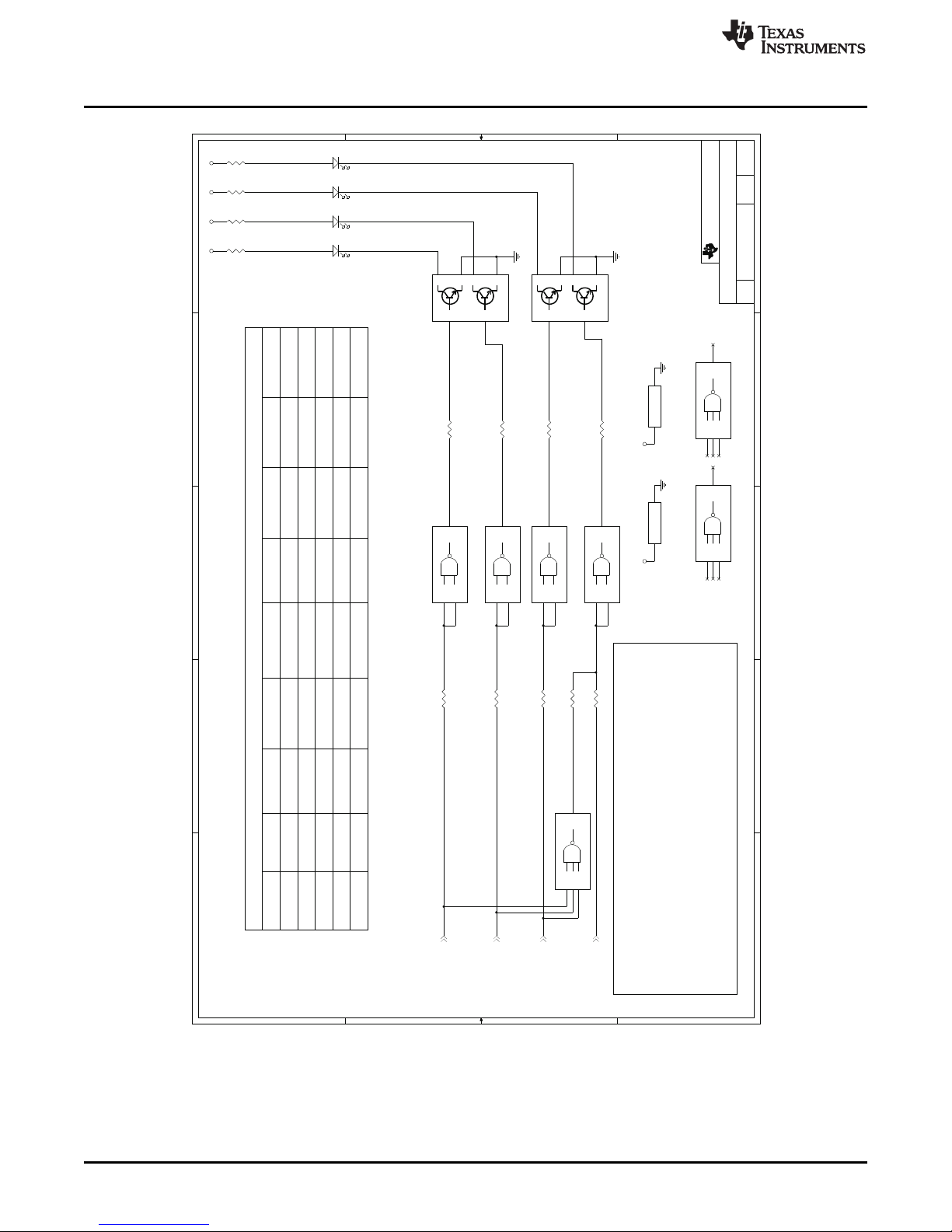
5
5
4
4
3
3
2
2
1
1
D D
C C
B B
A A
B -6519192
POWER REG MIN/NOM/MAX ADJUSTMENT LED S
17 28
REV PAGEDOCUMENT NUMBERSIZE
of
TEXAS INSTRUMENTS
PAGE TITLE
U24D CD4023B
G13H12I
11
L
10
D5
HSMS-C170
21
CD4011BU 21D
F9E
8
L
10
R165
49.9
R172 105K
R166
130
CD4011BU21A
VDD
14
VSS
7
R170 105K
R164
130
R167 0
U24C CD4023B
D3E4F
5
K
6
CD4011BU 21E
G12H
13
M
11
U24B CD4023B
A1B2C
8
J
9
R169 0
R168 105K
U22
ZXTD09N50DE6
C11E12C2
3
B2
4
E2
5
B1
6
U23
ZXTD09N50DE6
C11E12C2
3
B2
4
E2
5
B1
6
D6
HSMG-C170
21
U24A CD4023B
VDD
14
VSS
7
R163
130
R171 0
R175 105K
R174 DNI_0
CD4011BU 21C
D6C
5
K
4
R173 0
D7
HSMB-C170
21
CD4011BU 21B
A1B
2
J
3
D8
HSMY-C170
21
REG_ADJ_MIN_DEFAULT_LED
INV_REG_ADJ_EN_LED REG_ADJ_EN_LED_BASE
REG_ADJ_EN_LED
REG_ADJ_NOM_LED_BASEINV_REG_ADJ_NOM_LED
INV_REG_ADJ_MIN_LED
REG_ADJ_EN_LED_COL
REG_ADJ_MAX_LED_COL
REG_ADJ_MIN_LED_COL
REG_ADJ_EN_LED_VF
REG_ADJ_MAX_LED_VF
REG_ADJ_MIN_LED_VF
REG_ADJ_MIN_LED_BASE
REG_ADJ_MAX_LED_BASE
REG_ADJ_NOM_LED_COL REG_ADJ_NOM_LED_VF
INV_REG_ADJ_MAX_LED
REG_ADJ_NOM_LED
REG_ADJ_MIN_LED
REG_ADJ_MAX_LED
5V
5V 5V
5V
5V5V
REG_ENABLE
REG_MAX_ADJ
REG_NOM_ADJ
REG_MIN_ADJ
HIGH R174HIGHHIGH OFFOFFLOW ONOFF
VOLTAGE REGULATOR MARGIN ADJUSTMENT CONTROL SIGNAL LED OPERATION TABLE
REG_MAX_ADJ REG_NOM_ADJ REG_MIN_ADJ
HIGH HIGH HIGH
LOW HIGH HIGH
HIGH LOW HIGH
RED LED
GREEN LED
YELLOW LED
R173 SHOULD BE INSTALLED AND R174 SHOULD NOT BE INSTALLED IF THE
REGULATORS ARE CONFIGURED TO ENABLE THE TLK6002 DEFAULT MIN VALUES IF
NEITHER REG_ENABLE, REG_MAX_ADJ, REG_NOM_ADJ NOR REG_MIN_ADJ CONTROL
SIGNALS ARE NOT ACTIVE LOW.
R174 SHOULD BE INSTALLED AND R173 SHOULD NOT BE INSTALLED IF THE
REGULATORS ARE CONFIGURED SUCH THAT THEY DO NOT DEFAULT TO THE
TLK6002 MIN VALUES WHEN REG_ENABLE, REG_MAX_ADJ, REG_NOM_ADJ, AND
REG_MIN_ADJ CONTROL SIGNALS ARE ALL HIGH AND SPECIFICALLY REQUIRE
REG_MIN_ADJ TO BE ACTIVE LOW IN ORDER TO CREATE THE TLK6002 MIN
VOLTAGE SETTINGS.
D6 LED
MAX
OFF
ON
OFF
D7 LED
NOM
OFF
OFF
OFF
D8 LED
MIN
ON
OFF
OFF
BLUE LED
REG_ENABLE
LOW
HIGH
HIGH
HIGH
R173 OR R174
R173 OR R174
INSTALLED
R173 OR R174
R173 OR R174
R173
HIGH HIGH X OFF OFF ON
D5 LED
ENABLE
ON
OFF
OFF
OFF
TLK6002EVM Schematics
www.ti.com
Figure 34. Power Regulator Min/Nom/Max Adjustment LEDs, Sheet 17
42
TLK6002 Dual-Channel, 0.47-Gbps to 6.25-Gbps, Multi-Rate Transceiver SLLU132–October 2010
Evaluation Module
Copyright © 2010, Texas Instruments Incorporated
Submit Documentation Feedback
Page 43
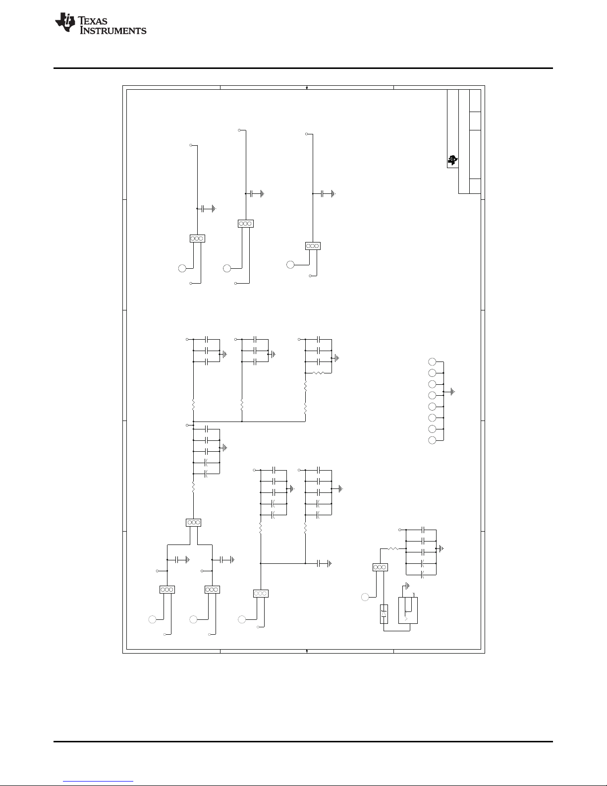
5
5
4
4
3
3
2
2
1
1
D D
C C
B B
A A
B -6519192
POWER DISTRIBUTION
18 28
REV PAGEDOCUMENT NUMBERSIZE
of
TEXAS INSTRUMENTS
PAGE TITLE
P4
GND
1
P16
1P0V_BJ
1
C181 68uf
+
C139 0.01uf
P9
GND
1
C125 1.0uf
C160 0.01uf
C137 1.0uf
C166
100uF
C189 0.01uf
C158 1.0uf
R176
0
R185
0
C182 10uf
+
P33
3P3V_BJ
1
P7
GND
1
C135 68uf
+
C141 68uf
+
C168 10uf
+
D9
BAT60A 10V, 3A
12
JMP149
3 Pin Berg Jumper
123
R178
0
C145 0.01uf
C255
100uF
R481
0
P6
GND
1
C136 10uf
+
R184 100
P20
1P8V_BJ
1
C127 0.01uf
C143 1.0uf
C286
100uF
C170 0.1uf
P8
GND
1
JMP85
3 Pin Berg Jumper
123
C142 10uf
+
JMP63
3 Pin Berg Jumper
123
C159 0.1uf
P15
1P5V_BJ
1
C133 0.01uf
C138 0.1uf
JMP89
3 Pin Berg Jumper
123
P2
GND
1
P23
5V_BJ
1
JMP59
3 Pin Berg Jumper
123
C131 1.0uf
R181
0
C169 1.0uf
R183 100
P29
2P5V_BJ
1
C122
100uF
C167 68uf
+
C188 0.1uf
C171 0.01uf
R177
0
P30
1P2V_BJ
1
JMP81
3 Pin Berg Jumper
123
P24
RAPC722
SILK = +5V
SLEEVE
1
SHUNT
2
TIP
3
C126 0.1uf
JMP70
3 Pin Berg Jumper
123
JMP58
3 Pin Berg Jumper
123
P5
GND
1
C153
100uF
C187 1.0uf
R179
0
C144 0.1uf
P3
GND
1
C132 0.1uf
C232
100uF
1P8V_REG
1P5V_REG
1P0V_REG
1P0V_BJ
1P8V_BJ
1P5V_BJ
5V_BARREL
5V_BJ
5V_DIODE
1P2V_BJ
2P5V_BJ
3p3V_BJ
VDDRA
1P0V
VREFT
1P5/8V
1P5V_REG
1P8V_REG
1P0V_REG
DVDD
1P8V
1P5V
VDDRB
5V
2P5V
1P2V
1P2V_REG
2P5V_REG
3P3V_REG
3P3V
VREFTA/B (VDDQx/2)
0.75V OR 0.9V
VDDRA
1.5V OR 1.8V
VDDQA/B, VDD01/2/3
1.5V OR 1.8V
AVDD, VDDT, VDDD
1.0V
DVDD
1.0V
NOTE: THE O OH M 1206 RESISTORS COULD BE REPLACED WITH A FERRITE BE ADS IF NEEDED.
VDDRB
1.5V OR 1.8
NOTE: PLACE GND BANANA JACKS 7 50 MIL
CENTER TO CENTER SPACING WITH A POWER
BANANA JACK LOCATED BETWEEN TWO POWER
JACKS AND OFFSET DIAGONALLY.
5V
2.5V
SUPPLY
1.2V
SUPPLY
www.ti.com
TLK6002EVM Schematics
SLLU132–October 2010 TLK6002 Dual-Channel, 0.47-Gbps to 6.25-Gbps, Multi-Rate Transceiver
Submit Documentation Feedback
Figure 35. Power Distribution, Sheet 18
Copyright © 2010, Texas Instruments Incorporated
Evaluation Module
43
Page 44

5
5
4
4
3
3
2
2
1
1
D D
C C
B B
A A
B -6519192
1P0V AND 1P2V SUPPLY LEDS
19 28
REV PAGEDOCUMENT NUMBERSIZE
of
TEXAS INSTRUMENTS
PAGE TITLE
R204
10.0K
R200 6.98K
R202
105K
JMP97
LED ENABLE
123
LM339AU25E
4 IN_P114 IN_N
10
4 OUT
13
-
+
R195
24.9K
C211
0.47uF
R196
105K
R194 49.9
R193 49.9
JMP94
LED ENABLE
123
R203
1.21k
LM339AU25D
3 IN_N83 IN_P
9
3 OUT
14
-
+
D11
HSMB-C170
21
U26
REF2940
VIN
1
VOUT
2
GND
3
R197
1.05K
LM339AU25A
VCC
3
GND
12
D10
HSMB-C170
21
JMP95
LED SELECT
123
R198
10.0K
JMP96
LED SELECT
123
R201
32.4k
LM339AU25C
2 IN_N42 IN_P
5
2 OUT
2
-
+
R199 11.0K
U27
ZXTD09N50DE6
C11E12C2
3
B2
4
E2
5
B1
6
LM339AU25B
1 IN_P71 IN_N
6
1 OUT
1
-
+
1P2V_VREF_HIGH
1P2V_VREF_LOW
1P2V_LED_IN
1P2V_LED_VF
1P0V_LED_VF
1P2V_LED_COL
1P0V_LED_COL
1P0V_LED_BASE
1P0V_VREF_HIGH
1P0V_VREF_LOW
1P0V_LED_IN 1P0V_LED_WINDOW_OUT
1P2V_LED_WINDOW_OUT
1P2V_LED_BASE
1P0V_LED_PLANE_OUT
1P2V_LED_PLANE_OUT
5V
5V
5V 5V
5V
1P2V
1P0V
5V
4P096V_REF1
1P0V
1P2V
NOTE: VOLTAG E WINDOW DETECTOR CIRCUITS MONITOR THE VOLTAGE ON THE PLANE
AND LIGHTS THE APPROPRIATE LED IF IT IS WITHIN THE A LLOWABLE DATASHEET
RANGE.
TLK6002EVM Schematics
www.ti.com
Figure 36. 1p0V and 1p2V Supply LEDs, Sheet 19
44
TLK6002 Dual-Channel, 0.47-Gbps to 6.25-Gbps, Multi-Rate Transceiver SLLU132–October 2010
Evaluation Module
Copyright © 2010, Texas Instruments Incorporated
Submit Documentation Feedback
Page 45
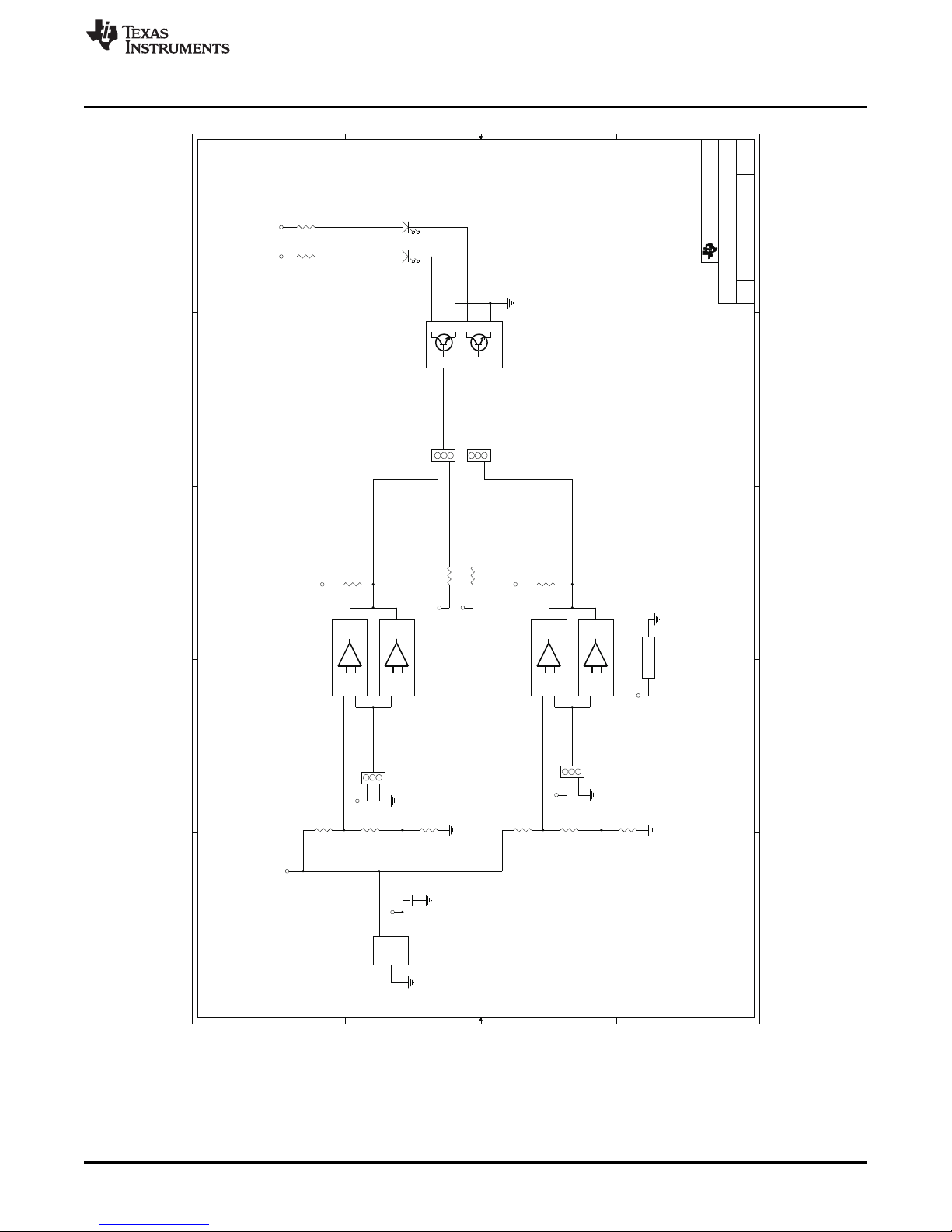
5
5
4
4
3
3
2
2
1
1
D D
C C
B B
A A
B -6519192
1P5V AND 1P8V SUPPLY LEDS
20 28
REV PAGEDOCUMENT NUMBERSIZE
of
TEXAS INSTRUMENTS
PAGE TITLE
R211 18.7K
D12
HSMB-C170
21
R213
13.0K
LM339AU28C
2 IN_N42 IN_P
5
2 OUT
2
-
+
U29
REF2940
VIN
1
VOUT
2
GND
3
JMP100
LED SELECT
123
R209
1.4K
JMP98
LED ENABLE
123
R210
9.76K
U30
ZXTD09N50DE6
C11E12C2
3
B2
4
E2
5
B1
6
R214
105K
R212 26.7K
R207
17.4K
LM339AU28E
4 IN_P114 IN_N
10
4 OUT
13
-
+
JMP101
LED ENABLE
123
R206 49.9D13
HSMB-C170
21
C212
0.47uF
R215
1.2K
LM339AU28B
1 IN_P71 IN_N
6
1 OUT
1
-
+
LM339AU28D
3 IN_N83 IN_P
9
3 OUT
14
-
+
LM339AU28A
VCC
3
GND
12
R208
105K
R205 49.9
JMP99
LED SELECT
123
R216
10.2K
1P5V_VREF_HIGH
1P5V_VREF_LOW
1P5V_LED_IN
1P5V_LED_VF
1P8V_LED_VF
1P5V_LED_COL
1P8V_LED_COL
1P8V_LED_BASE
1P8V_VREF_HIGH
1P8V_VREF_LOW
1P8V_LED_IN
1P5V_LED_BASE
1P8V_LED_WINDOW_OUT
1P5V_LED_WINDOW_OUT
1P5V_LED_PLANE_OUT
1P8V_LED_PLANE_OUT
5V
5V
5V 5V
5V
1P5V
1P8V
5V
4P096V_REF2
1P8V
1P5V
NOTE: VOLTAG E WINDOW DETECTOR CIRCUITS MONITOR THE VOLTAGE ON THE PLANE
AND LIGHTS THE APPROPRIATE LED IF IT IS WITHIN THE A LLOWABLE DATASHEET
RANGE.
www.ti.com
TLK6002EVM Schematics
SLLU132–October 2010 TLK6002 Dual-Channel, 0.47-Gbps to 6.25-Gbps, Multi-Rate Transceiver
Figure 37. 1p5V and 1p8V Supply LEDs, Sheet 20
Submit Documentation Feedback
Copyright © 2010, Texas Instruments Incorporated
45
Evaluation Module
Page 46
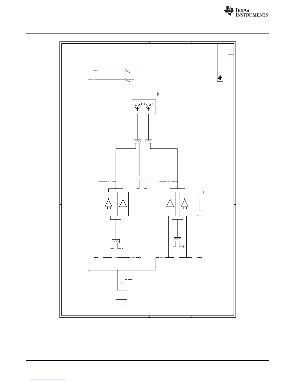
5
5
4
4
3
3
2
2
1
1
D D
C C
B B
A A
B -6519192
1P5V AND 1P8V SUPPLY LEDS
20 28
REV PAGEDOCUMENT NUMBERSIZE
of
TEXAS INSTRUMENTS
PAGE TITLE
R211 18.7K
D12
HSMB-C170
21
R213
13.0K
LM339AU28C
2 IN_N42 IN_P
5
2 OUT
2
-
+
U29
REF2940
VIN
1
VOUT
2
GND
3
JMP100
LED SELECT
123
R209
1.4K
JMP98
LED ENABLE
123
R210
9.76K
U30
ZXTD09N50DE6
C11E12C2
3
B2
4
E2
5
B1
6
R214
105K
R212 26.7K
R207
17.4K
LM339AU28E
4 IN_P114 IN_N
10
4 OUT
13
-
+
JMP101
LED ENABLE
123
R206 49.9D13
HSMB-C170
21
C212
0.47uF
R215
1.2K
LM339AU28B
1 IN_P71 IN_N
6
1 OUT
1
-
+
LM339AU28D
3 IN_N83 IN_P
9
3 OUT
14
-
+
LM339AU28A
VCC
3
GND
12
R208
105K
R205 49.9
JMP99
LED SELECT
123
R216
10.2K
1P5V_VREF_HIGH
1P5V_VREF_LOW
1P5V_LED_IN
1P5V_LED_VF
1P8V_LED_VF
1P5V_LED_COL
1P8V_LED_COL
1P8V_LED_BASE
1P8V_VREF_HIGH
1P8V_VREF_LOW
1P8V_LED_IN
1P5V_LED_BASE
1P8V_LED_WINDOW_OUT
1P5V_LED_WINDOW_OUT
1P5V_LED_PLANE_OUT
1P8V_LED_PLANE_OUT
5V
5V
5V 5V
5V
1P5V
1P8V
5V
4P096V_REF2
1P8V
1P5V
NOTE: VOLTAG E WINDOW DETECTOR CIRCUITS MONITOR THE VOLTAGE ON THE PLANE
AND LIGHTS THE APPROPRIATE LED IF IT IS WITHIN THE A LLOWABLE DATASHEET
RANGE.
TLK6002EVM Schematics
www.ti.com
46
TLK6002 Dual-Channel, 0.47-Gbps to 6.25-Gbps, Multi-Rate Transceiver SLLU132–October 2010
Figure 38. 2p5V, 3p3V, and 5V Supply LEDs, Sheet 21
Evaluation Module
Copyright © 2010, Texas Instruments Incorporated
Submit Documentation Feedback
Page 47
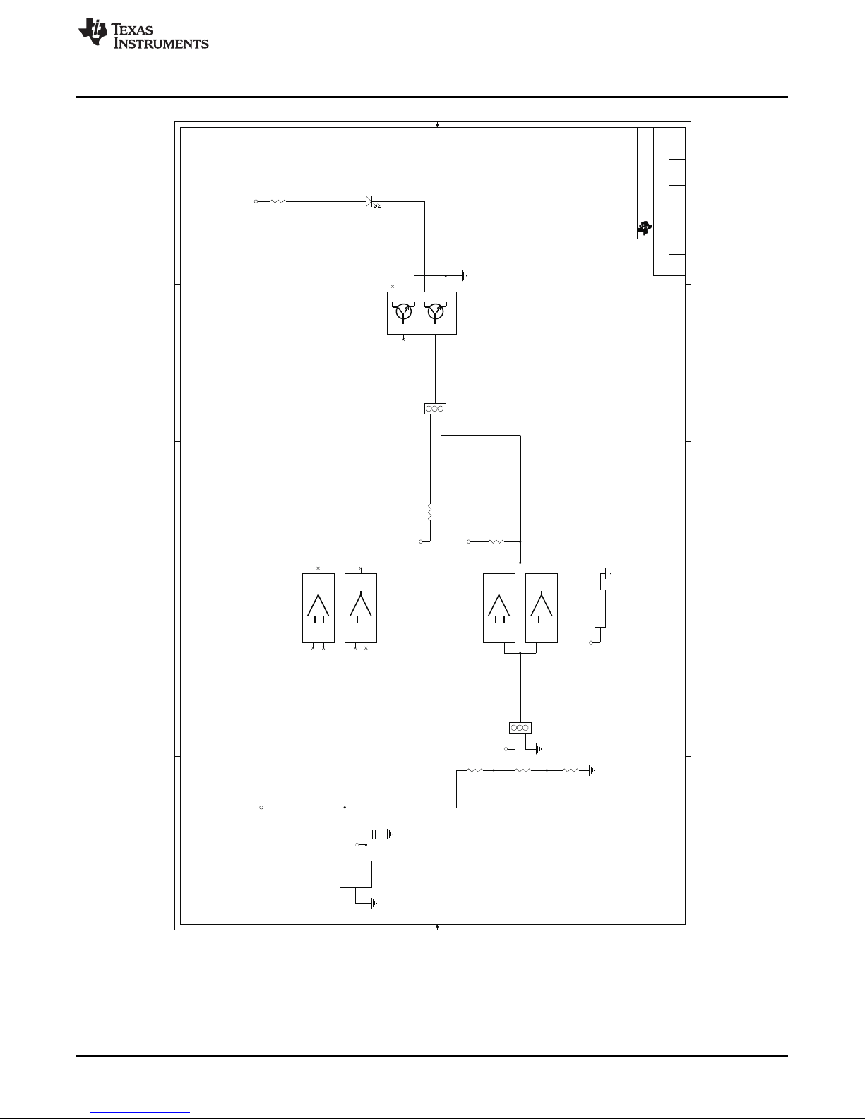
5
5
4
4
3
3
2
2
1
1
D D
C C
B B
A A
B -6519192
DVDD SUPPLY LEDS
22 28
REV PAGEDOCUMENT NUMBERSIZE
of
TEXAS INSTRUMENTS
PAGE TITLE
U39
ZXTD09N50DE6
C11E12C2
3
B2
4
E2
5
B1
6
R253
10.0K
LM339AU37C
2 IN_N42 IN_P
5
2 OUT
2
-
+
R252
1.21K
JMP113
LED ENABLE
123
U38
REF2940
VIN
1
VOUT
2
GND
3
LM339AU37B
1 IN_P71 IN_N
6
1 OUT
1
-
+
JMP112
LED SELECT
123
LM339AU37E
4 IN_P114 IN_N
10
4 OUT
13
-
+
R249 6.98K
R250
32.4K
R251
105K
LM339AU37D
3 IN_N83 IN_P
9
3 OUT
14
-
+
D20
HSMB-C170
21
C215
0.47uF
R243 49.9
LM339A
U37A
VCC
3
GND
12
DVDD_LED_VF
DVDD_LED_COL
DVDD_LED_BASE
DVDD_VREF_HIGH
DVDD_VREF_LOW
DVDD_LED_IN DVDD_LED_WINDOW_OUT
DVDD_LED_PLANE_OUT
5V
5V
5V
DVDD
5V
4P096V_REF5
DVDD
NOTE: VOLTAG E WINDOW DETECTOR CIRCUITS MONITOR THE VOLTAGE ON THE PLANE
AND LIGHTS THE APPROPRIATE LED IF IT IS WITHIN THE A LLOWABLE DATASHEET
RANGE.
www.ti.com
TLK6002EVM Schematics
Figure 39. DVDD Supply LEDs, Sheet 22
SLLU132–October 2010 TLK6002 Dual-Channel, 0.47-Gbps to 6.25-Gbps, Multi-Rate Transceiver
Submit Documentation Feedback
Copyright © 2010, Texas Instruments Incorporated
Evaluation Module
47
Page 48

5
5
4
4
3
3
2
2
1
1
D D
C C
B B
A A
B -6519192
1P5/8V SUPPLY LEDS
23 28
REV PAGEDOCUMENT NUMBERSIZE
of
TEXAS INSTRUMENTS
PAGE TITLE
R260 18.7K
LM339AU40E
4 IN_P114 IN_N
10
4 OUT
13
-
+
LM339AU40A
VCC
3
GND
12
R264
1.2K
JMP115
LED ENABLE
123
C216
0.47uF
JMP114
LED SELECT
123
R262
13.0K
R259
9.76K
R265
10.2K
R256
17.4K
LM339AU40C
2 IN_N42 IN_P
5
2 OUT
2
-
+
R254 49.9
R255 49.9
R258
1.4K
JMP116
LED SELECT
123
U41
REF2940
VIN
1
VOUT
2
GND
3
R263
105K
R257
105K
R261 26.7K
D22
HSMB-C170
21
LM339AU40B
1 IN_P71 IN_N
6
1 OUT
1
-
+
D21
HSMB-C170
21
U42
ZXTD09N50DE6
C11E12C2
3
B2
4
E2
5
B1
6
LM339AU40D
3 IN_N83 IN_P
9
3 OUT
14
-
+
1P5V_1P5/8V_VREF_HIGH
1P5V_1P5/8V_VREF_LOW
1P5V_1P5/8V_LED_VF
1P8V_1P5/8V_LED_VF
1P8V_1P5/8V_LED_COL
1P5V_1P5/8V_LED_COL
1P8V_1P5/8V_LED_BASE
1P8V_1P5/8V_VREF_LOW
1P8V_1P5/8V_VREF_HIGH
1P8V_1P5/8V_LED_WINDOW_OUT
1P5V_1P5/8V_LED_WINDOW_OUT
1P5/8V_LED_IN
1P5V_1P5/8V_LED_BASE
1P5V_1P5/8V_LED_PLANE_OUT
1P8V_1P5/8V_LED_PLANE_OUT
5V
5V
5V 5V
5V
1P5/8V
5V
4P096V_REF7
1P5/8V
NOTE: VOLTAG E WINDOW DETECTOR CIRCUITS MONITOR THE VOLTAGE ON THE PLANE
AND LIGHTS THE APPROPRIATE LED IF IT IS WITHIN THE A LLOWABLE DATASHEET
RANGE.
TLK6002EVM Schematics
www.ti.com
Figure 40. 1p5/8V Supply LEDs, Sheet 23
48
TLK6002 Dual-Channel, 0.47-Gbps to 6.25-Gbps, Multi-Rate Transceiver SLLU132–October 2010
Evaluation Module
Copyright © 2010, Texas Instruments Incorporated
Submit Documentation Feedback
Page 49

5
5
4
4
3
3
2
2
1
1
D D
C C
B B
A A
B -6519192
VDDRA SUPPLY LEDS
24 28
REV PAGEDOCUMENT NUMBERSIZE
of
TEXAS INSTRUMENTS
PAGE TITLE
D31
HSMB-C170
21
C221
0.47uF
R314 49.9
LM339AU55D
3 IN_N83 IN_P
9
3 OUT
14
-
+
R321 26.7K
R316
17.4K
LM339AU55E
4 IN_P114 IN_N
10
4 OUT
13
-
+
LM339AU55C
2 IN_N42 IN_P
5
2 OUT
2
-
+
R317
105K
U56
REF2940
VIN
1
VOUT
2
GND
3
U57
ZXTD09N50DE6
C11E12C2
3
B2
4
E2
5
B1
6
LM339AU55B
1 IN_P71 IN_N
6
1 OUT
1
-
+
R324
1.2K
R322
13.0K
JMP129
LED SELECT
123
R320 18.7K
JMP130
LED ENABLE
123
R319
9.76K
LM339AU55A
VCC
3
GND
12
R323
105K
R318
1.4K
R325
10.2K
R315 49.9D32
HSMB-C170
21
JMP131
LED SELECT
123
1P5V_VDDRA_VREF_HIGH
1P5V_VDDRA_VREF_LOW
1P5V_VDDRA_LED_VF
1P5V_VDDRA_LED_BASE
1P8V_VDDRA_LED_VF
1P8V_VDDRA_LED_COL
1P5V_VDDRA_LED_COL
1P8V_VDDRA_LED_BASE
1P8V_VDDRA_VREF_LOW
1P8V_VDDRA_VREF_HIGH
1P8V_VDDRA_LED_WINDOW_OUT
1P5V_VDDRA_LED_WINDOW_OUT
VDDRA_LED_IN
1P5V_VDDRA_LED_PLANE_OUT
1P8V_VDDRA_LED_PLANE_OUT
5V
5V
5V 5V
5V
VDDRA
5V
4P096V_REF12
VDDRA
NOTE: VOLTAG E WINDOW DETECTOR CIRCUITS MONITOR THE VOLTAGE ON THE PLANE
AND LIGHTS THE APPROPRIATE LED IF IT IS WITHIN THE A LLOWABLE DATASHEET
RANGE.
www.ti.com
TLK6002EVM Schematics
Figure 41. VDDRA Supply LEDs, Sheet 24
SLLU132–October 2010 TLK6002 Dual-Channel, 0.47-Gbps to 6.25-Gbps, Multi-Rate Transceiver
Submit Documentation Feedback
Copyright © 2010, Texas Instruments Incorporated
Evaluation Module
49
Page 50

5
5
4
4
3
3
2
2
1
1
D D
C C
B B
A A
B -6519192
VDDRB SUPPLY LEDS
25 28
REV PAGEDOCUMENT NUMBERSIZE
of
TEXAS INSTRUMENTS
PAGE TITLE
R330
1.4K
LM339AU58D
3 IN_N83 IN_P
9
3 OUT
14
-
+
LM339AU58A
VCC
3
GND
12
LM339AU58C
2 IN_N42 IN_P
5
2 OUT
2
-
+
D34
HSMB-C170
21
U59
REF2940
VIN
1
VOUT
2
GND
3
R328
17.4K
R337
10.2K
R334
13.0K
R331
9.76K
R326 49.9
R333 26.7K
R332 18.7K
R335
105K
R329
105K
U60
ZXTD09N50DE6
C11E12C2
3
B2
4
E2
5
B1
6
JMP134
LED SELECT
123
LM339AU58E
4 IN_P114 IN_N
10
4 OUT
13
-
+
R327 49.9
JMP132
LED SELECT
123
D33
HSMB-C170
21
LM339AU58B
1 IN_P71 IN_N
6
1 OUT
1
-
+
R336
1.2K
C222
0.47uF
JMP133
LED ENABLE
123
1P5V_VDDRB_VREF_HIGH
1P5V_VDDRB_VREF_LOW
1P5V_VDDRB_LED_VF
1P5V_VDDRB_LED_BASE
1P8V_VDDRB_LED_VF
1P8V_VDDRB_LED_COL
1P5V_VDDRB_LED_COL
1P8V_VDDRB_LED_BASE
1P8V_VDDRB_VREF_LOW
1P8V_VDDRB_VREF_HIGH
1P8V_VDDRB_LED_WINDOW_OUT
1P5V_VDDRB_LED_WINDOW_OUT
VDDRB_LED_IN
1P5V_VDDRB_LED_PLANE_OUT
1P8V_VDDRB_LED_PLANE_OUT
5V
5V
5V 5V
5V
VDDRB
5V
4P096V_REF13
VDDRB
NOTE: VOLTAG E WINDOW DETECTOR CIRCUITS MONITOR THE VOLTAGE ON THE PLANE
AND LIGHTS THE APPROPRIATE LED IF IT IS WITHIN THE A LLOWABLE DATASHEET
RANGE.
TLK6002EVM Schematics
www.ti.com
Figure 42. VDDRB Supply LEDs, Sheet 25
50
TLK6002 Dual-Channel, 0.47-Gbps to 6.25-Gbps, Multi-Rate Transceiver SLLU132–October 2010
Evaluation Module
Copyright © 2010, Texas Instruments Incorporated
Submit Documentation Feedback
Page 51

5
5
4
4
3
3
2
2
1
1
D D
C C
B B
A A
B -6519192
VREFT SUPPLY LEDS
26 28
REV PAGEDOCUMENT NUMBERSIZE
of
TEXAS INSTRUMENTS
PAGE TITLE
R354
1.4K
JMP140
LED SELECT
123
LM339AU64E
4 IN_P114 IN_N
10
4 OUT
13
-
+
U66
ZXTD09N50DE6
C11E12C2
3
B2
4
E2
5
B1
6
LM339AU64A
VCC
3
GND
12
U65
REF2940
VIN
1
VOUT
2
GND
3
C224
0.47uF
R359
105K
R353
105K
R350 49.9
D38
HSMB-C170
21
R360
1.15K
R355
10.0K
LM339AU64B
1 IN_P71 IN_N
6
1 OUT
1
-
+
R351 49.9
R358
36.0K
LM339AU64D
3 IN_N83 IN_P
9
3 OUT
14
-
+
R361
9.76K
R356 1.0K
R357 3.9K
JMP139
LED ENABLE
123
LM339AU64C
2 IN_N42 IN_P
5
2 OUT
2
-
+
R352
47.0K
JMP138
LED SELECT
123
D37
HSMB-C170
21
0P75V_VREFT_VREF_HIGH
0P75V_VREFT_VREF_LOW
0P75V_VREFT_LED_VF
0P75V_VREFT_LED_BASE
0P9V_VREFT_LED_VF
0P9V_VREFT_LED_COL
0P75V_VREFT_LED_COL
0P9V_VREFT_LED_BASE
0P9V_VREFT_VREF_LOW
0P9V_VREFT_VREF_HIGH
0P9V_VREFT_LED_WINDOW_OUT
0P75V_VREFT_LED_WINDOW_OUT
VREFT_LED_IN
0P75V_VREFT_LED_PLANE_OUT
0P9V_VREFT_LED_PLANE_OUT
5V
5V
5V 5V
5V
VREFT
5V
4P096V_REF15
VREFT
NOTE: VOLTAG E WINDOW DETECTOR CIRCUITS MONITOR THE VOLTAGE ON THE PLANE
AND LIGHTS THE APPROPRIATE LED IF IT IS WITHIN THE A LLOWABLE DATASHEET
RANGE.
www.ti.com
TLK6002EVM Schematics
Figure 43. VREFT Supply LEDs, Sheet 26
SLLU132–October 2010 TLK6002 Dual-Channel, 0.47-Gbps to 6.25-Gbps, Multi-Rate Transceiver
Submit Documentation Feedback
Copyright © 2010, Texas Instruments Incorporated
Evaluation Module
51
Page 52

5
5
4
4
3
3
2
2
1
1
D D
C C
B B
A A
B -6519192
NO CONNECT PINS
27 28
REV PAGEDOCUMENT NUMBERSIZE
of
TEXAS INSTRUMENTS
PAGE TITLE
TLK60X2
U1-27
NC33N9NC25
F13
TLK60X2
U1-31
NC56H9NC57H8NC58
H11
NC59
H10
NC60
E13
NC61
D13
NC62
D9
TLK60X2
U1-28
NC26E6NC27F6NC28G6NC29H6NC30B7NC31E7NC32C8NC34J8NC35B9NC36C9NC37J9NC38
J10
NC39
J11
NC40
J12
NC41
B11
NC42
C11
NC43
E12
NC44
F12
NC45
G13
TLK60X2
U1-29
NC46D7NC47C7NC48
C12
NC49
B12
TLK60X2
U1-26
NC0A7NC1A9NC2
A11
NC3
A12
NC4
C10
NC5
C13
NC6H7NC7D8NC8
D10
NC9
D11
NC10
D12
NC11E8NC12E9NC13
E10
NC14
E11
NC15F8NC16F9NC17
F10
NC18
F11
NC19G8NC20G9NC21
G10
NC22
G11
NC23
G12
NC24
H12
TLK60X2
U1-30
NC50G7NC51F7NC52A8NC53B8NC54
A10
NC55
B10
TLK60X2
U1-32
NC63
A13
NC64
B14
NC65
A14
NC66
B13
NC67K7NC68
J13
NC69
C14
R555
0
PIN_N9
DVDD
TLK6002EVM Schematics
www.ti.com
52
TLK6002 Dual-Channel, 0.47-Gbps to 6.25-Gbps, Multi-Rate Transceiver SLLU132–October 2010
Evaluation Module
Figure 44. No Connect Pins, Sheet 27
Copyright © 2010, Texas Instruments Incorporated
Submit Documentation Feedback
Page 53
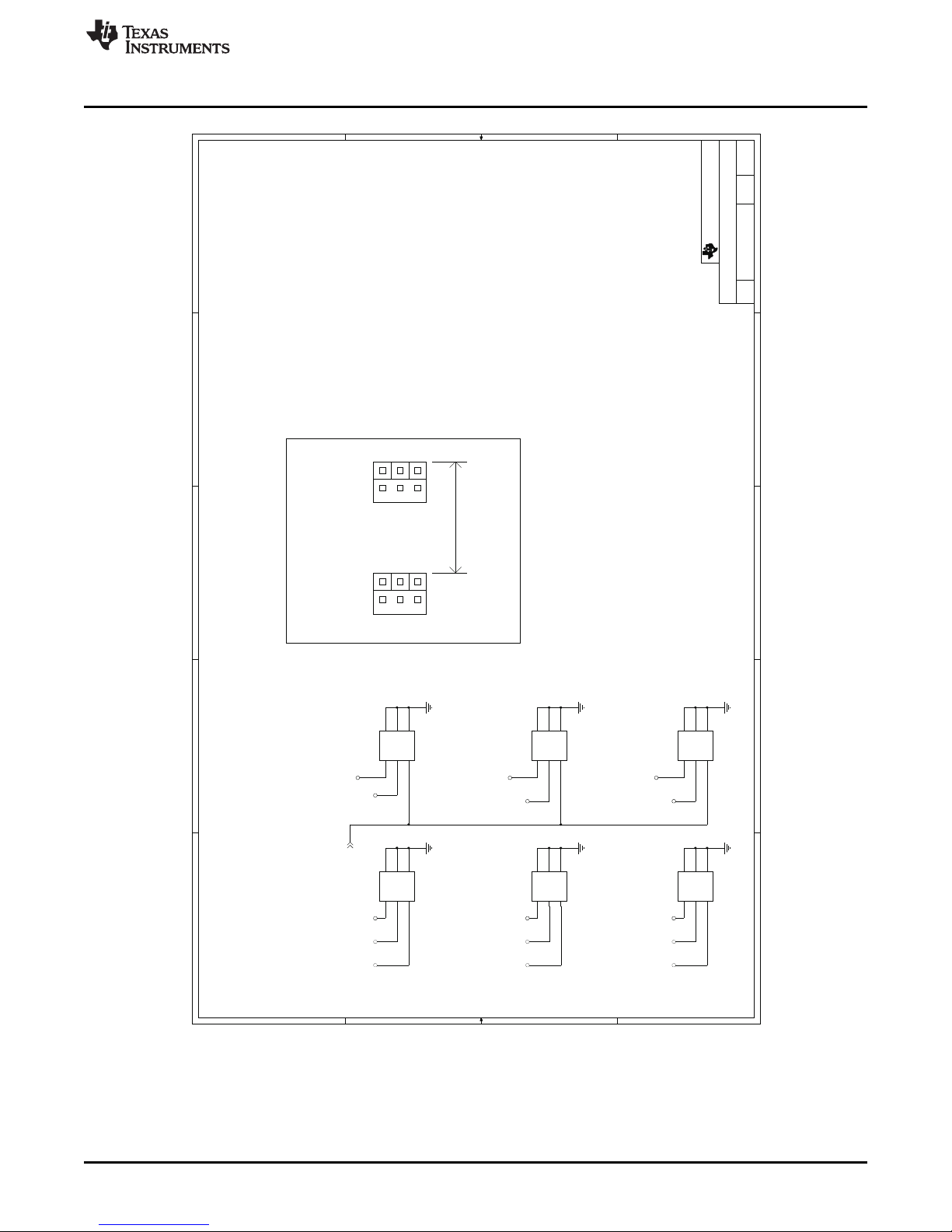
5
5
4
4
3
3
2
2
1
1
D D
C C
B B
A A
B -6519192
PERIPHERAL PORTS
28 28
REV PAGEDOCUMENT NUMBERSIZE
of
TEXAS INSTRUMENTS
PAGE TITLE
J29B
LST-103-07-S-D
P4
7
S4
8
P5
9
S5
10
P6
11
S6
12
J28A
LST-103-07-S-D
P11P2
3
S12S2
4
P3
5
S3
6
J27A
LST-103-07-S-D
P11P2
3
S12S2
4
P3
5
S3
6
J27B
LST-103-07-S-D
P4
7
S4
8
P5
9
S5
10
P6
11
S6
12
J29A
LST-103-07-S-D
P11P2
3
S12S2
4
P3
5
S3
6
J28B
LST-103-07-S-D
P4
7
S4
8
P5
9
S5
10
P6
11
S6
12
RST_N
PERIPH3_1P5_1P8
PERIPH2_1P5_1P8
PERIPH1_1P5_1P8
5V
5V
2P5V
2P5V
1P2V
1P2V
3P3V
3P3V
1P2V5V2P5V
3P3V
1P5/8V
1P5/8V
1P5/8V
RST_N3,38
P1
P4
S1
S4
1.5 IN
SPACING
PERIPHERAL PORT LAYOUT
NOTE: THREE PERIPHERAL PORTS ARE INCLUDED ON T HIS BOARD TO ALLOW FOR OSCILLATOR/CLOCK CIRCUITS, OPTICAL MODULES,
AND ANY OTHER POSSIBLE MODULE THAT WOULD ALLOW FOR MORE AUTONOMOUS OPERATION AND TESTING OF THE TLK6002 DEVICE.
THEY SIMPLY PROVIDE POWER AND THE GLOBAL RESET (RST_N) SIGNAL THROUGH TWO TERMINAL/SOCKET COMBINATION CON NECTORS.
THESE CONNECTORS WERE CHOSENAND LAID OUT SUCH THAT THE PERIPHERAL MODULE WILL NOT BE ABLE TO BE INSTALL ED
INCORRECTLY. THERE WILL ALSO BE A NOTICABLE "CLIC K" WHEN THE MODULE IS PROPERLY INSERTED.
PINS
PINS
SOCKETS
SOCKETS
P2
P5
S2
S5
P3
P6
S3
S6
www.ti.com
TLK6002EVM Schematics
SLLU132–October 2010 TLK6002 Dual-Channel, 0.47-Gbps to 6.25-Gbps, Multi-Rate Transceiver
Submit Documentation Feedback
Figure 45. Peripheral Ports, Sheet 28
Copyright © 2010, Texas Instruments Incorporated
Evaluation Module
53
Page 54

TLK6002EVM Bill of Materials
www.ti.com
15 TLK6002EVM Bill of Materials
Table 1. Bill of Materials
Item Qty Reference Value Part Part_Number Manufacturer
1 3 C51, C322, C323 0.1mF 0201 CAP C0201X5R6R3-104KNE Venkel
2 15 C52, C64, C65, C66, C67, C68, C69, 10000pF 0201 CAP GRM033R71A103KA01D Murata Electronics
C70,C71, C72, C73, C74, C75, C76, C77
3 4 C11, C27, C38, C58 0.01mF 0402 CAP C0402X7R500-103KNE Venkel
4 12 C9, C10, C25, C37, C41, C42, C43, 0.1mF 0402 CAP C0402X7R160-104KNE Venkel
C57,C315, C316, C320, C321
5 7 C7, C8, C23, C24, C36, C50, C56 0.22mF 0402 CAP EMK105BJ224KV-F Taiyo Yuden
6 7 C5, C6, C21, C22, C35, C49, C55 0.47mF 0402 CAP C0402X5R6R3-474KNE Venkel
7 7 C3, C4, C19, C20, C34, C48, C319 1.0mF 0402 CAP GRM155R61A105KE15D Murata Electronics
8 3 C13, C29, C39 1000pF 0402 CAP C0402COG500-102JNE Venkel
9 2 C15, C31 100pF 0402 CAP C0402COG500-101JNE Venkel
10 6 C1, C2, C17, C18, C33, C47 2.2mF 0402 CAP GRM155R60J225ME15D Murata Electronics
11 1 C59 0.1mF 0603CAP 06033C104JAT2A Avx Corporation
12 9 C121, C211, C212, C213, C215, C216, 0.47mF 0603 CAP C0603X7R160-474KNE Venkel
C221, C222, C224
13 7 C88, C95, C102, C109, C116, C236, C258 1.0mF 0603 CAP C1608X7R1C105K Tdk Corporation
14 6 C92, C99, C106, C113, C120, C240 1000pF 0603 CAP C0603COG500-102JNE Venkel
15 4 C84, C85, C256, C318 2.2mF 0603 CAP GRM188R71A225KE15D Murata Electronics
16 7 C87, C94, C101, C108, C115, C235, C317 4.7mF 0603 CAP C0603X5R6R3-475KNE Venkel
17 7 C127, C133, C139, C145, C160, C171, 0.01mF 0805 CAP GRM21BR72A103KA01L Murata Electronics
C189
18 7 C126, C132, C138, C144, C159, C170, 0.1mF 1206 CAP C1206C104J5RACTU Kemet
C188
19 13 C91, C98, C105, C112, C119, C125, C131, 1.0mF 1206 CAP C1206X7R500-105KNE Murata Electronics
C137, C143, C158, C169, C187, C239
20 12 C86, C93, C100, C107, C114, C122, C153, 100mF 1812CAP GRM43SR60J107ME20L Murata Electronics
C166, C232, C234, C255, C286
21 10 C90, C97, C104, C111, C118, C136, C142, 10mF 7343-43 (EIA) B45197A7106K509 Kemet
C168, C182, C238
22 10 C89, C96, C103, C110, C117, C135, C141, 68mF - LESR 7361-38 (EIA) B45197A4686K409 Kemet
C167, C181, C237
23 11 R16, R139, R167, R169, R171, R173, 0.0 (Zero Ω) 0402 RES ERJ-2GE0R00X Panasonic - Ecg
R496, R516, R547, R549, R555
24 1 R145 1.82K 0402 RES ERJ-2RKF1821X Panasonic - Ecg
25 4 R142, R148, R155, R162 10.0K 0402 RES RG1005P-103-B-T5 Susumu Co Ltd
54
TLK6002 Dual-Channel, 0.47-Gbps to 6.25-Gbps, Multi-Rate Transceiver SLLU132– October 2010
Evaluation Module
Submit Documentation Feedback
Copyright © 2010, Texas Instruments Incorporated
Page 55

www.ti.com
TLK6002EVM Bill of Materials
Table 1. Bill of Materials (continued)
Item Qty Reference Value Part Part_Number Manufacturer
26 1 R151 10.5K 0402 RES RG1005P-1052-B-T5 Susumu Co Ltd
27 2 R508, R526 100K 0402 RES RC0402FR-07100KL Yageo America
28 4 R168, R170, R172, R175 105K 0402 RES ERJ-2RKF1053X Panasonic - Ecg
29 3 R163, R164, R166 130 0402 RES RG1005P-131-B-T5 Susumu Co Ltd
30 1 R153 2.87K 0402 RES RR0510P-2871-D Susumu Co Ltd
31 6 R11, R12, R445, R446, R556, R558 20K 0402 RES ERJ-2RKF2002X Panasonic - Ecg
32 1 R143 3.09K 0402 RES ERJ-2RKF3091X Panasonic - Ecg
33 1 R158 30.9K 0402 RES ERJ-2RKF3092X Panasonic - Ecg
34 21 R491, R492, R493, R494, R495, R497, 4.99K 0402 RES CR0402-16W-4991FT Venkel
R498, R499, R505, R506, R509, R510,
R511, R512, R513, R514, R515, R517,
R523, R524, R529
35 4 R38, R39, R520, R522 45.3K 0402 RES ERJ-2RKF4532X Panasonic - Ecg
36 3 R165, R507, R525 49.9 0402 RES RG1005P-49R9-B-T5 Susumu Co Ltd
37 4 R18, R19, R20, R21 49.9 0402 RES RR0510R-49R9-D Susumu Co Ltd
38 1 R161 6.65K 0402 RES ERJ-2RKF6651X Panasonic - Ecg
39 1 R141 910 0402 RES RG1005P-911-B-T5 Susumu Co Ltd
40 12 R56, R57, R73, R74, R90, R91, R107, 0.0 (Zero Ω) 0603 RES ERJ-3GEY0R00V Panasonic - Ecg
R108, R124, R125, R364, R365
41 17 R356, R423, R424, R425, R435, R436, 1.00K 0603 RES RR0816P-102-B-T5 Susumu Co Ltd
R437, R442, R447, R448, R449, R450,
R455, R456, R471, R487, R488
42 1 R228 1.02K 0603 RES TNPW06031K02BEEA Vishay/Dale
43 1 R197 1.05K 0603 RES RR0816P-1051-B-T5-03H Susumu Co Ltd
44 1 R221 1.10K 0603 RES RG1608P-112-B-T5 Susumu Co Ltd
45 1 R123 1.13K 0603 RES RR0816P-1131-D-06H Susumu Co Ltd
46 1 R360 1.15K 0603 RES RG1608P-1151-B-T5 Susumu Co Ltd
47 5 R215, R264, R324, R336, R371 1.20K 0603 RES RG1608P-122-B-T5 Susumu Co Ltd
48 2 R203, R252 1.21K 0603 RES RG1608P-1211-B-T5 Susumu Co Ltd
49 1 R150 1.27K 0603 RES RR0816P-1271-D-11H Susumu Co Ltd
50 5 R209, R258, R318, R330, R354 1.40K 0603 RES RG1608P-1401-B-T5 Susumu Co Ltd
51 4 R42, R43, R44, R45 1.50K 0603 RES RG1608P-152-B-T5 Susumu Co Ltd
52 1 R63 1.69K 0603 RES RG1608P-1691-B-T5 SusumuCo Ltd
53 1 R225 1.96K 0603 RES RN731JTTD1961B25 Koa Speer
54 7 R146, R156, R198, R204, R222, R253, 10.0K 0603 RES ERA-3AEB103V Panasonic - Ecg
R355
55
SLLU132– October 2010 TLK6002 Dual-Channel, 0.47-Gbps to 6.25-Gbps, Multi-Rate Transceiver
Evaluation Module
Submit Documentation Feedback
Copyright © 2010, Texas Instruments Incorporated
Page 56

TLK6002EVM Bill of Materials
www.ti.com
Table 1. Bill of Materials (continued)
Item Qty Reference Value Part Part_Number Manufacturer
55 4 R216, R265, R325, R337 10.2K 0603 RES RG1608P-1022-B-T5 Susumu Co Ltd
56 3 R60, R65, R154 10.5K 0603 RES RG1608P-1052-B-T5 Susumu Co Ltd
57 1 R149 100 0603 RES RG1608P-101-B-T5 Susumu Co Ltd
58 1 R4 100K 0603 RES TNPW06031003BT9 Vishay/Dale
59 15 R196, R202, R208, R214, R220, R227, 105K 0603 RES RR0816P-1053-B-T5-03D Susumu Co Ltd
R251, R257, R263, R317, R323, R329,
R335, R353, R359
60 1 R199 11K 0603RES RG1608P-113-B-T5 Susumu Co Ltd
61 1 R136 127 0603 RES ERJ-3EKF1270V Panasonic - Ecg
62 4 R213, R262, R322, R334 13.0K 0603 RES RG1608P-133-B-T5 Susumu Co Ltd
63 9 R2, R5, R24, R25, R68, R519, R521, R557, 130 0603 RES RG1608P-131-B-T5 Susumu Co Ltd
R559
64 1 R85 133 0603 RES RG1608P-1330-B-T5 Susumu Co Ltd
65 2 R93, R97 14.0K 0603 RES TNPW060314K0BEEA Vishay/Dale
66 1 R160 15.0K 0603 RES RG1608P-153-B-T5 Susumu Co Ltd
67 2 R76, R82 16.2K 0603 RES RR0816P-1622-D-21C Susumu Co Ltd
68 2 R110, R114 16.5K 0603 RES RG1608P-1652-B-T5 Susumu Co Ltd
69 2 R369, R372 16.9K 0603 RES TNPW060316K9BEEA Vishay/Dale
70 2 R128, R138 169 0603 RES TNPW0603169RBEEN Vishay/Dale
71 4 R207, R256, R316, R328 17.4K 0603 RES RR0816P-1742-B-T5-24C Susumu Co Ltd
72 2 R130, R132 18.0K 0603 RES RG1608P-183-B-T5 Susumu Co Ltd
73 4 R211, R260, R320, R332 18.7K 0603 RES RG1608P-1872-B-T5 Susumu Co Ltd
74 1 R106 2.49K 0603 RES RG1608P-2491-B-T5 Susumu Co Ltd
75 2 R368, R378 200 0603 RES RG1608P-201-B-T5 Susumu Co Ltd
76 2 R62, R64 21.5K 0603 RES RN731JTTD2152B25 Koa Speer
77 1 R376 23.2 0603 RES ERJ-3EKF23R2V Panasonic - Ecg
78 1 R195 24.9K 0603 RES RG1608P-2492-B-T5 Susumu Co Ltd
79 1 R119 243 0603 RES 288-0603-243-RC Xicon
80 4 R212, R261, R321, R333 26.7K 0603 RES RR0816P-2672-B-T5-42C Susumu Co Ltd
81 2 R96, R98 28.0K 0603 RES RNCF 16 T9 28K .1% I Stackpole Electronics Inc
82 2 R77, R87 280 0603 RES TNPW0603280RBEEA Vishay/Dale
83 2 R94, R104 294 0603 RES MCR03EZPFX2940 Rohm
84 1 R95 3.09K 0603 RES RN731JTTD3091B25 Koa Speer
85 1 R147 3.30K 0603 RES RG1608P-332-B-T5 Susumu Co Ltd
86 3 R55, R89, R363 3.57K 0603 RES RG1608P-3571-B-T5 Susumu Co Ltd
56
TLK6002 Dual-Channel, 0.47-Gbps to 6.25-Gbps, Multi-Rate Transceiver SLLU132– October 2010
Evaluation Module
Submit Documentation Feedback
Copyright © 2010, Texas Instruments Incorporated
Page 57

www.ti.com
TLK6002EVM Bill of Materials
Table 1. Bill of Materials (continued)
Item Qty Reference Value Part Part_Number Manufacturer
87 1 R357 3.90K 0603 RES RG1608P-392-B-T5 Susumu Co Ltd
88 6 R78, R81, R113, R115, R201, R250 32.4K 0603 RES RG1608P-3242-B-T5 Susumu Co Ltd
89 2 R61, R69 340 0603 RES 288-0603-340-RC Xicon
90 1 R358 36.0K 0603 RES RR0816P-363-B-T5 Susumu Co Ltd
91 2 R370, R377 392 0603 RES TNPW0603392RBEEN Vishay/Dale
92 1 R72 4.12K 0603 RES RG1608P-4121-B-T5 Susumu Co Ltd
93 37 R1, R6, R7, R8, R22, R23, R26, R28, R29, 4.99K 0603RES RG1608P-4991-B-T5 Susumu Co Ltd
R30, R31, R32, R33, R34, R35, R37, R40,
R41, R48, R49, R50, R51, R52, R54, R71,
R88, R105, R122, R140, R144, R152,
R159, R362, R422, R438, R467, R527
94 1 R223 41.2K 0603 RES RG1608P-4122-B-T5 Susumu Co Ltd
95 2 R59, R70 453 0603 RES RG1608P-4530-B-T5 Susumu Co Ltd
96 1 R352 47.0K 0603 RES RG1608P-473-B-T5 Susumu Co Ltd
97 19 R3, R193, R194, R205, R206, R217, R218, 49.9 0603 RES RG1608P-49R9-B-T1 Susumu Co Ltd
R226, R243, R254, R255, R314, R315,
R326, R327, R350, R351, R443, R444
98 1 R80 5.36K 0603 RES TNPW06035K36BEEA Vishay/Dale
99 1 R157 5.60K 0603 RES RG1608P-562-B-T5 Susumu Co Ltd
100 1 R112 5.62K 0603 RES RG1608P-5621-B-T5 Susumu Co Ltd
101 1 R129 5.90K 0603 RES RG1608P-5901-B-T5 Susumu Co Ltd
102 2 R79, R86 576 0603 RES ERJ-3EKF5760V Panasonic- Ecg
103 1 R219 6.19K 0603 RES RR0816P-6191-B-T5-77H Susumu Co Ltd
104 2 R200, R249 6.98K 0603 RES CR0603-10W-6981FT Venkel
105 1 R224 60.4K 0603 RES ERJ-3EKF6042V Panasonic - Ecg
106 2 R99, R103 619 0603 RES RR0816P-6190-D-77A Susumu Co Ltd
107 2 R111, R121 66.5 0603 RES MCR03EZPFX66R5 Rohm
108 2 R116, R120 665 0603 RES TNPW0603665RBEEN Vishay/Dale
109 2 R367, R373 8.45K 0603 RES RG1608P-8451-B-T5 Susumu Co Ltd
110 2 R127, R131 8.87K 0603 RES TNPW06038K87BEEN Vishay/Dale
111 1 R102 82.5 0603 RES RR0816Q-82R5-D-89R Susumu Co Ltd
112 2 R133, R137 86.6 0603 RES ERJ-3EKF86R6V Panasonic - Ecg
113 6 R210, R229, R259, R319, R331, R361 9.76K 0603 RES RG1608P-9761-B-T5 Susumu Co Ltd
114 2 R183, R184 100 0805 RES RG2012P-101-B-T5 Susumu Co Ltd
115 7 R176, R177, R178, R179, R181, R185, 0.0 (Zero Ω ) 1210 RES RK73Z2ETTE Koa Speer
R481
57
SLLU132– October 2010 TLK6002 Dual-Channel, 0.47-Gbps to 6.25-Gbps, Multi-Rate Transceiver
Evaluation Module
Submit Documentation Feedback
Copyright © 2010, Texas Instruments Incorporated
Page 58

TLK6002EVM Bill of Materials
www.ti.com
Table 1. Bill of Materials (continued)
Item Qty Reference Value Part Part_Number Manufacturer
116 1 D9 Zener Diode SOD-323 BAT 60A E6327 Infineon Technologies
117 6 Q1, Q2, Q3, Q4, Q5, Q6 NFET SOT-23 FDV301N Fairchild Semiconductor
118 15 U3, U4, U5, U22, U23, U27, U30, U33, U39, Dual NPN SOT-23-6 ZXTD09N50DE6TA Zetex Inc
U42, U57, U60, U66, U88, U92
119 1 U24 3-Input NAND 14-SOIC CD4023BME4 Texas Instruments
120 10 U16, U20, U25, U28, U31, U37, U40, U55, Differential 14-SOIC LM339AD TexasInstruments
U58, U64 Comparator
121 2 U18, U21 2-Input NAND 14-SOIC (3.9mm Width) CD4011BM Texas Instruments
122 2 U17, U19 3-Input NOR 14-SOIC (3.9mm Width) CD4025BM96 Texas Instruments
123 6 U7, U9, U11, U12, U14, U67 Quadruple FET 14-SOIC (3.9mm Width) SN74CBT3125D Texas Instruments
Bus Switch
124 2 U85, U86 J/K Flip-Flop 14-TSSOP SN74LVC112APWR Texas Instruments
125 4 U82, U83, U84, U91 Bi-Directional Level 20-QFN TXS0108ERGYR Texas Instruments
Shifter
126 6 U6, U8, U10, U13, U69, U70 Adjustable LDO 7-DD TPS74201KTWT Texas Instruments
127 9 U15, U26, U29, U32, U38, U41, U56, U59, Precision Voltage SOT-23 REF2940AIDBZT Texas Instruments
U65 Reference
128 3 U2, U87, U89 Voltage Supervisor SOT-23-5 TPS3125J18DBVR Texas Instruments
with Manual Reset
129 1 U90 Bi-Directional Level SOT-23-6 SN74AVCH1T45DCKR Texas Instruments
Shifter
130 1 U1 6.25Gbps SerDes 324 PBGA TLK6002 Texas Instruments
131 21 D7, D10, D11, D12, D13, D14, D15, D16, LED - Blue C170 HSMB-C170 Avago Technologies Us Inc
D20, D21, D22, D31, D32, D33, D34, D37, Diffused
D38, D41, D42, D51, D52
132 4 D2, D6, D4, D50 LED - Green C170 HSMG-C170 AvagoTechnologies Us Inc
Diffused
133 4 D1, D5, D3, D49 LED - Red C170 SML-LXT0805IW-TR Lumex Opto/Components Inc
Diffused
134 1 D8 LED - Yellow C170 HSMY-C170 Avago Technologies Us Inc
Diffused
135 3 SW1, SW3, SW4 Push Button 6mm EVQ-PBE05R Panasonic - Ecg
136 6 J27, J28, J29 Connector 0.1x0.1” LST-103-07-S-D Samtec
137 1 JMP30 20 Pin - Shrouded 0.1" SP 5103308-5 Tyco Electronics/Amp
138 19 JMP1, JMP3, JMP4, JMP6, JMP7, 1 X 2 0.1" HTSW-150-08-G-S Samtec
JMP8,JMP15, JMP31, JMP16, JMP24,
JMP25, JMP28, JMP21, JMP46, JMP48,
JMP50, JMP52, JMP54, JMP147
58
TLK6002 Dual-Channel, 0.47-Gbps to 6.25-Gbps, Multi-Rate Transceiver SLLU132– October 2010
Evaluation Module
Submit Documentation Feedback
Copyright © 2010, Texas Instruments Incorporated
Page 59

www.ti.com
TLK6002EVM Bill of Materials
Table 1. Bill of Materials (continued)
Item Qty Reference Value Part Part_Number Manufacturer
139 36 JMP14, JMP58, JMP59, JMP63, JMP70, 1 X 3 0.1" HTSW-150-08-G-S Samtec
JMP81, JMP85, JMP89, JMP149, JMP56,
JMP94, JMP97, JMP98, JMP101, JMP102,
JMP105, JMP113, JMP115, JMP130,
JMP133, JMP139, JMP95, JMP96, JMP99,
JMP100, JMP103, JMP104, JMP112,
JMP114, JMP116, JMP129, JMP131,
JMP132, JMP134, JMP138, JMP140
140 2 JMP145, JMP146 1 X 4 0.1" HTSW-150-08-G-S Samtec
141 7 JMP47, JMP49, JMP51, JMP53, JMP55, 1 X 5 + 0.1" HTSW-150-08-G-S Samtec
JMP57, JMP148
142 3 JMP23, JMP29, JMP43 2 X 2 0.1x0.1” HTSW-150-08-G-D Samtec
143 1 JMP36 2 X 4 0.1x0.1" HTSW-150-08-G-D Samtec
144 4 JMP17, JMP33, JMP35, JMP45 2 X 5 0.1x0.1" HTSW-150-08-G-D Samtec
145 2 JMP26, JMP27 2 X 6 0.1x0.1" HTSW-150-08-G-D Samtec
146 8 JMP37, JMP38, JMP39, JMP40 20 X 3 0.1x0.1" HTSW-150-08-G-T Samtec
147 1 P24 Power Jack 2.1mm PJ-002AH Cui Inc
148 16 P1, P2, P3, P4, P5, P6, P7, P8, P9, P15, Banana Plug - 4mm 108-0740-001 Emerson Network Power Co
P16, P20, P23, P29, P30, P33 Metal
149 14 J1, J2, J3, J4, J5, J6, J7, J8, J9, J10, J11, Connector SMP 19S101-40ML5 Rosenberger
J12, J13, J14
150 Shunt 0.1" 151-8000-E Kobiconn
151 5 Screws 4-40/0.25" Round PMSSS 440 0025 PH Building Fasteners
152 5 Standoff 0.75" Round Threaded 2029 Keystone Electronics
153 2 C78, C79 Capacitors DNI
154 42 R9, R10, R14, R15, R27, R36, R46, R47, 0603 Resistors DNI
R58, R75, R92, R109, R126, R366, R421,
R426, R469, R470, R66, R67, R83, R84,
R100, R101, R117, R118, R134, R135,
R420, R432, R433, R434, R485, R486,
R489, R490
155 11 R174, R427, R428, R429, R430, R431, 0402 Resistors DNI
R501, R518, R548, R550, R528
156 4 R530, R531, R532, R533 0402 Resistors DNI
59
SLLU132– October 2010 TLK6002 Dual-Channel, 0.47-Gbps to 6.25-Gbps, Multi-Rate Transceiver
Evaluation Module
Submit Documentation Feedback
Copyright © 2010, Texas Instruments Incorporated
Page 60
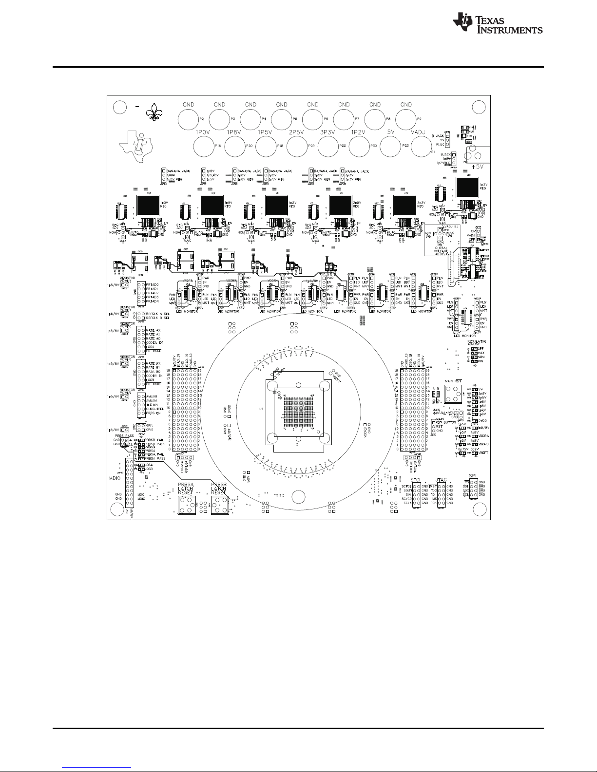
TLK6002
N
J
REVNA
6519192
EVM
+
+
+
+
+
+
TLK6002EVM Board Layouts
16 TLK6002EVM Board Layouts
www.ti.com
Figure 46. Top Signal, Layer 1
60
TLK6002 Dual-Channel, 0.47-Gbps to 6.25-Gbps, Multi-Rate Transceiver SLLU132–October 2010
Evaluation Module
Copyright © 2010, Texas Instruments Incorporated
Submit Documentation Feedback
Page 61
www.ti.com
TLK6002EVM Board Layouts
Figure 47. Internal Ground, Layers 2,4,6,8,10
SLLU132–October 2010 TLK6002 Dual-Channel, 0.47-Gbps to 6.25-Gbps, Multi-Rate Transceiver
Submit Documentation Feedback
Evaluation Module
61
Copyright © 2010, Texas Instruments Incorporated
Page 62
1p5/8V
(EntirePlane)
TLK6002EVM Board Layouts
www.ti.com
62
TLK6002 Dual-Channel, 0.47-Gbps to 6.25-Gbps, Multi-Rate Transceiver SLLU132–October 2010
Evaluation Module
Figure 48. Internal Power, Layer 3
Submit Documentation Feedback
Copyright © 2010, Texas Instruments Incorporated
Page 63
www.ti.com
TLK6002EVM Board Layouts
SLLU132–October 2010 TLK6002 Dual-Channel, 0.47-Gbps to 6.25-Gbps, Multi-Rate Transceiver
Submit Documentation Feedback
Figure 49. Internal Signal, Layer 5
63
Evaluation Module
Copyright © 2010, Texas Instruments Incorporated
Page 64

1p2V
3p3V
TLK6002EVM Board Layouts
www.ti.com
64
TLK6002 Dual-Channel, 0.47-Gbps to 6.25-Gbps, Multi-Rate Transceiver SLLU132–October 2010
Evaluation Module
Figure 50. Internal Signal, Layer 7
Submit Documentation Feedback
Copyright © 2010, Texas Instruments Incorporated
Page 65

5V
VDDRB
VDDRA
www.ti.com
TLK6002EVM Board Layouts
SLLU132–October 2010 TLK6002 Dual-Channel, 0.47-Gbps to 6.25-Gbps, Multi-Rate Transceiver
Submit Documentation Feedback
Figure 51. Internal Power, Layer 9
65
Evaluation Module
Copyright © 2010, Texas Instruments Incorporated
Page 66

TLK6002EVM Board Layouts
www.ti.com
Figure 52. Internal Ground and Power, Layers 11,13,15,17
66
TLK6002 Dual-Channel, 0.47-Gbps to 6.25-Gbps, Multi-Rate Transceiver SLLU132–October 2010
Evaluation Module
Copyright © 2010, Texas Instruments Incorporated
Submit Documentation Feedback
Page 67

2p5V
www.ti.com
TLK6002EVM Board Layouts
SLLU132–October 2010 TLK6002 Dual-Channel, 0.47-Gbps to 6.25-Gbps, Multi-Rate Transceiver
Submit Documentation Feedback
Figure 53. Internal Signal, Layer 12
67
Evaluation Module
Copyright © 2010, Texas Instruments Incorporated
Page 68

1p2V
TLK6002EVM Board Layouts
www.ti.com
68
TLK6002 Dual-Channel, 0.47-Gbps to 6.25-Gbps, Multi-Rate Transceiver SLLU132–October 2010
Evaluation Module
Figure 54. Internal Signal, Layer 14
Submit Documentation Feedback
Copyright © 2010, Texas Instruments Incorporated
Page 69

1p0V
DVDD
VDDRA
VREFT
2p5V
1p5/8V
Header
2p5V
www.ti.com
TLK6002EVM Board Layouts
Figure 55. Internal Power, Layer 16
SLLU132–October 2010 TLK6002 Dual-Channel, 0.47-Gbps to 6.25-Gbps, Multi-Rate Transceiver
Submit Documentation Feedback
Copyright © 2010, Texas Instruments Incorporated
Evaluation Module
69
Page 70

TLK6002EVM Board Layouts
www.ti.com
70
TLK6002 Dual-Channel, 0.47-Gbps to 6.25-Gbps, Multi-Rate Transceiver SLLU132–October 2010
Evaluation Module
Figure 56. Bottom Signal, Layer 18
Submit Documentation Feedback
Copyright © 2010, Texas Instruments Incorporated
Page 71

www.ti.com
(1)
TLK6002EVM Board Layouts
Table 2. TLK6002EVM Layer Construction
Subclass Type Material Thickness Conductivity Dielectric Loss Width Impedance
Name (mil) (mho/cm) Constant Tangent (mil) (Ω)
SURFACE AIR
TOP CONDUCTOR COPPER 2.4 595900 1 0 9.5 47.903
DIELECTRIC FR-4 5 0 4.1 0.035
L2_GND PLANE COPPER 1.2 595900 1 0
DIELECTRIC FR-4 5 0 4.1 0.035
L3_PWR PLANE COPPER 1.2 595900 1 0
DIELECTRIC FR-4 5 0 4.1 0.035
L4_GND PLANE COPPER 1.2 595900 1 0
DIELECTRIC FR-4 7 0 4.1 0.035
L5_SIG CONDUCTOR COPPER 1.2 595900 1 0 6.0 50.337
DIELECTRIC FR-4 7 0 4.1 0.035
L6_GND PLANE COPPER 1.2 595900 1 0
DIELECTRIC FR-4 7 0 4.1 0.035
L7_SIG CONDUCTOR COPPER 1.2 595900 1 0 6.0 50.337
DIELECTRIC FR-4 7 0 4.1 0.035
L8_GND PLANE COPPER 1.2 595900 1 0
DIELECTRIC FR-4 4 0 4.1 0.035
L9_PWR PLANE COPPER 1.2 595900 1 0
DIELECTRIC FR-4 4 0 4.1 0.035
L10_GND PLANE COPPER 1.2 595900 1 0
DIELECTRIC FR-4 4 0 4.1 0.035
L11_GND PLANE COPPER 1.2 595900 1 0
DIELECTRIC FR-4 7 0 4.1 0.035
L12_SIG CONDUCTOR COPPER 1.2 595900 1 0 6.0 50.337
DIELECTRIC FR-4 7 0 4.1 0.035
L13_GND PLANE COPPER 1.2 595900 1 0
DIELECTRIC FR-4 7 0 4.1 0.035
L14_SIG CONDUCTOR COPPER 1.2 595900 1 0 6.0 50.337
DIELECTRIC FR-4 7 0 4.1 0.035
L15_GND PLANE COPPER 1.2 595900 1 0
DIELECTRIC FR-4 5 0 4.1 0.035
L16_PWR PLANE COPPER 1.2 595900 1 0
DIELECTRIC FR-4 5 0 4.1 0.035
L17_GND PLANE COPPER 1.2 595900 1 0
DIELECTRIC FR-4 5 0 4.1 0.035
BOTTOM CONDUCTOR COPPER 2.4 595900 1 0 9.5 47.903
SURFACE AIR
The Impedance is set to be slightly less than 50 Ω on the traces in order to compensate for slight over-etching during the
manufacturing process. The end impedance after etching should result in a 50-Ω Impedance. Always consult with your board
manufacturer for their process/design requirements to ensure the desired impedance is achieved.
(1)
SLLU132–October 2010 TLK6002 Dual-Channel, 0.47-Gbps to 6.25-Gbps, Multi-Rate Transceiver
Submit Documentation Feedback
Evaluation Module
71
Copyright © 2010, Texas Instruments Incorporated
Page 72

Evaluation Board/Kit Important Notice
Texas Instruments (TI) provides the enclosed product(s) under the following conditions:
This evaluation board/kit is intended for use for ENGINEERING DEVELOPMENT, DEMONSTRATION, OR EVALUATION
PURPOSES ONLY and is not considered by TI to be a finished end-product fit for general consumer use. Persons handling the
product(s) must have electronics training and observe good engineering practice standards. As such, the goods being provided are
not intended to be complete in terms of required design-, marketing-, and/or manufacturing-related protective considerations,
including product safety and environmental measures typically found in end products that incorporate such semiconductor
components or circuit boards. This evaluation board/kit does not fall within the scope of the European Union directives regarding
electromagnetic compatibility, restricted substances (RoHS), recycling (WEEE), FCC, CE or UL, and therefore may not meet the
technical requirements of these directives or other related directives.
Should this evaluation board/kit not meet the specifications indicated in the User’s Guide, the board/kit may be returned within 30
days from the date of delivery for a full refund. THE FOREGOING WARRANTY IS THE EXCLUSIVE WARRANTY MADE BY
SELLER TO BUYER AND IS IN LIEU OF ALL OTHER WARRANTIES, EXPRESSED, IMPLIED, OR STATUTORY, INCLUDING
ANY WARRANTY OF MERCHANTABILITY OR FITNESS FOR ANY PARTICULAR PURPOSE.
The user assumes all responsibility and liability for proper and safe handling of the goods. Further, the user indemnifies TI from all
claims arising from the handling or use of the goods. Due to the open construction of the product, it is the user’s responsibility to
take any and all appropriate precautions with regard to electrostatic discharge.
EXCEPT TO THE EXTENT OF THE INDEMNITY SET FORTH ABOVE, NEITHER PARTY SHALL BE LIABLE TO THE OTHER
FOR ANY INDIRECT, SPECIAL, INCIDENTAL, OR CONSEQUENTIAL DAMAGES.
TI currently deals with a variety of customers for products, and therefore our arrangement with the user is not exclusive.
TI assumes no liability for applications assistance, customer product design, software performance, or infringement of
patents or services described herein.
Please read the User’s Guide and, specifically, the Warnings and Restrictions notice in the User’s Guide prior to handling the
product. This notice contains important safety information about temperatures and voltages. For additional information on TI’s
environmental and/or safety programs, please contact the TI application engineer or visit www.ti.com/esh.
No license is granted under any patent right or other intellectual property right of TI covering or relating to any machine, process, or
combination in which such TI products or services might be or are used.
FCC Warning
This evaluation board/kit is intended for use for ENGINEERING DEVELOPMENT, DEMONSTRATION, OR EVALUATION
PURPOSES ONLY and is not considered by TI to be a finished end-product fit for general consumer use. It generates, uses, and
can radiate radio frequency energy and has not been tested for compliance with the limits of computing devices pursuant to part 15
of FCC rules, which are designed to provide reasonable protection against radio frequency interference. Operation of this
equipment in other environments may cause interference with radio communications, in which case the user at his own expense
will be required to take whatever measures may be required to correct this interference.
EVM Warnings and Restrictions
It is important to operate this EVM within the input voltage range of -0.3 V to 5.3 V and the output voltage range of -0.3 V to 3.3 V .
Exceeding the specified input range may cause unexpected operation and/or irreversible damage to the EVM. If there are
questions concerning the input range, please contact a TI field representative prior to connecting the input power.
Applying loads outside of the specified output range may result in unintended operation and/or possible permanent damage to the
EVM. Please consult the EVM User's Guide prior to connecting any load to the EVM output. If there is uncertainty as to the load
specification, please contact a TI field representative.
During normal operation, some circuit components may have case temperatures greater than 50° C. The EVM is designed to
operate properly with certain components above 25° C as long as the input and output ranges are maintained. These components
include but are not limited to linear regulators, switching transistors, pass transistors, and current sense resistors. These types of
devices can be identified using the EVM schematic located in the EVM User's Guide. When placing measurement probes near
these devices during operation, please be aware that these devices may be very warm to the touch.
Mailing Address: Texas Instruments, Post Office Box 655303, Dallas, Texas 75265
Copyright © 2010, Texas Instruments Incorporated
Page 73

IMPORTANT NOTICE
Texas Instruments Incorporated and its subsidiaries (TI) reserve the right to make corrections, modifications, enhancements, improvements,
and other changes to its products and services at any time and to discontinue any product or service without notice. Customers should
obtain the latest relevant information before placing orders and should verify that such information is current and complete. All products are
sold subject to TI’s terms and conditions of sale supplied at the time of order acknowledgment.
TI warrants performance of its hardware products to the specifications applicable at the time of sale in accordance with TI’s standard
warranty. Testing and other quality control techniques are used to the extent TI deems necessary to support this warranty. Except where
mandated by government requirements, testing of all parameters of each product is not necessarily performed.
TI assumes no liability for applications assistance or customer product design. Customers are responsible for their products and
applications using TI components. To minimize the risks associated with customer products and applications, customers should provide
adequate design and operating safeguards.
TI does not warrant or represent that any license, either express or implied, is granted under any TI patent right, copyright, mask work right,
or other TI intellectual property right relating to any combination, machine, or process in which TI products or services are used. Information
published by TI regarding third-party products or services does not constitute a license from TI to use such products or services or a
warranty or endorsement thereof. Use of such information may require a license from a third party under the patents or other intellectual
property of the third party, or a license from TI under the patents or other intellectual property of TI.
Reproduction of TI information in TI data books or data sheets is permissible only if reproduction is without alteration and is accompanied
by all associated warranties, conditions, limitations, and notices. Reproduction of this information with alteration is an unfair and deceptive
business practice. TI is not responsible or liable for such altered documentation. Information of third parties may be subject to additional
restrictions.
Resale of TI products or services with statements different from or beyond the parameters stated by TI for that product or service voids all
express and any implied warranties for the associated TI product or service and is an unfair and deceptive business practice. TI is not
responsible or liable for any such statements.
TI products are not authorized for use in safety-critical applications (such as life support) where a failure of the TI product would reasonably
be expected to cause severe personal injury or death, unless officers of the parties have executed an agreement specifically governing
such use. Buyers represent that they have all necessary expertise in the safety and regulatory ramifications of their applications, and
acknowledge and agree that they are solely responsible for all legal, regulatory and safety-related requirements concerning their products
and any use of TI products in such safety-critical applications, notwithstanding any applications-related information or support that may be
provided by TI. Further, Buyers must fully indemnify TI and its representatives against any damages arising out of the use of TI products in
such safety-critical applications.
TI products are neither designed nor intended for use in military/aerospace applications or environments unless the TI products are
specifically designated by TI as military-grade or "enhanced plastic." Only products designated by TI as military-grade meet military
specifications. Buyers acknowledge and agree that any such use of TI products which TI has not designated as military-grade is solely at
the Buyer's risk, and that they are solely responsible for compliance with all legal and regulatory requirements in connection with such use.
TI products are neither designed nor intended for use in automotive applications or environments unless the specific TI products are
designated by TI as compliant with ISO/TS 16949 requirements. Buyers acknowledge and agree that, if they use any non-designated
products in automotive applications, TI will not be responsible for any failure to meet such requirements.
Following are URLs where you can obtain information on other Texas Instruments products and application solutions:
Products Applications
Amplifiers amplifier.ti.com Audio www.ti.com/audio
Data Converters dataconverter.ti.com Automotive www.ti.com/automotive
DLP® Products www.dlp.com Communications and www.ti.com/communications
DSP dsp.ti.com Computers and www.ti.com/computers
Clocks and Timers www.ti.com/clocks Consumer Electronics www.ti.com/consumer-apps
Interface interface.ti.com Energy www.ti.com/energy
Logic logic.ti.com Industrial www.ti.com/industrial
Power Mgmt power.ti.com Medical www.ti.com/medical
Microcontrollers microcontroller.ti.com Security www.ti.com/security
RFID www.ti-rfid.com Space, Avionics & www.ti.com/space-avionics-defense
RF/IF and ZigBee® Solutions www.ti.com/lprf Video and Imaging www.ti.com/video
Mailing Address: Texas Instruments, Post Office Box 655303, Dallas, Texas 75265
Copyright © 2010, Texas Instruments Incorporated
Telecom
Peripherals
Defense
Wireless www.ti.com/wireless-apps
 Loading...