

www.ti.com
FEATURES
1
2
3
4
5
6
7
8
9
10
30
29
28
27
26
25
24
23
22
21
11 121314
15 16
17
18 19
20
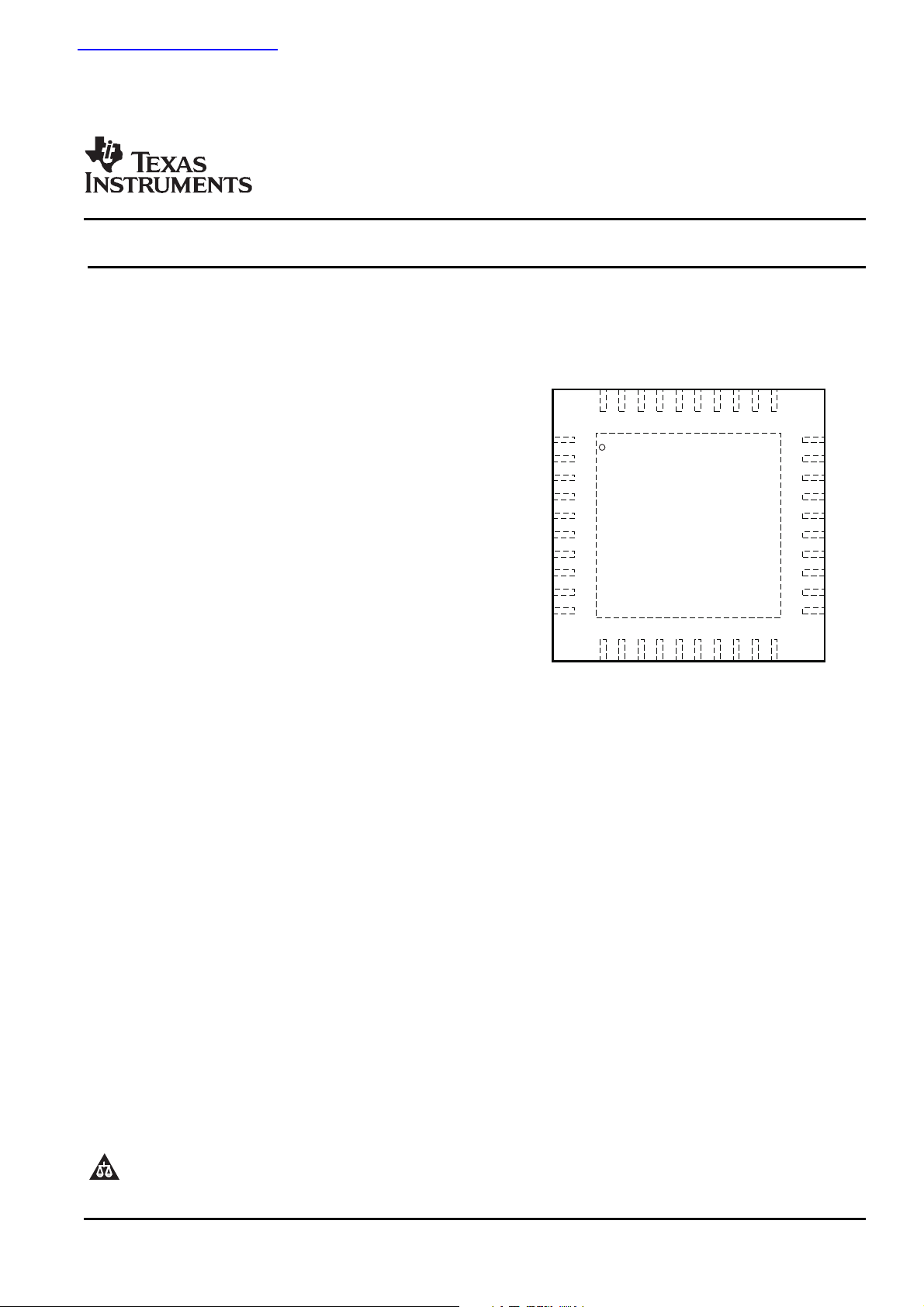
40 39 38 37 36
RHA Package
(TopView)
35 34 33 32 31
ENABLE
TD0
TD1
TD2
TD3
VDD
TD4
TD5
TD6
TD7
SYNC
RD0
RD1
RD2
VDD
RD3
RD4
RD5
RD6
RD7
GNDA
TXN
TXP
VDDA
VDDPLL
GNDA
RXP
RXN
SYNCEN
PRBSEN
GND
TD8
TD9
RBCMODE
REFCLK
LOOPEN
VDD
RBC0
RD9
RD8
RBC1
DESCRIPTION
TLK1221
SLLS713 – FEBRUARY 2007
ETHERNET TRANSCEIVER
• 0.6- to 1.3-Gigabits Per Second (Gbps)
Serializer/Deserializer
• Low Power Consumption 250 mW (typ) at 1.25
Gbps
• LVPECL-Compatible Differential I/O on
High-Speed Interface
• Single Monolithic PLL Design
• Support For 10-Bit Interface
• Receiver Differential-Input Thresholds,
200-mV Minimum
• Industrial Temperature Range From –40 ° C to
85 ° C
• IEEE 802.3 Gigabit Ethernet Compliant
• Designed in 0.25 µ m CMOS Technology
• No External Filter Capacitors Required
• Comprehensive Suite of Built-In Testability
• 2.5-V Supply Voltage for Lowest-Power
Operation
• 3.3-V Tolerant on LVTTL Inputs
• Hot Plug Protection
• 40-Pin 6-mm × 6-mm QFN PowerPAD™
Package
The TLK1221 gigabit Ethernet transceiver provides for high-speed full-duplex point-to-point data transmissions.
These devices are based on the timing requirements of the 10-bit interface specification by the IEEE 802.3
Gigabit Ethernet specification. The TLK1221 supports data rates from 0.6 Gbps through 1.3 Gbps.
The primary application of these devices is to provide building blocks for point-to-point baseband data
transmission over controlled-impedance media of 50 Ω . The transmission media can be printed-circuit board
traces, copper cables or fiber-optical media. The ultimate rate and distance of data transfer is dependent upon
the attenuation characteristics of the media and the noise coupling to the environment.
The TLK1221 performs the data serialization, deserialization, and clock extraction functions for a physical layer
interface device. The transceiver operates at 1.25 Gbps (typical), providing up to 1 Gbps of data bandwidth over
a copper or optical media interface.
This device supports the defined 10-bit interface (TBI). In the TBI mode, the serializer/deserializer (SERDES)
accepts 10-bit wide 8b/10b parallel encoded data bytes. The parallel data bytes are serialized and transmitted
differentially at PECL-compatible voltage levels. The SERDES extracts clock information from the input serial
stream and deserializes the data, outputting a parallel 10-bit data byte.
A comprehensive series of built-in tests is provided for self-test purposes, including loopback and pseudorandom
binary sequence (PRBS) generation and verification.
Please be aware that an important notice concerning availability, standard warranty, and use in critical applications of Texas
Instruments semiconductor products and disclaimers thereto appears at the end of this data sheet.
PowerPAD is a trademark of Texas Instruments.
All other trademarks are the property of their respective owners.
PRODUCTION DATA information is current as of publication date.
Copyright © 2007, Texas Instruments Incorporated
Products conform to specifications per the terms of the Texas
Instruments standard warranty. Production processing does not
necessarily include testing of all parameters.
查询TLK1221RHA供应商
www.ti.com
Differences Between TLK2201B, TLK2201BI, TLK1221, and TNETE2201
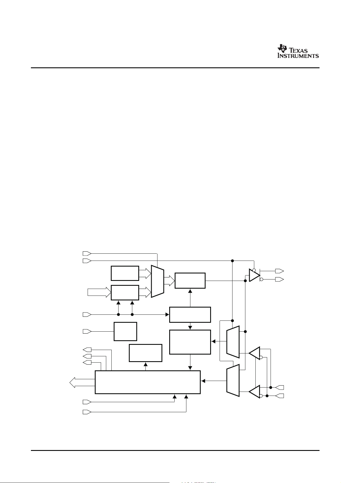
2:1
MUX
PRBS
Generator
10Bit
Registers
TD(0–9)
PRBSEN
LOOPEN
Parallelto
Serial
PhaseGenerator
Clock
REFCLK
Control
Logic
ENABLE
Interpolator
and
ClockExtraction
PRBS
Verification
SerialtoParallel
and
CommaDetect
Clock
RBC1
RBC0
SYNC/PASS
RD(0–9)
SYNCEN
2:1
MUX
2:1
MUX
Clock
Data
TXP
TXN
RXP
RXN
RBCMODE
TLK1221
SLLS713 – FEBRUARY 2007
The TLK1221 is housed in a high-performance, thermally enhanced, 40-pin QFN package. Use of this package
does not require any special considerations except to note that the pad, which is an exposed die pad on the
bottom of the device, is a metallic thermal and electrical conductor. It is required that the TLK1221 pad be
soldered to the thermal land on the board as it serves as the main ground connection for the device.
The TLK1221 is characterized for operation from –40 ° C to 85 ° C.
This device uses a 2.5-V supply. The I/O section is 3.3-V compatible. With the 2.5-V supply, the chipset is very
power-efficient, dissipating less than 200 mW typical power when operating at 1.25 Gbps.
The TLK1221 is designed to be hot-plug capable. A power-on reset causes RBC0, RBC1, the parallel output
signal terminals, TXP, and TXN to be held in the high-impedance state.
The TLK1221 is the functional equivalent of the TNETE2201. There are several differences between the devices
as noted below. Refer to Figure 12 in the application information section for an example of a typical application
circuit.
• V
CC
is 2.5 V for the TLK2201B, TLK2201BI, TLK1221, and TLK1201A vs 3.3 V for TNETE2201.
• The PLL filter capacitors on pins 16, 17, 48, and 49 of the TNETE2201 are no longer required. The
TLK2201B, TLK2201BI, TLK1221, and TLK1201A use these pins to provide added test capabilities. The
capacitors, if present, do not affect the operation of the device.
• No pulldown resistors are required on the TXP/TXN outputs.
• The TLK1221 is a QFN version of the TLK2201B optimized for GBE-only TBI-mode operation with no JTAG
functionality.
Functional Block Diagram
2
Submit Documentation Feedback
www.ti.com
Detailed Description
Transmission Latency
10-BitCode
TXP,TXN
REFCLK
t
d(Tx latency)
10-BitCode
b9
TD(0–9)
Data Reception
Receiver Clock Select Mode
TLK1221
SLLS713 – FEBRUARY 2007
In the TBI mode, the transmitter portion registers incoming 10-bit-wide data words (8b/10b encoded data,
TD0–TD9) on the rising edge of REFCLK. REFCLK is also used by the serializer, which multiplies the clock by a
factor of 10, providing a signal that is fed to the shift register. The 8b/10b encoded data is transmitted
sequentially, bits 0 through 9, over the differential high-speed I/O channel.
Data transmission latency is defined as the delay from the initial 10-bit word load to the serial transmission of
bit 9. The minimum latency in TBI mode is 19 bit times. The maximum latency in TBI mode is 20 bit times.
Figure 1. Transmitter Latency, Full-Rate Mode
The receiver section deserializes the differential serial data. The serial data is retimed based on an interpolated
clock generated from the reference clock. The serial data is then aligned to the 10-bit word boundaries and
presented to the protocol controller along with the receive byte clocks (RBC0, RBC1).
The TLK1221 only supports TBI-mode operation with half-rate and full-rate clocks on RBC0 and RBC1. In TBI
mode, there are two user-selectable clock modes that are controlled by the RBCMODE terminal: 1) full-rate
clock on RBC0 and 2) half-rate clocks on RBC0 and RBC1.
Table 1. Mode Selection
RECEIVE BYTE CLOCK
RBCMODE MODE
TLK1221
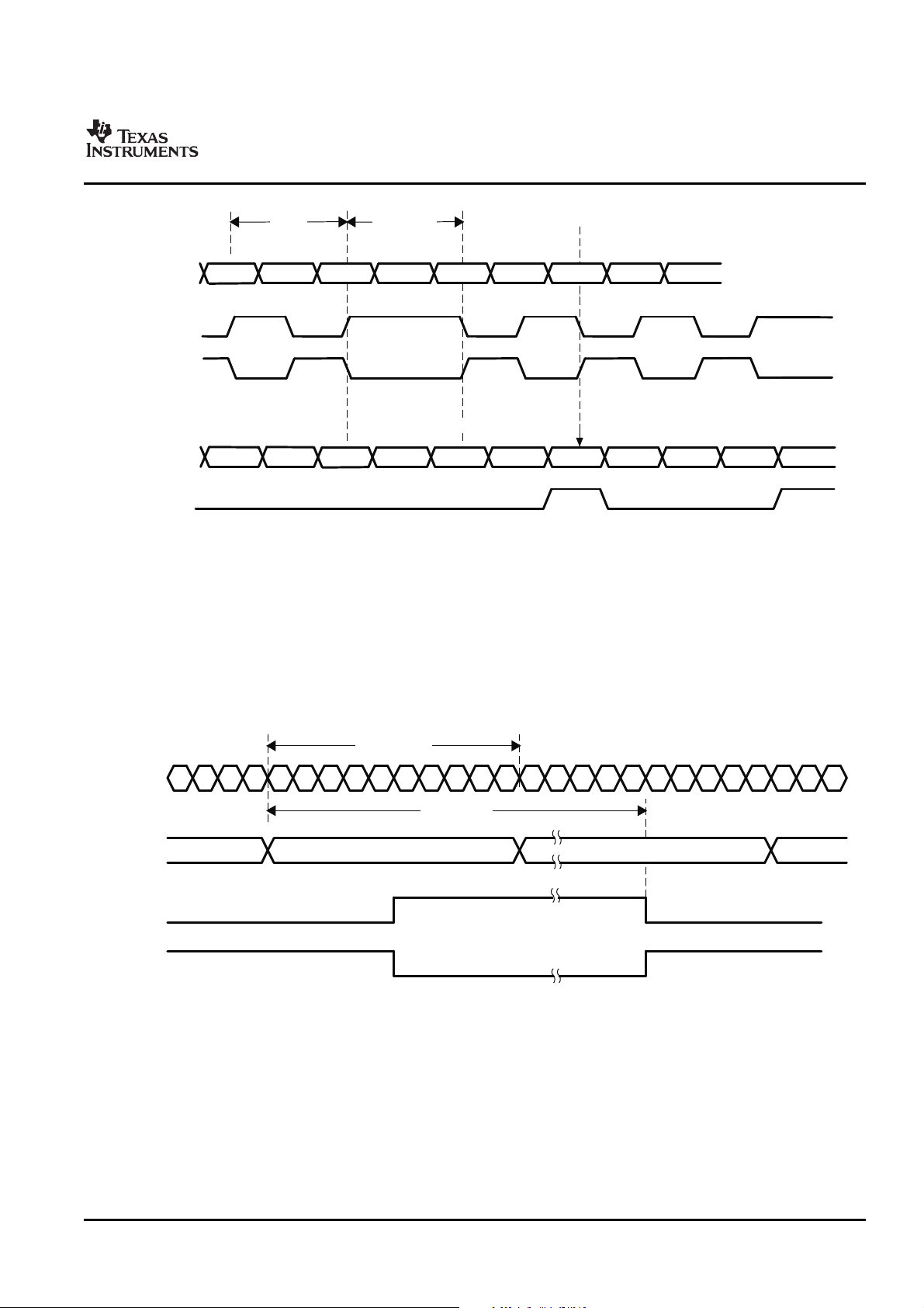
0 TBI half-rate 30–65 MHz
1 TBI full-rate 60–130 MHz
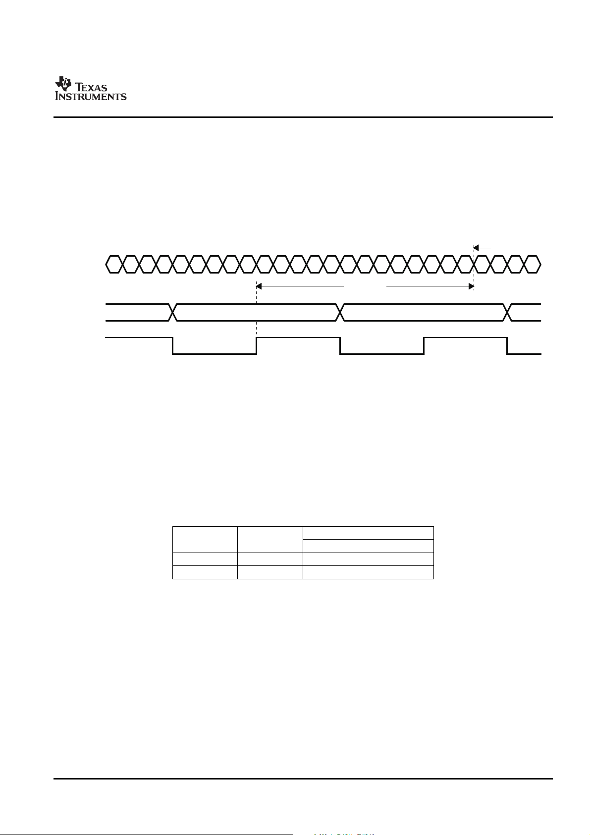
In the half-rate mode, two receive byte clocks (RBC0 and RBC1) are 180 degrees out of phase and operate at
one-half the data rate. The clocks are generated by dividing down the recovered clock. The received data is
output with respect to the two receive byte clocks (RBC0, RBC1), allowing a protocol device to clock the parallel
bytes using the RBC0 and RBC1 rising edges. For the outputs to the protocol device, byte 0 of the received data
is valid on the rising edge of RBC1. Refer to the timing diagram shown in Figure 2 .
3
Submit Documentation Feedback
www.ti.com
t
d(S)
t
d(S)
t
d(H)
t
d(H)
K28.5
DXX.X
DXX.X DXX.X
K28.5
DXX.X
RBC0
RBC1
SYNC
RD(0–9)
t
d(H)
t
d(S)
K28.5
DXX.X DXX.X DXX.X
K28.5
DXX.X
RBC0
SYNC
RD(0–9)
Receiver Word Alignment
TLK1221
SLLS713 – FEBRUARY 2007
Figure 2. Synchronous Timing Characteristic Waveforms (TBI Half-Rate Mode)
The receiver clock interpolator can lock to the incoming data without the need for a lock-to-reference preset. The
received serial data rate (RXP and RXN) is at the same baud rate as the transmitted data stream, ± 0.02% (200
PPM) for proper operation.
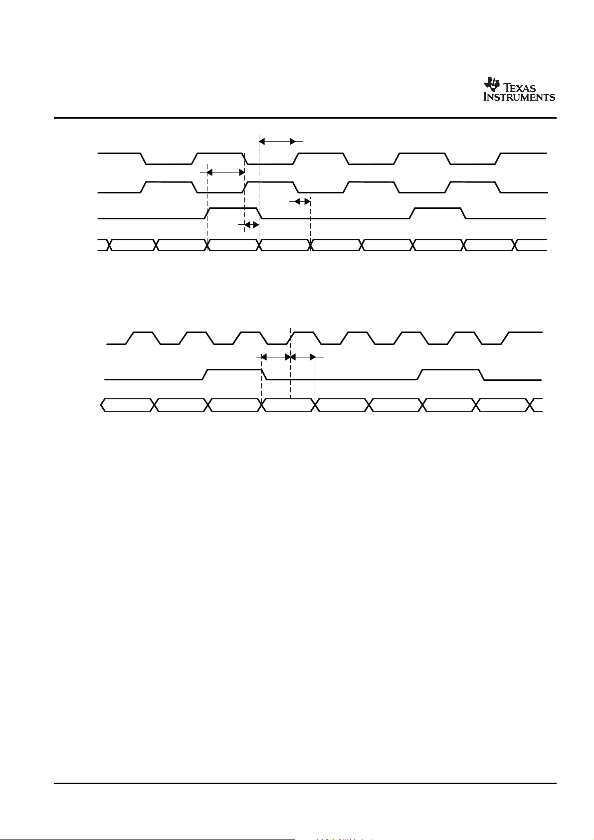
Figure 3. Synchronous Timing Characteristic Waveforms (TBI Full-Rate Mode)
These devices use the IEEE 802.3 Gigabit Ethernet defined 10-bit K28.5 character, which contains the 7-bit
comma-pattern word alignment scheme. The following sections explain how this scheme works and how it
realigns to the proper byte boundary of the data.
Comma Character on Expected Boundary
These devices provide 10-bit K28.5 character recognition and word alignment. The 10-bit word alignment is
enabled by forcing the SYNCEN terminal high. This enables the function that examines and compares serial
input data to the 7-bit synchronization pattern. The K28.5 character is defined by the 8b/10b coding scheme as a
pattern consisting of 0011 1110 10 (a negative number beginning with disparity), with the 7 MSBs (0011 111)
referred to as the comma character. The K28.5 character was implemented specifically for aligning data words.
As long as the K28.5 character falls within the expected 10-bit boundary, the received 10-bit data is properly
aligned and data realignment is not required. Figure 2 shows the timing characteristics of RBC0, RBC1, SYNC
and RD0–RD9 while synchronized. (Note: the K28.5 character is valid on the rising edge of RBC1).
Comma Character Not on Expected Boundary
If synchronization is enabled and a K28.5 character straddles the expected 10-bit word boundary, then word
realignment is necessary. Realignment or shifting the 10-bit word boundary truncates the character following the
misaligned K28.5, but the following K28.5 and all subsequent data is aligned properly as shown in Figure 4 . The
RBC0 and RBC1 pulse widths are stretched or stalled in their current state during realignment. With this design,
the maximum stretch that occurs is 20 bit times. This occurs during a worst-case scenario when the K28.5 is
aligned to the falling edge of RBC1 instead of the rising edge. Figure 4 shows the timing characteristics of the
data realignment.
4
Submit Documentation Feedback
www.ti.com
DXX.X
K28.5
DXX.X DXX.X
K28.5K28.5
DXX.X DXX.XDXX.X DXX.X
DXX.X
K28.5
DXX.X DXX.X
K28.5K28.5
DXX.X DXX.X
31Bit
Times
MaxReceive
PathLatency
WorstCase
MisalignedK28.5
MisalignmentCorrected
INPUTDATA
RBC0
RBC1
RD(0–9)
SYNC
CorruptData
30Bit
Times(Max)
Data Reception Latency
10-BitCode
RXP,RXN
RD(0–9)
RBC0
10-BitCode
t
d(Rx latency)
RBC1
Testability
TLK1221
SLLS713 – FEBRUARY 2007
Figure 4. Word Realignment Timing Characteristic Waveforms
Systems that do not require framed data may disable byte alignment by tying SYNCEN low.
When a SYNC character is detected, the SYNC signal is brought high and is aligned with the K28.5 character.
The duration of the SYNC pulse is equal to the duration of the data.
The serial-to-parallel data latency is the time from when the first bit arrives at the receiver until it is output in the
aligned parallel word with RD0 received as the first bit. The minimum latency in TBI mode is 21 bit times and the
maximum latency is 31 bit times.
Figure 5. Receiver Latency, TBI Half-Rate Mode Shown
The loopback function provides for at-speed testing of the transmit/receive section of the circuitry. The enable
function allows for all circuitry to be disabled so that an Iddq test can be performed. The PRBS function also
allows for built-in self-test (BIST).
5
Submit Documentation Feedback
www.ti.com
Loopback Testing
ENABLE Function
PRBS Function
TLK1221
SLLS713 – FEBRUARY 2007
The transceiver can provide a self-test function by enabling (LOOPEN to high level) the internal loopback path.
Enabling this function causes serial transmitted data to be routed internally to the receiver. The parallel data
output can be compared to the parallel input data for functional verification. (The external differential output is
held in a high-impedance state during the loopback testing.)
When held low, ENABLE disables all quiescent power in both analog and digital circuitry. This allows an
ultralow-power idle state when the link is not active.
These devices have a built-in 27– 1 PRBS function. When the PRBSEN control bit is set high, the PRBS test is
enabled. A PRBS is generated and fed into the 10-bit parallel transmitter input bus. Data from the normal
parallel input source is ignored during PRBS test mode. The PRBS pattern is then fed through the transmit
circuitry as if it were normal data and sent out to the transmitter. The output can be sent to a bit error rate tester
(BERT) or to the receiver of another TLK1221. Because the PRBS is not really random and is really a
predetermined sequence of ones and zeros, the data can be captured and checked for errors by a BERT. These
devices also have a built-in BERT function on the receiver side that is enabled by PRBSEN. It can receive a
PRBS pattern and check for errors, and then report the errors by forcing the SYNC/PASS terminal low. The
PRBS testing supports two modes (normal and latched), which are controlled by the SYNCEN input. When
SYNCEN is low, the result of the PRBS bit-error-rate test is passed to the SYNC/PASS terminal. When
SYNCEN is high, the result of the PRBS verification is latched on the SYNC/PASS output (i.e., a single failure
forces SYNC/PASS to remain low).
Table 2. TERMINAL FUNCTIONS
TERMINAL
I/O DESCRIPTION
NAME NO.
SIGNAL
Differential output transmit. TXP and TXN are differential serial outputs that interface to a
TXP 38 PECL
copper or an optical I/F module. TXP and TXN are put in a high-impedance state when
TXN 39 O
LOOPEN is high and are active when LOOPEN is low.
RXP 34 PECL Differential input receive. RXP and RXN together are the differential serial input interface
RXN 33 I from a copper or an optical I/F module.
Reference clock. REFCLK is an external input clock that synchronizes the receiver and
transmitter interface (60 MHz to 130 MHz). The transmitter uses this clock to register the
REFCLK 14 I
input data (TD0–TD9) for serialization.
In the TBI mode that data is registered on the rising edge of REFCLK.
Transmit data. These inputs carry 10-bit parallel data output from a protocol device to the
transceiver for serialization and transmission. This 10-bit parallel data is clocked into the
TD0–TD9 2–5, 7–12 I
transceiver on the rising edge of REFCLK and transmitted as a serial stream with TD0 sent
as the first bit.
Receive data. These outputs carry 10-bit parallel data output from the transceiver to the
RD0–RD9 29–27, 25–19 O protocol layer. The data is referenced to terminals RBC0 and RBC1. RD0 is the first bit
received.
Receive byte clock. RBC0 and RBC1 are recovered clocks used for synchronizing the 10-bit
output data on RD0–RD9.
In the half-rate mode, the 10-bit output data words are valid on the rising edges of RBC0
RBC0 17 and RBC1. These clocks are adjusted to half-word boundaries in conjunction with
O
RBC1 18 synchronous detect. The clocks are always expanded during data realignment and never
slivered or truncated. RBC0 registers bytes 1 and 3 of received data. RBC1 registers bytes 0
and 2 of received data. In normal-rate mode, only RBC0 is valid and operates at 1/10th the
serial data rate. Data is aligned to the rising edge.
Receive clock mode select. When RBCMODE is low, half-rate clocks are output on RBC0
I
RBCMODE 13 and RBC1. When RBCMODE is high, a full baud-rate clock is output on RBC0, and RBC1 is
P/D
(1)
held low.
(1) P/D = Internal pulldown resistor
6
Submit Documentation Feedback
www.ti.com
ABSOLUTE MAXIMUM RATINGS
DISSIPATION RATINGS
TLK1221
SLLS713 – FEBRUARY 2007
Table 2. TERMINAL FUNCTIONS (continued)
TERMINAL
I/O DESCRIPTION
NAME NO.
Synchronous function enable. When SYNCEN is high, the internal synchronization function
I is activated. When this function is activated, the transceiver detects the comma pattern
SYNCEN 32
P/U
(2)
(0011 111 negative beginning disparity) in the serial data stream and realigns data on byte
boundaries if required. When SYNCEN is low, serial input data is unframed in RD0–RD9.
Synchronous detect. The SYNC output is asserted high upon detection of the comma
pattern in the serial data path. SYNC pulses are output only when SYNCEN is activated
SYNC/PASS 30 O
(asserted high). In PRBS test mode (PRBSEN = high), SYNC/PASS outputs the status of
the PRBS test results (high = pass).
TEST
Loop enable. When LOOPEN is high (active), the internal loopback path is activated. The
transmitted serial data is directly routed to the inputs of the receiver. This provides a self-test
I
LOOPEN 15 capability in conjunction with the protocol device. The TXP and TXN outputs are held in a
P/D
(3)
high-impedance state during the loopback test. LOOPEN is held low during standard
operational state with external serial outputs and inputs active.
PRBS enable. When PRBSEN is high, the PRBS generation circuitry is enabled. The PRBS
I verification circuit in the receive side is also enabled. A PRBS signal can be fed to the
PRBSEN 31
P/D
(3)
receive inputs and checked for errors, which are reported by the SYNC/PASS terminal
indicating low.
When this terminal is low, the device is disabled for Iddq testing. RD0–RD9, RBCn, TXP and
I
ENABLE 1 TXN are high-impedance. The pullup and pulldown resistors on any input are disabled.
P/D
(2)
When ENABLE is high, the device operates normally.
POWER
VDD 6, 16, 26 Supply Digital logic power. Provides power for all digital circuitry and digital I/O buffers
Analog power. VDDA provides power for the high-speed analog circuits, receiver, and
VDDA 37 Supply
transmitter.
VDDPLL 36 Supply PLL power. Provides power for the PLL circuitry. This terminal requires additional filtering.
GROUND
GNDA 35, 40 Ground Analog ground. GNDA provides a ground for the high-speed analog circuits, RX and TX.
GNDQFN PAD Ground Digital logic ground. Provides a ground for the logic circuits and digital I/O buffers
(2) P/U = Internal pullup resistor
(3) P/D = Internal pulldown resistor
over operating free-air temperature range (unless otherwise noted)
VALUE
(1)
UNIT
V
DD
Supply voltage
(2)
–0.3 to 3 V
V
I
Input voltage range at TTL terminals –0.5 to 4 V
V
I
Input voltage range at other terminals –0.3 to V
DD
+ 0.3 V
ESD Electrostatic discharge CDM: 1, HBM: 2 kV
T
stg
Storage temperature –65 to 150 ° C
T
A
Characterized free-air temperature range –40 to 85 ° C
(1) Stresses beyond those listed under "absolute maximum ratings" may cause permanent damage to the device. These are stress ratings
only, and functional operation of the device at these or any other conditions beyond those indicated under "recommended operating
conditions" is not implied. Exposure to absolute-maximum-rated conditions for extended periods may affect device reliability.
(2) All voltage values, except differential I/O bus voltages, are with respect to network ground terminal.
TA≤ 25 ° C DERATING FACTOR TA= 70 ° C TA= 85 ° C
PACKAGE
POWER RATING ABOVE TA= 25 ° C POWER RATING POWER RATING
RHA
(1) (2)
2.85 W 28 mW/ ° C 1.57 W 1.4 W
(1) The thermal resistance junction to ambient of the RHA package is 35 ° C/W measured on a high-K board.
(2) The thermal resistance junction-to-case (exposed pad) of the RHA package is 5 ° C/W.
7
Submit Documentation Feedback
www.ti.com
RECOMMENDED OPERATING CONDITIONS
REFERENCE CLOCK (REFCLK) TIMING REQUIREMENTS
TTL ELECTRICAL CHARACTERISTICS
TLK1221
SLLS713 – FEBRUARY 2007
over operating free-air temperature range (unless otherwise noted)
MIN NOM MAX UNIT
VDD,
V
DDA
, Supply voltage 2.3 2.5 2.7 V
V
DDPLL
IDD, I
DDA
, Frequency = 1.25 Gbps, PRBS pattern; ENABLE
Total supply current 113 mA
I
DDPLL
= 1, V
DD
, V
DDPLL
and V
DDA
= 2.7 V
P
D
Total power dissipation Frequency = 1.25 Gbps, PRBS pattern 235 305 mW
Total shutdown current (IDD+I
DDA
+
I
DDQ
Enable = 0; V
DD
, V
DDPLL
and V
DDA
= 2.7 V 1000 µ A
I
DDPLL
)
PLL Startup lock time VDD, V
DDA
= 2.5 V 500 µ s
T
A
Operating free-air temperature –40 85 ° C
over recommended operating conditions (unless otherwise noted)
PARAMETER TEST CONDITIONS MIN TYP MAX UNIT
Minimum data rate TYP – 0.01% 60 TYP + 0.01%
f Frequency MHz
Maximum data rate TYP – 0.01% 130 TYP + 0.01%
Accuracy –100 100 ppm
DC Duty cycle 40% 50% 60%
Jitter Random plus deterministic 40 ps
over recommended operating conditions (unless otherwise noted)
PARAMETER TEST CONDITIONS MIN TYP MAX UNIT
V
OH
High-level output voltage IOH= –400 µ A V
DD
– 0.2 2.3 V
V
OL
Low-level output voltage IOL= 1 mA GND 0.25 0.5 V
V
IH
High-level input voltage 1.7 3.6 V
V
IL
Low-level input voltage 0.8 V
I
IH
High-level input current V
DD
= 2.3 V, VIN= 2 V 40 µ A
I
IL
Low-level input current V
DD
= 2.3 V, VIN= 0.4 V –40 µ A
C
IN
Input capacitance 4 pF
8
Submit Documentation Feedback

www.ti.com
TRANSMITTER/RECEIVER CHARACTERISTICS
80%
50%
20%
t
r
t
r
t
f
t
f
80%
50%
20%
~
V
~
V
~
V
~
V
80%
20%
0V
~
1V
~
–1V
TX+
TX–
VOD
RXP,RXN
RD(0–9)
RBC0
10-BitCode
t
d(Rx latency)
10-BitCode
b0
b1 b2
b3
b4
b5
b6
b7
b8 b9
TLK1221
SLLS713 – FEBRUARY 2007
over recommended operating conditions (unless otherwise noted)
PARAMETER TEST CONDITIONS MIN TYP MAX UNIT
VOD = |TxD – TxN| Rt = 50 Ω 600 850 1100 mV
Transmit common mode voltage
V
(CM)
Rt = 50 Ω 1000 1250 1400 mV
range
Receiver input voltage requirement,
200 1600 mV
VID = |RxP – RxN|
Receiver common mode voltage
1000 1250 2250 mV
range, (RxP + RxN)/2
C
I
Receiver input capacitance 2 pF
Differential output jitter, random +
t
(TJ)
Serial data total jitter (peak-to-peak) deterministic, PRBS pattern, 0.24 UI
Rω= 125 MHz
Serial data deterministic jitter Differential output jitter, PRBS
t
(DJ)
0.12 UI
(peak-to-peak) pattern, Rω= 125 MHz
Differential signal rise, fall time (20% RL= 50 Ω , CL= 5 pF, see Figure 6
tr, t
f
100 250 ps
to 80%) and Figure 8
Serial data jitter tolerance minimum
Differential input jitter, random +
required eye opening, (per 0.25 UI
deterministic, Rω= 125 MHz
IEEE-802.3 specification)
Receiver data acquisition lock time
500 µ s
from power up
Data relock time from loss of
1024 Bit times
synchronization
t
d(Tx latency)
Tx latency See Figure 1 20 22 UI
t
d(Rx latency)
Rx latency See Figure 5 and Figure 7 18 24 UI
Figure 6. Differential and Common-Mode Output Voltage Definitions
Figure 7. Receiver Latency, TBI Normal Mode Shown
9
Submit Documentation Feedback

www.ti.com
CL
5pF
CL
5pF
50 W
50 W
t
r
t
f
CLOCK
80%
50%
20%
t
r
t
f
2V
0.8V
DATA
1.4V
LVTTL OUTPUT SWITCHING CHARACTERISTICS
TRANSMITTER TIMING REQUIREMENTS
TLK1221
SLLS713 – FEBRUARY 2007
Figure 8. Transmitter Test Setup
Figure 9. TTL Data I/O Valid Levels for AC Measurement
over recommended operating conditions (unless otherwise noted)
PARAMETER TEST CONDITIONS MIN TYP MAX UNIT
t
r(RBC)
Clock rise time 0.3 1.5 ns
t
f(RBC)
Clock fall time 0.3 1.5 ns
80% to 20% output voltage, C = 5 pF (see
Figure 9 )
t
r
Data rise time 0.3 1.5 ns
t
f
Data fall time 0.3 1.5 ns
TBI normal mode (see Figure 3 ), Rω= 125 MHz,
2.5 ns
data valid prior to RBC0 rising
Data setup time
t
su(d1)
(RD0–RD9)
TBI normal mode (see Figure 3 ), Rω= 61.44
5 ns
MHz, data valid prior to RBC0 rising
TBI normal mode (see Figure 3 ), Rω= 125 MHz,
2 ns
data valid after RBC0 rising
t
h(d1)
Data hold time (RD0–RD9)
TBI normal mode (see Figure 3 ), Rω= 61.44
4 ns
MHz, data valid after RBC0 rising
Data setup time TBI half-rate mode, Rω= 125 MHz (see
t
su(d3)
2.5 ns
(RD0–RD9) Figure 2 )
TBI half-rate mode, Rω= 125 MHz (see
t
h(d3)
Data hold time (RD0–RD9) 1.5 ns
Figure 2 )
over recommended operating conditions (unless otherwise noted)
PARAMETER TEST CONDITIONS MIN TYP MAX UNIT
t
su(d4)
Data setup time (TD0–TD9) 1.6 ns
t
h(d4)
Data hold time (TD0–TD9) 0.8 ns
tr, t
f
TD[0,9] data rise and fall time See Figure 9 2 ns
10
Submit Documentation Feedback

www.ti.com
TLK1221
SLLS713 – FEBRUARY 2007
Table 3. AVAILABLE OPTIONS
T
A
PACKAGE
QFN PLASTIC QUAD FLAT PACK (RHA)
–40 ° C to 85 ° C TLK1221RHA
11
Submit Documentation Feedback

www.ti.com
APPLICATION INFORMATION
8b/10b Transmission Code
TLK1221
SLLS713 – FEBRUARY 2007
The PCS maps GMII signals into ten-bit code groups and vice versa, using an 8b/10b block coding scheme. The
PCS uses the transmission code to improve the transmission characteristics of information to be transferred
across the link. The encoding defined by the transmission code ensures that sufficient transitions are present in
the PHY bit stream to make clock recovery possible in the receiver. Such encoding also greatly increases the
likelihood of detecting any single- or multiple-bit errors that may occur during transmission and reception of
information. The 8b/10b transmission code specified for use has a high transition density, is run length limited,
and is dc-balanced. The transition density of the 8b/10b symbols ranges from 3 to 8 transitions per symbol. The
definition of the 8b/10b transmission code is specified in IEEE 802.3 Gigabit Ethernet and ANSI X3.230-1994
(FC-PH), clause 11.
8b/10b transmission code uses letter notation describing the bits of an unencoded information octet. The bit
notation of A, B, C, D, E, F, G, H for an unencoded information octet is used in the description of the 8b/10b
transmission code-groups, where A is the LSB. Each valid code group has been given a name using the
following convention: /Dx.y/ for the 256 valid data code-groups and /Kx.y/ for the special control code-groups,
where y is the decimal value of bits EDCBA and x is the decimal value of bits HGF (noted as K<HGF.EDCBA>).
Thus, an octet value of FE representing a code-group value of K30.7 would be represented in bit notation as
111 11110.
12
Submit Documentation Feedback

www.ti.com
_
+
VDD
GND
5kW
5kW
7.5kW
RXP
RXN
GND
7.5kW
VDD
Z
0
Z
0
Z
0
Z
0
TXP
TXN
Transmitter Media Receiver
_
+
VDD
GND
5kW
5kW
7.5kW
RXP
RXN
GND
7.5kW
VDD
Z
0
Z
0
Z
0
Z
0
TXP
TXN
Transmitter Media Receiver
TLK1221
SLLS713 – FEBRUARY 2007
APPLICATION INFORMATION (continued)
Figure 10. High-Speed I/O Directly Coupled Mode
Figure 11. High-Speed I/O AC-Coupled Mode
13
Submit Documentation Feedback
www.ti.com
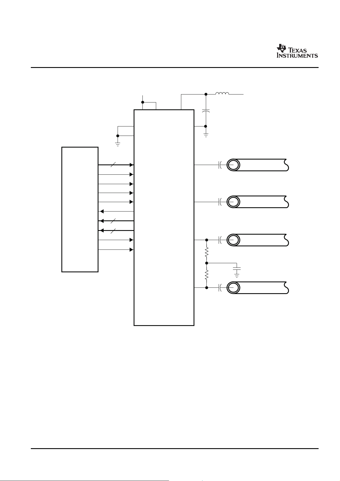
GNDQFN
GNDA
TD0–TD9
REFCLK
PRBSEN
14
31
SYNCEN
32
SYNC/PASS
30
10
10
RD0–RD9
2
RBC0–RBC1
ENABLE
1
LOOPEN
RCBMODE
15
13
Host
Protocol
Device
VDD VDDA
2.5V
VDDPLL
GNDA
5 at100MHzW
2.5V
40
38
Controlled-Impedance
TransmissionLine
TXP
39
Controlled-Impedance
TransmissionLine
TXN
34
Controlled-Impedance
TransmissionLine
RXP
33
Controlled-Impedance
TransmissionLine
RXN
Rt
Rt
50
W
50
W
TLK1221
0.01µF
TLK1221
SLLS713 – FEBRUARY 2007
APPLICATION INFORMATION (continued)
Figure 12. Typical Application Circuit (AC Mode)
14
Submit Documentation Feedback

PACKAGING INFORMATION
Orderable Device Status
(1)
Package
Type
Package
Drawing
Pins Package
Qty
Eco Plan
(2)
Lead/Ball Finish MSL Peak Temp
(3)
TLK1221RHAR ACTIVE QFN RHA 40 2500 Green (RoHS &
no Sb/Br)
CU NIPDAU Level-3-260C-168 HR
TLK1221RHARG4 ACTIVE QFN RHA 40 2500 Green (RoHS &
no Sb/Br)
CU NIPDAU Level-3-260C-168 HR
TLK1221RHAT ACTIVE QFN RHA 40 250 Green (RoHS &
no Sb/Br)
CU NIPDAU Level-3-260C-168 HR
TLK1221RHATG4 ACTIVE QFN RHA 40 250 Green (RoHS &
no Sb/Br)
CU NIPDAU Level-3-260C-168 HR
(1)
The marketing status values are defined as follows:
ACTIVE: Product device recommended for new designs.
LIFEBUY: TI has announced that the device will be discontinued, and a lifetime-buy period is in effect.
NRND: Not recommended for new designs. Device is in production to support existing customers, but TI does not recommend using this part in
a new design.
PREVIEW: Device has been announced but is not in production. Samples may or may not be available.
OBSOLETE: TI has discontinued the production of the device.
(2)
Eco Plan - The planned eco-friendly classification: Pb-Free (RoHS), Pb-Free (RoHS Exempt), or Green (RoHS & no Sb/Br) - please check
http://www.ti.com/productcontent for the latest availability information and additional product content details.
TBD: The Pb-Free/Green conversion plan has not been defined.
Pb-Free (RoHS): TI's terms "Lead-Free" or "Pb-Free" mean semiconductor products that are compatible with the current RoHS requirements
for all 6 substances, including the requirement that lead not exceed 0.1% by weight in homogeneous materials. Where designed to be soldered
at high temperatures, TI Pb-Free products are suitable for use in specified lead-free processes.
Pb-Free (RoHS Exempt): This component has a RoHS exemption for either 1) lead-based flip-chip solder bumps used between the die and
package, or 2) lead-based die adhesive used between the die and leadframe. The component is otherwise considered Pb-Free (RoHS
compatible) as defined above.
Green (RoHS & no Sb/Br): TI defines "Green" to mean Pb-Free (RoHS compatible), and free of Bromine (Br) and Antimony (Sb) based flame
retardants (Br or Sb do not exceed 0.1% by weight in homogeneous material)
(3)
MSL, Peak Temp. -- The Moisture Sensitivity Level rating according to the JEDEC industry standard classifications, and peak solder
temperature.
Important Information and Disclaimer:The information provided on this page represents TI's knowledge and belief as of the date that it is
provided. TI bases its knowledge and belief on information provided by third parties, and makes no representation or warranty as to the
accuracy of such information. Efforts are underway to better integrate information from third parties. TI has taken and continues to take
reasonable steps to provide representative and accurate information but may not have conducted destructive testing or chemical analysis on
incoming materials and chemicals. TI and TI suppliers consider certain information to be proprietary, and thus CAS numbers and other limited
information may not be available for release.
In no event shall TI's liability arising out of such information exceed the total purchase price of the TI part(s) at issue in this document sold by TI
to Customer on an annual basis.
PACKAGE OPTION ADDENDUM
www.ti.com
16-Mar-2007
Addendum-Page 1


IMPORTANT NOTICE
Texas Instruments Incorporated and its subsidiaries (TI) reserve the right to make corrections, modifications,
enhancements, improvements, and other changes to its products and services at any time and to
discontinue any product or service without notice. Customers should obtain the latest relevant information
before placing orders and should verify that such information is current and complete. All products are sold
subject to TI’s terms and conditions of sale supplied at the time of order acknowledgment.
TI warrants performance of its hardware products to the specifications applicable at the time of sale in
accordance with TI’s standard warranty. Testing and other quality control techniques are used to the extent
TI deems necessary to support this warranty. Except where mandated by government requirements, testing
of all parameters of each product is not necessarily performed.
TI assumes no liability for applications assistance or customer product design. Customers are responsible
for their products and applications using TI components. To minimize the risks associated with customer
products and applications, customers should provide adequate design and operating safeguards.
TI does not warrant or represent that any license, either express or implied, is granted under any TI patent
right, copyright, mask work right, or other TI intellectual property right relating to any combination, machine,
or process in which TI products or services are used. Information published by TI regarding third-party
products or services does not constitute a license from TI to use such products or services or a warranty or
endorsement thereof. Use of such information may require a license from a third party under the patents or
other intellectual property of the third party, or a license from TI under the patents or other intellectual
property of TI.
Reproduction of information in TI data books or data sheets is permissible only if reproduction is without
alteration and is accompanied by all associated warranties, conditions, limitations, and notices.
Reproduction of this information with alteration is an unfair and deceptive business practice. TI is not
responsible or liable for such altered documentation.
Resale of TI products or services with statements different from or beyond the parameters stated by TI for
that product or service voids all express and any implied warranties for the associated TI product or service
and is an unfair and deceptive business practice. TI is not responsible or liable for any such statements.
Following are URLs where you can obtain information on other Texas Instruments products and application
solutions:
Products
Applications
Amplifiers amplifier.ti.com Audio www.ti.com/audio
Data Converters dataconverter.ti.com Automotive www.ti.com/automotive
DSP dsp.ti.com Broadband www.ti.com/broadband
Interface interface.ti.com Digital Control www.ti.com/digitalcontrol
Logic logic.ti.com Military www.ti.com/military
Power Mgmt power.ti.com Optical Networking www.ti.com/opticalnetwork
Microcontrollers microcontroller.ti.com Security www.ti.com/security
Low Power Wireless www.ti.com/lpw Telephony www.ti.com/telephony
Video & Imaging www.ti.com/video
Wireless www.ti.com/wireless
Mailing Address: Texas Instruments
Post Office Box 655303 Dallas, Texas 75265
Copyright © 2007, Texas Instruments Incorporated

PACKAGING INFORMATION
Orderable Device Status
(1)
Package
Type
Package
Drawing
Pins Package
Qty
Eco Plan
(2)
Lead/Ball Finish MSL Peak Temp
(3)
TLK1221RHAR ACTIVE QFN RHA 40 2500 Green (RoHS &
no Sb/Br)
CU NIPDAU Level-3-260C-168 HR
TLK1221RHARG4 ACTIVE QFN RHA 40 2500 Green (RoHS &
no Sb/Br)
CU NIPDAU Level-3-260C-168 HR
TLK1221RHAT ACTIVE QFN RHA 40 250 Green (RoHS &
no Sb/Br)
CU NIPDAU Level-3-260C-168 HR
TLK1221RHATG4 ACTIVE QFN RHA 40 250 Green (RoHS &
no Sb/Br)
CU NIPDAU Level-3-260C-168 HR
(1)
The marketing status values are defined as follows:
ACTIVE: Product device recommended for new designs.
LIFEBUY: TI has announced that the device will be discontinued, and a lifetime-buy period is in effect.
NRND: Not recommended for new designs. Device is in production to support existing customers, but TI does not recommend using this part in
a new design.
PREVIEW: Device has been announced but is not in production. Samples may or may not be available.
OBSOLETE: TI has discontinued the production of the device.
(2)
Eco Plan - The planned eco-friendly classification: Pb-Free (RoHS), Pb-Free (RoHS Exempt), or Green (RoHS & no Sb/Br) - please check
http://www.ti.com/productcontent for the latest availability information and additional product content details.
TBD: The Pb-Free/Green conversion plan has not been defined.
Pb-Free (RoHS): TI's terms "Lead-Free" or "Pb-Free" mean semiconductor products that are compatible with the current RoHS requirements
for all 6 substances, including the requirement that lead not exceed 0.1% by weight in homogeneous materials. Where designed to be soldered
at high temperatures, TI Pb-Free products are suitable for use in specified lead-free processes.
Pb-Free (RoHS Exempt): This component has a RoHS exemption for either 1) lead-based flip-chip solder bumps used between the die and
package, or 2) lead-based die adhesive used between the die and leadframe. The component is otherwise considered Pb-Free (RoHS
compatible) as defined above.
Green (RoHS & no Sb/Br): TI defines "Green" to mean Pb-Free (RoHS compatible), and free of Bromine (Br) and Antimony (Sb) based flame
retardants (Br or Sb do not exceed 0.1% by weight in homogeneous material)
(3)
MSL, Peak Temp. -- The Moisture Sensitivity Level rating according to the JEDEC industry standard classifications, and peak solder
temperature.
Important Information and Disclaimer:The information provided on this page represents TI's knowledge and belief as of the date that it is
provided. TI bases its knowledge and belief on information provided by third parties, and makes no representation or warranty as to the
accuracy of such information. Efforts are underway to better integrate information from third parties. TI has taken and continues to take
reasonable steps to provide representative and accurate information but may not have conducted destructive testing or chemical analysis on
incoming materials and chemicals. TI and TI suppliers consider certain information to be proprietary, and thus CAS numbers and other limited
information may not be available for release.
In no event shall TI's liability arising out of such information exceed the total purchase price of the TI part(s) at issue in this document sold by TI
to Customer on an annual basis.
PACKAGE OPTION ADDENDUM
www.ti.com
16-Mar-2007
Addendum-Page 1


 Loading...