

www.ti.com
FEATURES
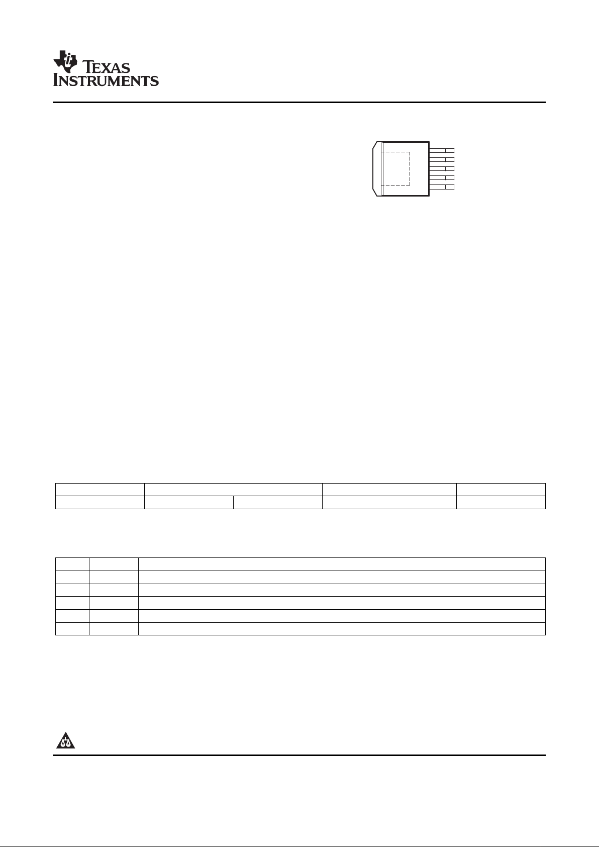
KTT PACKAGE
(TOP VIEW)
IN
1
RESET
GND
DELAY
OUT
5
4
3
2
DESCRIPTION/ORDERING INFORMATION
TLE4275-Q1
5-V LOW-DROPOUT VOLTAGE REGULATOR
SLVS647A – AUGUST 2006 – REVISED APRIL 2007
• Qualified for Automotive Applications
• Output Voltage 5 V ± 2%
• Very Low Current Consumption
• Power-On and Undervoltage Reset
• Reset Low-Level Output Voltage < 1 V
• Very Low Dropout Voltage
• Short-Circuit Proof
• Reverse-Polarity Proof
• ESD Protection > 6 kV
The TLE4275 is a monolithic integrated low-dropout voltage regulator offered in a 5-pin TO package. An input
voltage up to 45 V is regulated to V
OUT
= 5 V (typ). The device can drive loads up to 450 mA and is short-circuit
proof. At overtemperature, the TLE4275 is turned off by the incorporated temperature protection. A reset signal
is generated for an output voltage, V
OUT,rt
, of 4.65 V (typ). The reset delay time can be programmed by the
external delay capacitor.
The input capacitor, C
IN
, compensates for line fluctuation. Using a resistor of approximately 1 Ω , in series with
C
IN
, dampens the oscillation of input inductivity and input capacitance. The output capacitor, C
OUT
, stabilizes the
regulation circuit. Stability is specified at C
OUT
≥ 22 µ F and ESR ≤ 5 Ω , within the operating temperature range.
The control amplifier compares a reference voltage to a voltage that is proportional to the output voltage and
drives the base of the series transistor via a buffer. Saturation control as a function of the load current prevents
any oversaturation of the power element. The device also incorporates a number of internal circuits for
protection against:
• Overload
• Overtemperature
• Reverse polarity
ORDERING INFORMATION
T
J
PACKAGE
(1)
ORDERABLE PART NUMBER TOP-SIDE MARKING
–40 ° C to 150 ° C TO-263 – KTT Reel of 500 TLE4275QKTTRQ1 TLE4275Q1
(1) Package drawings, standard packing quantities, thermal data, symbolization, and PCB design guidelines are available at
www.ti.com/sc/package.
TERMINAL FUNCTIONS
NO. NAME DESCRIPTION
1 IN Input. Connect to ground as close to device as possible, through a ceramic capacitor.
2 RESET Reset output. Open-collector output.
3 GND Ground. Internally connected to heatsink.
4 DELAY Reset delay. Connect to ground with a capacitor to set delay time.
5 OUT Output. Connect to ground with ≥ 22- µ F capacitor, ESR < 5 Ω at 10 kHz.
Please be aware that an important notice concerning availability, standard warranty, and use in critical applications of Texas
Instruments semiconductor products and disclaimers thereto appears at the end of this data sheet.
PRODUCTION DATA information is current as of publication date.
Copyright © 2006–2007, Texas Instruments Incorporated
Products conform to specifications per the terms of the Texas
Instruments standard warranty. Production processing does not
necessarily include testing of all parameters.
www.ti.com
Reset
Generator
IN
OUT
DELAY
RESET
1
5
2
4
3
Saturation
Control and
Protection
Circuit
Temperature
Sensor
Bandgap
Reference
GND
Absolute Maximum Ratings
(1)
Recommended Operating Conditions
TLE4275-Q1
5-V LOW-DROPOUT VOLTAGE REGULATOR
SLVS647A – AUGUST 2006 – REVISED APRIL 2007
FUNCTIONAL BLOCK DIAGRAM
over operating free-air temperature range (unless otherwise noted)
MIN MAX UNIT
IN –42 45
V
I
Input voltage range
(2)
V
DELAY –0.3 7
OUT –1 16
V
O
Output voltage range V
RESET –0.3 25
I
I
Input current DELAY ± 2 mA
I
O
Output current RESET ± 5 mA
θ
JA
Package thermal impedance, junction to free air
(3) (4)
26.5 ° C/W
T
J
Operating junction temperature range –40 150 ° C
T
stg
Storage temperature range –65 150 ° C
(1) Stresses beyond those listed under "absolute maximum ratings" may cause permanent damage to the device. These are stress ratings
only, and functional operation of the device at these or any other conditions beyond those indicated under "recommended operating
conditions" is not implied. Exposure to absolute-maximum-rated conditions for extended periods may affect device reliability.
(2) All voltage values are with respect to the network ground terminal.
(3) Maximum power dissipation is a function of TJ(max), θJA, and TA. The maximum allowable power dissipation at any allowable ambient
temperature is PD= (TJ(max) – TA)/ θJA. Operating at the absolute maximum TJof 150 ° C can affect reliability.
(4) The package thermal impedance is calculated in accordance with JESD 51-7.
over operating free-air temperature range (unless otherwise noted)
MIN MAX UNIT
V
I
Input voltage 5.5 42 V
T
J
Junction temperature –40 150 ° C
2
Submit Documentation Feedback
www.ti.com
Electrical Characteristics
DV
O
DT
Switching Characteristics
TLE4275-Q1
5-V LOW-DROPOUT VOLTAGE REGULATOR
SLVS647A – AUGUST 2006 – REVISED APRIL 2007
over recommended operating free-air temperature range, VI= 13.5 V, TJ= –40 ° C to 150 ° C (unless otherwise noted)
(see Figure 1 )
PARAMETER TEST CONDITIONS MIN TYP MAX UNIT
IO= 5 mA to 400 mA, VI= 6 V to 28 V 4.9 5 5.1
V
O
Output voltage V
IO= 5 mA to 200 mA, VI= 6 V to 40 V 4.9 5 5.1
I
O
Output current limit 450 700 mA
TJ= 25 ° C 150 200
IO= 1 mA µ A
TJ≤ 85 ° C 150 220
Current consumption
I
q
Iq= II– I
O
IO= 250 mA 5 10
mA
IO= 400 mA 12 22
V
do
Dropout voltage
(1)
IO= 300 mA, Vdo= VI– V
O
250 500 mV
Load regulation IO= 5 mA to 400 mA 15 30 mV
Line regulation ∆ VI= 8 V to 32 V, IO= 5 mA –15 5 15 mV
PSSR Power-supply ripple rejection fr= 100 Hz, Vr= 0.5 V
pp
60 dB
Temperature output-voltage drift 0.5 mV/K
V
O,rt
RESET switching threshold 4.5 4.65 4.8 V
V
ROL
RESET output low voltage R
ext
≥ 5 k Ω , VO> 1 V 0.2 0.4 V
I
ROH
RESET output leakage current V
ROH
= 5 V 0 10 µ A
I
D,c
RESET charging current VD= 1 V 3 5.5 9 µ A
V
DU
RESET upper timing threshold 1.5 1.8 2.2 V
V
DRL
RESET lower timing threshold 0.2 0.4 0.7 V
(1) Measured when the output voltage VOhas dropped 100 mV from the nominal value obtained at VI= 13.5 V
over operating free-air temperature range (unless otherwise noted) (see Figure 2 )
PARAMETER TEST CONDITIONS MIN TYP MAX UNIT
t
rd
RESET delay time CD= 47 nF 10 16 22 ms
t
rr
RESET reaction time CD= 47 nF 0.5 2 µ s
3
Submit Documentation Feedback
www.ti.com
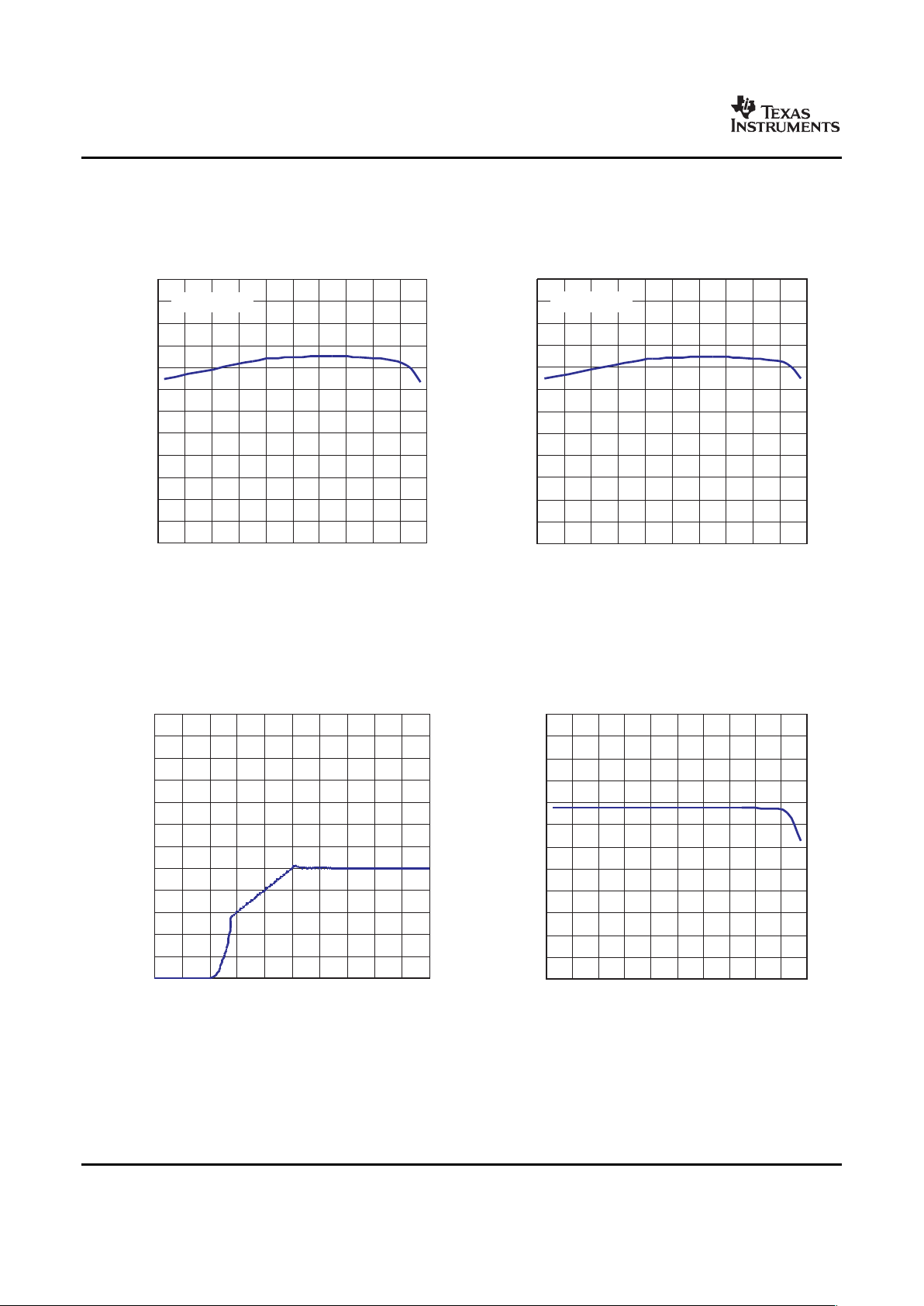
TYPICAL CHARACTERISTICS
4.6
4.7
4.8
4.9
5
5.1
5.2
-45 -25 -5 15 35 55 75 95 115 135 155
TJ– Junction Temperature – °C
V
O
– Output Voltage – V
VI= 6 V
4.6
4.7
4.8
4.9
5
5.1
5.2
-45 -25 -5 15 35 55 75 95 115 135 155
TJ– Junction Temperature – °C
V
O
– Output Voltage – V
VI= 28 V
0
1
2
3
4
5
6
7
8
9
10
11
12
0 1 2 3 4 5 6 7 8 9 10
V
I
– Input Voltage – V
V
O
– Output Voltage – V
0
100
200
300
400
500
600
700
800
900
1000
1100
1200
-45 -25 -5 15 35 55 75 95 115 135 155
TJ– Junction Temperature – °C
I
O
– Output Current – mA
TLE4275-Q1
5-V LOW-DROPOUT VOLTAGE REGULATOR
SLVS647A – AUGUST 2006 – REVISED APRIL 2007
OUTPUT VOLTAGE OUTPUT VOLTAGE
vs vs
JUNCTION TEMPERATURE JUNCTION TEMPERATURE
OUTPUT VOLTAGE OUTPUT CURRENT
vs vs
INPUT VOLTAGE JUNCTION TEMPERATURE
4
Submit Documentation Feedback
 Loading...