

Page 1
D
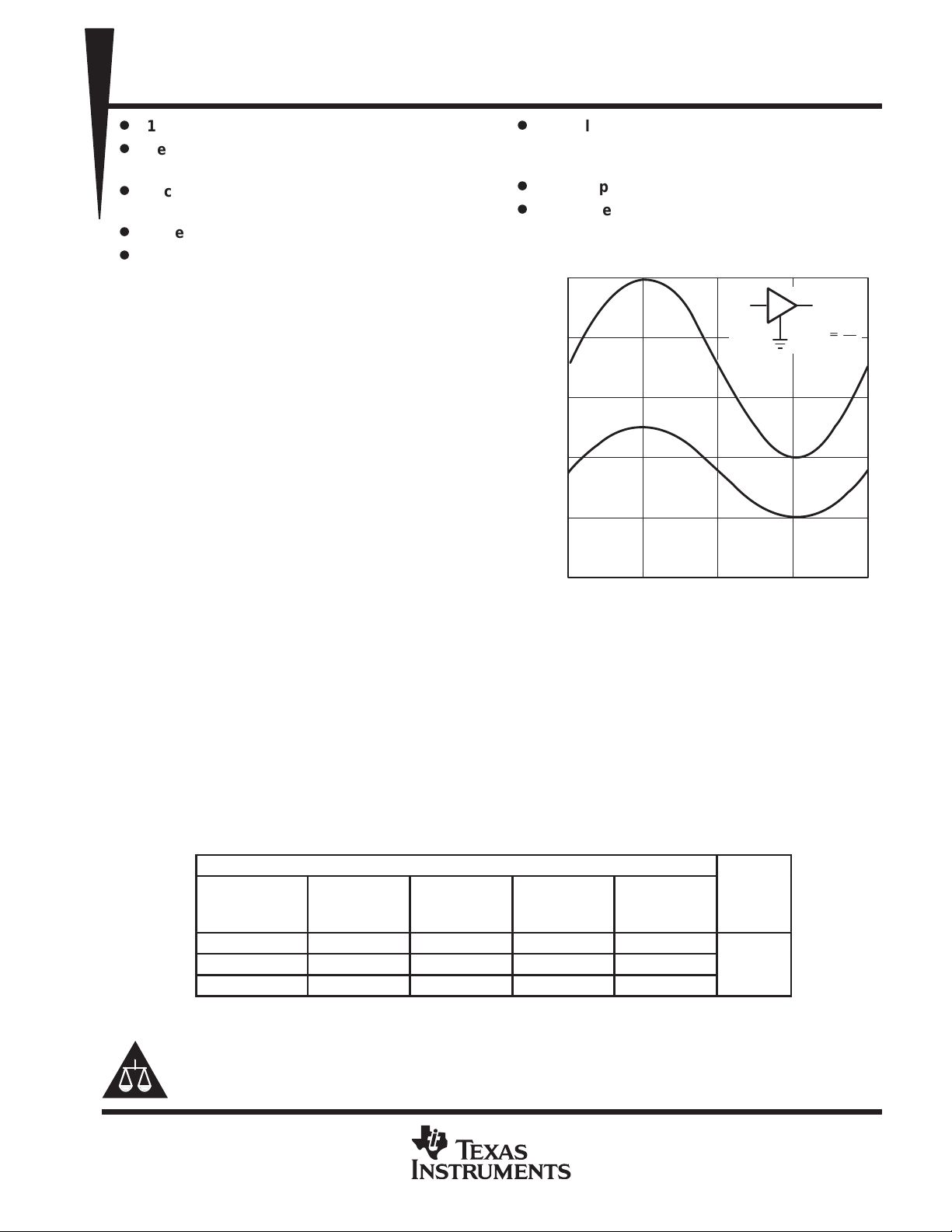
1/2 VI Virtual Ground for Analog Systems
D
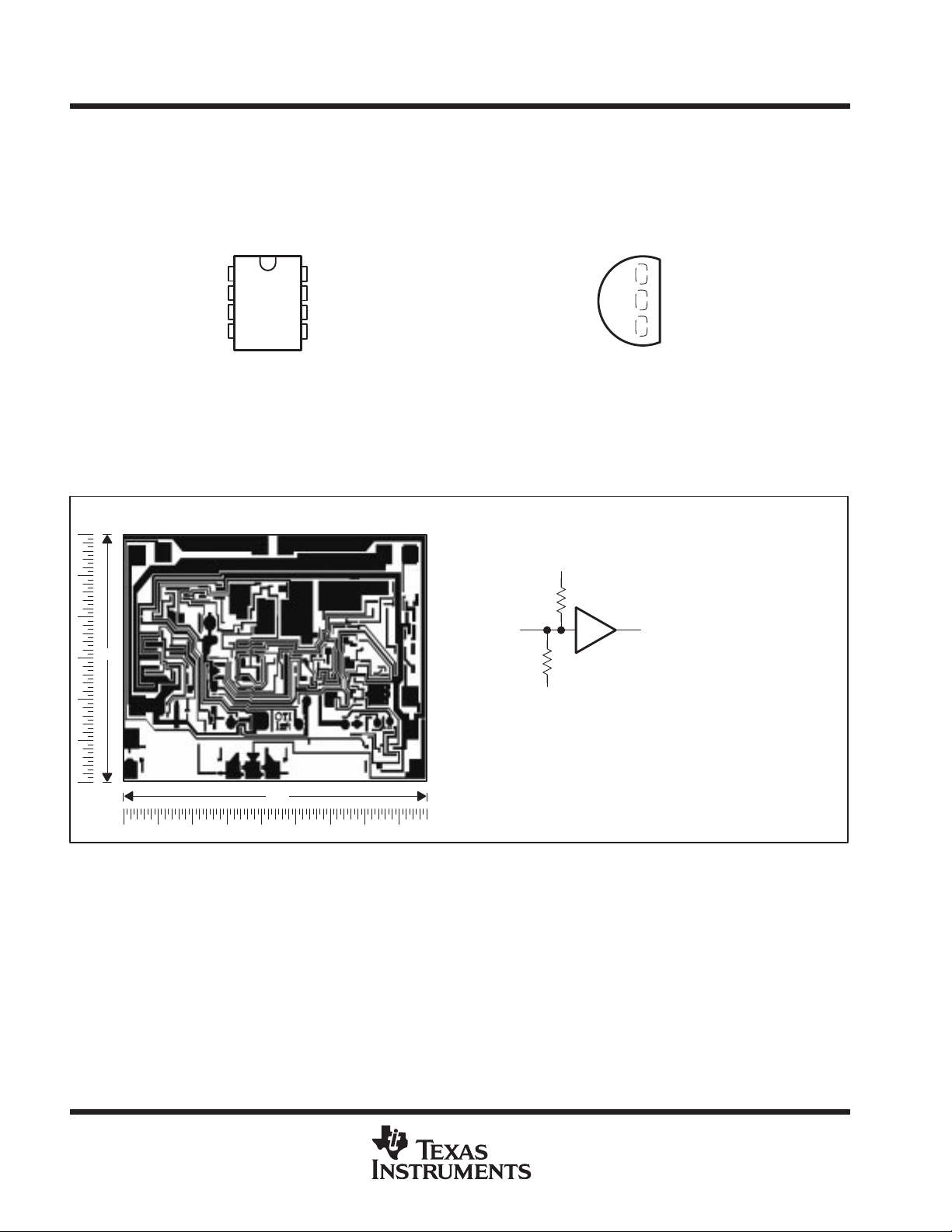
Self-Contained 3-terminal TO-226AA
Package
D
Micropower Operation...170 µA Typ,
V
= 5 V
I
D
Wide VI Range...4 V to 40 V
D
High Output-Current Capability
– Source...20 mA Typ
– Sink...20 mA Typ
description
In signal-conditioning applications utilizing a
single power source, a reference voltage equal to
one-half the supply voltage is required for
termination of all analog signal grounds. Texas
Instruments presents a precision virtual ground
whose output voltage is always equal to one-half
the input voltage, the TLE2426 “rail splitter.”
TLE2426, TLE2426Y
THE “RAIL SPLITTER”
PRECISION VIRTUAL GROUND
SLOS098D – AUGUST 1991 – REVISED MA Y 1998
D
Excellent Output Regulation
– –45 µV Typ at I
– +15 µV Typ at I
D
Low-Impedance Output...0.0075 Ω Typ
D
Noise Reduction Pin (D, JG, and P
Packages Only)
INPUT/OUTPUT TRANSFER CHARACTERISTICS
10
V
I
8
6
V
Voltage – V
4
O
= 0 to –10 mA
O
= 0 to +10 mA
O
V
I
V
O
VO+
V
I
2
The unique combination of a high-performance,
micropower operational amplifier and a precision-
2
trimmed divider on a single silicon chip results in
a precise V
sourcing current. The TLE2426 provides a lowimpedance output with 20 mA of sink and source
capability while drawing less than 280 µA
ratio of 0.5 while sinking and
O/VI
0
0 0.25 0.5 0.75 1
t – Time – s
of supply current over the full input range of 4 V to 40 V. A designer need not pay the price in terms of board
space for a conventional signal ground consisting of resistors, capacitors, operational amplifiers, and voltage
references. The performance and precision of the TLE2426 is available in an easy-to-use, space saving,
3-terminal LP package. For increased performance, the optional 8-pin packages provide a noise-reduction pin.
With the addition of an external capacitor (C
), peak-to-peak noise is reduced while line ripple rejection is
NR
improved.
Initial output tolerance for a single 5-V or 12-V system is better than 1% with 3.6% over the full 40-V input range.
Ripple rejection exceeds 12 bits of accuracy . Whether the application is for a data acquisition front end, analog
signal termination, or simply a precision voltage reference, the TLE2426 eliminates a major source of system
error.
AVAILABLE OPTIONS
PACKAGED DEVICES
SMALL
T
A
0°C to 70°C TLE2426CD — TLE2426CLP TLE2426CP
–40°C to 85°C TLE2426ID — TLE2426ILP TLE2426IP TLE2426Y
–55°C to 125°C TLE2426MD TLE2426MJG TLE2426MLP TLE2426MP
The D and LP packages are available taped and reeled in the commercial temperature range only. Add R suffix
to the device type (e. g., TLC2426CDR). Chips are tested at 25°C.
OUTLINE
(D)
CERAMIC
DIP
(JG)
PLASTIC
(LP)
PLASTIC
DIP
(P)
CHIP
FORM
(Y)
Please be aware that an important notice concerning availability, standard warranty, and use in critical applications of
Texas Instruments semiconductor products and disclaimers thereto appears at the end of this data sheet.
PRODUCTION DATA information is current as of publication date.
Products conform to specifications per the terms of Texas Instruments
standard warranty. Production processing does not necessarily include
testing of all parameters.
POST OFFICE BOX 655303 • DALLAS, TEXAS 75265
Copyright 1998, Texas Instruments Incorporated
1
Page 2
TLE2426, TLE2426Y
THE “RAIL SPLITTER”
PRECISION VIRTUAL GROUND
SLOS098D – AUGUST 1991 – REVISED MA Y 1998
description (continued)
The C-suffix devices are characterized for operation from 0°C to 70°C. The I suffix devices are characterized
for operation from –40°C to 85°C. The M suffix devices are characterized over the full military temperature range
of –55°C to 125°C.
D, JG, OR P PACKAGE
(TOP VIEW)
LP PACKAGE
(TOP VIEW)
OUT
COMMON
NC – No internal connection
IN
NC
1
2
3
4
NOISE REDUCTION
8
NC
7
NC
6
NC
5
IN
COMMON
OUT
TLE2426Y chip information
This chip, properly assembled, displays characteristics similar to the TLE2426C. Thermal compression or
ultrasonic bonding may be used on the doped aluminum bonding pads. The chips may be mounted with
conductive epoxy or a gold-silicon preform.
BONDING PAD ASSIGNMENTS
(2) (2)
(1)
(1)
NOISE
REDUCTION
IN
(8)
(2)
COMMON
(3)
+1
(1)
CHIP THICKNESS:
15 MILS TYPICAL
BONDING PADS:
4 × 4 MILS MINIMUM
OUT
TJmax = 150°C
TOLERANCES ARE ±10%.
ALL DIMENSIONS ARE IN
MILS.
60
(3)
(3)
(8)
88
2
POST OFFICE BOX 655303 • DALLAS, TEXAS 75265
NOTE A: Both bonding pads numbered 1, both numbered 2,
and both numbered 3, must be bonded out to the
corresponding functions pin.
Page 3
TLE2426, TLE2426Y
PACKAGE
UNIT
THE “RAIL SPLITTER”
PRECISION VIRTUAL GROUND
SLOS098D – AUGUST 1991 – REVISED MA Y 1998
absolute maximum ratings over operating free-air temperature (unless otherwise noted)
Continuous input voltage, V
40 V. . . . . . . . . . . . . . . . . . . . . . . . . . . . . . . . . . . . . . . . . . . . . . . . . . . . . . . . . . . . . . . . .
I
†
Continuous filter trap voltage 40 V. . . . . . . . . . . . . . . . . . . . . . . . . . . . . . . . . . . . . . . . . . . . . . . . . . . . . . . . . . . . . . . .
Output current, I
±80 mA. . . . . . . . . . . . . . . . . . . . . . . . . . . . . . . . . . . . . . . . . . . . . . . . . . . . . . . . . . . . . . . . . . . . . . .
O
Duration of short-circuit current at (or below) 25°C (see Note 1) unlimited. . . . . . . . . . . . . . . . . . . . . . . . . . . . . .
Continuous total power dissipation See Dissipation Rating Table. . . . . . . . . . . . . . . . . . . . . . . . . . . . . . . . . . . . .
Operating free-air temperature range, T
: C suffix 0°C to 70°C. . . . . . . . . . . . . . . . . . . . . . . . . . . . . . . . . . . . . .
A
I suffix –40°C to 85°C. . . . . . . . . . . . . . . . . . . . . . . . . . . . . . . . . . . . .
M suffix –55°C to 125°C. . . . . . . . . . . . . . . . . . . . . . . . . . . . . . . . . .
Storage temperature range, T
–65°C to 150°C. . . . . . . . . . . . . . . . . . . . . . . . . . . . . . . . . . . . . . . . . . . . . . . . . . .
stg
Lead temperature 1,6 mm (1/16 inch) from case for 10 seconds: D or P package 260°C. . . . . . . . . . . . . . . . .
Lead temperature 1,6 mm (1/16 inch) from case for 60 seconds: JG or LP package 300°C. . . . . . . . . . . . . .
†
Stresses beyond those listed under “absolute maximum ratings” may cause permanent damage to the device. These are stress ratings only, and
functional operation of the device at these or any other conditions beyond those indicated under “recommended operating conditions” is not
implied. Exposure to absolute-maximum-rated conditions for extended periods may affect device reliability.
NOTE 1: The output may be shorted to either supply. T emperature and/or supply voltages must be limited to ensure that the maximum dissipation
rating is not exceeded.
DISSIPATION RATING TABLE
TA ≤ 25°C DERATING FACTOR TA = 70°C TA = 85°C TA = 125°C
POWER RATING ABOVE TA = 25°C POWER RATING POWER RATING POWER RATING
D 725 mV 5.8 mW/°C 464 mW 377 mW 145 mW
JG 1050 mV 8.4 mW/°C 672 mW 546 mW 210 mW
LP 775 mV 6.2 mW/°C 496 mW 403 mW 155 mW
P 1000 mV 8.0 mW/°C 640 mW 520 mW 200 mW
recommended operating conditions
Input voltage, V
Operating free-air temperature, T
I
A
C SUFFIX I SUFFIX M SUFFIX
MIN MAX MIN MAX MIN MAX
4 40 4 40 4 40 V
0 70 –40 85 –55 125 °C
POST OFFICE BOX 655303 • DALLAS, TEXAS 75265
3
Page 4
TLE2426, TLE2426Y
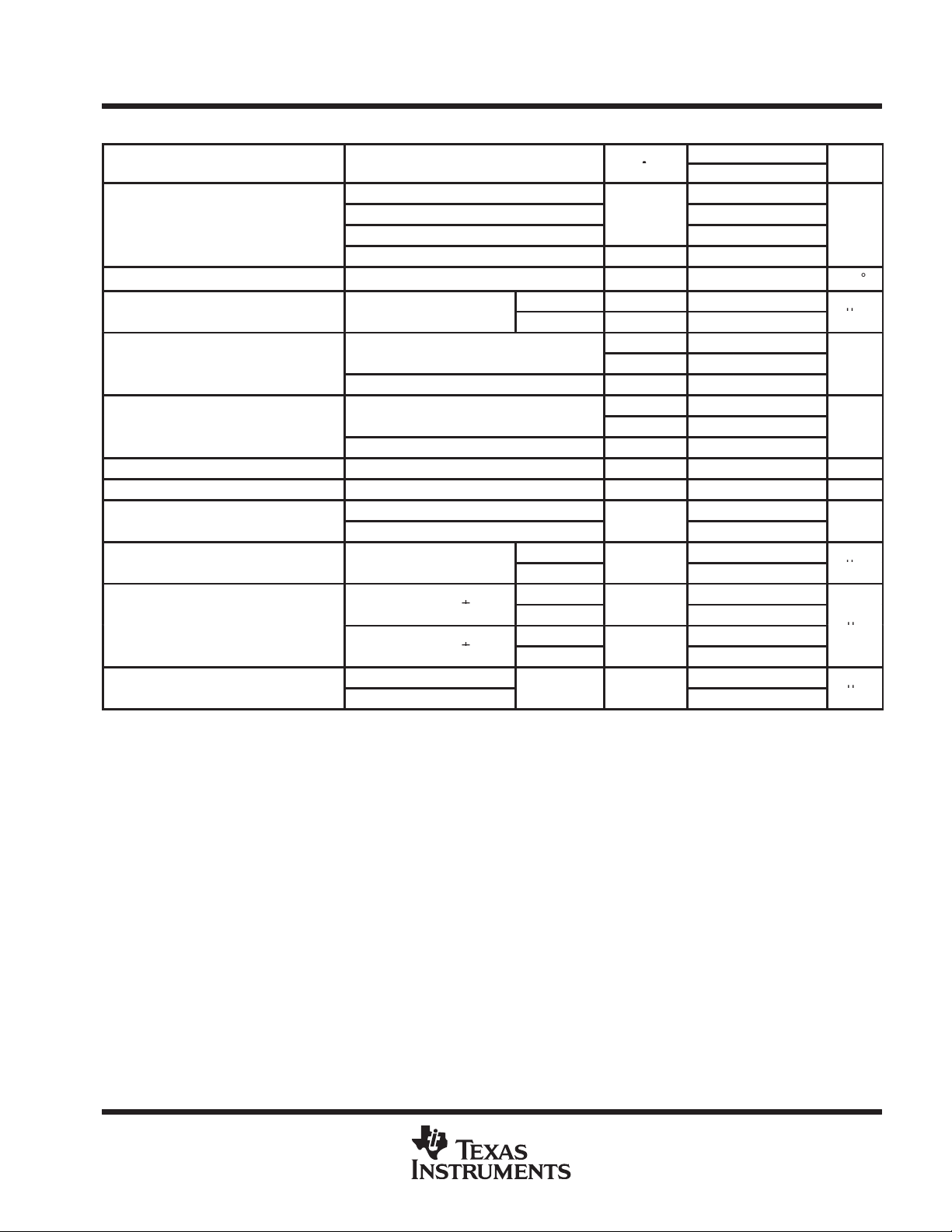
PARAMETER
TEST CONDITIONS
T
†
UNIT
Output voltage
V
Temperature coefficient of output voltage
Full range
25
ppm/°C
Supply current
No load
A
‡
I
mA
(sourcing current)
‡
‡
I
0 to 10 mA
(sinking current)
‡
Short-circuit current
25°C
mA
Output noise voltage, rms
f
25°C
V
V
I
±10 mA
25°C
Output voltage current step response
s
V
01%,I
±10 mA
25°C
Step response
C
100 pF
25°C
s
THE “RAIL SPLITTER”
PRECISION VIRTUAL GROUND
SLOS098D – AUGUST 1991 – REVISED MA Y 1998
electrical characteristics at specified free-air temperature, VI = 5 V , IO = 0 (unless otherwise noted)
A
VI = 4 V 1.98 2 2.02
p
p
pp
Output voltage regulation
Output voltage regulation
Output impedance 25°C 7.5 22.5 mΩ
Noise-reduction impedance 25°C 110 kΩ
p
p
p
p
†
Full range is 0°C to 70°C.
‡
The listed values are not production tested.
p
p
p
VI = 5 V
VI = 40 V 19.8 20 20.2
VI = 5 V Full range 2.475 2.525
VI = 5 V 25°C 170 300
VI = 4 to 40 V Full range 400
= 0 to –10
O
IO = 0 to –20 mA 25°C –150 ±450
=
O
IO = 0 to 20 mA 25°C 65 ±235
Sinking current, VO = 5 V
Sourcing current, VO = 0
= 10 Hz to 10 kHz
to 0.1%,
O
to 0.
O
VI = 0 to 5 V, VO to 0.1%
VI = 0 to 5 V, VO to 0.01%
O
O
=
=
CNR = 0
CNR = 1 µF
CL = 0
CL = 100 pF
CL = 0
CL = 100 pF
p
=
L
25°C
25°C –45 ±160
Full range ±250
25°C 15 ±160
Full range ±250
°
°
°
°
°
TLE2426C
MIN TYP MAX
2.48 2.5 2.52
26
–47
120
30
290
275
400
390
20
160
pp
µ
µV
µV
µ
µ
µ
4
POST OFFICE BOX 655303 • DALLAS, TEXAS 75265
Page 5
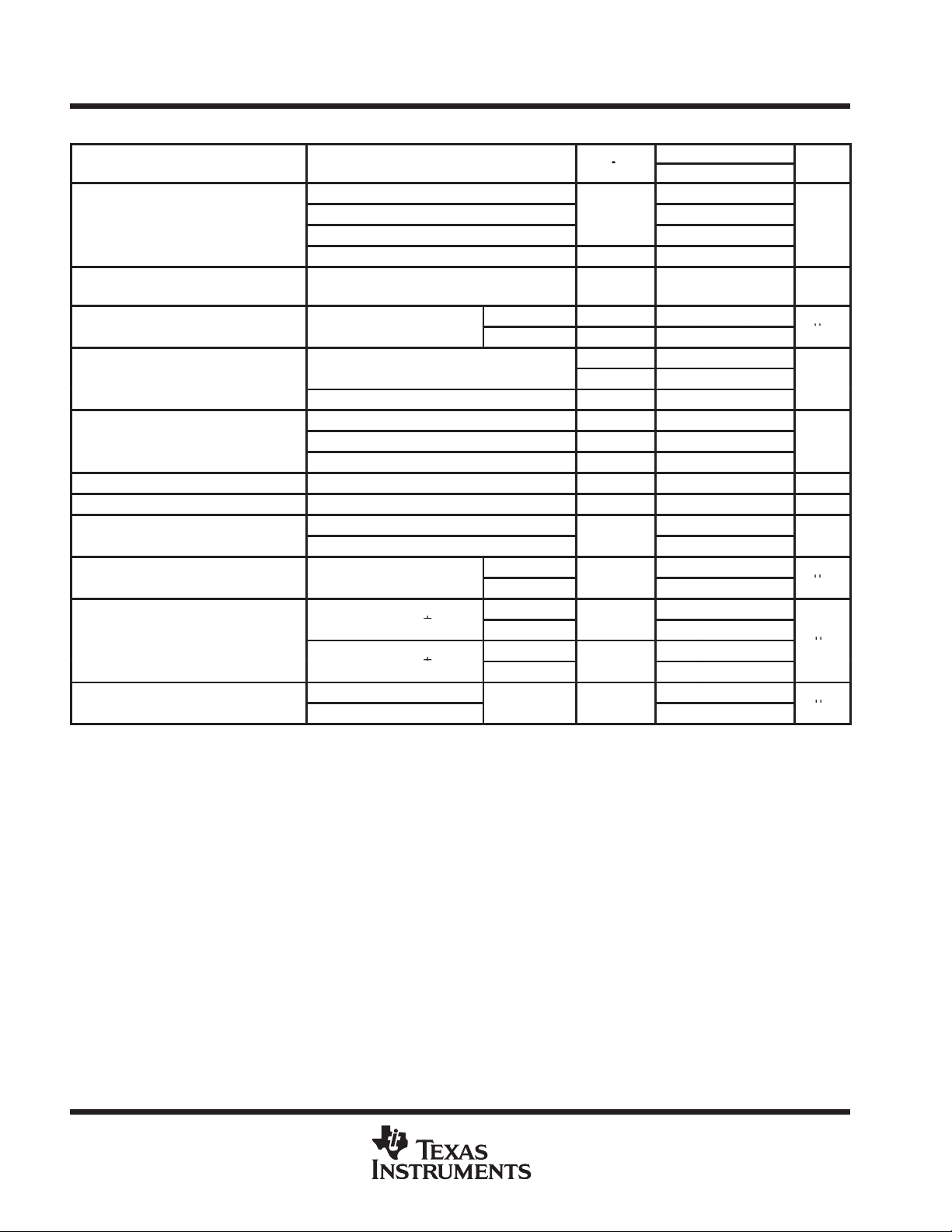
TLE2426, TLE2426Y
PARAMETER
TEST CONDITIONS
T
†
UNIT
Output voltage
V
Temperature coefficient of output voltage
Full range
35
ppm/°C
Supply current
No load
A
‡
I
mA
(sourcing current)
‡
‡
I
0 to 10 mA
(sinking current)
‡
Short-circuit current
25°C
mA
Output noise voltage, rms
f
25°C
V
V
I
±10 mA
25°C
Output voltage current step response
s
V
01%,I
±10 mA
25°C
Step response
C
100 pF
25°C
s
THE “RAIL SPLITTER”
PRECISION VIRTUAL GROUND
SLOS098D – AUGUST 1991 – REVISED MA Y 1998
electrical characteristics at specified free-air temperature, VI = 12 V , IO = 0 (unless otherwise noted)
A
VI = 4 V 1.98 2 2.02
p
p
pp
Output voltage regulation
Output voltage regulation
Output impedance 25°C 7.5 22.5 mΩ
Noise-reduction impedance 25°C 110 kΩ
p
p
p
p
†
Full range is 0°C to 70°C.
‡
The listed values are not production tested.
p
p
p
VI = 12 V
VI = 40 V 19.8 20 20.2
VI = 12 V Full range 5.945 6.055
VI = 12 V 25°C 195 300
VI = 4 to 40 V Full range 400
= 0 to –10
O
IO = 0 to –20 mA 25°C –150 ±450
=
O
IO = 0 to 20 mA 25°C 65 ±235
Sinking current, VO = 12 V
Sourcing current, VO = 0
= 10 Hz to 10 kHz
to 0.1%,
O
to 0.
O
VI = 0 to 12 V, VO to 0.1%
VI = 0 to 12 V, VO to 0.01%
=
O
=
O
CNR = 0
CNR = 1 µF
CL = 0
CL = 100 pF
CL = 0
CL = 100 pF
p
=
L
25°C
25°C –45 ±160
Full range ±250
25°C 15 ±160
Full range ±250
°
°
°
°
°
TLE2426C
MIN TYP MAX
5.95 6 6.05
31
–70
120
30
290
275
400
390
20
120
pp
µ
µV
µV
µ
µ
µ
POST OFFICE BOX 655303 • DALLAS, TEXAS 75265
5
Page 6
TLE2426, TLE2426Y
PARAMETER
TEST CONDITIONS
T
†
UNIT
Output voltage
V
Full range
25
ppm/°C
Supply current
No load
A
‡
I
mA
(sourcing current)
‡
‡
(sinking current)
‡
Short-circuit current
25°C
mA
Output noise voltage, rms
f
25°C
V
V
I
±10 mA
25°C
Output voltage current step response
s
V
01%,I
±10 mA
25°C
Step response
C
100 pF
25°C
s
THE “RAIL SPLITTER”
PRECISION VIRTUAL GROUND
SLOS098D – AUGUST 1991 – REVISED MA Y 1998
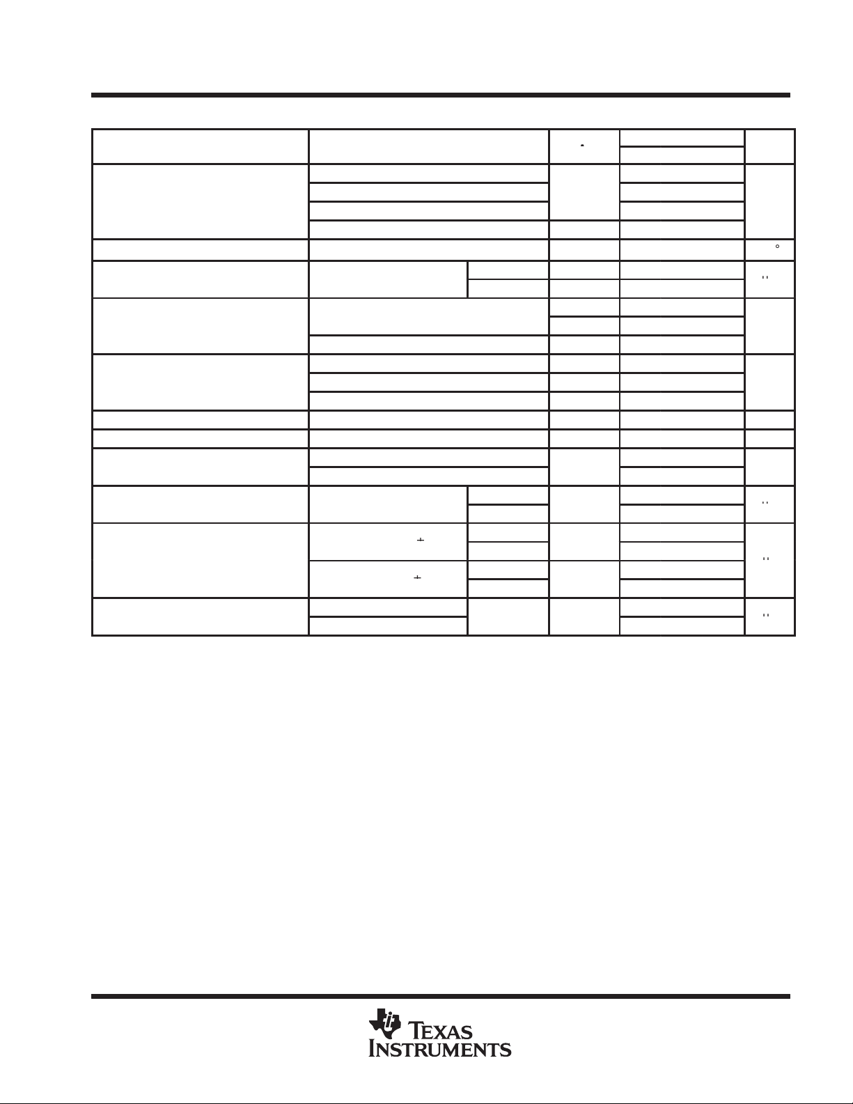
electrical characteristics at specified free-air temperature, VI = 5 V , IO = 0 (unless otherwise noted)
A
VI = 4 V 1.98 2 2.02
p
Temperature coefficient of output voltage
pp
Output voltage regulation
Output voltage regulation
Output impedance 25°C 7.5 22.5 mΩ
Noise-reduction impedance 25°C 110 kΩ
p
p
p
p
†
Full range is –40°C to 85°C.
‡
The listed values are not production tested.
p
p
VI = 5 V
VI = 40 V 19.8 20 20.2
VI = 5 V Full range 2.47 2.53
VI = 5 V 25°C 170 300
VI = 4 to 40 V Full range 400
= 0 to –10
O
IO = 0 to –20 mA 25°C –150 ±450
IO = 0 to 10 mA 25°C 15 ±160
IO = 0 to 8 mA Full range ±250
IO = 0 to 20 mA 25°C 65 ±235
Sinking current, VO = 5 V
Sourcing current, VO = 0
= 10 Hz to 10 kHz
to 0.1%,
O
to 0.
O
VI = 0 to 5 V, VO to 0.1%
VI = 0 to 5 V, VO to 0.01%
=
O
=
O
CNR = 0
CNR = 1 µF
CL = 0
CL = 100 pF
CL = 0
CL = 100 pF
p
=
L
25°C
25°C –45 ±160
Full range ±250
°
°
°
°
°
TLE2426I
MIN TYP MAX
2.48 2.5 2.52
26
–47
120
30
290
275
400
390
20
160
pp
°
µ
µV
µV
µ
µ
µ
6
POST OFFICE BOX 655303 • DALLAS, TEXAS 75265
Page 7
TLE2426, TLE2426Y
PARAMETER
TEST CONDITIONS
T
†
UNIT
Output voltage
V
Temperature coefficient of output voltage
Full range
35
ppm/°C
Supply current
No load
A
‡
I
mA
(sourcing current)
‡
‡
(sinking current)
‡
Short-circuit current
25°C
mA
Output noise voltage, rms
f
25°C
V
V
I
±10 mA
25°C
Output voltage current step response
s
V
01%,I
±10 mA
25°C
Step response
C
100 pF
25°C
s
THE “RAIL SPLITTER”
PRECISION VIRTUAL GROUND
SLOS098D – AUGUST 1991 – REVISED MA Y 1998
electrical characteristics at specified free-air temperature, VI = 12 V , IO = 0 (unless otherwise noted)
A
VI = 4 V 1.98 2 2.02
p
p
pp
Output voltage regulation
Output voltage regulation
Output impedance 25°C 7.5 22.5 mΩ
Noise-reduction impedance 25°C 110 kΩ
p
p
p
p
†
Full range is –40°C to 85°C.
‡
The listed values are not production tested.
p
p
p
VI = 12 V
VI = 40 V 19.8 20 20.2
VI = 12 V Full range 5.935 6.065
VI = 12 V 25°C 195 300
VI = 4 to 40 V Full range 400
= 0 to –10
O
IO = 0 to –20 mA 25°C –150 ±450
IO = 0 to 10 mA 25°C 15 ±160
IO = 0 to 8 mA Full range ±250
IO = 0 to 20 mA 25°C 65 ±235
Sinking current, VO = 12 V
Sourcing current, VO = 0
= 10 Hz to 10 kHz
to 0.1%,
O
to 0.
O
VI = 0 to 12 V, VO to 0.1%
VI = 0 to 12 V, VO to 0.01%
O
=
O
=
CNR = 0
CNR = 1 µF
CL = 0
CL = 100 pF
CL = 0
CL = 100 pF
p
=
L
25°C
25°C –45 ±160
Full range ±250
°
°
°
°
°
TLE2426I
MIN TYP MAX
5.95 6 6.05
31
–70
120
30
290
275
400
390
20
120
pp
µ
µV
µV
µ
µ
µ
POST OFFICE BOX 655303 • DALLAS, TEXAS 75265
7
Page 8

TLE2426, TLE2426Y
PARAMETER
TEST CONDITIONS
T
†
UNIT
Output voltage
V
Temperature coefficient of output voltage
Full range
25
ppm/°C
Supply current
No load
A
‡
I
mA
(sourcing current)
‡
‡
(sinking current)
‡
Short-circuit current
25°C
mA
Output noise voltage, rms
f
25°C
V
V
I
±10 mA
25°C
Output voltage current step response
s
V
01%,I
±10 mA
25°C
Step response
C
100 pF
25°C
s
THE “RAIL SPLITTER”
PRECISION VIRTUAL GROUND
SLOS098D – AUGUST 1991 – REVISED MA Y 1998
electrical characteristics at specified free-air temperature, VI = 5 V , IO = 0 (unless otherwise noted)
A
VI = 4 V 1.98 2 2.02
p
p
pp
Output voltage regulation
Output voltage regulation
Output impedance 25°C 7.5 22.5 mΩ
Noise-reduction impedance 25°C 110 kΩ
p
p
p
p
†
Full range is –55°C to 125°C.
‡
The listed values are not production tested.
p
p
p
VI = 5 V
VI = 40 V 19.8 20 20.2
VI = 5 V Full range 2.465 2.535
VI = 5 V 25°C 170 300
VI = 4 to 40 V Full range 400
= 0 to –10
O
IO = 0 to –20 mA 25°C –150 ±450
IO = 0 to 10 mA 25°C 15 ±160
IO = 0 to 3 mA Full range ±250
IO = 0 to 20 mA 25°C 65 ±235
Sinking current, VO = 5 V
Sourcing current, VO = 0
= 10 Hz to 10 kHz
to 0.1%,
O
to 0.
O
VI = 0 to 5 V, VO to 0.1%
VI = 0 to 5 V, VO to 0.01%
=
O
=
O
CNR = 0
CNR = 1 µF
CL = 0
CL = 100 pF
CL = 0
CL = 100 pF
p
=
L
25°C
25°C –45 ±160
Full range ±250
°
°
°
°
°
TLE2426M
MIN TYP MAX
2.48 2.5 2.52
26
–47
120
30
290
275
400
390
20
120
pp
µ
µV
µV
µ
µ
µ
8
POST OFFICE BOX 655303 • DALLAS, TEXAS 75265
Page 9

TLE2426, TLE2426Y
PARAMETER
TEST CONDITIONS
T
†
UNIT
Output voltage
V
Temperature coefficient of output voltage
Full range
35
ppm/°C
Supply current
No load
A
I
mA
(sourcing current)
‡
(sinking current)
‡
Short-circuit current
25°C
mA
Output noise voltage, rms
f
25°C
V
V
I
±10 mA
25°C
Output voltage current step response
s
V
01%,I
±10 mA
25°C
Step response
C
100 pF
25°C
s
THE “RAIL SPLITTER”
PRECISION VIRTUAL GROUND
SLOS098D – AUGUST 1991 – REVISED MA Y 1998
electrical characteristics at specified free-air temperature, VI = 12 V , IO = 0 (unless otherwise noted)
A
VI = 4 V 1.98 2 2.02
p
p
pp
Output voltage regulation
Output voltage regulation
Output impedance 25°C 7.5 22.5 mΩ
Noise-reduction impedance 25°C 110 kΩ
p
p
p
p
†
Full range is –55°C to 125°C.
‡
The listed values are not production tested.
p
p
p
VI = 12 V
VI = 40 V 19.8 20 20.2
VI = 12 V Full range 5.925 6.075
VI = 12 V 25°C 195 250
VI = 4 to 40 V Full range 350
= 0 to –10
O
IO = 0 to –20 mA 25°C –150 ±450
IO = 0 to 10 mA 25°C 15 ±160
IO = 0 to 8 mA Full range ±250
IO = 0 to 20 mA 25°C 65 ±235
Sinking current, VO = 12 V
Sourcing current, VO = 0
= 10 Hz to 10 kHz
to 0.1%,
O
to 0.
O
VI = 0 to 12 V, VO to 0.1%
VI = 0 to 12 V, VO to 0.01%
O
O
=
=
CNR = 0
CNR = 1 µF
CL = 0
CL = 100 pF
CL = 0
CL = 100 pF
p
=
L
25°C
25°C –45 ±160
Full range ±250
°
°
°
°
°
TLE2426M
MIN TYP MAX
5.95 6 6.05
31
–70
120
30
290
275
400
390
12
120
pp
µ
µV
µV
µ
µ
µ
POST OFFICE BOX 655303 • DALLAS, TEXAS 75265
9
Page 10

TLE2426, TLE2426Y
PARAMETER
TEST CONDITIONS
UNIT
Output
t)
†
V
Output
t)
†
V
Short-circuit current
mA
Output noise voltage, rms
f
V
V
I
±10 mA
Output voltage current step response
s
V
01%,I
±10 mA
Step response
C
100 pF
s
PARAMETER
TEST CONDITIONS
UNIT
Output
t)
†
V
Output
t)
†
V
Short-circuit current
mA
Output noise voltage, rms
f
kHZ
V
V
to 0.1%
I
±10 mA
Output voltage current, step response
s
V
01%,I
±10 mA
Step response
C
100 pF
s
THE “RAIL SPLITTER”
PRECISION VIRTUAL GROUND
SLOS098D – AUGUST 1991 – REVISED MA Y 1998
electrical characteristics at specified free-air temperature, VI = 5 V, IO = 0, TA = 25°C (unless
otherwise noted)
TLE2426Y
MIN TYP MAX
Output voltage VI = 5 V 2.5 V
Supply current No load 170 µA
p
voltage regulation (sourcing curren
p
voltage regulation (sinking curren
Output impedance 7.5 mΩ
Noise-reduction impedance 110 kΩ
p
p
p
p
†
The listed values are not production tested.
p
p
IO = 0 to –10 mA –45
IO = 0 to –20 mA –150
IO = 0 to 10 mA 15
IO = 0 to 20 mA 65
Sinking current, VO = 5 V 26
Sourcing current, VO = 0 –47
= 10 Hz to 10 kHz
to 0.1%,
O
to 0.
O
VI = 0 to 5 V, VO to 0.1%
VI = 0 to 5 V, VO to 0.01%
=
O
=
O
CNR = 0 120
CNR = 1 µF 30
CL = 0 290
CL = 100 pF 275
CL = 0 400
CL = 100 pF 390
p
=
L
20
160
µ
µ
µ
µ
µ
electrical characteristics at specified free-air temperature, VI = 12 V, IO = 0, TA = 25°C (unless
otherwise noted)
TLE2426Y
MIN TYP MAX
Output voltage VI = 12 V 6 V
Supply current No load 195 µA
p
voltage regulation (sourcing curren
p
voltage regulation (sinking curren
Output impedance 7.5 mΩ
Noise-reduction impedance 110 kΩ
p
p
p
p
†
The listed values are not production tested.
p
p
IO = 0 to –10 mA –45
IO = 0 to –20 mA –150
IO = 0 to 3 mA 15
IO = 0 to 20 mA 65
Sinking current, VO = 12 V 31
Sourcing current, VO = 0 –70
= 10 Hz to 10
,
O
to 0.
O
VI = 0 to 12 V, VO to 0.1%
VI = 0 to 12 V, VO to 0.01%
=
O
=
O
CNR = 0 120
CNR = 1 µF 30
CL = 0 290
CL = 100 pF 275
CL = 0 400
CL = 100 pF 390
p
=
L
12
120
µ
µ
µ
µ
µ
10
POST OFFICE BOX 655303 • DALLAS, TEXAS 75265
Page 11

THE “RAIL SPLITTER”
Input bias current
Short-circuit output current
PRECISION VIRTUAL GROUND
SLOS098D – AUGUST 1991 – REVISED MA Y 1998
TYPICAL CHARACTERISTICS
Table Of Graphs
FIGURE
Output voltage Distribution 1,2
Output voltage change vs Free-air temperature 3
Output voltage error vs Input voltage 4
p
Output voltage regulation vs Output current 7
Output impedance vs Frequency 8
p
Ripple rejection vs Frequency 13
Spectral noise voltage density vs Frequency 14
Output voltage response to output current step vs Time 15
Output voltage power-up response vs Time 16
Output current vs Load capacitance 17
vs Input voltage 5
vs Free-air temperature 6
vs Input voltage 9,10
vs Free-air temperature 11,12
TLE2426, TLE2426Y
POST OFFICE BOX 655303 • DALLAS, TEXAS 75265
11
Page 12

TLE2426, TLE2426Y
THE “RAIL SPLITTER”
PRECISION VIRTUAL GROUND
SLOS098D – AUGUST 1991 – REVISED MA Y 1998
TYPICAL CHARACTERISTICS
DISTRIBUTION
OF
OUTPUT VOLTAGE
3
98 Units Tested
From 2 Wafer Lots
2.5
VI = 5 V
TA = 25°C
2
1.5
1
Percentage of Units – %
0.5
0
2.48 2.49 2.5 2.51 2.52
VO – Output Voltage – V
Figure 1
†
DISTRIBUTION
OF
OUTPUT VOLTAGE
40
98 Units Tested
From 2 Wafer Lots
VI = 12 V
TA = 25°C
30
20
Percentage of Units – %
10
0
6 6.025 6.1
VO – Output Voltage – V
6.05 6.075
Figure 2
VO – Output Voltage Change – mV
∆V
–75
O
–150
150
75
0
–75
OUTPUT VOLTAGE CHANGE
vs
FREE-AIR TEMPERATURE
VI = 40 V IO = 0
VI = 12 V
VI = 4 V, 5 V
–50 –25
TA – Free-Air Temperature – ° C
02550
Figure 3
75 100 125
OUTPUT VOLTAGE ERROR
4
IO = 0
TA = 25°C
3
Error Equals VO/VI Deviation From 50%
2
1
Output Voltage Error – %
0
–1
048121620
VI – Input Voltage – V
vs
INPUT VOLTAGE
24 36 40
Figure 4
28 32
†
Data at high and low temperatures are applicable within the rated operating free-air temperature ranges of the various devices.
12
POST OFFICE BOX 655303 • DALLAS, TEXAS 75265
Page 13

TLE2426, TLE2426Y
THE “RAIL SPLITTER”
PRECISION VIRTUAL GROUND
SLOS098D – AUGUST 1991 – REVISED MA Y 1998
INPUT BIAS CURRENT
INPUT VOLTAGE
300
IO = 0
250
Aµ
200
150
100
IB
I
IIB – Input Bias Current –
50
0
TA = 125°C
0 5 10 15 20 25
TA = 25°C
VI – Input Voltage – V
Figure 5
vs
TYPICAL CHARACTERISTICS
300
250
Aµ
200
TA = –55°C
150
100
IB
I
IIB – Input Bias Current –
50
30 35 40
0
†
INPUT BIAS CURRENT
FREE-AIR TEMPERATURE
IO = 0
–50–75 –20
02550
TA – Free-Air Temperature – ° C
Figure 6
vs
VI = 40 V
VI = 12 V
VI = 5 V
VI = 4 V
75 100 125
OUTPUT VOLTAGE REGULATION
500
Max
µV
250
0
Typ
–250
Output Voltage Regulation –
Min
–500
–20 –10
vs
OUTPUT CURRENT
VI = 5 V or 12 V
TA = 25°C
01020
IO – Output Current – mA
Figure 7
Max
Min
Typ
100
VI = 5 V or 12 V
IO = 0
TA = 25°C
10
1
0.1
– Output Impedance – Ωz
o
0.01
0.001
10 100 1 k
OUTPUT IMPEDANCE
vs
FREQUENCY
10 k
f – Frequency – Hz
100 k
Figure 8
1 M
†
Data at high and low temperatures are applicable within the rated operating free-air temperature ranges of the various devices.
POST OFFICE BOX 655303 • DALLAS, TEXAS 75265
13
Page 14

TLE2426, TLE2426Y
THE “RAIL SPLITTER”
PRECISION VIRTUAL GROUND
SLOS098D – AUGUST 1991 – REVISED MA Y 1998
SHORT-CIRCUIT OUTPUT CURRENT
vs
INPUT VOLTAGE
0
–20
–40
TA = –55°C
–60
OS
IOS – Short-Circuit Output Current – mA
I
–80
TA = 25°C
0 5 10 15 20 25
VI – Input Voltage – V
Figure 9
TYPICAL CHARACTERISTICS
40
VO = GND
(Output Sourcing)
30
20
10
TA = 125°C
30 35 40
OS
IOS – Short-Circuit Output Current – mA
I
0
0 5 10 15 20 25
†
SHORT-CIRCUIT OUTPUT CURRENT
vs
INPUT VOLTAGE
TA = 25°C
TA = –55°C
TA = 125°C
VO = V
(Output Sinking)
I
30 35 40
VI – Input Voltage – V
Figure 10
SHORT-CIRCUIT OUTPUT CURRENT
vs
FREE-AIR TEMPERATURE
0
–10
–20
–30
–40
–50
–60
–70
OS
IOS – Short-Circuit Output Current – mA
I
–80
–75 –50 –25
VO = GND
(Output Sourcing)
0 25 50 75 100
TA – Free-Air Temperature – ° C
Figure 11
VI = 4 V
VI = 12 V
VI = 5 V
VI = 40 V
125
SHORT-CIRCUIT OUTPUT CURRENT
vs
FREE-AIR TEMPERATURE
40
30
20
10
VO = V
OS
IOS – Short-Circuit Output Current – mA
I
(Output Sinking)
0
–75 –50 –25
I
TA – Free-Air Temperature – ° C
VI = 40 V
VI = 12 V
VI = 5 V
VI = 4 V
02550
Figure 12
75 100 125
†
Data at high and low temperatures are applicable within the rated operating free-air temperature ranges of the various devices.
14
POST OFFICE BOX 655303 • DALLAS, TEXAS 75265
Page 15

TYPICAL CHARACTERISTICS
TLE2426, TLE2426Y
THE “RAIL SPLITTER”
PRECISION VIRTUAL GROUND
SLOS098D – AUGUST 1991 – REVISED MA Y 1998
RIPPLE REJECTION
100
VI = 5 V or 12 V
90
∆V
= 1 V
I(PP)
IO = 0
80
TA = 25°C
70
60
50
40
30
Ripple Rejection – dB
20
10
0
10 100 1 k 10 k
CNR = 0
f – Frequency – Hz
Figure 13
OUTPUT VOLTAGE RESPONSE
TO OUTPUT CURRENT STEP
1.5 V
4
3
2
1
0
–1
–2
–3
O
VO – Change In Output Voltage – mV
∆V
–4
–1.5 V
0.1%
0.01%
10 mA
IO Step
0 1000 2000
Figure 15
vs
FREQUENCY
VI = 5 V
CL = 100 pF
TA = 25°C
Time – µs
CNR = 1 µF
100 k 1 M
0.01%
0.1%
–10 mA
3000 4000
SPECTRAL NOISE VOLTAGE DENSITY
400
VI = 5 V or 12 V
TA = 25°C
nV/ Hz
300
200
100
– Spectral Noise Voltage Density –
n
V
0
1
OUTPUT VOLTAGE POWER-UP RESPONSE
3
2.5
2
1.5
1
0.5
O
V) – Output Voltage – V
V
0
5
0
vs
FREQUENCY
CNR = 0
CNR = 1 µF
10 100 1 k 10 k
f – Frequency – Hz
100 k
Figure 14
0.1%
Output Voltage Response
IO = 0
CL = 100 pF
TA = 25°C
Input Voltage Step
0 50 100 200
Time – µs
0.01%
150
Figure 16
POST OFFICE BOX 655303 • DALLAS, TEXAS 75265
15
Page 16

TLE2426, TLE2426Y
THE “RAIL SPLITTER”
PRECISION VIRTUAL GROUND
SLOS098D – AUGUST 1991 – REVISED MA Y 1998
20
TYPICAL CHARACTERISTICS
STABILITY RANGE
OUTPUT CURRENT
vs
LOAD CAPACITANCE
VI = 5 V
15
TA = 25°C
10
5
0
–5
– Output Current – mA
–10
O
I
–15
–20
–6
10
10–510
CL– Load Capacitance – mF
–4
10
Figure 17
Unstable
Stable
–3
10
–2
10
–1
10
0
10
10
2
1
16
POST OFFICE BOX 655303 • DALLAS, TEXAS 75265
Page 17

TLE2426, TLE2426Y
THE “RAIL SPLITTER”
PRECISION VIRTUAL GROUND
SLOS098D – AUGUST 1991 – REVISED MA Y 1998
MACROMODEL INFORMATION
* TLE2426 OPERATIONAL AMPLIFIER “MACROMODEL” SUBCIRCUIT
* CREATED USING PARTS RELEASE 4.03 0N 08/21/90 AT 13:51
* REV (N/A) SUPPLY VOLTAGE: 5 V
* CONNECTIONS: FILTER
* | | COMMON
* | | | OUTPUT
*||||
.SUBCKT TLE2426 1 3 4 5
C1 11 12 21.66E–12
C2 6 7 30.00E–12
C3 87 0 10.64E–9
CPSR 85 86 15.9E–9
DCM+ 81 82 DX
DCM– 83 81 DX
DC 5 53 DX
DE 54 5 DX
DLP 90 91 DX
DLN 92 90 DX
DP 4 3 DX
ECMR 84 99 (2,99) 1
EGND 99 0 POLY(2) (3,0) (4,0) 0 .5 .5
EPSR 85 0 POLY(1) (3,4) –16.22E–6 3.24E–6
ENSE 89 2 POLY(1) (88,0) 120E–6 1
FB 7 99 POLY(6) VB VC VE VLPVLN VPSR 0 74.8E6 –10E6 10E6 10E6 –10E6 74E6
GA 6 0 11 12 320.4E– 6
GCM 0 6 10 99 1.013E–9
GPSR 85 86 (85,86) 100E–6
GRC1 4 11 (4,11) 3.204E–4
GRC2 4 12 (4,12) 3.204E–4
GRE1 13 10 (13,10) 1.038E–3
GRE2 14 10 (14,10) 1.038E–3
HLIM 90 0 VLIM 1K
HCMR 80 1 POLY(2) VCM+ VCM– 0 1E2 1E2
IRP 3 4 146E–6
IEE 3 10 DC 24.05E–6
IIO 2 0 .2E–9
I1 88 0 1E–21
Q1 11 89 13 QX
Q2 12 80 14 QX
R2 6 9 100.0E3
RCM 84 81 1K
REE 10 99 8.316E6
RN1 87 0 2.55E8
RN2 87 88 11.67E3
RO1 8 5 63
RO2 7 99 62
VCM+ 82 99 1.0
VCM– 83 99 –2.3
VB 9 0 DC 0
VC 3 53 DC 1.400
VE 54 4 DC 1.400
VLIM 7 8 DC 0
VLP 91 0 DC 30
VLN 092DC30
VPSR 0 86 DC 0
RFB 5 2 1K
RIN1 3 1 220K
RIN2 1 4 220K
.MODEL DX D(IS=800.OE–18)
.MODEL QX PNP(IS=800.OE–18 BF=480)
.ENDS
| INPUT
POST OFFICE BOX 655303 • DALLAS, TEXAS 75265
17
Page 18

TLE2426, TLE2426Y
THE “RAIL SPLITTER”
PRECISION VIRTUAL GROUND
SLOS098D – AUGUST 1991 – REVISED MA Y 1998
MECHANICAL INFORMATION
D (R-PDSO-G**) PLASTIC SMALL-OUTLINE PACKAGE
14 PIN SHOWN
0.050 (1,27)
14
1
0.069 (1,75) MAX
A
0.020 (0,51)
0.014 (0,35)
0.010 (0,25)
0.004 (0,10)
DIM
8
7
PINS **
0.010 (0,25)
0.157 (4,00)
0.150 (3,81)
M
0.244 (6,20)
0.228 (5,80)
Seating Plane
0.004 (0,10)
8
14
0.008 (0,20) NOM
0°–8°
16
Gage Plane
0.010 (0,25)
0.044 (1,12)
0.016 (0,40)
A MAX
A MIN
NOTES: A. All linear dimensions are in inches (millimeters).
18
B. This drawing is subject to change without notice.
C. Body dimensions do not include mold flash or protrusion, not to exceed 0.006 (0,15).
D. Falls within JEDEC MS-012
POST OFFICE BOX 655303 • DALLAS, TEXAS 75265
0.197
(5,00)
0.189
(4,80)
0.344
(8,75)
0.337
(8,55)
0.394
(10,00)
0.386
(9,80)
4040047/D 10/96
Page 19

TLE2426, TLE2426Y
THE “RAIL SPLITTER”
PRECISION VIRTUAL GROUND
SLOS098D – AUGUST 1991 – REVISED MA Y 1998
MECHANICAL INFORMATION
JG (R-GDIP-T8) CERAMIC DUAL-IN-LINE PACKAGE
0.400 (10,20)
0.355 (9,00)
0.063 (1,60)
0.015 (0,38)
0.100 (2,54)
8
1
5
4
0.065 (1,65)
0.045 (1,14)
0.020 (0,51) MIN
0.280 (7,11)
0.245 (6,22)
0.200 (5,08) MAX
0.130 (3,30) MIN
0.023 (0,58)
0.015 (0,38)
0.310 (7,87)
0.290 (7,37)
Seating Plane
0°–15°
0.014 (0,36)
0.008 (0,20)
NOTES: A. All linear dimensions are in inches (millimeters).
B. This drawing is subject to change without notice.
C. This package can be hermetically sealed with a ceramic lid using glass frit.
D. Index point is provided on cap for terminal identification only on press ceramic glass frit seal only.
E. Falls within MIL-STD-1835 GDIP1-T8
POST OFFICE BOX 655303 • DALLAS, TEXAS 75265
4040107/C 08/96
19
Page 20

TLE2426, TLE2426Y
THE “RAIL SPLITTER”
PRECISION VIRTUAL GROUND
SLOS098D – AUGUST 1991 – REVISED MA Y 1998
MECHANICAL INFORMATION
LP (O-PBCY-W3) PLASTIC CYLINDRICAL P ACKAGE
0.205 (5,21)
0.175 (4,44)
0.210 (5,34)
0.170 (4,32)
0.022 (0,56)
0.016 (0,41)
0.016 (0,41)
0.014 (0,35)
Seating Plane
0.050 (1,27)
(see Note C)
DIA
Wide
Thick
3 Leads
0.500 (12,70) MIN
0.165 (4,19)
0.125 (3,17)
0.105 (2,67)
0.080 (2,03)
0.055 (1,40)
0.045 (1,14)
0.105 (2,67)
0.095 (2,41)
0.135 (3,43) MIN
3
2
1
0.105 (2,67)
0.080 (2,03)
4040001/B 01/95
NOTES: A. All linear dimensions are in inches (millimeters).
B. This drawing is subject to change without notice.
C. Lead dimensions are not controlled within this area.
D. Falls within JEDEC TO-226AA (TO-226AA replaces TO-92)
20
POST OFFICE BOX 655303 • DALLAS, TEXAS 75265
Page 21

TLE2426, TLE2426Y
THE “RAIL SPLITTER”
PRECISION VIRTUAL GROUND
SLOS098D – AUGUST 1991 – REVISED MA Y 1998
MECHANICAL INFORMATION
P (R-PDIP-T8) PLASTIC DUAL-IN-LINE PACKAGE
0.400 (10,60)
0.355 (9,02)
58
0.260 (6,60)
0.240 (6,10)
41
0.070 (1,78) MAX
0.020 (0,51) MIN
0.200 (5,08) MAX
0.125 (3,18) MIN
0.100 (2,54)
0.021 (0,53)
0.015 (0,38)
NOTES: A. All linear dimensions are in inches (millimeters).
B. This drawing is subject to change without notice.
C. Falls within JEDEC MS-001
0.010 (0,25)
M
0.310 (7,87)
0.290 (7,37)
Seating Plane
0°–15°
0.010 (0,25) NOM
4040082/B 03/95
POST OFFICE BOX 655303 • DALLAS, TEXAS 75265
21
Page 22

IMPORTANT NOTICE
T exas Instruments and its subsidiaries (TI) reserve the right to make changes to their products or to discontinue
any product or service without notice, and advise customers to obtain the latest version of relevant information
to verify, before placing orders, that information being relied on is current and complete. All products are sold
subject to the terms and conditions of sale supplied at the time of order acknowledgement, including those
pertaining to warranty, patent infringement, and limitation of liability.
TI warrants performance of its semiconductor products to the specifications applicable at the time of sale in
accordance with TI’s standard warranty. Testing and other quality control techniques are utilized to the extent
TI deems necessary to support this warranty . Specific testing of all parameters of each device is not necessarily
performed, except those mandated by government requirements.
CERT AIN APPLICATIONS USING SEMICONDUCTOR PRODUCTS MAY INVOLVE POTENTIAL RISKS OF
DEATH, PERSONAL INJURY, OR SEVERE PROPERTY OR ENVIRONMENTAL DAMAGE (“CRITICAL
APPLICATIONS”). TI SEMICONDUCTOR PRODUCTS ARE NOT DESIGNED, AUTHORIZED, OR
WARRANTED TO BE SUITABLE FOR USE IN LIFE-SUPPORT DEVICES OR SYSTEMS OR OTHER
CRITICAL APPLICA TIONS. INCLUSION OF TI PRODUCTS IN SUCH APPLICATIONS IS UNDERST OOD TO
BE FULLY AT THE CUSTOMER’S RISK.
In order to minimize risks associated with the customer’s applications, adequate design and operating
safeguards must be provided by the customer to minimize inherent or procedural hazards.
TI assumes no liability for applications assistance or customer product design. TI does not warrant or represent
that any license, either express or implied, is granted under any patent right, copyright, mask work right, or other
intellectual property right of TI covering or relating to any combination, machine, or process in which such
semiconductor products or services might be or are used. TI’s publication of information regarding any third
party’s products or services does not constitute TI’s approval, warranty or endorsement thereof.
Copyright 1998, Texas Instruments Incorporated
 Loading...