

Page 1

User's Guide
SLVU139 – September 2005
TLC5940 EVM
This user’s guide describes the characteristics, operation, and use of the
TLC5940EVM-106 evaluation module (EVM). This EVM is designed to help the user
evaluate and test the various operating modes of the TLC5940. This user’s guide
includes setup instructions for the hardware and software, a schematic diagram, a bill
of materials (BOM), and PCB layout drawings for the evaluation module
Contents
1 Introduction .......................................................................................... 1
2 Board Layout ........................................................................................ 7
3 Related Documentation From Texas Instruments ............................................ 13
4 Bill of Materials and Schematic ................................................................. 13
List of Figures
1 Hardware Setup ..................................................................................... 3
2 Assembly Layer ..................................................................................... 8
3 Top Layer Routing .................................................................................. 9
4 Layer 2 Routing ................................................................................... 10
5 Layer 3 Routing ................................................................................... 11
6 Bottom Layer Routing ............................................................................ 12
7 TLC5940EVM-106 Schematic ................................................................... 15
8 TLC5940EVM-106 Schematic (Continued) .................................................... 16
List of Tables
1 J1 – Interface Connector .......................................................................... 4
2 J2 – Power Connector ............................................................................. 4
3 EVM Power Requirements ........................................................................ 4
4 J3 – Power Connector ............................................................................. 5
5 Data Input Mode Jumper Configurations ........................................................ 6
6 Data Input Mode Jumper Configurations ........................................................ 7
7 Bill of Materials .................................................................................... 13
1 Introduction
The Texas Instruments TLC5940 is a 16 channel constant current LED driver that is capable of driving
120 mA per channel. The IC contains an integrated DOT correction circuitry that adjusts the dc current for
each output channel to compensate for brightness difference between LEDs. DOT correction information
can be written into a non-volatile EEPROM or into internal registers. It also has integrated PWM grayscale
control to provide individual LED dimming.
This EVM contains three TLC5940 ICs that are connected in series. The three TLC5940 ICs drive 16
red-green-blue light emitting diodes (RGB LEDs). Each TLC5940 drives a separate color. Each TLC5940
has 16 outputs and each output is connected to a different LED. Using the software, the user individually
controls the DOT correction and grayscale values for each color of each LED.
SLVU139 – September 2005 TLC5940 EVM 1
Page 2

www.ti.com
Introduction
The user enters the LED DOT correction and grayscale information into the LED Frame Designer
software. The software then communicates with the TLC5940EVM via an interface board. This interface
board, the TUSB3210GENPDK, generates the individual data signals necessary to program the
TLC5940EVM so that it properly drives the LEDs.
1.1 Requirements
In order to operate this EVM, the following components must be connected and properly configured. All
components, software, and connectors are supplied in the EVM except for the host computer and the two
dc power supplies.
1.1.1 Software
Texas Instruments has provided the software necessary to evaluate this EVM. Check the TLC5940
product folder on the TI website for the latest revision of the software.
1.1.2 Host Computer (PC) Requirements
• The host computer operating system must have either Windows XP™ or Windows 2000™ operating
system installed
• Must have a USB port
• Must have a minimum of 100 MB of free hard disk space for the LED Frame Designer program
installation
• Must have a minimum of 256 MB of RAM to run the LED Frame Designer program
1.1.3 Power Supply Requirements
• DC power source capable of supplying a minimum of 5.5 volts at 2 amps
• DC power source capable of supplying 3.3 volts at 500 milliamps.
1.1.4 Printed Circuit Board Assembly
The TLC5940EVM-106 PCB contains three TLC5940 ICs that are configured in series.
1.1.5 TUSB3210GENPDK Interface Board
The TUSB3210GENPDK is the interface between the PC and the EVM. One end of the
TUSB3210GENPDK connects to the PC with the supplied USB cable and the other end of the
TUSB3210GENPDK connects to the EVM with the supplied SCSI-1 cable. When the user programs the
LEDs to turn on or off, the PC sends the proper commands to the TUSB3210GENPDK. The
TUSB3210GENPDK receives the USB command where its firmware converts it into the proper bit stream
necessary to control the LEDs on the EVM.
1.2 Setup
The following sections describe how to setup the EVM software and hardware.
1.2.1 Software Installation
To install the software, insert the enclosed CD. Browse the contents of the CD for the "Setup.exe" file.
Run this file to start the install process.
1.2.2 Hardware Setup
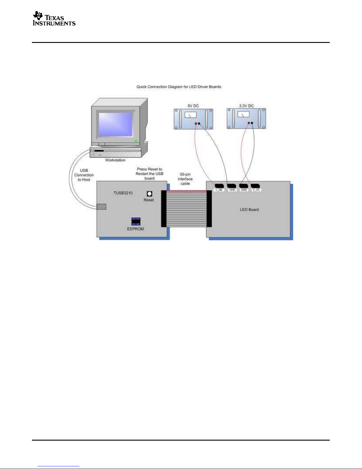
Refer to Figure 1 when setting up the TLC5940EVM hardware.
Attach the 50-pin ribbon cable between the TUSB3210 board and the TLC5940EVM board.
Ensure that the EEPROM on the TUSB3210 board is installed and properly seated.
Attach the 5.5-volt (2-A) power supply to the LED board between J5 (V_GB) and J6 (GND).
TLC5940 EVM2 SLVU139 – September 2005
Page 3
www.ti.com
Introduction
Attach the 3.3-volt (500-mA) power supply to the LED board between J4 (V_CC) and J7 (GND).
Connect the host computer to the TUSB3210 board using the USB cable. If the computer is running, a
message about installing new hardware may be displayed. Follow the on-screen instructions and allow
windows to install the default drivers for this device. Note that the USB board appears to windows as a
generic human interface device (such as a keypad or a mouse), so there is no custom driver to install.
1.3 Input/Output Connector Descriptions
1.3.1 J1 – Interface Connector
J1 provides easy access to all signals necessary to control the TLC5940EVM. This connector is useful for
interfacing the customer controller board to the EVM. Refer to the data sheet for a more detailed
description of each signal’s function. Do not actively drive the same signals on J1 and J3 at the same
time. As shown on the schematic, these signals from J1 are buffered before reaching the TLC5940 ICs.
Figure 1. Hardware Setup
SLVU139 – September 2005 TLC5940 EVM 3
Page 4
www.ti.com
Introduction
Table 1. J1 – Interface Connector
Pin
Number
Pin Symbol Signal Name I/O Function
1 SIN_RED Serial data input red Input Serial data input for the red LED IC. This is also the serial data input
when all three TLC5940 ICs are connected in cascade mode
(serially).
2 SOUT_R Serial data output red Output Serial data output from the red LED IC
3 SIN_GREEN Serial data input green Input Serial data input for the green LED IC
4 SOUT_G Serial data output green Output Serial data output for the green LED IC
5 SIN_BLUE Serial data input blue Input Serial data input for the blue LED IC
6 SOUT_B Serial data output blue Output Serial data output for the blue LED IC. This is also the serial data
output in cascade mode.
7 SCLK Serial data clock Input Serial data input clock
8 XLAT Data latch Input Rising edge latches data from shift register into the device
9 BLANK Output enable Input Output enable for all channels. Outputs are disabled when BLANK is
high.
10 GSCLK GS PWM Clock Input Grayscale clock signal for 12-bit PWM dimming
11 DCPRG DC PRG Mode Input Selects either the internal register or the internal EEPROM when in
DOT correction mode.
12 XDOWN Error signal Output Error flag (LOD and TEF) output. Note: XDOWN signal of all three
devices is tied together.
13 VPRG_IN VPRG Signal Input This signal is buffered and combined with the /22V_EN signal to set
the VPRG voltage on the TLC5940 ICs.
14 /22V_EN 22V Enable Input This is an active low enable signal that turns on the 22V power
supply that is used to program the internal EEPROM on the
TLC5940 ICs.
15 BUF_EN Buffer enable signal Input This is an active low enable signal that turns on the buffer for the
control signals on the EVM.
16 GND Ground Power Signal ground
1.3.2 J2 – Power Connector
This connector supplies power to the EVM. Table 2 shows pin assignments and Table 3 shows the power
requirements of the EVM. Ensure that the input power has the required current capability. The power
inputs to this connector are identical to the power inputs on J4, J5, J6, and J7.
3, 4, 5, 6, 11, 12 GND Power ground
Table 2. J2 – Power Connector
Pin Number Pin Symbol Function
1, 2 V_CC Supplies bias power for the ICs on the EVM board
7, 8 V_GB Supplies power to drive the LEDs. V_GB is connected to the anode of all three colors of each
RGB LED.
9, 10 V_R Not connected
Table 3. EVM Power Requirements
Pin Number Pin Symbol Voltage Range Max Current
1, 2 V_CC 3.3 V ± 0.1 V > 500 mA
7, 8 V_GB 4.0 V – 17 V > 2000 mA
TLC5940 EVM4 SLVU139 – September 2005
Page 5

www.ti.com
1.3.3 J3 – Interface Connector
This connector is used to connect the TLC5940 EVM to the TUSB3210 interface board. The signals are
the same as on connector J1.
Pin Direction
Number (at board)
19 /22V_EN 22V Enable In This is an active low enable signal that turns on the 22V
20 VRPG_IN VPRG Data In This signal is buffered and combined with the /22V_EN signal
21 XDOWN Error signal Out Error flag (LOD and TEF) output. Note: XDOWN of all three
22 DCPRG DC PRG Mode In Selects either the internal register or the internal EEPROM
23 GSCLK GS PWM Clock In Grayscale clock signal for 12-bit PWM dimming
24 BLANK Output enable In Output enable for all channels. Outputs are disabled when
25 XLAT Data latch In Rising edge latches data from shift register into the device
26 SCLK Serial data clock In Serial data input clock
27 SOUT_B Serial data output blue Out Serial data output for the blue LED IC. This is also the serial
28 SIN_BLUE Serial data input blue In Serial data input for the blue LED IC
29 SOUT_G Serial data output green Out Serial data output for the green LED IC
30 SIN_GREEN Serial data input blue In Serial data input for the blue LED IC
31 SOUT_R Serial data output red Out Serial data output for the red LED IC
32 SIN_RED Serial data input red In Serial data input for the red LED IC. This is also the serial
43,44 3.3V 3.3V Bias In This pin is the 3.3V bus from the TUSB3210 interface board.
47, 48, GND Ground Power Signal ground
49, 50
Introduction
Table 4. J3 – Power Connector
Pin Symbol Signal Name Function
power supply that is used to program the internal EEPROM
on the TLC5940 ICs.
to set the VPRG voltage on the TLC5940 ICs.
devices is tied together.
when in DOT correction mode
BLANK is high.
data output in cascade mode
data input when all three TLC5940 ICs are connected in
cascade mode (serially).
It is not connected to the V_CC pins on the PWB. It can be
connected to V_CC on the PWB by inserting a 0- Ω resistor in
R18.
1.4 Jumper Descriptions
1.4.1 JP1, JP2, JP3 – LED Test Current
These jumpers provide an easy place to measure the current flowing through the D0 red, green, and blue
LEDs. To measure the current, through an LED, remove the jumper and connect a current meter across
the jumper pins. Note that no current can flow through the LEDs if the jumpers are removed and a current
meter is not installed.
1.5 Data Input Modes
The TLC5940EVM-106 can be configured to accept data in two different modes: serially or in parallel. The
default configuration is serial mode. The EVM can be reconfigured for parallel data input by modifying
resistors R2, R3, R4, R6, R7, and R8 according to Table 5.
SLVU139 – September 2005 TLC5940 EVM 5
Page 6

www.ti.com
Introduction
Data Input Mode Data Input Pins Data Output Pins 0- Ω Resistors Open Resistors
Serial data input mode (default) SIN_RED SOUT_B R3, R7 R2, R4, R6, R8
Parallel data input mode SIN_RED, SOUT_R, R2, R4, R6, R8 R3, R7
1.5.1 Serial Data Input Mode
The default configuration is a serial data input connection. In this mode, each of the three TLC5940 data
streams is connected serially. Data from the TUSB3210 enters the TLC5940 board on the SIN_RED pin.
This data goes through the on-board buffer and into the SIN pin on the red TLC5940. The data passes
through this IC and through the green TLC5940 before going into the blue TLC5940. Once the data
stream has filled up the internal registers in all three TLC5940 ICs, it is latched into all ICs at the same
time.
1.5.2 Parallel Data Input Mode
When reconfigured for parallel data input, each of the three TLC5940 ICs is driven from a different data
line. Data goes into the EVM on the SIN_RED, SIN_GREEN, and SIN_BLUE inputs at the same time. The
data then goes through the on-board buffer and into the SIN pins of each TLC5940. The software only
operates in serial mode. The user must provide a driver and software to operate in parallel mode.
Table 5. Data Input Mode Jumper Configurations
SIN_GREEN, SOUT_G,
SIN_BLUE SOUT_B
1.6 EVM Operation
1.6.1 Turning on the EVM
After the software is installed and the hardware is connected as described earlier in this document, the
EVM is ready for use. The startup procedure for the EVM is as follows:
1. Connect all hardware.
2. Turn on the 3.3V and 5.5V power supplies
3. Run the LED Frame Designer software
If the USB cable is removed and reinserted while the software is running, or if power is removed from
VCC, the DOT correction data can become corrupted. To correct this problem, either push the RESET
button on the TUSB3210 PWB or click on the PLAY button in the software.
The default state at startup is to program the LED drivers to 100% DOT correction and 100% grayscale
mode. This produces a white light from the LEDs.
1.6.2 Signal Conditioning Buffer
The TLC5940EVM PWB contains a buffer to condition the input signals to the EVM. This buffer,
SN74AVC16244, eliminates any noise on the input signals, generates fast, clean rise and fall times, and
improves the drive capability of the signal. This circuitry is not necessary for operation of the TLC5940 IC.
It was added to the EVM to eliminate problems that could be caused by noisy drive signals in a test setup.
1.6.3 EEPROM Programming Voltage Supply Circuit
The TLC5940 requires 22V on the VPRG pin in order to program the internal EEPROM. This EEPROM
programming voltage supply circuit uses a TPS61040 IC to provide 22V for this purpose. The circuit
remains off until the /22V_EN signal is pulled low.
TLC5940 EVM6 SLVU139 – September 2005
Page 7

www.ti.com
1.6.4 Switching Circuit for VPRG
The VPRG pin on the TLC5940 performs three functions. The TLC5940 is in grayscale mode when VPRG
= GND and in DOT correction mode when VPRG = VCC. When VPRG = 22V, the TLC5940 can program
DOT correction data into its internal nonvolatile EEPROM. The Switching Circuit for VPRG consisting of
Q1, Q2, Q3, D18, and supporting resistors is designed to switch the VPRG pins on each TLC5940
between these three voltages. Table 6 shows the truth table for generating the VPRG voltage.
/22V_EN VPRG_IN DCPRG VPRG Pin on TLC5940 Description
0 1 0 22 V 22V is enabled and applied to VPRG, but the data cannot be
0 1 1 22 V 22V is enabled and applied to VPRG. The EEPROM can now
1 0 1 0 V Grayscale input mode
1 1 1 3.3 V DOT correction input mode
2 Board Layout
This chapter provides the TLC5940EVM-106 board layout.
Board Layout
Table 6. Data Input Mode Jumper Configurations
written to the EEPROM because DCPRG is low.
be programmed.
SLVU139 – September 2005 TLC5940 EVM 7
Page 8

www.ti.com
Board Layout
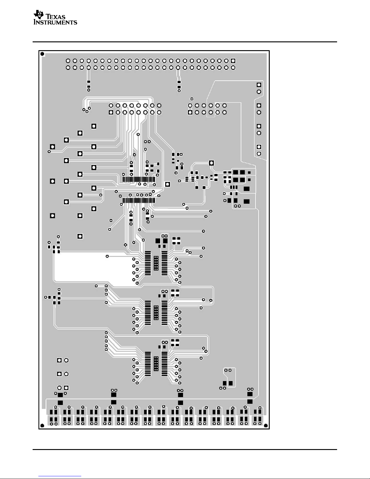
2.1 Layout
TLC5940 EVM8 SLVU139 – September 2005
Figure 2. Assembly Layer
Page 9
www.ti.com
Board Layout
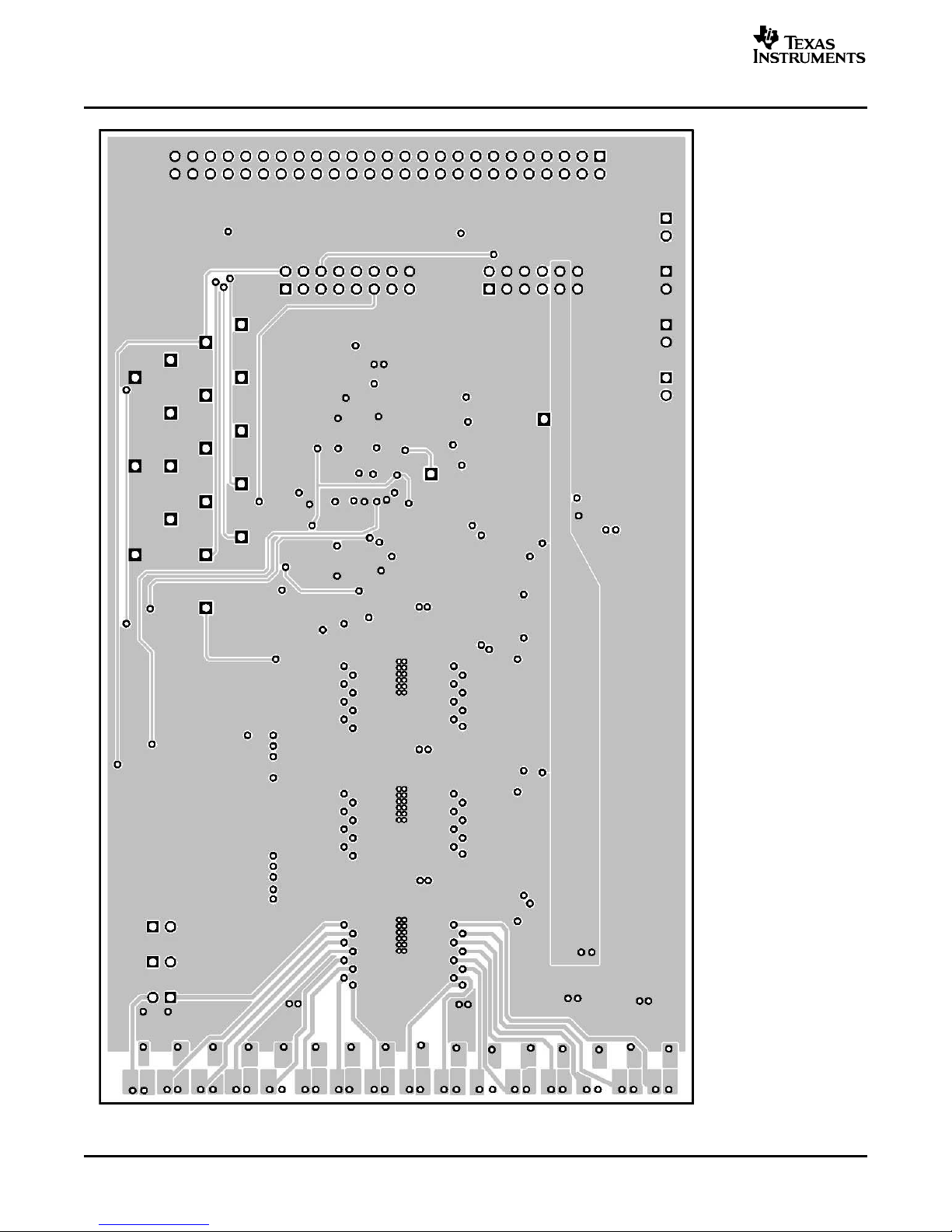
SLVU139 – September 2005 TLC5940 EVM 9
Figure 3. Top Layer Routing
Page 10

www.ti.com
Board Layout
TLC5940 EVM10 SLVU139 – September 2005
Figure 4. Layer 2 Routing
Page 11

www.ti.com
Board Layout
SLVU139 – September 2005 TLC5940 EVM 11
Figure 5. Layer 3 Routing
Page 12
www.ti.com
Board Layout
TLC5940 EVM12 SLVU139 – September 2005
Figure 6. Bottom Layer Routing
Page 13

www.ti.com
3 Related Documentation From Texas Instruments
1. TLC5940 data sheet (SLVS515 )
4 Bill of Materials and Schematic
This chapter provides the TLC5940EVM-106 bill of materials and schematic.
4.1 Bill of Materials
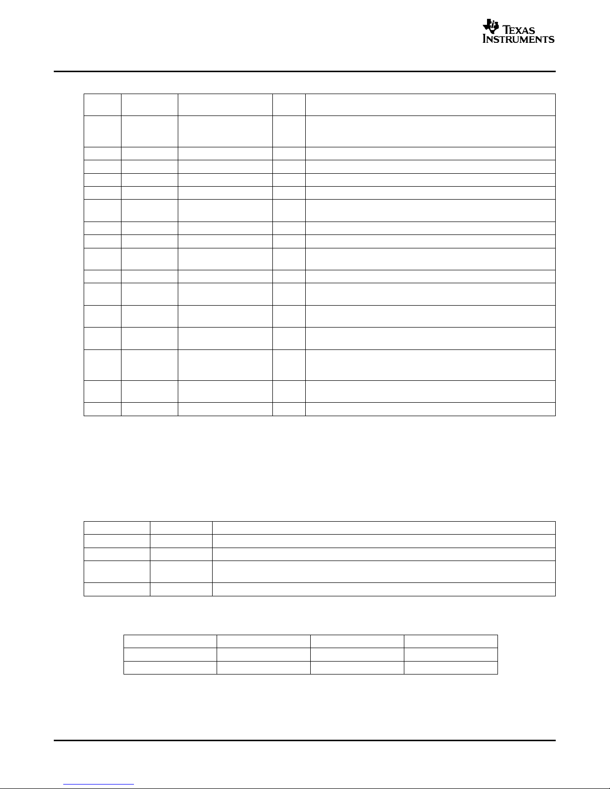
Qty Ref Description Size Part Number MFR
7 C1, C3, C9, Capacitor, ceramic, 0.1 µ F, 25V, X7R, 10% 0603 C1608X7R1H104KT TDK
C11, C12,
C13, C14
1 C15 Capacitor, ceramic, 4.7 µ F, 10V, X5R, 10% 0805 C2012X5R1A475KT muRata
1 C16 Capacitor, ceramic, 22pF, 50V, C0G, 5% 0603 C1608C0G1H220JB TDK
2 C17, C18 Capacitor, ceramic, 1.0 µ F, 50V, X7R, 10% 1206 C3216X7R1H105KT TDK
0 C2, C4, C10 Capacitor, ceramic, xxx µ F, vvV 0603
0 C5 Capacitor, ceramic, xxx µ F, vvV 0805
5 C6, C7, C8, Capacitor, ceramic, 10 µ F, 25V, X5R, 20% 1206 C3216X5R1E106MT TDK
C19, C20
16 D0 - D15 Diode, LED, 20mA, common anode 0.118 x 0.134 Q65110A0697 Osram
1 D16 Diode, LED, red, 20mA, 5mcd 0.114 x 0.049 LN1271RALTRP Panasonic
2 D17, D18 Diode, Schottky, 400mA, 40V SOD323 ZHCS400 Zetex
1 J1 Header, 2x8 pin, 100mil spacing (36 pin strip) 0.100 x 2X8 PTC36DAAN Sullins
1 J2 Header, 2x6 pin, 100mil spacing (36 pin strip) 0.100 x 2X6 PTC36DAAN Sullins
1 J3 Header, low profile, straight 2x25 pin, 100mil 0.100 x 25 x 2 2550-6002UB 3M
spacing
4 J4, J5, J6, Header, 2 pin, 100mil spacing, (36 pin strip) 0.100 x 2 PTC36SAAN Sullins
J7
3 JP1, JP2, Header, 2 pin, 100mil spacing, (36 pin strip) 0.100 x 2 PTC36SAAN Sullins
JP3
1 L1 Inductor, SMT, 10 µ H, 0.55A, 210m Ω 0.205 x 0.160 CDRH3D16-100 Sumida
2 Q1, Q3 MOSFET, Nch, 25V, 0.75A, 66m Ω SOT323 SI1302DL Vishay
1 Q2 MOSFET, Pch, -20V, -1.5A, 180m Ω SC-70 Si1433DH Vishay
3 R1, R5, R9 Resistor, chip, 1.3k Ω , 1/16W, 1% 0603 Std Std
1 R10 Resistor, chip, 121 Ω , 1/16W, 1% 0603 Std Std
3 R11, R12, Resistor, chip, 49.9k Ω , 1/16W, 1% 0603 Std Std
R13
1 R14 Resistor, chip, 2.2M Ω , 1/16W, 1% 0603 Std Std
1 R15 Resistor, chip, 130k Ω , 1/16W, 1% 0603 Std Std
3 R16, R17, Resistor, chip, 249k Ω , 1/16W, 1% 0603 Std Std
R19
0 R2, R4, R6, Resistor, chip, xx Ω , 1/16W, 1% 0603
R8, R18
2 R3, R7 Resistor, chip, 0 Ω , 1/16W, 5% 0603 Std Std
3 TP1, TP2, Test point, black, thru hole color keyed 0.038 5001 Keystone
TP3
17 TP4 - TP20 Test point, red, thru hole color keyed 0.038 5000 Keystone
3 U1, U2, U3 IC, 16 Chan LED driver with dot TSSOP-28 TLC5940PWP TI
correction/grayscale PWM control
Related Documentation From Texas Instruments
Table 7. Bill of Materials
HSMF-A341-A00J1 Agilent
SLVU139 – September 2005 TLC5940 EVM 13
Page 14

www.ti.com
Bill of Materials and Schematic
Table 7. Bill of Materials (continued)
Qty Ref Description Size Part Number MFR
1 U4 IC, 16 Bit buffer driver, 3-state outputs 48P TSSOP SN74AVC16244DGG TI
(DGG)
1 U5 IC, High efficiency boost converter, 250mA, SOT23-5 TPS61040DBV TI
1.8- 6V Vin (DBV)
1 -- PCB, 5.5 In x 3.35 In x 0.062 In HPA106 Any
3 -- Shunt, 100mil, black 0.100 929950-00 3M
TLC5940 EVM14 SLVU139 – September 2005
Page 15

www.ti.com
Bill of Materials and Schematic
4.2 Schematic
SLVU139 – September 2005 TLC5940 EVM 15
Figure 7. TLC5940EVM-106 Schematic
Page 16

www.ti.com
Bill of Materials and Schematic
Figure 8. TLC5940EVM-106 Schematic (Continued)
TLC5940 EVM16 SLVU139 – September 2005
Page 17

FCC Warnings
This equipment is intended for use in a laboratory test environment only. It generates, uses, and can radiate radio frequency
energy and has not been tested for compliance with the limits of computing devices pursuant to subpart J of part 15 of FCC rules,
which are designed to provide reasonable protection against radio frequency interference. Operation of this equipment in other
environments may cause interference with radio communications, in which case the user at his own expense will be required to
take whatever measures may be required to correct this interference.
EVM WARNINGS AND RESTRICTIONS
It is important to operate this EVM within the input voltage ranges specified in Table 3.
Exceeding the specified input range may cause unexpected operation and/or irreversible damage to the EVM. If there are
questions concerning the input range, please contact a TI field representative prior to connecting the input power.
Applying loads outside of the specified output range may result in unintended operation and/or possible permanent damage to the
EVM. Please consult the EVM User's Guide prior to connecting any load to the EVM output. If there is uncertainty as to the load
specification, please contact a TI field representative.
During normal operation, some circuit components may have case temperatures greater than 60 ° C. The EVM is designed to
operate properly with certain components above 60 ° C as long as the input and output ranges are maintained. These components
include but are not limited to linear regulators, switching transistors, pass transistors, and current sense resistors. These types of
devices can be identified using the EVM schematic located in the EVM User's Guide. When placing measurement probes near
these devices during operation, please be aware that these devices may be very warm to the touch.
Mailing Address: Texas Instruments, Post Office Box 655303, Dallas, Texas 75265
Copyright © 2005, Texas Instruments Incorporated
Page 18

IMPORTANT NOTICE
Texas Instruments Incorporated and its subsidiaries (TI) reserve the right to make corrections, modifications,
enhancements, improvements, and other changes to its products and services at any time and to discontinue
any product or service without notice. Customers should obtain the latest relevant information before placing
orders and should verify that such information is current and complete. All products are sold subject to TI’s terms
and conditions of sale supplied at the time of order acknowledgment.
TI warrants performance of its hardware products to the specifications applicable at the time of sale in
accordance with TI’s standard warranty. Testing and other quality control techniques are used to the extent TI
deems necessary to support this warranty . Except where mandated by government requirements, testing of all
parameters of each product is not necessarily performed.
TI assumes no liability for applications assistance or customer product design. Customers are responsible for
their products and applications using TI components. To minimize the risks associated with customer products
and applications, customers should provide adequate design and operating safeguards.
TI does not warrant or represent that any license, either express or implied, is granted under any TI patent right,
copyright, mask work right, or other TI intellectual property right relating to any combination, machine, or process
in which TI products or services are used. Information published by TI regarding third-party products or services
does not constitute a license from TI to use such products or services or a warranty or endorsement thereof.
Use of such information may require a license from a third party under the patents or other intellectual property
of the third party, or a license from TI under the patents or other intellectual property of TI.
Reproduction of information in TI data books or data sheets is permissible only if reproduction is without
alteration and is accompanied by all associated warranties, conditions, limitations, and notices. Reproduction
of this information with alteration is an unfair and deceptive business practice. TI is not responsible or liable for
such altered documentation.
Resale of TI products or services with statements different from or beyond the parameters stated by TI for that
product or service voids all express and any implied warranties for the associated TI product or service and
is an unfair and deceptive business practice. TI is not responsible or liable for any such statements.
Following are URLs where you can obtain information on other Texas Instruments products and application
solutions:
Products Applications
Amplifiers amplifier.ti.com Audio www.ti.com/audio
Data Converters dataconverter.ti.com Automotive www.ti.com/automotive
DSP dsp.ti.com Broadband www.ti.com/broadband
Interface interface.ti.com Digital Control www.ti.com/digitalcontrol
Logic logic.ti.com Military www.ti.com/military
Power Mgmt power.ti.com Optical Networking www.ti.com/opticalnetwork
Microcontrollers microcontroller.ti.com Security www.ti.com/security
Telephony www.ti.com/telephony
Video & Imaging www.ti.com/video
Wireless www.ti.com/wireless
Mailing Address: Texas Instruments
Post Office Box 655303 Dallas, Texas 75265
Copyright 2005, Texas Instruments Incorporated
Page 19

Mouser Electronics
Authorized Distributor
Click to View Pricing, Inventory, Delivery & Lifecycle Information:
Texas Instruments:
TLC5940EVM-106
 Loading...