Texas Instruments TLC27L1IP, TLC27L1IDR, TLC27L1CP, TLC27L1ID, TLC27L1CD Datasheet
...
TLC27L1, TLC27L1A, TLC27L1B
LinCMOS LOW-POWER
OPERATIONAL AMPLIFIERS
SLOS154 – DECEMBER 1995
1
POST OFFICE BOX 655303 • DALLAS, TEXAS 75265
D
Input Offset Voltage Drift...Typically
0.1 µV/Month, Including the First 30 Days
D
Wide Range of Supply Voltages Over
Specified Temperature Range:
0°C to 70°C...3 V to 16 V
–40 °C to 85°C...4 V to 16 V
–55 °C to 125°C...5 V to 16 V
D
Single-Supply Operation
D
Common-Mode Input Voltage Range
Extends Below the Negative Rail (C-Suffix
and I-Suffix Types)
D
Low Noise...68 nV/√Hz Typically at
f = 1 kHz
D
Output Voltage Range includes Negative
Rail
D
High Input Impedance...10
12
Ω Typ
D
ESD-Protection Circuitry
D
Small-Outline Package Option Also
Available in Tape and Reel
D
Designed-In Latch-Up Immunity
description
The TLC27L1 operational amplifier combines a wide range of input offset-voltage grades with low offset-voltage
drift and high input impedance. In addition, the TLC27L1 is a low-bias version of the TLC271 programmable
amplifier. These devices use the Texas Instruments silicon-gate LinCMOS technology, which provides
offset-voltage stability far exceeding the stability available with conventional metal-gate processes.
Three offset-voltage grades are available (C-suffix and I-suffix types), ranging from the low-cost TLC27L1 (10
mV) to the TLC27L1B (2 mV) low-offset version. The extremely high input impedance and low bias currents,
in conjunction with good common-mode rejection and supply voltage rejection, make these devices a good
choice for new state-of-the-art designs as well as for upgrading existing designs.
In general, many features associated with bipolar technology are available in LinCMOS operational amplifiers,
without the power penalties of bipolar technology . General applications such as transducer interfacing, analog
calculations, amplifier blocks, active filters, and signal buffering are all easily designed with the TLC27L1. The
devices also exhibit low-voltage single-supply operation, making them ideally suited for remote and
inaccessible battery-powered applications. The common-mode input-voltage range includes the negative rail.
The device inputs and output are designed to withstand –100-mA surge currents without sustaining latch-up.
The TLC27L1 incorporates internal electrostatic-discharge (ESD) protection circuits that prevent functional
failures at voltages up to 2000 V as tested under MIL-STD-883C, Method 3015.2; however, care should be
exercised in handling these devices as exposure to ESD may result in the degradation of the device parametric
performance.
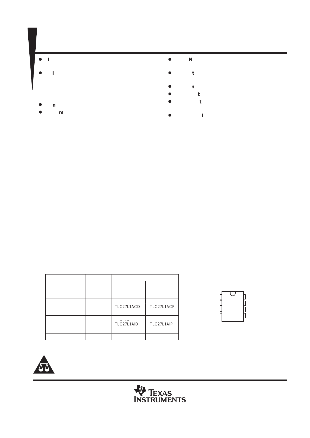
AVAILABLE OPTIONS
PACKAGE
T
A
VIOmax
AT 25°C
SMALL
OUTLINE
(D)
PLASTIC
DIP
(P)
2 mV TLC27L1BCD TLC27L1BCP
0°C to 70°C
2 mV
5 mV
TLC27L1BCD
TLC27L1ACD
TLC27L1BCP
TLC27L1ACP
10 mV TLC27L1CD TLC27L1CP
2 mV TLC27L1BID TLC27L1BIP
–40°C to 85°C
2 mV
5 mV
TLC27L1BID
TLC27L1AID
TLC27L1BIP
TLC27L1AIP
10 mV TLC27L1ID TLC27L1IP
–55°C to 125°C 10 mV TLC27L1MD TLC27L1MP
The D package is available taped and reeled. Add R suffix to the device type
(e.g., TLC27L1BCDR).
Copyright 1995, Texas Instruments Incorporated
PRODUCTION DATA information is current as of publication date.
Products conform to specifications per the terms of Texas Instruments
standard warranty. Production processing does not necessarily include
testing of all parameters.
Please be aware that an important notice concerning availability, standard warranty, and use in critical applications of
Texas Instruments semiconductor products and disclaimers thereto appears at the end of this data sheet.
LinCMOS is a trademark of Texas Instruments Incorporated.
1
2
3
4
8
7
6
5
OFFSET N1
IN –
IN +
GND
V
DD
V
DD
OUT
OFFSET N2
D OR P PACKAGE
(TOP VIEW)
TLC27L1, TLC27L1A, TLC27L1B
LinCMOS LOW-POWER
OPERATIONAL AMPLIFIERS
SLOS154 – DECEMBER 1995
2
POST OFFICE BOX 655303 • DALLAS, TEXAS 75265
description (continued)
The C-suffix devices are characterized for operation from 0°C to 70°C. The I-suffix devices are characterized
for operation from –40°C to 85°C. The M-suffix devices are characterized for operation over the full military
temperature range of –55°C to 125°C.
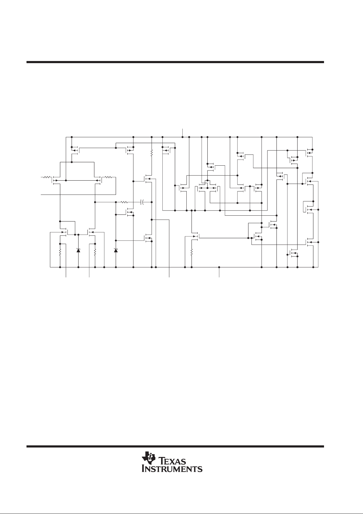
equivalent schematic
P3
P1
R1
IN –
IN +
P2 R2
P4
R6
N5
R5
C1
N3
N2N1
R3
D1
R4
D2
N4
OFFSET
N1
N2
OFFSET
OUT
GND
R7
N6
N10
N7
N9
N13
N12
N11
P12
P11
P10
P7A
P8
P9A
P9B
P7B
P6BP6A
P5
V
DD
TLC27L1, TLC27L1A, TLC27L1B
LinCMOS LOW-POWER
OPERATIONAL AMPLIFIERS
SLOS154 – DECEMBER 1995
3
POST OFFICE BOX 655303 • DALLAS, TEXAS 75265
absolute maximum ratings over operating free-air temperature (unless otherwise noted)
†
Supply voltage, V
DD
(see Note 1) 8 V. . . . . . . . . . . . . . . . . . . . . . . . . . . . . . . . . . . . . . . . . . . . . . . . . . . . . . . . . . . . .
Differential input voltage, V
ID
(see Note 2) ±V
DD
. . . . . . . . . . . . . . . . . . . . . . . . . . . . . . . . . . . . . . . . . . . . . . . . . . .
Input voltage range, V
I
(any input) – 0.3 V to V
DD
. . . . . . . . . . . . . . . . . . . . . . . . . . . . . . . . . . . . . . . . . . . . . . . . . . .
Input current, I
I
±5 mA. . . . . . . . . . . . . . . . . . . . . . . . . . . . . . . . . . . . . . . . . . . . . . . . . . . . . . . . . . . . . . . . . . . . . . . . . .
Output current, I
O
±30 mA. . . . . . . . . . . . . . . . . . . . . . . . . . . . . . . . . . . . . . . . . . . . . . . . . . . . . . . . . . . . . . . . . . . . . . .
Duration of short-circuit current at (or below) 25°C (see Note 3) Unlimited. . . . . . . . . . . . . . . . . . . . . . . . . . . . . .
Continuous total power dissipation See Dissipation Rating Table. . . . . . . . . . . . . . . . . . . . . . . . . . . . . . . . . . . . .
Operating free-air temperature, T
A
: C suffix 0°C to 70°C. . . . . . . . . . . . . . . . . . . . . . . . . . . . . . . . . . . . . . . . . . . .
I suffix –40°C to 85°C. . . . . . . . . . . . . . . . . . . . . . . . . . . . . . . . . . . . . . . . . . .
M suffix –55°C to 125°C. . . . . . . . . . . . . . . . . . . . . . . . . . . . . . . . . . . . . . . . .
Storage temperature range, T
stg
–65°C to 150°C. . . . . . . . . . . . . . . . . . . . . . . . . . . . . . . . . . . . . . . . . . . . . . . . . . .
Case temperature for 60 seconds, T
C
: FK package 260°C. . . . . . . . . . . . . . . . . . . . . . . . . . . . . . . . . . . . . . . . . .
Lead temperature 1,6 mm (1/16 inch) from case for 10 seconds: D or P package 260°C. . . . . . . . . . . . . . . . .
†
Stresses beyond those listed under “absolute maximum ratings” may cause permanent damage to the device. These are stress ratings only, and
functional operation of the device at these or any other conditions beyond those indicated under “recommended operating conditions” is not
implied. Exposure to absolute-maximum-rated conditions for extended periods may affect device reliability.
NOTES: 1. All voltage values, except differential voltages, are with respect to network ground.
2. Differential voltages are at IN+ with respect to IN–.
3. The output may be shorted to either supply. Temperature and/or supply voltages must be limited to ensure that the maximum
dissipation rating is not exceeded (see application section).
DISSIPATION RATING TABLE
PACKAGE
TA ≤ 25°C
POWER RATING
DERATING FACTOR
ABOVE TA = 25°C
TA = 70°C
POWER RATING
TA = 85°C
POWER RATING
TA = 125°C
POWER RATING
D 725 mW 5.8 mW/°C 464 mW 377 mW 145 mW
P 1000 mW 8.0 mW/°C 640 mW 520 mW 200 mW
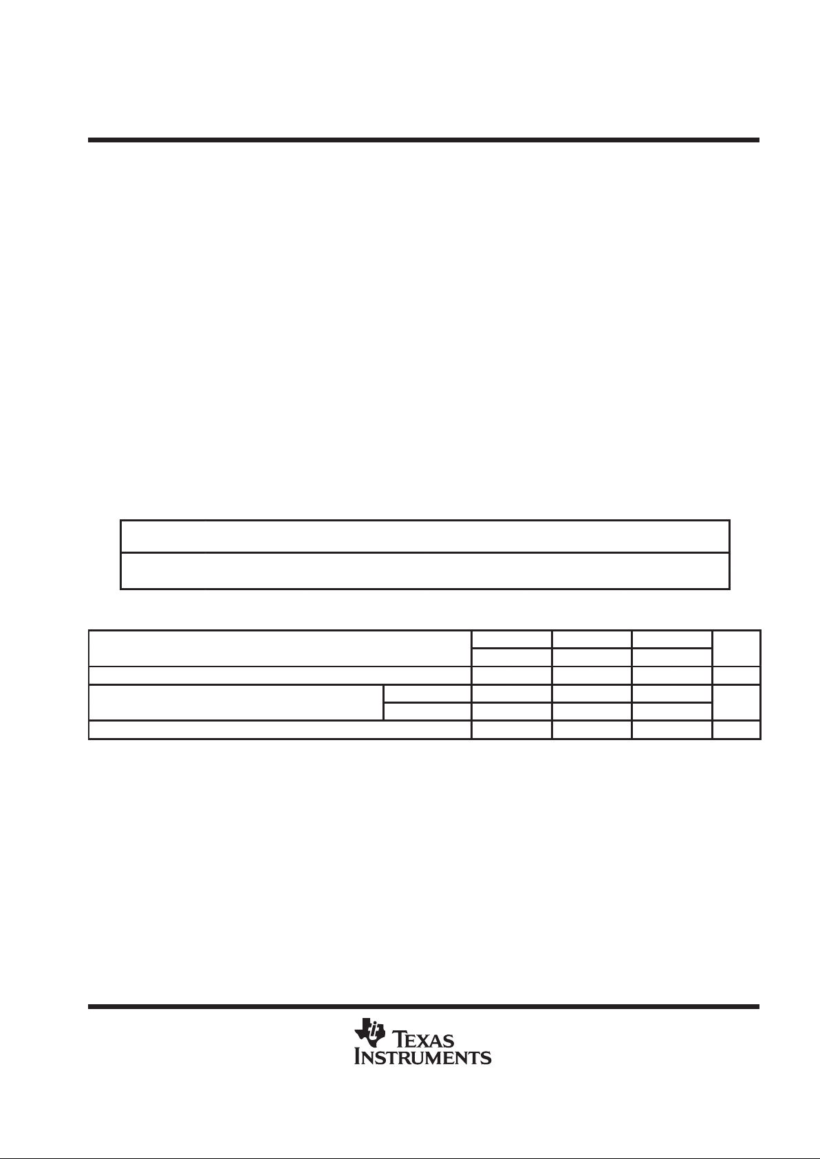
recommended operating conditions
C SUFFIX I SUFFIX M SUFFIX
MIN MAX MIN MAX MIN MAX
UNIT
Supply voltage, V
DD
3 16 4 16 5 16 V
p
VDD = 5 V –0.2 3.5 –0.2 3.5 0 3.5
Common-mode input voltage, V
IC
VDD = 10 V –0.2 8.5 –0.2 8.5 0 8.5
V
Operating free-air temperature, T
A
0 70 –40 85 –55 125 °C
TLC27L1, TLC27L1A, TLC27L1B
LinCMOS LOW-POWER
OPERATIONAL AMPLIFIERS
SLOS154 – DECEMBER 1995
4
POST OFFICE BOX 655303 • DALLAS, TEXAS 75265
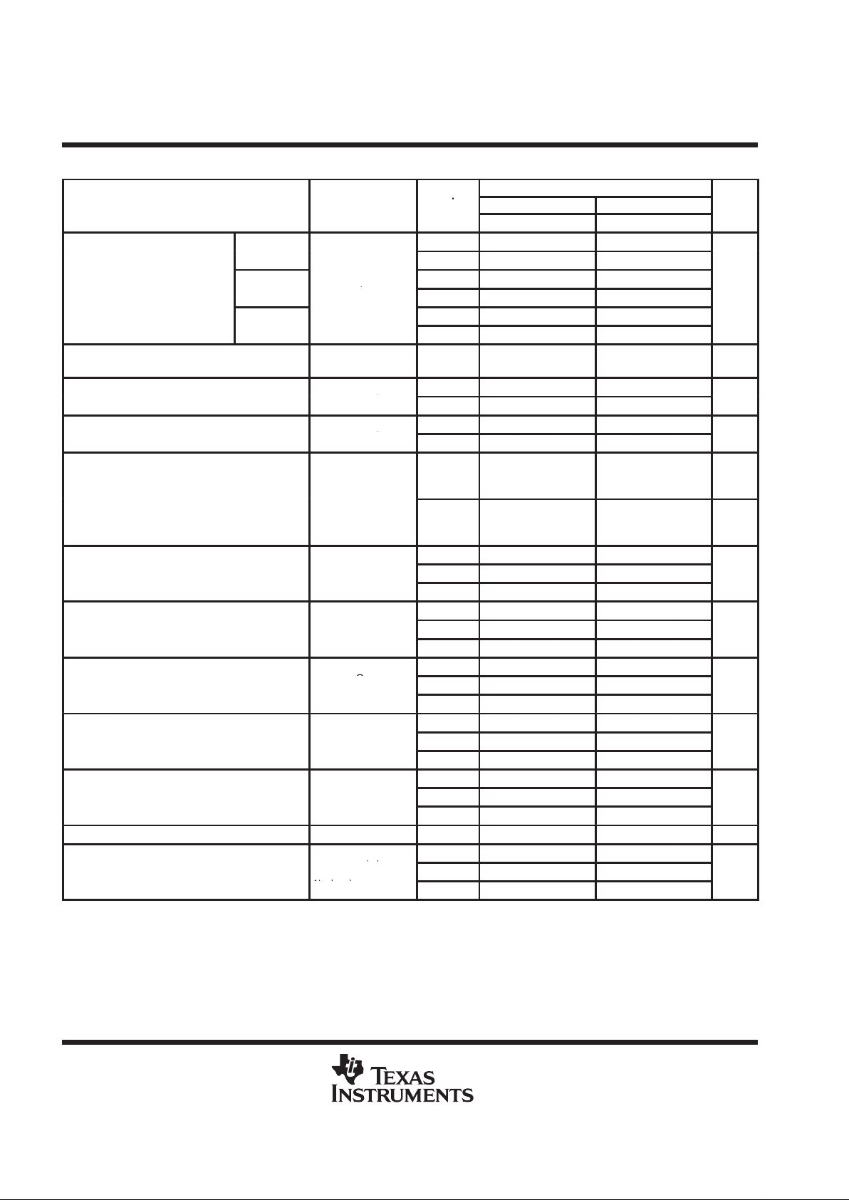
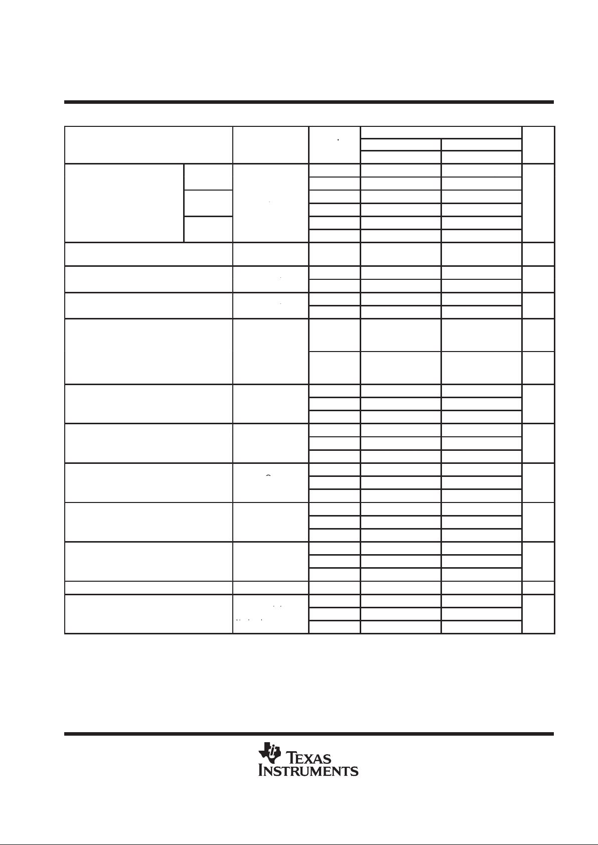
electrical characteristics at specified free-air temperature (unless otherwise noted)
TLC27L1C, TLC27L1AC, TLC27L1BC
PARAMETER
TEST
T
A
†
VDD = 5 V VDD = 10 V
UNIT
CONDITIONS
A
MIN TYP MAX MIN TYP MAX
25°C 1.1 10 1.1 10
TLC27L1C
Full range 12 12
p
V
O
= 1.4 V,
V
= 0 V,
25°C 0.9 5 0.9 5
VIOInput offset voltage
TLC27L1AC
IC
,
RS = 50 Ω,
Full range 6.5 6.5
mV
RI = 1 MΩ
25°C 0.24 2 0.26 2
TLC27L1BC
Full range 3 3
α
VIO
Average temperature coefficient of
input offset voltage
25°C to
70°C
1.1 1 µV/°C
p
V
= V
/2,
25°C 0.1 0.1
p
IIOInput offset current (see Note 4)
ODD
,
VIC = VDD/2
70°C 7 300 8 300
pA
p
V
= V
/2,
25°C 0.6 0.7
p
IIBInput bias current (see Note 4)
ODD
,
VIC = VDD/2
70°C 40 600 50 600
pA
Common-mode input
25°C
–0.2
to
4
–0.3
to
4.2
–0.2
to
9
–0.3
to
9.2
V
V
ICR
voltage range (see Note 5)
Full range
–0.2
to
3.5
–0.2
to
8.5
V
25°C 3.2 4.1 8 8.9
V
OH
High-level output voltage
VID = 100 mV ,
0°C 3 4.1 7.8 8.9
V
RL= 1 MΩ
70°C 3 4.2 7.8 8.9
25°C 0 50 0 50
V
OL
Low-level output voltage
VID = –100 mV ,
0°C 0 50 0 50
mV
I
OL
=
0
70°C 0 50 0 50
25°C 50 520 50 870
A
VD
Large-signal differential
p
RL= 1 MΩ,
0°C 50 700 50 1030
V/mV
voltage am lification
See Note 6
70°C 50 380 50 660
25°C 65 94 65 97
CMRR Common-mode rejection ratio VIC = V
ICR
min
0°C 60 95 60 97
dB
70°C 60 95 60 97
25°C 70 97 70 97
k
SVR
Supply-voltage rejection ratio
VDD = 5 V to 10 V,
0°C 60 97 60 97
dB
(∆VDD/∆VIO)
V
O
= 1.4
V
70°C 60 98 60 98
I
I(SEL)
Input current (BIAS SELECT) V
I(SEL)
= V
DD
25°C 65 95 nA
V
= V
/2
,
25°C 10 17 14 23
I
DD
Supply current
V
O
VDD/2,
VIC = VDD/2,
0°C 12 21 18 33
µA
No load
70°C 8 14 11 20
†
Full range is 0°C to 70°C.
NOTES: 4. The typical values of input bias current and input offset current below 5 pA were determined mathematically.
5. This range also applies to each input individually.
6. At VDD = 5 V, VO = 0.25 V to 2 V; at VDD = 10 V, VO = 1 V to 6 V.
TLC27L1, TLC27L1A, TLC27L1B
LinCMOS LOW-POWER
OPERATIONAL AMPLIFIERS
SLOS154 – DECEMBER 1995
5
POST OFFICE BOX 655303 • DALLAS, TEXAS 75265
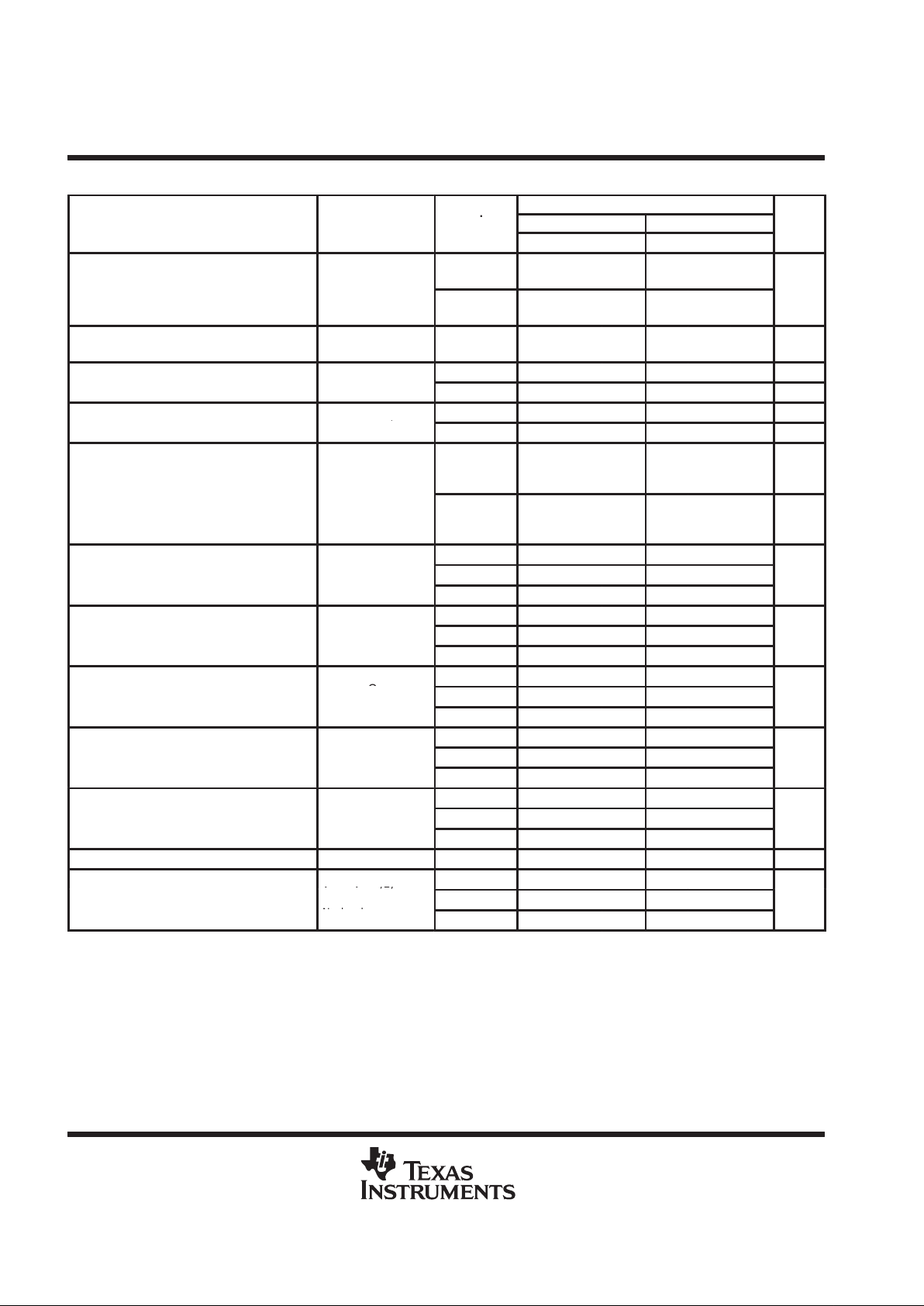
electrical characteristics at specified free-air temperature (unless otherwise noted)
TLC27L1I, TLC27L1AI, TLC27L1BI
PARAMETER
TEST
T
A
†
VDD = 5 V VDD = 10 V
UNIT
CONDITIONS
A
MIN TYP MAX MIN TYP MAX
25°C 1.1 10 1.1 10
TLC27L1I
Full range 13 13
p
V
O
= 1.4 V,
V
= 0 V,
25°C 0.9 5 0.9 5
VIOInput offset voltage
TLC27L1AI
IC
,
RS = 50 Ω,
Full range 7 7
mV
RL = 1 MΩ
25°C 0.24 2 0.26 2
TLC27L1BI
Full range 3.5 3.5
α
VIO
Average temperature coefficient
of input offset voltage
25°C to
85°C
1.1 1 µV/°C
p
V
= V
/2,
25°C 0.1 0.1
p
IIOInput offset current (see Note 4)
ODD
,
VIC = VDD/2
85°C 24 1000 26 1000
pA
p
V
= V
/2,
25°C 0.6 0.7
p
IIBInput bias current (see Note 4)
ODD
,
VIC = VDD/2
85°C 200 2000 220 2000
pA
Common-mode input
25°C
–0.2
to
4
–0.3
to
4.2
–0.2
to
9
–0.3
to
9.2
V
V
ICR
voltage range (see Note 5)
Full range
–0.2
to
3.5
–0.2
to
8.5
V
25°C 3 4.1 8 8.9
V
OH
High-level output voltage
VID = 100 mV ,
–40°C 3 4.1 7.8 8.9
V
RL= 1 MΩ
85°C 3 4.2 7.8 8.9
25°C 0 50 0 50
V
OL
Low-level output voltage
VID = –100 mV,
–40°C 0 50 0 50
mV
I
OL
=
0
85°C 0 50 0 50
25°C 50 520 50 870
A
VD
Large-signal differential
p
RL= 1 MΩ
–40°C 50 900 50 1550
V/mV
voltage am lification
See Note 6
85°C 50 330 50 585
25°C 65 94 65 97
CMRR Common-mode rejection ratio VIC = V
ICR
min
–40°C 60 95 60 97
dB
85°C 60 95 60 98
25°C 70 97 70 97
k
SVR
Supply-voltage rejection ratio
VDD = 5 V to 10 V,
–40°C 60 97 60 97
dB
(∆VDD/∆VIO)
V
O
= 1.4
V
85°C 60 98 60 98
I
I(SEL)
Input current (BIAS SELECT) V
I(SEL)
= V
DD
25°C 65 95 nA
V
= V
/2
,
25°C 10 17 14 23
I
DD
Supply current
V
O
VDD/2,
VIC = VDD/2,
–40°C 16 27 25 43
µA
No load
85°C 17 13 10 18
†
Full range is –40 to 85°C.
NOTES: 4. The typical values of input bias current and input offset current below 5 pA were determined mathematically.
5. This range also applies to each input individually.
6. At VDD = 5 V, VO = 0.25 V to 2 V; at VDD = 10 V, VO = 1 V to 6 V.
TLC27L1, TLC27L1A, TLC27L1B
LinCMOS LOW-POWER
OPERATIONAL AMPLIFIERS
SLOS154 – DECEMBER 1995
6
POST OFFICE BOX 655303 • DALLAS, TEXAS 75265
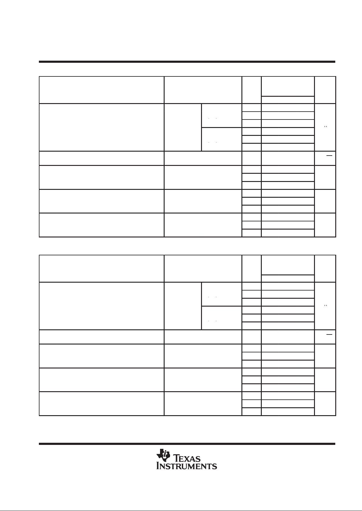
electrical characteristics at specified free-air temperature (unless otherwise noted)
TLC27L1M
PARAMETER
TEST
T
A
†
VDD = 5 V VDD = 10 V
UNIT
CONDITIONS
A
MIN TYP MAX MIN TYP MAX
p
VO = 1.4 V,
VIC = 0 V,
25°C 1.1 10 1.1 10
VIOInput offset voltage
RS = 50 Ω,
RL = 1 MΩ
Full range 12 12
mV
α
VIO
Average temperature coefficient
of input offset voltage
25°C to
125°C
1.4 1.4 µV/°C
p
V
= V
/2,
25°C 0.1 0.1 pA
IIOInput offset current (see Note 4)
ODD
,
VIC = VDD/2
125°C 1.4 15 1.8 15 nA
p
V
= V
/2,
25°C 0.6 0.7 pA
IIBInput bias current (see Note 4)
ODD
,
VIC = VDD/2
125°C 9 35 10 35 nA
Common-mode input
25°C
0
to
4
–0.3
to
4.2
0
to
9
–0.3
to
9.2
V
V
ICR
voltage range (see Note 5)
Full range
0
to
3.5
0
to
8.5
V
25°C 3.2 4.1 8 8.9
V
OH
High-level output voltage
VID = 100 mV ,
–55°C 3 4.1 7.8 8.8
V
RL= 1 MΩ
125°C 3 4.2 7.8 9
25°C 0 50 0 50
V
OL
Low-level output voltage
VID = –100 mV,
–55°C 0 50 0 50
mV
I
OL
=
0
125°C 0 50 0 50
25°C 50 520 50 870
A
VD
Large-signal differential
p
RL= 1 MΩ,
–55°C 25 1000 25 1775
V/mV
voltage am lification
See Note 6
125°C 25 200 25 380
25°C 65 94 65 97
CMRR Common-mode rejection ratio VIC = V
ICR
min
–55°C 60 95 60 97
dB
125°C 60 85 60 91
25°C 70 97 70 97
k
SVR
Supply-voltage rejection ratio
VDD = 5 V to 10 V,
–55°C 60 97 60 97
dB
(∆VDD/∆VIO)
V
O
= 1.4
V
125°C 60 98 60 98
I
I(SEL)
Input current (BIAS SELECT) V
I(SEL)
= V
DD
25°C 65 95 nA
V
= V
/2
,
25°C 10 17 14 23
I
DD
Supply current
V
O
VDD/2,
VIC = VDD/2,
–55°C 17 30 28 48
µA
No load
125°C 7 12 9 15
†
Full range is –55°C to 125°C.
NOTES: 4. The typical values of input bias current and input offset current below 5 pA were determined mathematically.
5. This range also applies to each input individually.
6. At VDD = 5 V, VO = 0.25 V to 2 V; at VDD = 10 V, VO = 1 V to 6 V.
TLC27L1, TLC27L1A, TLC27L1B
LinCMOS LOW-POWER
OPERATIONAL AMPLIFIERS
SLOS154 – DECEMBER 1995
7
POST OFFICE BOX 655303 • DALLAS, TEXAS 75265
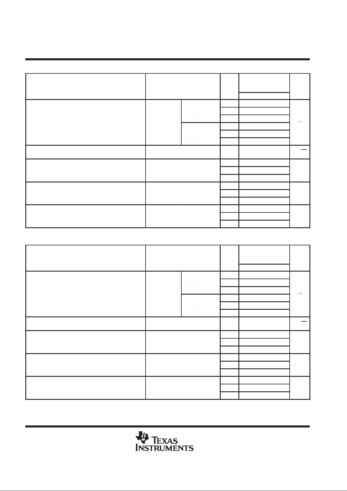
operating characteristics at specified free-air temperature, VDD = 5 V
PARAMETER TEST CONDITIONS T
A
TLC27L1C,
TLC27L1AC,
TLC27L1BC
UNIT
MIN TYP MAX
25°C 0.03
V
I(PP)
= 1 V
0°C 0.04
RL = 1 MΩ,
p
()
70°C 0.03
SR
Slew rate at unity gain
C
L
=
20 pF
,
See Fi
g
ure 33
25°C 0.03
V/µs
See Figure 33
V
I(PP)
= 2.5 V
0°C 0.03
()
70°C 0.02
V
n
Equivalent input noise voltage
f = 1 kHz,
See Figure 34
RS = 20 Ω,
25°C 68
nV/√Hz
25°C 5
B
OM
Maximum output-swing bandwidth
VO = VOH,
CL = 20 pF,
0°C 6
kHz
R
L
= 1 MΩ,
See Figure 33
70°C 4.5
25°C 85
B
1
Unity-gain bandwidth
VI = 10 mV,
CL = 20 pF,
0°C
100
kHz
See Figure 35
70°C 65
25°C 34°
φ
m
Phase margin
V
I
= 10 mV,
p
f
=
B
1
,
0°C 36°
C
L
= 20 F,
See Figure 35
70°C 30°
operating characteristics at specified free-air temperature, VDD = 10 V
PARAMETER TEST CONDITIONS T
A
TLC27L1C,
TLC27L1AC,
TLC27L1BC
UNIT
MIN TYP MAX
25°C 0.05
V
I(PP)
= 1 V
0°C 0.05
RL = 1 MΩ,
p
()
70°C 0.04
SR
Slew rate at unity gain
C
L
= 20 pF,
See Fi
g
ure 33
25°C 0.04
V/µs
See Figure 33
V
I(PP)
= 5.5 V
0°C 0.05
()
70°C 0.04
V
n
Equivalent input noise voltage
f = 1 kHz,
See Figure 34
RS = 20 Ω,
25°C 68
nV/√Hz
25°C 1
B
OM
Maximum output-swing bandwidth
VO = VOH,
CL = 20 pF,
0°C 1.3
kHz
R
L
= 1 MΩ,
See Figure 33
70°C 0.9
25°C 110
B
1
Unity-gain bandwidth
V
I
= 10 mV,
CL = 20 pF,
0°C
125
kHz
See Figure 35
70°C 90
25°C 38°
φ
m
Phase margin
V
I
=
10 mV
,
=
p
f
=
B
1
,
0°C 40°
C
L
= 20 F,
See Figure 35
70°C 34°
TLC27L1, TLC27L1A, TLC27L1B
LinCMOS LOW-POWER
OPERATIONAL AMPLIFIERS
SLOS154 – DECEMBER 1995
8
POST OFFICE BOX 655303 • DALLAS, TEXAS 75265
operating characteristics at specified free-air temperature, VDD = 5 V
PARAMETER TEST CONDITIONS T
A
TLC27L1I,
TLC27L1AI,
TLC27L1BI
UNIT
MIN TYP MAX
25°C 0.03
V
I(PP)
= 1 V
–40°C 0.04
RL = 1 MΩ,
p
()
85°C 0.03
SR
Slew rate at unity gain
C
L
=
20 pF
,
See Fi
g
ure 33
25°C 0.03
V/µs
See Figure 33
V
I(PP)
= 2.5 V
–40°C 0.04
()
85°C 0.02
V
n
Equivalent input noise voltage
f = 1 kHz,
See Figure 34
RS = 20 Ω,
25°C 68
nV/√Hz
25°C 5
B
OM
Maximum output-swing bandwidth
VO = VOH,
CL = 20 pF,
–40°C 7
kHz
R
L
= 1 MΩ,
See Figure 33
85°C 4
25°C 85
B
1
Unity-gain bandwidth
VI = 10 mV,
CL = 20 pF,
–40°C
130
MHz
See Figure 35
85°C 55
25°C 34°
φ
m
Phase margin
V
I
= 10 mV,
p
f
=
B
1
,
–40°C 38°
C
L
= 20 F,
See Figure 35
85°C 28°
operating characteristics at specified free-air temperature, VDD = 10 V
PARAMETER TEST CONDITIONS T
A
TLC27L1C,
TLC27L1AC,
TLC27L1BC
UNIT
MIN TYP MAX
25°C 0.05
V
I(PP)
= 1 V
–40°C 0.06
RL = 1 MΩ,
p
()
85°C 0.03
SR
Slew rate at unity gain
C
L
= 20 pF,
See Fi
g
ure 33
25°C 0.04
V/µs
See Figure 33
V
I(PP)
= 5.5 V
–40°C 0.05
()
85°C 0.03
V
n
Equivalent input noise voltage
f = 1 kHz,
See Figure 34
RS = 20 Ω,
25°C 68
nV/√Hz
25°C 1
B
OM
Maximum output-swing bandwidth
VO = VOH,
CL = 20 pF,
–40°C 1.4
kHz
R
L
= 1 MΩ,
See Figure 33
85°C 0.8
25°C 110
B
1
Unity-gain bandwidth
VI = 10 mV,
CL = 20 pF,
–40°C
155
MHz
See Figure 35
85°C 80
25°C 38°
φ
m
Phase margin
V
I
=
10 mV,l
=
p
f
=
B
1
,
–40°C 42°
C
L
= 20 F,
See Figure 35
85°C 32°
TLC27L1, TLC27L1A, TLC27L1B
LinCMOS LOW-POWER
OPERATIONAL AMPLIFIERS
SLOS154 – DECEMBER 1995
9
POST OFFICE BOX 655303 • DALLAS, TEXAS 75265
operating characteristics at specified free-air temperature, VDD = 5 V
TLC27L1M
PARAMETER
TEST CONDITIONS
T
A
MIN TYP MAX
UNIT
25°C 0.03
V
I(PP)
= 1 V
–55°C 0.04
RL = 1 MΩ,
p
()
125°C 0.02
SR
Slew rate at unity gain
C
L
= 20 pF,
See Fi
g
ure 33
25°C 0.03
V/µs
See Figure 33
V
I(PP)
= 2.5 V
–55°C 0.04
()
125°C 0.02
V
n
Equivalent input noise voltage
f = 1 kHz,
See Figure 34
RS = 20 Ω,
25°C 68
nV/√Hz
25°C 5
B
OM
Maximum output-swing bandwidth
VO = VOH,
CL = 20 pF,
–55°C 8
kHz
R
L
= 1 MΩ,
See Figure 33
125°C 3
25°C 85
B
1
Unity-gain bandwidth
VI = 10 mV,
CL = 20 pF,
–55°C
140
kHz
See Figure 35
125°C 45
25°C 34°
φ
m
Phase margin
V
I
= 10 mV,
p
f
=
B
1
,
–55°C 39°
C
L
= 20 F,
See Figure 35
125°C 25 °
operating characteristics at specified free-air temperature, VDD = 10 V
TLC27L1M
PARAMETER
TEST CONDITIONS
T
A
MIN TYP MAX
UNIT
25°C 0.05
V
I(PP)
= 1 V
–55°C 0.06
RL = 1 MΩ,
p
()
125°C 0.03
SR
Slew rate at unity gain
C
L
= 20 pF,
See Fi
g
ure 33
25°C 0.04
V/µs
See Figure 33
V
I(PP)
= 5.5 V
–55°C 0.06
()
125°C 0.03
V
n
Equivalent input noise voltage
f = 1 kHz,
See Figure 34
RS = 20 Ω,
25°C 68
nV/√Hz
25°C 1
B
OM
Maximum output-swing bandwidth
VO = VOH,
CL = 20 pF,
–55°C 1.5
kHz
R
L
= 1 MΩ,
See Figure 33
125°C 0.7
25°C 110
B
1
Unity-gain bandwidth
VI = 10 mV,
CL = 20 pF,
–55°C
165
kHz
See Figure 35
125°C 70
25°C 38°
φ
m
Phase margin
V
I
=
10 mV
,
p
f
=
B
1
,
–55°C 43°
C
L
= 20 F,
See Figure 35
125°C 29 °
TLC27L1, TLC27L1A, TLC27L1B
LinCMOS LOW-POWER
OPERATIONAL AMPLIFIERS
SLOS154 – DECEMBER 1995
10
POST OFFICE BOX 655303 • DALLAS, TEXAS 75265
TYPICAL CHARACTERISTICS
Table of Graphs
FIGURE
V
IO
Input offset voltage Distribution 1, 2
α
VIO
T emperature coef ficient Distribution 3, 4
vs High-level output current 5, 6
V
OH
High-level output voltage
vs High level out ut current
vs Supply voltage
5, 6
7
OH
gg
yg
vs Free-air temperature 8
-
p
p
vs Common mode in ut voltage
vs Differential input voltage
9, 10
11
VOLLow-level output voltage
g
vs Free-air temperature 12
vs Low-level output current 13, 14
vs Supply voltage 15
A
VD
Large-signal differential voltage amplification
vs Su ly voltage
vs Free-air temperature
15
16
VD
gg g
vs Frequency 27, 28
I
IB
Input bias current vs Free-air temperature 17
I
IO
Input offset current vs Free-air temperature 17
V
I
Maximum input voltage vs Supply voltage 18
pp
vs Supply voltage 19
IDDSupply current
yg
vs Free-air temperature 20
vs Supply voltage 21
SR
Slew rate
yg
vs Free-air temperature 22
Bias-select current vs Supply voltage 23
V
O(PP)
Maximum peak-to-peak output voltage vs Frequency 24
vs Free-air temperature 25
B1Unity-gain bandwidth
vs Supply voltage 26
vs Supply voltage 29
φ
m
Phase margin
vs Su ly voltage
vs Free-air temperature
29
30
φ
m
g
vs Capacitance load 31
V
n
Equivalent input noise voltage vs Frequency 32
Phase shift vs Frequency 27, 28
 Loading...