

Texas Instruments TLC2264IN, TLC2264IDR, TLC2264ID, TLC2264CPWR, TLC2264CPWLE Datasheet
...
TLC226x, TLC226xA
Advanced LinCMOS RAIL-TO-RAIL
OPERATIONAL AMPLIFIERS
SLOS177A – FEBRUARY 1997 – REVISED JULY 1999
1
POST OFFICE BOX 655303 • DALLAS, TEXAS 75265
D
Output Swing includes Both Supply Rails
D
Low Noise . . . 12 nV/√Hz Typ at f = 1 kHz
D
Low Input Bias Current ...1 pA Typ
D
Fully Specified for Both Single-Supply and
Split-Supply Operation
D
Low Power . . . 500 µA Max
D
Common-Mode Input Voltage Range
Includes Negative Rail
D
Low Input Offset Voltage
950 µV Max at TA = 25°C (TLC2262A)
D
Macromodel Included
D
Performance Upgrade for the TS27M2/M4
and TLC27M2/M4
D
Available in Q-Temp Automotive
HighRel Automotive Applications
Configuration Control / Print Support
Qualification to Automotive Standards
description
The TLC2262 and TLC2264 are dual and
quadruple operational amplifiers from Texas
Instruments. Both devices exhibit rail-to-rail
output performance for increased dynamic range
in single- or split-supply applications. The
TLC226x family offers a compromise between the
micropower TLC225x and the ac performance of
the TLC227x. It has low supply current for
battery-powered applications, while still having
adequate ac performance for applications that
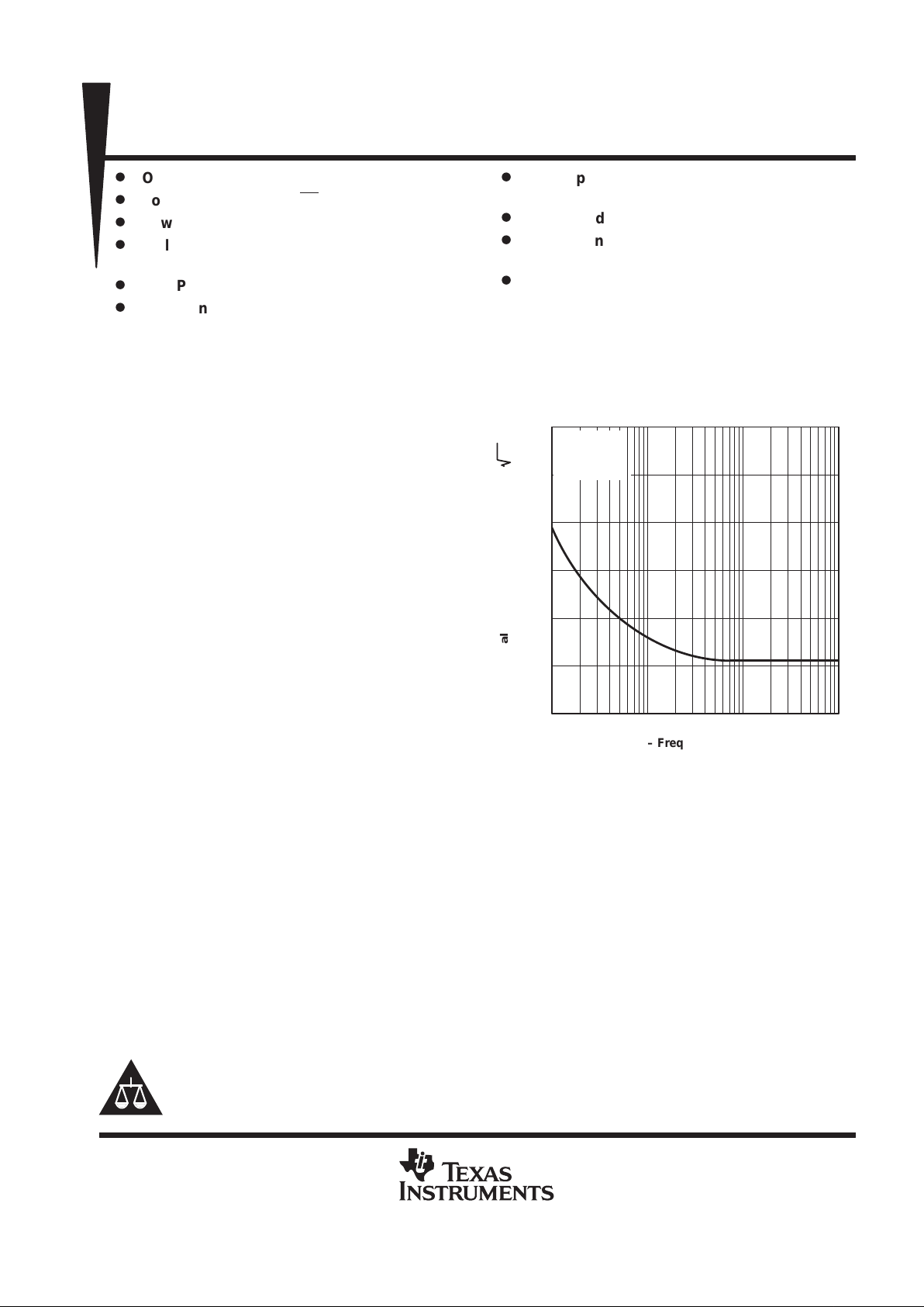
demand it. The noise performance has been
dramatically improved over previous generations
of CMOS amplifiers. Figure 1 depicts the low level
of noise voltage for this CMOS amplifier, which
has only 200 µA (typ) of supply current per
amplifier.
The TLC226x, exhibiting high input impedance
and low noise, are excellent for small-signal
conditioning for high-impedance sources, such as
piezoelectric transducers. Because of the micropower dissipation levels, these devices work well
in hand-held monitoring and remote-sensing
applications. In addition, the rail-to-rail output feature with single or split supplies makes this family a great
choice when interfacing with analog-to-digital converters (ADCs). For precision applications, the TLC226xA
family is available and has a maximum input offset voltage of 950 µV. This family is fully characterized at 5 V
and ±5 V.
The TLC2262/4 also makes great upgrades to the TLC27M2/L4 or TS27M2/L4 in standard designs. They offer
increased output dynamic range, lower noise voltage and lower input offset voltage. This enhanced feature set
allows them to be used in a wider range of applications. For applications that require higher output drive and
wider input voltage range, see the TL V2432 and TL V2442. If your design requires single amplifiers, please see
the TLV2211/21/31 family. These devices are single rail-to-rail operational amplifiers in the SOT-23 package.
Their small size and low power consumption, make them ideal for high density, battery-powered equipment.
Copyright 1999, Texas Instruments Incorporated
PRODUCTION DATA information is current as of publication date.
Products conform to specifications per the terms of Texas Instruments
standard warranty. Production processing does not necessarily include
testing of all parameters.
Please be aware that an important notice concerning availability, standard warranty, and use in critical applications of
Texas Instruments semiconductor products and disclaimers thereto appears at the end of this data sheet.
Advanced LinCMOS is a trademark of Texas Instruments Incorporated.
40
20
10
0
60
30
VN – Equivalent Input Noise Voltage – nv//Hz
50
f – Frequency – Hz
EQUIVALENT INPUT NOISE VOLTAGE
vs
FREQUENCY
10 10
2
10
3
10
4
nV/ Hz
V
n
VDD = 5 V
RS = 20 Ω
TA = 25°C
Figure 1
On products compliant to MIL-PRF-38535, all parameters are tested
unless otherwise noted. On all other products, production
processing does not necessarily include testing of all parameters.
TLC226x, TLC226xA
Advanced LinCMOS RAIL-TO-RAIL
OPERATIONAL AMPLIFIERS
SLOS177A – FEBRUARY 1997 – REVISED JULY 1999
2
POST OFFICE BOX 655303 • DALLAS, TEXAS 75265
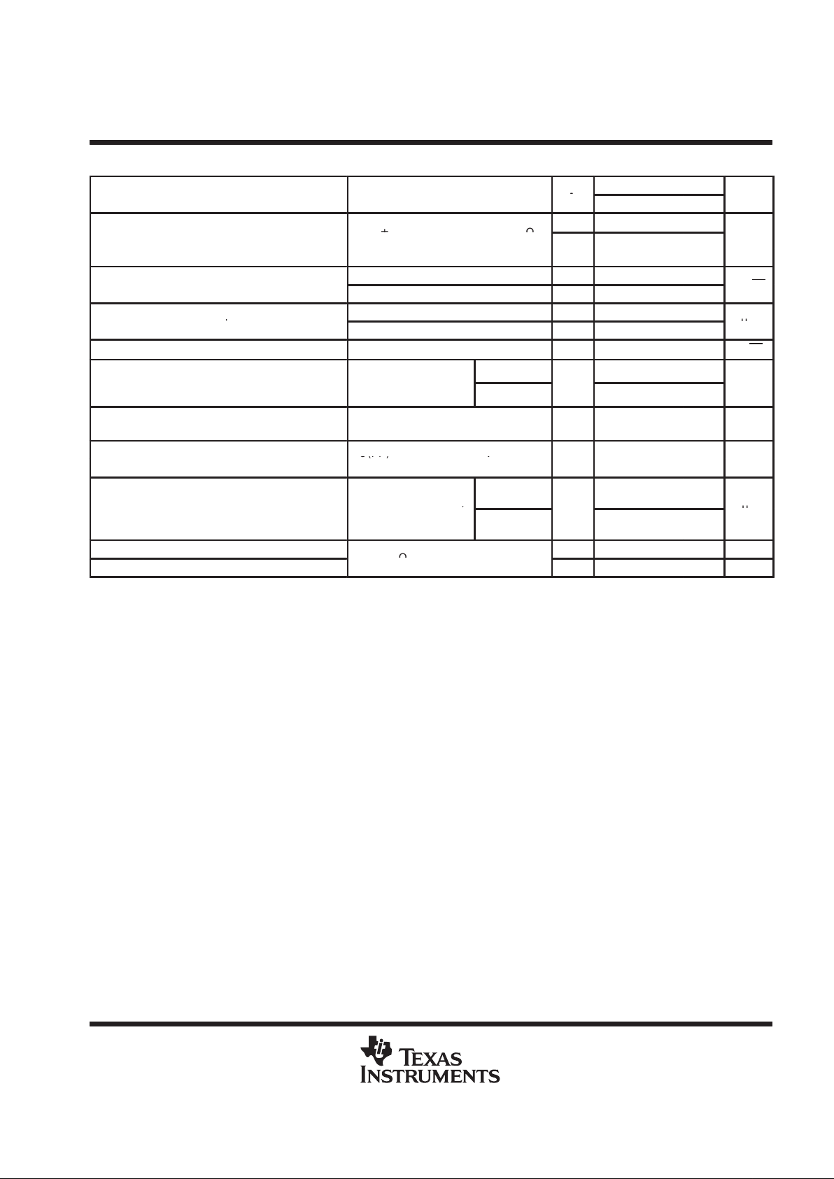
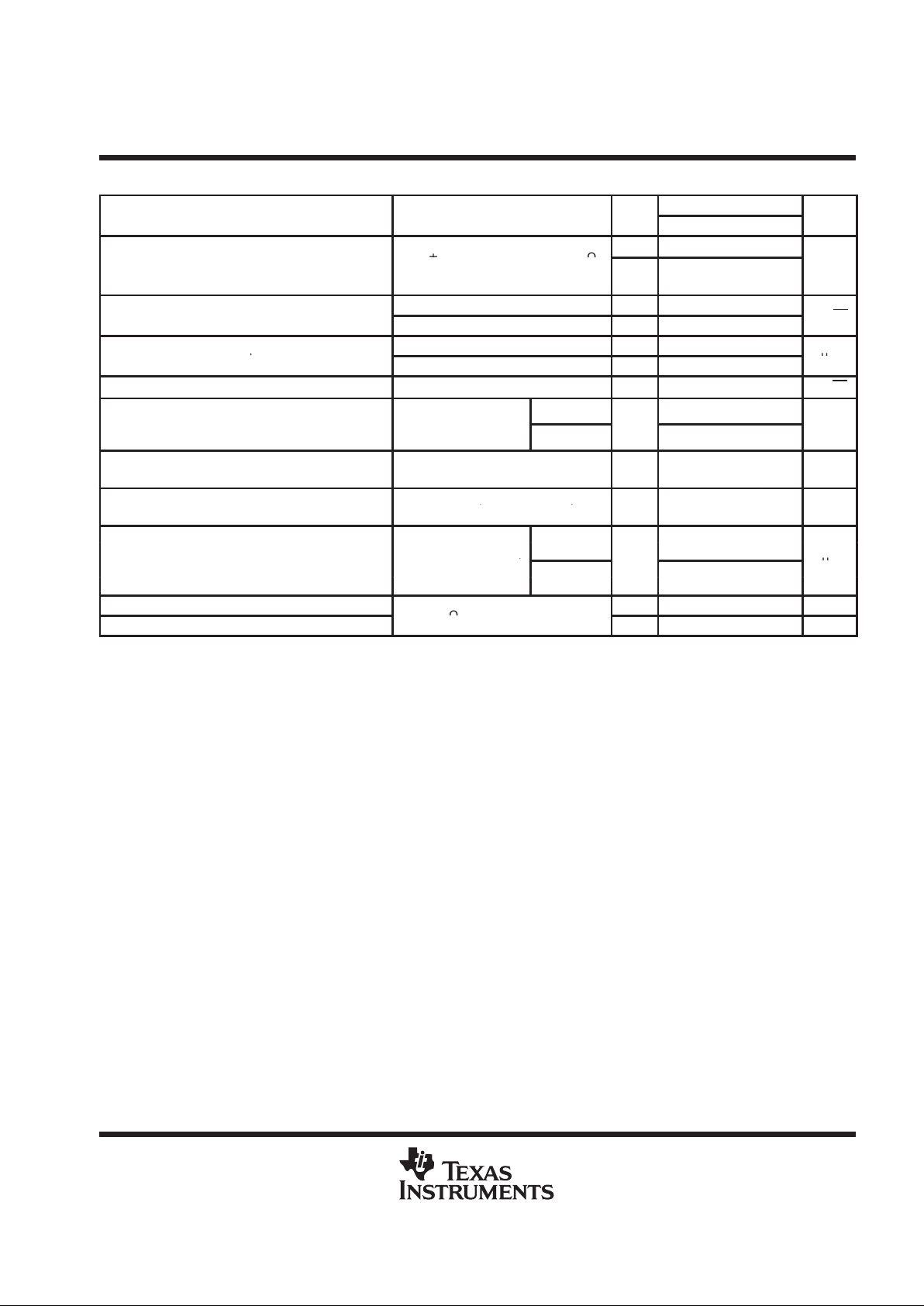
TLC2262 A VAILABLE OPTIONS
PACKAGED DEVICES
T
A
VIOmax
AT 25°C
SMALL
OUTLINE
(D)
CHIP
CARRIER
(FK)
CERAMIC
DIP
(JG)
PLASTIC
DIP
(P)
TSSOP
(PW)
CERAMIC
FLATPACK
(U)
0°C to 70°C 2.5 mV TLC2262CD — — TLC2262CP TLC2262CPWLE —
°
°
950 µV TLC2262AID — — TLC2262AIP TLC2262AIPWLE —
–
40°C to 125°C
µ
2.5 mV TLC2262ID — — TLC2262IP — —
°
°
950 µV TLC2262AQD — — — — —
–
40°C to 125°C
µ
2.5 mV TLC2262QD — — — — —
–55°C to 125°C
950 µV
2.5 mV
—
—
TLC2262AMFK
TLC2262MFK
TLC2262AMJG
TLC2262MJG
—
—
—
—
TLC2262AMU
TLC2262MU
The D packages are available taped and reeled. Add R suffix to device type (e.g., TLC2262CDR). The PW package is available only left-end taped
and reeled. Chips are tested at 25°C.
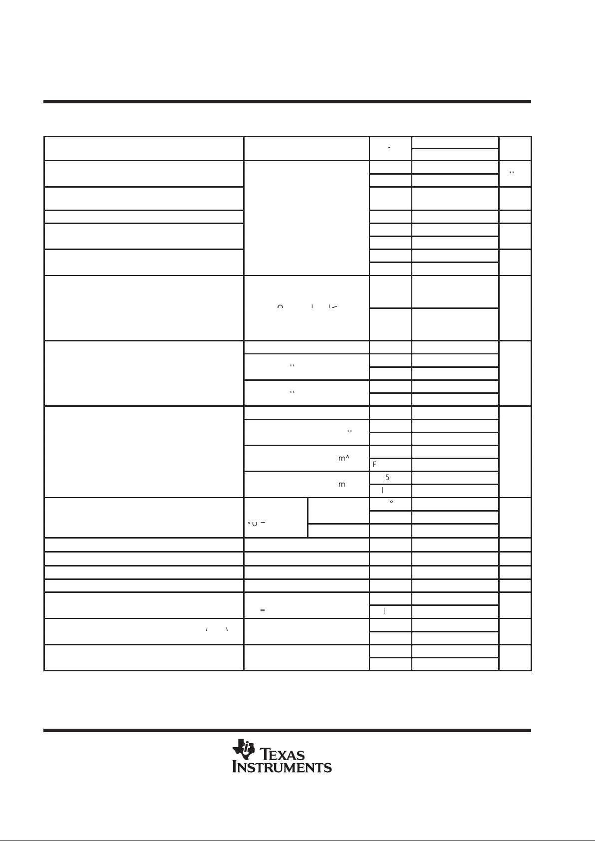
TLC2264 AVAILABLE OPTIONS
PACKAGED DEVICES
T
A
VIOmax
AT 25°C
SMALL
OUTLINE
(D)
CHIP
CARRIER
(FK)
CERAMIC
DIP
(J)
PLASTIC
DIP
(N)
TSSOP
(PW)
CERAMIC
FLATPACK
(W)
0°C to 70°C 2.5 mV TLC2264CD — — TLC2264CN TLC2264CPWLE —
°
°
950 µV TLC2264AID — — TLC2264AIN TLC2264AIPWLE —
–
40°C to 125°C
µ
2.5 mV TLC2264ID — — TLC2264IN — —
°
°
950 µV TLC2264AQD — — — — —
–
40°C to 125°C
µ
2.5 mV TLC2264QD — — — — —
–55°C to 125°C
950 µV
2.5 mV
—
—
TLC2264AMFK
TLC2264MFK
TLC2264AMJ
TLC2264MJ
—
—
—
—
TLC2264AMW
TLC2264MW
The D packages are available taped and reeled. Add R suffix to device type (e.g., TLC2264CDR). The PW package is available only left-end taped
and reeled. Chips are tested at 25°C.
TLC226x, TLC226xA
Advanced LinCMOS RAIL-TO-RAIL
OPERATIONAL AMPLIFIERS
SLOS177A – FEBRUARY 1997 – REVISED JULY 1999
3
POST OFFICE BOX 655303 • DALLAS, TEXAS 75265
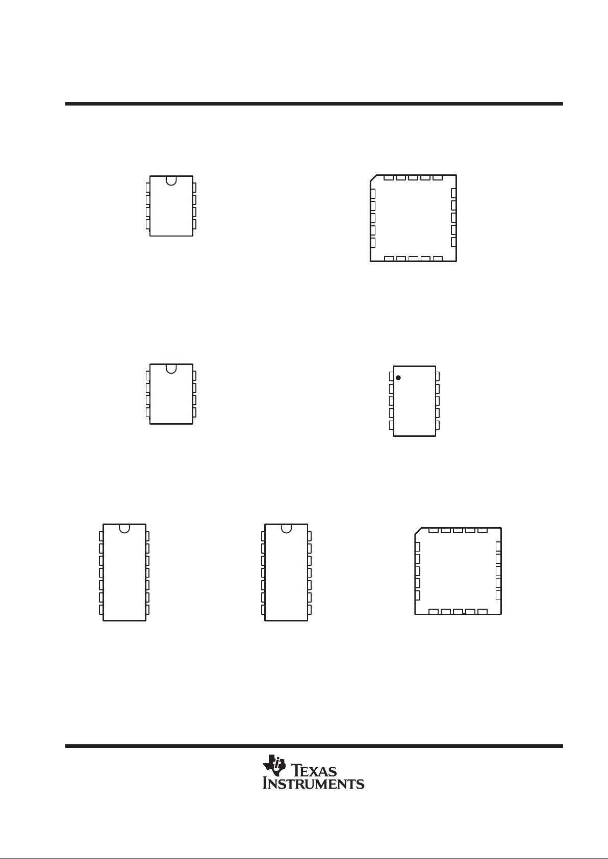
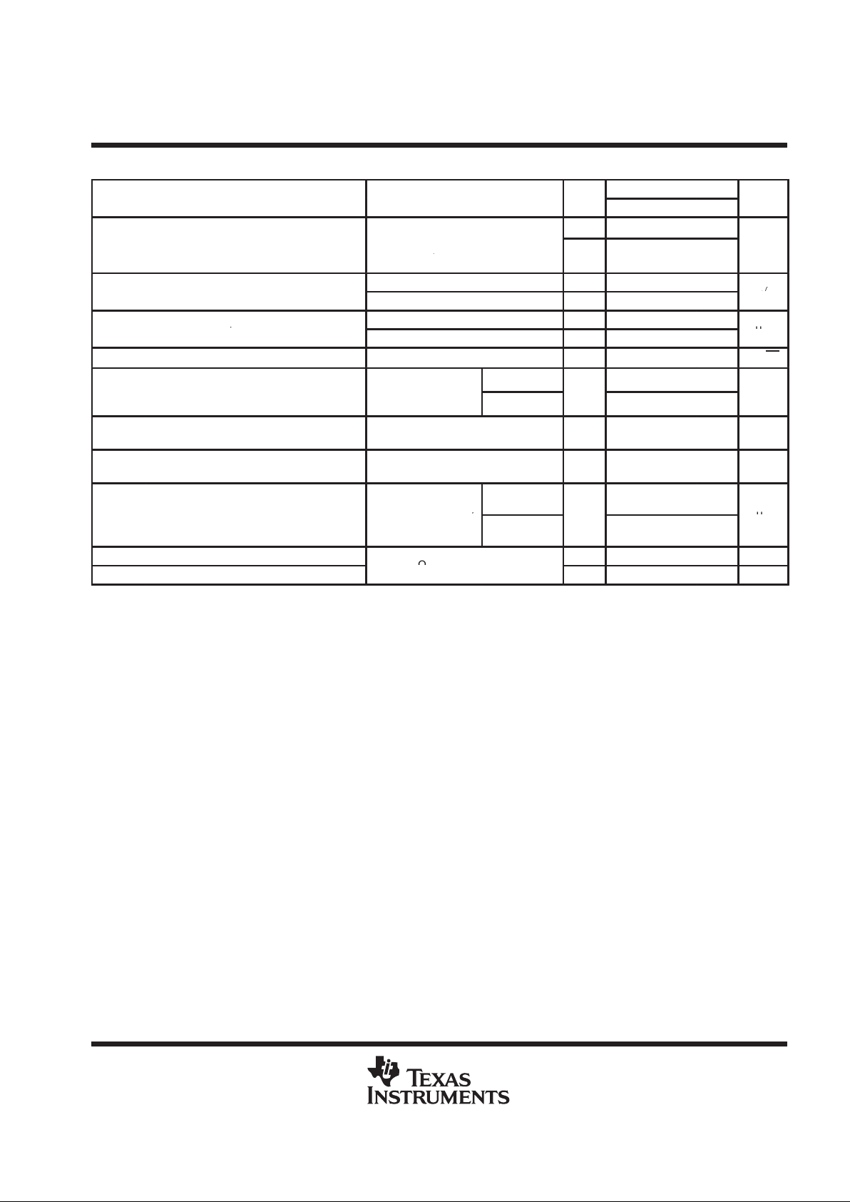
TLC2262M, TLC2262AM . . . JG PACKAGE
(TOP VIEW)
TLC2262C, TLC2262AC
TLC2262I, TLC2262AI
TLC2262Q, TLC2262AQ
D, P, OR PW PACKAGE
(TOP VIEW)
1
2
3
4
8
7
6
5
1OUT
1IN–
1IN+
V
DD–
/GND
V
DD+
2OUT
2IN–
2IN+
NC
V
CC
+
2OUT
2IN –
2IN +
NC
1OUT
1IN –
1IN +
V
CC–
/GND
1
2
3
4
5
10
9
8
7
6
TLC2262M, TLC2262AM ...U PACKAGE
(TOP VIEW)
1
2
3
4
8
7
6
5
1OUT
1IN–
1IN+
V
DD–
/GND
V
DD+
2OUT
2IN–
2IN+
3 2 1 20 19
910111213
4
5
6
7
8
18
17
16
15
14
NC
2OUT
NC
2IN–
NC
NC
1IN–
NC
1IN+
NC
NC
1OUT
NC
2IN+
NC
NC
NC
NC
V
DD+
V
DD–
TLC2262M, TLC2262AM . . . FK PACKAGE
(TOP VIEW)
/GND
1
2
3
4
5
6
7
14
13
12
11
10
9
8
1OUT
1IN–
1IN+
V
DD+
2IN+
2IN–
2OUT
4OUT
4IN–
4IN+
V
DD–
/GND
3IN+
3IN–
3OUT
3 2 1 20 19
910111213
4
5
6
7
8
18
17
16
15
14
4IN+
NC
V
CC–
/GND
NC
3IN+
1IN+
NC
V
CC+
NC
2IN+
1IN –
1OUT
NC
OUT
3IN –
4OUT
4IN –
2IN –
OUT
NC
TLC2264M, TLC2264AM . . . FK PACKAGE
(TOP VIEW)
TLC2264C, TLC2264AC
TLC2264I, TLC2264AI
TLC2264Q, TLC2264AQ
D, N, OR PW PACKAGE
(TOP VIEW)
1
2
3
4
5
6
7
14
13
12
11
10
9
8
1OUT
1IN–
1IN+
V
DD+
2IN+
2IN–
2OUT
4OUT
4IN–
4IN+
V
DD–
/GND
3IN+
3IN–
3OUT
TLC2264M, TLC2264AM ...J OR W PACKAGE
(TOP VIEW)
Template Release Date: 7–11–94
TLC226x, TLC226xA
Advanced LinCMOS
OPERATIONAL AMPLIFIERS
SLOS177A – FEBRUARY 1997 – REVISED JULY 1999
RAIL-TO-RAIL
4
POST OFFICE BOX 655303 DALLAS, TEXAS 75265
•
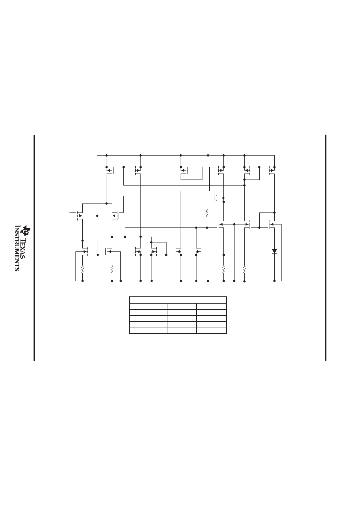
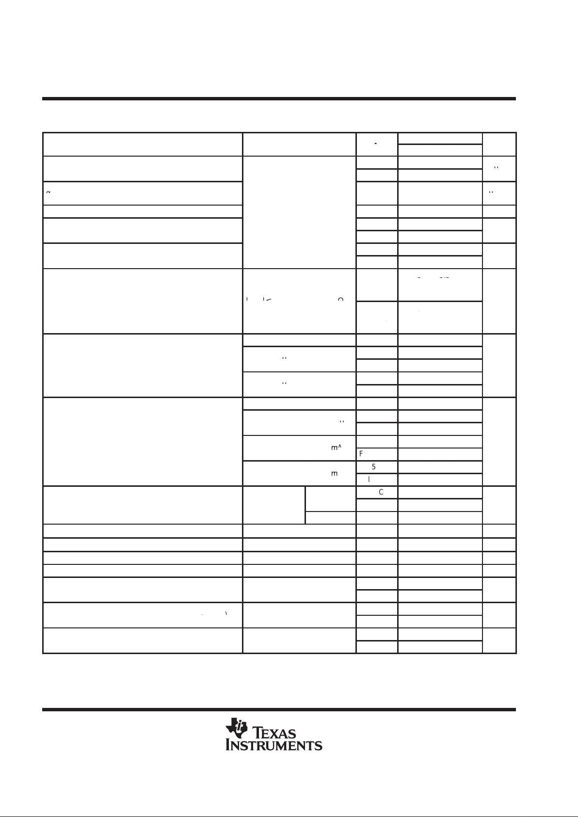
equivalent schematic (each amplifier)
Q3 Q6 Q9 Q12 Q14 Q16
Q2 Q5 Q7 Q8 Q10 Q11
D1
Q17Q15Q13
Q4Q1
R5
C1
V
DD+
IN+
IN–
R3 R4 R1 R2
OUT
V
DD–/ GND
ACTUAL DEVICE COMPONENT COUNT
†
COMPONENT TLC2262 TLC2264
Transistors 38 76
Resistors 28 56
Diodes 9 18
Capacitors 3 6
†
Includes both amplifiers and all ESD, bias, and trim circuitry
TLC226x, TLC226xA
Advanced LinCMOS RAIL-TO-RAIL
OPERATIONAL AMPLIFIERS
SLOS177A – FEBRUARY 1997 – REVISED JULY 1999
5
POST OFFICE BOX 655303 • DALLAS, TEXAS 75265
absolute maximum ratings over operating free-air temperature range (unless otherwise noted)
†
Supply voltage, V
DD+
(see Note 1) 8 V. . . . . . . . . . . . . . . . . . . . . . . . . . . . . . . . . . . . . . . . . . . . . . . . . . . . . . . . . . . .
Supply voltage, V
DD–
(see Note 1) –8 V. . . . . . . . . . . . . . . . . . . . . . . . . . . . . . . . . . . . . . . . . . . . . . . . . . . . . . . . . . .
Differential input voltage, V
ID
(see Note 2) ±16 V. . . . . . . . . . . . . . . . . . . . . . . . . . . . . . . . . . . . . . . . . . . . . . . . . . .
Input voltage, VI (any input, see Note 1) V
DD–
– 0.3 V to V
DD+
. . . . . . . . . . . . . . . . . . . . . . . . . . . . . . . . . . . . . .
Input current, II (each input) ±5 mA. . . . . . . . . . . . . . . . . . . . . . . . . . . . . . . . . . . . . . . . . . . . . . . . . . . . . . . . . . . . . . .
Output current, IO ±50 mA. . . . . . . . . . . . . . . . . . . . . . . . . . . . . . . . . . . . . . . . . . . . . . . . . . . . . . . . . . . . . . . . . . . . . . .
Total current into V
DD+
±50 mA. . . . . . . . . . . . . . . . . . . . . . . . . . . . . . . . . . . . . . . . . . . . . . . . . . . . . . . . . . . . . . . . . .
Total current out of V
DD–
±50 mA. . . . . . . . . . . . . . . . . . . . . . . . . . . . . . . . . . . . . . . . . . . . . . . . . . . . . . . . . . . . . . . .
Duration of short-circuit current at (or below) 25°C (see Note 3) unlimited. . . . . . . . . . . . . . . . . . . . . . . . . . . . . .
Continuous total dissipation See Dissipation Rating Table. . . . . . . . . . . . . . . . . . . . . . . . . . . . . . . . . . . . . . . . . . .
Operating free-air temperature range, TA: C suffix 0°C to 70°C. . . . . . . . . . . . . . . . . . . . . . . . . . . . . . . . . . . . . .
I suffix –40°C to 125°C. . . . . . . . . . . . . . . . . . . . . . . . . . . . . . . . . . . .
Q suffix –40°C to 125°C. . . . . . . . . . . . . . . . . . . . . . . . . . . . . . . . . . .
M suffix –55°C to 125°C. . . . . . . . . . . . . . . . . . . . . . . . . . . . . . . . . .
Storage temperature range, T
stg
–65°C to 150°C. . . . . . . . . . . . . . . . . . . . . . . . . . . . . . . . . . . . . . . . . . . . . . . . . . .
Lead temperature 1,6 mm (1/16 inch) from case for 10 seconds: D, N, P, and PW packages 260°C. . . . . . .
J, JG, U, and W packages 300°C. . . . . . .
†
Stresses beyond those listed under “absolute maximum ratings” may cause permanent damage to the device. These are stress ratings only, and
functional operation of the device at these or any other conditions beyond those indicated under “recommended operating conditions” is not
implied. Exposure to absolute-maximum-rated conditions for extended periods may affect device reliability.
NOTES: 1. All voltage values, except differential voltages, are with respect to the midpoint between V
DD+
and V
DD –
.
2. Differential voltages are at IN+ with respect to IN–. Excessive current flows if input is brought below V
DD–
– 0.3 V.
3. The output may be shorted to either supply. Temperature and/or supply voltages must be limited to ensure that the maximum
dissipation rating is not exceeded.
DISSIPATION RATING TABLE
T
≤ 25°C DERATING FACTOR T
= 70°C T
= 85°C T
= 125°C
PACKAGE
A
POWER RATING ABOVE TA = 25°CAPOWER RATINGAPOWER RATINGAPOWER RATING
D–8 725 mW 5.8 mW/°C 464 mW 377 mW 145 mW
D–14 950 mW 7.6 mW/°C 608 mW 494 mW 190 mW
FK 1375 mW 11.0 mW/°C 880 mW 715 mW 275 mW
J 1375 mW 11.0 mW/°C 880 mW 715 mW 275 mW
JG 1050 mW 8.4 mW/°C 672 mW 546 mW 210 mW
N 1150 mW 9.2 mW/°C 736 mW 598 mW 230 mW
P 1000 mW 8.0 mW/°C 640 mW 520 mW 200 mW
PW–8 525 mW 4.2 mW/°C 336 mW 273 mW 105 mW
PW–14 700 mW 5.6 mW/°C 448 mW 364 mW 140 mW
U 700 mW 5.5 mW/°C 452 mW 370 mW 150 mW
W 700 mW 5.5 mW/°C 452 mW 370 mW 150 mW
recommended operating conditions
C SUFFIX I SUFFIX Q SUFFIX M SUFFIX
MIN MAX MIN MAX MIN MAX MIN MAX
UNIT
Supply voltage, V
DD±
±2.2 ±8 ±2.2 ±8 ±2.2 ±8 ±2.2 ±8 V
Input voltage range, V
I
V
DD–VDD+
–1.5 V
DD–VDD+
–1.5 V
DD–VDD+
–1.5 V
DD–VDD+
–1.5 V
Common-mode input voltage, V
IC
V
DD–VDD+
–1.5 V
DD–VDD+
–1.5 V
DD–VDD+
–1.5 V
DD–VDD+
–1.5 V
Operating free-air temperature, T
A
0 70 –40 125 –40 125 –55 125 °C
TLC226x, TLC226xA
Advanced LinCMOS RAIL-TO-RAIL
OPERATIONAL AMPLIFIERS
SLOS177A – FEBRUARY 1997 – REVISED JULY 1999
6
POST OFFICE BOX 655303 • DALLAS, TEXAS 75265
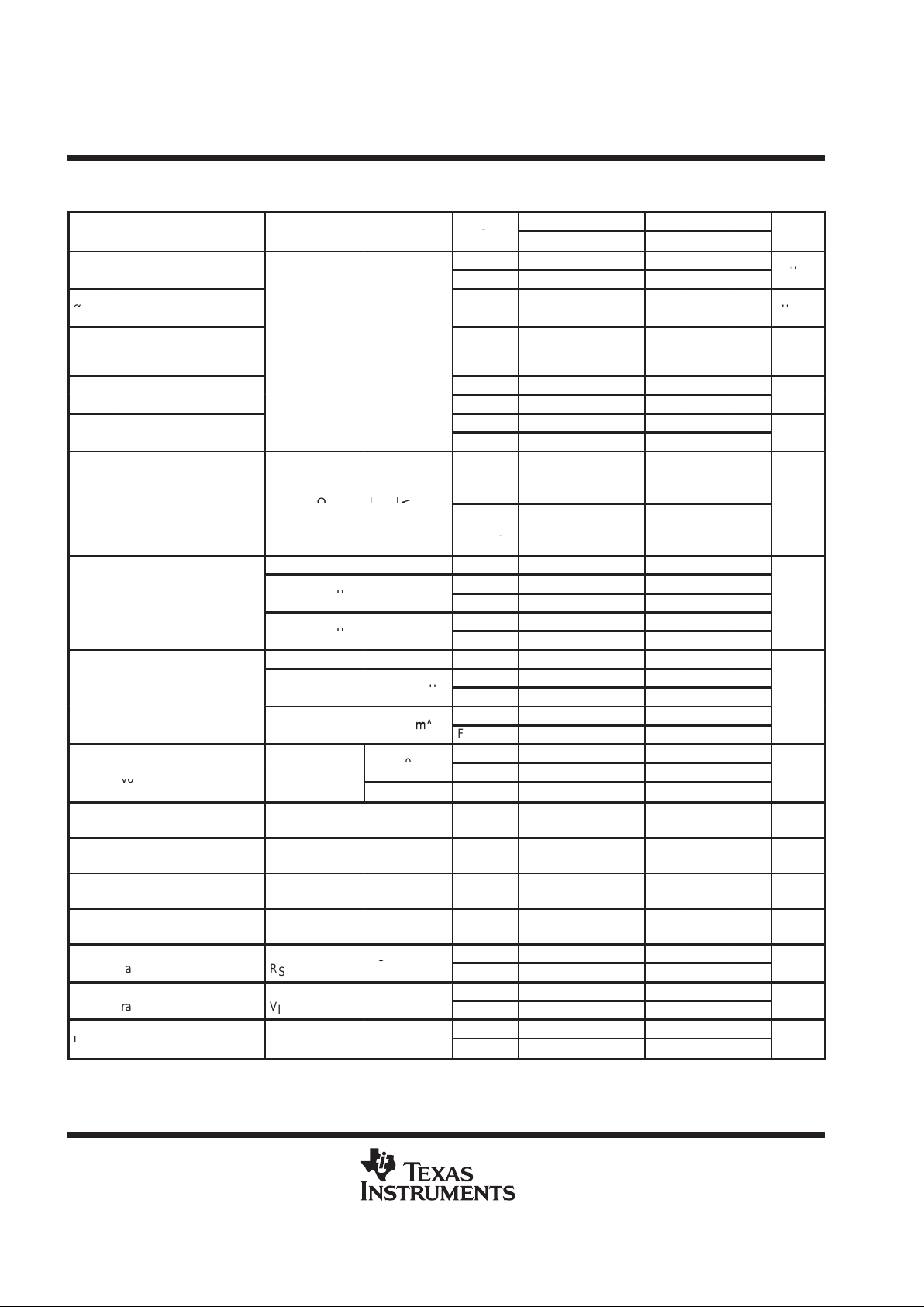
TLC2262C electrical characteristics at specified free-air temperature, VDD = 5 V (unless otherwise
noted)
TLC2262C
PARAMETER
TEST CONDITIONS
T
A
†
MIN TYP MAX
UNIT
p
25°C 300 2500
VIOInput offset voltage
Full range 3000
µ
V
α
VIO
Temperature coefficient of input offset voltage
25°C
to 70°C
2 µV/°C
Input offset voltage long-term drift
(see Note 4)
VIC = 0,
VO = 0,
VDD± = ±2.5 V,
RS = 50 Ω
25°C
0.003 µV/mo
p
O
S
25°C 0.5
p
IIOInput offset current
Full range 100
pA
p
25°C 1
p
IIBInput bias current
Full range 100
pA
p
25°C
0
to
4
–0.3
to
4.2
V
ICR
Common-mode input voltage range
R
S
= 50 Ω,
|V
IO
|
≤ 5 mV
Full range
0
to
3.5
V
IOH = –20 µA 25°C 4.99
25°C 4.85 4.94
V
OH
High-level output voltage
I
OH
= –
100 µA
Full range 4.82
V
25°C 4.70 4.85
I
OH
= –
400 µA
Full range 4.60
VIC = 2.5 V, IOL = 50 µA 25°C 0.01
25°C 0.09 0.15
V
IC
= 2.5 V,
I
OL
=
500 µA
Full range 0.15
V
OL
Low-level output voltage
25°C 0.2 0.3
V
V
IC
=
2.5 V
,
I
OL
=
1 m
A
Full range 0.3
25°C 0.7 1
V
IC
=
2.5 V
,
I
OL
=
4 m
A
Full range 1.2
25°C 80 170
A
VD
Large-signal differential voltage amplification
VIC = 2.5 V,
R
L
= 50
kΩ
‡
Full range 55
V/mV
VD
gg g
V
O
= 1 V to 4
V
RL = 1 MΩ
‡
25°C 550
r
i(d)
Differential input resistance 25°C
10
12
Ω
r
i(c)
Common-mode input resistance 25°C
10
12
Ω
c
i(c)
Common-mode input capacitance f = 10 kHz, P package 25°C 8 pF
z
o
Closed-loop output impedance f = 100 kHz, AV = 10 25°C 240 Ω
V
= 0 to 2.7 V, V
= 2.5 V,
25°C 70 83
CMRR
Common-mode rejection ratio
IC
,
O
,
RS = 50 Ω
Full range 70
dB
pp
V
= 4.4 V to 16 V,
25°C 80 95
k
SVR
Suppl
y-v
oltage rejection ratio (∆VDD/∆VIO)
DD
,
VIC = VDD/2, No load
Full range 80
dB
pp
25°C 400 500
IDDSupply current
V
O
= 2.5 V,
No load
Full range 500
µ
A
†
Full range is 0°C to 70°C.
‡
Referenced to 2.5 V
NOTE 4: Typical values are based on the input offset voltage shift observed through 500 hours of operating life test at TA = 150°C extrapolated
to TA = 25°C using the Arrhenius equation and assuming an activation energy of 0.96 eV .
TLC226x, TLC226xA
Advanced LinCMOS RAIL-TO-RAIL
OPERATIONAL AMPLIFIERS
SLOS177A – FEBRUARY 1997 – REVISED JULY 1999
7
POST OFFICE BOX 655303 • DALLAS, TEXAS 75265
TLC2262C operating characteristics at specified free-air temperature, VDD = 5 V
TLC2262C
PARAMETER
TEST CONDITIONS
T
A
†
MIN TYP MAX
UNIT
V
= 1.5 V to 3.5 V, R
= 50 kه,
25°C 0.35 0.55
SR
Slew rate at unity gain
O
,
CL = 100 pF
‡
L
,
Full range 0.3
V/µs
p
f = 10 Hz 25°C 40
VnEquivalent input noise voltage
f = 1 kHz 25°C 12
n
V/√H
z
Peak-to-peak equivalent input noise
f = 0.1 Hz to 1 Hz 25°C 0.7
V
N(PP)
q
voltage
f = 0.1 Hz to 10 Hz
25°C 1.3
µ
V
I
n
Equivalent input noise current 25°C 0.6
fA√Hz
p
VO = 0.5 V to 2.5 V,
AV = 1
°
0.017%
THD
+
N
Total harmonic distortion plus noise
f
= 20 kHz,
RL = 50 kΩ
‡
AV = 10
25°C
0.03%
Gain-bandwidth product
f = 10 kHz,
CL = 100 pF
‡
RL = 50 kه,
25°C 0.71 MHz
B
OM
Maximum output-swing bandwidth
V
O(PP)
= 2 V,
RL = 50 kه,
AV = 1,
CL = 100 pF
‡
25°C 185 kHz
=–
A
V
= 1,
Step = 0.5 V to 2.5 V ,
To 0.1%°6.4
tsSettling time
,
RL = 50 kه,
25°Cµs
L
CL = 100 pF
‡
To 0.01%
14.1
φ
m
Phase margin at unity gain
p
25°C 56°
Gain margin
R
L
= 50
kΩ
‡
,
C
L
=
100 pF
‡
25°C 11 dB
†
Full range is 0°C to 70°C.
‡
Referenced to 2.5 V
TLC226x, TLC226xA
Advanced LinCMOS RAIL-TO-RAIL
OPERATIONAL AMPLIFIERS
SLOS177A – FEBRUARY 1997 – REVISED JULY 1999
8
POST OFFICE BOX 655303 • DALLAS, TEXAS 75265
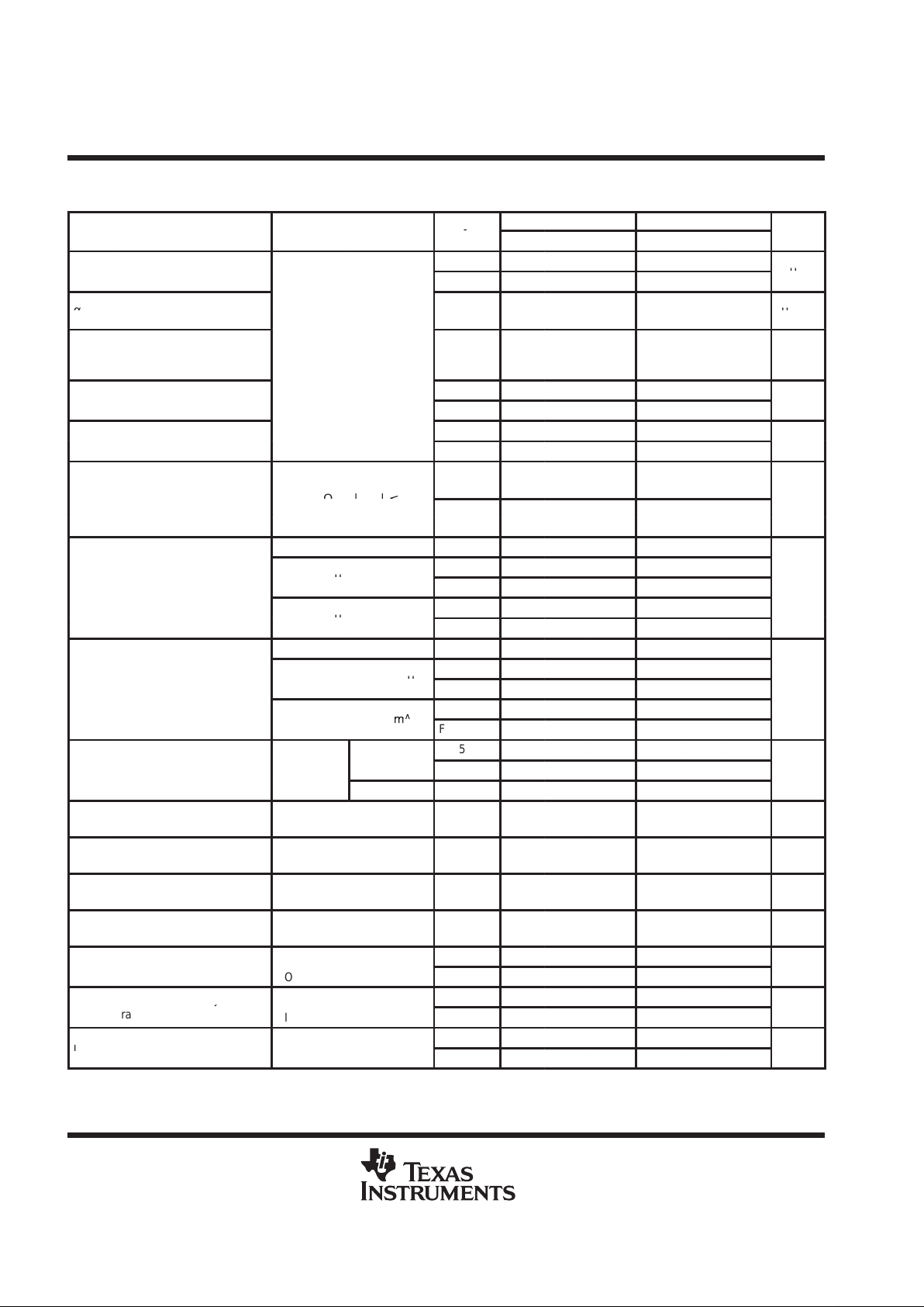
TLC2262C electrical characteristics at specified free-air temperature, V
DD±
= ±5 V (unless
otherwise specified)
TLC2262C
PARAMETER
TEST CONDITIONS
T
A
†
MIN TYP MAX
UNIT
p
25°C 300 2500
VIOInput offset voltage
Full range 3000
µ
V
p
p
25°C
°
α
VIO
Temperature coefficient of input offset voltage
to 70°C
2µV/°C
Input offset voltage long-term drift (see Note 4)
VIC = 0,
VO = 0,
25°C
0.003 µV/mo
p
R
S
= 50
Ω
25°C 0.5
p
IIOInput offset current
Full range 100
pA
p
25°C 1
p
IIBInput bias current
Full range 100
pA
–5 –5.3
25°C
5to5.3
to
p
4 4.2
V
ICR
Common-mode input voltage range
|V
IO
| ≤5 mV,
R
S
= 50
Ω
–5
V
Full range
5
to
g
3.5
IO = –20 µA 25°C 4.99
25°C 4.85 4.94
V
OM+
Maximum positive peak output voltage
I
O
= –
100 µA
Full range 4.82
V
25°C 4.7 4.85
I
O
= –
400 µA
Full range 4.6
VIC = 0, IO = 50 µA 25°C –4.99
25°C –4.85 –4.91
V
IC
= 0,
I
O
=
500 µA
Full range –4.85
V
OM–
Maximum negative peak output voltage
25°C –4.7 –4.8
V
V
IC
= 0,
I
O
= 1
m
A
Full range –4.7
25°C –4 –4.3
V
IC
= 0,
I
O
= 4
m
A
Full range –3.8
25°C 80 200
A
VD
Large-signal differential voltage amplification VO = ±4 V
R
L
=
50 kΩ
Full range 55
V/mV
RL = 1 MΩ 25°C 1000
r
i(d)
Differential input resistance 25°C
10
12
Ω
r
i(c)
Common-mode input resistance 25°C
10
12
Ω
c
i(c)
Common-mode input capacitance f = 10 kHz, P package 25°C 8 pF
z
o
Closed-loop output impedance f = 100 kHz, AV = 10 25°C 220
Ω
V
= –5 V to 2.7 V,
25°C 75 88
CMRR
Common-mode rejection ratio
IC
,
VO = 0 V, RS = 50 Ω
Full range 75
dB
pp
V
= 2.2 V to ±8 V,
25°C 80 95
k
SVR
Suppl
y-v
oltage rejection ratio (∆V
DD±
/∆VIO)
DD±
,
VIC = 0, No load
Full range 80
dB
pp
25°C 425 500
IDDSupply current
V
O
= 0 V,
No load
Full range 500
µ
A
†
Full range is 0°C to 70°C.
NOTE 4: Typical values are based on the input offset voltage shift observed through 500 hours of operating life test at TA = 150°C extrapolated
to TA = 25°C using the Arrhenius equation and assuming an activation energy of 0.96 eV .
TLC226x, TLC226xA
Advanced LinCMOS RAIL-TO-RAIL
OPERATIONAL AMPLIFIERS
SLOS177A – FEBRUARY 1997 – REVISED JULY 1999
9
POST OFFICE BOX 655303 • DALLAS, TEXAS 75265
TLC2262C operating characteristics at specified free-air temperature, V
DD±
= ±5 V
TLC2262C
PARAMETER
TEST CONDITIONS
T
A
†
MIN TYP MAX
UNIT
25°C 0.35 0.55
SR Slew rate at unity gain
V
O
=
±1.9 V
,
=
p
R
L
=
50 kΩ
,
Full
V/µs
C
L
=
100 F
range
0.3
p
f = 10 Hz 25°C 43
VnEquivalent input noise voltage
f = 1 kHz 25°C 12
n
V/√H
z
Peak-to-peak equivalent input noise
f = 0.1 Hz to 1 Hz 25°C 0.8
V
N(PP)
q
voltage
f = 0.1 Hz to 10 Hz
25°C 1.3
µ
V
I
n
Equivalent input noise current 25°C 0.6
fA√Hz
p
VO = ±2.3 V,
AV = 1
°
0.014%
THD
+
N
Total harmonic distortion pulse duration
f
= 20 kHz,
RL = 50 kΩ
AV = 10
25°C
0.024%
p
f = 10 kHz, R
= 50 kΩ,
°
Gain-bandwidth product
,
CL = 100 pF
L
,
25°C
0.73
MH
z
p
V
O(PP
)
= 4.6 V, AV = 1,
°
BOMMaximum output-swing bandwidth
O(PP)
RL = 50 kΩ,
V
CL = 100 pF
25°C85kH
z
=–
A
V
= 1,
Step = –2.3 V to 2.3 V,
To 0.1%
°
7.1
tsSettling time
,
RL = 50 kΩ,
25°Cµs
L
CL = 100 pF
To 0.01%
16.5
φ
m
Phase margin at unity gain
p
25°C 57°
Gain margin
R
L
= 50 kΩ,
C
L
=
100 pF
25°C 11 dB
†
Full range is 0°C to 70°C.
TLC226x, TLC226xA
Advanced LinCMOS RAIL-TO-RAIL
OPERATIONAL AMPLIFIERS
SLOS177A – FEBRUARY 1997 – REVISED JULY 1999
10
POST OFFICE BOX 655303 • DALLAS, TEXAS 75265
TLC2264C electrical characteristics at specified free-air temperature, VDD = 5 V (unless otherwise
noted)
TLC2264C
PARAMETER
TEST CONDITIONS
T
A
†
MIN TYP MAX
UNIT
p
25°C 300 2500
VIOInput offset voltage
Full range 3000
µ
V
α
VIO
Temperature coefficient of input offset voltage
25°C
to 70°C
2 µV/°C
Input offset voltage long-term drift (see Note 4)
VIC = 0,
V
DD±
= ±2.5 V ,
25°C 0.003 µV/mo
p
V
O
= 0,
R
S
= 50
Ω
25°C 0.5
p
IIOInput offset current
Full range 100
pA
p
25°C 1
p
IIBInput bias current
Full range 100
pA
p
25°C
0
to
4
–0.3
to
4.2
V
ICR
Common-mode input voltage range
R
S
=
50 Ω
,
|V
IO
| ≤ 5 mV
Full range
0
to
3.5
V
IOH = –20 µA 25°C 4.99
25°C 4.85 4.94
V
OH
High-level output voltage
I
OH
= –
100 µA
Full range 4.82
V
25°C 4.70 4.85
I
OH
= –
400 µA
Full range 4.60
VIC = 2.5 V, IOL = 50 µA 25°C 0.01
25°C 0.09 0.15
V
IC
=
2.5 V
,
I
OL
=
500 µA
Full range 0.15
V
OL
Low-level output voltage
25°C 0.2 0.3
V
V
IC
= 2.5 V,
I
OL
= 1
m
A
Full range 0.3
25°C 0.7 1
V
IC
= 2.5 V,
I
OL
= 4
m
A
Full range 1.2
25°C 80 170
A
VD
Large-signal differential voltage amplification
VIC = 2.5 V,
R
L
=
50 kΩ
‡
Full range 55
V/mV
VD
gg g
V
O
= 1 V to 4
V
RL = 1 MΩ
‡
25°C 550
r
i(d)
Differential input resistance 25°C
10
12
Ω
r
i(c)
Common-mode input resistance 25°C
10
12
Ω
c
i(c)
Common-mode input capacitance f = 10 kHz, N package 25°C 8 pF
z
o
Closed-loop output impedance f = 100 kHz, AV = 10 25°C 240 Ω
V
= 0 to 2.7 V , V
= 2.5 V,
25°C 70 83
CMRR
Common-mode rejection ratio
IC
,
RS = 50 Ω
O
,
Full range 70
dB
pp
VDD = 4.4 V to 16 V, 25°C 80 95
k
SVR
Suppl
y-v
oltage rejection ratio (∆VDD/∆VIO)
VIC = VDD/2, No load Full range 80
dB
pp
p
25°C 0.8 1
IDDSupply current (four amplifiers)
V
O
= 2.5 V,
No load
Full range 1
mA
†
Full range is 0°C to 70°C.
‡
Referenced to 2.5 V
NOTE 4. Typical values are based on the input offset voltage shift observed through 500 hours of operating life test at TA = 150°C extrapolated
to TA = 25°C using the Arrhenius equation and assuming an activation energy of 0.96 eV .
TLC226x, TLC226xA
Advanced LinCMOS RAIL-TO-RAIL
OPERATIONAL AMPLIFIERS
SLOS177A – FEBRUARY 1997 – REVISED JULY 1999
11
POST OFFICE BOX 655303 • DALLAS, TEXAS 75265
TLC2264C operating characteristics at specified free-air temperature, VDD = 5 V
TLC2264C
PARAMETER
TEST CONDITIONS
T
A
†
MIN TYP MAX
UNIT
25°C 0.35 0.55
SR Slew rate at unity gain
V
O
= 1.4 V to 2.6 V,
=
p
‡
R
L
= 50
kΩ
‡
,
Full
V/µs
C
L
=
100 F
‡
range
0.3
p
f = 10 Hz 25°C 40
VnEquivalent input noise voltage
f = 1 kHz 25°C 12
n
V/√H
z
Peak-to-peak equivalent input noise
f = 0.1 Hz to 1 Hz 25°C 0.7
V
N(PP)
q
voltage
f = 0.1 Hz to 10 Hz
25°C 1.3
µ
V
I
n
Equivalent input noise current 25°C 0.6
fA/√Hz
p
VO = 0.5 V to 2.5 V,
AV = 1
°
0.017%
THD
+
N
Total harmonic distortion plus noise
f
= 20 kHz,
RL = 50 kΩ
‡
AV = 10
25°C
0.03%
Gain-bandwidth product
f = 10 kHz,
CL = 100 pF
‡
RL = 50 kه,
25°C 0.71 MHz
B
OM
Maximum output-swing bandwidth
V
O(PP)
= 2 V,
RL = 50 kه,
AV = 1,
CL = 100 pF
‡
25°C 185 kHz
=–
A
V
= 1,
Step = 0.5 V to 2.5 V ,
To 0.1%°6.4
tsSettling time
,
RL = 50 kه,
25°Cµs
L
CL = 100 pF
‡
To 0.01%
14.1
φ
m
Phase margin at unity gain
p
25°C
56°
Gain margin
R
L
= 50
kΩ
‡
,
C
L
=
100 pF
‡
25°C 11 dB
†
Full range is 0°C to 70°C.
‡
Referenced to 2.5 V
TLC226x, TLC226xA
Advanced LinCMOS RAIL-TO-RAIL
OPERATIONAL AMPLIFIERS
SLOS177A – FEBRUARY 1997 – REVISED JULY 1999
12
POST OFFICE BOX 655303 • DALLAS, TEXAS 75265
TLC2264C electrical characteristics at specified free-air temperature, V
DD±
= ±5 V (unless
otherwise specified)
TLC2264C
PARAMETER
TEST CONDITIONS
T
A
†
MIN TYP MAX
UNIT
p
25°C 300 2500
VIOInput offset voltage
Full range 3000
µ
V
p
p
25°C
°
α
VIO
Temperature coefficient of input offset voltage
to 70°C
2µV/°C
Input offset voltage long-term drift (see Note 4)
VIC = 0,
VO = 0,
25°C
0.003 µV/mo
p
R
S
= 50
Ω
25°C 0.5
p
IIOInput offset current
Full range 100
pA
p
25°C 1
p
IIBInput bias current
Full range 100
pA
–5 –5.3
25°C
5to5.3
to
p
4 4.2
V
ICR
Common-mode input voltage range
|V
IO
| ≤5 mV,
R
S
= 50
Ω
–5
V
Full range
5
to
g
3.5
IO = –20 µA 25°C 4.99
25°C 4.85 4.94
V
OM+
Maximum positive peak output voltage
I
O
= –
100 µA
Full range 4.82
V
25°C 4.7 4.85
I
O
= –
400 µA
Full range 4.6
VIC = 0, IO = 50 µA 25°C –4.99
25°C –4.85 –4.91
V
IC
= 0,
I
O
=
500 µA
Full range –4.85
V
OM–
Maximum negative peak output voltage
25°C –4.7 –4.8
V
V
IC
= 0,
I
O
= 1
m
A
Full range –4.7
25°C –4 –4.3
V
IC
=
0
,
I
O
=
4 m
A
Full range –3.8
25°C 80 200
A
VD
Large-signal differential voltage amplification VO = ±4 V
R
L
= 50
kΩ
Full range 55
V/mV
RL = 1 MΩ 25°C 1000
r
i(d)
Differential input resistance 25°C
10
12
Ω
r
i(c)
Common-mode input resistance 25°C
10
12
Ω
c
i(c)
Common-mode input capacitance f = 10 kHz, N package 25°C 8 pF
z
o
Closed-loop output impedance f = 100 kHz, AV = 10 25°C 220 Ω
VIC = –5 V to 2.7 V, 25°C 75 88
CMRR
Common-mode rejection ratio
VO = 0, RS = 50 Ω Full range 75
dB
pp
V
DD±
= ±2.2 V to ±8 V, 25°C 80 95
k
SVR
Suppl
y-v
oltage rejection ratio (∆V
DD±
/∆VIO)
VIC = 0, No load Full range 80
dB
pp
p
25°C 0.85 1
IDDSupply current (four amplifiers)
V
O
= 0,
No load
Full range 1
mA
†
Full range is 0°C to 70°C.
NOTE 4: Typical values are based on the input offset voltage shift observed through 500 hours of operating life test at TA = 150°C extrapolated
to TA = 25°C using the Arrhenius equation and assuming an activation energy of 0.96 eV .
TLC226x, TLC226xA
Advanced LinCMOS RAIL-TO-RAIL
OPERATIONAL AMPLIFIERS
SLOS177A – FEBRUARY 1997 – REVISED JULY 1999
13
POST OFFICE BOX 655303 • DALLAS, TEXAS 75265
TLC2264C operating characteristics at specified free-air temperature, V
DD±
= ±5 V
TLC2264C
PARAMETER
TEST CONDITIONS
T
A
†
MIN TYP MAX
UNIT
25°C 0.35 0.55
SR Slew rate at unity gain
V
O
=
±1.9 V
,
=
p
R
L
=
50 kΩ
,
Full
V/µs
C
L
=
100 F
range
0.3
p
f = 10 Hz 25°C 43
VnEquivalent input noise voltage
f = 1 kHz 25°C 12
n
V/√H
z
Peak-to-peak equivalent input noise
f = 0.1 Hz to 1 Hz 25°C 0.8
V
N(PP)
q
voltage
f = 0.1 Hz to 10 Hz
25°C 1.3
µ
V
I
n
Equivalent input noise current 25°C 0.6
fA/√Hz
p
VO = ± 2.3 V ,
AV = 1
°
0.014%
THD
+
N
Total harmonic distortion plus noise
f
= 20 kHz,
RL = 50 kΩ
AV = 10
25°C
0.024%
p
f = 10 kHz, R
= 50 kΩ,
°
Gain-bandwidth product
,
CL = 100 pF
L
,
25°C
0.73
MH
z
p
V
= 4.6 V, A
= 1,
°
BOMMaximum output-swing bandwidth
O(PP)
,
RL = 50 kΩ,
V
,
CL = 100 pF
25°C70kH
z
=–
A
V
= 1,
Step = –2.3 V to 2.3 V,
To 0.1%°7.1
tsSettling time
,
RL = 50 kΩ,
25°Cµs
L
CL = 100 pF
To 0.01%
16.5
φ
m
Phase margin at unity gain
p
25°C
57°
Gain margin
R
L
= 50 kΩ,
C
L
=
100 pF
25°C 11 dB
†
Full range is 0°C to 70°C.
TLC226x, TLC226xA
Advanced LinCMOS RAIL-TO-RAIL
OPERATIONAL AMPLIFIERS
SLOS177A – FEBRUARY 1997 – REVISED JULY 1999
14
POST OFFICE BOX 655303 • DALLAS, TEXAS 75265
TLC2262I electrical characteristics at specified free-air temperature, VDD = 5 V (unless otherwise
noted)
TLC2262I TLC2262AI
PARAMETER
TEST CONDITIONS
T
A
†
MIN TYP MAX MIN TYP MAX
UNIT
p
25°C 300 2500 300 950
VIOInput offset voltage
Full range 3000 1500
µ
V
T emperature coef ficient 25°C
°
α
VIO
of input offset voltage to 85°C
2
2µV/°C
Input offset voltage
long-term drift
(see Note 4)
V
DD±
= ±2.5 V,
VO = 0,
VIC = 0,
RS = 50 Ω
25°C
0.003 0.003 µV/mo
p
25°C 0.5 0.5
p
IIOInput offset current
Full range 500 500
pA
p
25°C 1 1
p
IIBInput bias current
Full range 500 500
pA
0 –0.3 0 –0.3
25°C
to to to to
Common-mode input
4 4.2 4 4.2
V
ICR
voltage range
R
S
= 50 Ω,
|V
IO
| ≤5
mV
0 0
V
Full range
to to
g
3.5 3.5
IOH = –20 µA 25°C 4.99 4.99
25°C 4.85 4.94 4.85 4.94
V
OH
High-level output voltage
I
OH
= –
100 µA
Full range 4.82 4.82
V
25°C 4.7 4.85 4.7 4.85
I
OH
= –
400 µA
Full range 4.5 4.5
VIC = 2.5 V, IOL = 50 µA 25°C 0.01 0.01
25°C 0.09 0.15 0.09 0.15
V
OL
Low-level output voltage
V
IC
= 2.5 V,
I
OL
=
500 µA
Full range 0.15 0.15
V
25°C 0.8 1 0.7 1
V
IC
= 2.5 V,
I
OL
= 4
m
A
Full range 1.2 1.2
25°C 80 100 80 170
A
VD
L
arge-signal
diff
erentia
l
p
V
IC
=
2.5 V
,
R
L
=
50 kΩ
‡
Full range 50 50
V/mV
VD
voltage am lification
V
O
= 1 V to 4
V
RL = 1 MΩ
‡
25°C 550 550
r
i(d)
Differential input
resistance
25°C 10
12
10
12
Ω
r
i(c)
Common-mode input
resistance
25°C 10
12
10
12
Ω
c
i(c)
Common-mode input
capacitance
f = 10 kHz, P package 25°C 8 8 pF
z
o
Closed-loop output
impedance
f = 100 kHz, AV = 10 25°C 240 240
Ω
Common-mode rejection VIC = 0 to 2.7 V, VO = 2.5 V,
25°C 70 83 70 83
CMRR
j
ratio
IC O
RS = 50 Ω
Full range 70 70
dB
Supply-voltage rejection VDD = 4.4 V to 16 V,
25°C 80 95 80 95
k
SVR
ygj
ratio (∆VDD/∆VIO)
DD
VIC = VDD/2, No load
Full range 80 80
dB
pp
25°C 400 500 400 500
IDDSupply current
V
O
= 2.5 V,
No load
Full range 500 500
µ
A
†
Full range is – 40°C to 125°C.
‡
Referenced to 2.5 V
NOTE 4: Typical values are based on the input offset voltage shift observed through 500 hours of operating life test at TA = 150°C extrapolated
to TA = 25°C using the Arrhenius equation and assuming an activation energy of 0.96 eV .
TLC226x, TLC226xA
Advanced LinCMOS RAIL-TO-RAIL
OPERATIONAL AMPLIFIERS
SLOS177A – FEBRUARY 1997 – REVISED JULY 1999
15
POST OFFICE BOX 655303 • DALLAS, TEXAS 75265
TLC2262I operating characteristics at specified free-air temperature, VDD = 5 V
TLC2262I TLC2262AI
PARAMETER
TEST CONDITIONS
T
A
†
MIN TYP MAX MIN TYP MAX
UNIT
25°C
0.35 0.55 0.35 0.55
SR
Slew rate at unit
y
V
O
= 1.5 V to 3.5 V,
=
p
‡
R
L
= 50
kΩ
‡
,
Full
V/µs
gain
C
L
=
100 F
‡
range
0.25
0.25
Equivalent input
f = 10 Hz 25°C 40 40
V
n
q
noise voltage
f = 1 kHz
25°C 12 12
n
V/√H
z
Peak-to-peak
p
f = 0.1 Hz to 1 Hz 25°C 0.7 0.7
V
N(PP)
equivalent inpu
t
noise voltage
f = 0.1 Hz to 10 Hz
25°C 1.3 1.3
µ
V
I
n
Equivalent input
noise current
25°C 0.6 0.6
fA√Hz
Total harmonic
p
VO = 0.5 V to 2.5 V,
AV = 1
°
0.017% 0.017%
THD
+
N
distorti
on plus
noise
f
= 20 kHz,
RL = 50 kΩ
‡
AV = 10
25°C
0.03% 0.03%
Gain-bandwidth
f = 50 kHz
,
R
= 50 kΩ
‡
,
°
product
f 50 kHz,
CL = 100 pF
‡
R
L
50
kΩ ,
25°C
0.82
0.82
MH
z
Maximum output- V
= 2 V, A
= 1,
°
B
OM
swing bandwidth
O(PP)
,
RL = 50 kه,
V
,
CL = 100 pF
‡
25°C
185
185
kH
z
=–
A
V
= 1,
Step = 0.5 V to 2.5 V ,
To 0.1%°6.4
6.4
tsSettling time
,
RL = 50 kه,
25°Cµs
L
CL = 100 pF
‡
To 0.01%
14.1
14.1
φ
m
Phase margin at
unity gain
RL = 50 kه, CL = 100 pF
‡
25°C 56° 56°
Gain margin
L,L
25°C 11 11 dB
†
Full range is – 40°C to 125°C.
‡
Referenced to 2.5 V
TLC226x, TLC226xA
Advanced LinCMOS RAIL-TO-RAIL
OPERATIONAL AMPLIFIERS
SLOS177A – FEBRUARY 1997 – REVISED JULY 1999
16
POST OFFICE BOX 655303 • DALLAS, TEXAS 75265
TLC2262I electrical characteristics at specified free-air temperature, V
DD±
= ±5 V (unless otherwise
noted)
TLC2262I TLC2262AI
PARAMETER
TEST CONDITIONS
T
A
†
MIN TYP MAX MIN TYP MAX
UNIT
p
25°C 300 2500 300 950
VIOInput offset voltage
Full range 3000 1500
µ
V
T emperature coef ficient of 25°C
°
α
VIO
input offset voltage to 85°C
2
2µV/°C
Input offset voltage
long-term drift
(see Note 4)
VIC = 0,
RS = 50 Ω
VO = 0,
25°C
0.003 0.003 µV/mo
p
25°C 0.5 0.5
p
IIOInput offset current
Full range 500 500
pA
p
25°C 1 1
p
IIBInput bias current
Full range 500 500
pA
°
–5 –5.3 –5 –5.3
Common-mode input
25°C
to 4 to 4.2 to 4 to 4.2
V
ICR
voltage range
R
S
= 50 Ω,
|V
IO
| ≤5
mV
–5 –5
V
Full range
to 3.5 to 3.5
IO = –20 µA 25°C 4.99 4.99
25°C 4.85 4.94 4.85 4.94
V
OM+
Maximum positive peak
p
I
O
= –
100 µA
Full range 4.82 4.82
V
out ut voltage
25°C 4.7 4.85 4.7 4.85
I
O
= –
400 µA
Full range 4.5 4.5
VIC = 0, IO = 50 µA 25°C –4.99 –4.99
25°C –4.85 –4.91 –4.85 –4.91
V
OM–
Maximum negative peak
p
V
IC
=
0
,
I
O
=
500 µA
Full range –4.85 –4.85
V
out ut voltage
25°C –4 –4.3 –4 –4.3
V
IC
= 0,
I
O
= 4
m
A
Full range –3.8 –3.8
25°C 80 200 80 200
A
VD
Large-signal differential
p
VO = ±4 V
R
L
= 50
kΩ
Full range 50 50
V/mV
voltage am lification
RL = 1 MΩ 25°C 1000 1000
r
i(d)
Differential input
resistance
25°C
10
12
10
12
Ω
r
i(c)
Common-mode input
resistance
25°C
10
12
10
12
Ω
c
i(c)
Common-mode input
capacitance
f = 10 kHz, P package 25°C 8 8 pF
z
o
Closed-loop output
impedance
f = 100 kHz, AV = 10 25°C 220 220
Ω
Common-mode V
= –5 V to 2.7 V,
25°C 75 88 75 88
CMRR
rejection ratio
IC
,
VO = 0, RS = 50 Ω
Full range 75 75
dB
Supply-voltage rejection V
= 4.4 V to 16 V,
25°C 80 95 80 95
k
SVR
ygj
ratio (∆V
DD±
/∆VIO)
DD
,
VIC = VDD/2, No load
Full range 80 80
dB
pp
25°C 425 500 425 500
IDDSupply current
V
O
=
2.5 V
,
No load
Full range 500 500
µ
A
†
Full range is – 40°C to 125°C.
NOTE 4: Typical values are based on the input offset voltage shift observed through 500 hours of operating life test at TA = 150°C extrapolated
to TA = 25°C using the Arrhenius equation and assuming an activation energy of 0.96 eV .
TLC226x, TLC226xA
Advanced LinCMOS RAIL-TO-RAIL
OPERATIONAL AMPLIFIERS
SLOS177A – FEBRUARY 1997 – REVISED JULY 1999
17
POST OFFICE BOX 655303 • DALLAS, TEXAS 75265
TLC2262I operating characteristics at specified free-air temperature, V
DD±
= ±5 V
TLC2262I TLC2262AI
PARAMETER
TEST CONDITIONS
T
A
†
MIN TYP MAX MIN TYP MAX
UNIT
25°C 0.35 0.55 0.35 0.55
SR
Slew rate at unit
y
V
O
=
±1.9 V
,
=
p
R
L
=
50 kΩ
,
Full
V/µs
gain
C
L
=
100 F
range
0.25
0.25
Equivalent input
f = 10 Hz 25°C 43 43
V
n
q
noise voltage
f = 1 kHz
25°C 12 12
n
V/√H
z
Peak-to-peak
p
f = 0.1 Hz to 1 Hz 25°C 0.8 0.8
V
N(PP)
equivalent inpu
t
noise voltage
f = 0.1 Hz to 10 Hz
25°C 1.3 1.3
µ
V
I
n
Equivalent input
noise current
25°C 0.6 0.6
fA√Hz
Total harmonic
p
VO = ±2.3 V,
AV = 1
°
0.014% 0.014%
THD
+
N
distorti
on plus
noise
R
L
= 50 kΩ,
f = 20 kHz
AV = 10
25°C
0.024% 0.024%
Gain-bandwidth f =10 kHz, R
= 50 kΩ,
°
product
,
CL = 100 pF
L
,
25°C
0.73
0.73
MH
z
Maximum
p
V
= 4.6 V, A
= 1,
°
B
OM
output-swing
bandwidth
O(PP)
,
RL = 50 kΩ,
V
,
CL = 100 pF
25°C8585
kH
z
=–
A
V
= 1,
Step = –2.3 V to 2.3 V,
To 0.1%°7.1
7.1
tsSettling time
,
RL = 50 kΩ,
25°Cµs
L
CL = 100 pF
To 0.01%
16.5
16.5
φ
m
Phase margin at
unity gain
RL = 50 kΩ, CL = 100 pF
25°C 57° 57°
Gain margin
L
L
25°C 11 11 dB
†
Full range is –40°C to 125°C.
TLC226x, TLC226xA
Advanced LinCMOS RAIL-TO-RAIL
OPERATIONAL AMPLIFIERS
SLOS177A – FEBRUARY 1997 – REVISED JULY 1999
18
POST OFFICE BOX 655303 • DALLAS, TEXAS 75265
TLC2264I electrical characteristics at specified free-air temperature, VDD = 5 V (unless otherwise
noted)
TLC2264I TLC2264AI
PARAMETER
TEST CONDITIONS
T
A
†
MIN TYP MAX MIN TYP MAX
UNIT
p
25°C 300 2500 300 950
VIOInput offset voltage
Full range 3000 1500
µ
V
α
VIO
T emperature coef ficient
of input offset voltage
25°C
to 125°C
2 2 µV/°C
Input offset voltage
long-term drift (see Note 4)
V
DD±
=±2.5 V ,
VO = 0,
VIC = 0,
RS = 50 Ω
25°C 0.003 0.003 µV/mo
p
25°C 0.5 0.5
p
IIOInput offset current
Full range 500 500
pA
p
25°C 1 1
p
IIBInput bias current
Full range 500 500
pA
Common-mode input
25°C
0
to
4
–0.3
to
4.2
0
to
4
–0.3
to
4.2
V
ICR
voltage range
R
S
= 50 Ω,
|V
IO
| ≤5
mV
Full range
0
to
3.5
0
to
3.5
V
IOH = –20 µA 25°C 4.99 4.99
25°C 4.85 4.94 4.85 4.94
V
OH
High-l
evel outpu
t
I
OH
= –
100 µA
Full range 4.82 4.82
V
voltage
25°C 4.7 4.85 4.7 4.85
I
OH
= –
400 µA
Full range 4.5 4.5
VIC = 2.5 V, IOL = 50 µA 25°C 0.01 0.01
25°C 0.09 0.15 0.09 0.15
V
OL
L
ow-level outpu
t
V
IC
=
2.5 V
,
I
OL
=
500 µA
Full range 0.15 0.15
V
voltage
25°C 0.8 1 0.7 1
V
IC
= 2.5 V,
I
OL
= 4
m
A
Full range 1.2 1.2
25°C 80 100 80 170
A
VD
L
arge-signal
diff
erentia
l
p
V
IC
= 2.5 V,
R
L
= 50
kΩ
‡
Full range 50 50
V/mV
VD
voltage am lification
V
O
= 1 V to 4
V
RL = 1 MΩ
‡
25°C 550 550
r
i(d)
Differential input
resistance
25°C 10
12
10
12
Ω
r
i(c)
Common-mode
input resistance
25°C 10
12
10
12
Ω
c
i(c)
Common-mode
input capacitance
f = 10 kHz, N package 25°C 8 8 pF
z
o
Closed-loop
output impedance
f = 100 kHz, AV = 10 25°C 240 240 Ω
Common-mode VIC = 0 to 2.7 V, VO = 2.5 V,
25°C 70 83 70 83
CMRR
rejection ratio
IC
RS = 50 Ω
O
Full range 70 70
dB
Supply-voltage
VDD = 4.4 V to 16 V,
25°C 80 95 80 95
k
SVR
rejection ratio
(∆VDD/∆VIO)
VIC = VDD/2,
No load
Full range
80 80
dB
Supply current
25°C 0.8 1 0.8 1
I
DD
y
(four amplifiers)
V
O
=
2.5 V
,
No load
Full range 1 1
mA
†
Full range is – 40°C to 125°C.
‡
Referenced to 2.5 V
NOTE 4: Typical values are based on the input offset voltage shift observed through 500 hours of operating life test at TA = 150°C extrapolated
to TA = 25°C using the Arrhenius equation and assuming an activation energy of 0.96 eV .

TLC226x, TLC226xA
Advanced LinCMOS RAIL-TO-RAIL
OPERATIONAL AMPLIFIERS
SLOS177A – FEBRUARY 1997 – REVISED JULY 1999
19
POST OFFICE BOX 655303 • DALLAS, TEXAS 75265
TLC2264I operating characteristics at specified free-air temperature, VDD = 5 V
TLC2264I TLC2264AI
PARAMETER
TEST CONDITIONS
T
A
†
MIN TYP MAX MIN TYP MAX
UNIT
25°C
0.35 0.55 0.35 0.55
SR
Slew rate at unit
y
V
O
= 1.4 V to 2.6 V,
=
p
‡
R
L
= 50
kΩ
‡
,
Full
V/µs
gain
C
L
=
100 F
‡
range
0.25
0.25
Equivalent input
f = 10 Hz 25°C 40 40
V
n
q
noise voltage
f = 1 kHz
25°C 12 12
n
V/√H
z
Peak-to-peak
p
f = 0.1 Hz to 1 Hz 25°C 0.7 0.7
V
N(PP)
equivalent inpu
t
noise voltage
f = 0.1 Hz to 10 Hz
25°C 1.3 1.3
µ
V
I
n
Equivalent input
noise current
25°C 0.6 0.6
fA/√Hz
Total harmonicpVO = 0.5 V to 2.5 V,
AV = 1
°
0.017% 0.017%
THD
+
N
distorti
on plus
noise
f
= 20 kHz,
RL = 50 kΩ
‡
AV = 10
25°C
0.03% 0.03%
Gain-bandwidth
f = 50 kHz
,
R
= 50 kΩ
‡
,
°
product
f 50 kHz,
CL = 100 pF
‡
R
L
50
kΩ ,
25°C
0.71
0.71
MH
z
Maximum output- V
= 2 V, A
= 1,
°
B
OM
swing bandwidth
O(PP)
,
RL = 50 kه,
V
,
CL = 100 pF
‡
25°C
185
185
kH
z
=–
A
V
= 1,
Step = 0.5 V to 2.5 V ,
To 0.1%°6.4
6.4
tsSettling time
,
RL = 50 kه,
25°Cµs
L
CL = 100 pF
‡
To 0.01%
14.1
14.1
φ
m
Phase margin at
unity gain
RL = 50 kه, CL = 100 pF
‡
25°C 56° 56°
Gain margin
L,L
25°C 11 11 dB
†
Full range is – 40°C to 125°C.
‡
Referenced to 2.5 V

TLC226x, TLC226xA
Advanced LinCMOS RAIL-TO-RAIL
OPERATIONAL AMPLIFIERS
SLOS177A – FEBRUARY 1997 – REVISED JULY 1999
20
POST OFFICE BOX 655303 • DALLAS, TEXAS 75265
TLC2264I electrical characteristics at specified free-air temperature, V
DD±
= ±5 V (unless otherwise
noted)
TLC2264I TLC2264AI
PARAMETER
TEST CONDITIONS
T
A
†
MIN TYP MAX MIN TYP MAX
UNIT
p
25°C 300 2500 300 950
VIOInput offset voltage
Full range 3000 1500
µ
V
T emperature coef ficient of 25°C
°
α
VIO
input offset voltage to 125°C
2
2µV/°C
Input offset voltage
long-term drift
(see Note 4)
VIC = 0,
RS = 50 Ω
VO = 0,
25°C
0.003 0.003 µV/mo
p
25°C 0.5 0.5
p
IIOInput offset current
Full range 500 500
pA
p
25°C 1 1
p
IIBInput bias current
Full range 500 500
pA
–5 –5.3 –5 –5.3
25°C
to to to to
Common-mode input
4 4.2 4 4.2
V
ICR
voltage range
R
S
= 50 Ω,
|V
IO
| ≤5
mV
–5 –5
V
Full range
to to
g
3.5 3.5
IO = –20 µA 25°C 4.99 4.99
25°C 4.85 4.94 4.85 4.94
V
OM+
Maxi
mum pos
iti
ve pea
k
p
I
O
= –
100 µA
Full range 4.82 4.82
V
out ut voltage
25°C 4.7 4.85 4.7 4.85
I
O
= –
400 µA
Full range 4.5 4.5
VIC = 0, IO = 50 µA 25°C –4.99 –4.99
25°C –4.85 –4.91 –4.85 –4.91
V
OM–
Maxi
mum negative pea
k
p
V
IC
= 0,
I
O
=
500 µA
Full range –4.85 –4.85
V
out ut voltage
25°C –4 –4.3 –4 –4.3
V
IC
= 0,
I
O
= 4
m
A
Full range –3.8 –3.8
25°C 80 200 80 200
A
VD
L
arge-signal
diff
erentia
l
p
VO = ±4 V
R
L
= 50
kΩ
Full range 50 50
V/mV
voltage am lification
RL = 1 MΩ 25°C 1000 1000
r
i(d)
Differential input
resistance
25°C
10
12
10
12
Ω
r
i(c)
Common-mode input
resistance
25°C
10
12
10
12
Ω
c
i(c)
Common-mode input
capacitance
f = 10 kHz, N package 25°C 8 8 pF
z
o
Closed-loop output
impedance
f = 100 kHz, AV = 10 25°C 220 220 Ω
Common-mode
VIC = –5 V to 2.7 V, 25°C 75 88 75 88
CMRR
rejection ratio
VO = 0,
RS = 50 Ω Full range 75 75
dB
Supply-voltage rejection
V
DD±
= ±2.2 V to ±8 V, 25°C 80 95 80 95
k
SVR
ygj
ratio (∆V
DD±
/∆VIO)
VIC = VDD/2,
No load Full range 80 80
dB
Supply current
25°C 0.85 1 0.85 1
I
DD
y
(four amplifiers)
V
O
=
0
,
No load
Full range 1 1
mA
†
Full range is – 40°C to 125°C.
NOTE 4: Typical values are based on the input offset voltage shift observed through 500 hours of operating life test at TA = 150°C extrapolated
to TA = 25°C using the Arrhenius equation and assuming an activation energy of 0.96 eV .

TLC226x, TLC226xA
Advanced LinCMOS RAIL-TO-RAIL
OPERATIONAL AMPLIFIERS
SLOS177A – FEBRUARY 1997 – REVISED JULY 1999
21
POST OFFICE BOX 655303 • DALLAS, TEXAS 75265
TLC2264I operating characteristics at specified free-air temperature, V
DD±
= ±5 V
TLC2264I TLC2264AI
PARAMETER
TEST CONDITIONS
T
A
†
MIN TYP MAX MIN TYP MAX
UNIT
25°C 0.35 0.55 0.35 0.55
SR
Slew rate at unit
y
V
O
=
±1.9 V
,
=
p
R
L
=
50 kΩ
,
Full
V/µs
gain
C
L
=
100 F
range
0.25
0.25
Equivalent input
f = 10 Hz 25°C 43 43
V
n
q
noise voltage
f = 1 kHz
25°C 12 12
n
V/√H
z
Peak-to-peak
p
f = 0.1 Hz to 1 Hz 25°C 0.8 0.8
V
N(PP)
equivalent inpu
t
noise voltage
f = 0.1 Hz to 10 Hz
25°C 1.3 1.3
µ
V
I
n
Equivalent input
noise current
25°C 0.6 0.6
fA/√Hz
Total harmonicpVO = ±2.3 V,
AV = 1
°
0.014% 0.014%
THD
+
N
distorti
on plus
noise
R
L
= 50 kΩ,
f = 20 kHz
AV = 10
25°C
0.024% 0.024%
Gain-bandwidth f =10 kHz, R
= 50 kΩ,
°
product
,
CL = 100 pF
L
,
25°C
0.73
0.73
MH
z
Maximum output- V
= 4.6 V, A
= 1,
°
B
OM
swing bandwidth
O(PP)
,
RL = 50 kΩ,
V
,
CL = 100 pF
25°C7070
kH
z
=–
A
V
= 1,
Step = –2.3 V to 2.3 V,
To 0.1%°7.1
7.1
tsSettling time
,
RL = 50 kΩ,
25°Cµs
L
CL = 100 pF
To 0.01%
16.5
16.5
φ
m
Phase margin at
unity gain
RL = 50 kΩ, CL = 100 pF
25°C 57° 57°
Gain margin
L
L
25°C 11 11 dB
†
Full range is –40°C to 125°C.

TLC226x, TLC226xA
Advanced LinCMOS RAIL-TO-RAIL
OPERATIONAL AMPLIFIERS
SLOS177A – FEBRUARY 1997 – REVISED JULY 1999
22
POST OFFICE BOX 655303 • DALLAS, TEXAS 75265
TLC2262Q/M electrical characteristics at specified free-air temperature, VDD = 5 V (unless
otherwise noted)
PARAMETER TEST CONDITIONS
T
†
TLC2262Q,
TLC2262M
TLC2262AQ,
TLC2262AM
UNIT
A
MIN TYP MAX MIN TYP MAX
p
25°C 300 2500 300 950
VIOInput offset voltage
Full range 3000 1500
µ
V
T emperature coef ficient
°
α
VIO
of input offset voltage
Full range55µV/°C
Input offset voltage
long-term drift
(see Note 4)
V
DD±
= ±2.5 V,
VO = 0,
VIC = 0,
RS = 50 Ω
25°C
0.003 0.003 µV/mo
p
25°C 0.5 0.5
p
IIOInput offset current
125°C 500 500
pA
p
25°C 1 1
p
IIBInput bias current
125°C 500 500
pA
0 –0.3 0 –0.3
25°C
to to to to
Common-mode input
4 4.2 4 4.2
V
ICR
voltage range
R
S
= 50 Ω,
|V
IO
| ≤5
mV
0 0
V
Full range
to to
g
3.5 3.5
IOH = –20 µA 25°C 4.99 4.99
25°C 4.85 4.94 4.85 4.94
V
OH
High-l
evel outpu
t
I
OH
= –
100 µA
Full range 4.82 4.82
V
voltage
25°C 4.7 4.85 4.7 4.85
I
OH
= –
400 µA
Full range 4.5 4.5
VIC = 2.5 V, IOL = 50 µA 25°C 0.01 0.01
25°C 0.09 0.15 0.09 0.15
V
OL
L
ow-level outpu
t
V
IC
= 2.5 V,
I
OL
=
500 µA
Full range 0.15 0.15
V
voltage
25°C 0.8 1 0.7 1
V
IC
= 2.5 V,
I
OL
= 4
m
A
Full range 1.2 1.2
25°C 80 100 80 170
A
VD
L
arge-signal
diff
erentia
l
p
V
IC
= 2.5 V,
R
L
=
50 kΩ
‡
Full range 50 50
V/mV
VD
voltage am lification
V
O
= 1 V to 4
V
RL = 1 MΩ
‡
25°C 550 550
r
i(d)
Differential input
resistance
25°C 10
12
10
12
Ω
r
i(c)
Common-mode input
resistance
25°C 10
12
10
12
Ω
c
i(c)
Common-mode input
capacitance
f = 10 kHz, P package 25°C 8 8 pF
z
o
Closed-loop output
impedance
f = 100 kHz, AV = 10 25°C 240 240 Ω
Common-mode VIC = 0 to 2.7 V, VO = 2.5 V,
25°C 70 83 70 83
CMRR
rejection ratio
IC O
RS = 50 Ω
Full range 70 70
dB
Supply-voltage rejection V
= 4.4 V to 16 V,
25°C 80 95 80 95
k
SVR
ygj
ratio (∆VDD/∆VIO)
DD
,
VIC = VDD/2, No load
Full range 80 80
dB
†
Full range is –40°C to 125°C for Q suffix, – 55°C to 125°C for M suffix.
‡
Referenced to 2.5 V
NOTE 4: Typical values are based on the input offset voltage shift observed through 500 hours of operating life test at TA = 150°C extrapolated
to TA = 25°C using the Arrhenius equation and assuming an activation energy of 0.96 eV .

TLC226x, TLC226xA
Advanced LinCMOS RAIL-TO-RAIL
OPERATIONAL AMPLIFIERS
SLOS177A – FEBRUARY 1997 – REVISED JULY 1999
23
POST OFFICE BOX 655303 • DALLAS, TEXAS 75265
TLC2262Q/M electrical characteristics at specified free-air temperature, VDD = 5 V (unless
otherwise noted) (continued)
PARAMETER TEST CONDITIONS
T
†
TLC2262Q,
TLC2262M
TLC2262AQ,
TLC2262AM
UNIT
A
MIN TYP MAX MIN TYP MAX
pp
25°C 400 500 400 500
IDDSupply current
V
O
=
2.5 V
,
No load
Full range 500 500
µ
A
†
Full range is –40°C to 125°C for Q suffix, – 55°C to 125°C for M suffix.
TLC2262Q/M operating characteristics at specified free-air temperature, VDD = 5 V
PARAMETER TEST CONDITIONS
T
†
TLC2262Q,
TLC2262M
TLC2262AQ,
TLC2262AM
UNIT
A
MIN TYP MAX MIN TYP MAX
25°C
0.35 0.55 0.35 0.55
SR
Slew rate at unit
y
V
O
= 0.5 V to 3.5 V,
=
p
‡
R
L
= 50
kΩ
‡
,
Full
V/µs
gain
C
L
=
100 F
‡
range
0.25
0.25
Equivalent input
f = 10 Hz 25°C 40 40
V
n
q
noise voltage
f = 1 kHz
25°C 12 12
n
V/√H
z
Peak-to-peak
p
f = 0.1 Hz to 1 Hz 25°C 0.7 0.7
V
N(PP)
equivalent inpu
t
noise voltage
f = 0.1 Hz to 10 Hz
25°C 1.3 1.3
µ
V
I
n
Equivalent input
noise current
25°C 0.6 0.6
fA√Hz
Total harmonic
p
VO = 0.5 V to 2.5 V,
AV = 1
°
0.017% 0.017%
THD
+
N
distorti
on plus
noise
f
= 20 kHz,
RL = 50 kΩ
‡
AV = 10
25°C
0.03% 0.03%
Gain-bandwidth
f = 50 kHz
,
R
= 50 kΩ
‡
,
°
product
f 50 kHz,
CL = 100 pF
‡
R
L
50
kΩ ,
25°C
0.82
0.82
MH
z
Maximum output- V
= 2 V, A
= 1,
°
B
OM
swing bandwidth
O(PP)
,
RL = 50 kه,
V
,
CL = 100 pF
‡
25°C
185
185
kH
z
=–
A
V
= 1,
Step = 0.5 V to 2.5 V ,
To 0.1%°6.4
6.4
tsSettling time
,
RL = 50 kه,
25°Cµs
L
CL = 100 pF
‡
To 0.01%
14.1
14.1
φ
m
Phase margin at
unity gain
RL = 50 kه, CL = 100 pF
‡
25°C 56° 56°
Gain margin
L,L
25°C 11 11 dB
†
Full range is –40°C to 125°C for Q suffix, – 55°C to 125°C for M suffix.
‡
Referenced to 2.5 V

TLC226x, TLC226xA
Advanced LinCMOS RAIL-TO-RAIL
OPERATIONAL AMPLIFIERS
SLOS177A – FEBRUARY 1997 – REVISED JULY 1999
24
POST OFFICE BOX 655303 • DALLAS, TEXAS 75265
TLC2262Q/M electrical characteristics at specified free-air temperature, V
DD±
= ±5 V (unless
otherwise noted)
PARAMETER TEST CONDITIONS
T
†
TLC2262Q,
TLC2262M
TLC2262AQ,
TLC2262AM
UNIT
A
MIN TYP MAX MIN TYP MAX
p
25°C 300 2500 300 950
VIOInput offset voltage
Full range 3000 1500
µ
V
α
VIO
T emperature coef ficient of
input offset voltage
Full range 5 5 µV/°C
Input offset voltage longterm drift (see Note 4)
VIC = 0,
RS = 50 Ω
VO = 0,
25°C
0.003 0.003 µV/mo
p
S
25°C 0.5 0.5
p
IIOInput offset current
125°C 500 500
pA
p
25°C 1 1
p
IIBInput bias current
125°C 500 500
pA
Common-mode input
25°C
–5
to
4
–5.3
to
4.2
–5
to
4
–5.3
to
4.2
V
ICR
voltage range
R
S
= 50 Ω,
|V
IO
|
≤ 5 mV
Full range
–5
to
3.5
–5
to
3.5
V
IO = –20 µA 25°C 4.99 4.99
25°C 4.85 4.94 4.85 4.94
V
OM+
Maximum positive peak
p
I
O
= –
100 µA
Full range 4.82 4.82
V
out ut voltage
25°C 4.7 4.85 4.7 4.85
I
O
= –
400 µA
Full range 4.5 4.5
VIC = 0, IO = 50 µA 25°C –4.99 –4.99
25°C –4.85 –4.91 –4.85 –4.91
V
OM–
Maximum negative peak
p
V
IC
= 0,
I
O
=
500 µA
Full range –4.85 –4.85
V
out ut voltage
25°C –4 –4.3 –4 –4.3
V
IC
= 0,
I
O
= 4
m
A
Full range –3.8 –3.8
25°C 80 200 80 200
A
VD
Large-signal differential
p
VO = ±4 V
R
L
=
50 kΩ
Full range 50 50
V/mV
voltage am lification
RL = 1 MΩ 25°C 1000 1000
r
i(d)
Differential input
resistance
25°C
10
12
10
12
Ω
r
i(c)
Common-mode input
resistance
25°C
10
12
10
12
Ω
c
i(c)
Common-mode input
capacitance
f = 10 kHz, P package 25°C 8 8 pF
z
o
Closed-loop output
impedance
f = 100 kHz, AV = 10 25°C 220 220 Ω
Common-mode V
= –5 V to 2.7 V,
25°C 75 88 75 88
CMRR
rejection ratio
IC
,
VO = 0, RS = 50 Ω
Full range 75 75
dB
Supply-voltage rejection V
= 4.4 V to 16 V,
25°C 80 95 80 95
k
SVR
ygj
ratio (∆V
DD±
/∆VIO)
DD
,
VIC = VDD/2, No load
Full range 80 80
dB
†
Full range is –40°C to 125°C for Q suffix, – 55°C to 125°C for M suffix.
NOTE 4: Typical values are based on the input offset voltage shift observed through 500 hours of operating life test at TA = 150°C extrapolated
to TA = 25°C using the Arrhenius equation and assuming an activation energy of 0.96 eV .

TLC226x, TLC226xA
Advanced LinCMOS RAIL-TO-RAIL
OPERATIONAL AMPLIFIERS
SLOS177A – FEBRUARY 1997 – REVISED JULY 1999
25
POST OFFICE BOX 655303 • DALLAS, TEXAS 75265
TLC2262Q/M electrical characteristics at specified free-air temperature, V
DD±
= ±5 V (unless
otherwise noted) (continued)
PARAMETER TEST CONDITIONS
T
†
TLC2262Q,
TLC2262M
TLC2262AQ,
TLC2262AM
UNIT
A
MIN TYP MAX MIN TYP MAX
pp
25°C 425 500 425 500
IDDSupply current
V
O
= 0,
No load
Full range 500 500
µ
A
†
Full range is –40°C to 125°C for Q suffix, – 55°C to 125°C for M suffix.
TLC2262Q/M operating characteristics at specified free-air temperature, V
DD±
= ±5 V
PARAMETER TEST CONDITIONS
T
†
TLC2262Q,
TLC2262M
TLC2262AQ,
TLC2262AM
UNIT
A
MIN TYP MAX MIN TYP MAX
25°C 0.35 0.55 0.35 0.55
SR
Slew rate at unit
y
V
O
= ±2 V,
=
p
R
L
= 50 kΩ,
Full
V/µs
gain
C
L
=
100 F
range
0.25
0.25
Equivalent input
f = 10 Hz 25°C 43 43
V
n
q
noise voltage
f = 1 kHz
25°C 12 12
n
V/√H
z
Peak-to-peak
p
f = 0.1 Hz to 1 Hz 25°C 0.8 0.8
V
N(PP)
equivalent inpu
t
noise voltage
f = 0.1 Hz to 10 Hz
25°C 1.3 1.3
µ
V
I
n
Equivalent input
noise current
25°C 0.6 0.6
fA√Hz
Total harmonic
p
VO = ±2.3 V,
AV = 1
°
0.014% 0.014%
THD
+
N
distorti
on plus
noise
R
L
=
50 kΩ
,
f = 20 kHz
AV = 10
25°C
0.024% 0.024%
Gain-bandwidth f =10 kHz, R
= 50 kΩ,
°
product
,
CL = 100 pF
L
,
25°C
0.73
0.73
MH
z
Maximum output- V
= 4.6 V, A
= 1,
°
B
OM
swing bandwidth
O(PP)
,
RL = 50 kΩ,
V
,
CL = 100 pF
25°C8585
kH
z
=–
A
V
= 1,
Step = –2.3 V to 2.3 V,
To 0.1%°7.1
7.1
tsSettling time
,
RL = 50 kΩ,
25°Cµs
L
CL = 100 pF
To 0.01%
16.5
16.5
φ
m
Phase margin at
unity gain
RL = 50 kΩ, CL = 100 pF
25°C 57° 57°
Gain margin
L
L
25°C 11 11 dB
†
Full range is –40°C to 125°C for Q suffix, – 55°C to 125°C for M suffix.

TLC226x, TLC226xA
Advanced LinCMOS RAIL-TO-RAIL
OPERATIONAL AMPLIFIERS
SLOS177A – FEBRUARY 1997 – REVISED JULY 1999
26
POST OFFICE BOX 655303 • DALLAS, TEXAS 75265
TLC2264Q/M electrical characteristics at specified free-air temperature, VDD = 5 V (unless
otherwise noted)
PARAMETER TEST CONDITIONS
T
†
TLC2264Q,
TLC2264M
TLC2264AQ,
TLC2264AM
UNIT
A
MIN TYP MAX MIN TYP MAX
p
25°C 300 2500 300 950
VIOInput offset voltage
Full range 3000 1500
µ
V
α
VIO
T emperature coef ficient
of input offset voltage
Full range 2 2 µV/°C
Input offset voltage longterm drift (see Note 4)
V
DD±
= ±2.5 V,
VO = 0,
VIC = 0,
RS = 50 Ω
25°C 0.003 0.003 µV/mo
p
25°C 0.5 0.5
p
IIOInput offset current
125°C 500 500
pA
p
25°C 1 1
p
IIBInput bias current
125°C 500 500
pA
Common-mode input
25°C
0
to
4
–0.3
to
4.2
0
to
4
–0.3
to
4.2
V
ICR
voltage range
R
S
= 50 Ω,
|V
IO
| ≤5
mV
Full range
0
to
3.5
0
to
3.5
V
IOH = –20 µA 25°C 4.99 4.99
25°C 4.85 4.94 4.85 4.94
V
OH
High-l
evel outpu
t
I
OH
= –
100 µA
Full range 4.82 4.82
V
voltage
25°C 4.7 4.85 4.7 4.85
I
OH
= –
400 µA
Full range 4.5 4.5
VIC = 2.5 V, IOL = 50 µA 25°C 0.01 0.01
25°C 0.09 0.15 0.09 0.15
V
OL
L
ow-level outpu
t
V
IC
= 2.5 V,
I
OL
=
500 µA
Full range 0.15 0.15
V
voltage
25°C 0.8 1 0.7 1
V
IC
= 2.5 V,
I
OL
= 4
m
A
Full range 1.2 1.2
25°C 80 100 80 170
A
VD
L
arge-signal
diff
erentia
l
p
V
IC
=
2.5 V
,
R
L
=
50 kΩ
‡
Full range 50 50
V/mV
VD
voltage am lification
V
O
= 1 V to 4
V
RL = 1 MΩ
‡
25°C 550 550
r
i(d)
Differential input resistance
25°C 10
12
10
12
Ω
r
i(c)
Common-mode
input resistance
25°C 10
12
10
12
Ω
c
i(c)
Common-mode
input capacitance
f = 10 kHz, N package 25°C 8 8 pF
z
o
Closed-loop
output impedance
f = 100 kHz, AV = 10 25°C 240 240 Ω
Common-mode VIC = 0 to 2.7 V , VO = 2.5 V,
25°C 70 83 70 83
CMRR
rejection ratio
IC
RS = 50 Ω
O
Full range 70 70
dB
Supply-voltage
VDD = 4.4 V to 16 V,
25°C 80 95 80 95
k
SVR
rejection ratio
(∆VDD/∆VIO)
VIC = VDD/2, No load
Full range 80 80
dB
†
Full range is –40°C to 125°C for Q suffix, – 55°C to 125°C for M suffix.
‡
Referenced to 2.5 V
NOTE 4: Typical values are based on the input offset voltage shift observed through 500 hours of operating life test at TA = 150°C extrapolated
to TA = 25°C using the Arrhenius equation and assuming an activation energy of 0.96 eV .
TLC226x, TLC226xA
Advanced LinCMOS RAIL-TO-RAIL
OPERATIONAL AMPLIFIERS
SLOS177A – FEBRUARY 1997 – REVISED JULY 1999
27
POST OFFICE BOX 655303 • DALLAS, TEXAS 75265
TLC2264Q/M electrical characteristics at specified free-air temperature, VDD = 5 V (unless
otherwise noted) (continued)
PARAMETER TEST CONDITIONS
T
†
TLC2264Q,
TLC2264M
TLC2264AQ,
TLC2264AM
UNIT
A
MIN TYP MAX MIN TYP MAX
Supply current
25°C 0.8 1 0.8 1
I
DD
y
(four amplifiers)
V
O
=
2.5 V
,
No load
Full range 1 1
mA
†
Full range is –40°C to 125°C for Q suffix, – 55°C to 125°C for M suffix.
TLC2264Q/M operating characteristics at specified free-air temperature, VDD = 5 V
PARAMETER TEST CONDITIONS
T
†
TLC2264Q,
TLC2264M
TLC2264AQ,
TLC2264AM
UNIT
A
MIN TYP MAX MIN TYP MAX
25°C
0.35 0.55 0.35 0.55
SR
Slew rate at unit
y
V
O
=
0.5 V to 3.5 V
,
=
p
‡
R
L
= 50
kΩ
‡
,
Full
V/µs
gain
C
L
=
100 F
‡
range
0.25
0.25
Equivalent input
f = 10 Hz 25°C 40 40
V
n
q
noise voltage
f = 1 kHz
25°C 12 12
n
V/√H
z
Peak-to-peak
p
f = 0.1 Hz to 1 Hz 25°C 0.7 0.7
V
N(PP)
equivalent inpu
t
noise voltage
f = 0.1 Hz to 10 Hz
25°C 1.3 1.3
µ
V
I
n
Equivalent input
noise current
25°C 0.6 0.6
fA/√Hz
Total harmonicpVO = 0.5 V to 2.5 V,
AV = 1
°
0.017% 0.017%
THD
+
N
distorti
on plus
noise
f
= 20 kHz,
RL = 50 kΩ
‡
AV = 10
25°C
0.03% 0.03%
Gain-bandwidth
f = 50 kHz
,
R
= 50 kΩ
‡
,
°
product
f 50 kHz,
CL = 100 pF
‡
R
L
50
kΩ ,
25°C
0.71
0.71
MH
z
Maximum output- V
= 2 V, A
= 1,
°
B
OM
swing bandwidth
O(PP)
,
RL = 50 kه,
V
,
CL = 100 pF
‡
25°C
185
185
kH
z
=–
A
V
= 1,
Step = 0.5 V to 2.5 V ,
To 0.1%°6.4
6.4
tsSettling time
,
RL = 50 kه,
25°Cµs
L
CL = 100 pF
‡
To 0.01%
14.1
14.1
φ
m
Phase margin at
unity gain
RL = 50 kه, CL = 100 pF
‡
25°C 56° 56°
Gain margin
L,L
25°C 11 11 dB
†
Full range is –40°C to 125°C for Q suffix, – 55°C to 125°C for M suffix.
‡
Referenced to 2.5 V

TLC226x, TLC226xA
Advanced LinCMOS RAIL-TO-RAIL
OPERATIONAL AMPLIFIERS
SLOS177A – FEBRUARY 1997 – REVISED JULY 1999
28
POST OFFICE BOX 655303 • DALLAS, TEXAS 75265
TLC2264Q/M electrical characteristics at specified free-air temperature, V
DD±
= ±5 V (unless
otherwise noted)
PARAMETER TEST CONDITIONS
T
†
TLC2264Q,
TLC2264M
TLC2264AQ,
TLC2264AM
UNIT
A
MIN TYP MAX MIN TYP MAX
p
25°C 300 2500 300 950
VIOInput offset voltage
Full range 3000 1500
µ
V
T emperature coef ficient of
°
α
VIO
input offset voltage
Full range22µV/°C
Input offset voltage
long-term drift (see Note 4)
VIC = 0,
RS = 50 Ω
VO = 0,
25°C
0.003 0.003 µV/mo
p
25°C 0.5 0.5
p
IIOInput offset current
125°C 500 500
pA
p
25°C 1 1
p
IIBInput bias current
125°C 500 500
pA
–5 –5.3 –5 –5.3
25°C
5to5.3to5to5.3
to
Common-mode input R
= 50 Ω,
4 4.2 4 4.2
V
ICR
voltage range
S
,
|VIO | ≤5 mV
–5 –5
V
Full range
5to5
to
g
3.5 3.5
IO = –20 µA 25°C 4.99 4.99
25°C 4.85 4.94 4.85 4.94
V
OM+
Maximum positive peak
p
I
O
= –
100 µA
Full range 4.82 4.82
V
out ut voltage
25°C 4.7 4.85 4.7 4.85
I
O
= –
400 µA
Full range 4.5 4.5
VIC = 0, IO = 50 µA 25°C –4.99 –4.99
25°C –4.85 –4.91 –4.85 –4.91
V
OM–
Maximum negative peak
p
V
IC
= 0,
I
O
=
500 µA
Full range –4.85 –4.85
V
out ut voltage
25°C –4 –4.3 –4 –4.3
V
IC
=
0
,
I
O
=
4 m
A
Full range –3.8 –3.8
25°C 80 200 80 200
A
VD
Large-signal differential
p
VO = ±4 V
R
L
= 50
kΩ
Full range 50 50
V/mV
voltage am lification
RL = 1 MΩ 25°C 1000 1000
r
i(d)
Differential input resistance 25°C
10
12
10
12
Ω
r
i(c)
Common-mode input
resistance
25°C
10
12
10
12
Ω
c
i(c)
Common-mode input
capacitance
f = 10 kHz, N package 25°C 8 8 pF
z
o
Closed-loop output
impedance
f = 100 kHz, AV = 10 25°C 220 220 Ω
Common-mode
VIC = –5 V to 2.7 V, 25°C 75 88 75 88
CMRR
rejection ratio
VO = 0,
RS = 50 Ω Full range 75 75
dB
Supply-voltage rejection
V
DD±
= ±2.2 V to ±8 V, 25°C 80 95 80 95
k
SVR
ygj
ratio (∆V
DD±
/∆VIO)
VIC = VDD/2, No load Full range 80 80
dB
†
Full range is –40°C to 125°C for Q suffix, – 55°C to 125°C for M suffix.
NOTE 4: Typical values are based on the input offset voltage shift observed through 500 hours of operating life test at TA = 150°C extrapolated
to TA = 25°C using the Arrhenius equation and assuming an activation energy of 0.96 eV .

TLC226x, TLC226xA
Advanced LinCMOS RAIL-TO-RAIL
OPERATIONAL AMPLIFIERS
SLOS177A – FEBRUARY 1997 – REVISED JULY 1999
29
POST OFFICE BOX 655303 • DALLAS, TEXAS 75265
TLC2264Q/M electrical characteristics at specified free-air temperature, V
DD±
= ±5 V (unless
otherwise noted) (continued)
PARAMETER TEST CONDITIONS
T
†
TLC2264Q,
TLC2264M
TLC2264AQ,
TLC2264AM
UNIT
A
MIN TYP MAX MIN TYP MAX
Supply current
25°C 0.85 1 0.85 1
I
DD
y
(four amplifiers)
V
O
= 0,
No load
Full range 1 1
mA
†
Full range is –40°C to 125°C for Q suffix, – 55°C to 125°C for M suffix.
TLC2264Q/M operating characteristics at specified free-air temperature, V
DD±
= ±5 V
PARAMETER TEST CONDITIONS
T
†
TLC2264Q,
TLC2264M
TLC2264AQ,
TLC2264AM
UNIT
A
MIN TYP MAX MIN TYP MAX
25°C 0.35 0.55 0.35 0.55
SR
Slew rate at unit
y
V
O
= ±2 V,
=
p
R
L
= 50 kΩ,
Full
V/µs
gain
C
L
=
100 F
range
0.25
0.25
Equivalent input
f = 10 Hz 25°C 43 43
V
n
q
noise voltage
f = 1 kHz
25°C 12 12
n
V/√H
z
Peak-to-peak
p
f = 0.1 Hz to 1 Hz 25°C 0.8 0.8
V
N(PP)
equivalent inpu
t
noise voltage
f = 0.1 Hz to 10 Hz
25°C 1.3 1.3
µ
V
I
n
Equivalent input
noise current
25°C 0.6 0.6
fA/√Hz
Total harmonicpVO = ±2.3 V,
AV = 1
°
0.014% 0.014%
THD
+
N
distorti
on plus
noise
R
L
=
50 kΩ
,
f = 20 kHz
AV = 10
25°C
0.024% 0.024%
Gain-bandwidth f =10 kHz, R
= 50 kΩ,
°
product
,
CL = 100 pF
L
,
25°C
0.73
0.73
MH
z
Maximum output- V
= 4.6 V, A
= 1,
°
B
OM
swing bandwidth
O(PP)
,
RL = 50 kΩ,
V
,
CL = 100 pF
25°C7070
kH
z
=–
A
V
= 1,
Step = –2.3 V to 2.3 V,
To 0.1%°7.1
7.1
tsSettling time
,
RL = 50 kΩ,
25°Cµs
L
CL = 100 pF
To 0.01%
16.5
16.5
φ
m
Phase margin at
unity gain
RL = 50 kΩ, CL = 100 pF
25°C 57° 57°
Gain margin
L
L
25°C 11 11 dB
†
Full range is –40°C to 125°C for Q suffix, – 55°C to 125°C for M suffix.

TLC226x, TLC226xA
Advanced LinCMOS RAIL-TO-RAIL
OPERATIONAL AMPLIFIERS
SLOS177A – FEBRUARY 1997 – REVISED JULY 1999
30
POST OFFICE BOX 655303 • DALLAS, TEXAS 75265
TYPICAL CHARACTERISTICS
Table of Graphs
FIGURE
V
IO
Input offset voltage
Distribution
vs Common-mode input voltage
2 – 5
6, 7
α
VIO
Input offset voltage temperature coefficient Distribution 8 – 11
IIB/I
IO
Input bias and input offset currents vs Free-air temperature 12
V
I
Input voltage range
vs Supply voltage
vs Free-air temperature
13
14
V
OH
High-level output voltage vs High-level output current 15
V
OL
Low-level output voltage vs Low-level output current 16, 17
V
OM+
Maximum positive peak output voltage vs Output current 18
V
OM–
Maximum negative peak output voltage vs Output current 19
V
O(PP)
Maximum peak-to-peak output voltage vs Frequency 20
I
OS
Short-circuit output current
vs Supply voltage
vs Free-air temperature
21
22
V
O
Output voltage vs Differential input voltage 23, 24
Differential gain vs Load resistance 25
A
VD
Large-signal differential voltage amplification
vs Frequency
vs Free-air temperature
26, 27
28, 29
z
o
Output impedance vs Frequency 30, 31
CMRR Common-mode rejection ratio
vs Frequency
vs Free-air temperature
32
33
k
SVR
Supply-voltage rejection ratio
vs Frequency
vs Free-air temperature
34, 35
36
I
DD
Supply current
vs Supply voltage
vs Free-air temperature
37, 38
39, 40
SR Slew rate
vs Load capacitance
vs Free-air temperature
41
42
Inverting large-signal pulse response 43, 44
Voltage-follower large-signal pulse response 45, 46
V
O
Inverting small-signal pulse response 47, 48
Voltage-follower small-signal pulse response 49, 50
V
n
Equivalent input noise voltage vs Frequency 51, 52
Noise voltage (referred to input) Over a 10-second period 53
Integrated noise voltage vs Frequency 54
THD + N Total harmonic distortion plus noise vs Frequency 55
Gain-bandwidth product
vs Supply voltage
vs Free-air temperature
56
57
φ
m
Phase margin
vs Frequency
vs Load capacitance
26, 27
58
Gain margin vs Load capacitance 59
B
1
Unity-gain bandwidth vs Load capacitance 60
Overestimation of phase margin vs Load capacitance 61

TLC226x, TLC226xA
Advanced LinCMOS RAIL-TO-RAIL
OPERATIONAL AMPLIFIERS
SLOS177A – FEBRUARY 1997 – REVISED JULY 1999
31
POST OFFICE BOX 655303 • DALLAS, TEXAS 75265
TYPICAL CHARACTERISTICS
Figure 2
Precentage of Amplifiers – %
DISTRIBUTION OF TLC2262
INPUT OFFSET VOLTAGE
VIO – Input Offset Voltage – mV
15
10
5
0
20
25
–1.6 –0.8 0 0.8 1.6
V
DD±
= ± 2.5 V
TA = 25°C
1274 Amplifiers From 2 Wafer Lots
Figure 3
Percentage of Amplifiers – %
DISTRIBUTION OF TLC2262
INPUT OFFSET VOLTAGE
VIO – Input Offset Voltage – mV
15
10
5
0
20
25
–1.6 –0.8 0 0.8 1.6
V
DD±
= ± 5 V
TA = 25°C
1274 Amplifiers From 2 Wafer Lots
Figure 4
12
8
4
0
Percentage of Amplifiers – %
16
DISTRIBUTION OF TLC2264
INPUT OFFSET VOLTAGE
20
–1.6 –0.8 0 0.8 1.6
VIO – Input Offset Voltage – mV
2272 Amplifiers From 2 Wafer Lots
V
DD±
= ±2.5 V
TA = 25°C
Figure 5
12
8
4
0
Percentage of Amplifiers – %
16
DISTRIBUTION OF TLC2264
INPUT OFFSET VOLTAGE
20
–1.6 –0.8 0 0.8 1.6
2272 Amplifiers From 2 Wafer Lots
V
DD±
= ±5 V
TA = 25°C
VIO – Input Offset Voltage – mV

TLC226x, TLC226xA
Advanced LinCMOS RAIL-TO-RAIL
OPERATIONAL AMPLIFIERS
SLOS177A – FEBRUARY 1997 – REVISED JULY 1999
32
POST OFFICE BOX 655303 • DALLAS, TEXAS 75265
TYPICAL CHARACTERISTICS
Figure 6
0
VIO – Input Offset Voltage – mV
0.5
INPUT OFFSET VOLTAGE
vs
COMMON-MODE INPUT VOLTAGE
1
–0.5
–1
–101234 5
V
IO
VIC – Common-Mode Input Voltage – V
VDD = 5 V
RS = 50 Ω
TA = 25°C
†
For curves where VDD = 5 V, all loads are referenced to 2.5 V.
Figure 7
0
VIO – Input Offset Voltage – mV
0.5
INPUT OFFSET VOLTAGE
vs
COMMON-MODE INPUT VOLTAGE
1
–0.5
–1
–6 –5 –4 –3 –2 –1 0 1 2 3 4 5
V
IO
VIC – Common-Mode Input Voltage – V
V
DD±
= ±5 V
RS = 50 Ω
TA = 25°C
15
10
5
0
Percentage of Amplifiers – %
20
25
DISTRIBUTION OF TLC2262 INPUT OFFSET
VOLTAGE TEMPERATURE COEFFICIENT
†
30
–5 –4 –3 –2 –1 0 1 2 3 4 5
128 Amplifiers From 2 Wafer Lots
V
DD±
= ± 2.5 V
P Package
TA = 25°C to 125°C
α
VIO
– Temperature Coefficient – µV/°C
Figure 8
15
10
5
0
Percentage of Amplifiers – %
20
25
DISTRIBUTION OF TLC2262 INPUT OFFSET
VOLTAGE TEMPERATURE COEFFICIENT
†
30
–5 –4 –3 –2 –1 0 1 2 3 4 5
α
VIO
– Temperature Coefficient – µV/°C
128 Amplifiers From 2 Wafer Lots
V
DD±
= ± 5 V
P Package
TA = 25°C to 125°C
Figure 9
†
Data at high and low temperatures are applicable only within the rated operating free-air temperature ranges of the various devices.
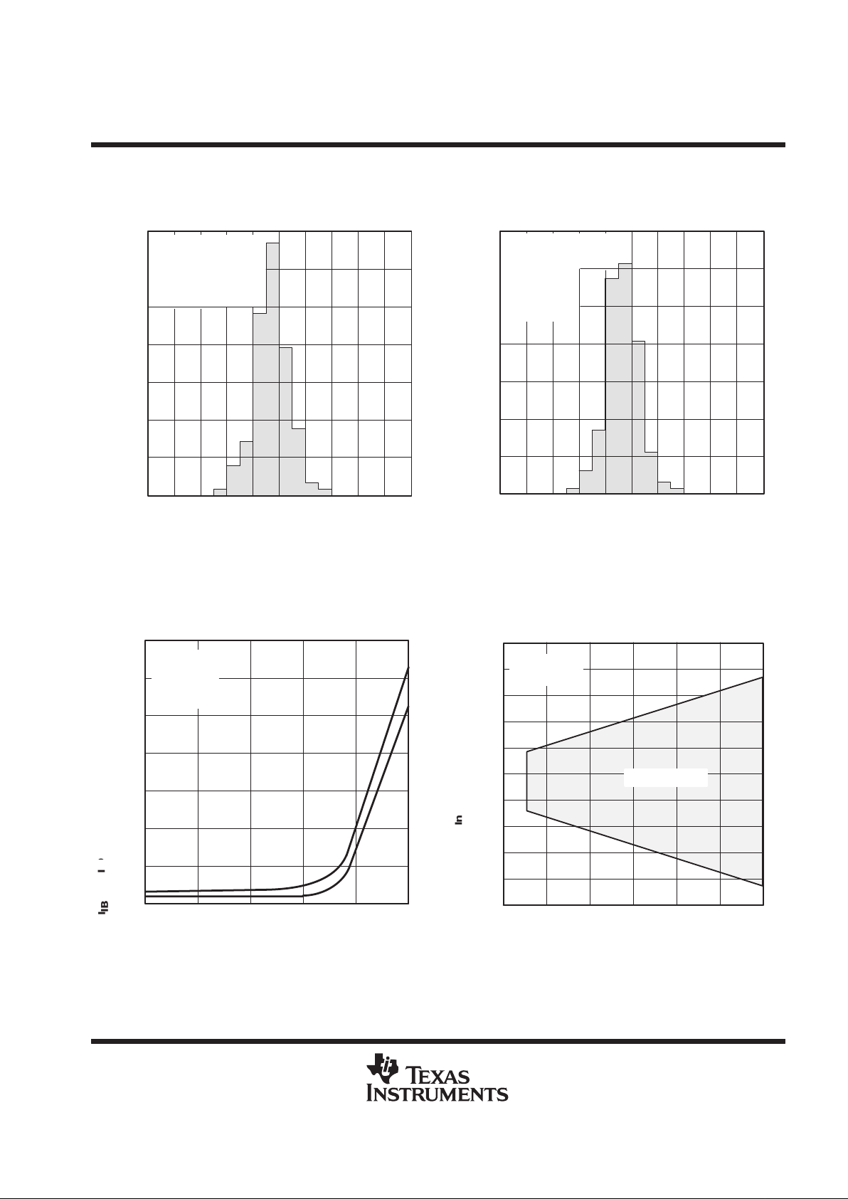
TLC226x, TLC226xA
Advanced LinCMOS RAIL-TO-RAIL
OPERATIONAL AMPLIFIERS
SLOS177A – FEBRUARY 1997 – REVISED JULY 1999
33
POST OFFICE BOX 655303 • DALLAS, TEXAS 75265
TYPICAL CHARACTERISTICS
Figure 10
Percentage of Amplifiers – %
DISTRIBUTION OF TLC2264 INPUT OFFSET
VOLTAGE TEMPERATURE COEFFICIENT
†
α
VIO
– Temperature Coefficient of
Input Offset Voltage – µV/°C
10
5
30
0
20
15
25
35
–5 –4 –3 –2 –1 0 1 2 3 4 5
128 Amplifiers From
2 Wafer Lots
V
DD±
= ± 2.5 V
N Package
TA = 25°C to 125°C
Percentage of Amplifiers – %
DISTRIBUTION OF TLC2264 INPUT OFFSET
VOLTAGE TEMPERATURE COEFFICIENT
†
α
VIO
– Temperature Coefficient of
Input Offset Voltage – µV/°C
10
5
30
0
20
15
25
35
–5 –4 –3 –2 –1 0 1 2 3 4 5
128 Amplifiers From
2 Wafer Lots
V
DD±
= ± 5 V
N Package
TA = 25°C
to 125°C
Figure 11
Figure 12
10
5
30
0
25 45 65 85
IIB and IIO – Input Bias and Input Offset Currents – pA
20
15
25
INPUT BIAS AND INPUT OFFSET CURRENTS
†
vs
FREE-AIR TEMPERATURE
35
105 125
I
IB
I
IO
V
DD±
= ±2.5 V
VIC = 0 V
VO = 0
RS = 50 Ω
TA – Free-Air Temperature – °C
I
IB
I
IO
Figure 13
0
2345
VI – Input Voltage Range – V
4
8
INPUT VOLTAGE RANGE
vs
SUPPLY VOLTAGE
10
678
6
2
–2
–4
–6
–8
–10
| VIO | ≤ 5 mV
RS = 50 Ω
TA = 25°C
V
I
| V
DD±
| – Supply Voltage – V
†
Data at high and low temperatures are applicable only within the rated operating free-air temperature ranges of the various devices.

TLC226x, TLC226xA
Advanced LinCMOS RAIL-TO-RAIL
OPERATIONAL AMPLIFIERS
SLOS177A – FEBRUARY 1997 – REVISED JULY 1999
34
POST OFFICE BOX 655303 • DALLAS, TEXAS 75265
TYPICAL CHARACTERISTICS
Figure 14
5
2
1
0
VI – Input Voltage Range – V
3
4
INPUT VOLTAGE RANGE
†‡
vs
FREE-AIR TEMPERATURE
5
–1
–75 –55 –35 –15 25 45 65 85 105 125
| VIO | ≤5 mV
VDD = 5 V
V
I
TA – Free-Air Temperature – °C
Figure 15
VOH – High-Level Output Voltage – V
HIGH-LEVEL OUTPUT VOLTAGE
†‡
vs
HIGH-LEVEL OUTPUT CURRENT
|IOH| – High-Level Output Current – µA
V
OH
3
2
1
0
0 500 1000
4
5
6
1500 2000 3000 35002500
VDD = 5 V
TA = 125°C
TA = 25°C
TA = –55°C
TA = –40°C
Figure 16
0.6
0.4
0.2
0
0123
VOL – Low-Level Output V oltage – V
0.8
1
LOW-LEVEL OUTPUT VOLTAGE
‡
vs
LOW-LEVEL OUTPUT CURRENT
1.2
45
VIC = 0
VIC = 1.25 V
VIC = 2.5 V
VDD = 5 V
TA = 25°C
V
OL
IOL – Low-Level Output Current – mA
Figure 17
0.8
0.4
0.2
0
0123
VOL – Low-Level Output V oltage – V
1
1.2
LOW-LEVEL OUTPUT VOLTAGE
†‡
vs
LOW-LEVEL OUTPUT CURRENT
1.4
456
0.6
IOL – Low-Level Output Current – mA
TA = 125°C
TA = 25°C
TA = –55°C
VDD = 5 V
VIC = 2.5 V
V
OL
TA = –40°C
†
Data at high and low temperatures are applicable only within the rated operating free-air temperature ranges of the various devices.
‡
For curves where VDD = 5 V, all loads are referenced to 2.5 V.

TLC226x, TLC226xA
Advanced LinCMOS RAIL-TO-RAIL
OPERATIONAL AMPLIFIERS
SLOS177A – FEBRUARY 1997 – REVISED JULY 1999
35
POST OFFICE BOX 655303 • DALLAS, TEXAS 75265
TYPICAL CHARACTERISTICS
Figure 18
VOM + – Maximum Positive Output Voltage – V
MAXIMUM POSITIVE OUTPUT VOLTAGE
†
vs
OUTPUT CURRENT
V
OM +
| IO | – Output Current – µA
3
2
1
0
0 500 1000
4
5
6
1500 2000 3000
35002500
V
DD±
= ±5 V
TA = 125°C
TA = 25°C
TA = –55°C
TA = –40°C
Figure 19
01 2
VOM – – Maximum Negative Output Voltage – V
MAXIMUM NEGATIVE OUTPUT VOLTAGE
†
vs
OUTPUT CURRENT
3456
–3.8
–4
–4.2
–4.4
–4.6
–4.8
–5
V
DD±
= ±5 V
VIC = 0
TA = 125°C
TA = 25°C
TA = –55°C
IO – Output Current – mA
V
OM –
TA = –40°C
6
5
3
1
0
10
4
VO(PP) – Maximum Peak-to-Peak Output Voltage – V
8
7
9
f – Frequency – Hz
MAXIMUM PEAK-TO-PEAK OUTPUT VOLTAGE
†‡
vs
FREQUENCY
2
V
O(PP)
10
3
10
4
10
5
10
6
VDD = 5 V
V
DD±
= ±5 V
RL = 10 kΩ
TA = 25°C
‡
For curves where VDD = 5 V , all loads are referenced to 2.5 V .
Figure 20 Figure 21
IOS – Short-Circuit Output Current – mA
SHORT-CIRCUIT OUTPUT CURRENT
vs
SUPPLY VOLTAGE
I
OS
| V
DD±
| – Supply Voltage – V
2345678
12
10
8
6
4
2
0
–2
–4
VID = –100 mV
VO = 0
TA = 25°C
VID = 100 mV
†
Data at high and low temperatures are applicable only within the rated operating free-air temperature ranges of the various devices.

TLC226x, TLC226xA
Advanced LinCMOS RAIL-TO-RAIL
OPERATIONAL AMPLIFIERS
SLOS177A – FEBRUARY 1997 – REVISED JULY 1999
36
POST OFFICE BOX 655303 • DALLAS, TEXAS 75265
TYPICAL CHARACTERISTICS
Figure 22
IOS – Short-Circuit Output Current – mA
SHORT-CIRCUIT OUTPUT CURRENT
†
vs
FREE-AIR TEMPERATURE
TA – Free-Air Temperature – °C
I
OS
–75
13
12
11
10
9
8
7
1
0
–1
–2
–3
–4
–50
–25
0 25 50 75 100 125
VO = 0
V
DD±
= ±5 V
VID = –100 mV
VID = 100 mV
Figure 23
3
2
1
0
0 250
4
5
OUTPUT VOLTAGE
‡
vs
DIFFERENTIAL INPUT VOLTAGE
500 750 1000
VID – Differential Input Voltage – µV
– Output Voltage – V
V
O
–1000 –750 –250–500
VDD = 5 V
RL = 50 kΩ
VIC = 2.5 V
TA = 25°C
Figure 24
1
–1
–3
–5
0 250
3
5
OUTPUT VOLTAGE
vs
DIFFERENTIAL INPUT VOLTAGE
500 750 1000
VID – Differential Input Voltage – µV
V
DD±
= ±5 V
VIC = 0 V
RL = 50 kΩ
TA = 25°C
– Output Voltage – V
V
O
–1000 –750 –250–500
1
10
Differential Gain – V/ mV
DIFFERENTIAL GAIN
‡
vs
LOAD RESISTANCE
RL – Load Resistance – kΩ
10
2
10
3
10
4
V
O(PP)
= 2 V
TA = 25°C
VDD = 5 V
10
3
10
4
10
5
10
6
V
DD±
= ±5 V
Figure 25
†
Data at high and low temperatures are applicable only within the rated operating free-air temperature ranges of the various devices.
‡
For curves where VDD = 5 V, all loads are referenced to 2.5 V.
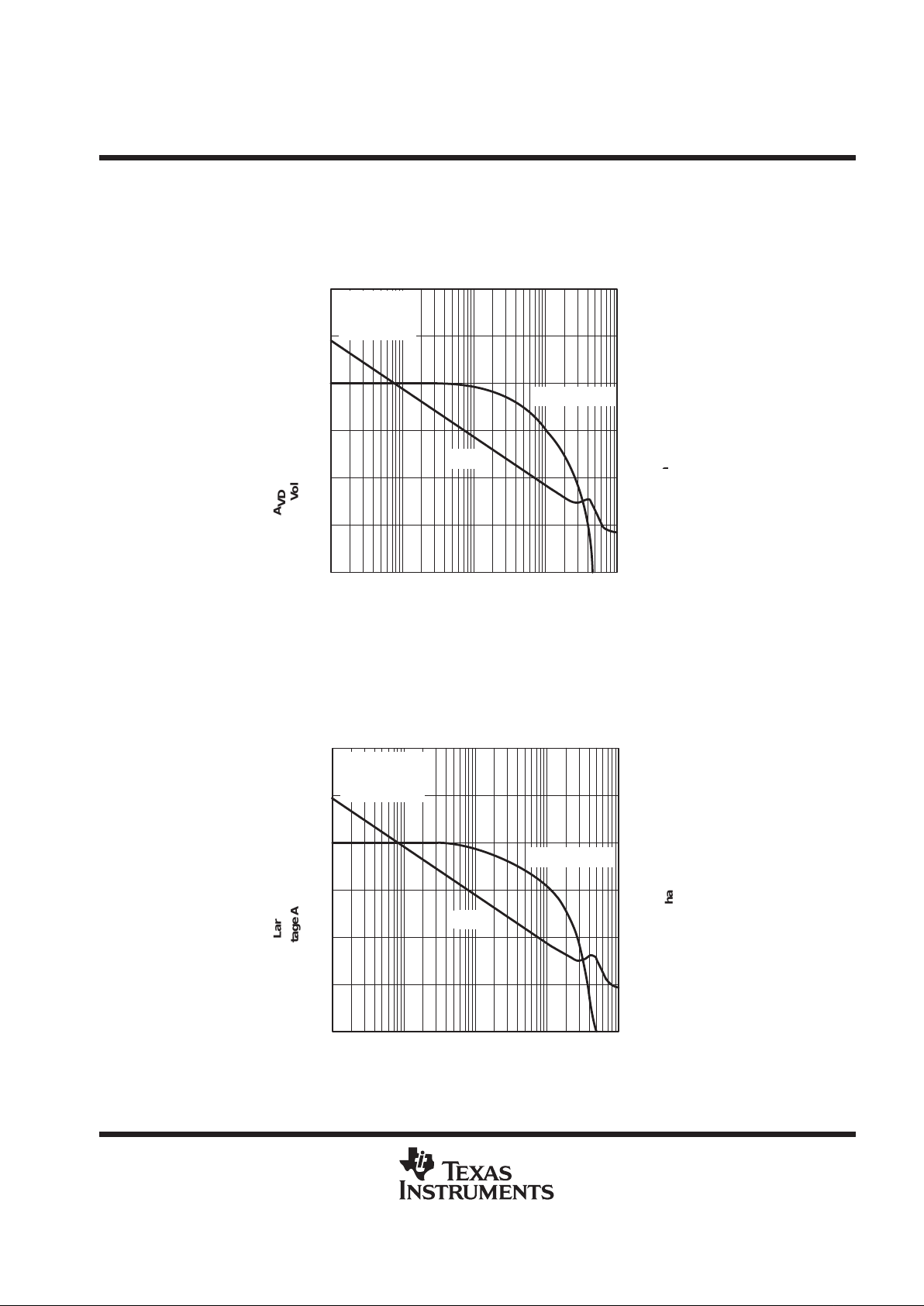
TLC226x, TLC226xA
Advanced LinCMOS RAIL-TO-RAIL
OPERATIONAL AMPLIFIERS
SLOS177A – FEBRUARY 1997 – REVISED JULY 1999
37
POST OFFICE BOX 655303 • DALLAS, TEXAS 75265
TYPICAL CHARACTERISTICS
om – Phase Margin
φ
m
20
f – Frequency – Hz
80
60
40
0
–20
–40
10
3
10
4
10
5
10
6
10
7
180°
135°
90°
45°
0°
–45°
–90°
LARGE-SIGNAL DIFFERENTIAL VOLTAGE
†
AMPLIFICATION AND PHASE MARGIN
vs
FREQUENCY
AVD – Large-Signal Differential
A
VD
Voltage Amplification – dB
†
For curves where VDD = 5 V, all loads are referenced to 2.5 V.
Gain
Phase Margin
VDD = 5 V
CL= 100 pF
TA = 25°C
Figure 26
om – Phase Margin
φ
m
20
f – Frequency – Hz
LARGE-SIGNAL DIFFERENTIAL VOLTAGE
AMPLIFICATION AND PHASE MARGIN
vs
FREQUENCY
80
60
40
0
–20
–40
10
3
10
4
10
5
10
6
10
7
180°
135°
90°
45°
0°
–45°
–90°
AVD – Large-Signal Differential
A
VD
Voltage Amplification – dB
Gain
Phase Margin
V
DD±
= ±5 V
CL = 100 pF
TA = 25°C
Figure 27

TLC226x, TLC226xA
Advanced LinCMOS RAIL-TO-RAIL
OPERATIONAL AMPLIFIERS
SLOS177A – FEBRUARY 1997 – REVISED JULY 1999
38
POST OFFICE BOX 655303 • DALLAS, TEXAS 75265
TYPICAL CHARACTERISTICS
LARGE-SIGNAL DIFFERENTIAL
VOLTAGE AMPLIFICATION
†‡
vs
FREE-AIR TEMPERATURE
–75 – 50 –25 0 25 50 75 100 125
TA – Free-Air Temperature – °C
AVD – Large-Signal Differential
A
VD
Voltage Amplification – V/mV
VDD = 5 V
VIC = 2.5 V
VO = 1 V to 4 V
RL = 50 kΩ
RL = 1 MΩ
RL = 10 kΩ
10
4
10
3
10
2
10
1
Figure 28
Figure 29
–75 –50 –25 0 25 50 75 100 125
TA – Free-Air Temperature – °C
LARGE-SIGNAL DIFFERENTIAL
VOLTAGE AMPLIFICATION
†
vs
FREE-AIR TEMPERATURE
AVD – Large-Signal Differential
A
VD
Voltage Amplification – V/mV
V
DD±
= ±5 V
VIC = 0 V
VO = ±4 V
RL = 1 MΩ
RL = 50 kΩ
RL = 10 kΩ
10
4
10
3
10
2
10
1
10
1
0.1
1000
100
zo – Output Impedance – 0
OUTPUT IMPEDANCE
‡
vs
FREQUENCY
f – Frequency – Hz
10
2
10
3
10
4
10
5
10
6
Ω
z
o
VDD = 5 V
TA = 25°C
AV = 100
AV = 10
AV = 1
Figure 30
10
1
0.1
1000
100
OUTPUT IMPEDANCE
vs
FREQUENCY
f – Frequency – Hz
10
2
10
3
10
4
10
5
10
6
V
DD±
= ±5 V
TA = 25°C
AV = 100
AV = 10
AV = 1
zo – Output Impedance – 0
Ω
z
o
Figure 31
†
Data at high and low temperatures are applicable only within the rated operating free-air temperature ranges of the various devices.
‡
For curves where VDD = 5 V, all loads are referenced to 2.5 V.

TLC226x, TLC226xA
Advanced LinCMOS RAIL-TO-RAIL
OPERATIONAL AMPLIFIERS
SLOS177A – FEBRUARY 1997 – REVISED JULY 1999
39
POST OFFICE BOX 655303 • DALLAS, TEXAS 75265
TYPICAL CHARACTERISTICS
Figure 32
60
40
20
0
80
f – Frequency – Hz
COMMON-MODE REJECTION RATIO
†
vs
FREQUENCY
100
10
1
10
2
10
3
10
4
10
5
10
6
V
DD±
= ±5 V
VDD = 5 V
CMRR – Common-Mode Rejection Ratio – dB
Figure 33
86
84
82
80
88
COMMON-MODE REJECTION RATIO
†‡
vs
FREE-AIR TEMPERATURE
90
–75 – 50 –25 0 25 50 75 100
V
DD±
= ±5 V
VDD = 5 V
TA – Free-Air Temperature – °C
CMRR – Common-Mode Rejection Ratio – dB
125
f – Frequency – Hz
SUPPLY-VOLTAGE REJECTION RATIO
†
vs
FREQUENCY
100
80
60
40
20
0
–20
10
1
10
2
10
3
10
4
10
5
10
6
k
SVR+
k
SVR–
VDD = 5 V
TA = 25°C
KSVR – Supply-Voltage Rejection Ratio – dB
k
SVR
Figure 34
KSVR – Supply-Voltage Rejection Ratio – dB
f – Frequency – Hz
SUPPLY-VOLTAGE REJECTION RATIO
vs
FREQUENCY
100
80
60
40
20
0
–20
10
1
10
2
10
3
10
4
10
5
10
6
k
SVR
k
SVR+
k
SVR–
V
DD±
= ±5 V
TA = 25°C
Figure 35
‡
Data at high and low temperatures are applicable only within the rated operating free-air temperature ranges of the various devices.
†
For curves where VDD = 5 V, all loads are referenced to 2.5 V.

TLC226x, TLC226xA
Advanced LinCMOS RAIL-TO-RAIL
OPERATIONAL AMPLIFIERS
SLOS177A – FEBRUARY 1997 – REVISED JULY 1999
40
POST OFFICE BOX 655303 • DALLAS, TEXAS 75265
TYPICAL CHARACTERISTICS
Figure 36
100
95
90
KSVR – Supply-Voltage Rejection Ratio – dB
105
SUPPLY-VOLTAGE REJECTION RATIO
†
vs
FREE-AIR TEMPERATURE
110
–50 –25 0 25 50 75 100 125
k
SVR
TA – Free-Air Temperature – °C
VO = 0
V
DD±
= ±2.2 V to ±8 V
–75
Figure 37
300
200
100
0
012345
IDD – Supply Current – uA
400
500
600
678
| V
DD±
| – Supply Voltage – V
TA = 25°C
TA = 125°C
TA = –55°C
VO = 0
No Load
I
DD
Aµ
TA = 40°C
TLC2262
SUPPLY CURRENT
†
vs
SUPPLY VOLTAGE
Figure 38
600
400
200
0
012345
IDD – Supply Current – uA
800
1000
1200
678
| V
DD±
| – Supply Voltage – V
TA = 25°C
TA = 125°C
TA = –55°C
VO = 0
No Load
I
DD
Aµ
TA = 40°C
TLC2264
SUPPLY CURRENT
†
vs
SUPPLY VOLTAGE
Figure 39
300
200
100
0
400
500
600
–75 –50 – 25 0 25 50 75 100
IDD – Supply Current – uA
I
DD
Aµ
TA – Free-Air Temperature – °C
V
DD±
= ±5 V
VO = 0
VDD = 5 V
VO = 2.5 V
125
TLC2262
SUPPLY CURRENT
†‡
vs
FREE-AIR TEMPERATURE
†
Data at high and low temperatures are applicable only within the rated operating free-air temperature ranges of the various devices.
‡
For curves where VDD = 5 V, all loads are referenced to 2.5 V.
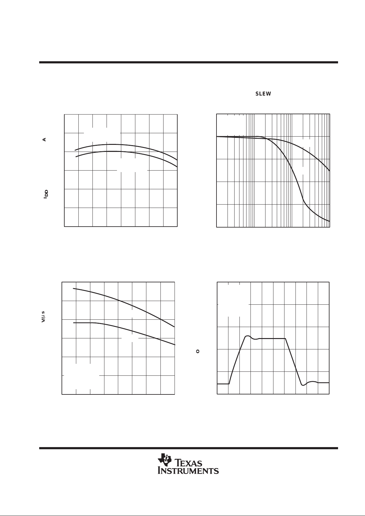
TLC226x, TLC226xA
Advanced LinCMOS RAIL-TO-RAIL
OPERATIONAL AMPLIFIERS
SLOS177A – FEBRUARY 1997 – REVISED JULY 1999
41
POST OFFICE BOX 655303 • DALLAS, TEXAS 75265
TYPICAL CHARACTERISTICS
Figure 40
600
400
200
0
800
1000
1200
–50 –25 0 25 50 75 100 125
IDD – Supply Current – uA
I
DD
Aµ
TA – Free-Air Temperature – °C
V
DD±
= ±5 V
VO = 0
VDD = 5 V
VO = 2.5 V
–75
TLC2264
SUPPLY CURRENT
†‡
vs
FREE-AIR TEMPERATURE
0.8
0.4
0.2
0
1
0.6
SR – Slew Rate – v/us
SLEW RATE
‡
vs
LOAD CAPACITANCE
sµ
V/
CL – Load Capacitance – pF
10
1
10
2
10
3
10
4
SR+
VDD = 5 V
AV = –1
TA = 25°C
SR–
Figure 41
Figure 42
0.6
0.4
0.2
0
0.8
1
SLEW RATE
†‡
vs
FREE-AIR TEMPERATURE
1.2
–75 –50 – 25 0 25 50 75 100
TA – Free-Air Temperature – °C
VDD = 5 V
RL = 50 kΩ
CL = 100 pF
AV = 1
SR – Slew Rate – v/ussµ
V/
125
SR+
SR–
Figure 43
2
1
0
0 2 4 6 8 10 12
VO – Output Voltage – V
3
4
INVERTING LARGE-SIGNAL PULSE
RESPONSE
‡
5
14 16 18 20
V
O
VDD = 5 V
RL = 50 kΩ
CL = 100 pF
AV = –1
TA = 25°C
t – Time – µs
†
Data at high and low temperatures are applicable only within the rated operating free-air temperature ranges of the various devices.
‡
For curves where VDD = 5 V, all loads are referenced to 2.5 V.

TLC226x, TLC226xA
Advanced LinCMOS RAIL-TO-RAIL
OPERATIONAL AMPLIFIERS
SLOS177A – FEBRUARY 1997 – REVISED JULY 1999
42
POST OFFICE BOX 655303 • DALLAS, TEXAS 75265
TYPICAL CHARACTERISTICS
Figure 44
0
4
024681012
2
1
3
5
14 16 18 20
V
DD±
= ±5 V
RL = 50 kΩ
CL = 100 pF
AV = –1
TA = 25°C
t – Time – µs
VO – Output Voltage – V
V
O
–1
–2
–3
–4
–5
INVERTING LARGE-SIGNAL PULSE
RESPONSE
Figure 45
2
1
0
0 2 4 6 8 10 12
3
4
VOLTAGE-FOLLOWER LARGE-SIGNAL
PULSE RESPONSE
†
5
14 16 18 20
VDD = 5 V
RL = 50 kΩ
CL = 100 pF
AV = 1
TA = 25°C
t – Time – µs
VO – Output Voltage – V
V
O
0
4
024681012
2
1
3
5
14 16 18 20
V
DD±
= ±5 V
RL = 50 kΩ
CL = 100 pF
AV = 1
TA = 25°C
t – Time – µs
VO – Output Voltage – V
V
O
–1
–2
–3
–4
–5
VOLTAGE-FOLLOWER LARGE-SIGNAL
PULSE RESPONSE
Figure 46 Figure 47
2.5
2.45
2.4
0 2 4 6 8 10 12
2.55
2.6
INVERTING SMALL-SIGNAL
PULSE RESPONSE
†
2.65
14 16 18 20
VDD = 5 V
RL = 50 kΩ
CL = 100 pF
AV = –1
TA = 25°C
VO – Output Voltage – V
V
O
t – Time – µs
†
For curves where VDD = 5 V, all loads are referenced to 2.5 V.
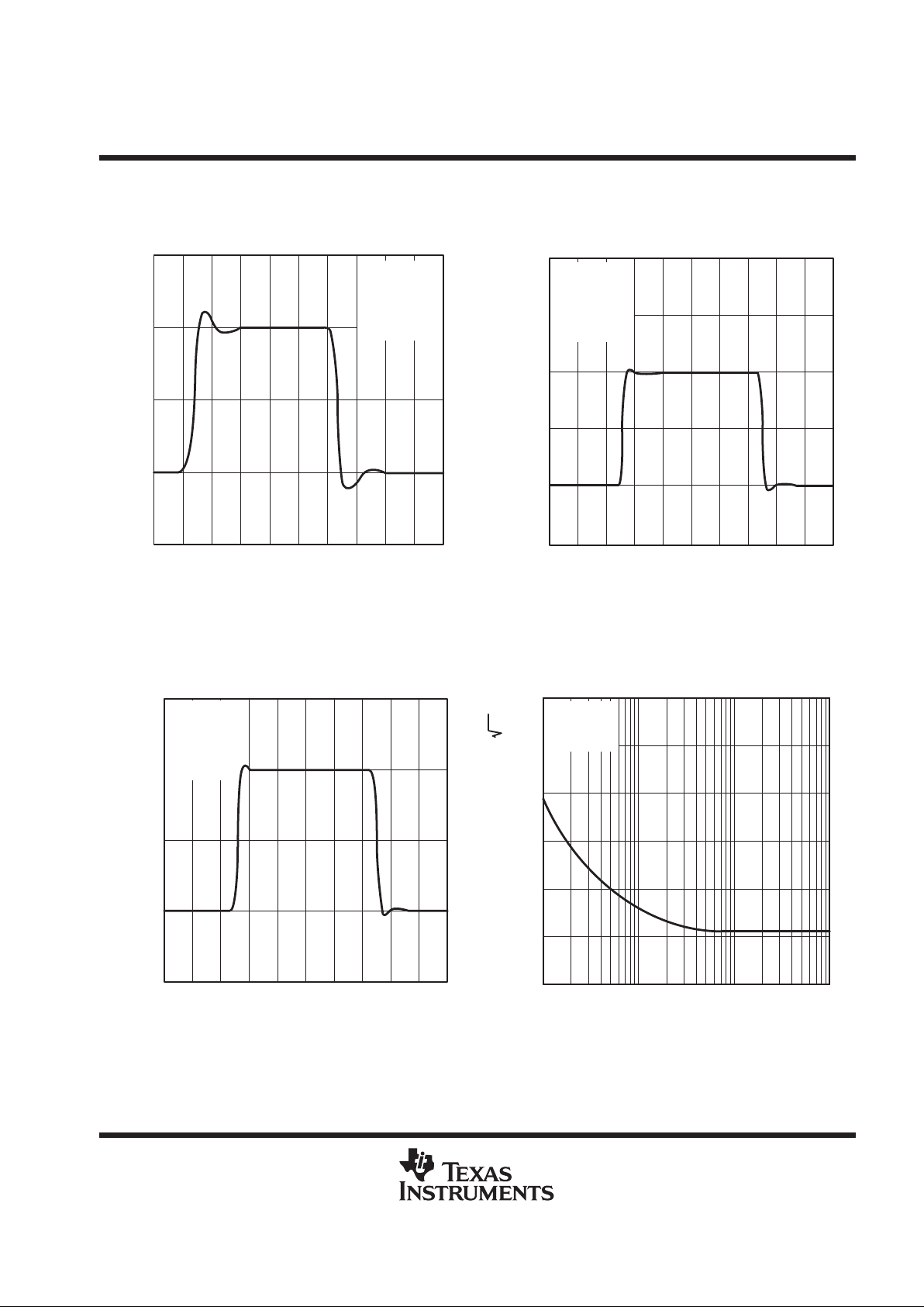
TLC226x, TLC226xA
Advanced LinCMOS RAIL-TO-RAIL
OPERATIONAL AMPLIFIERS
SLOS177A – FEBRUARY 1997 – REVISED JULY 1999
43
POST OFFICE BOX 655303 • DALLAS, TEXAS 75265
TYPICAL CHARACTERISTICS
Figure 48
0
024681012
INVERTING SMALL-SIGNAL
PULSE RESPONSE
100
14 16 18 20
50
–50
–100
V
DD±
= ±5 V
RL = 50 kΩ
CL = 100 pF
AV = –1
TA = 25°C
t – Time – µs
VO – Output Voltage – mV
V
O
Figure 49
2.5
2.45
2.4
0 2 4 6 8 10 12
2.55
2.6
VOLTAGE-FOLLOWER SMALL-SIGNAL
PULSE RESPONSE
†
2.65
14 16 18 20
VDD = 5 V
RL = 50 kΩ
CL = 100 pF
AV = 1
TA = 25°C
VO – Output Voltage – V
V
O
t – Time – µs
Figure 50
0 2 4 6 8 10 12
VOLTAGE-FOLLOWER SMALL-SIGNAL
PULSE RESPONSE
14 16 18 20
V
DD±
= ±5 V
RL = 50 kΩ
CL = 100 pF
AV = 1
TA = 25°C
VO – Output Voltage – V
V
O
t – Time – µs
–100
–50
0
50
100
40
20
10
0
60
30
VN – Equivalent Input Noise Voltage – nv//Hz
50
f – Frequency – Hz
EQUIVALENT INPUT NOISE VOLTAGE
†
vs
FREQUENCY
10
1
10
2
10
3
10
4
nV/ Hz
V
n
VDD = 5 V
RS = 20 Ω
TA = 25°C
Figure 51
†
For curves where VDD = 5 V, all loads are referenced to 2.5 V.

TLC226x, TLC226xA
Advanced LinCMOS RAIL-TO-RAIL
OPERATIONAL AMPLIFIERS
SLOS177A – FEBRUARY 1997 – REVISED JULY 1999
44
POST OFFICE BOX 655303 • DALLAS, TEXAS 75265
TYPICAL CHARACTERISTICS
40
20
10
0
60
30
50
10
1
10
2
10
3
10
4
EQUIVALENT INPUT NOISE VOLTAGE
vs
FREQUENCY
f – Frequency – Hz
VN – Equivalent Input Noise Voltage – nv//Hz
nV/ Hz
V
n
V
DD±
= ±5 V
RS = 20 Ω
TA = 25°C
Figure 52
0246
Noise Voltage – nV
0
750
t – Time – s
EQUIVALENT INPUT NOISE VOLTAGE OVER
A 10-SECOND PERIOD
†
1000
810
500
–250
–500
–750
–1000
250
VDD = 5 V
f = 0.1 Hz to 10 Hz
TA = 25°C
Figure 53
0.1
Integrated Noise Voltage –
f – Frequency – Hz
INTEGRATED NOISE VOLTAGE
vs
FREQUENCY
1
10
100
10
0
10
1
10
2
10
3
10
4
10
5
Calculated Using Ideal Pass-Band Filter
Low Frequency = 1 Hz
TA = 25°C
Vµ
Figure 54
0.01
0.1
THD + N – Total Harmonic Distortion Plus Noise – %
f – Frequency – Hz
TOTAL HARMONIC DISTORTION PLUS NOISE
†
vs
FREQUENCY
0.001
10
1
10
2
10
3
10
4
10
5
AV = 100
AV = 10
AV = 1
VDD = 5 V
RL = 50 kΩ
TA = 25°C
Figure 55
†
For curves where VDD = 5 V, all loads are referenced to 2.5 V.

TLC226x, TLC226xA
Advanced LinCMOS RAIL-TO-RAIL
OPERATIONAL AMPLIFIERS
SLOS177A – FEBRUARY 1997 – REVISED JULY 1999
45
POST OFFICE BOX 655303 • DALLAS, TEXAS 75265
TYPICAL CHARACTERISTICS
Figure 56
Gain-Bandwidth Product – kHz
GAIN-BANDWIDTH PRODUCT
vs
SUPPLY VOLTAGE
| VDD ±| – Supply Voltage – V
860
820
780
740
0235
900
940
78
146
f = 10 kHz
RL = 50 kΩ
CL = 100 pF
TA = 25°C
Figure 57
Gain-Bandwidth Product – kHz
GAIN-BANDWIDTH PRODUCT
†‡
vs
FREE-AIR TEMPERATURE
TA – Free-Air Temperature – °C
800
600
400
1000
1200
–75 –25 0 25 50 75 100 125
VDD = 5 V
f = 10 kHz
CL = 100 pF
–50
Figure 58
om – Phase Margin
PHASE MARGIN
vs
LOAD CAPACITANCE
10
1
10
2
10
3
10
4
CL – Load Capacitance – pF
m
φ
75°
60°
45°
30°
15°
0°
R
null
= 50 Ω
R
null
= 100 Ω
R
null
= 0
R
null
= 10 Ω
TA = 25°C
50 kΩ
50 kΩ
V
DD–
V
DD+
R
null
C
L
V
I
+
–
R
null
= 20 Ω
20
10
5
0
15
Gain Margin – dB
GAIN MARGIN
vs
LOAD CAPACITANCE
10
1
10
2
10
3
10
4
CL – Load Capacitance – pF
R
null
= 20 Ω
R
null
= 0
R
null
= 100 Ω
TA = 25°C
R
null
= 50 Ω
R
null
= 10 Ω
Figure 59
†
Data at high and low temperatures are applicable only within the rated operating free-air temperature ranges of the various devices.
‡
For curves where VDD = 5 V, all loads are referenced to 2.5 V.

†
See application information
TLC226x, TLC226xA
Advanced LinCMOS RAIL-TO-RAIL
OPERATIONAL AMPLIFIERS
SLOS177A – FEBRUARY 1997 – REVISED JULY 1999
46
POST OFFICE BOX 655303 • DALLAS, TEXAS 75265
TYPICAL CHARACTERISTICS
600
400
200
– Unity-Gain Bandwidth – kHz
800
UNITY-GAIN BANDWIDTH
†
vs
LOAD CAPACITANCE
1000
10
1
10
2
10
3
10
4
CL – Load Capacitance – pF
B
1
TA = 25°C
Figure 60
Overestimation of Phase Margin
OVERESTIMATION OF PHASE MARGIN
†
vs
LOAD CAPACITANCE
14°
12°
10°
6°
4°
0
2°
10
1
10
2
10
3
10
4
CL – Load Capacitance – pF
R
null
= 100 Ω
R
null
= 50 Ω
R
null
= 10 Ω
TA = 25°C
R
null
= 20 Ω
8°
Figure 61

TLC226x, TLC226xA
Advanced LinCMOS RAIL-TO-RAIL
OPERATIONAL AMPLIFIERS
SLOS177A – FEBRUARY 1997 – REVISED JULY 1999
47
POST OFFICE BOX 655303 • DALLAS, TEXAS 75265
APPLICATION INFORMATION
driving large capacitive loads
The TLC226x is designed to drive larger capacitive loads than most CMOS operational amplifiers. Figure 58
and Figure 59 illustrate its ability to drive loads greater than 400 pF while maintaining good gain and phase
margins (R
null
= 0).
A smaller series resistor (R
null
) at the output of the device (see Figure 62) improves the gain and phase margins
when driving large capacitive loads. Figure 58 and Figure 59 show the effects of adding series resistances of
10 Ω, 20 Ω, 50 Ω, and 100 Ω. The addition of this series resistor has two effects: the first is that it adds a zero
to the transfer function and the second is that it reduces the frequency of the pole associated with the output
load in the transfer function.
The zero introduced to the transfer function is equal to the series resistance times the load capacitance. To
calculate the improvement in phase margin, equation 1 can be used.
∆Θm1+
tan
–1
ǒ
2 × π × UGBW × R
null
× C
L
Ǔ
where :
(1)
∆Θm1+
improvementinphasemargin
UGBW+unity-gainbandwidthfrequency
R
null
+
outputseriesresistance
CL+
loadcapacitance
The unity-gain bandwidth (UGBW) frequency decreases as the capacitive load increases (see Figure 60). To
use equation 1, UGBW must be approximated from Figure 60.
Using equation 1 alone overestimates the improvement in phase margin, as illustrated in Figure 61. The
overestimation is caused by the decrease in the frequency of the pole associated with the load, thus providing
additional phase shift and reducing the overall improvement in phase margin. The pole associated with the load
is reduced by the factor calculated in equation 2.
F
+
1
1)g
m
×
R
null
Where :
(2)
F+factorreducingfrequencyofpole
gm+
small-signaloutputtransconductance(typically 4.83 × 10⁻³mhos)
R
null
+
output series resistance
For the TLC226x, the pole associated with the load is typically 7 MHz with 100-pF load capacitance. This value
varies inversely with CL: at CL = 10 pF, use 70 MHz, at CL = 1000 pF, use 700 kHz, and so on.
Reducing the pole associated with the load introduces phase shift, thereby reducing phase margin. This results
in an error in the increase in phase margin expected by considering the zero alone (equation 1). Equation 3
approximates the reduction in phase margin due to the movement of the pole associated with the load. The
result of this equation can be subtracted from the result of the equation in equation 1 to better approximate the
improvement in phase margin.

TLC226x, TLC226xA
Advanced LinCMOS RAIL-TO-RAIL
OPERATIONAL AMPLIFIERS
SLOS177A – FEBRUARY 1997 – REVISED JULY 1999
48
POST OFFICE BOX 655303 • DALLAS, TEXAS 75265
APPLICATION INFORMATION
driving large capacitive loads (continued)
∆Θm2+
tan
–1
ȧ
ȱ
Ȳ
UGBW
ǒ
F×P
2
Ǔ
ȧ
ȳ
ȴ
–tan
–1
ǒ
UGBW
P
2
Ǔ
Where :
(3)
∆Θm2+
reduction in phase margin
UGBW+unity-gain bandwidth frequency
F+factor from equation 2
P2+
unadjusted pole (70 MHz@10 pF, 7 MHz@100 pF, etc.)
Using these equations with Figure 60 and Figure 61 enables the designer to choose the appropriate output
series resistance to optimize the design of circuits driving large capacitive loads.
50 kΩ
50 kΩ
V
DD–/GND
V
DD+
R
null
C
L
V
I
+
–
Figure 62. Series-Resistance Circuit

TLC226x, TLC226xA
Advanced LinCMOS RAIL-TO-RAIL
OPERATIONAL AMPLIFIERS
SLOS177A – FEBRUARY 1997 – REVISED JULY 1999
49
POST OFFICE BOX 655303 • DALLAS, TEXAS 75265
APPLICATION INFORMATION
macromodel information
Macromodel information provided was derived using Microsim
Parts
, the model generation software used
with Microsim
PSpice
. The Boyle macromodel (see Note 5) and subcircuit in Figure 63 are generated using
the TLC226x typical electrical and operating characteristics at T
A
= 25°C. Using this information, output
simulations of the following key parameters can be generated to a tolerance of 20% (in most cases):
D
Maximum positive output voltage swing
D
Maximum negative output voltage swing
D
Slew rate
D
Quiescent power dissipation
D
Input bias current
D
Open-loop voltage amplification
D
Unity-gain frequency
D
Common-mode rejection ratio
D
Phase margin
D
DC output resistance
D
AC output resistance
D
Short-circuit output current limit
NOTE 5: G. R. Boyle, B. M. Cohn, D. O. Pederson, and J. E. Solomon, “Macromodeling of Intergrated Circuit Operational Amplifiers,”
IEEE
Journal of Solid-State Circuits,
SC-9, 353 (1974).
OUT
+
–
+
–
+
–
+
–
+
–
+
–
+
–
+
–
+–
.SUBCKT TLC226x 1 2 3 4 5
C1 11 12 3.560E–12
C2 6 7 15.00E–12
DC 5 53 DX
DE 54 5 DX
DLP 90 91 DX
DLN 92 90 DX
DP 43DX
EGND 99 0 POLY (2) (3,0) (4,0) 0 .5 .5
FB 7 99 POLY (5) VB VC VE VLP
+ VLN 0 21.04E6 –30E6 30E6 30E6 –30E6
GA 6 0 11 12 47.12E–6
GCM 0 6 10 99 4.9E–9
ISS 3 10 DC 8.250E–6
HLIM 90 0 VLIM 1K
J1 11 2 10 JX
J2 12 1 10 JX
R2 6 9 100.0E3
RD1 60 11 21.22E3
RD2 60 12 21.22E3
R01 8 5 120
R02 7 99 120
RP 3 4 26.04E3
RSS 10 99 24.24E6
VAD 60 4 –.6
VB 9 0 DC 0
VC 3 53 DC .65
VE 54 4 DC .65
VLIM 7 8 DC 0
VLP 91 0 DC 1.4
VLN 0 92 DC 9.4
.MODEL DX D (IS=800.0E–18)
.MODEL JX PJF (IS=500.0E–15 BETA=281E–6
+ VTO=–.065)
.ENDS
V
CC+
RP
IN –
2
IN+
1
V
CC–
VAD
RD1
11
J1 J2
10
RSS ISS
3
12
RD2
60
VE
54
DE
DP
VC
DC
4
C1
53
R2
6
9
EGND
VB
FB
C2
GCM
GA
VLIM
8
5
RO1
RO2
HLIM
90
DLP
91
DLN
92
VLNVLP
99
7
Figure 63. Boyle Macromodel and Subcircuit
PSpice
and
Parts
are trademarks of MicroSim Corporation.

TLC226x, TLC226xA
Advanced LinCMOS RAIL-TO-RAIL
OPERATIONAL AMPLIFIERS
SLOS177A – FEBRUARY 1997 – REVISED JULY 1999
50
POST OFFICE BOX 655303 • DALLAS, TEXAS 75265
MECHANICAL INFORMATION
D (R-PDSO-G**) PLASTIC SMALL-OUTLINE PACKAGE
14 PIN SHOWN
4040047/B 03/95
0.228 (5,80)
0.244 (6,20)
0.069 (1,75) MAX
0.010 (0,25)
0.004 (0,10)
1
14
0.014 (0,35)
0.020 (0,51)
A
0.157 (4,00)
0.150 (3,81)
7
8
0.044 (1,12)
0.016 (0,40)
Seating Plane
0.010 (0,25)
PINS **
0.008 (0,20) NOM
A MIN
A MAX
DIM
Gage Plane
0.189
(4,80)
(5,00)
0.197
8
(8,55)
(8,75)
0.337
14
0.344
(9,80)
16
0.394
(10,00)
0.386
0.004 (0,10)
M
0.010 (0,25)
0.050 (1,27)
0°–8°
NOTES: A. All linear dimensions are in inches (millimeters).
B. This drawing is subject to change without notice.
C. Body dimensions do not include mold flash or protrusion, not to exceed 0.006 (0,15).
D. Four center pins are connected to die mount pad.
E. Falls within JEDEC MS-012

TLC226x, TLC226xA
Advanced LinCMOS RAIL-TO-RAIL
OPERATIONAL AMPLIFIERS
SLOS177A – FEBRUARY 1997 – REVISED JULY 1999
51
POST OFFICE BOX 655303 • DALLAS, TEXAS 75265
MECHANICAL INFORMATION
FK (S-CQCC-N**) LEADLESS CERAMIC CHIP CARRIER
4040140/C 11/95
28 TERMINAL SHOWN
B
0.358
(9,09)
MAX
(11,63)
0.560
(14,22)
0.560
0.458
0.858
(21,8)
1.063
(27,0)
(14,22)
A
NO. OF
MINMAX
0.358
0.660
0.761
0.458
0.342
(8,69)
MIN
(11,23)
(16,26)
0.640
0.740
0.442
(9,09)
(11,63)
(16,76)
0.962
1.165
(23,83)
0.938
(28,99)
1.141
(24,43)
(29,59)
(19,32)(18,78)
**
20
28
52
44
68
84
0.020 (0,51)
TERMINALS
0.080 (2,03)
0.064 (1,63)
(7,80)
0.307
(10,31)
0.406
(12,58)
0.495
(12,58)
0.495
(21,6)
0.850
(26,6)
1.047
0.045 (1,14)
0.045 (1,14)
0.035 (0,89)
0.035 (0,89)
0.010 (0,25)
12
1314151618 17
11
10
8
9
7
5
432
0.020 (0,51)
0.010 (0,25)
6
12826 27
19
21
B SQ
A SQ
22
23
24
25
20
0.055 (1,40)
0.045 (1,14)
0.028 (0,71)
0.022 (0,54)
0.050 (1,27)
NOTES: A. All linear dimensions are in inches (millimeters).
B. This drawing is subject to change without notice.
C. This package can be hermetically sealed with a metal lid.
D. The terminals are gold plated.
E. Falls within JEDEC MS-004

TLC226x, TLC226xA
Advanced LinCMOS RAIL-TO-RAIL
OPERATIONAL AMPLIFIERS
SLOS177A – FEBRUARY 1997 – REVISED JULY 1999
52
POST OFFICE BOX 655303 • DALLAS, TEXAS 75265
MECHANICAL INFORMATION
J (R-GDIP-T**) CERAMIC DUAL-IN-LINE PACKAGE
4040083/B 04/95
14 PIN SHOWN
22
0.410
(10,41)
0.390
(28,00)
1.100
(9,91)
0.388
(9,65)
20181614
PINS **
0.310
(7,87)
0.290
0.755
(19,18)
(19,94)
0.785
(7,37)
0.310
(7,87)
(7,37)
0.290
(23,10)
0.910
0.300
(7,62)
(6,22)
0.245
A
0.300
(7,62)
(6,22)
0.245
0.290
(7,87)
0.310
0.785
(19,94)
(19,18)
0.755
(7,37)
A MIN
A MAX
B MAX
B MIN
0.245
(6,22)
(7,11)
0.280
C MIN
C MAX
DIM
0.245
(6,22)
(7,62)
0.300
0.975
(24,77)
(23,62)
0.930
0.290
(7,37)
(7,87)
0.310
Seating Plane
0.014 (0,36)
0.008 (0,20)
C
8
7
0.020 (0,51) MIN
B
0.070 (1,78)
0.100 (2,54)
0.065 (1,65)
0.045 (1,14)
14
1
0.015 (0,38)
0.023 (0,58)
0.200 (5,08) MAX
0.130 (3,30) MIN
0.100 (2,54)
0°–15°
NOTES: A. All linear dimensions are in inches (millimeters).
B. This drawing is subject to change without notice.
C. This package can be hermetically sealed with a ceramic lid using glass frit.
D. Index point is provided on cap for terminal identification only on press ceramic glass frit seal only.
E. Falls within MIL-STD-1835 GDIP1-T14, GDIP1-T16, GDIP1-T18, GDIP1-T20, and GDIP1-T22

TLC226x, TLC226xA
Advanced LinCMOS RAIL-TO-RAIL
OPERATIONAL AMPLIFIERS
SLOS177A – FEBRUARY 1997 – REVISED JULY 1999
53
POST OFFICE BOX 655303 • DALLAS, TEXAS 75265
MECHANICAL INFORMATION
JG (R-GDIP-T8) CERAMIC DUAL-IN-LINE PACKAGE
4040107/B 04/95
0.020 (0,51) MIN
0.200 (5,08) MAX
0.130 (3,30) MIN
14
58
0°–15°
0.008 (0,20)
0.310 (7,87)
0.290 (7,37)
0.245 (6,22)
0.280 (7,11)
Seating Plane
0.015 (0,38)
0.015 (0,38)
0.023 (0,58)
0.400 (10,20)
0.355 (9,00)
0.063 (1,60)
0.015 (0,38)
0.065 (1,65)
0.045 (1,14)
0.100 (2,54)
NOTES: A. All linear dimensions are in inches (millimeters).
B. This drawing is subject to change without notice.
C. This package can be hermetically sealed with a ceramic lid using glass frit.
D. Index point is provided on cap for terminal identification only on press ceramic glass frit seal only
E. Falls within MIL-STD-1835 GDIP1-T8

TLC226x, TLC226xA
Advanced LinCMOS RAIL-TO-RAIL
OPERATIONAL AMPLIFIERS
SLOS177A – FEBRUARY 1997 – REVISED JULY 1999
54
POST OFFICE BOX 655303 • DALLAS, TEXAS 75265
MECHANICAL INFORMATION
N (R-PDIP-T**) PLASTIC DUAL-IN-LINE PACKAGE
20
0.975
(24,77)
0.940
(23,88)
18
0.920
0.850
14
0.775
0.745
(19,69)
(18,92)
16
0.775
(19,69)
(18,92)
0.745
A MIN
DIM
A MAX
PINS **
0.310 (7,87)
0.290 (7,37)
(23.37)
(21.59)
Seating Plane
0.010 (0,25) NOM
14/18 PIN ONL Y
4040049/C 08/95
9
8
0.070 (1,78) MAX
A
0.035 (0,89) MAX
0.020 (0,51) MIN
16
1
0.015 (0,38)
0.021 (0,53)
0.200 (5,08) MAX
0.125 (3,18) MIN
0.240 (6,10)
0.260 (6,60)
M
0.010 (0,25)
0.100 (2,54)
0°–15°
16 PIN SHOWN
NOTES: A. All linear dimensions are in inches (millimeters).
B. This drawing is subject to change without notice.
C. Falls within JEDEC MS-001 (20 pin package is shorter then MS-001.)

TLC226x, TLC226xA
Advanced LinCMOS RAIL-TO-RAIL
OPERATIONAL AMPLIFIERS
SLOS177A – FEBRUARY 1997 – REVISED JULY 1999
55
POST OFFICE BOX 655303 • DALLAS, TEXAS 75265
MECHANICAL INFORMATION
P (R-PDIP-T8) PLASTIC DUAL-IN-LINE PACKAGE
4040082/B 03/95
0.310 (7,87)
0.290 (7,37)
0.010 (0,25) NOM
0.400 (10,60)
0.355 (9,02)
58
41
0.020 (0,51) MIN
0.070 (1,78) MAX
0.240 (6,10)
0.260 (6,60)
0.200 (5,08) MAX
0.125 (3,18) MIN
0.015 (0,38)
0.021 (0,53)
Seating Plane
M
0.010 (0,25)
0.100 (2,54)
0°–15°
NOTES: A. All linear dimensions are in inches (millimeters).
B. This drawing is subject to change without notice.
C. Falls within JEDEC MS-001

TLC226x, TLC226xA
Advanced LinCMOS RAIL-TO-RAIL
OPERATIONAL AMPLIFIERS
SLOS177A – FEBRUARY 1997 – REVISED JULY 1999
56
POST OFFICE BOX 655303 • DALLAS, TEXAS 75265
MECHANICAL INFORMATION
PW (R-PDSO-G**) PLASTIC SMALL-OUTLINE PACKAGE
4040064/D 10/95
14 PIN SHOWN
Seating Plane
0,10 MIN
1,20 MAX
1
A
7
14
0,19
4,50
4,30
8
6,10
6,70
0,32
0,75
0,50
0,25
Gage Plane
0,15 NOM
0,65
M
0,13
0°–8°
0,10
PINS **
A MIN
A MAX
DIM
2,90
3,10
8
4,90
5,10
14
6,60
6,404,90
5,10
16
7,70
20
7,90
24
9,60
9,80
28
NOTES: A. All linear dimensions are in millimeters.
B. This drawing is subject to change without notice.
C. Body dimensions do not include mold flash or protrusion not to exceed 0,15.
D. Falls within JEDEC MO-153

TLC226x, TLC226xA
Advanced LinCMOS RAIL-TO-RAIL
OPERATIONAL AMPLIFIERS
SLOS177A – FEBRUARY 1997 – REVISED JULY 1999
57
POST OFFICE BOX 655303 • DALLAS, TEXAS 75265
MECHANICAL INFORMATION
U (S-GDFP-F10) CERAMIC DUAL FLATPACK
4040179/B 03/95
1.000 (25,40)
0.080 (2,03)
0.250 (6,35)
0.250 (6,35)
0.019 (0,48)
0.025 (0,64)
0.300 (7,62)
0.045 (1,14)
0.006 (0,15)
0.050 (1,27)
0.015 (0,38)
0.005 (0,13)
0.026 (0,66)
0.004 (0,10)
0.246 (6,10)
0.750 (19,05)
1
10
5
6
0.250 (6,35)
0.350 (8,89)0.350 (8,89)
0.250 (6,35)
0.050 (1,27)
NOTES: A. All linear dimensions are in inches (millimeters).
B. This drawing is subject to change without notice.
C. This package can be hermetically sealed with a ceramic lid using glass frit.
D. Index point is provided on cap for terminal identification only.
E. Falls within MIL STD 1835 GDFP1-F10 and JEDEC MO-092AA

TLC226x, TLC226xA
Advanced LinCMOS RAIL-TO-RAIL
OPERATIONAL AMPLIFIERS
SLOS177A – FEBRUARY 1997 – REVISED JULY 1999
58
POST OFFICE BOX 655303 • DALLAS, TEXAS 75265
MECHANICAL INFORMATION
W (R-GDFP-F16) CERAMIC DUAL FLATPACK
0.235 (5,97)
0.355 (9,02) 0.355 (9,02)
0.235 (5,97)
98
161
0.745 (18,92)
0.245 (6,22)
0.004 (0,10)
0.026 (0,66)
0.015 (0,38)
0.015 (0,38)
0.045 (1,14)
0.371 (9,42)
0.006 (0,15)
0.045 (1,14)
Base and Seating Plane
0.025 (0,64)
0.019 (0,48)
0.440 (11,18)
0.285 (7,24)
0.085 (2,16)
1.025 (26,04)
4040180-3/B 03/95
0.275 (6,99)
0.305 (7,75)
0.050 (1,27)
NOTES: A. All linear dimensions are in inches (millimeters).
B. This drawing is subject to change without notice.
C. This package can be hermetically sealed with a ceramic lid using glass frit.
D. Index point is provided on cap for terminal identification only.
E. Falls within MIL-STD-1835 GDFP1-F16 and JEDEC MO-092AC

IMPORTANT NOTICE
T exas Instruments and its subsidiaries (TI) reserve the right to make changes to their products or to discontinue
any product or service without notice, and advise customers to obtain the latest version of relevant information
to verify, before placing orders, that information being relied on is current and complete. All products are sold
subject to the terms and conditions of sale supplied at the time of order acknowledgement, including those
pertaining to warranty, patent infringement, and limitation of liability.
TI warrants performance of its semiconductor products to the specifications applicable at the time of sale in
accordance with TI’s standard warranty. Testing and other quality control techniques are utilized to the extent
TI deems necessary to support this warranty. Specific testing of all parameters of each device is not necessarily
performed, except those mandated by government requirements.
CERT AIN APPLICATIONS USING SEMICONDUCTOR PRODUCTS MAY INVOLVE POTENTIAL RISKS OF
DEATH, PERSONAL INJURY, OR SEVERE PROPERTY OR ENVIRONMENTAL DAMAGE (“CRITICAL
APPLICATIONS”). TI SEMICONDUCTOR PRODUCTS ARE NOT DESIGNED, AUTHORIZED, OR
WARRANTED TO BE SUITABLE FOR USE IN LIFE-SUPPORT DEVICES OR SYSTEMS OR OTHER
CRITICAL APPLICATIONS. INCLUSION OF TI PRODUCTS IN SUCH APPLICA TIONS IS UNDERSTOOD T O
BE FULLY AT THE CUSTOMER’S RISK.
In order to minimize risks associated with the customer’s applications, adequate design and operating
safeguards must be provided by the customer to minimize inherent or procedural hazards.
TI assumes no liability for applications assistance or customer product design. TI does not warrant or represent
that any license, either express or implied, is granted under any patent right, copyright, mask work right, or other
intellectual property right of TI covering or relating to any combination, machine, or process in which such
semiconductor products or services might be or are used. TI’s publication of information regarding any third
party’s products or services does not constitute TI’s approval, warranty or endorsement thereof.
Copyright 1999, Texas Instruments Incorporated
 Loading...