

TL461
PRECISION SERIES REFERENCE
SLVS263 – NOVEMBER 1999
1
POST OFFICE BOX 655303 • DALLAS, TEXAS 75265
D
Low Drift . . . 30 ppm/°C (max)
D
"
0.5% Output-Voltage Tolerance
D
Low Quiescent Current . . . 180 µA (max)
D
Shutdown Feature
D
Standby Current . . . –50 µA (max)
D
Packaged In Plastic SOT-23 Package
description
The TL461 is a precision series voltage reference with a very low temperature drift of 30 ppm/°C, and
an output voltage tolerance of 0.5%. The TL461 offers a power-saving advantage over three-terminal precision
shunt regulators and voltage references that must conduct the full-load current when operated in the
reverse-breakdown region. In addition, the shutdown feature of the device provides low standby current. This
device is ideal for use with handheld and battery-operated equipment, switching power supplies, dc-dc
converters, A/D and D/A converters, and in low-power precision regulator applications.
The TL461 device is characterized for operation from –40°C to 85°C.
Please be aware that an important notice concerning availability, standard warranty, and use in critical applications of
Texas Instruments semiconductor products and disclaimers thereto appears at the end of this data sheet.
PRODUCT PREVIEW
PRODUCT PREVIEW information concerns products in the formative or
design phase of development. Characteristic data and other
specifications are design goals. Texas Instruments reserves the right to
change or discontinue these products without notice.
Copyright 1999, Texas Instruments Incorporated
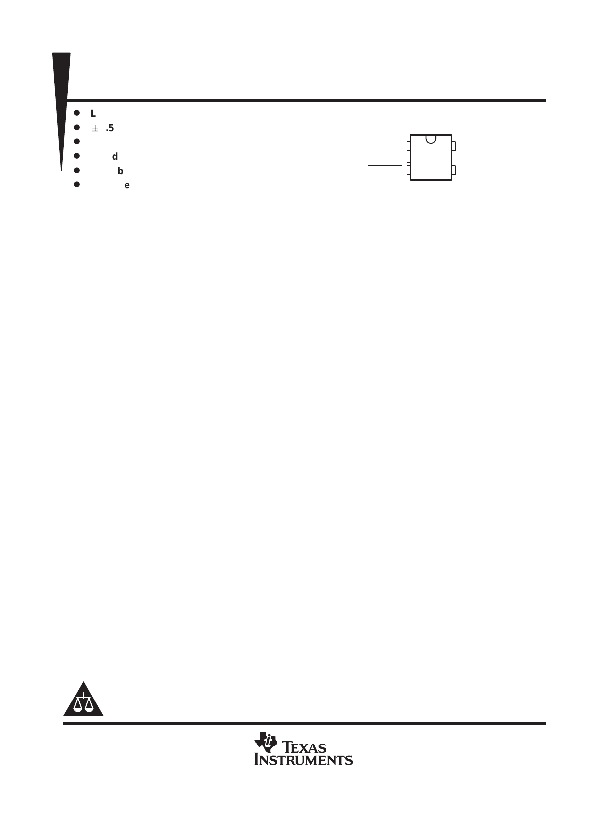
DBV PACKAGE
(TOP VIEW)
1
2
3
5
4
NC
GND
ENABLE
OUTPUT
INPUT
TL461
PRECISION SERIES REFERENCE
SLVS263 – NOVEMBER 1999
2
POST OFFICE BOX 655303 • DALLAS, TEXAS 75265
absolute maximum ratings over operating free-air temperature range (unless otherwise noted)
†
Input voltage 30 V. . . . . . . . . . . . . . . . . . . . . . . . . . . . . . . . . . . . . . . . . . . . . . . . . . . . . . . . . . . . . . . . . . . . . . . . . . . . . .
Package thermal impedance, θJA (see Note 1) 347°C/W. . . . . . . . . . . . . . . . . . . . . . . . . . . . . . . . . . . . . . . . . . . .
Operating virtual junction temperature range, TJ 0°C to 150°C. . . . . . . . . . . . . . . . . . . . . . . . . . . . . . . . . . . . . . .
Lead temperature 1,6 mm (1/16 inch) from case for 10 seconds 260°C. . . . . . . . . . . . . . . . . . . . . . . . . . . . . . .
Storage temperature range, T
stg
–65°C to 150°C. . . . . . . . . . . . . . . . . . . . . . . . . . . . . . . . . . . . . . . . . . . . . . . . . . .
†
Stresses beyond those listed under “absolute maximum ratings” may cause permanent damage to the device. These are stress ratings only, and
functional operation of the device at these or any other conditions beyond those indicated under “recommended operating conditions” is not
implied. Exposure to absolute-maximum-rated conditions for extended periods may affect device reliability.
NOTE 1: Package thermal impedance is calculated in accordance with JESD 51.
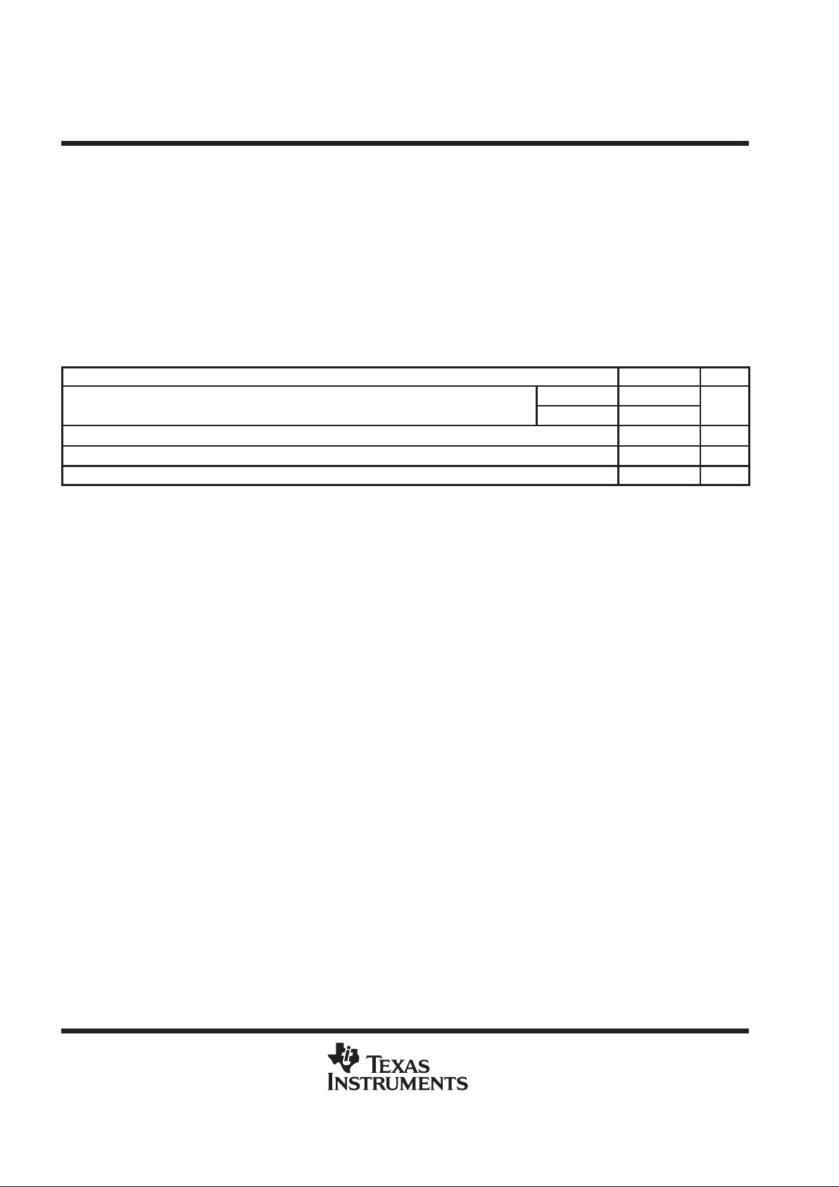
recommended operating conditions
MIN MAX UNIT
p
TL461-33 4.7
In ut voltage, V
I
TL461-05 6.4
V
Output current, I
O
20 mA
Operating free-air temperature range, T
A
–40 85 °C
Operating virtual-junction temperature range, T
J
0 125 °C
PRODUCT PREVIEW

TL461
PRECISION SERIES REFERENCE
SLVS263 – NOVEMBER 1999
3
POST OFFICE BOX 655303 • DALLAS, TEXAS 75265
electrical characteristics at 25°C free-air temperature, Vin = V
out
+ 2.5 V, I
out
= 0
(unless otherwise noted)
PARAMETER TEST CONDITIONS T
A
MIN TYP MAX UNIT
p
TL461-33 25°C 3.284 3.3 3.317
VOOutput voltage
TL461-05 25°C 4.975 5 5.025
V
α
V
out
Output voltage temperature
coefficient (see Note 2)
T
min
< Tj < T
max
–40°C to 85°C 10 30 ppm/°C
25°C 3.1 6.3
n
V
O
Line regulation
7.5 V
<
V
in
< 20
V
–40°C to 85°C 8.1
m
V
25°C 2.2 3
I
out
=
100 µA
–40°C to 85°C 4
25°C 14 27
n
VOLoad regulation sourcing
I
out
= 10
mA
–40°C to 85°C 35
mV
25°C 22 40
I
out
= 20
mA
–40°C to 85°C 50
Dropout voltage I
out
= 10 mA –40°C to 85°C 1.4 V
I
O
Output current V
out
= GND 25°C 40 mA
Reverse leakage Vin = –15 V –40°C to 85°C 0.5 10 µA
25°C 125 180
Quiescent current
–40°C to 85°C 225
µ
A
Standby current –40°C to 85°C 50 µA
ENABLE = 0.8 V
°
°
7
ENABLE bi
as current
ENABLE = 2 V
–
40°C to 85°C
0.05
µ
A
p
0.1 Hz < f < 10 Hz
°
20 µV
pp
Output noise voltage (see Note 3)
10 Hz < f < 1 kHz
25°C
20 µV
rms
Long-term stability of output voltage (see Note 4) 25°C 70
ppm/√k
Hz
NOTES: 2. Temperature coefficient is measured by dividing the change in output voltage by the specified temperature range.
Maximum V
out
Minimum V
out
∆T
A
∆V
out
Ť
a
V
out
Ť
ǒ
ppm
°C
Ǔ
+
ǒ
D
V
out
V
out
at 25°C
Ǔ
10
6
D
T
A
Where:
∆TA is the recommended operating free-air temperature range of the device.
can be positive or negative, depending on whether minimum V
out
or maximum V
out
, respectively,
occurs at the lower temperature.
a
V
out
3. Peak-to-peak noise is measured with a single high-pass filter at 0.1 Hz and two-pole low-pass filter at 10 Hz. The unit is enclosed
in a still-air environment to eliminate thermocouple effects on the leads. The test time is 10 seconds. RMS noise is measured with
a single high-pass filter at 10 Hz and a two-pole low-pass filter at 1 kHz. The resulting output is full-wave rectified, then integrated
for a fixed period, making the final reading an average rather than RMS. A correction factor of 1.1 converts from average to RMS.
A second correction of 0.88 corrects for the nonideal bandpass of the filters.
4. Long-term stability typically has a logarithmic characteristic. Therefore, stability changes after 1000 hours tend to be much smaller
than before that time. T otal drift in the second thousand hours is normally less than one third of that of the first thousand hours, with
a continuing trend toward reduced drift with time. Significant improvement in long-term drift can be realized by preconditioning the
device with a 100-hour to 200-hour, 125°C burn-in. Long-term stability also is affected by dif ferential stresses between the device
and the board material that are created during board assembly.
PRODUCT PREVIEW

IMPORTANT NOTICE
T exas Instruments and its subsidiaries (TI) reserve the right to make changes to their products or to discontinue
any product or service without notice, and advise customers to obtain the latest version of relevant information
to verify, before placing orders, that information being relied on is current and complete. All products are sold
subject to the terms and conditions of sale supplied at the time of order acknowledgement, including those
pertaining to warranty, patent infringement, and limitation of liability.
TI warrants performance of its semiconductor products to the specifications applicable at the time of sale in
accordance with TI’s standard warranty. Testing and other quality control techniques are utilized to the extent
TI deems necessary to support this warranty. Specific testing of all parameters of each device is not necessarily
performed, except those mandated by government requirements.
CERT AIN APPLICATIONS USING SEMICONDUCT OR PRODUCTS MAY INVOLVE POTENTIAL RISKS OF
DEATH, PERSONAL INJURY, OR SEVERE PROPERTY OR ENVIRONMENTAL DAMAGE (“CRITICAL
APPLICATIONS”). TI SEMICONDUCTOR PRODUCTS ARE NOT DESIGNED, AUTHORIZED, OR
WARRANTED TO BE SUITABLE FOR USE IN LIFE-SUPPORT DEVICES OR SYSTEMS OR OTHER
CRITICAL APPLICATIONS. INCLUSION OF TI PRODUCTS IN SUCH APPLICA TIONS IS UNDERSTOOD T O
BE FULLY AT THE CUSTOMER’S RISK.
In order to minimize risks associated with the customer’s applications, adequate design and operating
safeguards must be provided by the customer to minimize inherent or procedural hazards.
TI assumes no liability for applications assistance or customer product design. TI does not warrant or represent
that any license, either express or implied, is granted under any patent right, copyright, mask work right, or other
intellectual property right of TI covering or relating to any combination, machine, or process in which such
semiconductor products or services might be or are used. TI’s publication of information regarding any third
party’s products or services does not constitute TI’s approval, warranty or endorsement thereof.
Copyright 1999, Texas Instruments Incorporated
 Loading...