

TL284x, TL384x
CURRENT-MODE PWM CONTROLLERS
SLVS038E – JANUARY 1989 – REVISED DECEMBER 1999
D
Optimized for Off-Line and dc-to-dc
Converters
D
Low Start-Up Current (<1 mA)
D
Automatic Feed-Forward Compensation
D
Pulse-by-Pulse Current Limiting
D
Enhanced Load-Response Characteristics
D
Undervoltage Lockout With Hysteresis
D
Double-Pulse Suppression
D
High-Current Totem-Pole Output
D
Internally Trimmed Bandgap Reference
D
500-kHz Operation
D
Error Amplifier With Low Output
COMP
ISENSE
NC – No internal connection
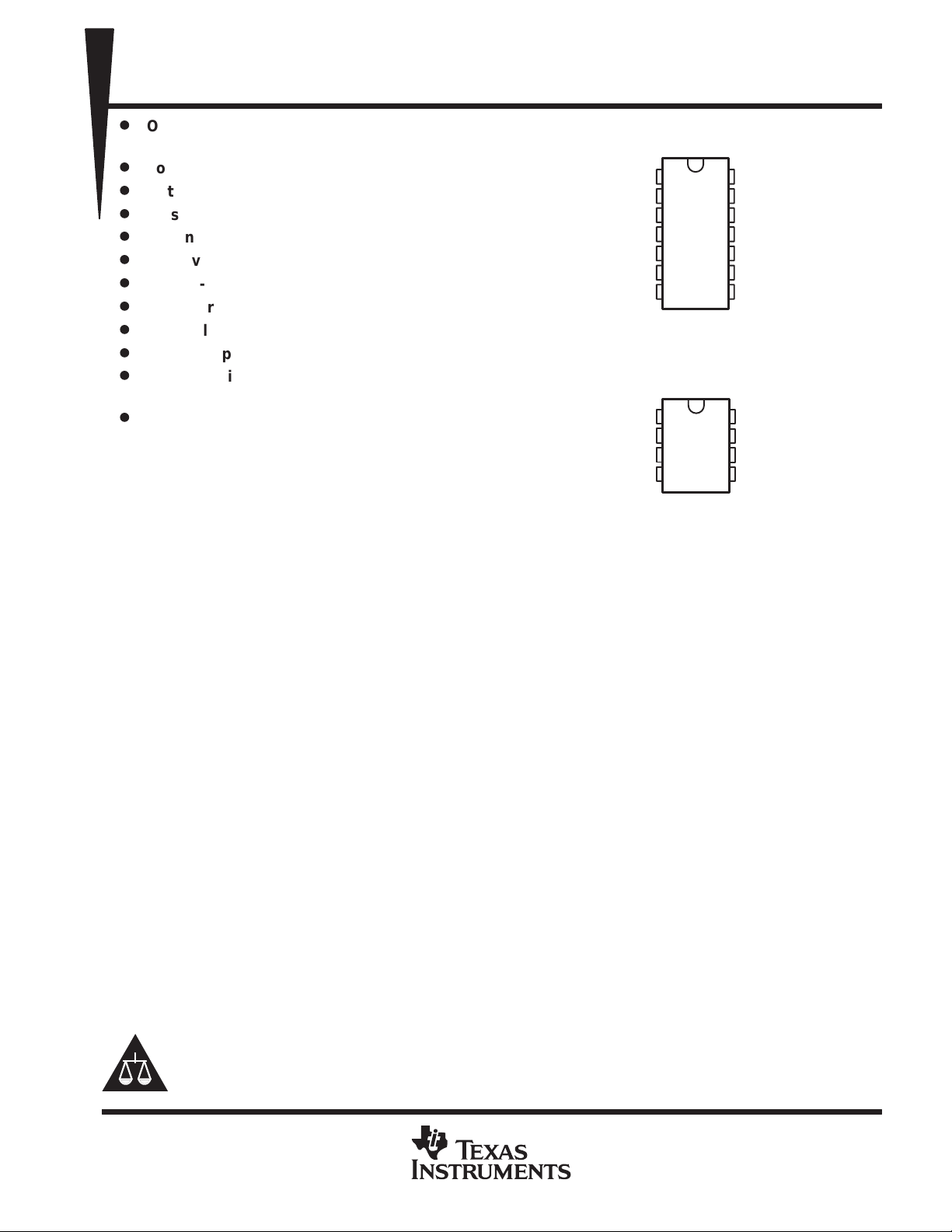
D PACKAGE
(TOP VIEW)
1
2
NC
3
VFB
4
NC
5
6
NC
RT/CT
7
D-8 OR P PACKAGE
(TOP VIEW)
REF
14
13
NC
12
V
CC
11
VC
10
OUTPUT
9
GND
8
POWER GROUND
Resistance
D
Designed to Be Interchangeable With
UC2842 and UC3842 Series
description
COMP
VFB
ISENSE
RT/CT
1
2
3
4
8
7
6
5
REF
V
CC
OUTPUT
GND
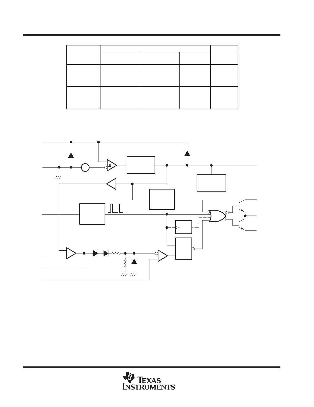
The TL284x and TL384x series of control
integrated circuits provide the features that are
necessary to implement off-line or dc-to-dc fixed-frequency current-mode control schemes with a minimum
number of external components. Some of the internally implemented circuits are an undervoltage lockout
(UVLO), featuring a start-up current of less than 1 mA, and a precision reference trimmed for accuracy at the
error amplifier input. Other internal circuits include logic to ensure latched operation, a pulse-width modulation
(PWM) comparator (which also provides current-limit control), and a totem-pole output stage designed to source
or sink high-peak current. The output stage, suitable for driving N-channel MOSFETs, is low when it is in the
off state.
Major differences between members of these series are the UVLO thresholds and maximum duty-cycle ranges.
Typical UVLO thresholds of 16 V (on) and 10 V (of f) on the TLx842 and TLx844 devices make them ideally suited
to off-line applications. The corresponding typical thresholds for the TLx843 and TLx845 devices are 8.4 V (on)
and 7.6 V (off). The TLx842 and TLx843 devices can operate to duty cycles approaching 100%. A duty-cycle
range of 0 to 50% is obtained by the TLx844 and TLx845 by the addition of an internal toggle flip-flop, which
blanks the output off every other clock cycle.
The TL284x-series devices are characterized for operation from –40°C to 85°C. The TL384x-series devices are
characterized for operation from 0°C to 70°C.
Please be aware that an important notice concerning availability, standard warranty, and use in critical applications of
Texas Instruments semiconductor products and disclaimers thereto appears at the end of this data sheet.
PRODUCTION DATA information is current as of publication date.
Products conform to specifications per the terms of Texas Instruments
standard warranty. Production processing does not necessarily include
testing of all parameters.
Copyright 1999, Texas Instruments Incorporated
POST OFFICE BOX 655303 • DALLAS, TEXAS 75265
1
TL284x, TL384x
CHIP FORM
CURRENT-MODE PWM CONTROLLERS
SLVS038E – JANUARY 1989 – REVISED DECEMBER 1999
T
A
0°C to 70°C
–40°C to 85°C
The D and D-8 packages are available taped and reeled. Add the suffix R to the device type (i.e.,
TL3842DR or TL3842DR-8).
functional block diagram
12
V
CC
SMALL OUTLINE
(D)
TL3842D
TL3843D
TL3844D
TL3845D
TL2842D
TL2843D
TL2844D
TL2845D
Chip forms are tested at 25°C.
AVAILABLE OPTIONS
PACKAGED DEVICES
SMALL OUTLINE
(D-8)
TL3842D-8
TL3843D-8
TL3844D-8
TL3845D-8
TL2842D-8
TL2843D-8
TL2844D-8
TL2845D-8
PLASTIC DIP
(P)
TL3842P
TL3843P
TL3844P
TL3845P
TL2842P
TL2843P
TL2844P
TL2845P
(Y)
TL3842Y
TL3843Y
TL3844Y
TL3845Y
–
–
–
–
34 V NOM
9
GND
VFB
7
3
1
5
RT/CT
COMP
ISENSE
†
The toggle flip-flop is present only in TL2844, TL2845, TL3844, and TL3845.
Pin numbers shown are for the D Package.
–
OSC
Error
Amplifier
+
–
UVLO
+
2R
5-V REF
EN
R1 V
Current-
Comparator
V
ref
Good
Logic
Sense
14
REF
Internal
Bias
11
VC
10
OUTPUT
†
T
S
R
PWM
Latch
8
POWER
GROUND
2
POST OFFICE BOX 655303 • DALLAS, TEXAS 75265
O
T
TL284x, TL384x
CURRENT-MODE PWM CONTROLLERS
SLVS038E – JANUARY 1989 – REVISED DECEMBER 1999
absolute maximum ratings over operating free-air temperature range (unless otherwise noted)
Supply voltage (see Note 1) (ICC < 30 mA) Self limiting. . . . . . . . . . . . . . . . . . . . . . . . . . . . . . . . . . . . . . . . . . . . . .
Analog input voltage range, VI (VFB and ISENSE) –0.3 V to 6.3 V. . . . . . . . . . . . . . . . . . . . . . . . . . . . . . . . . . . .
Output voltage, V
(OUTPUT) 35 V. . . . . . . . . . . . . . . . . . . . . . . . . . . . . . . . . . . . . . . . . . . . . . . . . . . . . . . . . . . . . . .
O
Input voltage, VI, (VC, D package only) 35 V. . . . . . . . . . . . . . . . . . . . . . . . . . . . . . . . . . . . . . . . . . . . . . . . . . . . . . .
Supply current, ICC 30 mA. . . . . . . . . . . . . . . . . . . . . . . . . . . . . . . . . . . . . . . . . . . . . . . . . . . . . . . . . . . . . . . . . . . . . .
Output current, IO ±1 A. . . . . . . . . . . . . . . . . . . . . . . . . . . . . . . . . . . . . . . . . . . . . . . . . . . . . . . . . . . . . . . . . . . . . . . . . .
Error amplifier output sink current 10 mA. . . . . . . . . . . . . . . . . . . . . . . . . . . . . . . . . . . . . . . . . . . . . . . . . . . . . . . . . .
Package thermal impedance, θ
(see Notes 2 and 3): D package 86°C/W. . . . . . . . . . . . . . . . . . . . . . . . . . . .
JA
D-8 package 97°C/W. . . . . . . . . . . . . . . . . . . . . . . . . .
P package 85°C/W. . . . . . . . . . . . . . . . . . . . . . . . . . . .
Virtual junction temperature range, T
0°C to 150°C. . . . . . . . . . . . . . . . . . . . . . . . . . . . . . . . . . . . . . . . . . . . . . . .
J
Output energy (capacitive load) 5 µJ. . . . . . . . . . . . . . . . . . . . . . . . . . . . . . . . . . . . . . . . . . . . . . . . . . . . . . . . . . . . . .
Lead temperature, 1,6 mm (1/16 inch) from case for 10 seconds 260°C. . . . . . . . . . . . . . . . . . . . . . . . . . . . . . .
Storage temperature range, T
†
Stresses beyond those listed under “absolute maximum ratings” may cause permanent damage to the device. These are stress ratings only, and
functional operation of the device at these or any other conditions beyond those indicated under “recommended operating conditions” is not
implied. Exposure to absolute-maximum-rated conditions for extended periods may affect device reliability.
NOTES: 1. All voltages are with respect to the device GND terminal.
2. Maximum power dissipation is a function of TJ(max),
ambient temperature is PD = (TJ(max) – TA)/
3. The package thermal impedance is calculated in accordance with JESD 51.
–65°C to 150°C. . . . . . . . . . . . . . . . . . . . . . . . . . . . . . . . . . . . . . . . . . . . . . . . . . .
stg
θ
, and TA. The maximum allowable power dissipation at any allowable
θ
JA
JA
. Operating at the absolute maximum TJ of 150°C can impact reliability.
recommended operating conditions
MIN NOM MAX UNIT
osc
O
O(ref)
‡
‡
CC
J
A
TL284x –40 85
TL384x
–0.1 1 V
100 500 kHz
0 125
0 70
Supply voltage, VCC and VC
Input voltage, VI, RT/CT 0 5.5 V
Input voltage, VI, VFB and ISENSE 0 5.5 V
Output voltage, VO, OUTPUT 0 30 V
Output voltage, VO, POWER GROUND
Supply current, externally limited, I
Average output current, I
Reference output current, I
Oscillator frequency, f
Operating virtual junction temperature, T
perating free-air temperature,
‡
These recommended voltages for VC and POWER GROUND apply only to the D package.
30 V
25 mA
200 mA
–20 mA
°C
°C
†
POST OFFICE BOX 655303 • DALLAS, TEXAS 75265
3
TL284x, TL384x
PARAMETER
TEST CONDITIONS
UNIT
PARAMETER
TEST CONDITIONS
UNIT
PARAMETER
TEST CONDITIONS
UNIT
CURRENT-MODE PWM CONTROLLERS
SLVS038E – JANUARY 1989 – REVISED DECEMBER 1999
electrical characteristics over recommended operating free-air temperature range, V
Note 4), R
= 10 kΩ, C
T
= 3.3 nF (unless otherwise specified)
T
= 15 V (see
CC
reference section
TL284x TL384x
MIN TYP†MAX MIN TYP†MAX
Output voltage IO = 1 mA, TA = 25°C 4.95 5 5.05 4.9 5 5.1 V
Line regulation VCC = 12 V to 25 V 6 20 6 20 mV
Load regulation IO = 1 mA to 20 mA 6 25 6 25 mV
Temperature coefficient
of output voltage
Output voltage
with worst-case variation
Output noise voltage f = 10 Hz to 10 kHz, TA = 25°C 50 50 µV
Output-voltage long-term drift After 1000 h at TA = 25°C 5 25 5 25 mV
Short-circuit output current –30 –100 –180 –30 –100 –180 mA
†
All typical values are at TA = 25°C.
NOTE 4: Adjust VCC above the start threshold before setting it to 15 V .
VCC = 12 V to 25 V, IO = 1 mA to 20 mA 4.9 5.1 4.82 5.18 V
0.2 0.4 0.2 0.4 mV/°C
oscillator section
TL284x TL384x
MIN TYP†MAX MIN TYP†MAX
Oscillator frequency (see Note 5) TA = 25°C 47 52 57 47 52 57 kHz
Frequency change with supply voltage VCC = 12 V to 25 V 2 10 2 10 Hz/kHz
Frequency change with temperature 50 50 Hz/kHz
Peak-to-peak amplitude at RT/CT 1.7 1.7 V
†
All typical values are at TA = 25°C.
NOTES: 4. Adjust VCC above the start threshold before setting it to 15 V .
5. Output frequency equals oscillator frequency for the TLx842 and TLx843. Output frequency is one-half oscillator frequency for the
TLx844 and TLx845.
error-amplifier section
TL284x TL384x
MIN TYP†MAX MIN TYP†MAX
Feedback input voltage COMP at 2.5 V 2.45 2.50 2.55 2.42 2.50 2.58 V
Input bias current –0.3 –1 –0.3 –2 µA
Open-loop voltage amplification VO = 2 V to 4 V 65 90 65 90 dB
Gain-bandwidth product 0.7 1 0.7 1 MHz
Supply-voltage rejection ratio VCC = 12 V to 25 V 60 70 60 70 dB
Output sink current VFB at 2.7 V, COMP at 1.1 V 2 6 2 6 mA
Output source current VFB at 2.3 V, COMP at 5 V –0.5 –0.8 –0.5 –0.8 mA
High-level output voltage VFB at 2.3 V, RL = 15 kΩ to GND 5 6 5 6 V
Low-level output voltage VFB at 2.7 V, RL = 15 kΩ to GND 0.7 1.1 0.7 1.1 V
†
All typical values are at TA = 25°C.
NOTE 4: Adjust VCC above the start threshold before setting it to 15 V .
4
POST OFFICE BOX 655303 • DALLAS, TEXAS 75265

PARAMETER
TEST CONDITIONS
UNIT
PARAMETER
TEST CONDITIONS
UNIT
High-level output voltage
V
Low-level output voltage
V
PARAMETER
UNIT
Start threshold voltage
V
Minimum operating voltage after startup
V
PARAMETER
UNIT
Maximum duty cycle
TL284x, TL384x
CURRENT-MODE PWM CONTROLLERS
SLVS038E – JANUARY 1989 – REVISED DECEMBER 1999
electrical characteristics over recommended operating free-air temperature range, V
Note 4), R
= 10 kΩ, C
T
= 3.3 nF (unless otherwise specified) (continued)
T
= 15 V (see
CC
current-sense section
TL284x TL384x
MIN TYP†MAX MIN TYP†MAX
Voltage amplification See Notes 6 and 7 2.85 3 3.13 2.85 3 3.15 V/V
Current-sense comparator threshold COMP at 5 V, See Note 6 0.9 1 1.1 0.9 1 1.1 V
Supply-voltage rejection ratio VCC = 12 V to 25 V, See Note 6 70 70 dB
Input bias current –2 –10 –2 –10 µA
Delay time to output 150 300 150 300 ns
†
All typical values are at TA = 25°C.
NOTES: 4. Adjust VCC above the start threshold before setting it to 15 V .
6. These parameters are measured at the trip point of the latch, with VFB at 0 V.
7. Voltage amplification is measured between ISENSE and COMP, with the input changing from 0 V to 0.8 V.
output section
TL284x TL384x
MIN TYP†MAX MIN TYP†MAX
p
p
Rise time CL = 1 nF, TA = 25°C 50 150 50 150 ns
Fall time CL = 1 nF, TA = 25°C 50 150 50 150 ns
†
All typical values are at TA = 25°C.
NOTE 4: Adjust VCC above the start threshold before setting it to 15 V .
IOH = –20 mA 13 13.5 13 13.5
IOH = –200 mA 12 13.5 12 13.5
IOL = 20 mA 0.1 0.4 0.1 0.4
IOL = 200 mA 1.5 2.2 1.5 2.2
undervoltage-lockout section
TL284x TL384x
MIN TYP†MAX MIN TYP†MAX
TLx842, TLx844 15 16 17 14.5 16 17.5
TLx843, TLx845 7.8 8.4 9 7.8 8.4 9
p
†
All typical values are at TA = 25°C.
NOTE 4: Adjust VCC above the start threshold before setting it to 15 V .
p
TLx842, TLx844 9 10 11 8.5 10 11.5
TLx843, TLx845 7 7.6 8.2 7 7.6 8.2
pulse-width-modulator section
TL284x TL384x
MIN TYP†MAX MIN TYP†MAX
TLx842, TLx843 95% 97% 100% 95% 97% 100%
TLx844, TLx845 46% 48% 50% 46% 48% 50%
Minimum duty cycle 0 0
†
All typical values are at TA = 25°C.
NOTE 4: Adjust VCC above the start threshold before setting it to 15 V .
POST OFFICE BOX 655303 • DALLAS, TEXAS 75265
5

TL284x, TL384x
PARAMETER
TEST CONDITIONS
UNIT
PARAMETER
TEST CONDITIONS
UNIT
PARAMETER
TEST CONDITIONS
UNIT
CURRENT-MODE PWM CONTROLLERS
SLVS038E – JANUARY 1989 – REVISED DECEMBER 1999
electrical characteristics over recommended operating free-air temperature range, V
Note 4), R
= 10 kΩ, C
T
= 3.3 nF (unless otherwise specified) (continued)
T
= 15 V (see
CC
supply voltage
TL284x TL384x
MIN TYP†MAX MIN TYP†MAX
Start-up current 0.5 1 0.5 1 mA
Operating supply current VFB and ISENSE at 0 V 11 17 11 17 mA
Limiting voltage ICC = 25 mA 34 34 V
†
All typical values are at TA = 25°C.
NOTE 4: Adjust VCC above the start threshold before setting it to 15 V .
electrical characteristics, V
= 15 V (see Note 4), RT = 10 kΩ, C
CC
= 3.3 nF , TA = 25°C (unless otherwise
T
specified)
reference section
TL384xY
MIN TYP MAX
Output voltage IO = 1 mA 5 V
Line regulation VCC = 12 V to 25 V 6 mV
Load regulation IO = 1 mA to 20 mA 6 mV
Temperature coefficient of output voltage 0.2 mV/°C
Output noise voltage f = 10 Hz to 10 kHz 50 µV
Output-voltage long-term drift After 1000 h at TA = 25°C 5 mV
Short-circuit output current –100 mA
NOTE 4: Adjust VCC above the start threshold before setting it to 15 V .
oscillator section
TL384xY
MIN TYP MAX
Oscillator frequency (see Note 5) 52 kHz
Frequency change with supply voltage VCC = 12 V to 25 V 2 Hz/kHz
Frequency change with temperature 5 Hz/kHz
Peak-to-peak amplitude at RT/CT 1.7 V
NOTES: 4. Adjust VCC above the start threshold before setting it to 15 V .
5. Output frequency equals oscillator frequency for the TLx842 and TLx843. Output frequency is one-half oscillator frequency for the
TLx844 and TLx845.
6
POST OFFICE BOX 655303 • DALLAS, TEXAS 75265
PARAMETER
TEST CONDITIONS
UNIT
PARAMETER
TEST CONDITIONS
UNIT
PARAMETER
TEST CONDITIONS
UNIT
High-level output voltage
V
Low-level output voltage
V
PARAMETER
UNIT
Start threshold voltage
V
Minimum operating voltage after startup
V
TL284x, TL384x
CURRENT-MODE PWM CONTROLLERS
SLVS038E – JANUARY 1989 – REVISED DECEMBER 1999
electrical characteristics, V
= 15 V (see Note 4), R
CC
= 10 kΩ, CT = 3.3 nF , TA= 25°C (unless otherwise
T
specified) (continued)
error-amplifier section
TL384xY
MIN TYP MAX
Feedback input voltage COMP at 2.5 V 2.50 V
Input bias current –0.3 µA
Open-loop voltage amplification VO = 2 V to 4 V 90 dB
Gain-bandwidth product 1 MHz
Supply-voltage rejection ratio VCC = 12 V to 25 V 70 dB
Output sink current VFB at 2.7 V, COMP at 1.1 V 6 mA
Output source current VFB at 2.3 V, COMP at 5 V –0.8 mA
High-level output voltage VFB at 2.3 V , RL = 15 kΩ to GND 6 V
Low-level output voltage VFB at 2.7 V, RL = 15 kΩ to GND 0.7 V
NOTE 4: Adjust VCC above the start threshold before setting it to 15 V .
current-sense section
TL384xY
MIN TYP MAX
Voltage amplification See Notes 6 and 7 3 V/V
Current-sense comparator threshold COMP at 5 V, See Note 6 1 V
Supply-voltage rejection ratio VCC = 12 V to 25 V, See Note 6 70 dB
Input bias current –2 µA
Delay time to output 150 ns
NOTES: 4. Adjust VCC above the start threshold before setting it to 15 V .
6. These parameters are measured at the trip point of the latch, with VFB at 0 V.
7. Voltage amplification is measured between ISENSE and COMP, with the input changing from 0 V to 0.8 V.
output section
TL384xY
MIN TYP MAX
p
p
Rise time CL = 1 nF 50 ns
Fall time CL = 1 nF 50 ns
NOTE 4: Adjust VCC above the start threshold before setting it to 15 V .
IOH = –20 mA 13.5
IOH = –200 mA 13.5
IOL = 20 mA 0.1
IOL = 200 mA 1.5
undervoltage-lockout section
TL384xY
MIN TYP MAX
TL3842Y, TL3844Y 16
TL3843Y, TL3845Y 8.4
p
NOTE 4: Adjust VCC above the start threshold before setting it to 15 V .
p
TL3842Y, TL3844Y 10
TL3843Y, TL3845Y 7.6
POST OFFICE BOX 655303 • DALLAS, TEXAS 75265
7

TL284x, TL384x
PARAMETER
UNIT
Maximum duty cycle
PARAMETER
TEST CONDITIONS
UNIT
CURRENT-MODE PWM CONTROLLERS
SLVS038E – JANUARY 1989 – REVISED DECEMBER 1999
electrical characteristics, V
= 15 V (see Note 4), R
CC
= 10 kΩ, CT = 3.3 nF , TA = 25°C (unless otherwise
T
specified) (continued)
pulse-width-modulator section
TL384xY
MIN TYP MAX
TL3842Y, TL3843Y 97%
TL3844Y, TL3845Y 48%
NOTE 4: Adjust VCC above the start threshold before setting it to 15 V .
supply voltage
TL384xY
MIN TYP MAX
Start-up current 0.5 1 mA
Operating supply current VFB and ISENSE at 0 V 11 17 mA
Limiting voltage ICC = 25 mA 34 V
NOTE 4: Adjust VCC above the start threshold before setting it to 15 V .
8
POST OFFICE BOX 655303 • DALLAS, TEXAS 75265
TL284x, TL384x
CURRENT-MODE PWM CONTROLLERS
SLVS038E – JANUARY 1989 – REVISED DECEMBER 1999
APPLICATION INFORMATION
Z
i
Z
f
NOTE A: Error amplifier can source or sink up to 0.5 mA.
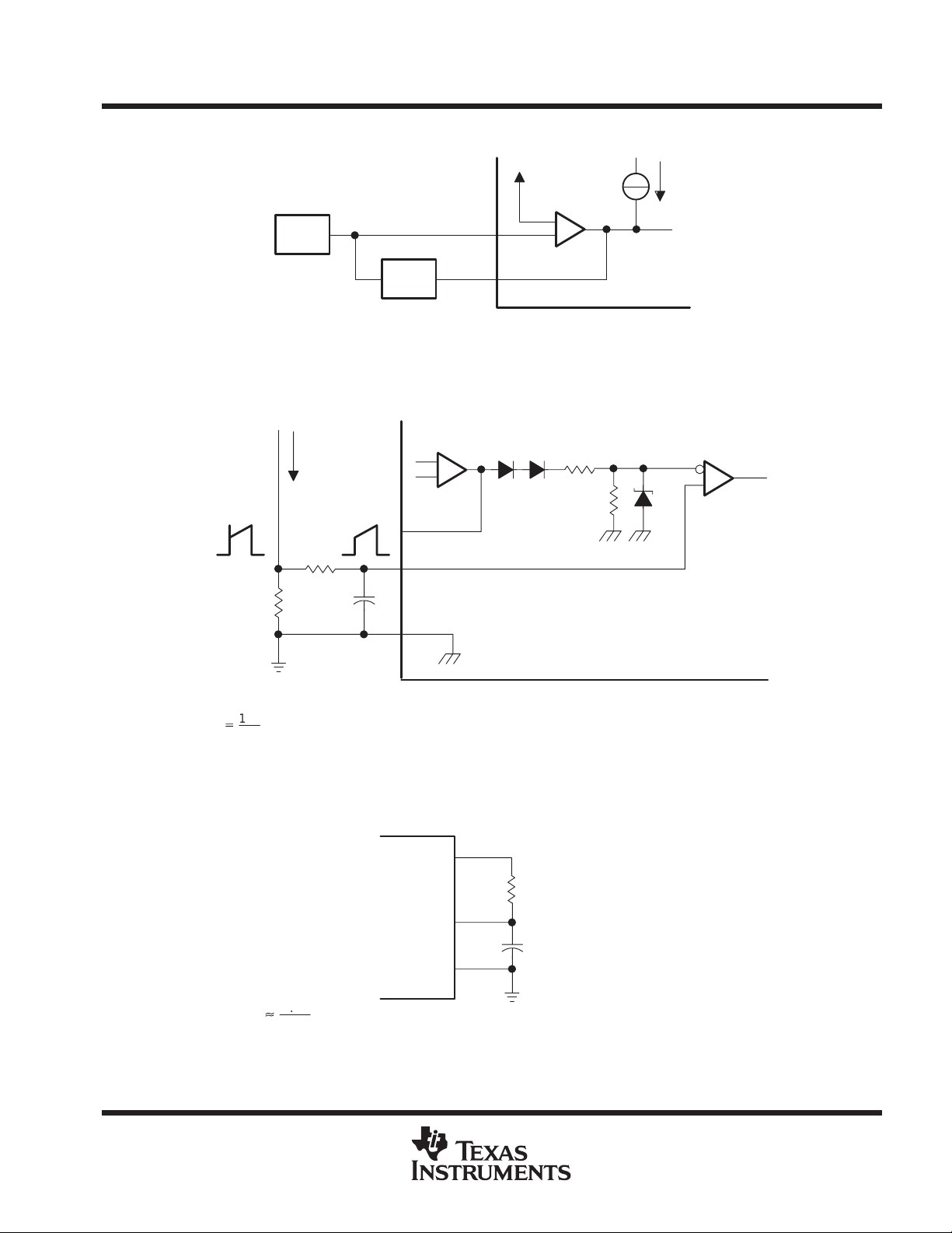
Figure 1. Error-Amplifier Configuration
I
S
(see Note A)
COMP
R
f
R
S
C
ISENSE
f
GND
VFB
COMP
Error
Amplifier
+
–
2.5 V
Error
Amplifier
+
–
2R
0.5 mA
R1 V
Current-Sense
Comparator
NOTE A: Peak current (IS) is determined by the formula:
I
S(max
A small RC filter formed by resistor Rf and capacitor Cf may be required to suppress switch transients.
1V
+
)
R
S
Figure 2. Current-Sense Circuit
NOTE A: For RT > 5 kΩ:
1.72
f
[
RTC
T
Figure 3. Oscillator Section
REF
RT/CT
GND
R
T
(see Note A)
C
T
POST OFFICE BOX 655303 • DALLAS, TEXAS 75265
9

TL284x, TL384x
CURRENT-MODE PWM CONTROLLERS
SLVS038E – JANUARY 1989 – REVISED DECEMBER 1999
APPLICATION INFORMATION
100
40
sµ
10
Dead Time –
0.4
0.1
VCC = 15 V
RT ≥ 5 kΩ
TA = 25°C
4
1
DEAD TIME
vs
TIMING CAPACITANCE
CT – Timing Capacitance – nF
Figure 4
TIMING RESISTANCE
vs
FREQUENCY
100
40
Ω
CT = 22 nF
10
CT = 47 nF
– Timing Resistance – k
4
T
R
1
100401040
100 1 k 10 k 100 k 1 M
CT = 100 nF
VCC = 15 V
TA = 25°C
f - Frequency - Hz
CT = 10 nF
CT = 4.7 nF
CT = 22 nF
CT = 1 nF
Figure 5
open-loop laboratory test fixture
In the open-loop laboratory test fixture shown in Figure 6, high peak currents associated with loads necessitate
careful grounding techniques. Timing and bypass capacitors should be connected close to the GND terminal
in a single-point ground. The transistor and 5-kΩ potentiometer sample the oscillator waveform and apply an
adjustable ramp to the ISENSE terminal.
R
Error Amplifier
1 kΩ
Adjust
4.7 kΩ
4.7 kΩ
2N2222
100 kΩ
5 kΩ
ISENSE
Adjust
T
COMP
VFB
ISENSE
RT/CT
DUT
TL284x
TL384x
C
T
REF
V
CC
OUTPUT
GND
0.1 µF
Figure 6. Open-Loop Laboratory Test Fixture
A
0.1 µF
1 kΩ, 1 W
REF
V
CC
OUTPUT
GND
10
POST OFFICE BOX 655303 • DALLAS, TEXAS 75265

TL284x, TL384x
CURRENT-MODE PWM CONTROLLERS
SLVS038E – JANUARY 1989 – REVISED DECEMBER 1999
APPLICATION INFORMATION
shutdown technique
The PWM controller (see Figure 7) can be shut down by two methods: either raise the voltage at ISENSE above
1 V or pull the COMP terminal below a voltage two diode drops above ground. Either method causes the output
of the PWM comparator to be high (refer to block diagram). The PWM latch is reset dominant so that the output
remains low until the next clock cycle after the shutdown condition at the COMP or ISENSE terminal is removed.
In one example, an externally latched shutdown can be accomplished by adding an SCR that resets by cycling
V
below the lower UVLO threshold. At this point, the reference turns off, allowing the SCR to reset.
CC
Shutdown
1 kΩ
330 Ω
500 Ω
REF
COMP
Shutdown
ISENSE
To Current-Sense
Resistor
Figure 7. Shutdown Techniques
A fraction of the oscillator ramp can be resistively summed with the current-sense signal to provide slope
compensation for converters requiring duty cycles over 50% (see Figure 8). Note that capacitor C forms a filter
with R2 to suppress the leading-edge switch spikes.
REF
0.1 µF
RT/CT
R
T
ISENSE
C
T
R1
R2
C
Figure 8. Slope Compensation
POST OFFICE BOX 655303 • DALLAS, TEXAS 75265
ISENSE
R
SENSE
11

IMPORTANT NOTICE
T exas Instruments and its subsidiaries (TI) reserve the right to make changes to their products or to discontinue
any product or service without notice, and advise customers to obtain the latest version of relevant information
to verify, before placing orders, that information being relied on is current and complete. All products are sold
subject to the terms and conditions of sale supplied at the time of order acknowledgement, including those
pertaining to warranty, patent infringement, and limitation of liability.
TI warrants performance of its semiconductor products to the specifications applicable at the time of sale in
accordance with TI’s standard warranty. Testing and other quality control techniques are utilized to the extent
TI deems necessary to support this warranty . Specific testing of all parameters of each device is not necessarily
performed, except those mandated by government requirements.
CERTAIN APPLICATIONS USING SEMICONDUCTOR PRODUCTS MAY INVOLVE POTENTIAL RISKS OF
DEATH, PERSONAL INJURY, OR SEVERE PROPERTY OR ENVIRONMENTAL DAMAGE (“CRITICAL
APPLICATIONS”). TI SEMICONDUCTOR PRODUCTS ARE NOT DESIGNED, AUTHORIZED, OR
WARRANTED TO BE SUITABLE FOR USE IN LIFE-SUPPORT DEVICES OR SYSTEMS OR OTHER
CRITICAL APPLICA TIONS. INCLUSION OF TI PRODUCTS IN SUCH APPLICATIONS IS UNDERST OOD TO
BE FULLY AT THE CUSTOMER’S RISK.
In order to minimize risks associated with the customer’s applications, adequate design and operating
safeguards must be provided by the customer to minimize inherent or procedural hazards.
TI assumes no liability for applications assistance or customer product design. TI does not warrant or represent
that any license, either express or implied, is granted under any patent right, copyright, mask work right, or other
intellectual property right of TI covering or relating to any combination, machine, or process in which such
semiconductor products or services might be or are used. TI’s publication of information regarding any third
party’s products or services does not constitute TI’s approval, warranty or endorsement thereof.
Copyright 1999, Texas Instruments Incorporated
 Loading...