

查询TL080CPW供应商
TL080, TL081, TL082, TL084, TL081A, TL082A, TL084A
TL081B, TL082B, TL084B, TL082Y, TL084Y
JFET-INPUT OPERATIONAL AMPLIFIERS
SLOS081A–D2297, FEBRUARY 1977–REVISED NOVEMBER 1992
24 DEVICES COVER COMMERCIAL, INDUSTRIAL, AND MILITARY TEMPERATURE RANGES
• Low-Power Consumption
• Wide Common-Mode and Differential
Voltage Ranges
• Low Input Bias and Offset Currents
• Output Short-Circuit Protection
• Low Total Harmonic
Distortion . . . 0.003% Typ
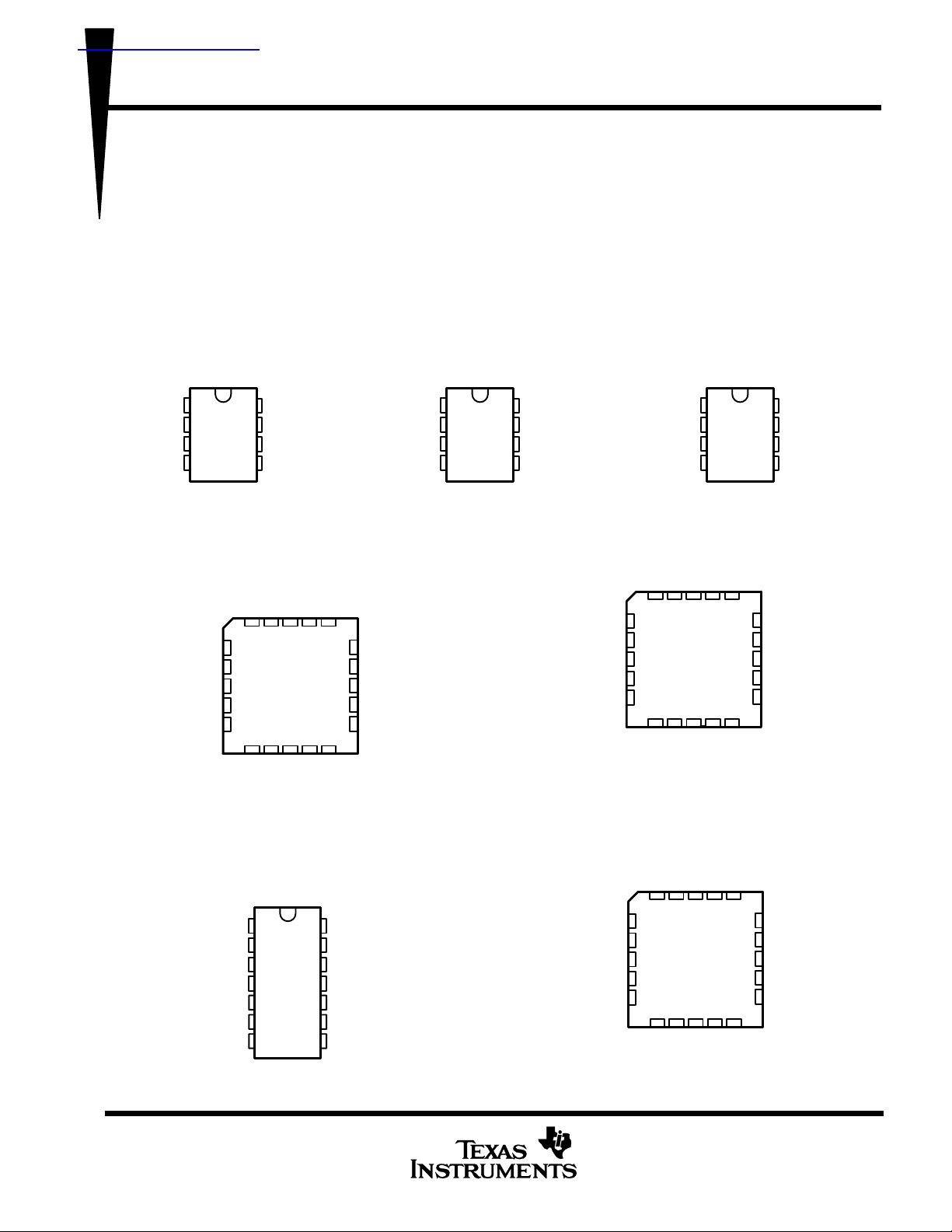
D, P, OR PW PACKAGE
N1/COMP
IN–
IN+
V
CC–
NC–No internal connection
TL080
(TOP VIEW)
1
2
3
4
NC
IN–
NC
IN+
NC
D, J, N, OR PW PACKAGE
1 OUT
1 IN–
1 IN+
V
CC+
2 IN+
2 IN–
2 OUT
COMP
8
V
7
CC+
OUT
6
OFFSET N2
5
TL081M . . . FK PACKAGE
(TOP VIEW)
NC
OFFSET N1
NC
3212019
4
5
6
7
8
910111213
NC
NC
CC–
V
TL084, TL084A, TL084B
(TOP VIEW)
1
14
2
13
3
12
4
11
5
10
6
7
NC
OFFSET N2
9
8
OFFSET N1
NC
NC
18
V
17
NC
16
OUT
15
NC
14
NC
4 OUT
4 IN–
4 IN+
V
CC–
3 IN+
3 IN–
3 OUT
TL081, TL081A, TL081B
D, JG, P, OR PW PACKAGE
(TOP VIEW)
1
IN–
2
IN+
3
CC+
V
CC–
4
• High Input Impedance . . . JFET-Input Stage
• Internal Frequency Compensation (Except
TL080, TL080A)
• Latch-Up-Free Operation
• High Slew Rate . . . 13 V/µs Typ
• Common-Mode Input Voltage Range
NC
8
V
7
CC+
OUT
6
OFFSET N2
5
Includes V
NC
1 IN–
NC
1 IN+
NC
1 IN+
NC
V
CC+
NC
2 IN+
CC+
TL082, TL082A, TL082B
D, JG, P, OR PW PACKAGE
(TOP VIEW)
1 OUT
1 IN–
1 IN+
V
CC–
TL082M ...FK PACKAGE
NC
3 2 1 20 19
4
5
6
7
8
910111213
NC
TL084M ...FK PACKAGE
1 IN–
3212019
4
5
6
7
8
910111213
1
2
3
4
(TOP VIEW)
CC+
V
1 OUT
NC
NC
CC–
2 IN+
V
(TOP VIEW)
1 OUT
NC
4 OUT
NC
18
17
16
15
14
NC
4 IN–
18
17
16
15
14
NC
2 IN–
2 OUT
3 IN–
3 OUT
8
7
6
5
NC
2 OUT
NC
2 IN–
NC
4 IN+
NC
VCC–
NC
3 IN+
V
CC+
2 OUT
2 IN–
2 IN+
PRODUCTION DATA information is current as of publication date.
Products conform to specifications per the terms of Texas Instruments
standard warranty. Production processing does not necessarily include
testing of all parameters.
POST OFFICE BOX 655303 • DALLAS, TEXAS 75265
POST OFFICE BOX 1443
• HOUSTON, TEXAS
77251–1443
Copyright 1992, Texas Instruments Incorporated
On products compliant to MIL-STD-883, Class B, all parameters are
tested unless otherwise noted. On all other products, production
processing does not necessarily include testing of all parameters.
1
TL080, TL081, TL082, TL084, TL081A, TL082A, TL084A
IO
CHIP
TL081B, TL082B, TL084B, TL082Y, TL084Y
JFET-INPUT OPERATIONAL AMPLIFIERS
SLOS081A–D2297, FEBRUARY 1977–REVISED NOVEMBER 1992
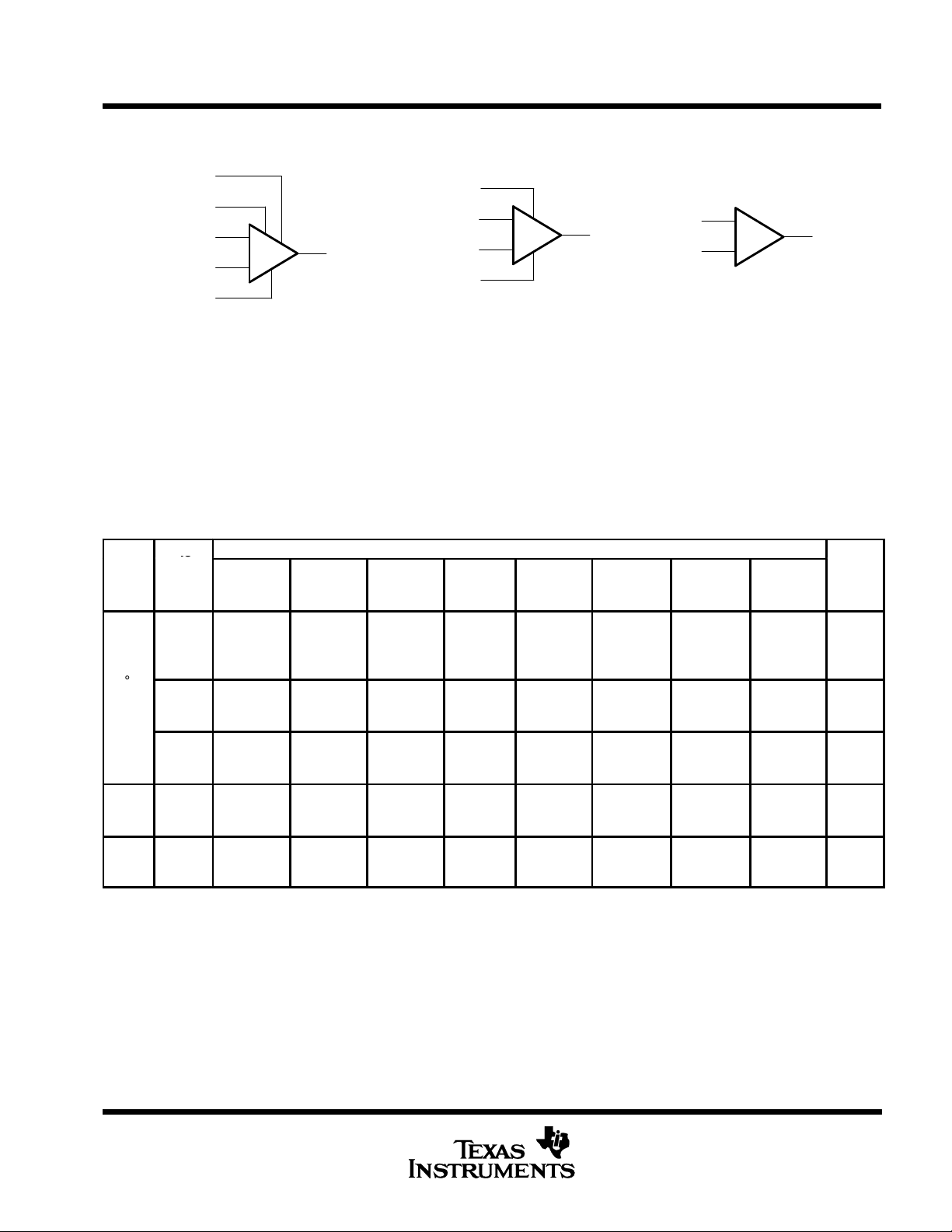
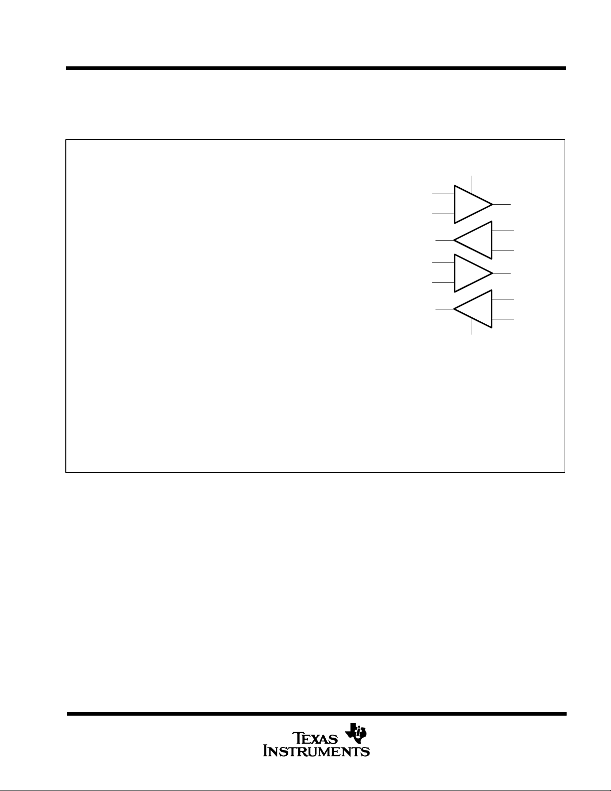
symbols
N1/COMP
COMP
IN+
IN–
OFFSET N2
TL080
TL081
OFFSET N1
IN+
+
–
OUT
IN–
OFFSET N2
+
–
OUT
TL082 (each amplifier)
TL084 (each amplifier)
IN+
IN–
+
–
description
The TL08_ JFET-input operational amplifier family is designed to offer a wider selection than any previously
developed operational amplifier family. Each of these JFET-input operational amplifiers incorporates
well-matched, high-voltage JFET and bipolar transistors in a monolithic integrated circuit. The devices feature
high slew rates, low input bias and offset currents, and low offset voltage temperature coefficient. Offset
adjustment and external compensation options are available within the TL08_ family.
Device types with a C suffix are characterized for operation from 0°C to 70°C, those with an I suffix are
characterized for operation from –40°C to 85°C, and those with an M suffix are characterized for operation over
the full military temperature range of –55°C to 125°C.
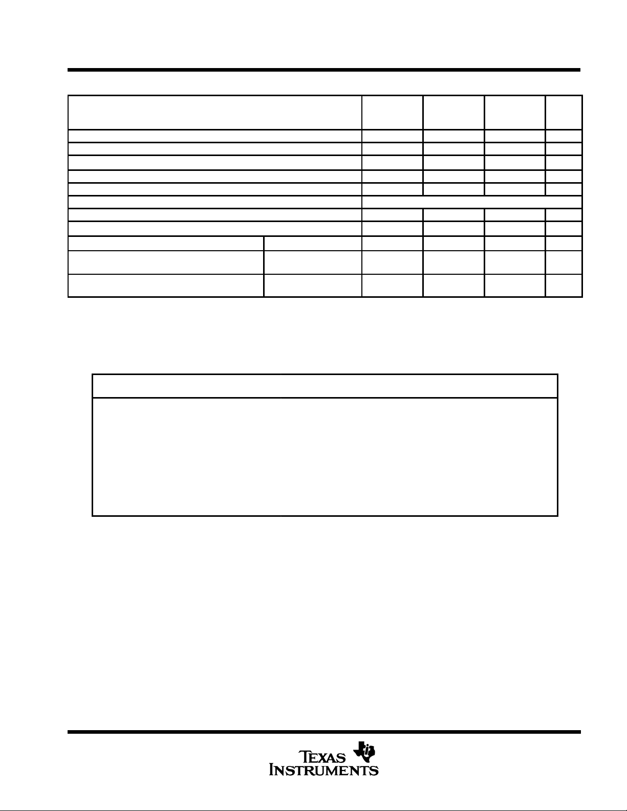
AVAILABLE OPTIONS
V
IO
T
0°C
to
70°C
–40°C
85°C
–55°C
to
125°C
The D package is available taped and reeled. Add R suffix to device type, (e.g., TL080CDR).
MAX
A
to
at
25°C
15 mV
15 mV
6 mV
3 mV
15 mV
6 mV
3 mV
15 mV
6 mV
3 mV
6 mV
6 mV
6 mV
6 mV
6 mV
9 mV
SMALL
OUTLINE
(D008)
TL080CD
TL081CD
TL081ACD
TL081BCD
TL082CD
TL082ACD
TL082BCD
—
TL081ID
TL082ID
TL084ID
— —
SMALL
OUTLINE
(D014)
— — — — —
— — — — —
TL084CD
TL084ACD
TL084BCD
TL084ID
CHIP
CARRIER
(FK)
— — —
— — —
TL081MFK
TL082MFK
TL084MFK
PACKAGE
CERAMIC
DIP
(J)
TL084MJ
CERAMIC
DIP
(JG)
TL081MJG
TL082MJG
PLASTIC
DIP
(N)
TL084CN
TL084ACN
TL084BCN
TL084IN
— — — —
PLASTIC
DIP
(P)
TL080CP
TL081CP
TL081ACP
TL081BCP
TL082CP
TL082ACP
TL082BCP
—
TL081IP
TL082IP
TSSOP
(PW)
TL080CPW
TL081CPW
TL082CPW TL082Y
TL084CPW TL084Y
— —
OUT
FORM
(Y)
—
2
POST OFFICE BOX 655303 • DALLAS, TEXAS 75265
POST OFFICE BOX 1443
• HOUSTON, TEXAS
77251–1443
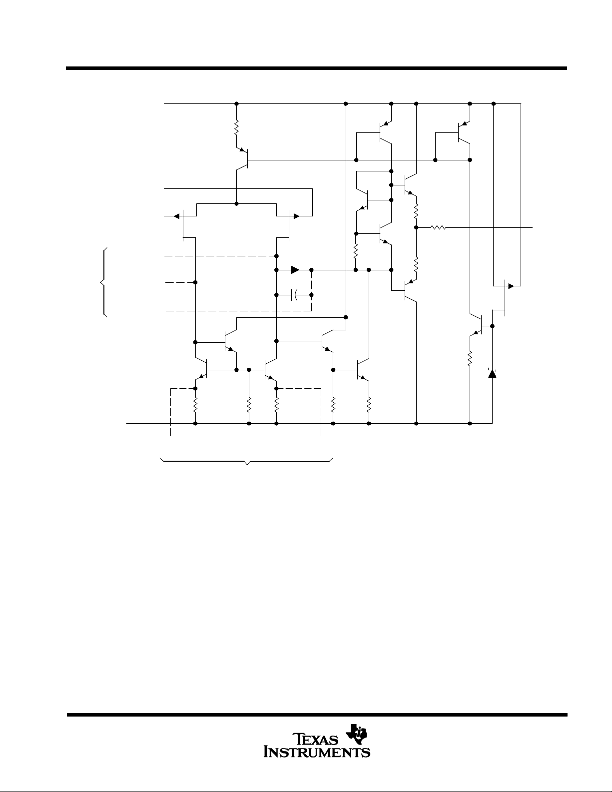
schematic (each amplifier)
V
CC+
IN+
TL080, TL081, TL082, TL084, TL081A, TL082A, TL084A
TL081B, TL082B, TL084B
JFET-INPUT OPERATIONAL AMPLIFIERS
SLOS081A–D2297, FEBRUARY 1977–REVISED NOVEMBER 1992
IN–
N1/COMP
TL080
Only
C1 = 18 pF on TL081, TL082, and TL084 only (including their suffix versions).
Component values shown are nominal.
V
CC–
OFFSET N2
COMP
1080 Ω
OFFSET N1
TL081 Only
C1
1080 Ω
OFFSET N2
64 Ω
OUT
128 Ω
64 Ω
POST OFFICE BOX 655303 • DALLAS, TEXAS 75265
POST OFFICE BOX 1443
• HOUSTON, TEXAS
77251–1443
3
TL082Y
JFET-INPUT DUAL OPERATIONAL AMPLIFIER
SLOS081A–D2297, FEBRUARY 1977–REVISED NOVEMBER 1992
chip information
These chips, when properly assembled, display characteristics similar to the TL082. Thermal compression or
ultrasonic bonding may be used on the doped aluminum bonding pads. Chips may be mounted with conductive
epoxy or a gold-silicon preform.
BONDING PAD ASSIGNMENTS
V
CC+
(8)
+
–
V
CC–
(4)
(1)
(5)
+
(6)
–
1 IN+
1 IN–
1 OUT
(3)
(2)
(7)
2 OUT
2 IN+
2 IN–
CHIP THICKNESS: 15 TYPICAL
BONDING PADS: 4 × 4 MINIMUM
TJmax = 150°C
TOLERANCES ARE ±10%
ALL DIMENSIONS ARE IN MILS
PIN (4) INTERNALLY CONNECTED
TO BACKSIDE OF CHIP
4
POST OFFICE BOX 655303 • DALLAS, TEXAS 75265
POST OFFICE BOX 1443
• HOUSTON, TEXAS
77251–1443
JFET-INPUT QUAD OPERATIONAL AMPLIFIER
SLOS081A–D2297, FEBRUARY 1977–REVISED NOVEMBER 1992
chip information
These chips, when properly assembled, display characteristics similar to the TL084. Thermal compression or
ultrasonic bonding may be used on the doped aluminum bonding pads. Chips may be mounted with conductive
epoxy or a gold-silicon preform.
BONDING PAD ASSIGNMENTS
V
CC+
(4)
+
–
+
–
V
CC–
(11)
(1)
(5)
+
(6)
–
(8)
(12)
+
(13)
–
1 IN+
1 IN–
2 OUT
3 IN+
3 IN–
4 OUT
(3)
(2)
(7)
(10)
(9)
(14)
TL084Y
1 OUT
2 IN+
2 IN–
3 OUT
4 IN+
4 IN–
CHIP THICKNESS: 15 TYPICAL
BONDING PADS: 4 × 4 MINIMUM
TJmax = 150°C
TOLERANCES ARE ±10%
ALL DIMENSIONS ARE IN MILS
PIN (11) INTERNALLY CONNECTED
TO BACKSIDE OF CHIP
POST OFFICE BOX 655303 • DALLAS, TEXAS 75265
POST OFFICE BOX 1443
• HOUSTON, TEXAS
77251–1443
5
TL080, TL081, TL082, TL084, TL081A, TL082A, TL084A
TL081B, TL082B, TL084B
JFET-INPUT OPERATIONAL AMPLIFIERS
SLOS081A–D2297, FEBRUARY 1977–REVISED NOVEMBER 1992
absolute maximum ratings over operating free-air temperature range (unless otherwise noted)
TL08_C
TL08_AC
TL08_BC
Supply voltage, V
Supply voltage VCC– (see Note 1) –18 –18 –18 V
Differential input voltage (see Note 2)
Input voltage (see Notes 1 and 3) ±15 ±15 ±15 V
Duration of output short circuit (see Note 4) unlimited unlimited unlimited
Continuous total dissipation See Dissipation Rating Table
Operating free-air temperature range 0 to 70 – 40 to 85 – 55 to 125 °C
Storage temperature range – 65 to 150 – 65 to 150 – 65 to 150
Case temperature for 60 seconds FK package 260
Lead temperature 1,6 mm (1/16 inch)
from case for 60 seconds
Lead temperature 1,6 mm (1/16 inch)
from case for 10 seconds
NOTES: 1. All voltage values, except differential voltages, are with respect to the midpoint between V
2. Differential voltages are at the noninverting input terminal with respect to the inverting input terminal.
3. The magnitude of the input voltage must never exceed the magnitude of the supply voltage or 15 V, whichever is less.
4. The output may be shorted to ground or to either supply. Temperature and/or supply voltages must be limited to ensure that the
dissipation rating is not exceeded.
(see Note 1) 18 18 18 V
CC+
± 30
J or JG package 300 °C
D, N, P, or PW package 260 260 °C
TL08_I TL08_M UNIT
± 30 ± 30 V
°C
°C
CC+
and V
CC–
.
DISSIPATION RATING TABLE
PACKAGE
D (8 Pin) 680 mW 5.8 mW/°C 32°C 464 mW 377 mW N/A
D (14 Pin) 680 mW
FK 680 mW 11.0 mW/°C88°C 680 mW 680 mW 275 mW
J 680 mW 11.0 mW/°C88°C 680 mW 680 mW 275 mW
JG 680 mW 8.4 mW/°C69°C 672 mW 546 mW 210 mW
N 680 mW 9.2 mW/°C76°C 680 mW 598 mW N/A
P 680 mW
PW (8 Pin) 525 mW
PW (14 Pin) 700 mW 5.6 mW/°C 25°C 448 mW N/A N/A
TA ≤ 25°C
POWER RATING
DERATING
FACTOR
7.6 mW/ °C
8.0 mW/°C
4.2 mW/°C
DERATE
ABOVE T
60°C 608 mW 494 mW N/A
65°C 640 mW 520 mW N/A
25°C 336 mW N/A N/A
TA = 70°C
POWER RATING
A
TA = 85°C
POWER RATING
POWER RATING
TA = 125°C
6
POST OFFICE BOX 655303 • DALLAS, TEXAS 75265
POST OFFICE BOX 1443
• HOUSTON, TEXAS
77251–1443

TL080, TL081, TL084, TL081A, TL082A, TL084A
†
VIOInput offset voltage
mV
VIOInput
offset
voltage
mV
IIOInput offset current
‡
V
O
=0
IIOInput
offset
current
‡
V
0
IIBInput bias current
‡
V
O
=0
IIBInput
bias
current
‡
V
0
V
Maximum peak
V
M
i
k
output voltage swing
T
A
= full range
OM
output
voltage
swing
T
full
range
A
VD
V/mV
A
V/mV
CMRR
7086808680
868086
dB
CMRR
7086808680
868086
dB
k
SVR
7086808680
868086
dB
k
7086808680
868086
dB
TL081B, TL082B, TL084B
JFET-INPUT OPERATIONAL AMPLIFIERS
SLOS081A–D2297, FEBRUARY 1977–REVISED NOVEMBER 1992
UNIT
TL081I
TL082I
TL084I
TL082BC
TL084BC
TLO81BC
TL081AC
TL082AC
TL084AC
V
to
15
–12
±11
to
15
–12
±11
to
15
–12
±11
12
12
12
Ω
10
10
10
is 0°C to 70°C for TL08_C, TL08_AC,
A
18 18 18 18 µV/°C
TL080C
TL081C
TL082C
TL084C
MIN TYP MAX MIN TYP MAX MIN TYP MAX MIN TYP MAX
= 50 Ω,
= 25°C 3 15 3 6 2 3 3 6
= full range 20 7.5 5 9
A
A
T
= ±15 V (unless otherwise noted)
CC±
PARAMETER TEST CONDITIONS
= 0,
= 50 Ω T
S
O
V
R
= 25°C 5 200 5 100 5 100 5 100 pA
S
R
T
= 0,
= full range
O
A
V
T
Temperature coefficient
of input offset voltage
= full range 2 2 2 10 nA
= 25°C 30 400 30 200 30 200 30 200 pA
A
A
T
T
=
O
= full range 10 7 7 20 nA
A
A
T
=
O
to
15
–12
= 10 kΩ ±12 ±13.5 ±12 ±13.5 ±12 ±13.5 ±12 ±13.5
L
= 25°C ±11
= 25°C R
A
A
T
T
mum pea
Common-mode
ax
input voltage range
12
25 200 50 200 50 200 50 200
15 25 25 25
= 0,
= 25°C 3 3 3 3 MHz
A
Unity-gain bandwidth T
= 25°C 10
Input resistance T
A
= 0,
= 25°C
O
A
T
min, V
ICR
= ±15 V to ± 9 V, V
= V
= 50 Ω,
S
IC
V
R
V
Common-mode
rejection ratio
≥ 10 kΩ ±12 ±12 ±12 ±12 V
≥ 2 kΩ ±10 ±12 ±10 ±12 ±10 ±12 ±10 ±12
≥ 2 k Ω,
L
L
R
R
=
A
≥ 2 kΩ,
L
L
R
R
= ±10 V,
= ±10 V,
= 25°C
O
V
= full range
O
A
A
T
V
T
Large-signal differential
voltage amplification
1.4 2.8 1.4 2.8 1.4 2.8 1.4 2.8 mA
O
= 0,
= 25°C
A
T
= 50 Ω,
S
CC
R
)
IO
/ ∆V
CC±
Supply voltage rejection
ratio (∆V
= 25°C 120 120 120 120 dB
O
A
V
= 100, T
= 25°C
VD
A
No load,
T
Supply current
(per amplifier)
Crosstalk attenuation A
VIO
electrical characteristics, V
α
ICR
V
POST OFFICE BOX 1443 HOUSTON, TEXAS 77001POST OFFICE BOX 655303 DALLAS, TEXAS 75265
OM
V
•• 7
VD
1
i
B
r
SVR
CC
I
02
/V
01
TL08_BC and –40°C to 85°C for TL08_I.
Input bias currents of a FET-input operational amplifier are normal junction reverse currents, which are temperature sensitive as shown in Figure 18. Pulse techniques must be used
that will maintain the junction temperature as close to the ambient temperature as possible.
All characteristics are measured under open-loop conditions with zero common-mode voltage unless otherwise specified. Full range for T
V
‡
†

TL081M, TL082M, TL084M
PARAMETER
TEST CONDITIONS
†
UNIT
VIOI
V
0
R
50 Ω
V
IIOI
t
‡
V
0
IIBI
t
‡
V
0
Maximum peak
OM
T
55°C to 125°C
A
diff
V/mV
SR
Sl
V/
VnEquivalent i
R
100 Ω
JFET-INPUT OPERATIONAL AMPLIFIERS
SLOS081A–D2297, FEBRUARY 1977–REVISED NOVEMBER 1992
electrical characteristics, V
nput offset voltage
Temperature
α
VIO
V
ICR
V
OM
VD
B
1
r
i
CMRR
k
SVR
I
CC
V01/V
†
All characteristics are measured under open-loop conditions with zero common-mode input voltage unless otherwise specified.
‡
Input bias currents of a FET-input operational amplifier are normal junction reverse currents, which are temperature sensitive as shown in
Figure 18. Pulse techniques must be used that will maintain the junction temperatures as close to the ambient temperature as is possible.
coefficient of input
offset voltage
nput offset curren
nput bias curren
Common-mode
input voltage range
Maximum peak
output voltage
swing
Large-signal
erential voltage
amplification
Unity-gain
bandwidth
Input resistance TA = 25°C 10
Common-mode
rejection ratio
Supply voltage
rejection ratio
(∆V
Supply current
(per amplifier)
Crosstalk
02
attenuation
CC±
/∆VIO)
=
O
VO = 0,
TA = –55°C to 125°C
=
O
=
O
TA = 25°C ±11
TA = 25°C, RL = 10 kΩ ±12 ±13.5 ±12 ±13.5
= –
A
VO = ±10 V,
TA = 25°C
VO = ±10 V,
TA = –55°C to 125°C
TA = 25°C 3 3 MHz
VIC = V
RS = 50 Ω,
VCC = ±15 V to ±9 V,
RS = 50 Ω,
No load, VO = 0, TA = 25°C 1.4 2.8 1.4 2.8 mA
AVD = 100, TA = 25°C 120 120 dB
= ±15 V (unless otherwise noted)
CC ±
,
°
ICR
=
S
min,
TA = 25°C 3 6 3 9
TA = –55°C to 125°C 9 15
RS= 50 Ω,
TA = 25°C 5 100 5 100 pA
TA = 125°C 20 20 nA
TA = 25°C 30 200 30 200 pA
TA = 125°C 50 50 nA
RL ≥ 10 kΩ ±12 ±12 V
°
RL ≥ 2 kΩ ±10 ±12 ±10 ±12
RL ≥ 2 kΩ,
RL ≥ 2 kΩ,
VO = 0,
TA = 25°C
VO = 0,
TA = 25°C
TL081M, TL082M TL084M
MIN TYP MAX MIN TYP MAX
18 18 µV/°C
±12
to
15
25 200 25 200
15 15
12
80 86 80 86 dB
80 86 80 86 dB
±11
± 12
10
to
15
12
m
V
Ω
operating characteristics, V
PARAMETER TEST CONDITIONS MIN TYP MAX
ew rate at unity gain
t
Rise time VI = 20 mV, RL = 2 kΩ, 0.05 µs
r
Overshoot factor CL = 100 pF, See Figure 1 20%
nput noise voltage
I
Equivalent input noise current RS = 100 Ω, f = 1 kHz 0.01 pA/√Hz
n
THD Total harmonic distortion
∗On products compliant to MIL-STD-883, Class B, this parameter is not production tested.
8
= ±15 V, T
CC±
= 25°C (unless otherwise noted)
A
VI = 10 V,
CL = 100 pF,
VI = 10 V, RL = 2 kΩ,
TA = – 55°C to 125°C,
=
S
V
= 10 V,
O(rms)
f = 1 kHz
POST OFFICE BOX 655303 • DALLAS, TEXAS 75265
POST OFFICE BOX 1443
RL = 2 kΩ,
See Figure 1
f = 1 kHz 18 nV/√Hz
f = 10 Hz to 10 kHz 4 µV
RS ≤ 1 kΩ, RL ≥ 2 kΩ,
• HOUSTON, TEXAS 77001
CL = 100 pF,
See Figure 1
UNIT
∗
8
∗
5
13
µs
0.003%

TL080, TL081, TL084, TL081A, TL082A, TL084A
CMRR
Common-mode rejection ratio
7086dB
k
Supply voltage rejection ratio (∆V
/ ∆VIO)
7086dB
VnEquivalent i
R
100 Ω
TL081B, TL082B, TL084B
JFET-INPUT OPERATIONAL AMPLIFIERS
SLOS081A–D2297, FEBRUARY 1977–REVISED NOVEMBER 1992
TL082Y, TL084Y electrical characteristics, V
PARAMETER TEST CONDITIONS
V
IO
α
VIO
I
IO
I
IB
V
ICR
V
OM
A
VD
B
1
r
i
SVR
I
CC
V01/V02Crosstalk attenuation AVD = 100, TA = 25°C 120 dB
†
All characteristics are measured under open-loop conditions with zero common-mode voltage unless otherwise specified.
‡
Input bias currents of a FET-input operational amplifier are normal junction reverse currents, which are temperature sensitive as shown in
Figure 18. Pulse techniques must be used that will maintain the junction temperature as close to the ambient temperature as possible.
operating characteristics, V
SR Slew rate at unity gain
t
r
I
n
THD Total harmonic distortion
Input offset voltage
Temperature coefficient of input offset voltage VO = 0, RS = 50 Ω, TA = 25°C 18 µV/°C
Input offset current
Input bias current
Common-mode input voltage range TA = 25°C ±11
Maximum peak output voltage swing TA = 25°C, RL = 10 kΩ ±12 ±13.5 V
Large-signal differential voltage amplification VO = ±10 V, TA = 25°C, RL ≥ 2 kΩ 25 200 V/mV
Unity-gain bandwidth TA = 25°C 3 MHz
Input resistance TA = 25°C 10
-
Supply current (per amplifier) No load, VO = 0, TA = 25°C 1.4 2.8 mA
Rise time VI = 20 mV, RL = 2 kΩ, 0.05 µs
Overshoot factor CL = 100 pF, See Figure 1 20%
nput noise voltage
Equivalent input noise current RS = 100 Ω, f = 1 kHz 0.01 pA/√Hz
‡
‡
CC±
= ±15 V, TA = 25°C (unless otherwise noted)
CC±
PARAMETER TEST CONDITIONS MIN TYP MAX
VI = 10 V,
CL = 100 pF,
V
f = 1 kHz
= ±15 V (unless otherwise noted)
CC±
†
VO = 0, RS = 50 Ω,
VO = 0, TA = 25°C 5 200 pA
VO = 0, TA = 25°C 30 400 pA
VIC = V
RS = 50 Ω, TA = 25°C
VCC = ±15 V to ± 9 V, VO = 0,
RS = 50 Ω, TA = 25°C
=
S
O(rms)
min, VO = 0,
ICR
RL = 2 kΩ,
See Figure 1
f = 1 kHz 18 nV/√Hz
f = 10 Hz to 10 kHz 4 µV
= 10 V,
RS ≤ 1 kΩ, RL ≥ 2 kΩ,
TA = 25°C 3 15 mV
MIN TYP MAX UNIT
–12
to
15
12
UNIT
8 13 V/µs
0.003%
V
Ω
POST OFFICE BOX 655303 • DALLAS, TEXAS 75265
POST OFFICE BOX 1443
• HOUSTON, TEXAS 77001
9

TL080, TL081, TL082, TL084, TL081A, TL082A, TL084A
TL081B, TL082B, TL084B, TL082Y, TL084Y
JFET-INPUT OPERATIONAL AMPLIFIERS
SLOS081A–D2297, FEBRUARY 1977–REVISED NOVEMBER 1992
PARAMETER MEASUREMENT INFORMATION
100 kΩ
C2
–
V
I
+
CC = 18 pF
for TL080
CL =
100 pF
Figure 1. Unity-Gain Amplifier
V
CC+
2 MΩ
N2
N1
–
+
Figure 4. TL080 Input Offset Voltage Figure 5. TL081 Input Offset Voltage
Null Circuit Null Circuit
1 MΩ
TL080
V
RL = 2 kΩ
C
C
COMP
10 kΩ
1 kΩ
I
–
+
R
L
Figure 2. Gain-of-10
Inverting Amplifier
CL = 100 pF
TL081
–
+
N1
100 kΩ
V
CC–
Figure 3. Feed-Forward
N2
1.5 kΩ
C1N1500 pF
–
+
TL080
Compensation
10
POST OFFICE BOX 655303 • DALLAS, TEXAS 75265
POST OFFICE BOX 1443
• HOUSTON, TEXAS 77001

TL080, TL081, TL082, TL084, TL081A, TL082A, TL084A
TL081B, TL082B, TL084B
JFET-INPUT OPERATIONAL AMPLIFIERS
SLOS081A–D2297, FEBRUARY 1977–REVISED NOVEMBER 1992
±15
±12.5
±10
±7.5
±5
– Maximum Peak Output Voltage – V
±2.5
OM
V
0
TYPICAL CHARACTERISTICS
MAXIMUM PEAK OUTPUT VOLTAGE
vs
FREQUENCY
V
= ±15 V
CC±
V
= ±10 V
CC±
V
= ±5 V
CC±
100 1 k 10 k 100 k 1 M 10 M
f – Frequency – Hz
Figure 6 Figure 7
RL = 10 kΩ
TA = 25°C
See Figure 2
±15
±12.5
±10
±7.5
±5
– Maximum Peak Output Voltage – V
±2.5
OM
V
0
†
MAXIMUM PEAK OUTPUT VOLTAGE
vs
FREQUENCY
RL = 2 kΩ
V
= ±15 V
CC±
V
= ±10 V
CC±
V
= ±5 V
CC±
100 1 k 10 k 1 M
f – Frequency – Hz
100 k
TA = 25°C
See Figure 2
10 M
MAXIMUM PEAK OUTPUT VOLTAGE
vs
FREQUENCY
±15
VCC± = ±15 V
±12.5
±10
±7.5
±5
– Maximum Peak Output Voltage – V
±2.5
OM
V
0
10 k 40 k 100 k 400 k 1 M 4 M 10 M
TA = 25°C
TA = 125°C
f – Frequency – Hz
RL = 2 kΩ
See Figure 2
TA = –55°C
‡
MAXIMUM PEAK OUTPUT VOLTAGE
vs
FREE-AIR TEMPERATURE
±15
±12.5
±10
±7.5
±5
– Maximum Peak Output Voltage – V
±2.5
V
OM
V
See Figure 2
0
– 75 – 50 – 25 0 25 50 75 100 125
RL = 10 kΩ
RL = 2 kΩ
= ±15 V
CC±
TA – Free-Air Temperature – ° C
§
Figure 8 Figure 9
†
Data at high and low temperatures are applicable only within the rated operating free-air temperature ranges of the various devices. A 12-pF
compensation capacitor is used with TL080.
‡
The –55°C curve and the 125°C curve apply only to the M version.
§
The temperature range of the C version is 0°C to 75°C, the I version is –40°C to 85°C, and the M version is –55°C to 125°C.
POST OFFICE BOX 655303 • DALLAS, TEXAS 75265
POST OFFICE BOX 1443
• HOUSTON, TEXAS 77001
11

TL080, TL081, TL082, TL084, TL081A, TL082A, TL084A
TL081B, TL082B, TL084B
JFET-INPUT OPERATIONAL AMPLIFIERS
SLOS081A–D2297, FEBRUARY 1977–REVISED NOVEMBER 1992
±15
±12.5
±10
±7.5
±5
– Maximum Peak Output Voltage – V
OM
±2.5
V
0
0.1
TYPICAL CHARACTERISTICS
MAXIMUM PEAK OUTPUT VOLTAGE
vs
LOAD RESISTANCE
V
= ±15 V
CC±
TA = 25°C
See Figure 2
0.2 0.4 0.7 1 2 4 7
RL – Load Resistance – kΩ
Figure 10 Figure 11
10
±15
±12.5
±10
±7.5
±5
– Maximum Peak Output Voltage – V
±2.5
OM
V
0
†
MAXIMUM PEAK OUTPUT VOLTAGE
vs
SUPPLY VOLTAGE
RL = 10 kΩ
TA = 25°C
2 4 6 8 10 12 14
0
|V
| – Supply Voltage – V
CC±
16
‡
LARGE-SIGNAL
DIFFERENTIAL VOLTAGE AMPLIFICATION
vs
FREQUENCY
6
10
V
= ±5 V to ±15 V
CC±
RL = 10 kΩ
TA = 25°C
Differential
Voltage
Amplification
(left scale)
0°
45°
90°
135°
180°
1 M100 k10 k1 k10010
10 M
125
– Differential Voltage Amplification – V/mVA
VD
10
10
10
10
10
5
4
3
2
1
1
1
Phase Shift
(right scale)
f – Frequency – Hz
– Differential Voltage Amplification – V/mVA
VD
LARGE-SIGNAL
DIFFERENTIAL VOLTAGE AMPLIFICATION
vs
FREE-AIR TEMPERATURE
1000
700
400
200
100
70
40
20
10
7
4
V
= ±15 V
CC±
VO = ±10 V
2
RL = 2 kΩ
1
–75
–50 –25 0 25 50 75 100
TA – Free-Air Temperature – ° C
Figure 12 Figure 13
†
Data at high and low temperatures are applicable only within the rated operating free-air temperature ranges of the various devices. A 12-pF
compensation capacitor is used with TL080.
‡
The temperature range of the C version is 0°C to 75°C, the I version is –40°C to 85°C, and the M version is –55°C to 125°C.
Phase Shift
12
POST OFFICE BOX 655303 • DALLAS, TEXAS 75265
POST OFFICE BOX 1443
• HOUSTON, TEXAS 77001

TL080, TL081, TL082, TL084, TL081A, TL082A, TL084A
TL081B, TL082B, TL084B
JFET-INPUT OPERATIONAL AMPLIFIERS
SLOS081A–D2297, FEBRUARY 1977–REVISED NOVEMBER 1992
TYPICAL CHARACTERISTICS
TL080
DIFFERENTIAL VOLTAGE AMPLIFICATION
vs
FREQUENCY WITH FEED-FORWARD COMPENSATION
6
10
V
= ±15 V
CC±
C2 = 3 pF
TA = 25°C
See Figure 3
1 M100 k10 k1 k
10 M
– Differential Voltage Amplification – V/mVA
VD
10
10
10
10
10
5
4
3
2
1
100
f – Frequency – Hz
†
TOTAL POWER DISSIPATED
FREE-AIR TEMPERATURE
250
225
200
175
150
125
100
75
50
– Total Power Dissipated – mW
D
P
25
0
–75
–50 –25 0 25 50 75 100
TA – Free-Air Temperature – ° C
vs
V
CC±
No Signal
No Load
TL082, TL083
TL080, TL081
‡
= ±15 V
TL084, TL085
125
Figure 14 Figure 15
SUPPLY CURRENT PER AMPLIFIER
FREE-AIR TEMPERATURE
2.0
1.8
1.6
1.4
1.2
1.0
0.8
– Supply Current – mA
0.6
CC ±
I
0.4
0.2
0
–75
–50 –25 0 25 50 75 100
TA – Free-Air Temperature –°C
vs
V
= ±15 V
CC±
No Signal
No Load
‡
SUPPLY CURRENT
vs
SUPPLY VOLTAGE
2.0
0
TA = 25°C
No Signal
No Load
0
2 4 6 8 10 12 14
|V
| – Supply Voltage – V
CC±
1.8
1.6
1.4
1.2
1.0
0.8
– Supply Current – mAI
0.6
CC ±
0.4
0.2
125
Figure 16 Figure 17
†
Data at high and low temperatures are applicable only within the rated operating free-air temperature ranges of the various devices. A 12-pF
compensation capacitor is used with TL080.
‡
The temperature range of the C version is 0°C to 75°C, the I version is –40°C to 85°C, and the M version is –55°C to 125°C.
16
POST OFFICE BOX 655303 • DALLAS, TEXAS 75265
POST OFFICE BOX 1443
• HOUSTON, TEXAS 77001
13

TL080, TL081, TL082, TL084, TL081A, TL082A, TL084A
TL081B, TL082B, TL084B
JFET-INPUT OPERATIONAL AMPLIFIERS
SLOS081A–D2297, FEBRUARY 1977–REVISED NOVEMBER 1992
INPUT BIAS CURRENT
FREE-AIR TEMPERATURE
100
10
– Input Bias Current – nA
0.1
IB
I
0.01
V
= ± 15 V
CC±
1
– 50
– 25 0 25 50 75 100
TA – Free-Air Temperature –°C
TYPICAL CHARACTERISTICS
‡
vs
†
VOLTAGE-FOLLOWER
LARGE-SIGNAL PULSE RESPONSE
6
4
Output
2
0
– 2
Input
t – Time – µs
125
Input and Output Voltages – V
– 4
– 6
Figure 18 Figure 19
V
= ±15 V
CC±
RL = 2 kΩ
CL = 100 pF
TA = 25°C
32.521.510.50
3.5
OUTPUT VOLTAGE
vs
ELAPSED TIME
28
24
20
16
V
= ±15 V
CC±
RL = 2 kΩ
CL = 100 pF
TA = 25° C
See Figure 1
0 0.2 0.4 0.6 0.8 1.0
t – Time – µs
1.2
– Output Voltage – mV
O
V
12
8
4
0
– 4
Figure 20
†
Data at high and low temperatures are applicable only within the rated operating free-air temperature ranges of the various devices. A 12-pF
compensation capacitor is used with TL080.
‡
The temperature range of the C version is 0°C to 75°C, the I version is –40°C to 85°C, and the M version is –55°C to 125°C.
14
POST OFFICE BOX 655303 • DALLAS, TEXAS 75265
POST OFFICE BOX 1443
• HOUSTON, TEXAS 77001

TL080, TL081, TL082, TL084, TL081A, TL082A, TL084A
TL081B, TL082B, TL084B
JFET-INPUT OPERATIONAL AMPLIFIERS
SLOS081A–D2297, FEBRUARY 1977–REVISED NOVEMBER 1992
TYPICAL CHARACTERISTICS
COMMON-MODE REJECTION RATIO
vs
FREE-AIR TEMPERATURE
89
V
= ±15 V
CC±
RL = 10 kΩ
88
87
86
85
84
CMRR – Common-Mode Rejection Ratio – dB
83
– 75
TA – Free-Air Temperature – ° C
Figure 21 Figure 22
†
‡
50
nV/ Hz
40
30
20
10
– Equilvalent Input Noise Voltage –
n
V
1007550250– 25– 50
125
EQUIVALENT INPUT NOISE VOLTAGE
vs
FREQUENCY
0
10
40 100 400 1 k 4 k 10 k 40 k
f – Frequency – Hz
V
= ±15 V
CC±
AVD = 10
RS = 100 Ω
TA = 25°C
100 k
TOTAL HARMONIC DISTORTION
vs
FREQUENCY
1
V
= ±15 V
CC±
10
AVD = 1
V
I(RMS)
TA = 25°C
= 6 V
40 k10 k4 k1 k400 100 k
f – Frequency – Hz
0.4
0.1
0.04
0.01
0.004
THD – Total Harmonic Distortion – %
0.001
Figure 23
†
Data at high and low temperatures are applicable only within the rated operating free-air temperature ranges of the various devices. A 12-pF
compensation capacitor is used with TL080.
‡
The temperature range of the C version is 0°C to 75°C, the I version is –40°C to 85°C, and the M version is –55°C to 125°C.
POST OFFICE BOX 655303 • DALLAS, TEXAS 75265
POST OFFICE BOX 1443
• HOUSTON, TEXAS 77001
15

TL080, TL081, TL082, TL084, TL081A, TL082A, TL084A
TL081B, TL082B, TL084B
JFET-INPUT OPERATIONAL AMPLIFIERS
SLOS081A–D2297, FEBRUARY 1977–REVISED NOVEMBER 1992
TYPICAL APPLICATION DATA
RF = 100 kΩ
R2
R3
CF = 3.3 µF
f =
2π RF C
3.3 kΩ
1
F
+15 V
–
TL081
+
–15 V
3.3 kΩ
Output
1 kΩ
9.1 kΩ
R1
C3
C1 C2
Figure 24. 0.5-Hz Square-Wave Oscillator Figure 25. High-Q Notch Filter
V
CC+
1 MΩ
+
V
CC+
–
+
V
CC+
–
TL081
+
V
CC–
R1 = R2 = 2(R3) = 1.5 MΩ
C1 = C2 = = 110 pF
fo =
2π R1 C1
Output ATL084
OutputInput
C3
2
1
= 1 kHz
88.4 kΩ
Input
18 pF
1 µF
100 kΩ 100 kΩ
100 kΩ
100 µF
100 kΩ
Figure 26. Audio Distribution Amplifier
6 sin ωt
18 pF
V
CC+
–
1/2
TL082
+
V
CC–
88.4 kΩ
TL084
–
88.4 kΩ
V
CC+
1N4148
18 pF
–
1/2
TL082
+
1N4148
V
CC+
–
+
V
CC+
–
TL084 Output C
+
18 kΩ
(see Note A)
1 kΩ
18 kΩ
(see Note A)
V
V
1 kΩ
CC+
CC–
Output BTL084
– 15 V
6 cos ωt
15 V
NOTE A: These resistor values may be adjusted for a symmetrical output.
Figure 27. 100-KHz Quadrature Oscillator
16
POST OFFICE BOX 655303 • DALLAS, TEXAS 75265
POST OFFICE BOX 1443
• HOUSTON, TEXAS 77001

TL080, TL081, TL082, TL084, TL081A, TL082A, TL084A
TL081B, TL082B, TL084B
JFET-INPUT OPERATIONAL AMPLIFIERS
SLOS081A–D2297, FEBRUARY 1977–REVISED NOVEMBER 1992
TYPICAL APPLICATION DATA
43 kΩ
Input
1.5 kΩ V
220 pF 220 pF
220 pF
43 kΩ
V
CC+
–
1/4
TL084
+
CC–
16 kΩ
43 kΩ
30 kΩ
V
CC+
–
TL084
+
V
CC–
43 kΩ
1.5 kΩ
Output A
220 pF
43 kΩ
V
CC+
–
1/4
TL084
+
V
CC–
16 kΩ
30 kΩ
V
CC+
43 kΩ
Output BOutput A
–
1/41/4
TL084
+
V
CC–
Output
B
Input
Balance
0.00375 µF
0.01 µF
1 µF
100 Ω
2 kHz/div
220 kΩ
47 kΩ
50 pF
Second-Order Bandpass Filter
fo = 100 kHz, Q = 30, GAIN = 4
100 Ω
75 µF
+
Cascaded Bandpass Filter
fo = 100 kHz, Q = 69, GAIN = 16
Figure 28. Positive-Feedback Bandpass Filter
10 kΩ
27 kΩ
TL080
V
CC+
–
+
V
CC–
10 pF
5 kΩ
Gain
MIN
100 kΩ
Bass
MAX
10 kΩ
+
47 µF
0.03 µF
10 kΩ 3.3 kΩ
0.03 µF
0.003 µF
Figure 29. IC Preamplifier
2 kHz/div
0.003 µF
MIN
100 kΩ
Treble
MAX
68 kΩ
V
–
TL080
+
V
10 pF
CC+
CC–
R
Output
ext
POST OFFICE BOX 655303 • DALLAS, TEXAS 75265
POST OFFICE BOX 1443
• HOUSTON, TEXAS 77001
17

18
POST OFFICE BOX 655303 • DALLAS, TEXAS 75265
POST OFFICE BOX 1443
• HOUSTON, TEXAS 77001

IMPORTANT NOTICE
T exas Instruments (TI) reserves the right to make changes to its products or to discontinue any semiconductor
product or service without notice, and advises its customers to obtain the latest version of relevant information
to verify, before placing orders, that the information being relied on is current.
TI warrants performance of its semiconductor products and related software to the specifications applicable at
the time of sale in accordance with TI’s standard warranty. Testing and other quality control techniques are
utilized to the extent TI deems necessary to support this warranty. Specific testing of all parameters of each
device is not necessarily performed, except those mandated by government requirements.
Certain applications using semiconductor products may involve potential risks of death, personal injury, or
severe property or environmental damage (“Critical Applications”).
TI SEMICONDUCTOR PRODUCTS ARE NOT DESIGNED, INTENDED, AUTHORIZED, OR WARRANTED
TO BE SUITABLE FOR USE IN LIFE-SUPPORT APPLICATIONS, DEVICES OR SYSTEMS OR OTHER
CRITICAL APPLICATIONS.
Inclusion of TI products in such applications is understood to be fully at the risk of the customer. Use of TI
products in such applications requires the written approval of an appropriate TI officer . Questions concerning
potential risk applications should be directed to TI through a local SC sales office.
In order to minimize risks associated with the customer’s applications, adequate design and operating
safeguards should be provided by the customer to minimize inherent or procedural hazards.
TI assumes no liability for applications assistance, customer product design, software performance, or
infringement of patents or services described herein. Nor does TI warrant or represent that any license, either
express or implied, is granted under any patent right, copyright, mask work right, or other intellectual property
right of TI covering or relating to any combination, machine, or process in which such semiconductor products
or services might be or are used.
Copyright 1995, Texas Instruments Incorporated
 Loading...