

Texas Instruments TIBPAL16R8-20MJB, TIBPAL16R8-20MWB, TIBPAL16R8-20MJ, TIBPAL16R8-20MFKB, TIBPAL16R8-15CN Datasheet
...
TIBPAL 16L8-15C, TIBPAL 16R4-15C, TIBPAL 16R6-15C, TIBPAL 16R8-15C
TIBPAL 16L8-20M, TIBPAL 16R4-20M, TIBPAL 16R6-20M, TIBPAL 16R8-20M
HIGH-PERFORMANCE IMPACT PAL CIRCUITS
SRPS019A – FEBRUARY 1984 – REVISED APRIL 2000
D
High-Performance Operation:
Propagation Delay
C Suffix . . . 15 ns Max
M Suffix . . . 20 ns Max
D
Functionally Equivalent, but Faster Than
PAL16L8A, PAL16R4A, PAL16R6A, and
PAL16R8A
D
Power-Up Clear on Registered Devices (All
Register Outputs Are Set High, but Voltage
Levels at the Output Pins Go Low)
D
Package Options Include Both Plastic and
Ceramic Chip Carriers in Addition to
Plastic and Ceramic DIPs
D
Dependable Texas Instruments Quality and
Reliability
3-STATE
DEVICE
PAL16L8 10 2 0 6
PAL16R4 8 0
PAL16R6 8 0
PAL16R8 8 0
I
INPUTS
O
OUTPUTS
REGISTERED
Q
OUTPUTS
4 (3-state
buffers)
6 (3-state
buffers)
8 (3-state
buffers)
description
These programmable array logic devices feature
high speed and functional equivalency when
compared with currently available devices. These
IMP ACT circuits combine the latest Advanced
Low-Power Schottky technology with proven
titanium-tungsten fuses to provide reliable,
high-performance substitutes for conventional
TTL logic. Their easy programmability allows for
quick design of custom functions and typically
results in a more compact circuit board. In
addition, chip carriers are available for further
reduction in board space.
I/O
PORTS
4
2
0
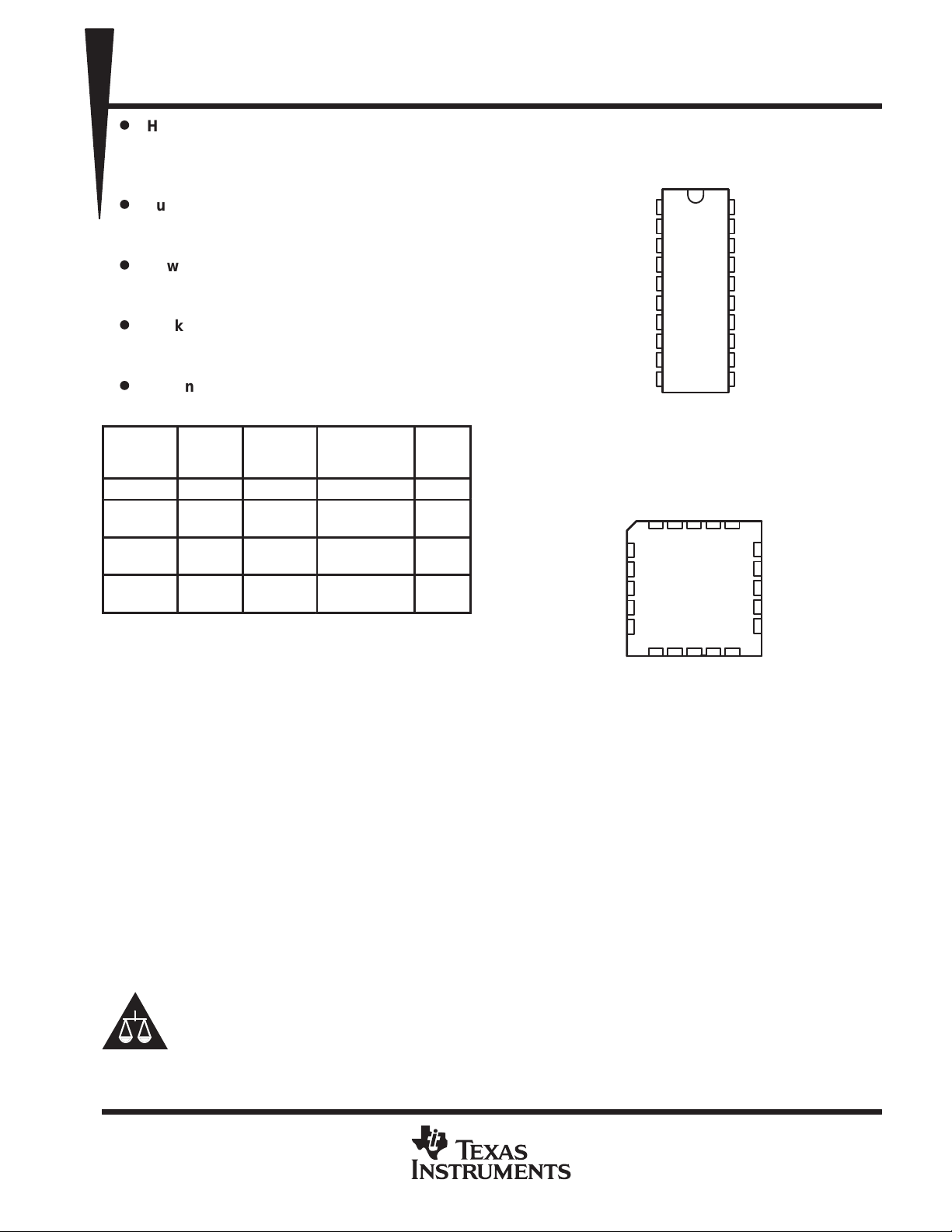
C SUFFIX ...J OR N PACKAGE
M SUFFIX ...J OR W PACKAGE
TIBPAL16L8’
(TOP VIEW)
I
1
I
2
I
3
I
4
5
I
6
I
7
I
8
I
9
I
GND
C SUFFIX . . . FN PACKAGE
M SUFFIX . . . FK PACKAGE
I
I
I
I
I
10
TIBPAL16L8’
(TOP VIEW)
I
I
3212019
4
5
6
7
8
910111213
I
V
20
CC
O
19
I/O
18
I/O
17
16
I/O
15
I/O
14
I/O
13
I/O
12
O
11
I
CC
I
O
V
18
17
16
15
14
I
O
I/O
I/O
I/O
I/O
I/O
I/O
GND
The TIBP AL16’ C series is characterized from 0°C
to 75°C. The TIBP AL16’ M series is characterized
for operation over the full military temperature
range of –55°C to 125°C.
Please be aware that an important notice concerning availability, standard warranty, and use in critical applications of
Texas Instruments semiconductor products and disclaimers thereto appears at the end of this data sheet.
These devices are covered by U.S. Patent 4,410,987.
IMPACT is a trademark of Texas Instruments.
PAL is a registered trademark of Advanced Micro Devices Inc.
PRODUCTION DATA information is current as of publication date.
Products conform to specifications per the terms of Texas Instruments
standard warranty. Production processing does not necessarily include
testing of all parameters.
POST OFFICE BOX 655303 • DALLAS, TEXAS 75265
Copyright 2000, Texas Instruments Incorporated
1
TIBPAL 16R4-15C, TIBPAL 16R6-15C, TIBPAL 16R8-15C
TIBPAL 16R4-20M, TIBPAL 16R6-20M, TIBPAL 16R8-20M
HIGH-PERFORMANCE IMPACT PAL CIRCUITS
SRPS019A – FEBRUARY 1984 – REVISED APRIL 2000
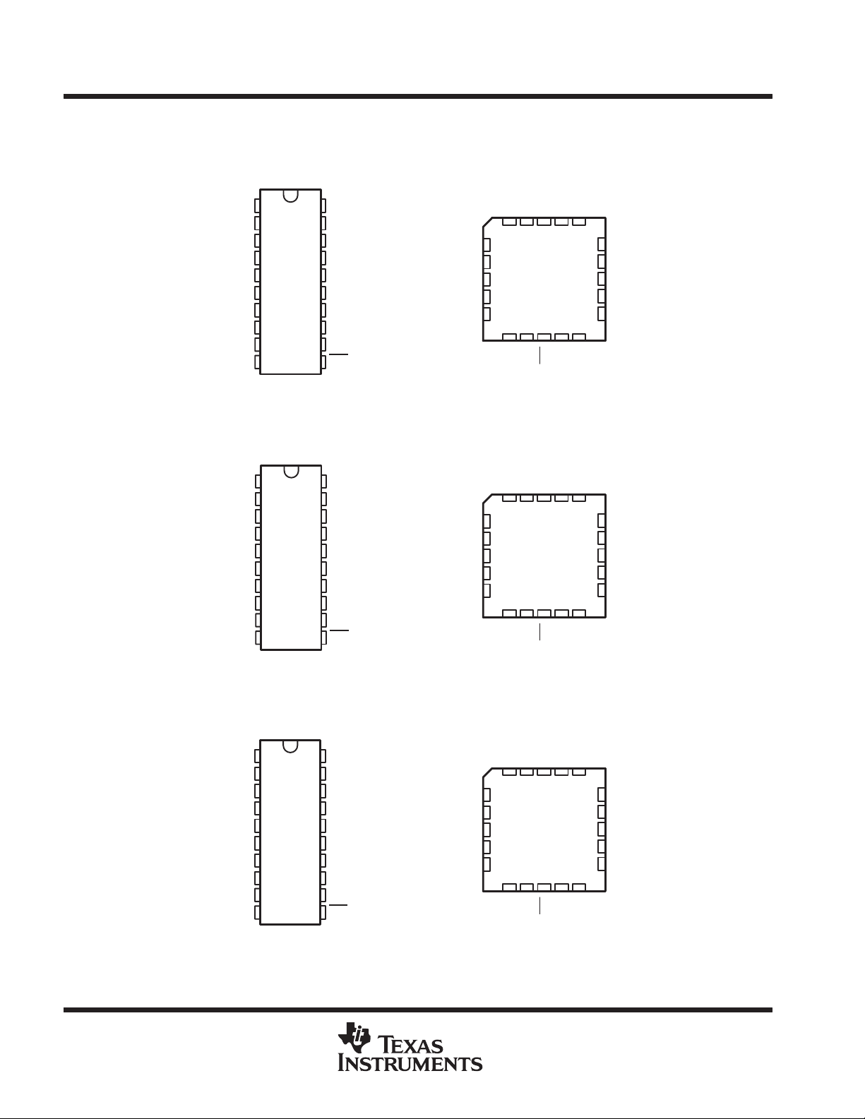
TIBPAL16R4’
C SUFFIX ...J OR N PACKAGE
M SUFFIX ...J OR W PACKAGE
(TOP VIEW)
CLK
1
I
2
I
3
I
4
I
5
I
6
I
7
I
8
I
9
GND
C SUFFIX ...J OR N PACKAGE
M SUFFIX ...J OR W PACKAGE
GND
CLK
I
I
I
I
I
I
I
I
10
TIBPAL16R6’
(TOP VIEW)
1
2
3
4
5
6
7
8
9
10
20
19
18
17
16
15
14
13
12
11
20
19
18
17
16
15
14
13
12
11
V
I/O
I/O
Q
Q
Q
Q
I/O
I/O
OE
V
I/O
Q
Q
Q
Q
Q
Q
I/O
OE
CC
CC
TIBPAL16R4’
C SUFFIX . . . FN PACKAGE
M SUFFIX . . . FK PACKAGE
(TOP VIEW)
I
3212019
I
4
I
5
I
6
I
7
8
I
910111213
CC
I
CLK
I/O
V
18
17
16
15
14
I
I/O
I/O
OE
GND
TIBPAL16R6’
C SUFFIX . . . FN PACKAGE
M SUFFIX . . . FK PACKAGE
(TOP VIEW)
I
GND
CLK
OE
CC
V
I/O
I/O
18
17
16
15
14
Q
I
3212019
I
4
I
5
I
6
I
7
I
8
910111213
I
I/O
Q
Q
Q
Q
Q
Q
Q
Q
Q
TIBPAL16R8’
C SUFFIX ...J OR N PACKAGE
M SUFFIX ...J OR W PACKAGE
(TOP VIEW)
CLK
1
I
2
I
3
I
4
I
5
I
6
I
7
I
8
I
9
GND
2
10
V
20
CC
19
Q
18
Q
17
Q
16
Q
15
Q
14
Q
13
Q
12
Q
11
OE
POST OFFICE BOX 655303 • DALLAS, TEXAS 75265
TIBPAL16R8’
C SUFFIX . . . FN PACKAGE
M SUFFIX . . . FK PACKAGE
(TOP VIEW)
I
GND
CLK
OE
V
Q
CC
Q
18
17
16
15
14
Q
I
3212019
I
4
I
5
I
6
I
7
I
8
910111213
I
Q
Q
Q
Q
Q
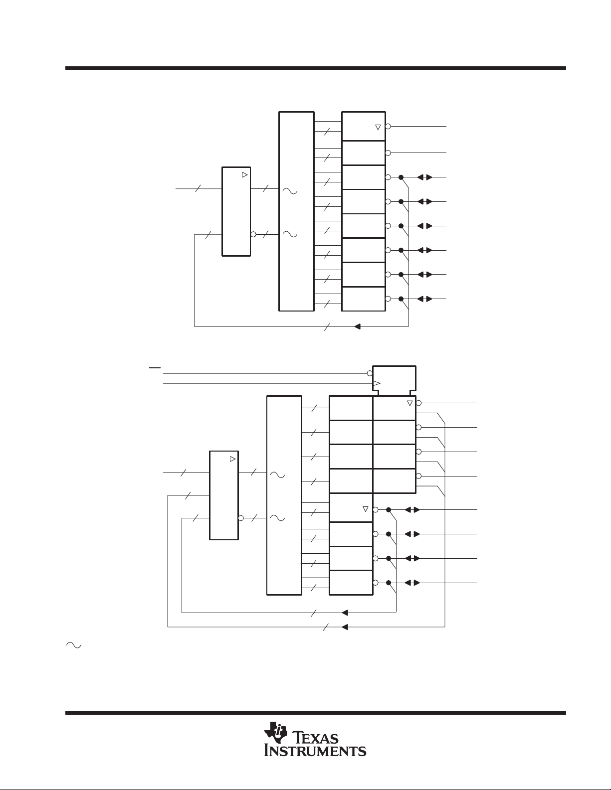
functional block diagrams (positive logic)
TIBPAL 16L8-15C, TIBPAL 16R4-15C
TIBPAL 16L8-20M, TIBPAL 16R4-20M
HIGH-PERFORMANCE IMPACT PAL CIRCUITS
SRPS019A – FEBRUARY 1984 – REVISED APRIL 2000
TIBPAL16L8 ’
OE
CLK
10 16
I
16 ×
166
32 × 64
TIBPAL16R4’
&
32 × 64
&
7
7
7
7
7
7
7
7
6
8
8
EN
≥ 1
≥ 1
EN 2
C1
I = 1
1D
O
O
I/O
I/O
I/O
I/O
I/O
I/O
2
Q
Q
denotes fused inputs
816
I
16 ×
4
164
8
8
≥ 1
EN
7
7
7
7
4
4
Q
Q
I/O
I/O
I/O
I/O
POST OFFICE BOX 655303 • DALLAS, TEXAS 75265
3
TIBPAL 16R6-15C, TIBPAL 16R8-15C
TIBPAL 16R6-20M, TIBPAL 16R8-20M
HIGH-PERFORMANCE IMPACT PAL CIRCUITS
SRPS019A – FEBRUARY 1984 – REVISED APRIL 2000
functional block diagrams (positive logic)
TIBPAL16R6 ’
OE
CLK
OE
CLK
816
I
16 ×
6
162
&
32 × 64
TIBPAL16R8’
EN 2
C1
1D
EN 2
I = 1
C1
2
Q
Q
Q
Q
Q
Q
I/O
I/O
8
8
8
8
8
8
7
7
2
≥ 1
≥ 1
EN
6
denotes fused inputs
816
I
16 ×
168
&
32 × 64
1D
I = 1
2
Q
Q
Q
Q
Q
Q
Q
Q
8
8
8
8
8
8
8
8
8
≥ 1
4
POST OFFICE BOX 655303 • DALLAS, TEXAS 75265
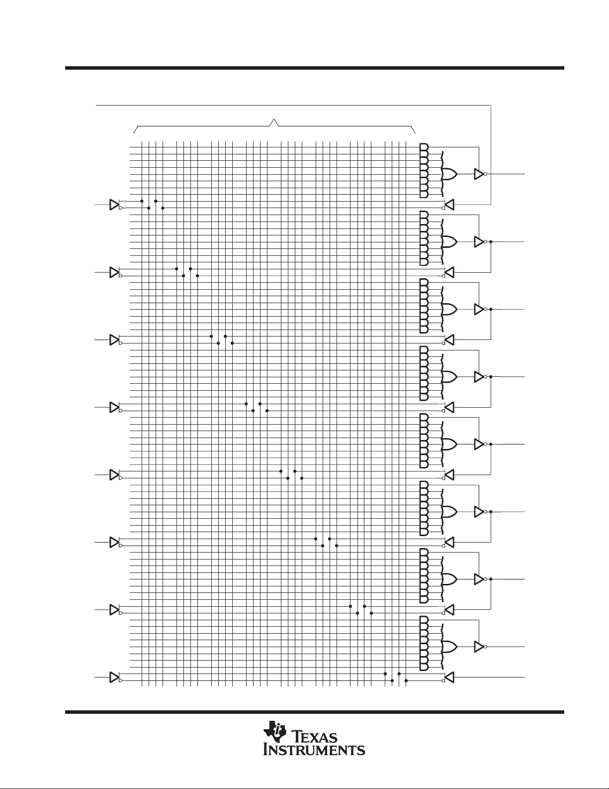
logic diagram (positive logic)
1
I
First
Fuse
Numbers
2
I
3
I
4
I
5
I
6
I
7
I
8
I
9
I
Fuse number = First fuse number + Increment
0 4 8 12 16 20 24 28 31
0
32
64
96
128
160
192
224
256
288
320
352
384
416
448
480
512
544
576
608
640
672
704
736
768
800
832
864
896
928
960
992
1024
1056
1088
1120
1152
1184
1216
1248
1280
1312
1344
1376
1408
1440
1472
1504
1536
1568
1600
1632
1664
1696
1728
1760
1792
1824
1856
1888
1920
1952
1984
2016
Increment
TIBPAL 16L8-15C
TIBPAL 16L8-20M
HIGH-PERFORMANCE IMPACT PAL CIRCUITS
SRPS019A – FEBRUARY 1984 – REVISED APRIL 2000
19
O
18
I/O
17
I/O
16
I/O
15
I/O
14
I/O
13
I/O
12
O
11
I
POST OFFICE BOX 655303 • DALLAS, TEXAS 75265
5
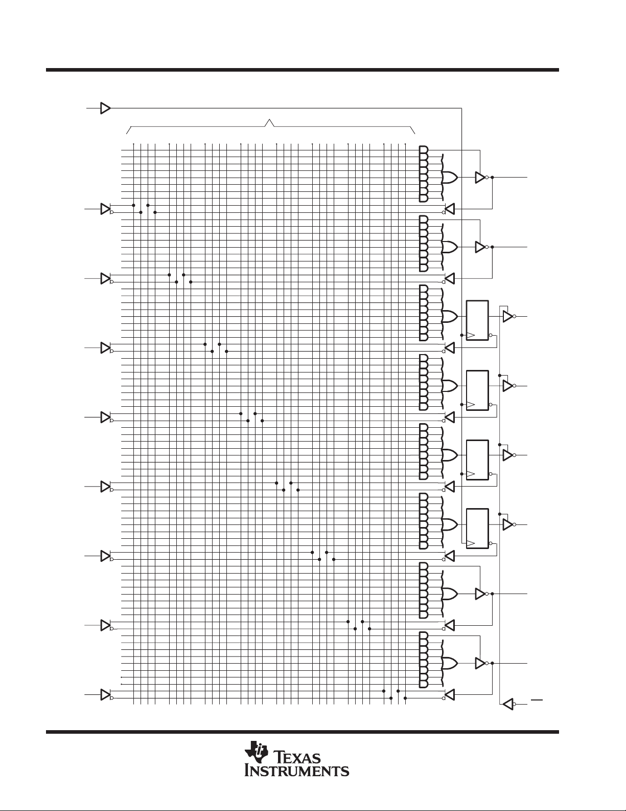
TIBPAL 16R4-15C
TIBPAL 16R4-20M
HIGH-PERFORMANCE IMPACT PAL CIRCUITS
SRPS019A – FEBRUARY 1984 – REVISED APRIL 2000
logic diagram (positive logic)
1
CLK
First
Fuse
Numbers
2
I
3
I
4
I
5
I
6
I
7
I
8
I
9
I
0 4 8 12 16 20 24 28 31
0
32
64
96
128
160
192
224
256
288
320
352
384
416
448
480
512
544
576
608
640
672
704
736
768
800
832
864
896
928
960
992
1024
1056
1088
1120
1152
1184
1216
1248
1280
1312
1344
1376
1408
1440
1472
1504
1536
1568
1600
1632
1664
1696
1728
1760
1792
1824
1856
1888
1920
1952
1984
2016
Fuse number = First fuse number + Increment
Increment
I = 1
1D
I = 1
1D
I = 1
1D
I = 1
1D
C1
C1
C1
C1
19
18
17
16
15
14
13
12
11
I/O
I/O
Q
Q
Q
Q
I/O
I/O
OE
6
POST OFFICE BOX 655303 • DALLAS, TEXAS 75265

logic diagram (positive logic)
1
CLK
First
Fuse
Numbers
2
I
3
I
4
I
5
I
6
I
7
I
8
I
9
I
Fuse number = First fuse number + Increment
0 4 8 12 16 20 24 28 31
0
32
64
96
128
160
192
224
256
288
320
352
384
416
448
480
512
544
576
608
640
672
704
736
768
800
832
864
896
928
960
992
1024
1056
1088
1120
1152
1184
1216
1248
1280
1312
1344
1376
1408
1440
1472
1504
1536
1568
1600
1632
1664
1696
1728
1760
1792
1824
1856
1888
1920
1952
1984
2016
TIBPAL 16R6-15C
TIBPAL 16R6-20M
HIGH-PERFORMANCE IMPACT PAL CIRCUITS
SRPS019A – FEBRUARY 1984 – REVISED APRIL 2000
Increment
I = 1
1D
C1
I = 1
1D
C1
I = 1
1D
C1
I = 1
1D
C1
I = 1
1D
C1
I = 1
1D
C1
19
18
17
16
15
14
13
12
11
I/O
Q
Q
Q
Q
Q
Q
I/O
OE
POST OFFICE BOX 655303 • DALLAS, TEXAS 75265
7

TIBPAL 16R8-15C
TIBPAL 16R8-20M
HIGH-PERFORMANCE IMPACT PAL CIRCUITS
SRPS019A – FEBRUARY 1984 – REVISED APRIL 2000
logic diagram (positive logic)
1
CLK
First
Fuse
Numbers
2
I
3
I
4
I
5
I
6
I
7
I
8
I
9
I
0 4 8 12 16 20 24 28 31
0
32
64
96
128
160
192
224
256
288
320
352
384
416
448
480
512
544
576
608
640
672
704
736
768
800
832
864
896
928
960
992
1024
1056
1088
1120
1152
1184
1216
1248
1280
1312
1344
1376
1408
1440
1472
1504
1536
1568
1600
1632
1664
1696
1728
1760
1792
1824
1856
1888
1920
1952
1984
2016
Fuse number = First fuse number + Increment
Increment
I = 1
1D
I = 1
1D
I = 1
1D
I = 1
1D
I = 1
1D
I = 1
1D
I = 1
1D
I = 1
1D
C1
C1
C1
C1
C1
C1
C1
C1
19
18
17
16
15
14
13
12
11
Q
Q
Q
Q
Q
Q
Q
Q
OE
8
POST OFFICE BOX 655303 • DALLAS, TEXAS 75265

twPulse duration, clock (see Note 2)
ns
TIBPAL 16L8-15C, TIBPAL 16R4-15C, TIBPAL 16R6-15C, TIBPAL 16R8-15C
HIGH-PERFORMANCE IMPACT PAL CIRCUITS
SRPS019A – FEBRUARY 1984 – REVISED APRIL 2000
absolute maximum ratings over operating free-air temperature range (unless otherwise noted)
Supply voltage, VCC (see Note 1) 7 V. . . . . . . . . . . . . . . . . . . . . . . . . . . . . . . . . . . . . . . . . . . . . . . . . . . . . . . . . . . .
Input voltage (see Note 1) 5.5 V. . . . . . . . . . . . . . . . . . . . . . . . . . . . . . . . . . . . . . . . . . . . . . . . . . . . . . . . . . . . . . . . . .
Voltage applied to disabled output (see Note 1) 5.5 V. . . . . . . . . . . . . . . . . . . . . . . . . . . . . . . . . . . . . . . . . . . . . . .
Operating free-air temperature range 0°C to 75°C. . . . . . . . . . . . . . . . . . . . . . . . . . . . . . . . . . . . . . . . . . . . . . . . . .
Storage temperature range, T
NOTE 1: These ratings apply, except for programming pins, during a programming cycle.
recommended operating conditions
V
V
V
I
OH
I
OL
f
clock
t
su
t
h
T
NOTE 2: The total clock period of clock high and clock low must not exceed clock frequency, f
Supply voltage 4.75 5 5.25 V
CC
High-level input voltage 2 5.5 V
IH
Low-level input voltage 0.8 V
IL
High-level output current –3.2 mA
Low-level output current 24 mA
Clock frequency 0 50 MHz
Setup time, input or feedback before clock↑ 15 ns
Hold time, input or feedback after clock↑ 0 ns
Operating free-air temperature 0 25 75 °C
A
clock high or low only, but not for both simultaneously.
–65°C to 150°C. . . . . . . . . . . . . . . . . . . . . . . . . . . . . . . . . . . . . . . . . . . . . . . . . . .
stg
MIN NOM MAX UNIT
High 8
Low 9
. The minimum pulse durations specified are for
clock
POST OFFICE BOX 655303 • DALLAS, TEXAS 75265
9

TIBPAL 16L8-15C, TIBPAL 16R4-15C, TIBPAL 16R6-15C, TIBPAL 16R8-15C
I
V
V
V
A
I
V
V
V
A
,
R1 500 Ω,
HIGH-PERFORMANCE IMPACT PAL CIRCUITS
SRPS019A – FEBRUARY 1984 – REVISED APRIL 2000
electrical characteristics over recommended operating free-air temperature range
PARAMETER TEST CONDITIONS MIN TYP†MAX UNIT
V
IK
V
OH
V
OL
OZH
OZL
I
I
I
IH
I
IL
I
O
I
CC
†
All typical values are at VCC = 5 V, TA = 25°C.
‡
The output conditions have been chosen to produce a current that closely approximates one-half of the short-circuit output current, IOS.
Outputs
I/O ports
Outputs
I/O ports
‡
switching characteristics over recommended ranges of supply voltage and operating free-air
temperature (unless otherwise noted)
PARAMETER
f
max
t
pd
t
pd
t
en
t
dis
t
en
t
dis
†
All typical values are at VCC = 5 V, TA = 25°C.
VCC = 4.75 V, II = –18 mA –1.5 V
VCC = 4.75 V, IOH = –3.2 mA 2.4 3.3 V
VCC = 4.75 V, IOL = 24 mA 0.35 0.5 V
= 5.25 V,
CC
= 5.25 V,
CC
VCC = 5.25 V, VI = 5.5 V 0.1 mA
VCC = 5.25 V, VI = 2.7 V 20 µA
VCC = 5.25 V, VI = 0.4 V –0.2 mA
VCC = 5.25 V, VO = 2.25 V –30 –125 mA
VCC = 5.25 V, VI = 0, Outputs open 140 180 mA
FROM
(INPUT)
I, I/O O, I/O
CLK↑ Q
OE↓ Q
OE↑ Q
I, I/O O, I/O 10 15 ns
I, I/O O, I/O 10 15 ns
= 2.7
O
= 0.4
O
TO
(OUTPUT)
TEST CONDITIONS MIN TYP†MAX UNIT
50 MHz
10 15 ns
R1 = 500 Ω
R2 = 500 Ω,
See Figure 3
8 12 ns
8 12 ns
7 10 ns
20
100
–20
–250
µ
µ
10
POST OFFICE BOX 655303 • DALLAS, TEXAS 75265

twPulse duration, clock (see Note 2)
ns
TIBPAL 16L8-20M, TIBPAL 16R4-20M, TIBPAL 16R6-20M, TIBPAL 16R8-20M
HIGH-PERFORMANCE IMPACT PAL CIRCUITS
SRPS019A – FEBRUARY 1984 – REVISED APRIL 2000
absolute maximum ratings over operating free-air temperature range (unless otherwise noted)
Supply voltage, VCC (see Note 1) 7 V. . . . . . . . . . . . . . . . . . . . . . . . . . . . . . . . . . . . . . . . . . . . . . . . . . . . . . . . . . . .
Input voltage (see Note 1) 5.5 V. . . . . . . . . . . . . . . . . . . . . . . . . . . . . . . . . . . . . . . . . . . . . . . . . . . . . . . . . . . . . . . . . .
Voltage applied to disabled output (see Note 1) 5.5 V. . . . . . . . . . . . . . . . . . . . . . . . . . . . . . . . . . . . . . . . . . . . . . .
Operating free-air temperature range –55°C to 125°C. . . . . . . . . . . . . . . . . . . . . . . . . . . . . . . . . . . . . . . . . . . . . . .
Storage temperature range, T
NOTE 1: These ratings apply, except for programming pins, during a programming cycle.
recommended operating conditions
V
V
V
I
OH
I
OL
f
clock
t
su
t
h
T
NOTE 2: The total clock period of clock high and clock low must not exceed clock frequency, f
Supply voltage 4.5 5 5.5 V
CC
High-level input voltage 2 5.5 V
IH
Low-level input voltage 0.8 V
IL
High-level output current –2 mA
Low-level output current 12 mA
Clock frequency 0 41.6 MHz
Setup time, input or feedback before clock↑ 20 ns
Hold time, input or feedback after clock↑ 0 ns
Operating free-air temperature –55 25 125 °C
A
clock high or low only, but not for both simultaneously.
–65°C to 150°C. . . . . . . . . . . . . . . . . . . . . . . . . . . . . . . . . . . . . . . . . . . . . . . . . . .
stg
MIN NOM MAX UNIT
High 10
Low 11
. The minimum pulse durations specified are for
clock
POST OFFICE BOX 655303 • DALLAS, TEXAS 75265
11

TIBPAL 16L8-20M, TIBPAL 16R4-20M, TIBPAL 16R6-20M, TIBPAL 16R8-20M
I
V
V
V
A
I
V
V
V
A
I
V
V
V
mA
I
V
V
V
mA
,
R1 390 Ω,
HIGH-PERFORMANCE IMPACT PAL CIRCUITS
SRPS019A – FEBRUARY 1984 – REVISED APRIL 2000
electrical characteristics over recommended operating free-air temperature range
PARAMETER TEST CONDITIONS MIN TYP†MAX UNIT
V
IK
V
OH
V
OL
OZH
OZL
I
I
IH
IL
I
OS
I
CC
†
All typical values are at VCC = 5 V, TA = 25°C.
‡
Not more than one output should be shorted at a time and the duration of the short circuit should not exceed one second. Set VO at 0.5 V to avoid
test-equipment degradation.
Outputs
I/O ports
Outputs
I/O ports
Pin 1, 11
All others
Pin 1, 11 50
I/O ports
All others 20
I/O ports
All others
‡
VCC = 4.5 V, II = –18 mA –1.5 V
VCC = 4.5 V, IOH = –2 mA 2.4 3.2 V
VCC = 4.5 V, IOL = 12 mA 0.25 0.4 V
= 5.5 V,
CC
= 5.5 V,
CC
= 5.5 V,
CC
VCC = 5.5 V, VI = 2.7 V
= 5.5 V,
CC
VCC = 5.5 V, VO = 0.5 V –30 –250 mA
VCC = 5.5 V, VI = 0, Outputs open 140 190 mA
= 2.7
O
= 0.4
O
= 5.5
I
= 0.4
I
20
100
–20
–250
0.2
0.1
100
–0.25
–0.2
µ
µ
µA
switching characteristics over recommended ranges of supply voltage and operating free-air
temperature (unless otherwise noted)
PARAMETER
f
max
t
pd
t
pd
t
en
t
dis
t
en
t
dis
†
All typical values are at VCC = 5 V, TA = 25°C.
FROM
(INPUT)
I, I/O O, I/O
CLK↑ Q
OE↓ Q
OE↑ Q
I, I/O O, I/O 10 20 ns
I, I/O O, I/O 10 20 ns
TO
(OUTPUT)
TEST CONDITIONS MIN TYP†MAX UNIT
41.6 MHz
10 20 ns
R1 = 390 Ω
R2 = 750 Ω,
See Figure 4
8 15 ns
8 15 ns
7 15 ns
12
POST OFFICE BOX 655303 • DALLAS, TEXAS 75265

TIBPAL 16L8-15C, TIBPAL 16R4-15C, TIBPAL 16R6-15C, TIBPAL 16R8-15C
TIBPAL 16L8-20M, TIBPAL 16R4-20M, TIBPAL 16R6-20M, TIBPAL 16R8-20M
HIGH-PERFORMANCE IMPACT PAL CIRCUITS
SRPS019A – FEBRUARY 1984 – REVISED APRIL 2000
programming information
Texas Instruments programmable logic devices can be programmed using widely available software and
inexpensive device programmers.
Complete programming specifications, algorithms, and the latest information on hardware, software, and
firmware are available upon request. Information on programmers capable of programming T exas Instruments
programmable logic also is available, upon request, from the nearest TI field sales office or local authorized TI
distributor, by calling Texas Instruments at +1 (972) 644–5580, or by visiting the TI Semiconductor Home Page
at www.ti.com/sc.
preload procedure for registered outputs (see Figure 1 and Note 3)
The output registers can be preloaded to any desired state during device testing. This permits any state to be
tested without having to step through the entire state-machine sequence. Each register is preloaded individually
by following the steps given below.
Step 1. With V
Step 2. Apply either V
at 5 V and Pin 1 at VIL, raise Pin 11 to V
CC
or VIH to the output corresponding to the register to be preloaded.
IL
IHH
.
Step 3. Pulse Pin 1, clocking in preload data.
Step 4. Remove output voltage, then lower Pin 11 to VIL. Preload can be verified by observing the
voltage level at the output pin.
V
V
V
V
V
V
IHH
IL
IH
IL
OH
OL
Pin 11
t
d
Pin 1
Registered I/O
NOTE 3: td = tsu = th = 100 ns to 1000 ns V
t
su
= 10.25 V to 10.75 V
IHH
t
t
w
Input Output
d
V
IH
V
IL
Figure 1. Preload Waveforms
POST OFFICE BOX 655303 • DALLAS, TEXAS 75265
13

TIBPAL 16L8-15C, TIBPAL 16R4-15C, TIBPAL 16R6-15C, TIBPAL 16R8-15C
TIBPAL 16L8-20M, TIBPAL 16R4-20M, TIBPAL 16R6-20M, TIBPAL 16R8-20M
HIGH-PERFORMANCE IMPACT PAL CIRCUITS
SRPS019A – FEBRUARY 1984 – REVISED APRIL 2000
power-up reset (see Figure 2)
Following power up, all registers are set high. This feature provides extra flexibility to the system designer and
is especially valuable in simplifying state-machine initialization. T o ensure a valid power-up reset, it is important
that the rise of VCC be monotonic. Following power-up reset, a low-to-high clock transition must not occur until
all applicable input and feedback setup times are met.
V
CC
Active-Low
Registered Output
CLK
†
This is the power-up reset time and applies to registered outputs only. The values shown are from characterization data.
‡
This is the setup time for input or feedback.
4 V
†
t
pd
(600 ns TYP, 1000 ns MAX)
1.5 V
1.5 V
t
t
w
su
‡
1.5 V
Figure 2. Power-Up Reset Waveforms
5 V
V
V
V
V
OH
OL
IH
IL
14
POST OFFICE BOX 655303 • DALLAS, TEXAS 75265

TIBPAL 16L8-15C, TIBPAL 16R4-15C, TIBPAL 16R6-15C, TIBPAL 16R8-15C
HIGH-PERFORMANCE IMPACT PAL CIRCUITS
SRPS019A – FEBRUARY 1984 – REVISED APRIL 2000
PARAMETER MEASUREMENT INFORMATION
7 V
S1
R1
From Output
Under Test
C
(see Note A)
LOAD CIRCUIT FOR 3-STATE OUTPUTS
L
Test
Point
R2
Timing
Input
t
su
Data
Input
VOLTAGE WAVEFORMS
SETUP AND HOLD TIMES
Input
t
pd
In-Phase
Output
t
pd
Out-of-Phase
Output
(see Note D)
VOLTAGE WAVEFORMS
PROPAGATION DELAY TIMES
NOTES: A. CL includes probe and jig capacitance and is 50 pF for tpd and ten, 5 pF for t
B. Waveform 1 is for an output with internal conditions such that the output is low except when disabled by the output control. Waveform
2 is for an output with internal conditions such that the output is high except when disabled by the output control.
C. All input pulses have the following characteristics: PRR ≤ 1 MHz, tr = tf ≤ 2 ns, duty cycle = 50%
D. When measuring propagation delay times of 3-state outputs from low to high, switch S1 is closed.
When measuring propagation delay times of 3-state outputs from high to low, switch S1 is open.
E. Equivalent loads may be used for testing.
1.3 V
1.3 V 1.3 V
1.3 V 1.3 V
1.3 V 1.3 V
1.3 V 1.3 V
3.5 V
0.3 V
t
h
3.5 V
0.3 V
3.5 V
0.3 V
t
pd
V
OH
V
OL
t
pd
V
OH
V
OL
High-Level
Pulse
Low-Level
Pulse
Output
Control
(low-level
enabling)
t
en
Waveform 1
S1 Closed
(see Note B)
t
en
Waveform 2
S1 Open
(see Note B)
ENABLE AND DISABLE TIMES, 3-STATE OUTPUTS
1.3 V 1.3 V
t
w
1.3 V
VOLTAGE WAVEFORMS
PULSE DURATIONS
1.3 V 1.3 V
t
dis
1.3 V
t
dis
1.3 V
VOLTAGE WAVEFORMS
.
dis
1.3 V
3.5 V
0.3 V
3.5 V
0.3 V
3.5 V
0.3 V
≈3.5 V
VOL + 0.3 V
V
OL
V
OH
VOH – 0.3 V
≈0 V
Figure 3. Load Circuit and Voltage Waveforms
POST OFFICE BOX 655303 • DALLAS, TEXAS 75265
15

TIBPAL 16L8-20M, TIBPAL 16R4-20M, TIBPAL 16R6-20M, TIBPAL 16R8-20M
HIGH-PERFORMANCE IMPACT PAL CIRCUITS
SRPS019A – FEBRUARY 1984 – REVISED APRIL 2000
PARAMETER MEASUREMENT INFORMATION
5 V
S1
R1
From Output
Under Test
C
(see Note A)
LOAD CIRCUIT FOR 3-STATE OUTPUTS
L
Test
Point
R2
Timing
Input
t
su
Data
Input
VOLTAGE WAVEFORMS
SETUP AND HOLD TIMES
Input
t
pd
In-Phase
Output
t
pd
Out-of-Phase
Output
(see Note D)
VOLTAGE WAVEFORMS
PROPAGATION DELAY TIMES
NOTES: A. CL includes probe and jig capacitance and is 50 pF for tpd and ten, 5 pF for t
B. Waveform 1 is for an output with internal conditions such that the output is low except when disabled by the output control. Waveform
2 is for an output with internal conditions such that the output is high except when disabled by the output control.
C. All input pulses have the following characteristics: PRR ≤ 10 MHz, tr = tf ≤ 2 ns, duty cycle = 50%
D. When measuring propagation delay times of 3-state outputs, switch S1 is closed.
E. Equivalent loads may be used for testing.
1.5 V
1.5 V 1.5 V
1.5 V 1.5 V
1.5 V
1.5 V
3 V
0
t
h
3 V
0
3 V
0
t
pd
V
OH
1.5 V
V
OL
t
pd
V
OH
1.5 V
V
OL
High-Level
Pulse
Low-Level
Pulse
Output
Control
(low-level
enabling)
t
en
Waveform 1
S1 Closed
(see Note B)
t
en
Waveform 2
S1 Open
(see Note B)
ENABLE AND DISABLE TIMES, 3-STATE OUTPUTS
1.5 V 1.5 V
t
w
1.5 V 1.5 V
VOLTAGE WAVEFORMS
PULSE DURATIONS
1.5 V 1.5 V
t
dis
1.5 V
t
dis
1.5 V
VOLTAGE WAVEFORMS
.
dis
3 V
0
3 V
0
3 V
0
≈3.3 V
VOL + 0.5 V
V
OL
V
OH
VOH – 0.5 V
≈0 V
16
Figure 4. Load Circuit and Voltage Waveforms
POST OFFICE BOX 655303 • DALLAS, TEXAS 75265

IMPORTANT NOTICE
T exas Instruments and its subsidiaries (TI) reserve the right to make changes to their products or to discontinue
any product or service without notice, and advise customers to obtain the latest version of relevant information
to verify, before placing orders, that information being relied on is current and complete. All products are sold
subject to the terms and conditions of sale supplied at the time of order acknowledgment, including those
pertaining to warranty, patent infringement, and limitation of liability.
TI warrants performance of its semiconductor products to the specifications applicable at the time of sale in
accordance with TI’s standard warranty. Testing and other quality control techniques are utilized to the extent
TI deems necessary to support this warranty . Specific testing of all parameters of each device is not necessarily
performed, except those mandated by government requirements.
Customers are responsible for their applications using TI components.
In order to minimize risks associated with the customer’s applications, adequate design and operating
safeguards must be provided by the customer to minimize inherent or procedural hazards.
TI assumes no liability for applications assistance or customer product design. TI does not warrant or represent
that any license, either express or implied, is granted under any patent right, copyright, mask work right, or other
intellectual property right of TI covering or relating to any combination, machine, or process in which such
semiconductor products or services might be or are used. TI’s publication of information regarding any third
party’s products or services does not constitute TI’s approval, warranty or endorsement thereof.
Copyright 2000, Texas Instruments Incorporated
 Loading...