

TCM4400E
GSM/DCS BASEBAND AND VOICE A/D
AND D/A RF INTERFACE CIRCUIT
SLWS082A – JULY 1999 – REVISED MARCH 2000
1
POST OFFICE BOX 655303 • DALLAS, TEXAS 75265
D
Applications Include GSM 900,
PCS 1900, and DCS 1800 Cellular
Telephones
D
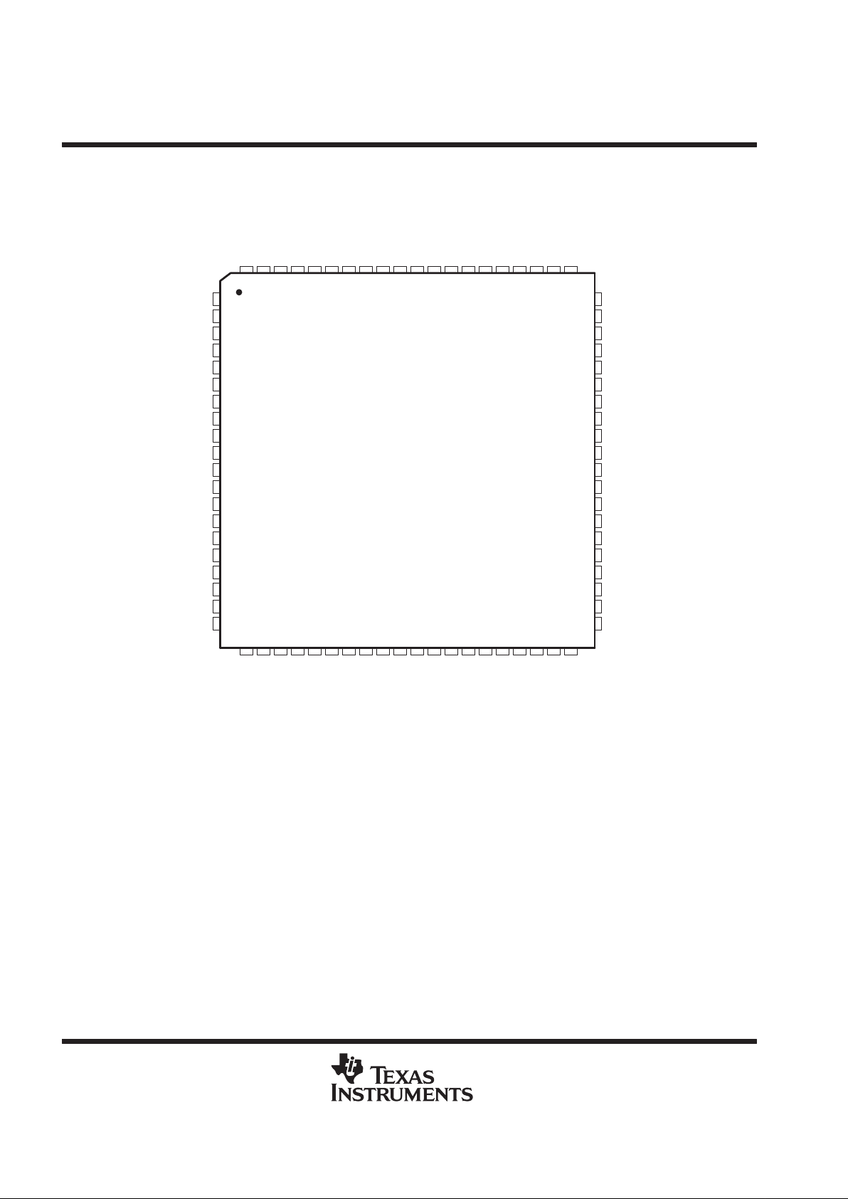
80-Pin TQFP (0.4 mm or 0.5 mm Lead
Pitch) or 80-Ball MicroStar BGA
Packages
D
Single 3-V Supply Voltage
D
Internal Voltage Reference
D
Extended RF Control Voltages
D
Advanced Power Management
D
GSM-Digital Audio Interface (DAI)
D
MCU and DSP Serial Interface
D
Five Ports Auxiliary A/D
D
Meets JTAG Testability Standard (IEEE
Std 1131.1-1990)
D
Baseband Codec-GMSK Modulator
With On-Chip Burst Buffer
D
Voice Codec Features: Microphone
Amplifier and Bias Source,
Programmable Gain Amplifiers, Volume
Control, and Side-Tone Control
description
The TCM4400E global system for mobile communication (GSM) baseband RF interface circuit is designed for
GSM 900 , PCS1900, and DCS 1800 European digital cellular telecommunication systems. It performs the
interface and processing of voice signals, generates baseband in-phase (I) and quadrature (Q) signals, and
controls the signals between a digital signal processor (DSP) and associated RF circuits.
The TCM4400E includes a second serial interface for use with a microcontroller. Through this interface, a
microcontroller can access all the internal registers that can be accessed through the DSP digital serial
interface. This option is intended for applications in which part of the L1 software is implemented in the
microcontroller.
A four-pin parallel port is dedicated to the full control of the digital audio interface (DAI) to the GSM system
simulator; the DAI consists of system simulator reset (SSRST) control, clock generation, and rate adaptation
with the DSP.
The voice processing portion of the device includes microphone and earphone amplifiers, analog-to-digital
(A/D) and digital-to-analog (D/A) converters, speech digital filtering, and a serial port.
The baseband processing portion of the device includes a two-channel uplink path, a two-channel downlink
path, a serial port, and a parallel port. The uplink path performs Gaussian minimum shift keying (GMSK)
modulation and D/A conversion, and it has smoothing filters to provide the external RF circuit with I and Q
baseband signals. The downlink path performs antialiasing, A/D conversion, and channel separation filtering
of the baseband I and Q signals. The serial port allows baseband data exchange with the DSP , and the parallel
port controls precise timing signals.
Auxiliary RF functions such as automatic frequency control (AFC), automatic gain control (AGC), power control,
and analog monitoring are also implemented in the TCM4400E. Internal functional blocks of the device can be
separately and automatically powered down with GSM RF windows.
These devices have limited built-in ESD protection. The leads should be shorted together or the device placed in conductive foam
during storage or handling to prevent electrostatic damage to the MOS gates.
Please be aware that an important notice concerning availability, standard warranty, and use in critical applications of
Texas Instruments semiconductor products and disclaimers thereto appears at the end of this data sheet.
Copyright 2000, Texas Instruments Incorporated
PRODUCTION DATA information is current as of publication date.
Products conform to specifications per the terms of Texas Instruments
standard warranty. Production processing does not necessarily include
testing of all parameters.
MicroStar BGA is a trademark of Texas Instruments.
TCM4400E
GSM/DCS BASEBAND AND VOICE A/D
AND D/A RF INTERFACE CIRCUIT
SLWS082A – JULY 1999 – REVISED MARCH 2000
2
POST OFFICE BOX 655303 • DALLAS, TEXAS 75265
22 23
BULIP
BULIN
BULQP
BULQN
AV
DD2
AV
SS2
BDLIN
BDLIP
BDLQN
BDLQP
VMID
DV
SS3
AV
SS3
APC
AFC
AGC
ADCMID
AV
DD5
DV
DD3
AV
DD3
60
59
58
57
56
55
54
53
52
51
50
49
48
47
46
45
44
43
42
41
24
1
2
3
4
5
6
7
8
9
10
11
12
13
14
15
16
17
18
19
20
BFSX
BCLKX
BDX
BDR
BCLKR
BFSR
AV
DD1
V
REF
IBIAS
VGAP
AV
SS1
RESET
VFS
VDX
VDR
VCLK
SSRST
SSDX
SSDR
SSCLK
25 26 27 28
80-Pin TQFP PACKAGE
(TOP VIEW)
MCLK
79 78 77 76 7580 74
UCLK
UDR
UDX
USEL
BDLON
BULON
BCAL
PWRDN
TRST
GNDA1
MICBIAS
MICIP
MICIN
72 71 7073
29
30 31 32 33
69 68
21
TEST2
67 66 65 64
34 35 36 37
AUXO
GNDA2
TEST3
TCK
ADIN4
38 39 40
TDI
TDO
63 62 61
TEST1
TMS
EARP
ADIN5
DV
DD4
DV
SS4
AV
SS4
DV
DD1DVSS1
BENA
DV
DD2
DV
SS2
AUXI
AV
DD4
EARN
ADIN1
ADIN2
ADIN3
TCM4400E
GSM/DCS BASEBAND AND VOICE A/D
AND D/A RF INTERFACE CIRCUIT
SLWS082A – JULY 1999 – REVISED MARCH 2000
3
POST OFFICE BOX 655303 • DALLAS, TEXAS 75265
109876532 41
J
H
G
F
K
E
D
A
B
C
ADCMID
ADIN1
ADIN2
ADIN3
ADIN4
ADIN5
AFC
AGC
APC
AUXI
AUXO
AV
DD1
AV
DD2
AV
DD3
AV
DD4
AV
DD5
AV
SS1
AV
SS2
AV
SS3
AV
SS4
BCAL
BDR
BDX
BENA
BDLON
BFSR
BFSX
BDLIN
BDLIP
BDLQN
BDLQP
BULIN
BULIP
BULON
BULQN
DV
DD1
DV
DD2
DV
DD3
DV
DD4
DV
SS1
DV
SS2
DV
SS3
DV
SS4
EARN
EARP
GNDA1
GNDA2
IBIAS
TEST1
MICBIAS
MICIP
MICIN
PWRDN
RESET
SSCLK
SSDR
SSDX
SSRST
TCK
TDI
TDO
TEST3
TEST2
MCLK
TMS
TRST
UCLK
UDR
UDX
VCLK
VDR
VDX
VFS
VGAP
VMID
V
REF
NC
NCNC
BCLKX
NC
BULQP
USEL
BCLKR
NC – No internal connection
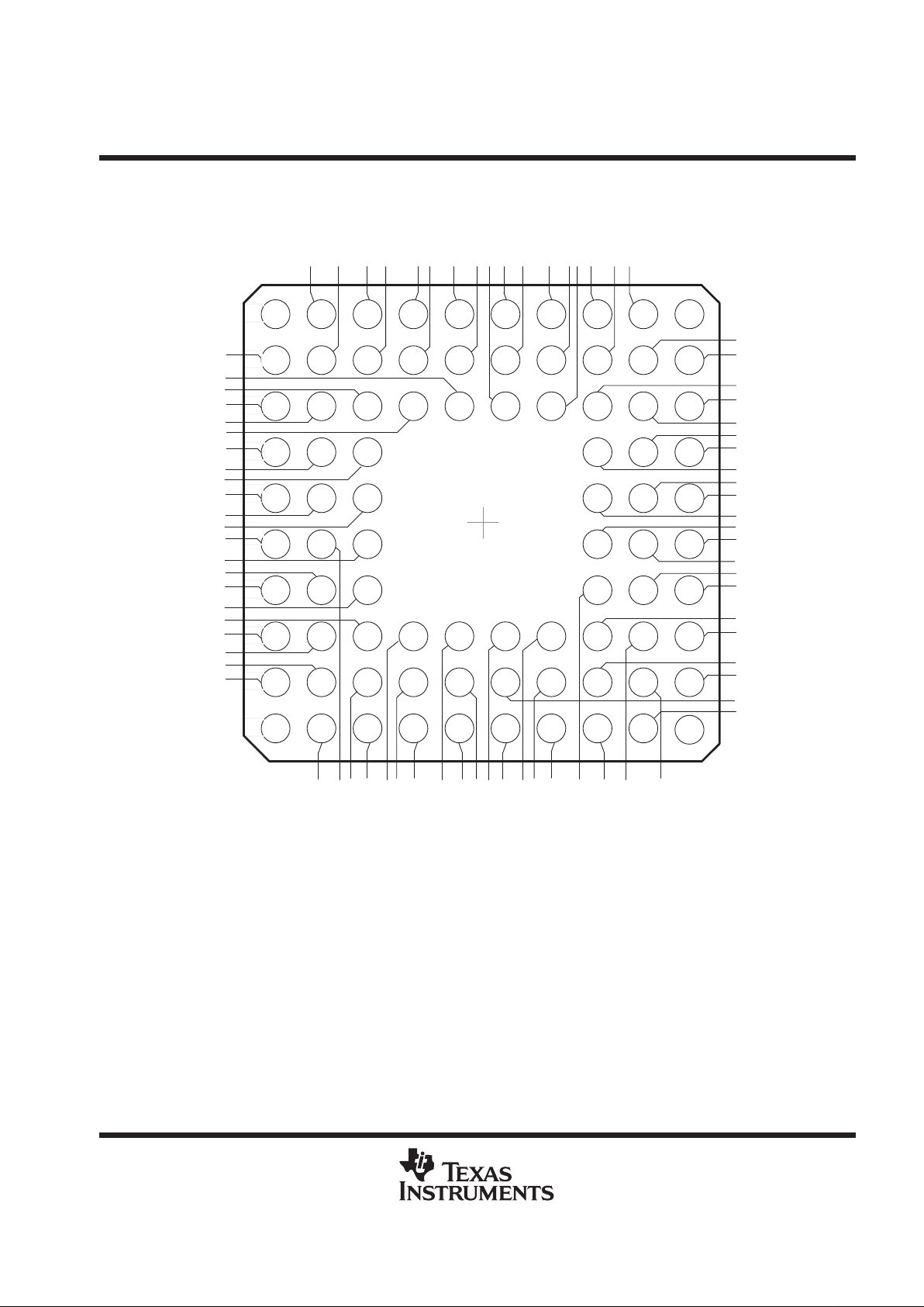
GGM PACKAGE
(TOP VIEW)
B1 B2
A2 A3
D1 D2 D3 D8 D9 D10
K2 K3 K4 K5 K6 K7 K8 K9
J1
F1
E1
C1
H2
G2F2G3
F3
C2 C3
B3
C4 C5 C6 C7 C8 C9
C10
B10
A4 A5 A6 A7 A8 A9
E8 E9 E10
J10
H10
G8 G9 G10
F8 F9 F10
H1
G1
J2 J3 J4 J5 J6 J7 J8 J9
H3 H4 H5 H6 H7 H8 H9
E2 E3
B4 B5 B6 B7 B8 B9
TCM4400E
GSM/DCS BASEBAND AND VOICE A/D
AND D/A RF INTERFACE CIRCUIT
SLWS082A – JULY 1999 – REVISED MARCH 2000
4
POST OFFICE BOX 655303 • DALLAS, TEXAS 75265
functional block diagram
USEL
Main Clock
Generator
GSM Windows
Timing
Interface
JTAG
Interface
Power
Management
Bus
Controller
Auxiliary DAC
Analog AGC
APC (D/A)
RF TX Ramp
MCU
Serial
Interface
DSP
Serial
Interface
Voiceband
Serial
Interface
DAI
Interface
Voice Uplink 13 Bit ADC
Two Analog Inputs
Programmable Gain
Bandpass Digital Filter
Side-tone
Baseband Uplink GMSK Modulator
Internal Burst RAM
Automatic Offset Compensation
8-Bit DAC and Smoothing Filter
Baseband Downlink I/Q Path
Automatic Offset Compensation
10-Bit ADC and Antialiasing Filter
AGC, AFC
APC Output
Swing Control
Voice Downlink 13 Bit DAC
Auxiliary Earphone Output
Programmable Volume
Smoothing Filter
Bandpass Digital Filter
I
REF-VREF
VMID
Bias
AFC (D/A)
VTCXO Control
Auxiliary
10 Bits
5 Inputs ADC
MICBIAS
MICIN
AUXI
MICIP
EARP
EARN
AUXO
MCLK
AGC
TRST
TDO
TDI
TCK
BENA
BCAL
BDLON
BULON
PWRDN
APC
BULIP
BULIN
BULQN
BULQP
BDLIP
BDLIN
BDLQN
BDLQP
AV
DD5
AFC
ADIN1
ADIN2
ADIN3
ADIN4
ADIN5
IBIAS
VREF
VMID
VGAP
UCLK
UDX
UDR
BFSX
BDX
BCLKX
BFSR
BDR
BCLKR
VCLK
VFS
VDX
VDR
SSCLK
SSRST
SSDX
SSDR
TMS
75
78
76
77
1
3
2
6
4
5
16
13
14
15
20
17
18
19
TEST1
TEST2
TEST3
RESET
70
246263
64
71
72
74
73
23
61
696867
12
45
47
60
59
57
58
53
54
52
51
43
46
36
37
38
39
40
26
28
29
27
32
33
34
9
8
50
10
ADCMID
44

TCM4400E
GSM/DCS BASEBAND AND VOICE A/D
AND D/A RF INTERFACE CIRCUIT
SLWS082A – JULY 1999 – REVISED MARCH 2000
5
POST OFFICE BOX 655303 • DALLAS, TEXAS 75265
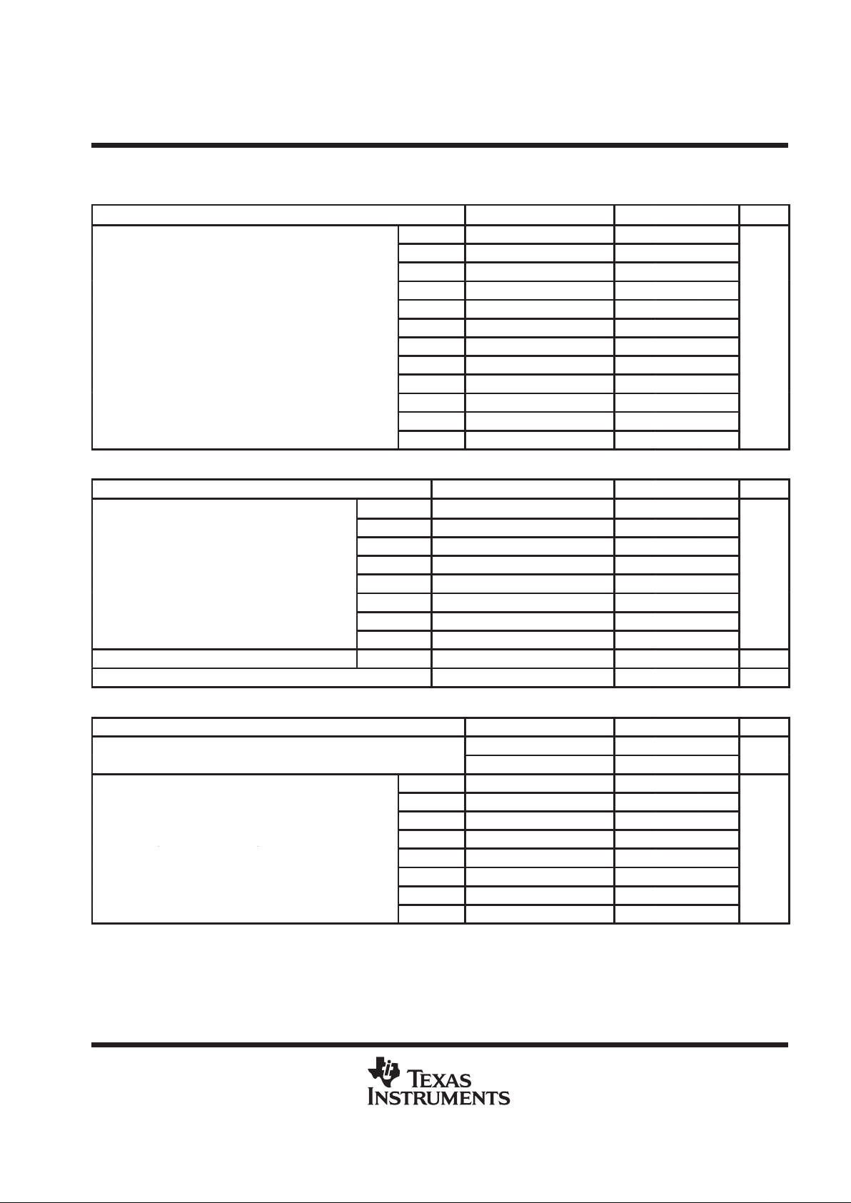
Terminal Functions
TERMINAL
NO.
I/O DESCRIPTION
NAME
QFP BGA
ADCMID 44 H8 I/O Reference voltage of auxiliary A/D converters; decoupling only (analog)
ADIN1 36 J7 I Auxiliary 10-bit ADC input 1 (analog)
ADIN2 37 H7 I Auxiliary 10-bit ADC input 2 (analog)
ADIN3 38 K8 I Auxiliary 10-bit ADC input 5 (analog)
ADIN4 39 J8 I Auxiliary 10-bit ADC input 4 (analog)
ADIN5 40 K9 I Auxiliary 10-bit ADC input 3 (analog)
AFC 46 G9 O Automatic frequency control DAC output (analog)
AGC 45 H10 O Automatic gain control DAC output (analog)
APC 47 G10 O Automatic power control DAC output (analog)
AUXI 29 K5 I Auxiliary (high-level) speech signal input (analog)
AUXO 34 H6 O Auxiliary downlink (voice codec) amplifier output, single-ended (analog)
AV
DD1
7 D1 Analog positive power supply (bandgap, internal common-mode generator, bias current generator).
AV
DD2
56 D9 Analog positive power supply (baseband CODEC)
AV
DD3
41 J9 Analog positive power supply (auxiliary RF functions)
AV
DD4
30 J5 Analog positive power supply (voice codec)
AV
DD5
43 H9 Analog positive power supply (output stages of auxiliary RF functions).
AV
SS1
11 E3 Analog negative power supply (bandgap, internal common-mode generator, bias current generator).
AV
SS2
55 D10 Analog negative power supply (baseband CODEC)
AV
SS3
48 G8 Analog negative power supply (auxiliary RF functions)
AV
SS4
31 H5 Analog negative power supply (voice codec)
BCAL 72 A5 I Baseband uplink or downlink offset calibration enable (timing interface)
BCLKR 5 C1 I/O DSP serial interface clock input. This clock signal is provided by the DSP or the TCM4400E (digital/3-state).
BCLKX 2 B1 O DSP serial interface clock output. The frequency is the same as MCLK (digital/3-state).
BDR 4 C3 I DSP serial interface serial data input (digital)
BDX 3 C2 O DSP serial interface serial data output (digital/3-state)
BENA 71 C6 I Burst transmit or receive enable (depends on status of BULON and BDLON) (digital)
BDLON 74 C5 I Power on of baseband downlink (timing interface)
BFSR 6 D2 I DSP serial interface receive frame synchronization input (digital)
BFSX 1 B2 O DSP serial interface transmit frame synchronization output (digital/3-state)
BDLIN 54 E8 I In-phase baseband input (–) downlink path (analog)
BDLIP 53 E9 I In-phase baseband input (+) downlink path (analog)
BDLQN 52 E10 I Quadrature baseband input (–) downlink path (analog)
BDLQP 51 F8 I Quadrature baseband input (+) downlink path (analog)
BULIN 59 C9 O In-phase baseband output (–) uplink path (analog)
BULIP 60 B10 O In-phase baseband output (+) uplink path (analog)
BULON 73 B5 I Serial clock input (serial interface) (digital)
BULQN 57 D8 O Negative quadrature baseband output. BULQN is an uplink path (analog)
BULQP 58 C10 O Positive quadrature baseband output. BULQN is an uplink path (analog)
DV
DD1
80 A2 Digital positive power supply (baseband and timing serial interfaces)
DV
DD2
66 B7 Digital positive power supply (baseband CODEC)
DV
DD3
42 J10 Digital positive power supply (auxiliary RF functions)

TCM4400E
GSM/DCS BASEBAND AND VOICE A/D
AND D/A RF INTERFACE CIRCUIT
SLWS082A – JULY 1999 – REVISED MARCH 2000
6
POST OFFICE BOX 655303 • DALLAS, TEXAS 75265
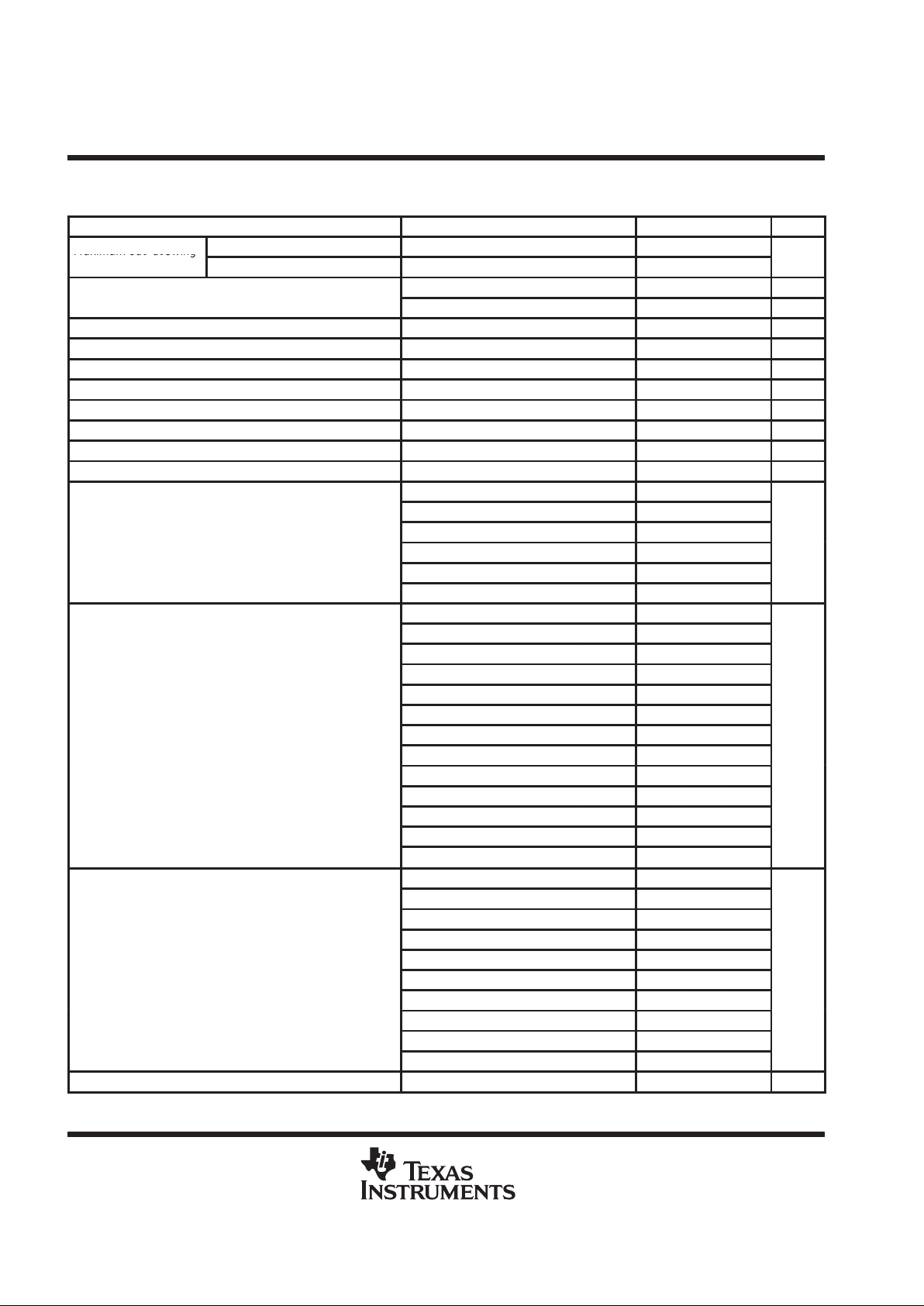
Terminal Functions (Continued)
TERMINAL
NO.
I/O DESCRIPTION
NAME
QFP BGA
DV
DD4
21 J2 Digital positive power supply (voiceband codec and serial interface)
DV
SS1
79 B3 Digital negative power supply (baseband and timing serial interfaces)
DV
SS2
65 A8 Digital negative power supply (baseband CODEC)
DV
SS3
49 F10 Digital negative power supply (auxiliary RF functions)
DV
SS4
22 K2 Digital negative power supply (voiceband codec and serial interface)
EARN 33 J6 O Earphone amplifier output (–) (analog)
EARP 32 K6 O Earphone amplifier output (+) (analog)
GNDA1 25 K3 Analog signal ground for the microphone amplifier and auxiliary input
GNDA2 35 K7 Signal return (ground) for AUXO output
IBIAS 9 E1 I/O Internal bias reference current adjust. IBIAS adjusts the reference current with an external resistor (analog).
MCLK 70 B6 I Master system clock input (13 MHz)
MICBIAS 26 J4 I Microphone bias supply output. MICBIAS is also used to decouple bias supply with an external capacitor
(analog).
MICIP 27 K4 I Positive microphone amplifier input (analog)
MICIN 28 H4 I Negative microphone amplifier input (analog)
PWRDN 23 J3 I Power-down mode control input (digital), active high
RESET 12 F1 I Device global hardware reset (digital), active low
SSCLK 20 J1 O DAI external 104 kHz clock output (digital)
SSDR 19 H2 I DAI data transfer input. SSDR connects to GSM-SS TDAI (digital/pullup).
SSDX 18 H1 O DAI data transfer output SSDX connects to GSM-SS RDAI (digital).
SSRST 17 G3 I DAI reset input (digital/pullup)
TCK 64 C8 I Scan test clock (digital/pulldown)
TDI 63 B8 I Scan path input (for testing purposes) (digital/pullup)
TDO 62 A9 I Scan path output (for testing purposes) (digital/3-state)
TEST1 69 A6 I/O Test I/O (digital/3-state & pullup)
TEST2 68 C7 I/O Test I/O (digital/3-state & pullup)
TEST3 67 A7 O T est output (digital)
TMS 61 B9 I JTAG test mode select (digital/pullup)
TRST 24 H3 I JTAG serial interface & boundary scan register reset (digital/pullup), active low.
UCLK 78 A3 I MCU interface clock input (digital)
UDR 77 C4 I MCU interface data transfer input (digital)
UDX 76 B4 O MCU interface data transfer output (digital/3-state)
USEL 75 A4 I MCU serial interface select (digital)
VCLK 16 G2 O Voiceband serial interface clock output (digital/3-state)
VDR 15 G1 I Voiceband serial interface receive data input (digital)
VDX 14 F3 O Voiceband serial interface transmit data output (digital/3-state)
VFS 13 F2 O Voiceband serial interface transmit frame synchronization output (digital/3-state)
VGAP 10 E2 I/O Bandgap reference voltage. VGAP decouples with an external capacitor (analog)
VMID 50 F9 O Baseband uplink midrail voltage output. VMID serves as a reference common-mode voltage for a RF device
when directly dc coupled (analog)
V
REF
8 D3 I/O Reference voltage V
REF
decouples with an external capacitor (analog).
TCM4400E
GSM/DCS BASEBAND AND VOICE A/D
AND D/A RF INTERFACE CIRCUIT
SLWS082A – JULY 1999 – REVISED MARCH 2000
7
POST OFFICE BOX 655303 • DALLAS, TEXAS 75265
absolute maximum ratings over operating free-air temperature range (unless otherwise noted)
†
Supply voltage range, AVDD, DV
DD
(see Note 1) –0.3 to 6 V. . . . . . . . . . . . . . . . . . . . . . . . . . . . . . . . . . . . . . . . .
Maximum voltage on any input, V
I
max V
DD
+0.3 V / V
SS
–0.3 V. . . . . . . . . . . . . . . . . . . . . . . . . . . . . . . . . . . . .
Storage temperature, T
stg
–65°C to 150°C. . . . . . . . . . . . . . . . . . . . . . . . . . . . . . . . . . . . . . . . . . . . . . . . . . . . . . . . .
Maximum junction temperature, T
J
150°C. . . . . . . . . . . . . . . . . . . . . . . . . . . . . . . . . . . . . . . . . . . . . . . . . . . . . . . . .
†
Stresses beyond those listed under “absolute maximum ratings” may cause permanent damage to the device. These are stress ratings only, and
functional operation of the device at these or any other conditions beyond those indicated under “recommended operating conditions” is not
implied. Exposure to absolute-maximum-rated conditions for extended periods may affect device reliability.
NOTE 1: Voltage measurements with respect to GND.
recommended operating conditions
MIN NOM MAX UNIT
Supply voltage range (AVDD, DVDD) 2.7 3.0 3.3 Vdc
Operating temperature range –25 85 °C
Digital I/O voltage with respect to DV
SS
–0.3 DVDD + 0.3 Vdc
Analog I/O voltage with respect to AV
SS
–0.3 AVDD + 0.3 V
Difference between any A VDD or DV
DD
0.3 V
electrical characteristics over recommended operating free-air temperature range (unless
otherwise noted)
digital inputs and outputs
PARAMETER
MIN TYP MAX UNIT
Low-level output current with digital pad lower than 0.1 V (CMOS) 0 40 µA
Low-level output current with digital pad lower than 0.4 V (TTL) 0 1 mA
High-level output current with digital pad higher than VDD–0.1 V (CMOS) –40 0 µA
High-level output current with digital pad higher than VDD–0.4 V (TTL) –1 0 mA
Minimum high-level input voltage, V
IH
Vdd–0.3 V
Maximum low level input voltage, V
IL
Vss+0.3 V
Output current on high impedance state outputs –15 15 µA
Input current (any input) when input high –1 µA
Input current (standard inputs) when input low 1 µA
Input current (inputs with pullup TMS, TDI ,TEST1 ,TEST2) when input low 15 µA
TCM4400E
GSM/DCS BASEBAND AND VOICE A/D
AND D/A RF INTERFACE CIRCUIT
SLWS082A – JULY 1999 – REVISED MARCH 2000
8
POST OFFICE BOX 655303 • DALLAS, TEXAS 75265
electrical characteristics over recommended operating free-air temperature range (unless
otherwise noted) (continued)
voltage references
REFERENCE MIN TYP MAX
UNIT
VGAP Voltage on band gap (used for all other references) 1.16 1.22 1.28 Vdc
Band gap output resistance 200 KΩ
Band gap external decoupling capacitance 0.1 µF
Band gap start time ( bit CHGUP=0 ) 100 ms
Band gap start time ( bit CHGUP=1) 2.5 ms
VREF Voltage reference of GMSK internal ADC and DAC : V
VREF
1.66 1.75 1.84 Vdc
Voltage reference output resistance 200 KΩ
Voltage reference external decoupling capacitance 0.1 µF
Voltage reference start time ( bit CHGUP=0 ) 300 ms
Voltage reference start time ( bit CHGUP=1) 10 ms
VMID Common-mode reference for baseband uplink: V
VMID
(Bit SELVMID=0) –10% Vdd/2 10% Vdc
Common-mode reference for baseband uplink: V
VMID
(Bit SELVMID=1) 1.25 1.35 1.45 Vdc
Load resistance on Vmid output 10 KΩ
MICBIAS Microphone-driving voltage (Bit MICBIAS=0) 1.80 2.00 2.20 Vdc
Microphone-driving voltage(Bit MICBIAS=1) 2.25 2.5 2.75 Vdc
Microphone-bias current drive capability (Bit MICBIAS= 1) 450 500 µA
Microphone-bias current drive capability (Bit MICBIAS=0 ) 350 400 µA
ADCMID DC bias reference of the auxiliary ADCs –10% Vdd/2 10% Vdc
ADCMID external decoupling capacitance 0.1 µF
IBIAS Bias current adjust external resistance 100 KΩ
master clock input (MCLK)
PARAMETER MIN NOM MAX UNIT
Master clock signal frequency 13 MHz
Master clock duty cycle (Sinewave) 40% 60%
Maximum peak-to-peak amplitude 1.3 Vpp
Minimum peak-to-peak amplitude 0.5 Vpp
Common-mode input voltage VSS +0.5 VDD –0.5 Vdc
Input resistance at 13MHz (MCLK to ground) 4.1 5 6.5 KΩ
Input capacitance at 13 MHz (MCLK to ground) 12.5 15 18 pf
baseband uplink path
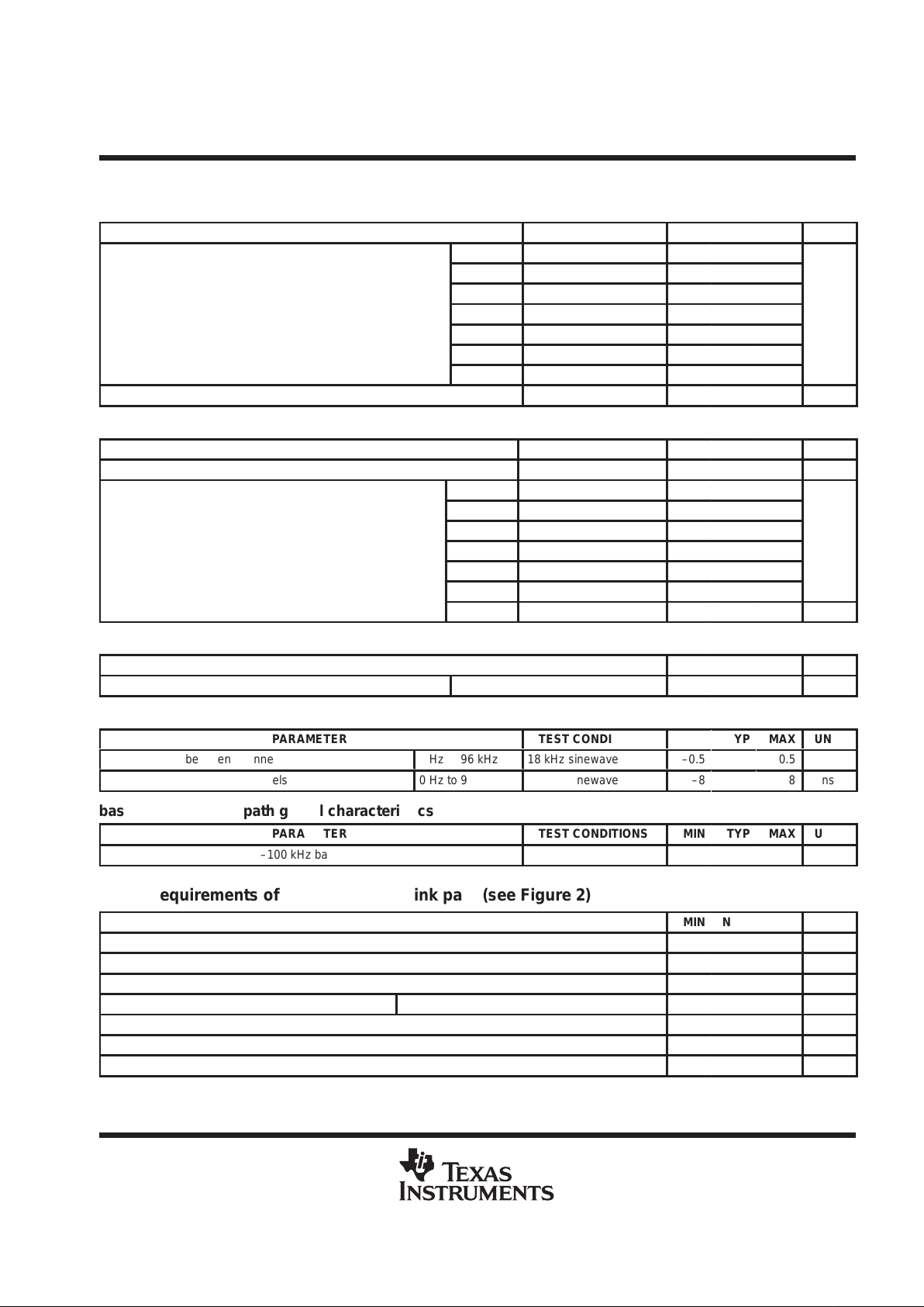
PARAMETER TEST CONDITIONS MIN TYP MAX UNIT
I and Q D/A converters resolution 8 bit
Dynamic range on each output Centered on V
VMID
V
VREF
Vpp
Differential output dynamic range with OUTLEV bit = 0
†
BULQP-BULQN or BULIP-BULIN 2xV
VREF
Vpp
Differential output dynamic range with OUTLEV bit = 1
†
BULQP-BULQN or BULIP-BULIN 8/15 x V
VREF
Vpp
Output load resistance, differential 10 kΩ
Output load capacitance, differential 50 pF
Output common-mode voltage Programmable by bit SELVMID V
VMID
V
I & Q output state in power down Hi-Z
†
Initial value after reset and at beginning of each burst are BULIP–BULIN=V
REF
and BULQP–BULQN=0 corresponding to a phase angle of 0°.
TCM4400E
GSM/DCS BASEBAND AND VOICE A/D
AND D/A RF INTERFACE CIRCUIT
SLWS082A – JULY 1999 – REVISED MARCH 2000
9
POST OFFICE BOX 655303 • DALLAS, TEXAS 75265
electrical characteristics over recommended operating free-air temperature range (unless
otherwise noted) (continued)
dc accuracy – baseband uplink path
PARAMETER MIN TYP MAX UNIT
Offset error before calibration
±100
mV
Offset error after calibration
†
–7
0
7
mV
†
Calibration must be performed in normal operation mode.
dynamic parameters – baseband uplink path
PARAMETER TEST CONDITIONS MIN TYP MAX UNIT
Absolute gain error relative to V
VREF
Measured with 67.7 kHz sinewave –1.5 0 1.5 dB
100 kHz –3 dB
200 kHz –34 dB
Maximum output random modulation spectrum relative to in-band
250 kHz –37 dB
average level. Measured by average
FFT
s of random bursts using
a
window with 30 kHz bandwidth.
400 kHz –65 dB
a window with 30 kHz bandwidth
.
600 KHz –72 dB
800 KHz –72 dB
smoothing filters characteristics – baseband uplink path
PARAMETER TEST CONDITIONS MIN TYP MAX UNIT
Group delay 0 Hz to 100 kHz 1.5 µs
I and Q channels gain matching – baseband uplink path
PARAMETER TEST CONDITIONS MIN TYP MAX UNIT
Gain matching between channels
0 Hz to 96 kHz
Measured on 67.7 kHZ sinewave
–1
0
1
dB
–0.42
–0.27
–0.12
I and Q gain unbalance
Programmable with bits IQSEL, G1, and G0
–0.68
–0.53
–0.38
dB
–0.93
–0.78
–0.63
baseband uplink path global characteristics
PARAMETER MIN TYP MAX UNIT
6° peak
GMSK ph
ase trajectory error
‡
1.5° rms
Power supply rejection 55 dB
‡
After software calibration through BBAloop
timing requirements of baseband uplink path
programmable delays – baseband uplink path (see Figure 1)
MIN NOM MAX UNIT
§
t
su1
Setup time, BENA before APC↑ Bits DELU of register BULRUDEL 0 15 1/4-bit
t
h1
Hold time, ramp-down from BENA low Bits DELD of register BULRUDEL 0 15 1/4-bit
Bit APCSPD = 0
1/16-bit
t
r
,
tfTransition time, APC
Bit APCSPD = 1
0
64
1/8-bit
§
Bit is relative to GSM bit = 1/270 kHz. Units can be a fractional part of the GSM bit as noted. Values in the above table are given for system
information only.
TCM4400E
GSM/DCS BASEBAND AND VOICE A/D
AND D/A RF INTERFACE CIRCUIT
SLWS082A – JULY 1999 – REVISED MARCH 2000
10
POST OFFICE BOX 655303 • DALLAS, TEXAS 75265
timing requirements of baseband uplink path (continued)
fixed delays – baseband uplink path (see Figure 1)
MIN NOM MAX UNIT
†
t
su2
Setup time, BULON↑ to BCAL↑ 15 µs
t
w1
Pulse duration, BCAL high 132 µs
t
su3
Setup time, BCAL low before BENA↑ 0 µs
t
w2
Pulse duration, BENA high N effective duration of burst controlled by BENA N–32 1/4-bit
t
h2
Hold time, modulation low after BENA low 32 1/4 bit
t
h3
Hold time, BULON↓ after APC low 1 bit
t
dd(mod)
Input-to-output modulator delay (Digital delay of modulator) 1.5 bit
†
Bit is relative to GSM bit = 1/270 kHz. Units can be a fractional part of the GSM bit as noted. Values in the above table are given for system
information only.
baseband downlink path
PARAMETER TEST CONDITIONS MIN TYP MAX UNIT
Dynamic range on each input
Centered on external common
mode (V
BDLCOM
)
V
VREF
Vpp
Differential input dynamic range DLQP–DLQN or DLIP–DLIN 2*V
VREF
Vpp
Differential input resistance at BDLQP–BDLQN or
BDLIP–BDLIN
130 200 270 kΩ
Differential input capacitance at BDLQP–BDLQN or
BDLIP–BDLIN
1.5 4 6.5 pF
Single ended input resistance at BDLQPor BDLQN or BDLIP
or BDLIN to ground.
90 130 180 kΩ
Single ended input capacitance at BDLQP or BDLQN or
BDLIP or BDLIN to ground.
6 8 12 pF
External common-mode input voltage: V
BDLCOM
0.8 VDD/2 VDD–0.8 V
Range of digital output data
Maximum digital code value on
16-bit I and Q samples.
±21060
dc accuracy – baseband downlink path
PARAMETER TEST CONDITIONS MIN TYP MAX UNIT
Offset error before calibration
‡
–60 0 60 LSB
Offset error after calibration, ± 21 on 16-bit I and Q words
‡
–2 0 2 LSB
Offset correction range Full scale
‡
The LSB corresponds to the one of the ADC which is specified with 66 dB dynamic range (±1024),which means 11-bit, but the output data bits
are transmitted through the serial interface with 16-bit words. On top of that, the decimation ratio of 24 (6.5 MHz/270 kHz) makes the maximum
code on a 16-bit word to be 21060 instead of 32767. So one LSB of the ADC corresponds to a value of 21060/1024 = 20.57 on the 16-bit output
serial words on I and Q.
channel characteristics
frequency response – baseband downlink path
PARAMETER MIN TYP MAX UNIT
< 67.5 Hz –0.3 0.25
67.5 kHz –0.3 0.25
p
p
96 kHz –4 0.3
Frequency response of the total path with values referenced to 18 kH
z
135 kHz –40
dB
200 kHz –40
400 kHz –40
TCM4400E
GSM/DCS BASEBAND AND VOICE A/D
AND D/A RF INTERFACE CIRCUIT
SLWS082A – JULY 1999 – REVISED MARCH 2000
11
POST OFFICE BOX 655303 • DALLAS, TEXAS 75265
channel characteristics (continued)
SNR vs signal level–baseband downlink path
PARAMETER TEST CONDITIONS MIN TYP MAX UNIT
–50 dBm0 200 kHz bandwidth 21
–40 dBm0 26
–30 dBm0 36
Signal level
–20 dBm0 46
dB
–10 dBm0 50
–5 dBm0 55
0 dBm0 30
Idle channel noise, 0 Hz –200 kHz –66 dBm0
gain characteristics of the baseband downlink path
PARAMETER TEST CONDITIONS MIN TYP MAX UNIT
Absolute gain error relative to V
VREF
at –10 dBm0 and 18 kHz –11 –10 –9 dB
0 dBm0 –0.25 0.25
–5 dBm0 –0.25 0.25
–10 dBm0 Reference level 0
Gain t
racking error. Over the range 3 dBm0 to –50 dBm0 at
–
–20 dBm0 –0.25 0.25
dB
18 kHz with reference 10 dBm0
–30 dBm0 –0.25 0.25
–40 dBm0 –0.25 0.25
–50 dBm0 –0.50 0.50 dB
group delay – baseband downlink path
PARAMETER MIN TYP MAX UNIT
Group delay 0 Hz to 100 kHz 28 µs
I and Q channels matching – baseband downlink path
PARAMETER
TEST CONDITIONS
MIN
TYP
MAX
UNIT
Gain matching between channels
0 Hz to 96 kHz
18 kHz sinewave
–0.5
0.5
dB
Delay matching between channels
0 Hz to 96 kHz
18 kHz sinewave
–8
8
ns
baseband downlink path global characteristics
PARAMETER TEST CONDITIONS MIN TYP MAX UNIT
Power supply rejection, 0 Hz –100 kHz band 70 dB
timing requirements of baseband downlink path (see Figure 2)
MIN NOM MAX UNIT
†
t
su4
Setup time, BDLON↑ to BCAL↑ 5 µs
t
w3
Pulse duration, BCAL 60 µs
t
su5
Setup time BCAL low before BENA↑ 0 µs
t
w4
Pulse duration, BENA high N ef fective duration of burst controlled by BENA N 1/4-bit
t
su6
Setup time, BENA↑ before DATAOUT V ALID 24.3 28 µs
t
h4
Hold time, DATAOUT VALID after BENA↓ 3.7 µs
t
h5
Hold time, BDLON low after BENA low 0 µs
†
Values in the above table are given for system information only.
TCM4400E
GSM/DCS BASEBAND AND VOICE A/D
AND D/A RF INTERFACE CIRCUIT
SLWS082A – JULY 1999 – REVISED MARCH 2000
12
POST OFFICE BOX 655303 • DALLAS, TEXAS 75265
automatic power control (APC)
APC level (8-bit DAC)
PARAMETER TEST CONDITIONS MIN TYP MAX UNIT
Integral nonlinearity (best fitting)
p
p
–1 1
Differential nonlinearity
Shaper at maximum full scale Load 10 kΩ, 50 pF
–1 1
LSB
Settling time 10 µs
APC shaper (5-bit DAC)
PARAMETER TEST CONDITIONS MIN TYP MAX UNIT
Integral nonlinearity (best fitting ) –1 1 LSB
Differential nonlinearity –1 1 LSB
Settling time
†
1 µs
†
Value given for system information only.
APC output stage
PARAMETER TEST CONDITIONS MIN TYP MAX UNIT
Output voltage at shape=31 & level =255 2.0 2.2 2.4 V
Output voltage at shape=0 & level=xx Bit APCMODE = 0 0 20 mV
Output voltage at shape=0 & level =xx Bit APCMODE =1 80 120 160 mV
Output voltage at shape=xx & level = 0 0 5 mV
Output voltage in power-down 0 V
DC power supply sensitivity 1%
Output impedance in power-down 20 Ω
Load resistance 10 kΩ
Load capacitance 50 pF
monitoring ADC
10-bit ADC
PARAMETER TEST CONDITIONS MIN TYP MAX UNIT
Integral nonlinearity (Best fitting) Input signal range < 0.95 V
VREF
–4 4 LSB
Differential nonlinearity Input signal range < 0.95 V
VREF
–2 2 LSB
Conversion time
†
10 µs
Input range 0 V
VREF
V
Input leakage current –10 10 µA
Input capacitance 25 pF
†
Value given for system information only.
TCM4400E
GSM/DCS BASEBAND AND VOICE A/D
AND D/A RF INTERFACE CIRCUIT
SLWS082A – JULY 1999 – REVISED MARCH 2000
13
POST OFFICE BOX 655303 • DALLAS, TEXAS 75265
automatic Gain Control (AGC)
AGC 10-bit DAC
PARAMETER TEST CONDITIONS MIN TYP MAX UNIT
Integral nonlinearity Best fitting line –1 1 LSB
Differential nonlinearity –1 1 LSB
Settling time From AUXAGC load 100 µs
AGC output stage
PARAMETER TEST CONDITIONS MIN TYP MAX UNIT
Output voltage with code max 1.9 2.2 2.4 V
Offset voltage with code 000 0.18 0.24 0.30 V
Output voltage in power down 0 V
DC power supply sensitivity 1%
Output impedance in power down 200 kΩ
Load resistance 10 kΩ
Load capacitance 50 pF
automatic frequency control (AFC)
AFC 13-bit DAC
PARAMETER TEST CONDITIONS MIN TYP MAX UNIT
AFCCK1=1 AFCCK0 = 1 2
p
AFCCK1=1 AFCCK0 = 0 1
Sampling frequenc
y,
f
s
AFCCK1=0 AFCCK0 = 1 0.5
MH
z
AFCCK1=0 AFCCK0 = 0 0.25
Integral nonlinearity from 0 to 75% output range Best fitting line ±1 LSB
Differential nonlinearity from 0 to 75% output range ±1 LSB
Settling time 1 µs
DC power-supply sensitivity Over power supply range 1%
AFC output stage
PARAMETER TEST CONDITIONS MIN TYP MAX UNIT
Internal output resistance (±30 % tolerance) 25 kΩ
External filtering capacitance 33 nF
Output voltage with code max 2.0 2.5 2.8 V
Output voltage with code min 0 3 6 mV
Output voltage in power down 0 V
p
p
p
Output impedance in power down
25
kΩ
TCM4400E
GSM/DCS BASEBAND AND VOICE A/D
AND D/A RF INTERFACE CIRCUIT
SLWS082A – JULY 1999 – REVISED MARCH 2000
14
POST OFFICE BOX 655303 • DALLAS, TEXAS 75265
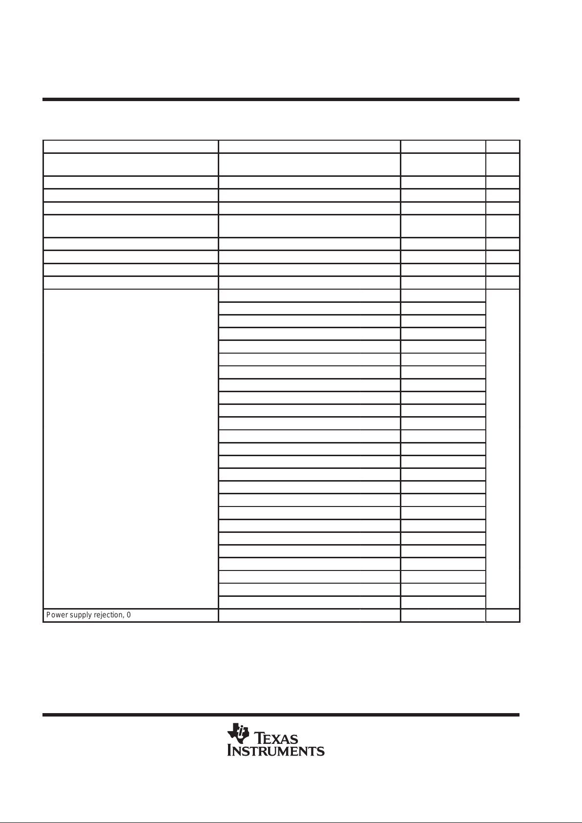
voice uplink path
global characteristics of voice uplink path
PARAMETER TEST CONDITIONS MIN TYP MAX UNIT
Maximum input range (MICP – MICN)
Inputs 3 dBm0 (maximum digital sample amplitude)
with PGA gain, set to 0dB (default value)
32.5 mVrms
Nominal reference level (MICP – MICN) –10 dBm0
Differential input resistance (MICP – MICN) 90 140 200 kΩ
Micro-amplifier gain 27 dB
Maximum input range at AUXI
Inputs 3 dBm0 (maximum digital sample amplitude)
with PGA gain, set to 0dB (default value)
365 mVrms
Nominal reference level at AUXI –10 dBm0
Input resistance at AUXI 140 220 300 kΩ
Auxi amplifier gain 6 dB
PGA absolute gain 4.6 dB
VULPGA code =10000 –12 dB –12.7 –12.2 –1 1.7
VULPGA code = 10111 –11 dB –11.3 –10.8 –10.3
VULPGA code = 11000 –10 dB –10.6 –10.1 –9.6
VULPGA code = 11001 –9 dB –9.5 –9 –8.5
VULPGA code = 11010 –8 dB –8.5 –8 –7.5
VULPGA code = 11011 –7 dB –7.5 –7 –6.5
VULPGA code = 00000 (default) –6 dB –6.7 –6.2 –5.7
VULPGA code = 00001 –5 dB –5.6 –5.1 –4.6
VULPGA code = 00010 –4 dB –4.6 –4.1 –3.6
VULPGA code = 00011 –3 dB –3.5 –3 –2.5
VULPGA code = 00100 –2 dB –2.4 –1.9 –1.4
VULPGA code = 00101 –1 dB –1.5 –1 –0.5
PGA gain step
VULPGA code = 00110 (ref) 0 dB 0
dB
VULPGA code = 00111 1 dB 0.7 1.2 1.7
VULPGA code = 01000 2 dB 1.4 1.9 2.4
VULPGA code = 01001 3 dB 2.6 3.1 3.6
VULPGA code = 01010 4 dB 3.6 4.1 4.6
VULPGA code = 01011 5 dB 4.5 5 5.5
VULPGA code = 01100 6 dB 5.3 5.8 6.3
VULPGA code = 10001 7 dB 6.4 6.9 7.4
VULPGA code = 10010 8 dB 7.4 7.9 8.4
VULPGA code = 10011 9 dB 8.6 9.1 9.6
VULPGA code = 10100 10 dB 9.6 10.1 10.6
VULPGA code = 10101 11 dB 10.5 11 11.5
VULPGA code = 10110 12 dB 11.5 12 12.5
Power supply rejection, 0 Hz –100 kHz band
70
dB
TCM4400E
GSM/DCS BASEBAND AND VOICE A/D
AND D/A RF INTERFACE CIRCUIT
SLWS082A – JULY 1999 – REVISED MARCH 2000
15
POST OFFICE BOX 655303 • DALLAS, TEXAS 75265
voice uplink path (continued)
frequency response of the voiceband uplink path
PARAMETER
TEST CONDITIONS
MIN TYP MAX UNIT
100 Hz –37.4 –20
150 Hz –25.9 –15
200 Hz –16.5 –10
300 Hz –2 –1.46 1
1000 Hz Reference point is 1000 Hz 0
Frequency response (Gain relative to reference gain at
2000 Hz –1.5 –0.58 1
qy ( g
1 kHz)
3000 Hz –1.5 –0.77 1
dB
3400 Hz –2 –1 1
3600 Hz –12.4 –6
3800 Hz –23.3 –18
4000 Hz –35 –30
>4600 Hz >–52 –40
psophometric SNR vs signal level of the voiceband uplink path
PARAMETER TEST CONDITIONS MIN TYP MAX UNIT
3 dBm0 35
0 dBm0 40
–5 dBm0 42
–10 dBm0 45
Signal to noise
+
distortion
–20 dBm0 42
dB
–30 dBm0 40
–40 dBm0 30
–45 dBm0 25
Maximum idle channel noise 0 Hz –4 kHz –72 dBm0
Crosstalk with the downlink path Downlink path loaded with 150 Ω –66 dB
gain characteristics of the voiceband uplink path
PARAMETER TEST CONDITIONS MIN TYP MAX UNIT
at 0dBm0 and 1KHz –1 1
Absolute gain error
at –10dBm0 and 1KHz –1 1 –10 –9
dB
3 dBm0 –0.25 0.25
0 dBm0 –0.25 0.25
–5 dBm0 –0.25 0.25
Gain tracking error. Over the range 3 dBm0 to –45 dBm0 at
–10 dBm0 Reference level 0
gg
1 kHz with reference –10 dBm0
–20 dBm0 –0.25 0.25
dB
–30 dBm0 –0.25 0.25
–40 dBm0 –0.35 0.35
–45 dBm0 –0.50 0.50
TCM4400E
GSM/DCS BASEBAND AND VOICE A/D
AND D/A RF INTERFACE CIRCUIT
SLWS082A – JULY 1999 – REVISED MARCH 2000
16
POST OFFICE BOX 655303 • DALLAS, TEXAS 75265
voice downlink path
global characteristics of voice downlink path
PARAMETER TEST CONDITIONS MIN TYP MAX UNIT
Maximum output swin
g
With 5% distortion and with 150 Ω 3.1 3.92
pp
Maximum out ut swing
(EARP – EARN)
With 5% distortion and with 33 Ω 1.2 1.5
Vpp
p
Output swing 3.9Vpp 120 150 Ω
Minimum output resistive load at EARP_EARN
Output swing 1.5Vpp 30 33 Ω
Maximum output capacitive load at EARP_EARN 100 pF
Earphone amplifier gain 0 dB
Earphone amplifier state in power down Hi-Z
Maximum output swing (AUXO), 5% distortion, maximum Load = 1 kΩ 1.6 1.96 Vpeak
Minimum output resistive load at AUXO AC coupled 1.0 1.2 kΩ
Maximum output capacitive load at AUXO 100 pF
Auxo amplifier gain –6 dB
Auxo amplifier state in power down Hi-Z
VOLCTL code = 010 –1 0 1
VOLCTL code = 110 –7 –6 –5
VOLCTL code = 000 (default & reference) –12
Volume control gains
VOLCTL code = 100 –19 –18 –17
dB
VOLCTL code = 011 –25 –24 –23
VOLCTL code =101 or 001 or 111 (mute) –40
VDLPGA code = 0000 (default) –6 dB –6.5 –6.0 –5.5
VDLPGA code = 0001 –5 dB –5.5 –5.0 –4.5
VDLPGA code = 0010 –4 dB –4.5 –4.0 –3.5
VDLPGA code = 0011 –3 dB –3.7 –3.2 –2.7
VDLPGA code = 0100 –2 dB –2.3 –1.8 –1.3
VDLPGA code = 0101 –1 dB –1.7 –1.2 –0.7
PGA gain steps
VDLPGA code = 0110 (ref.) 0 dB 0
dB
VDLPGA code = 0111 1 dB 0.5 1.0 1.5
VDLPGA code = 1000 2 dB 1.4 1.9 2.4
VDLPGA code = 1001 3 dB 2.6 3.1 3.6
VDLPGA code = 1010 4 dB 3.4 3.9 4.4
VDLPGA code = 1011 5 dB 4.3 4.8 5.3
VDLPGA code = 1100 6 dB 5.5 6.0 6.5
VDLST code = 1101 –23 dB –24.6 –24.1 –22.6
VDLST code = 1100 –20 dB –21.1 –20.6 –18.5
VDLST code = 0110 –17 dB –18.3 –17.8 –17.3
VDLST code = 0010 –14 dB –14.8 –14.3 –13.8
p
VDLST code = 0111 –11 dB –12.3 –11.8 –11.3
Sidetone gain steps
VDLST code = 0011 –8 dB –8.8 –8.3 –7.8
dB
VDLST code = 0000 (ref.) –5 dB –5.9 –4.8 –4.3
VDLST code = 0100 –2 dB –2.1 –1.6 –1.1
VDLST code = 0001 1 dB 0.7 1.2 1.7
VDLST code = 1000 Mute –55 –50
Power supply rejection, 0 Hz –100 kHz In the band 60 dB
NOTE: All parameters are given for a 150 Ω load, unless specified.
TCM4400E
GSM/DCS BASEBAND AND VOICE A/D
AND D/A RF INTERFACE CIRCUIT
SLWS082A – JULY 1999 – REVISED MARCH 2000
17
POST OFFICE BOX 655303 • DALLAS, TEXAS 75265
voice downlink path (continued)
frequency response of the voiceband downlink path
PARAMETER TEST CONDITIONS MIN TYP MAX UNIT
100 Hz –5.8 –5
150 Hz
–3.6 –2
200 Hz –2.5 1
300 Hz –3 –1.4 1
1000 Hz Reference point 0
Frequency response (Gain relative to
2000 Hz –1 –0.6 1
qy (
reference gain at 1 kHz)
3000 Hz –1 –0.15 1
dB
3400 Hz –3 –0.35 1
3600 Hz
–9.0 –6
3800 Hz
–21.0 –15
4000 Hz –32.0 –28
>4600 Hz –60.0
psophometric SNR vs signal level of the voiceband downlink path
PARAMETER TEST CONDITIONS MIN TYP MAX UNIT
–45 dBm0 25
–40 dBm0 30
–30 dBm0 40
–20 dBm0 42
Si
gnal leve
l
–10 dBm0 45
dB
–5 dBm0 42
0 dBm0
40
3 dBm0 35
Idle channel noise, 0 Hz –4 kHz –71 dBm
Crosstalk with the uplink path –50 dB
gain characteristics of the voiceband downlink path
PARAMETER TEST CONDITIONS MIN TYP MAX UNIT
at 0 dbm0 and 1 kHz –1.8 0 0.2
Absolute gain error
at –10 dbm0 and 1 kHz –11.8 –10 –9.8
dB
3 dBm0 –0.25 0.25
0 dBm0 –0.25 0.25
–5 dBm0 –0.25 0.25
Gain tracking error. Over the range 3 dBm0 to –45 dBm0 at
–10 dBm0 Reference level 0
1 kHz with reference –10 dBm0 PGA gain
=
0dB. Volume
control = –12 dB
–20 dBm0 –0.25 0.25
dB
control 12 dB
–30 dBm0 –0.25 0.25
–40 dBm0 –0.35 0.35
–45 dBm0 –0.50 0.50
TCM4400E
GSM/DCS BASEBAND AND VOICE A/D
AND D/A RF INTERFACE CIRCUIT
SLWS082A – JULY 1999 – REVISED MARCH 2000
18
POST OFFICE BOX 655303 • DALLAS, TEXAS 75265
power consumption
consumption by circuit block
CIRCUIT BLOCK TEST CONDITIONS MIN TYP MAX UNIT
ADC
DVDD3 0.013
AFC
AVDD3 0.021
mA
AVDD5 0.027
AVDD3 0.054
AGC
AVDD5 0.683
mA
DVDD3 0.133
APC
AVDD3 0.108
mA
AVDD5 0.442
Auxiliary input stage AVDD4 2.240 mA
Auxiliary output stage A VDD4 1.550
Band gap AVDD1 0.163 mA
DVDD2 2.810
Baseband downlink
AVDD2 9.310
mA
p
DVDD2 0.460
Baseband uplink
AVDD2 4.910
mA
BBIF DVDD1 BDL Active 1.490 mA
Clock generator BBIF DVDD1 0.122 mA
Clock generator Idle DVDD1 0.204 mA
Clock generator TIIF DVDD1 0.181 mA
Clock generator VBIF DVDD1 0.144 mA
Digital modulator DVDD4 0.183 mA
Earphone output stage AVDD4 4.170 mA
Microphone input stage AVDD4 3.000 mA
DVDD4 1.380
Voiceband downlink
AVDD4 2.990
mA
p
DVDD4 1.200
Voiceband uplink
AVDD4 0.115
mA
current consumption for typical configurations
PARAMETER TEST CONDITIONS MIN TYP MAX UNIT
Deep power down
13-MHz clock applied; PWRDN active;
Band-gap voltage reference off
200 µA
Power down with AFC active AFC programmed with internal 50-kΩ and 1-MHz clock 0.7 1.1 mA
AFC + GMSK – Rx Paging 14 16 mA
Audio + GMSK – Tx + APC + AFC Transmit burst 19 21 mA
Audio + GMSK – Rx +AGC+ AFC Receive burst 27 30 mA
TCM4400E
GSM/DCS BASEBAND AND VOICE A/D
AND D/A RF INTERFACE CIRCUIT
SLWS082A – JULY 1999 – REVISED MARCH 2000
19
POST OFFICE BOX 655303 • DALLAS, TEXAS 75265
MCU serial interface timing requirements (see Figure 3)
PARAMETER MIN NOM MAX UNIT
t
su10
Setup time, UCLK stable before USEL↓ 20 ns
t
v1
Hold time, UDX valid after USEL↓ 20 ns
t
v2
Hold time, UDX valid after UCLK↑ 20 ns
t
h9
Sequential transfer delay between 16-bit word acquisition tw pulse duration, USEL high 3000 ns
t
h10
Hold time, UCLK↑ after USEL↓ 20 ns
t
h11
Hold time, UCLK unknown after USEL↑ 20 ns
t
su11
Setup time, data valid before UCLK↓ 20 ns
t
h12
Hold time, data valid after UCLK↓ 20 ns
t
c
Cycle time, ULCK 154 ns
DSP serial interface timing requirements (see Figure 4)
PARAMETER MIN NOM MAX UNIT
BCLKX BCLKX signal frequency ( Burst mode or Continuous mode depending on bit BCLKMODE) 13 MHz
BCLKX BCLKX duty cycle 40% 50% 60%
t
su12
Setup time, BFSX high before BCLKX ↓ 20 ns
t
h12
Hold time, BFSX high after BCLKX ↓ 20 ns
t
su13
Setup time, BDX valid before BCLKX ↓ 20 ns
t
h13
Hold time, BDX valid after BCLKX ↓ 20 ns
(Output BCLKDIR = 0) 4.33
BCLKR
BCLKR si
gnal frequency
(Input BCLKDIR = 1)
13
MH
z
BCLKR BCLKR duty cycle 40% 50% 60%
t
su14
Setup time, BFSR high before BCLKR ↓ 20 ns
t
h14
Hold time, BFSR high after BCLKR ↓ 20 ns
t
su16
Setup time, BDR valid before BCLKR ↓ 20 ns
t
h15
Setup time, BDR valid after BCLKR ↓ 20 ns
voice timing requirements (see Figure 5)
PARAMETER MIN NOM MAX UNIT
VCLK VCLK signal frequency ( Burst mode or Continuous mode depending on bit VCLKMODE) 520 kHz
VCLK VCLK duty cycle 40% 50% 60%
t
su7
Setup time, VFS high before VCLK ↓ 100 ns
t
h6
Hold time, VFS high after VCLK ↓ 100 ns
t
su8
Setup time, VDX valid before VCLK ↓ 100 ns
t
h8
Hold time, VDX valid after VCLK ↓ 100 ns
t
su9
Setup time, VDR valid before VCLK ↓ 100 ns
t
h7
Hold time, VDR valid after VCLK ↓ 100 ns
TCM4400E
GSM/DCS BASEBAND AND VOICE A/D
AND D/A RF INTERFACE CIRCUIT
SLWS082A – JULY 1999 – REVISED MARCH 2000
20
POST OFFICE BOX 655303 • DALLAS, TEXAS 75265
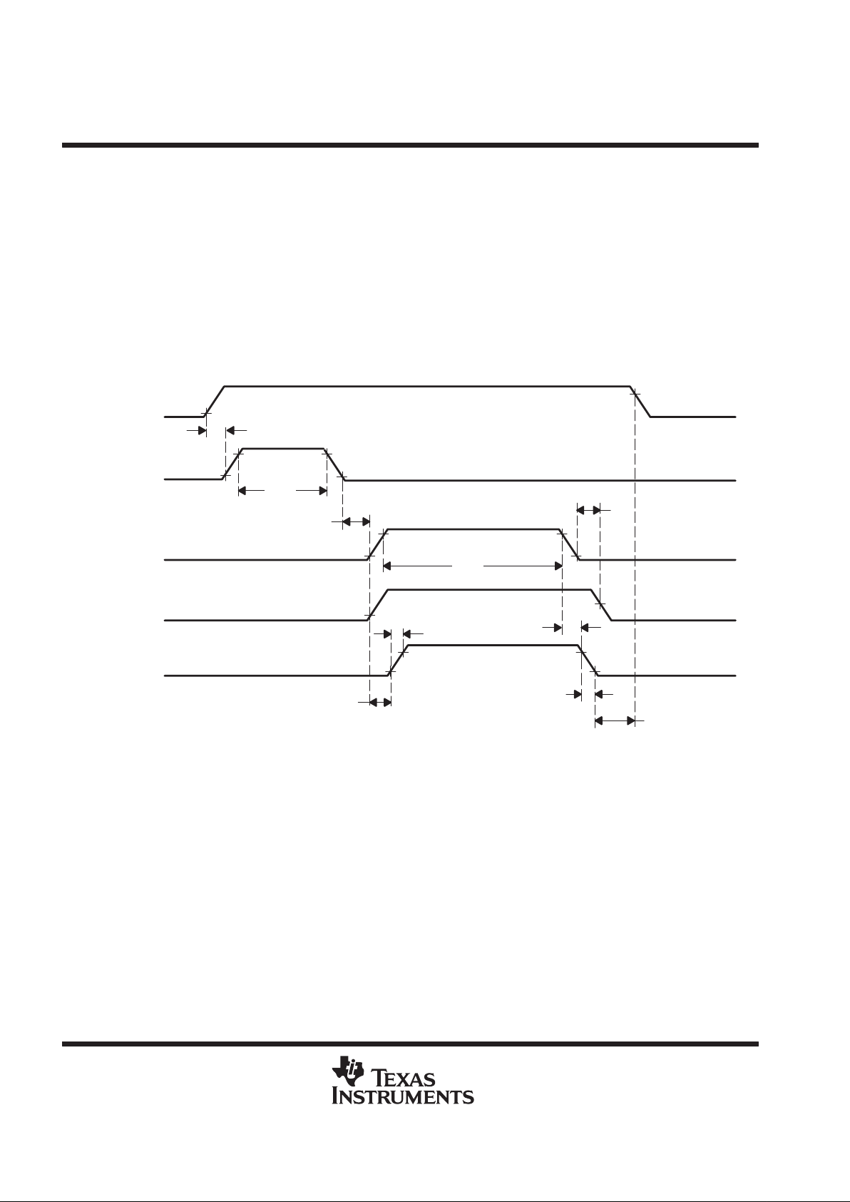
PARAMETER MEASUREMENT INFORMATION
uplink timing considerations
Figure 1 shows the timing diagram for the uplink operation.
Timing for power up, offset calibration, data transmission, and power ramp-up are driven by control bits applied
to BULON (base uplink on), BCAL (calibration) and BENA (enable). The burst content including guard bits, tail
bits, and data bits is sent by the DSP by way of the DSP interface and then stored by the TCM4400E in a burst
buffer. Transmission start is indicated by the control bit BENA when the BULON is active. The transmission,
sequencing, and power ramp-up are then controlled by an on-chip burst sequencer with a one-quarter-bit timing
accuracy. For a detailed description of the baseband in length path, see the functional description of the
baseband uplink path in the
Principles of Operation
section.
t
su2
t
w1
t
su3
t
h2
t
su1
t
r1
t
h1
t
f1
t
h3
BULON
BCAL
BENA
MODULATION
APC
t
w2
Figure 1. Uplink Timing Diagram

TCM4400E
GSM/DCS BASEBAND AND VOICE A/D
AND D/A RF INTERFACE CIRCUIT
SLWS082A – JULY 1999 – REVISED MARCH 2000
21
POST OFFICE BOX 655303 • DALLAS, TEXAS 75265
PARAMETER MEASUREMENT INFORMATION
downlink timing considerations
Figure 2 shows the timing diagram for downlink operation.
Timing control of the baseband downlink path is controlled by bits DLON (downlink on), BCAL (calibration) and
BENA (enable) when BDLON is active (see the topic, timing and interface). BDLON controls the power up of
the baseband downlink path, BCAL controls the start and duration of the autocalibration sequence, and BENA
controls the beginning and the duration of data transmission to the DSP, using the DSP serial interface.
The power-down sequence is controlled with two bits, the first bit (BBDL W of PWDNRG1 register) determines
whether the baseband downlink path can be powered down with external GSM receive window activation
(BDLON); the second bit (BBDLPD of PWDNRG1 register) controls the activation of the baseband downlink
path. See the topic,
power-down functional description
, for more details about power-down control.
t
w3
t
su6
BDLON
BCAL
DATAOUT
t
su4
t
su5
t
h4
t
h5
BENA
t
w4
Figure 2. Downlink Timing Sequence

TCM4400E
GSM/DCS BASEBAND AND VOICE A/D
AND D/A RF INTERFACE CIRCUIT
SLWS082A – JULY 1999 – REVISED MARCH 2000
22
POST OFFICE BOX 655303 • DALLAS, TEXAS 75265
PARAMETER MEASUREMENT INFORMATION
microcontroller serial interface timing considerations
Figure 3 shows the timing diagram for the microcontroller serial interface.
The microcontroller serial interface is designed to be compliant with 8-bit standard synchronous serial ports.
The microcontroller operates on 16-bit words; this interface consists of four pins.
UCLK: A clock provided by the microcontroller to control access to baseband, voiceband, and auxiliary
functions registers
UDR: An input terminal to control read and write access to baseband, voiceband, and auxiliary functions
registers
UDX: An output terminal to transmit data from read access of baseband, voiceband, and auxiliary
functions registers
USEL: An input terminal to enable read and write access to baseband, voiceband, and auxiliary functions
registers through the microcontroller interface
ÏÏÏ
t
su10
t
h10
t
c
t
su11
t
h10
t
v2
t
h11
t
h9
t
v1
t
h12
Hi-Z Hi-Z
USEL
UCLK
UDR
UDX
Figure 3. Microcontroller Serial Interface Timing Waveforms
(Mode Rising Edge Without Delay)

TCM4400E
GSM/DCS BASEBAND AND VOICE A/D
AND D/A RF INTERFACE CIRCUIT
SLWS082A – JULY 1999 – REVISED MARCH 2000
23
POST OFFICE BOX 655303 • DALLAS, TEXAS 75265
PARAMETER MEASUREMENT INFORMATION
DSP serial port timing considerations
Figure 4 shows the timing diagram for DSP serial port operation.
Six pins are used for the serial port interface; see Figure 14. The terminal BCLKR is an I/O port for the serial
clock used to control the reception of the data BDR. At reset BCLKR is configured as an output and the clock
frequency is set to MCLK/3 (4.333 MHz with MCLK = 13 MHz); the clock signal is running permanently . The port
BCLKR can be reconfigured as an input by programming an internal register. In this case BCLKR is provided
by the DSP and can run in burst mode to reduce power consumption. The receive frame synchronization (BFSR)
identifies the beginning of a data packet transfer on port BDR.
The transmitted serial data (BDX) is the serial data input; the transmit frame synchronization (BFSX) is used
to initiate the transmission of data. The transmit clock (BCLKX) is provided by the GSM baseband and voice
A/D and D/A converters with a frequency of MCLK. The downlink data bus (BFSX, BCLKX, BDX) can be driven
to VSS or placed in high-impedance when no data is to be transferred to the DSP. The bit BCLKDIR of the
register BCTLREG controls the direction of the BCLKR clock.
Similar to the voice serial interface, an extra clock cycle must be generated, since the last 16-bit word received
on the DSP serial interface is latched on the next two falling BCLKR edges, following the least significant bit
(LSB). As for the voice serial interface, one extra clock period is generated on the BCLKX before the first
synchronization BFSX of downlink data sequence.
BCLKX
t
su12
t
h13
t
su13
t
h14
BFSX
BDX
A15
A14 A13 A12 A3 A2 A1 A0
MSB LSB
a. Burst-Mode Serial-Port Transmit Operation
t
su14
t
h14
t
su15
t
h15
BDR A15 A14 A13 A12 A3 A2 A1 A0
MSB LSB
b. Burst-Mode Serial-Port Receive Operation
B15 B14 B13
BCLKR
BFSR
Figure 4. DSP Serial Port Timings

TCM4400E
GSM/DCS BASEBAND AND VOICE A/D
AND D/A RF INTERFACE CIRCUIT
SLWS082A – JULY 1999 – REVISED MARCH 2000
24
POST OFFICE BOX 655303 • DALLAS, TEXAS 75265
PARAMETER MEASUREMENT INFORMATION
voiceband serial interface timing considerations
Figure 5 shows the timing diagram for both transmit and receive voiceband serial interface operation.
The signal VCLK is the output serial clock used to control the transmission or reception of the data (see
Figure 5). The transmitted serial data (VDX) is the serial data output; the frame synchronization (VFS) is used
to initiate the transfer of transmit and receive data. The received data (VDR) is the serial data input.
Each serial port includes four registers that include the data transmit register (DXR), the data receive register
(DRR), the transmit shift register (XSR), and the receive shift register (RSR).
The voice serial interface has the same structure and timing diagram as the serial interface; one extra cycle is
generated before VFS, and two extra cycles are generated after the LSB.
XLOAD and RLOAD are internal signals.
VCLK
t
su7
t
h6
t
su8
t
h8
VFS
VDX
XLOAD
A15 A14 A13 A12 A3 A2 A1 A0
MSB LSB
DXR
Loaded
XSR
Loaded
a. Audio-Serial-Port Transmit Operation
VCLK
t
su9
t
h7
VFS
VDR
RLOAD
A15 A14 A13 A12 A3 A2 A1 A0
MSB LSB
DDR
Loaded
b. Audio-Serial-Port Receive Operation
Figure 5. Voiceband Serial Interface Timing Waveforms

TCM4400E
GSM/DCS BASEBAND AND VOICE A/D
AND D/A RF INTERFACE CIRCUIT
SLWS082A – JULY 1999 – REVISED MARCH 2000
25
POST OFFICE BOX 655303 • DALLAS, TEXAS 75265
PRINCIPLE OF OPERATION
baseband uplink path
Traditional transmit and receive terms can be confusing when describing a cellular telephone two-way
communication. This document uses the terms
uplink
, meaning from a user device to a remote station, and
downlink
meaning from a remote station, whether earthbound or satellite, to indicate the signal-flow direction.
The modulator circuit in the baseband uplink path performs the Gaussian minimum shift keying (GMSK) in
accordance with the GSM specification 5.04. The data to be modulated flows from the DSP through the serial
interface, it is differentially encoded, and it is applied to the input of the GMSK modulator . The GMSK modulator,
implemented with digital logic and a sin/cos look-up table in ROM, generates the I and Q components (words)
with an interpolation ratio of 16.
These digital I and Q words are sampled at a 4.33 MHz rate and applied to the inputs of a pair of high-speed
8-bit DACs. The analog outputs are then processed by third-order Bessel filters to reduce image frequencies
due to sampling and to obtain a spectrum consistent with GSM specification 05.05 (see Figure 6).
NOTE A: Conformance with GSM Rec 05.05: simulated spectrum of an infinite modulation of random data with a Blackman
Harris analysis window.
MAGNITUDE
Frequency – MHz
MAGNITUDE
vs
FREQUENCY
0
–20
–40
–60
–80
–100
–120
01062×1063×1064×1065×1066×10
6
Figure 6. Typical GSM Modulation Spectrum
Full-differential buffered signals are available at ULIP, ULIN, ULQP, and ULQN. These signals are suitable for
use in the RF circuit for generating a phase-modulated signal of the form:
s(t) = A Cos (2 Pi fc t + Phi (t, alpha))
where fc is the RF carrier frequency, and Phi (t, alpha) is the phase component generated by the GMSK
modulator from the differential encoded data.

TCM4400E
GSM/DCS BASEBAND AND VOICE A/D
AND D/A RF INTERFACE CIRCUIT
SLWS082A – JULY 1999 – REVISED MARCH 2000
26
POST OFFICE BOX 655303 • DALLAS, TEXAS 75265
PRINCIPLES OF OPERATION
baseband uplink path (continued)
Timing for power up, offset calibration, data transmission, and power ramp-up is driven by control bits applied
to BULON (base uplink on), BCAL (calibration) and BENA (enable) (see Figure 1). The entire content of a burst,
including guard bits, tail bits, and data bits, is sent by the DSP using the DSP interface and then stored by the
TCM4400E in a burst buffer . Transmission start is indicated by the control bit BENA when the BULON is active.
The transmission, sequencing, and power ramp-up are then controlled by an on-chip burst timing control circuit
having a one-quarter-bit timing accuracy (see Figure 7). All data related to a burst to be transmitted, such as
bit data, ramp-up & ramp-down delay programmation, have to be loaded before the rising edge of BENA.
The burst length is determined by the time during which the BENA signal is active. Effective burst length is equal
to the duration of BENA + 32 one-quarter bits. The tail of the burst is controlled internally , which means that the
modulation is maintained for 32 one-quarter bits after BENA turns off to generate the ramp-down sequence and
complete modulation.
For each burst, the power control level can be controlled by using the serial interfaces to write the power level
value into the power register of the auxiliary RF power control circuitry. The power ramp-up and ramp-down
sequences are controlled by the burst sequencer, while the shape of the power control is generated internally
by dedicated circuitry, which drives the power control 5-bit and 8-bit D/A converters.
T o minimize phase error , the I and Q channel dc of fset can be minimized using offset calibration. Each channel
includes an offset register in which a value corresponding to the required dc offset is stored, controlling the dc
offset of the I channel and Q channel D/A converters. This value is set by a calibration sequence. Starting and
stopping the calibration sequence is controlled by the control bit BCAL using the timing interface when BULON
is active. During the calibration sequence, the digital value of I and Q is forced to zero so that only the offset
register value drives the D/A converters, and a low-offset comparator senses the dc level at the BULIP/BULIN
and BULQP/BULQN outputs and modifies the content of the offset registers to minimize the dc offset (see
Figure 7).
Gain unbalance can be introduced between I and Q channels to allow compensation of imperfections in RF
circuits. This gain unbalance is controlled through the mean of three program bits: IQSEL,G1, and G0 of
baseband uplink register BULCTL.
The power-down function is controlled with two bits. The first bit (BBULW of the PWDNRG1 register),
determines whether the baseband uplink path can be powered down with external GSM transmit window
activation (BULON). The second bit (BBULPD of the PWDNREG1 register) controls the activation of the
baseband uplink path. For more details about power-down control, see the
power-down functional description
section.

TCM4400E
GSM/DCS BASEBAND AND VOICE A/D
AND D/A RF INTERFACE CIRCUIT
SLWS082A – JULY 1999 – REVISED MARCH 2000
27
POST OFFICE BOX 655303 • DALLAS, TEXAS 75265
PRINCIPLES OF OPERATION
baseband uplink path (continued)
Burst
Register
Din
270 kHz
Differential
Encoder
Gaussian
Filter
Integrator
Power
Register
Ramp-Up
Shaper
Cosine
Table
8-Bit
DAC
Low-Pass
Filter
Sine
Table
Low-Pass
Filter
fs = 16 x 270 kHz
8-Bit
DAC
Offset
Register
Offset
Register
BULIP
BULIN
BULQP
BULQN
To Power
Control DAC
Burst Timing
Control
Timing Interface
–
–
+
+
I/Q Gain Unbalance
Figure 7. Functional Structure of the Baseband Uplink Path
baseband downlink path
The baseband downlink path includes two identical circuits for processing the baseband I and Q components
generated by the RF circuits. The first stage of the downlink path is a continuous-time second-order antialiasing
filter (see Figure 8) that prevents aliasing due to sampling in the A/D converter. This filter also serves as an
adaptation stage (input impedance and common-mode level) between external-world and on-chip circuitry.
Magnitude – dB
TYPICAL FREQUENCY RESPONSE OF THE
ANTIALIASING FILTER
10
0
–10
–20
–30
–40
–50
–60
–70
f – Frequency – Hz
10
2
10
3
10
4
10
5
10
6
10
7
Figure 8. Antialiasing Filter

TCM4400E
GSM/DCS BASEBAND AND VOICE A/D
AND D/A RF INTERFACE CIRCUIT
SLWS082A – JULY 1999 – REVISED MARCH 2000
28
POST OFFICE BOX 655303 • DALLAS, TEXAS 75265
PRINCIPLES OF OPERATION
baseband downlink path (continued)
The antialiasing filter is followed by a third-order sigma-delta modulator that performs A/D conversion at a
sampling rate of 6.5 MHz. The A/D converter provides 3-bit words that are fed to a digital filter (see Figure 9)
that performs the decimation by a ratio of 24 to lower the sampling rate down to 270.8 KHz and the channel
separation by rejecting enough of the adjacent channels to allow the demodulation performances required by
the GSM specification. Figure 10 shows the frequency response curve for the downlink digital filter and Figure
11 shows the in-band response curve for the same digital filter.
The baseband downlink path includes an offset register in which the value representing the channel dc offset
is stored; this value is subtracted from the output of the digital filter before transmitting the digital samples to
the DSP using the serial interface. Upon reset, the offset register is loaded with 0 and updated with the BCAL
calibrating signal (see Figure 2).
The content of the offset register results from a calibration sequence. The input BDLIP is shorted with the input
BDLIN, and the input BDLQP is shorted with the input BDLQN. The digital outputs are evaluated and the values
are stored in the corresponding offset registers in accordance with the dc offset of the GSM baseband and voice
A/D and D/A downlink path. When the external autocalibration sequence is selected, the inputs BDLIP and
BDLIN and the inputs BDLQP and BDLQN remain connected to the external circuitry. The digital outputs are
evaluated, and the values stored in the corresponding offset registers take into account the dc offset of the
external circuitry.
Timing control of the baseband downlink path is controlled by bits BDLON (downlink on), BCAL (calibration),
and BENA (enable) when BDLON is active (please see
timing interface
section). BDLON controls the power
up of the baseband downlink path; BCAL controls the start and duration of the autocalibration sequence (which
can be internal or external depending on bit EXTCAL of PWDNRG1 register); and BENA controls the beginning
and the duration of data transmission to the DSP by using the DSP serial interface. To avoid transmission of
irrelevant data corresponding to the settling time of the digital filter, the eight first I&Q computed samples are
not sent to the DSP; first data are transmitted though the DSP interface about 30 µs after the BENA rising edge.
The power-down sequence is controlled with two bits. The first bit (BBDL W of PWDNRG1 register) determines
whether the baseband downlink path can be powered down with external GSM receive window activation
(BDLON): The second bit, BBDLPD of register PWDNRG1, controls the activation of the baseband downlink
path. Please see
power-down functional description
section for more details about power-down control.
Antialiasing
Filter
Sigma-Delta
Modulator
SINC
Filter
Sigma-Delta
Modulator
SINC
Filter
FIR
Filter
FIR
Filter
Offset
Calibration
Offset
Register
SUB
Offset
Calibration
Offset
Register
SUB
Antialiasing
Filter
fs3 = 270.8 kHz
fs2 = 1.08 MHzfs1 = 6.5 MHz
BDLIP
BDLIN
BDLQP
BDLQN
To Baseband
Serial Interface
Figure 9. Functional Structure of the Baseband Downlink Path

TCM4400E
GSM/DCS BASEBAND AND VOICE A/D
AND D/A RF INTERFACE CIRCUIT
SLWS082A – JULY 1999 – REVISED MARCH 2000
29
POST OFFICE BOX 655303 • DALLAS, TEXAS 75265
PRINCIPLES OF OPERATION
baseband downlink path (continued)
10
0
–10
–20
–30
–40
–50
–60
–70
–80
0 50 100 150 200
f – Frequency – kHz
Magnitude – dB
Figure 10. Downlink Digital Filter Frequency Response
0.4
0.2
0
–0.2
–0.4
010203040
f – Frequency – kHz
Magnitude – dB
50 60 70 80
Figure 11. Downlink Digital Filter In-Band Response

TCM4400E
GSM/DCS BASEBAND AND VOICE A/D
AND D/A RF INTERFACE CIRCUIT
SLWS082A – JULY 1999 – REVISED MARCH 2000
30
POST OFFICE BOX 655303 • DALLAS, TEXAS 75265
PRINCIPLES OF OPERATION
auxiliary RF functions
The auxiliary RF functions include the following:
D
Automatic frequency control
D
Auxiliary analog converter (Automatic gain control)
D
RF power control
D
Monitoring
Each of these functions is discussed in the following paragraphs.
automatic frequency control (AFC)
The automatic frequency control function consists of a DAC converter optimized for high-resolution dc
conversion. The AFC digital interface includes two registers that can be written using the serial interfaces. The
content of these registers controls a 13-bit DAC, whose purpose is to correct frequency shifts of the oscillator
maintaining the master clock frequency in a 0.1 ppm range.
Optimizing the AFC function depends on the type of oscillator used and whether its sampling frequency is
programmable. This means that the lower the selected frequency the lower the resolution and power
consumption. Using a high-quality resonance oscillator filter permits the AFC circuit to operate at low frequency .
Thus, a low-cost oscillator permits operation at a higher internal frequency to ensure 13-bit resolution.
The AFC value is programmed with registers AUXAFC1, which contains the ten LSBs, and AUXAFC2, which
contains the three MSBs. The three MSBs are sent to the DAC through a shadow register the contents of which
is updated when LSBs are written in AUXAFC1, so proper operation of the AFC is ensured by writing the MSB’s
first and then the LSBs.
Internal resistance and output voltage swing selection are controlled with bit AFZ of AUXCTL2 register. Power
down is controlled with two bits: the first bit, AFCPN of AUXCTL1 register, determines whether the AFC can be
powered down from the external PWRDN terminal; the second bit, AFCPD of AUXCTL1 register, controls the
activation of the the AFC function. See the topic, power-down functional description for more details about
power-down control.
The auxiliary analog functions of the GSM baseband A/D and D/A conversions are independently powered from
the AV
DD5
external terminal.
auxiliary analog converter (automatic gain control (AGC))
The auxiliary analog converter control function includes a register which can be written to using the serial
interfaces and a 10-bit D/A converter that provides a control signal to set the gain of the RF section receive
amplifier. The 10-bit D/A converter is accessed through the internal register AUXAGC.
Power down is controlled with two bits. The first bit (AGCW of AUXCTL2 register) determines whether the AGC
can be powered down with the external GSM receive window activation (BDLON). The second bit (AGCPD of
AUXCTL2 register) controls the activation of AGC function. See the topic, power-down functional description
for more details about power-down control.
The auxiliary analog functions of the GSM baseband A/D and D/A conversions are independently powered from
the AV
DD5
external terminal.

TCM4400E
GSM/DCS BASEBAND AND VOICE A/D
AND D/A RF INTERFACE CIRCUIT
SLWS082A – JULY 1999 – REVISED MARCH 2000
31
POST OFFICE BOX 655303 • DALLAS, TEXAS 75265
PRINCIPLES OF OPERATION
RF power control
The RF power control section includes a register that is written to using the serial interfaces. An 8-bit D/A
converter processes the content of this register and determines the gain of the RF section power amplifier.
The reference of the 8-bit D/A converter (accessed by register AUXAPC) is provided by the ramp-up-shaper
D/A converter, which is a 5-bit D/A converter controlled by the APCRAM registers located in random access
memory (RAM). This area of RAM contains sixty-four 10-bit words. These are read from address 0 through
address 62 during the ramp-up sequence. They are read from 63 through 1 during the ramp-down sequence
at a rate of 4 MHz when bit APCSPD is at zero or at a rate of 2 MHz when bit APCSPD is at 1. The ramp-up
parameters are obtained from the five least significant bits of the RAM words. The ramp-down parameters are
obtained from the most significant bits of the RAM words. Content of address 0 must be identical with content
of address 1. Content of address 62 must be identical with content of address 63.
This RAM is loaded once, and its content determines the shape of the ramp-up and ramp-down control signal.
This means these control signals can be adapted to the response of the power amplifier used in the RF section.
The shape and timing of ramp-up and ramp-down waveforms are independent.
Timing of the ramp-up and ramp-down sequences is controlled internally; however , programming of the delay
register allows adjusting the power-control start time in a 4-bit range in 1/4-bit steps. The contents of the delay
register are referenced to the BENA signal, which determines the beginning of the burst-signal modulation. This
feature allows adjusting the timing of the control signal versus the I and Q components within 1/4-bit accuracy
as defined in the specification GSM 05.05.
When APC is in power-down mode or when APC level is zero, the analog output is driven to V
SS
; see
Figure 12. During inactivity periods, the APC output is switched to V
SS
to give low-current consumption to the
power amplifier (drain cutoff current of the RF amplifier);
BULON
BENA
APC OUT
Level 1
Level 255
Level 0
Offset = 120 mV
Figure 12. APC Output When APCMODE = 0
An offset of typically 120 mV ( 2 V swing) is added to the APC output to ensure level DAC linearity . Bit APCMODE
controls how this offset is added. When APCMODE is zero the APC output is given by
APCout = Shape value * ( Level value + Offset)

TCM4400E
GSM/DCS BASEBAND AND VOICE A/D
AND D/A RF INTERFACE CIRCUIT
SLWS082A – JULY 1999 – REVISED MARCH 2000
32
POST OFFICE BOX 655303 • DALLAS, TEXAS 75265
PRINCIPLES OF OPERATION
RF power control (continued)
When APCMODE is one (see Figure 13) the APC output is given by formula
APCout = ( Shape value * Level value ) + Offset
BULON
BENA
APC OUT
Level 1
Level 255
Level 0
Offset = 120 mV
Figure 13. APC Output When APCMODE = 1
Power down is controlled with two bits. The first bit (APCW of AUXCTL2 register) determines whether the APC
can be powered down by activating external GSM transmit window activation (BULON): The second bit (APCPD
of AUXCTL2 register) controls the activation of APC function. See the topic,
power-down functional description
,
for more details about power-down control. The auxiliary analog functions of the GSM baseband A/D and D/A
conversions are independently powered from the AV
DD5
terminal.
monitoring
The monitoring section includes a 10-bit A/D converter and one result register that allows monitoring of five
external analog values such as the temperature and the battery voltage. The selection of the input and reading
of the control registers is done using the serial interfaces.
The selection of the input channel is done with the bits ADCCH0 – ADCCH2 of the AUXCTL1 register; the data
is read from the AUXADC register. Power down is controlled with two bits. The first bit (ADCPN of AUXCTL1
register) determines whether the A/D converter can be powered down from the external PWRDN terminal. The
second bit (ADCPD of AUXCTL1 register) controls the activation of the A/D conversion function. See the topic,
power-down functional description
, for more details about power-down control.
Conversion is started with a write access to the AUXCTL1 register. During the conversion, the ADCEOC bit of
BST A TUS register stays at 1 and resets to 0 when the converted data is loaded into the AUXADC register. This
way the power consumption of the main parts of the converter is limited to the useful part of the conversion time.

TCM4400E
GSM/DCS BASEBAND AND VOICE A/D
AND D/A RF INTERFACE CIRCUIT
SLWS082A – JULY 1999 – REVISED MARCH 2000
33
POST OFFICE BOX 655303 • DALLAS, TEXAS 75265
PRINCIPLES OF OPERATION
voice codec
The voice coder/decoder (codec) circuitry processes analog audio components in the uplink path and applies
this signal to the voice signal interface for eventual baseband modulation. In the downlink path, the codec
circuitry changes voice-component data received from the voice serial interface into analog audio. The following
paragraphs describe these uplink/downlink functions in more detail.
voice uplink path
The voice uplink path includes two input stages; refer to Figure 14. The first stage is a microphone amplifier,
compatible with an electret-type microphone, that contains a FET-buf fer with an open-drain output, that has a
gain of typically 27 dB, and provides an external voltage of 2 V to 2.5 V to bias the microphone. The auxiliary
audio input can be used as an alternative source for a higher level speech signal. This stage performs
single-ended to differential conversion and provides a gain of 6 dB. When auxiliary audio input is used, the
microphone input is disabled and powered down. If both microphone and auxiliary amplifiers are powered up
at the same time, only the signal of the microphone amplifier will be transmitted to the voice uplink path.
The resulting fully differential signal is fed to a programmable gain amplifier that allows adjustment of the level
of the speech signal to the dynamic range of the A/D converter, which is determined by the value of the internal
voltage reference. Programmable gain can be set from –12 dB to +12 dB in 1-dB steps. It is programmed with
bits VULPG to VULPG4 of VBCTL1 register.
Analog-to-digital conversion is made with a third-order sigma-delta modulator whose sampling rate is 1 MHz.
Output of the A/D converter is fed to a speech digital filter, which performs the decimation down to 8 KHz and
band limits the signal with both low-pass and high-pass transfer functions. The speech samples are then
transmitted to the DSP, using the voice serial interface, at a rate of 8 kHz.
Programmable functions of the voice uplink path, power-up, input selection and gain are controlled by the DSP
or the MCU using the serial interfaces. The uplink voice path can be powered down with the bit VULON of the
VBCTL1 internal register.
Bias
Generator
Microphone
Amplifier
27 dB
PGA
+16.6 –7.4 dB
Auxiliary
Amplifier
6 dB
Sigma-Delta
Modulator
fs1 = 1 MHz
SINC
Filter
fs2 = 40 KHz
IIR
Bandpass
Filter
fs3 = 8 kHz
To Voice
Serial Interface
MICBIAS
MICIP
MICIN
AUXI
Side Tone
to Voice Downlink
Figure 14. Uplink Path Block Diagram

TCM4400E
GSM/DCS BASEBAND AND VOICE A/D
AND D/A RF INTERFACE CIRCUIT
SLWS082A – JULY 1999 – REVISED MARCH 2000
34
POST OFFICE BOX 655303 • DALLAS, TEXAS 75265
PRINCIPLES OF OPERATION
voice downlink path
The voice downlink path receives speech samples at an 8-kHz rate from the voice serial interface and converts
them to analog signals to drive the external speech transducer.
The digital speech coming from the voice serial interface is first fed to a speech-digital infinite-duration impulse
response (IIR) filter, which has two functions (see Figure 15). The first function is to interpolate the input signal
and increase the sampling rate form 8 kHz up to 1 MHz to permit D/A conversion by an oversampling digital
modulator. The second function is to band limit the speech signal, using both low-pass and high-pass transfer
functions.
The interpolated and band-limited signal is fed to a second-order sigma-delta modulator and sampled at 1 MHz
to generate a 1-bit oversampled signal that drives a 1-bit D/A converter.
Due to the oversampling conversion, the analog signal obtained at the output of the one-bit D/A converter is
mixed with high frequency noise. This noise is filtered by a switched-capacitor third-order low-pass filter and
the remaining signal is fed to a programmable gain amplifier (PGA) to adjust the volume control. Volume control
is done in 6-dB steps from 0 dB through –24 dB; in the mute state, attenuation is higher than 40 dB. A fine
adjustment of gain is possible from –6 to +6 dB in 1-dB steps to calibrate the system, depending on the earphone
characteristics. This configuration is programmed using the VBCTL2 register.
The PGA output is fed to two output stages: the earphone amplifier that provides a full differential signal on the
terminals EARP/EARN and an auxiliary output amplifier that provides a single-ended signal on terminal AUXO.
Both earphone and auxiliary output amplifiers can be active at the same time. The downlink voice path can be
powered down with bit VDLON of the VBCTL2 internal register.
A side-tone path is connected between the output of the voice uplink PGA and the input of the voice downlink
PGA. This path provides seven programmable gains (+1 dB, –2dB, –5 dB, –8 dB, –11 dB, –14 dB, –17 dB,
–20 dB, –23 dB) and one mute position. Side-tone path gain can be selected by a programming bit at register
address 23.
Smoothing
Filter
Volume Count
and PGA
Earphone
Amplifier
0 dB
Auxiliary
Amplifier
–6 dB
One-Bit DAC
Low-Pass Filter
+3 dB
fs1 = 1 MHz
Sigma_Delta
Modulator
–3 dB
fs2 = 40 KHz
SINC
Interpolation
Filter
fs3 = 8 KHz
From Voice
Serial Interface
EARP
EARN
AUXO
IIR
Bandpass
Filter
0 +24 dB and
–6 +6 dB
Side-Tone
–23 to+1dB
From Voice Uplink PGA
Figure 15. Downlink Path Block Diagram

TCM4400E
GSM/DCS BASEBAND AND VOICE A/D
AND D/A RF INTERFACE CIRCUIT
SLWS082A – JULY 1999 – REVISED MARCH 2000
35
POST OFFICE BOX 655303 • DALLAS, TEXAS 75265
PRINCIPLES OF OPERATION
DAI interface
This digital audio interface (DAI) consists of four terminals: SSRST , SSCLK, SSDR, and SSDX. It is compatible
with the digital audio interface described in the GSM recommendation 1 1.10. This interface is designed to offer
minimum CPU overhead during audio tests and speech transcoding tests and to minimize the extra hardware
and the number of external terminals of the mobile system (MS). With this interface the DSP does not have to
deal with rate adaptation. In normal operation the DSP works with an 8-kHz sampling rate with a 16-bit word
format and frame synchronization, but the DAI interface works with an 8-kHz sampling rate with a 13-bit word
format without frame synchronization. The DSP (or the MCU) does not have real time constraints with SSRST ,
since the reset of the internal transmitters is done automatically.
The DAI is controlled with four internal bits of VBCTL3 register:
DAION: When 0, the DAI block is put in low power. When 1, the DAI block is active.
VDAI: This bit controls the start of the clock SSCLK. The falling edges of SSRST automatically resets the
VDAI.
DAIMD 0/1: These two bits are used to switch the internal data path of the three types of DAI tests:
Tests of acoustic performance of the uplink/downlink voice path
Tests of speech decoder/DTX functions (downlink path)
Tests of speech encoder/DTX functions (uplink path)
In order to correctly execute these tests, the bits DAION/VULON/VDLON must be reset before starting the DAI
test. In the case of acoustic tests the following must be set with the sequence: DAION and VDAI, then VULON,
and finally VDLON. In case of vocoder tests, when the speech samples are ready to be exchanged with the
system simulator, the bits DAION and VDAI must be set at the same time.

TCM4400E
GSM/DCS BASEBAND AND VOICE A/D
AND D/A RF INTERFACE CIRCUIT
SLWS082A – JULY 1999 – REVISED MARCH 2000
36
POST OFFICE BOX 655303 • DALLAS, TEXAS 75265
PRINCIPLES OF OPERATION
JTAG interface
TCM4400E provides a JTAG interface according to IEEE Std1149.1. This interface uses five dedicated IOs:
TCK (test clock), TMS (test mode select), TDI (scan input), TDO (scan output), and TRST (test reset). Inputs
TMS,TDI, and TRST contain a pullup device which makes their state high when they are not driven. Output TDO
is a 3-state output which is Hi-Z except when data are shifted between TDI and TDO. TRST input is intended
for proper initialization of the state machine test access port (TAP) and boundary scan cells. System RESET
is sent into the device through a boundary-scan register, which has to be initialized by TRST to allow the RESET
signal to be propagated into the device; a good practice should be to connect RESET and TRST terminals
together.
standard user instructions available.
NAME
OPCODE
DESCRIPTION
BYPASS
11111
Connects the by-pass register between TDI and TDO.
БББББ
Á
SAMPLE/PRELOAD
ÁÁ
Á
00010
БББББББББББББББББББББББ
Á
Connects the boundary scan register between TDI and TDO. This mode captures a snapshot of the state
of the digital I/Os of the device.
БББББ
Á
EXTEST
ÁÁ
Á
00000
БББББББББББББББББББББББ
Á
Connects the boundary scan register between TDI and TDO. This mode captures the state of the input
terminals and forces the state of the output pins. This mode is intended for printed-circuit board
connections testing between devices.
IDCODE
00001
Connects the identification register between TDI and TDO. This is the default configuration at reset.
БББББ
Á
БББББ
Á
INTEST
ÁÁ
Á
ÁÁ
Á
00011
БББББББББББББББББББББББ
Á
БББББББББББББББББББББББ
Á
Connects the boundary scan register between TDI and TDO. This mode forces the internal system input
signals via the parallel latches of the boundary register and captures internal system outputs. The mode
performs device internal tests independently of the state of its input terminals. In this mode the internal
system master clock is derived from TCK and is active in the run-test-idle state of the state machine to
allow step-by-step operation of the device.
JTAG interface scan chains description
bypass register
1
TDI
0
TDO
instruction register
5
TDI
0
TDO
4
0
3
0
2
0
1
0
identification register
32
TDI
0
TDO
31030129
0
28
0 0 0 0 0 0 0 0 0 0 1 1
27
26 25 24 23 22 21 20 19 18 17
16015114013
1
12
0 0 0 0 0 0 1 0 1 1 1 1
1110987654321

TCM4400E
GSM/DCS BASEBAND AND VOICE A/D
AND D/A RF INTERFACE CIRCUIT
SLWS082A – JULY 1999 – REVISED MARCH 2000
37
POST OFFICE BOX 655303 • DALLAS, TEXAS 75265
PRINCIPLES OF OPERATION
boundary scan register
CTL
IN
TDI
TDO
OUT
PWRDN SSCLK
IN OUT
SSDR SSDX
IN OUT
SSRST VCLK
CTL IN
VDR
OUT CTL
VDX
OUT CTL
VFS
IN IN
RESET BFSR
OUT IN
BCLKR
IN OUT
BDR BDX
CTL OUT
BCLKX
OUT
BFSX
CTL IN
UCLKR
CTL
IN OUT
UCDR UCDX
CTL IN
UCSEL
IN
BENA
IN
BDLONINBULONINBCAL
power-down functional description
During certain mobile activity (such as paging, conversation mode, or idle) it is possible to disable some
TCM4400E functions in order to lower the power consumption. For example, it is possible to disable the internal
functions dedicated to radio transmission during GSM-idle mode. It is also possible to disable the internal
demodulator path during transmit window.
There are three ways to control the power consumption of the internal blocks as described in the following
paragraphs.
direct control with internal register
With this method these internal blocks are powered down:
• DAI GSM tests: bit DAION of register VBCTL3
• Transmit and receive voice path: bit VULON of register VBCTL1 and bit VDLON of register VBCTL2

TCM4400E
GSM/DCS BASEBAND AND VOICE A/D
AND D/A RF INTERFACE CIRCUIT
SLWS082A – JULY 1999 – REVISED MARCH 2000
38
POST OFFICE BOX 655303 • DALLAS, TEXAS 75265
PRINCIPLES OF OPERATION
radio window activation control
These internal blocks are powered up with the control of two bits. The first bit enables the window control of the
block activity; the second bit enables the power down.
First bit (PN):If cleared to 0, the function is powered down with the control of the corresponding GSM window
(BDLON/BULON terminal). If this first bit is set to 1, the power down is only controlled by the
second bit.
Second bit (PD): This bit is functionally associated with the first one. When this bit is loaded with 1, the function
is in power-down mode.
During transmit windows designated by the activity of the BULON terminal:
– Automatic power control (APC): bits APCW and APCPD of register AUXCTL2 are paired.
– Baseband uplink path: bits BBULW and BBULPD of register PWDNRG1 are paired.
– External reference voltage buffers VMID: bits VMIDW and VMIDPD are paired.
During receive windows designated by the activity of the BDLON terminal:
– Automatic gain control (AGC): bits AGCW and AGCPD of register AUXCTL2 are paired.
– Baseband downlink path: bits BBDLW and BBDLPD of register PWDNRG1 are paired.
external terminal PWRDN control
These internal blocks are powered under the control of two bits. The first bit enables the external terminal
PWRDN control of the block activity , the second bit enables the power down. Terminal PWRDN is active high.
First bit (PN): If cleared to 0, the function is powered down with the control of PWRDN terminal. If this first
bit is set to 1, the power down is only controlled by the second bit (PD).
Second bit (PD): This bit is functionally associated with the first one. When this bit is set to 1, the function is
in power-down mode.
– For the digital serial interface to the DSP, bits BBSIPN and BBSIPD of register PWDNRG2 are paired.
– For the timing interface, bits TIMGPN and TIMGPD of register PWDNRG2 are paired.
– For the auxiliary A/D converters, bits ADCPN and ADCPD of register AUXCTL1 are paired.
– For the automatic frequency control (AFC) block, bits AFCPN and AFCPD of register AUXCTL1 are
paired.
– For the external reference voltage buffers MICBIAS, bits VREFPN and VREFPD of register PWDNRG2
are paired.
– For the internal reference band-gap buffers, bit VGAPPN determines whether the bandgap power down
is under control of the PWRDN bit.

TCM4400E
GSM/DCS BASEBAND AND VOICE A/D
AND D/A RF INTERFACE CIRCUIT
SLWS082A – JULY 1999 – REVISED MARCH 2000
39
POST OFFICE BOX 655303 • DALLAS, TEXAS 75265
PRINCIPLES OF OPERATION
DSP voiceband serial interface
Voiceband serial digital interface consists of a bidirectional serial port. Both receive and transmit operations are
double buffered, thus allowing a continuous communication stream. The serial port is fully static and, thus,
functions with any arbitrary low-clocking frequency.
The transfer mode available on this port is:
Clock frequency 520 kHz 16-bit data packet frame synchronization
VCLK is the output serial clock used to control the transmission or reception of the data, (see Figure 5). VCLK
can run in burst mode or continuous mode, depending on the VCLKMODE bit. The transmitted serial data (VDX)
is the serial data output; the frame synchronization (VFS) is used to initiate the transfer of transmit and receive
data. The received data (VDR) is the serial data input.
Each serial port includes four registers: the data transmit register (DXR), the data receive register (DRR), the
transmit shift register (XSR), and the receive shift register (RSR).
The voice serial interface has the same structure and timing diagram as the serial interface. One extra cycle
is generated before VFS, and two extra cycles are generated after the least significant bit (see Figure 5).

TCM4400E
GSM/DCS BASEBAND AND VOICE A/D
AND D/A RF INTERFACE CIRCUIT
SLWS082A – JULY 1999 – REVISED MARCH 2000
40
POST OFFICE BOX 655303 • DALLAS, TEXAS 75265
PRINCIPLES OF OPERATION
voltage references
Voltage and current generators are integrated inside the GSM converter. Some additional components are
required for the decoupling and regulation of the internal references. In addition, the internal buffers are
automatically shut down with the corresponding functions being powered down.
There are six terminals reserved for voltage references decoupling and use: VGAP, IBIAS, VREF, MICBIAS,
and VMID (see Table 1):
VGAP: This terminal is connected to the internal band gap reference voltage. It must be externally
connected to a 0.1-µF capacitor. The band gap drives the current generator and the voltage
reference. This bandgap may be powered down by the PWRDN pin, depending on bit VGAPPN
of register PWDNRG2.
IBIAS: This terminal is connected to the current reference. It must be externally connected to a 100 kΩ
resistor. As this block is connected to the AFC function, the power down is controlled with similar
means. The current generator is shut down with the same bits as the band gap – one bit for the
power down selection of a hardware solution (with the external PWRDN terminal).
VREF: This terminal is connected to the internal reference voltage. It must be externally connected to a
0.1-µF capacitor. This band gap may be powered down with the control of the bits VREFPN and
VREFPD of the register PWDNRG2. This voltage reference is internally connected to three
buffers corresponding to the blocks of speech downlink, speech uplink, and GMSK downlink. The
two first blocks are powered down with the inactivity of the corresponding speech blocks. This last
block is shut down outside the radio downlink activations.
VMID: This buf fer gives the V
DD
/2 or 1.35 V common-mode output voltage of the baseband uplink path.
This voltage value is selected with the SELVMID bit.
MICBIAS: This buffer is designed to drive an electret-type microphone. The output voltage can be chosen
by software (bit MICBIAS of VBCTL1 register) between the value 2 V to 2.5 V.
ADCMID: For decoupling purposes, the ADCMID terminal is connected to the internal comparison threshold
of the ADC. Setup time before the ADC is powered on is dependent on the value of the external
decoupling capacitor.
Table 1. Voltage References
REFERENCE VOLTAGE DEFINITION
VGAP 1.22 V Band gap used for all other references
VREF 1.75 V Voltage reference of GMSK internal ADC and DAC
VMID AV
DD2
/2 Common-mode reference for uplink/downlink GMSK
MICBIAS 2 V / 2.5 V Microphone-driving voltage
ADCMID A
VDD3
/2 Voltage dc biasing of the auxiliary ADCs

TCM4400E
GSM/DCS BASEBAND AND VOICE A/D
AND D/A RF INTERFACE CIRCUIT
SLWS082A – JULY 1999 – REVISED MARCH 2000
41
POST OFFICE BOX 655303 • DALLAS, TEXAS 75265
PRINCIPLES OF OPERATION
MCU serial baseband digital interface
The GSM baseband and voice A/D and D/A conversion provide two digital serial 16-bit interfaces intended for
use with the DSP and a microcontroller device. Through this interface a microcontroller can access all the
internal registers that can be accessed through the DSP digital serial interface.
This option is intended for an application in which a part of layer-1 software is implemented into the
microcontroller needs access to some functions implemented into the GSM baseband and voice A/D and D/A
conversion circuitry.
serial interface
The microcontroller serial interface is designed to be compliant with 8-bit standard synchronous serial ports.
This interface consists of four terminals (see Figure 3 for timing diagram).
UCLK: A clock provided by the microcontroller to GSM baseband and voice A/D and D/A conversion
UDR: An input terminal of the GSM baseband and voice A/D and D/A components intended for reception
of data
UDX: An output terminal of the GSM baseband and voice A/D and D/A components intended for
transmission of data
USEL: An input terminal of GSM baseband and voice A/D and D/A components intended for activation
of the serial interface
When USEL = V
DD
, the serial interface is deactivated and UDX is placed in a high-impedance state. A high level
on USEL resets the internal serial interface; the 16-bit transfers must be completed with USEL = V
SS
.
The external MCU initiates data transfer by driving the selection terminal and sending a clock signal. For both
the GSM baseband and voice A/D and D/A components, the MCU data is shifted out of the shift registers on
one edge of the clock and latched into the shift registers on the opposite clock edge.
As a result, both controllers send and receive data simultaneously. For the MCU portion, the software
determines whether the data is meaningful or dummy data. On the GSM baseband and voice A/D and D/A
conversion portion, dummy data is data with all zeroes.
The 16-bit word data format is identical to the DSP data format. After a read-register command, there is a
sequential transfer delay between two 16-bit word acquisitions to let the internal sequencer extract the data
going from internal registers to the serial shift register.
Three internal bits control the data serial flow as follows:
• UDIR determines whether data is transferred with MSB or LSB first.
• UPOL determines the polarity of the clock.
• UPHA determines the insertion of a half-clock period in the data serial flow.
With UPOL and UPHA there are four clock schemes (see Table 2):
• Falling edge without delay . The MCU serial interface transmits data on the falling edge of the UCLK and
receives data on the rising edge of the UCLK.
• Falling edge with delay . The MCU serial interface transmits data one half-cycle ahead of the falling edge
of the UCLK and receives data on the falling edge of the UCLK.
• Rising edge without delay . The MCU serial interface transmits data on the rising edge of the UCLK and
receives data on the falling edge of the UCLK.
• Rising edge with delay . The MCU serial interface transmits data one half-cycle ahead of the rising edge
of the UCLK and receives data on the rising edge of the UCLK.

TCM4400E
GSM/DCS BASEBAND AND VOICE A/D
AND D/A RF INTERFACE CIRCUIT
SLWS082A – JULY 1999 – REVISED MARCH 2000
42
POST OFFICE BOX 655303 • DALLAS, TEXAS 75265
PRINCIPLES OF OPERATION
serial interface (continued)
Table 2. Microcontroller Clocking Schemes
UPOL UPHA MCU CLOCKING SCHEME
1 1 Falling edge without delay
1 0 Falling edge with delay
0 1 Rising edge without delay
0 0 Rising edge with delay
DSP/MCU serial interface
The DSP/MCU serial interface not only configures the GSM baseboard and voice A/D and D/A conversion but
also transmits data to the DSP during downlink burst reactions. The following paragraphs describe the operation
of the serial interface in more detail.
DSP serial digital interface
The DSP serial digital interface (Figure 16) is used to transfer the baseband transmit and receive data, and it
is also used to access all internal programming registers of the device (baseband codec, voice codec, and
auxiliary RF functions). The format for the serial interface is 16 bits.
The baseband serial digital interface is a bidirectional (transmit/receive) serial port. Both receive and transmit
operations are double buffered and permit a continuous communication stream (16-bit data packets). The serial
port is fully static and functions with any arbitrary, low-clocking frequency.
Six terminals are used for the serial port interface (see Figure 4 for timing diagram). BCLKR is an I/O port for
the serial clock used to control the reception of the data BDR. At reset BCLKR is configured as an output and
the clock frequency is set to MCLK/3 (4.333 MHz with MCLK = 13 MHz); the clock signal is running permanently .
The port BCLKR can be reconfigured as an input by programming an internal register. In this case BCLKR is
provided by the DSP . It can run in burst mode to reduce power consumption. The receive frame synchronization
(BFSR) is used to identify the beginning of a data packet transfer on port BDR.
The transmitted serial data (BDX) is the serial data input; the transmit frame synchronization (BFSX) is used
to initiate the transmission of data. The transmit clock (BCLKX) is provided by the GSM baseband and voice
A/D and D/A converters with a MCLK frequency . The clock signal BCLKX can run in burst mode or continuous
mode, depending on the BCLKMODE bit. The downlink data bus (BFSX, BCLKX, BDX) can be driven to VSS
or placed in a high-impedance state when no data is to be transferred to the DSP. The BCLKDIR bit of the
BCTLREG register controls the direction of the BCLKR clock.
As with the voice serial interface, on extra clock cycle must be generated because the last 16-bit word received
on the DSP serial interface is latched on the next two falling BCLKR edges following the LSB. As for the voice
serial interface, one extra clock period is generated on the BCLKX before the first synchronization BFSX of the
downlink data sequence.

TCM4400E
GSM/DCS BASEBAND AND VOICE A/D
AND D/A RF INTERFACE CIRCUIT
SLWS082A – JULY 1999 – REVISED MARCH 2000
43
POST OFFICE BOX 655303 • DALLAS, TEXAS 75265
PRINCIPLES OF OPERATION
DRR
RSR
16
DXR
XSR
16
16
16
Control
Logic
Control
Logic
Byte/Word
Counter
Byte/Word
Counter
Data Bus
Load Load
Clear
Clock
Clear
Clock
BDR BFSR BCLKR BCLKX BFSX BDX
Figure 16. DSP Serial Digital Interface
timing interface
The timing interface performs accurate timing control of baseband uplink and downlink paths. The timing
interface is a parallel asynchronous port with four control signals, refer to Figure 17. The BDLON bit controls
power on the downlink path of the baseband codec; the BULON bit controls power on the uplink path of the
baseband codec, and the BCAL bit controls the calibration of the active parts of the baseband codec selected
by BULON or BDLON.
The BENA bit controls the transmission of the reception of burst depending on which part of the baseband codec
is selected by the signals BULON or BDLON. These asynchronous inputs are internally synchronized with the
uplink and downlink internal clocks and stored in timing register TR. The timing register, TR, is a 6-bit register
containing the bits defined in Table 3.
Table 3. 6-Bit TR Register
BIT5
BIT4
BIT3
BIT2
BIT1
BIT0
ULON
ULCAL
ULSEND
DLON
DLCAL
DLREC
TR bit signification
ULON: If set to 1, this bit turns on the uplink path of the baseband codec; if cleared to 0, the uplink path
is in power-down mode.
ULCAL: When this bit is set to 1, the uplink offset autocalibration is active.
ULSEND: A transition from 0 to 1 of ULSEND initiates the emission of a burst. The burst information
data, burst length, and power level need to be loaded in the corresponding registers using the
serial interface.
DLON: If set at 1, this bit turns on the downlink path of the baseband codec; if cleared to 0, the
downlink path is in power-down mode.
DLCAL: When this bit is set at 1, the downlink offset autocalibration is active.
DLREC: A transition from 0 to 1 of DLREC initiates the transmission of data from the baseband codec
to the DSP using the serial interface.

TCM4400E
GSM/DCS BASEBAND AND VOICE A/D
AND D/A RF INTERFACE CIRCUIT
SLWS082A – JULY 1999 – REVISED MARCH 2000
44
POST OFFICE BOX 655303 • DALLAS, TEXAS 75265
PRINCIPLES OF OPERATION
BDLON BCAL BULON BENA
DLON DLCAL DLREC ULON ULCAL ULSEND
CKDL CKUL
Figure 17. Timing Interface
DSP/MCU serial interface operation and format
The DSP/MCU serial interface configures the GSM baseband, the voice A/D and D/A converters (read and write
operation in internal registers), and transmits RF data to the DSP during the reception of a burst by the downlink
path of the GSM baseband and voice A/D and D/A circuitry.
During reception of a burst (bit DLR of the status register is 1) and DSP serial interface and associated internal
bus are dedicated to the transfer of RF data from the GSM baseband A/D and D/A converters to the DSP . During
this period only a write operation of internal registers can be done through the DSP serial interface. However,
all registers can be accessed by the serial MCU interface.
During transmission of a burst (bit ULX of the status register is 1) no read or write operation can be done in the
registers of the baseband uplink part of the GSM baseband, APC RAM, and APC shape register.
Writing or reading registers using the serial interface is done by transferring 16-bit words to the serial interface.
Each word is split into three fields as shown in Table 4.
Table 4. Read/Write Data Word
DATA
ADDRESS
R/W
15
14
13
12
11
10
9
8
7
6
5
4
3
2
1
1 / 0
When writing to internal registers observe the following convention:
Bit 0 : A 0 indicates a write operation.
Bits 1 to 5 : This field contains the address of the register to be accessed.
Bits 6 to 15 : This field contains the data to be written into the internal register.
When reading from internal registers observe the following convention:
Bit 0 : A 1 indicates a read operation.
Bits 1 to 5 : This field contains the address of the register to be accessed.
Bits 6 to 15 : This field is an irrelevant status in a read request operation.

TCM4400E
GSM/DCS BASEBAND AND VOICE A/D
AND D/A RF INTERFACE CIRCUIT
SLWS082A – JULY 1999 – REVISED MARCH 2000
45
POST OFFICE BOX 655303 • DALLAS, TEXAS 75265
PRINCIPLES OF OPERATION
Read operation from the downlink baseband codec is done using the TX part of the DSP/MCU serial interface
in the following 16-bit word format given in Table 5.
Table 5. 16-Bit Word Format
DATA
ADDRESS
15
14
13
12
11
10
9
8
7
ÁÁ
6
5
4
3
2
1
0
D9
D8
D7
D6
D5
D4
D3
D2
D1
ÁÁ
D0
A4
A3
A2
A1
A0
0
During reception of a burst, transfer of RF data from the downlink baseband codec is done using the transmit
part of the DSP serial interface in the following 16-bit word format: As the I and Q samples are coded with 16-bit
words, the data rate is 270833 × 16 × 2 which equals 8.66 Mbps. I & Q samples are differentiated by setting the
LSB to zero for I samples and to one for Q samples. Since the digital clock MCLK is 13 MHz, transfer is done
at 13 Mbps in burst mode. During burst reception the DSP serial interface is idled about 33% of the time.
Table 6. Format of 16-Bit Word Transfer
DATA
I/Q
15
14
13
12
11
10
9
8
7
ÁÁ
6
5
4
3
2
1
0
D15
D14
D13
D12
D11
D10
D9
D8
D7
ÁÁ
D6
D5
D4
D3
D2
D1
D0
DSP/MCU serial interface registers
The following internal register buffers are accessed using the DSP/MCU serial interface during manual
operation of the TCM4400E.
baseband uplink ramp delay register
Each bit position of the baseband uplink ramp-delay register is given in Table 7.
Table 7. Uplink Ramp-Delay Register
BULRUDEL: BASEBAND UPLINK RAMP DELAY REG.
ADDRESS: 1
R/W
RESERVD
IBUFPTR
DELD3
DELD2
DELD1
DELD0
DELU3
DELU2
DELU1
DELU0
0
0
0
0
ÁÁ
1
1 / 0
R = 0
R/W
R/W
R/W
R/W
R/W
R/W
R/W
R/W
R/W
<––– ACCESS TYPE
0
0
0
0
0
0
0
0
0
0
<–––VALUE AT RESET
DELU0 to DELU3 : Value of the delay of ramp-up start versus the rising edge of BENA
DELD0 to DELD3 : Value of the delay of ramp-down start versus the falling edge of BENA
IBUFPTR : Writing a 1 in this bit initializes the pointer of the burst buffer to the base address.
(This is not a toggle bit and has to be set back to 0 to allow writing into the burst
buffer).
RESERVD : Reserved bits for testing purposes
R/W : A 1 indicates a read operation; a 0 indicates a write operation.

TCM4400E
GSM/DCS BASEBAND AND VOICE A/D
AND D/A RF INTERFACE CIRCUIT
SLWS082A – JULY 1999 – REVISED MARCH 2000
46
POST OFFICE BOX 655303 • DALLAS, TEXAS 75265
PRINCIPLES OF OPERATION
baseband uplink data buffer
The baseband uplink data buffer is used to transmit the uplink burst data. The uplink data buffer contents are
shown in Table 8.
Table 8. Uplink Data Buffer
BULDATA: BASEBAND UPLINK DATA BUFFER
ADDRESS: 2 (16 WORDS)
W
BIT0
BIT1
BIT2
BIT3
BIT4
BIT5
BIT6
BIT7
BIT8
BIT9
0
0
ÁÁ
0
1
0
0
BIT10
BIT11
BIT12
BIT13
BIT14
BIT15
BIT16
BIT17
BIT18
BIT19
0
0
ÁÁ
0
1
0
0
BIT20
BIT21
BIT22
BIT23
BIT24
BIT25
BIT26
BIT27
BIT28
BIT29
0
0
ÁÁ
0
1
0
0
BIT30
BIT31
BIT32
BIT33
BIT34
BIT35
BIT36
BIT37
BIT38
BIT39
0
0
ÁÁ
0
1
0
0
BIT40
BIT41
BIT42
BIT43
BIT44
BIT45
BIT46
BIT47
BIT48
BIT49
0
0
ÁÁ
0
1
0
0
BIT50
BIT51
BIT52
BIT53
BIT54
BIT55
BIT56
BIT57
BIT58
BIT59
0
0
ÁÁ
0
1
0
0
BIT60
BIT61
BIT62
BIT63
BIT64
BIT65
BIT66
BIT67
BIT68
BIT69
0
0
ÁÁ
0
1
0
0
BIT70
BIT71
BIT72
BIT73
BIT74
BIT75
BIT76
BIT77
BIT78
BIT79
0
0
ÁÁ
0
1
0
0
BIT80
BIT81
BIT82
BIT83
BIT84
BIT85
BIT86
BIT87
BIT88
BIT89
0
0
ÁÁ
0
1
0
0
BIT90
BIT91
BIT92
BIT93
BIT94
BIT95
BIT96
BIT97
BIT98
BIT99
0
0
ÁÁ
0
1
0
0
BIT100
BIT101
BIT102
BIT103
BIT104
BIT105
BIT106
BIT107
BIT108
BIT109
0
0
ÁÁ
0
1
0
0
BIT110
BIT111
BIT112
BIT113
BIT114
BIT115
BIT116
BIT117
BIT118
BIT119
0
0
ÁÁ
0
1
0
0
BIT120
BIT121
BIT122
BIT123
BIT124
BIT125
BIT126
BIT127
BIT128
BIT129
0
0
ÁÁ
0
1
0
0
BIT130
BIT131
BIT132
BIT133
BIT134
BIT135
BIT136
BIT137
BIT138
BIT139
0
0
0
1
0
0
BIT140
BIT141
BIT142
BIT143
BIT144
BIT145
BIT146
BIT147
BIT148
BIT149
0
0
ÁÁ
0
1
0
0
BIT150
BIT151
BIT152
BIT153
BIT154
BIT155
BIT156
BIT157
BIT158
BIT159
0
0
ÁÁ
0
1
0
0
W
W
W
W
W
W
W
W
W
W
<–––ACCESS TYPE
1
1
1
1
1
1
1
1
1
1
<–––VALUE AT RESET
Bit 0 – Bit 159 are the bits composing the sequence of the transmitted burst, bit 0 is transmitted first. For a normal
burst, the uplink data buffer is loaded as follows:
Bit 0 to 3 : 4 guard bits
Bit 4 to 6 : 3 tail bits
Bit 7 to 66 : 58 data bits
Bit 67 to 92 : 26 training sequence bits
Bit 93 to 92 : 58 training sequence bits
Bit 151 to 153 : 3 tail bits
Bit 154 to 159 : 8 guard bits
At reset and after each transmission, the burst buffer is reinitialized with guard bits (all bits = 1). An address
pointer is incremented after each word written into the buffer so that next write operation affects the next word
of the buffer . This address pointer is set to the base address (Word 0) by a RESET , after transmission of a burst
or by setting the IBUFPTR bit to 1( this bit has to be set back to zero to release the address pointer).

TCM4400E
GSM/DCS BASEBAND AND VOICE A/D
AND D/A RF INTERFACE CIRCUIT
SLWS082A – JULY 1999 – REVISED MARCH 2000
47
POST OFFICE BOX 655303 • DALLAS, TEXAS 75265
PRINCIPLES OF OPERATION
baseband uplink I and Q offset registers
The baseband uplink I and Q offset registers contain the offset values for the I and Q components, respectively ,
as shown in Tables 9 and 10.
Table 9. Uplink I Offset Register
BULIOFF: BASEBAND UPLINK I OFFSET REGISTER
ADDRESS: 3
R/W
RESERVD
ULIOFF8
ULIOFF7
ULIOFF6
ULIOFF5
ULIOFF4
ULIOFF3
ULIOFF2
ULIOFF1
ÁÁÁ
ULIOFF0001
1
1/0
R
R/W
R/W
R/W
R/W
R/W
R/W
R/W
R/W
ÁÁÁ
R/W
<–ACCESS TYPE
0
0
1
1
1
1
1
1
1
ÁÁÁ
1
<–VALUE AT RESET
ULIOFF0 to ULIOFF1 : Integration bits during calibration (to minimize sensitivity to noise)
ULIOFF2 to ULIOFF8 : Value of the offset on I channel
RESERVD : Reserved bits for testing purposes
R/W : A 1 indicates a read operation; a 0 indicates a write operation.
Table 10. Uplink Q Offset Register
BULQOFF: BASEBAND UPLINK Q OFFSET REGISTER
ADDRESS: 4
R/W
RESERVD
ULQOFF8
ULQOFF7
ULQOFF6
ULQOFF5
ULQOFF4
ULQOFF3
ULQOFF2
ULQOFF1
ULQOFF0
0
0
1
0
0
1/0
R
R/W
R/W
R/W
R/W
R/W
R/W
R/W
R/W
R/W
<–ACCESS TYPE
0
0
1
1
1
1
1
1
1
1
<–VALUE AT RESET
ULQOFF0 to ULQOFF1: Integration bits during calibration (to minimize sensitivity to noise)
ULQOFF2 to ULQOFF8: Value of the offset on Q channel
RESERVD : Reserved bits for testing purposes
R/W : A 1 indicates a read operation; a 0 indicates a write operation.
baseband uplink I and Q D/A conversion registers
The I and Q component values generated by the I and Q uplink D/A converter during the conversion of analog
data are written to and read from the uplink I and Q D/A converter registers as shown in Tables 11 and 12.
Table 11. Uplink I DAC Register
BULIDAC: BASEBAND UPLINK I DAC REGISTER
ADDRESS: 6
R/W
RESERVD
RESERVD
RESERVD
RESERVD
RESERVD
RESERVD
RESERVD
RESERVD
RESERVD
RESERVD
00110
1/0
R
R
R
R
R
R
R
R
R
R
<–ACCE0S TYPE
0
0
0
0
0
0
0
0
0
0
<–VALUE AT RESET
RESERVD : Reserved bits for testing purposes

TCM4400E
GSM/DCS BASEBAND AND VOICE A/D
AND D/A RF INTERFACE CIRCUIT
SLWS082A – JULY 1999 – REVISED MARCH 2000
48
POST OFFICE BOX 655303 • DALLAS, TEXAS 75265
PRINCIPLES OF OPERATION
Table 12. Uplink Q DAC Register
BULQDAC: BASEBAND UPLINK Q DAC REGISTER
ADDRESS: 5
R/W
RESERVD
RESERVD
RESERVD
RESERVD
RESERVD
RESERVD
RESERVD
RESERVD
RESERVD
RESERVD
00100
1/0
R
R
R
R
R
R
R
R
R
R
<–ACCE0S TYPE
0
0
0
1
1
1
1
1
1
1
<–VALUE AT RESET
RESERVD : Reserved bits for testing purposes
Power down register No. 2
The values in each bit position of power-down register No. 2 have the meaning outlined in Table 13.
T able 13. PWDNRG2 Register
PWDNRG2: REGISTER FOR POWERING DOWN
ADDRESS: 8
R/W
RESERVD
RESERVD
TIMGPN
TIMGPD
BBSIPN
BBSIPD
VGAPPN
CHGUP
VREFPN
VREFPD
01000
1/0
R = 0
R = 0
R/W
R/W
R/W
R/W
R/W
R/W
R/W
R/W
<–ACCESS TYPE
0
0
0
0
0
0
0
0
0
0
<–VALUE AT RESET
VREFPN: If cleared to 0, the internal reference voltage is powered down under the control of terminal
PWRDN and bit VREFPD. If bit VREFPN is set to 1, the power down is only controlled by bit
VREFPD.
VREFPD: This bit is functionally associated with bit VREFPN.
VGAPPN: If cleared to 0, the internal reference VGAP is powered down under the control of terminal
PWRDN. If this bit is set to 1, the VGAP is not placed in power-down mode.
TIMGPN: If cleared to 0, the internal reference VGAP is powered down under the control of terminal
PWRDN. If this bit is set to 1, the power-down control is only controlled by bit TIMPGD
TIMGPD: This bit is functionally associated with bit TIMGPN.
BBSIPN: If cleared to 0, the baseband serial interface is powered down under the control of terminal
PWRDN. If this bit is set to 1, the power down is only controlled by bit BBSIPD.
BBSIPD: This bit is functionally associated with bit BBSIPN. When this bit is set to 1, baseband serial
interface is in power-down mode.
CHGUP: This bit is used for testing purposes to accelerate the bandgap settling time.
RESRVD: Reserved bits for testing purpose

TCM4400E
GSM/DCS BASEBAND AND VOICE A/D
AND D/A RF INTERFACE CIRCUIT
SLWS082A – JULY 1999 – REVISED MARCH 2000
49
POST OFFICE BOX 655303 • DALLAS, TEXAS 75265
PRINCIPLES OF OPERATION
power down register No. 1
The values in each bit position of power down register No. 1 have the meaning outlined in Table 14.
T able 14. PWDNRG1 Register
PWDNRG1: REGISTER FOR POWERING DOWN
ADDRESS: 7
R/W
SELVMID
BALOOP
VMIDW
VMIDPD
BBULW
BBULPD
BBDLW
BBDLPD
ÁÁÁ
EXTCAL
BBRST
00111
1/0
R/W
R/W
R/W
R/W
R/W
R/W
R/W
R/W
ÁÁÁ
R/W
R/W
<–ACCESS TYPE
0
0
0
0
0
0
0
0
ÁÁÁ
0
0
<–VALUE AT RESET
BBRST : This is the digital reset of the baseband codec (active at 1); the uplink burst buffer is loaded with
all 1s and the memory and registers of the downlink digital filter is cleared to 0. This is not a
toggle bit as it has to be set to 0 to remove the reset condition.
EXTCAL: Downlink autocalibration mode (at 0: autocalibration; at 1: external calibration)
BBUL W: If cleared to 0, the baseband uplink path is powered down under the control of the GSM transmit
window (BULON terminal). If this bit is set to 1, the power down is only controlled by bit
BBULPD.
BBULPD: This bit is functionally associated with bit BBUL W . When this bit is set to 1, the baseband uplink
path is in power-down mode.
BBDL W: If cleared to 0, the baseband downlink path is powered down under the control of GSM receive
window (BDLON terminal). If this bit is set to 1, the power down is only controlled by bit
BBDLPD.
BBDLPD: This bit is functionally associated with bit BBDLW. When this bit is set to 1, the baseband
downlink path is in power-down mode.
VMIDW: If cleared to 0, the VMID output driver is powered down under the control of GSM transmit
window (BULON terminal). If this bit is set to 1, the power down is only controlled by bit
VMIDPD.
VMIDPD: This bit is functionally associated and paired with bit VMIDW. When VMIDW bit is set to 1, the
VMID output driver is active. When VMIDPD bit is set to 1, the VMID output driver is in
power-down mode.
BALOOP: When set to 1, the internal analog loop of I and Q uplink terminals are connected to I and Q
downlink terminals.
SEL VMID: When cleared to 0, this sets the common-mode voltage of the baseband uplink and VMID at
VDD/2; when set to 1, these voltages are set to 1.35 V.

TCM4400E
GSM/DCS BASEBAND AND VOICE A/D
AND D/A RF INTERFACE CIRCUIT
SLWS082A – JULY 1999 – REVISED MARCH 2000
50
POST OFFICE BOX 655303 • DALLAS, TEXAS 75265
PRINCIPLES OF OPERATION
baseband control register (see Table 15)
The values in the baseband control register bit positions determine whether the data is shifted left or right. Note
that the microcontroller unit (MCU) clocking scheme determines on which edge of the clock that data is received
or transmitted using the serial interface.
Table 15. Baseband Control Register
BCTLREG: BASEBAND CONTROL REGISTER
ADDRESS: 9
R/W
RESERVD
RESERVD
RESERVD
MCLKBP
BCLKMODE
BIZBUS
BCLKDIR
UDIR
UPHA
UPOL
01001
1/0
R = 0
R = 0
R = 0
R /W
R /W
R/W
R/W
R/W
R/W
R/W
<–ACCESS TYPE
0
0
0
0
0
0
0
0
0
0
<–VALUE AT RESET
UDIR: This bit determines whether the data is shifted in from right (see serial register description) to
left, MSB first (bit value 0), or from left to right, LSB first (bit value 1).
BCLKMODE:When cleared to 0, BLCKX runs in the burst mode; when set to 1, BCLKX is continuous.
MCLKBP: When cleared to 0, MCLK signal passes through the clock slicer; when set to 1, the clock slicer
is bypassed (in this case, the signal at the MCLK terminal must be digital).
MCU clocking schemes
Falling edge without delay: The MCU serial interface transmits data on the falling edge of the UCLK and
receives data on the rising edge of UCLK.
Falling edge with delay: The MCU serial interface transmits data one half-cycle ahead of the falling edge
of the UCLK and receives data on the falling edge of the UCLK.
Rising edge without delay: The MCU serial interface transmits data on the rising edge of the UCLK and
receives data on the falling edge of the UCLK.
Rising edge with delay: The MCU serial interface transmits data one half-cycle ahead of the rising edge
of the UCLK and receives data on the rising edge of UCLK.
Table 16. MCU Clocking Schemes
UPOL
UPHA
MCU CLOCKING SCHEME
1
1
Falling edge without delay
1
0
Falling edge with delay
0
1
Rising edge without delay
0
0
Rising edge with delay
BCLKDIR: Direction of the BCLKR port ( 0 –> Output, 1–> Input).
BIZBUS: When set to 1, BDX, BCLKX, BFSX are in hi-Z when there is nothing to transfer to the DSP;
when cleared to 0, DBX, BCLKX, BFSX are set to VSS when there is nothing to transfer to the
DSP .
RESRVD: Reserved bits for testing purpose

TCM4400E
GSM/DCS BASEBAND AND VOICE A/D
AND D/A RF INTERFACE CIRCUIT
SLWS082A – JULY 1999 – REVISED MARCH 2000
51
POST OFFICE BOX 655303 • DALLAS, TEXAS 75265
PRINCIPLES OF OPERATION
voiceband uplink control register
The values in the voiceband uplink control register bit positions control not only the power level of the audio in
the uplink path but also set the gain of the PGA from –12 dB to 12 dB in 1 dB steps. Bit MICBIAS and VULMIC
and VULAUX are shifted by one position to the left. This is shown in Table 17.
Table 17. Voiceband Uplink Control Register
VBCTL1: VOICEBAND UPLINK CONTROL REGISTER
ADDRESS: 10
R/W
VDXMUTE
MICBIAS
VULMIC
VULAUX
VULPG4
VULPG3
VULPG2
VULPG1
VULPG0
VULON
0
1
0
1
0
1/0
R/W
R /W
R/W
R/W
R/W
R/W
R/W
R/W
R/W
R/W
<–ACCESS TYPE
0
0
0
0
0
0
0
0
0
0
<–VALUE AT RESET
VULON: Power on the uplink path of the audio codec
VULAUX: Enables the auxiliary input amplifier if bit VULON is 1
VULMICL: Enables the microphone input amplifier if bit VULON is 1
MICBIAS: When MICBIAS = 0, the analog bias for the electret-type microphone and external
decoupling is driven to 2 V; when the value is 1, the bias is 2.5 V.
VDXMUTE: When VDXMUTE = 1, the VDX output is forced to zero, when the value is 0, VDX is
transmitted normally. To avoid cutting a VDX word during transmission due to
asynchronism of writing this bit via DSP or MCU serial interface, VDXMUTE is internally
resynchronized with the 8 KHz voice frame.
VULPG (0–4): Gain of the voice uplink programmable gain amplifier (–12 dB to 12 dB in 1 dB step), see
Table 18.

TCM4400E
GSM/DCS BASEBAND AND VOICE A/D
AND D/A RF INTERFACE CIRCUIT
SLWS082A – JULY 1999 – REVISED MARCH 2000
52
POST OFFICE BOX 655303 • DALLAS, TEXAS 75265
PRINCIPLES OF OPERATION
Table 18. Uplink PGA Gain
VULPG 4
VULPG 3
VULPG 2
VULPG 1
VULPG 0
RELATIVE GAIN
1
0
0
0
0
–12 dB
1
0
1
1
1
–11 dB
1
1
0
0
0
–10 dB
1
1
0
0
1
–9 dB
1
1
0
1
0
–8 dB
1
1
0
1
1
–7 dB
0
0
0
0
0
–6 dB
0
0
0
0
1
–5 dB
0
0
0
1
0
–4 dB
0
0
0
1
1
–3 dB
0
0
1
0
0
–2 dB
0
0
1
0
1
–1 dB
0
0
1
1
0
0 dB
0
0
1
1
1
1 dB
0
1
0
0
0
2 dB
0
1
0
0
1
3 dB
0
1
0
1
0
4 dB
0
1
0
1
1
5 dB
0
1
1
0
0
6 dB
1
0
0
0
1
7 dB
1
0
0
1
0
8 dB
1
0
0
1
1
9 dB
1
0
1
0
0
10 dB
1
0
1
0
1
11 dB
1
0
1
1
0
12 dB
voiceband downlink control register
The values in the voiceband downlink control register bit positions control the audio power level in the downlink
path. Earphone volume is set (three bits VOLCTL0 –VOLCTL2) and PGA gain is set from –6 dB to 6 dB in 1
dB steps. This is shown in Table 19.
Table 19. Voiceband Downlink Control Register
VBCTL2: VOICEBAND DOWNLINK CONTROL REGISTER
ADDRESS: 11
R/W
VDLAUX
VDLEAR
VOLCTL2
VOLCTL1
VOLCTL0
VDLG3
VDLG2
VDLG1
VDLG0
VDLON
0
1
0
1
1
1 / 0
R/W
R/W
R/W
R/W
R/W
R/W
R/W
R/W
R/W
R/W
<–ACCESS TYPE
0
0
0
0
0
0
0
0
0
0
<–VALUE AT RESET
VDLON: Power on of the downlink path of the audio codec
VDLEAR: Enables the earphone amplifier if the VDLON bit is 1
VDLAUX: Enables the auxiliary output amplifier if the VDLON bit is 1
VGLG (0–3) 1 dB: Gain of the voice-downlink programmable gain amplifier (–6 dB to 6 dB in 1-dB steps);
see Table 20.

TCM4400E
GSM/DCS BASEBAND AND VOICE A/D
AND D/A RF INTERFACE CIRCUIT
SLWS082A – JULY 1999 – REVISED MARCH 2000
53
POST OFFICE BOX 655303 • DALLAS, TEXAS 75265
PRINCIPLES OF OPERATION
Table 20. Downlink PGA Gain
VDLG3
VDLG2
VDLG1
VDLG0
RELATIVE GAIN
0
0
0
0
0
–6 dB
1
0
0
0
1
–5 dB
2
0
0
1
0
–4 dB
3
0
0
1
1
–3 dB
4
0
1
0
0
–2 dB
5
0
1
0
1
–1 dB
6
0
1
1
0
0 dB
7
0
1
1
1
1 dB
8
1
0
0
0
2 dB
9
1
0
0
1
3 dB
10
1
0
1
0
4 dB
11
1
0
1
1
5 dB
12
1
1
0
0
6 dB
13
1
1
0
1
–6 dB
14
1
1
1
0
–6 dB
15
1
1
1
1
–6 dB
VOLCTL (0–2): Volume control (0, –6 ,–12, 18, –24, Mute), see Table 21.
Table 21. Volume Control Gain Settings
VOLCTL2
VOLCTL1
VOLCTL0
RELATIVE GAIN
0
0
1
0
0 dB
1
1
1
0
–6 dB
2
0
0
0
–12 dB
3
1
0
0
–18 dB
4
0
1
1
–24 dB
5
1
0
1
Mute
6
0
0
1
Mute
7
1
1
1
Mute

TCM4400E
GSM/DCS BASEBAND AND VOICE A/D
AND D/A RF INTERFACE CIRCUIT
SLWS082A – JULY 1999 – REVISED MARCH 2000
54
POST OFFICE BOX 655303 • DALLAS, TEXAS 75265
PRINCIPLES OF OPERATION
voiceband control register
The values in the voiceband control register have the meaning shown in Table 22.
Table 22. Voiceband Control Register
VBCTL3: VOICEBAND CONTROL REGISTER
ADDRESS: 12
R/W
RESERVD
RESERVD
VCLKMODE
DAIMD1
DAIMD0
VDAI
DAION
VALOOP
VIZBUS
VRST
0
1
100
1 / 0
R = 0
R = 0
R /W
R/W
R/W
R/W
R/W
R/W
R/W
R/W
<–ACCESS TYPE
0
0
0
0
0
0
0
0
0
0
<–VALUE AT RESET
VALOOP: When set to 1, the internal analog loop of output samples are sent to the audio input
terminal; standard audio paths are connected together, and auxiliary audio paths are
connected together.
VIZBUS: When set to 1, VFS, VCLK, and VDX are put in a hi-Z state when there is nothing to transfer
to the DSP. When cleared to 0, VFS and VCLK are put in VSS when there is nothing to
transfer to the DSP, and the VDX bus drives an undefined value (value depends on the
previous serial data transfers).
VRST : When 1, resets the digital parts of the audio codec (digital filter and modulator). This is not a
toggle bit and has to be set to 0 to remove the reset condition
DAION: When cleared to 0, the DAI block is in power down; when set to 1, the DAI block is active.
VDAI: Writing a 1 to this bit starts the SSCLK (104 kHz DAI clock) on reception of the first sample.
This bit is automatically reset to 0 by SSRST after reception of the last sample.
RESERVD: Reserved bits for testing
DAIMD (0–1): DAI mode selection as given in Table 23.
VCLKMODE: When cleared to 0, allows selection of VCLK in burst mode. When set to 1, allows selection
of VCLK in continuous mode.
Table 23. DAI Mode Selection
DAIMD1
DAIMD0
DAI MODE
0
0
Normal operation (no tested device using DAI)
0
1
Test of speech decoder / DTX functions (downlink)
1
0
Test of speech encoder / DTX functions (uplink)
1
1
Test of acoustic devices and A/D and D/A (voice path)

TCM4400E
GSM/DCS BASEBAND AND VOICE A/D
AND D/A RF INTERFACE CIRCUIT
SLWS082A – JULY 1999 – REVISED MARCH 2000
55
POST OFFICE BOX 655303 • DALLAS, TEXAS 75265
PRINCIPLES OF OPERATION
auxiliary functions control register 1
The bit values in the auxiliary functions control register 1 resets the APC generator or the AFC modulator, selects
the A/D counter input, and selects the AFC sampling frequency. This is shown in Table 24.
Table 24. AUX Functions Control Register 1
UXCTL1: AUXILIARY FUNCTIONS CONTROL REGISTER
ADDRESS: 13
ÁÁ
R/W
AFCPN
AFCPD
ADCPN
ADCPD
AFCCK1
AFCCK0
ADCCH2
ADCCH1
ADCCH0
ARST
0
1
1
0
1
ÁÁ
1/0
R/W
R/W
R/W
R/W
R/W
R/W
R/W
R/W
R/W
R/W
<–ACCESS TYPE
0
0
0
0
0
0
0
0
0
0
<–VALUE AT RESET
ARST : Reset of the digital parts for the auxiliary function (APC generator and AFC modulator).
This is not a toggle bit and has to be set to 0 to remove the reset condition.
ADCCH (0–2): Selection of the input of the A/D converter; see Table 25.
Table 25. A/D Converter Selection
ADCCH2
ADCCH1
ADCCH0
A/D CONVERTER INPUT SELECTION
0
0
0
A/D conversion of ADIN1
0
0
1
A/D conversion of ADIN2
0
1
0
A/D conversion of ADIN3
0
1
1
A/D conversion of ADIN4
1
0
0
A/D conversion of ADIN5
1
0
1
A/D conversion of ADIN5
1
1
0
A/D conversion of ADIN5
1
1
1
A/D conversion of ADIN5
AFCCK (0–1): Selection of the sampling frequency of the AFC, see Table 26.
Table 26. AFC Selection
AFCCK1
AFCCK0
AFC INTERNAL FREQUENCY
0
0
0.25 MHz
0
1
0.50 MHz
1
0
1 MHz
1
1
2 MHz
AFCPN: If cleared to 0, the AFC block is powered down under the control of the PWRDN terminal. If
this bit is set to 1, the power down is only controlled by bit AFCPD.
AFCPD: This bit is functionally associated and paired with bit AFCPN. When the AFCPN bit is 1, the
AFC block is active. When the AFCPD bit is set to 1, the AFCPD block is in power-down
mode.
ADCPN: If cleared to 0, the auxiliary ADC block is powered down when under the control of PWRDN.
If this bit is set to 1, the power down is only controlled by bit ADCPD.
ADCPD: This bit is functionally associated and paired with bit ADCPN. When the ADCPN bit is set to
1, an auxiliary ADC is active. When the ADCPD bit is set to 1, the auxiliary ADCPD is in
power-down mode.

TCM4400E
GSM/DCS BASEBAND AND VOICE A/D
AND D/A RF INTERFACE CIRCUIT
SLWS082A – JULY 1999 – REVISED MARCH 2000
56
POST OFFICE BOX 655303 • DALLAS, TEXAS 75265
PRINCIPLES OF OPERATION
automatic frequency control registers (1 and 2)
There are two AFC control registers; each is 10 bits wide. AFC control register No. 1 contains the least significant
bit of the AFC D/A converter output. AFC control register No. 2 contains the most significant bit of the AFC D/A
converter input. See T ables 27 and 28. The AFC value is loaded after writing to the AFC MSB register (first) and
then the LSB register (second) .
Table 27. AFC Control Register 1
AUXAFC1: AUTOMATIC FREQUENCY CONTROL REG1
ADDRESS: 14
R/W
BIT9
BIT8
BIT7
BIT6
BIT5
BIT4
BIT3
BIT2
BIT1
BIT0
01110
1/0
R/W
R/W
R/W
R/W
R/W
R/W
R/W
R/W
R/W
R/W
<–ACCESS TYPE
0
0
0
0
0
0
0
0
0
0
<–VALUE AT RESET
BIT 9–0: LSB input of the 13-bit AFC D/A converter in 2s complement.
Table 28. AFC Control Register 2
AUXAFC2: AUTOMATIC FREQUENCY CONTROL REG2
ADDRESS: 15
R/W
RESRVD
RESRVD
RESRVD
RESRVD
RESRVD
RESRVD
RESRVD
BIT12
BIT11
BIT10
0
1
111
1/0
R = 0
R = 0
R = 0
R = 0
R = 0
R = 0
R = 0
R/W
R/W
R/W
<–ACCESS TYPE
0
0
0
0
0
0
0
0
0
0
<–VALUE AT RESET
BIT 12–10: MSB input of the 13-bit AFC D/A converter in 2s complement.
automatic power control register
The values in the automatic power control (APC) register set the operating conditions for the APC circuit, see
Table 29.
T able 29. APC Register
AUXAPC: AUTOMATIC POWER CONTROL REGISTER
ADDRESS: 16
R/W
RESERVD
RESERVD
BIT7
BIT6
BIT5
BIT4
BIT3
BIT2
BIT1
BIT0
1
0
000
1/0
R = 0
R = 0
R/W
R/W
R/W
R/W
R/W
R/W
R/W
R/W
<–ACCESS TYPE
0
0
0
0
0
0
0
0
0
0
<–VALUE AT RESET
BIT 7–0: Input of the 8-bit level APC DAC.
RESERVD: Reserved bits for testing

TCM4400E
GSM/DCS BASEBAND AND VOICE A/D
AND D/A RF INTERFACE CIRCUIT
SLWS082A – JULY 1999 – REVISED MARCH 2000
57
POST OFFICE BOX 655303 • DALLAS, TEXAS 75265
PRINCIPLES OF OPERATION
automatic frequency control registers (1 and 2)
The content of the APC RAM describes the shape of the ramp-up and ramp-down control; see Table 30.
Table 30. APC Ramp Control
APCRAM: AUTOMATIC POWER CONTROL RAM
ADDRESS: 17 (64 Words)
W
RDWN WORD0 (5 BIT)
RUP WORD0 ( 5 BIT)
1
0
0
0
1
0
RDWN WORD1 (5BIT)
RUP WORD2 (5 BIT)
1
0
0
0
1
0
. . .
. . .
. . .
. . .
. . .
. . .
. . .
. . .
. . .
. . .
. . .
. . .
. . .
. . .
. . .
. . .
RDWNWORD62 (5BIT)
RUP WORD62 (5 BIT)
1
0
0
0
1
0
RDWNWORD63 (5BIT)
RUP WORD63 (5 BIT)
1
0
0
0
1
0
W
W
W
W
W
W
W
W
W
W
<—ACCESS TYPE
X
X
X
X
X
X
X
X
X
X
<—VALUE AT RESET
Actual shape values (five bits long) are contained in the shape D/A converter input register as shown in
Table 31.
Table 31. Shape DAC Input Register
APCSHAP: SHAPE DAC INPUT REGISTER
ADDRESS: 18
R/W
RESERVD
RESERVD
RESERVD
RESERVD
RESERVD
BIT4
BIT3
BIT2
BIT1
BIT0
100
1
0
1/0
R = 0
R = 0
R = 0
R = 0
R = 0
R/W
R/W
R/W
R/W
R/W
<–ACCESS TYPE
0
0
0
0
0
0
0
0
0
0
<–VALUE AT RESET
BIT 4–0: Input of the 5-bit APC DAC.
RESERVD: Reserved bits for testing
AGC control register
The AGC control register is 10-bits wide and controls operations of the analog AGC circuit as shown in T able 32.
Table 32. Analog AGC Gain Control Register
AUXAGC: AUTOMATIC GAIN CONTROL REGISTER
ADDRESS: 19
R/W
BIT9
BIT8
BIT7
BIT6
BIT5
BIT4
BIT3
BIT2
BIT1
BIT0
100
1
1
1/0
R/W
R/W
R/W
R/W
R/W
R/W
R/W
R/W
R/W
R/W
<–ACCESS TYPE
0
0
0
0
0
0
0
0
0
0
<–VALUE AT RESET
BIT 9 to 0: Input of the 10-bit AAGC DAC.
RESERVD: Reserved bits testing.

TCM4400E
GSM/DCS BASEBAND AND VOICE A/D
AND D/A RF INTERFACE CIRCUIT
SLWS082A – JULY 1999 – REVISED MARCH 2000
58
POST OFFICE BOX 655303 • DALLAS, TEXAS 75265
PRINCIPLES OF OPERATION
auxiliary functions control register 2 (see Table 33)
The values in the auxiliary function control register No. 2 set the operation parameters as described below:
APCSPD: When cleared to 0, the APC clock is at 4 MHz; when set to 1, the APC clock is at 2 MHz.
IAPCPTR: Setting to 1 initializes the pointer of the APC RAM to the base address. This is not a toggle
bit and has to be set to 0 to set APC RAM operational.
APCMODE: Select the equation used for APC waveform generation.
AGCW: If cleared to 0, the automatic gain control path is powered down with the control of GSM
receive window (BDLON terminal) and AGCPD bit. If the AGCPD bit is set to 1, the
power down is controlled by AGCPD bit.
AGCPD: This bit is functionally associated with AGCW bit. When this bit is set to 1, the automatic
gain control path is in power-down mode.
APCW: If 0, the RF power control path is down powered with the control of GSM transmit window
(BULON) and with the control of APCPD bit. If the APCPD bit is set to 1, power down is only
controlled by APCPD bit.
APCPD: This bit is functionally associated with the BBULW bit. When this bit is set to 1, the RF power
control path is in power-down mode.
Table 33. AUX Functions Control Register No. 2
AUXCTL2: AUXILIARY FUNCTIONS CONTROL REGISTER
ADDRESS: 20
ÁÁ
R/W
AGCW
AGCPD
APCW
APCPD
IAPCTR
APCMODE
RESERVD
ÁÁÁ
RESERVD
APCSPD
RESERVD
1
0
1
0
0
ÁÁ
1/0
R/W
R/W
R/W
R/W
R/W
R/W
R
ÁÁÁ
R
R/W
R
<–ACCESS TYPE
0
0
0
0
0
0
0
ÁÁÁ
0
0
0
<–VALUE AT RESET
auxiliary A/D converter output register
This register is read-only; however, if there is an attempt to write into it, an A/D conversion operation starts; see
Table 34. When the A/D conversion is finished, the AUXADC register is loaded and the A/D converter is
automatically down powered. During the conversion process the ADCEOC bit of the BST ATUS register is set.
This bit is reset automatically after AUXADC is loaded.
Table 34. AUX A/D Converter Output Register
AUXADC: AUXILIARY A/D CONVERTER OUTPUT REGISTER
ADDRESS: 21
R
BIT9
BIT8
BIT7
BIT6
BIT5
BIT4
BIT3
BIT2
BIT1
BIT0
10101
1/0
R/W
R/W
R/W
R/W
R/W
R/W
R/W
R/W
R/W
R/W
<–ACCESS TYPE
0
0
0
0
0
0
0
0
0
0
<–VALUE AT RESET
BIT 9 to 0: Output pf the 10-bit monitoring ADC.

TCM4400E
GSM/DCS BASEBAND AND VOICE A/D
AND D/A RF INTERFACE CIRCUIT
SLWS082A – JULY 1999 – REVISED MARCH 2000
59
POST OFFICE BOX 655303 • DALLAS, TEXAS 75265
PRINCIPLES OF OPERATION
baseband status register
The baseband status register stores the baseband status as described in Table 35.
Table 35. Baseband Status Register
BSTATUS: BASEBAND STATUS REGISTER
ADDRESS: 22
R
RESERVD
ADCEOC
RAMPTR
BUFPTR
ULON
ULCAL
ULX
DLON
DLCAL
DLR
101
1
0
1
R = 0
R
R
R
R
R
R
R
R
R
<–ACCESS TYPE
0
0
0
0
0
0
0
0
0
0
<–VALUE AT RESET
DLR: This bit is set to 1 during conversion of a burst in the downlink path.
DLCAL: This bit is set to 1 during offset calibration of the downlink path.
DLON: When set to 1, it indicates that the downlink path is powered on.
ULX: This bit is set to 1 during transmission of the burst in the uplink path.
ULCAL: This bit is set to 1 during offset calibration of the uplink path.
ULON: When set to 1, it indicates that the uplink path is powered on.
BUFPTR: When set to 1, it indicates that the pointer of the burst buffer is at address zero.
RAMPTR: When set to 1, it indicates that the pointer of the APC RAM is at address zero.
ADCEOC: (ADC-end of conversion) when this bit is set to 1, an ADC conversion is in process.
Voiceband control register 4 (address 23)
Voiceband control register 4 (VBCTL4) is a read/write register (see T able 36) and contains the four programming
bits of VDLST as shown in Table 37.
Table 36. Voiceband Control Register 4
VBCTL4: VOICEBAND CONTROL REGISTER 4
ADDRESS: 23
R/W
RESERVD
RESERVD
RESERVD
RESERVD
RESERVD
RESERVD
ÁÁÁ
VDLST3
VDLST2
VDLST1
VDLST0
1
0
1
1
1
1/0
R=0
R=0
R=0
R=0
R=0
R=0
ÁÁÁ
R/W
R/W
R/W
R/W
<–ACCESS TYPE
0
0
0
0
0
0
ÁÁÁ
0
0
0
0
<–VALUE AT RESET
Table 37. VDLST Status
VDLST3
VDLST2
VDLST1
VDLST0
SIDE TONE GAIN
1
0
0
0
Mute
1
1
0
1
–23 dB
1
1
0
0
–20 dB
0
1
1
0
–17 dB
0
0
1
0
–14 dB
0
1
1
1
–11 dB
0
0
1
1
–8 dB
0
0
0
0
–5 dB (nominal)
0
1
0
0
–2 dB
0
0
0
1
+1 dB
0
1
0
1
+1 dB

TCM4400E
GSM/DCS BASEBAND AND VOICE A/D
AND D/A RF INTERFACE CIRCUIT
SLWS082A – JULY 1999 – REVISED MARCH 2000
60
POST OFFICE BOX 655303 • DALLAS, TEXAS 75265
PRINCIPLES OF OPERATION
baseband uplink register (address 24)
The baseband uplink register (BULCTL) is a 3-bit register (see T able 38) that permits mismatch compensation
in the RF transmit mixer, and 1 bit (OUTLEV) to set the dif ferential output dynamic range (VPP) to 2 times V
ref
when OUTLEV = 0 or to 8/15 V
ref
when OUTLEV = 1. Gain mismatches of 0 dB, –0.25 dB, –0.5 dB, and –0.75
dB are permitted between the I and Q channel as shown in Table 39.
Table 38. Uplink Register BULCTL
BULCTL: BASEBAND UPLINK CONTROL REGISTER
ADDRESS: 24
R/W
RESERVD
RESERVD
RESERVD
RESERVD
RESERVD
RESERVD
OUTLEV
IQSEL
G1
G0
1
1
000
1/0
R=0
R=0
R=0
R=0
R=0
R=0
R/W
R/W
R/W
R/W
<–ACCESS TYPE
0
0
0
0
0
0
0
0
0
0
<–VALUE AT RESET
Table 39. BLKCTL Register
BIT2
BIT1
BIT0
IQSEL
G1
G0
GAIN I
GAIN Q
0
0
0
0 dB
0 dB
0
0
1
–0.25 dB
0 dB
0
1
0
–0.50 dB
0 dB
0
1
1
–0.75 dB
0 dB
1
0
0
0 dB
0 dB
1
0
1
0 dB
– 0.25 dB
1
1
0
0 dB
–0.50 dB
1
1
1
0 dB
–0.75 dB
power on status register (address 25)
The power-on status register is a 9 bit read-only register which displays the status power-on / power-down of
the functions having several power on/off controls. When the function is in power-on the corresponding bit is
at 1.
T able 40. Power On Register PWONCTL
PWONCTL: POWER-ON STATUS REGISTER
ADDRESS: 25
R/W
RESERVD
BGAPON
VREFON
BBIFON
TIMIFON
VMIDON
AFCON
ADCON
AGCON
APCON
1
1
001
1/0
R=0
R
R
R
R
R
R
R
R
R
<–ACCESS TYPE
0
0
0
0
0
0
0
0
0
0
<–VALUE AT RESET

TCM4400E
GSM/DCS BASEBAND AND VOICE A/D
AND D/A RF INTERFACE CIRCUIT
SLWS082A – JULY 1999 – REVISED MARCH 2000
61
POST OFFICE BOX 655303 • DALLAS, TEXAS 75265
MECHANICAL DATA
PET (S-PQFP-G80) PLASTIC QUAD FLATPACK
Gage Plane
0,13 NOM
0,75
0,45
0,25
Seating Plane
0,05 MIN
4147704/A 12/97
0,23
41
0,13
21
20
SQ
60
9,80
1
10,20
7,60 TYP
61
80
SQ
1,05
0,95
11,80
12,20
1,20 MAX
40
0,07
M
0,08
0,40
0°–7°
NOTES: A. All linear dimensions are in millimeters.
B. This drawing is subject to change without notice.
C. Falls within JEDEC MS-026

TCM4400E
GSM/DCS BASEBAND AND VOICE A/D
AND D/A RF INTERFACE CIRCUIT
SLWS082A – JULY 1999 – REVISED MARCH 2000
62
POST OFFICE BOX 655303 • DALLAS, TEXAS 75265
MECHANICAL DATA
PN (S-PQFP-G80) PLASTIC QUAD FLATPACK
4040135 /B 11/96
0,17
0,27
0,13 NOM
40
21
0,25
0,45
0,75
0,05 MIN
Seating Plane
Gage Plane
41
60
61
80
20
SQ
SQ
1
13,80
14,20
12,20
9,50 TYP
11,80
1,45
1,35
1,60 MAX
0,08
0,50
M
0,08
0°–7°
NOTES: A. All linear dimensions are in millimeters.
B. This drawing is subject to change without notice.
C. Falls within JEDEC MS-026

TCM4400E
GSM/DCS BASEBAND AND VOICE A/D
AND D/A RF INTERFACE CIRCUIT
SLWS082A – JULY 1999 – REVISED MARCH 2000
63
POST OFFICE BOX 655303 • DALLAS, TEXAS 75265
MECHANICAL DATA
GGM (S-PBGA-N80) PLASTIC BALL GRID ARRAY
0,40
7,20 TYP
0,40
1089675
J
H
G
F
K
312
E
D
A
B
C
4
Seating Plane
4145257-2/B 11/97
SQ
10,10
9,90
0,95
0,35
0,45
0,55
0,45
0,08
0,12
0,85
1,40 MAX
0,80
0,10
M
0,08
0,80
NOTES: A. All linear dimensions are in millimeters.
B. This drawing is subject to change without notice.
C. MicroStar BGA configuration
MicroStar BGA is a trademark of Texas Instruments.

IMPORTANT NOTICE
T exas Instruments and its subsidiaries (TI) reserve the right to make changes to their products or to discontinue
any product or service without notice, and advise customers to obtain the latest version of relevant information
to verify, before placing orders, that information being relied on is current and complete. All products are sold
subject to the terms and conditions of sale supplied at the time of order acknowledgment, including those
pertaining to warranty, patent infringement, and limitation of liability.
TI warrants performance of its semiconductor products to the specifications applicable at the time of sale in
accordance with TI’s standard warranty. Testing and other quality control techniques are utilized to the extent
TI deems necessary to support this warranty. Specific testing of all parameters of each device is not necessarily
performed, except those mandated by government requirements.
Customers are responsible for their applications using TI components.
In order to minimize risks associated with the customer’s applications, adequate design and operating
safeguards must be provided by the customer to minimize inherent or procedural hazards.
TI assumes no liability for applications assistance or customer product design. TI does not warrant or represent
that any license, either express or implied, is granted under any patent right, copyright, mask work right, or other
intellectual property right of TI covering or relating to any combination, machine, or process in which such
semiconductor products or services might be or are used. TI’s publication of information regarding any third
party’s products or services does not constitute TI’s approval, warranty or endorsement thereof.
Copyright 2000, Texas Instruments Incorporated
 Loading...