

Page 1

Technical Reference Manual
SLLU312–July 2019
TCAN4550-Q1 Functional Safety-Manual
This document is the safety-manual for the Texas Instruments TCAN4550-Q1 device. The manual
provides information to help developers integrate the TCAN4550-Q1 device into safety-related systems.
Contents
1 Introduction ................................................................................................................... 2
2 Product Functional Safety-Capability...................................................................................... 2
3 Product Overview............................................................................................................ 2
4 Development Process for Management of Systematic Faults........................................................ 21
List of Figures
1 CAN Bus States.............................................................................................................. 3
2 TCAN4550-Q1 Mixed Signal Functional Block Diagram ............................................................... 4
3 Digital Core Block Diagram and Clock Tree ............................................................................. 5
4 General Purpose Application............................................................................................... 6
5 Potential Failure Points ..................................................................................................... 6
6 State Diagram................................................................................................................ 8
7 Fail-safe Feature State Diagram ......................................................................................... 10
8 SPI and M_CAN Test Modes............................................................................................. 12
9 CAN Transceiver Test Mode ............................................................................................. 13
10 Timing for RST Pin in Normal and Standby Modes ................................................................... 17
11 Timing for RST Pin in Sleep Mode....................................................................................... 18
12 TI New-Product Development Process.................................................................................. 21
1 Potential Failure Points and Section ..................................................................................... 7
2 Safety-Mechanisms.......................................................................................................... 7
3 Mode Overview .............................................................................................................. 9
4 Under Voltage Lockout ................................................................................................... 11
5 Driver Function Table...................................................................................................... 11
6 Receiver Function Table Normal and Standby Modes................................................................ 12
7 Watchdog Registers and Descriptions .................................................................................. 16
8 Terminal Bias ............................................................................................................... 16
9 Internal SPI Status Field Descriptions (Address h000C) ............................................................. 18
10 Interrupts Field Descriptions (Address h0820) ......................................................................... 19
11 MCAN Interrupts Field Descriptions (Address h0824)................................................................. 20
SLLU312–July 2019
Submit Documentation Feedback
List of Tables
Copyright © 2019, Texas Instruments Incorporated
TCAN4550-Q1 Functional Safety-Manual
1
Page 2

Introduction
Trademarks
All trademarks are the property of their respective owners.
1 Introduction
The system and equipment manufacturer or designer (as a user of this document) is responsible to ensure
that their systems (and any TI hardware or software components incorporated in the systems) meet all
applicable safety, regulatory and system-level performance requirements. All application and safetyrelated information in this document (including application descriptions, suggested safety-measures,
suggested TI products, and other materials) is provided for reference only. Users understand and agree
that their use of TI components in safety-critical applications is entirely at their risk, and that user (as a
buyer) agrees to defend, indemnify, and hold harmless TI from any and all damages, claims, suits, or
expense resulting from such use.
This document is a safety-manual for the Texas Instruments TCAN4550-Q1 aCAN FD controller with
integrated transceiver for safety-critical applications. The safety-manual provides information to help
system developers create safety-related systems using a supported TCAN4550-Q1. This document
contains:
• An overview of the product architecture
• An overview of the development process used to reduce systematic failures
• An overview of the safety architecture for management of random failures
• The details of architecture partitions, implemented safety mechanisms, and recommended usage
The Safety Analysis Report documents the following information, which is not covered in this document:
• Failure rates estimation
• Qualitative failure analysis (design FMEA and pin-FMEA)
• Quantitative failure analysis (quantitative FMEDA)
• Safety metrics calculated per targeted standards per system example implementation
TI expects that the user of this document has a general familiarity with the TCAN4550-Q1 device. This
document is intended to be used in conjunction with the pertinent data sheets and other documentation.
This partition of technical content is intended to simplify development, reduce duplication of content, and
avoid confusion as compared to the definition of safety-manual as seen in IEC 61508:2010.
www.ti.com
2 Product Functional Safety-Capability
The TCAN4550-Q1 safety-capability is QM, Quality Managed, per ISO 26262:2018. The TCAN4550-Q1
was developed with Quality Managed product development process and qualified according to AEC Q100
Grade 1.
3 Product Overview
The TCAN4550-Q1 is a CAN FD controller with an integrated CAN FD transceiver supporting data rates
up to 8 Mbps. The CAN FD controller meets the specifications of the ISO 11898-1:2015 high speed
Controller Area Network (CAN) data link layer and meets the physical layer requirements of the ISO
11898-2:2016 High Speed Controller Area Network (CAN) specification providing an interface between the
CAN bus and the host system supporting both classical CAN and CAN FD up to 8 megabits per second
(Mbps). The TCAN4550-Q1 provides CAN FD transceiver functionality: differential transmit capability to
the bus and differential receive capability from the bus. The device includes many protection features
providing device and CAN bus robustness. The device can also wake up via remote wake up using the
CAN bus implementing the ISO 11898-2:2016 Wake Up Pattern (WUP). Input/Output support for 3.3 V
and 5 V microprocessors using the VIOpin for a seamless interface. The TCAN4550-Q1 has a Serial
Peripheral Interface (SPI) that connects to a local microprocessor for the device configuration,
transmission and reception of CAN frames. The SPI interface supports clock rates up to 18 MHz.
The CAN bus has two logical states during operation: recessive and dominant. See Figure 1
2
TCAN4550-Q1 Functional Safety-Manual
Copyright © 2019, Texas Instruments Incorporated
Submit Documentation Feedback
SLLU312–July 2019
Page 3
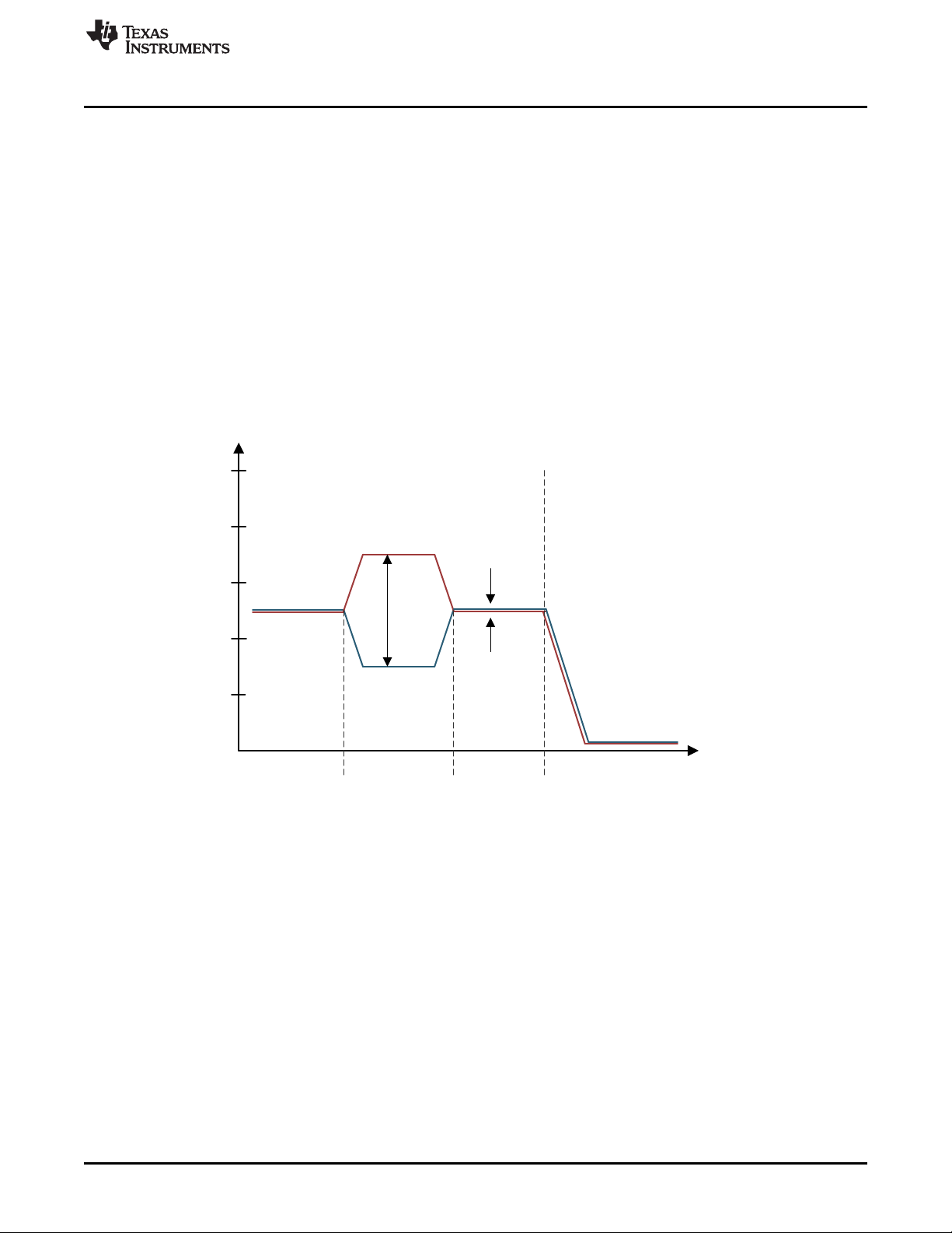
Recessive Dominant Recessive
Time, t
Typical Bus Voltage
Normal Mode
Standby Mode (Low
Power)
CANL
CANH
V
diff
V
diff
www.ti.com
In the recessive bus state, the bus is biased to a common mode of about 2.5 V via the high resistance
internal input resistors of the receiver of each node. Recessive is equivalent to logic high and is typically a
differential voltage on the bus of almost 0 V. The recessive state is also the idle state.
In the dominant bus state, the bus is driven differentially by one or more drivers. Current flows through the
termination resistors and generates a differential voltage on the bus. Dominant is equivalent to logic low
and is a differential voltage on the bus greater than the minimum threshold for a CAN dominant. A
dominant state overwrites the recessive state.
During arbitration, multiple CAN nodes may transmit a dominant bit at the same time. In this case the
differential voltage of the bus may be greater than the differential voltage of a single driver.
Transceivers with low power Standby Mode have a third bus state where the bus terminals are weakly
biased to ground via the high resistance internal resistors of the receiver. See Figure 1 and Figure 2.
Many of the pins can be configured for multiple purposes. Much of the parametric data is based on
internal links like the TXD/RXD_INT which represent the TXD and RXD of a standalone CAN transceiver.
The TCAN4550-Q1 has a test mode that maps these signals to an external pin in order to perform
compliance testing on the transceiver (TXD/RXD_INT_PHY) and CAN controller (TXD/RXD_INT_CAN)
independently.
Product Overview
Figure 1. CAN Bus States
SLLU312–July 2019
Submit Documentation Feedback
Copyright © 2019, Texas Instruments Incorporated
TCAN4550-Q1 Functional Safety-Manual
3
Page 4
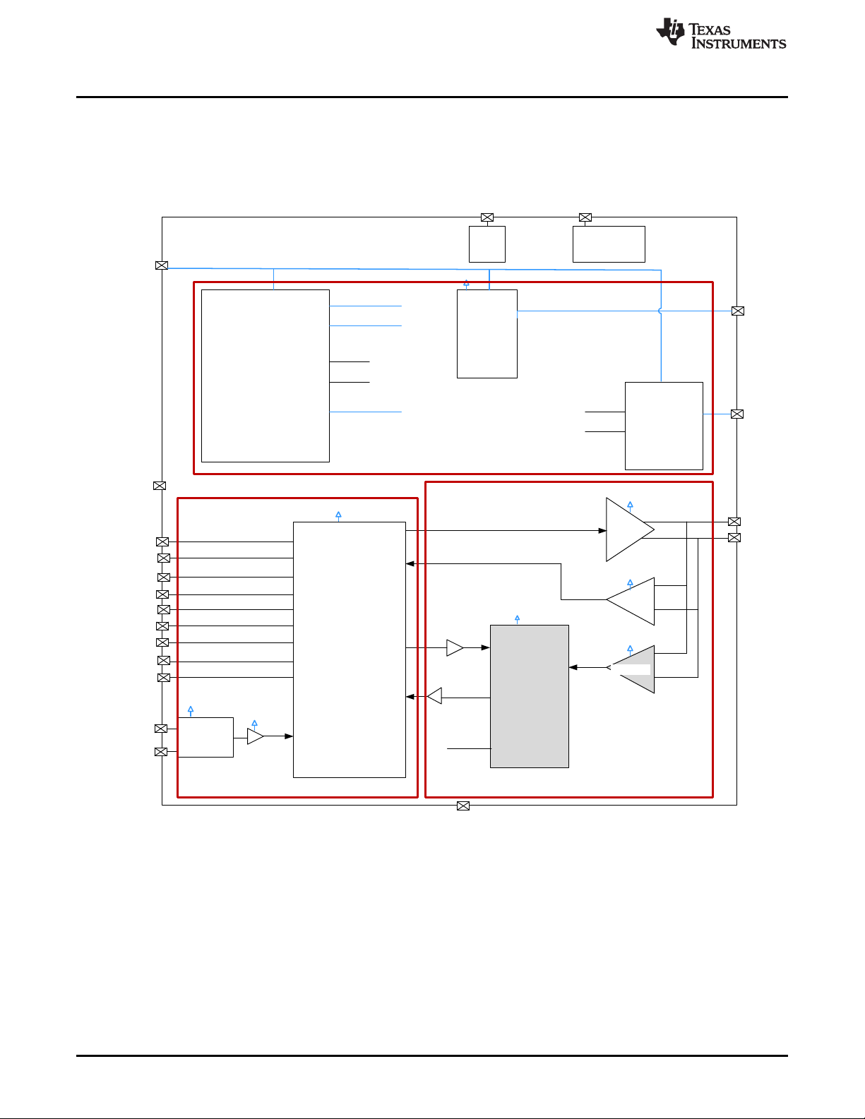
VSUP
VCCOUT
WAKEINH
RST
Crystal Osc
OSCIN
OSCOUT
INH
CTRL
CANH
CANL
RCVR
DRIVER
WUP RCVR
WUP/LUP
LOGIC
+ 32-Bit register
Comparator + analog
filter
WU
Clock from crystal osc/oscin
VCCOUT
Powerup
V3P6INT_SLEEP
V1P5INT_SLEEP
BG_1P25
ISRC_10U
V5INT
1.5V LDO
FLTR
WAKE
ISRC_10U
BG_1P25
V1P5INT
V1P5INT
V1P5INT_SLEEP
VCCOUT
VCCOUT
V3P6INT_SLEEP
VIO1
V1P5INT
WKRQ_nINT
CLKOUT/GPO1
SCLK
NCS
MOSI
MISO
NINT
Digital CORE
+
SRAM
GPO2
GND
VIO1
V5INT
Power and Control
CAN Transceiver and ControlSPI, M_CAN and Memory
Product Overview
3.1 Block Diagram
The TCAN4550-Q1 is a mixed signal device containing both analog and digital cores. The device
integrates the Bosch M_CAN revision 3.2.1.1 controller which is not covered in this document. Figure 2
and Figure 3 are the high level mixed signal and digital core functional block diagrams. CCLK is internally
connected to the crystal/CLKIN.
www.ti.com
4
Figure 2. TCAN4550-Q1 Mixed Signal Functional Block Diagram
TCAN4550-Q1 Functional Safety-Manual
Copyright © 2019, Texas Instruments Incorporated
Submit Documentation Feedback
SLLU312–July 2019
Page 5
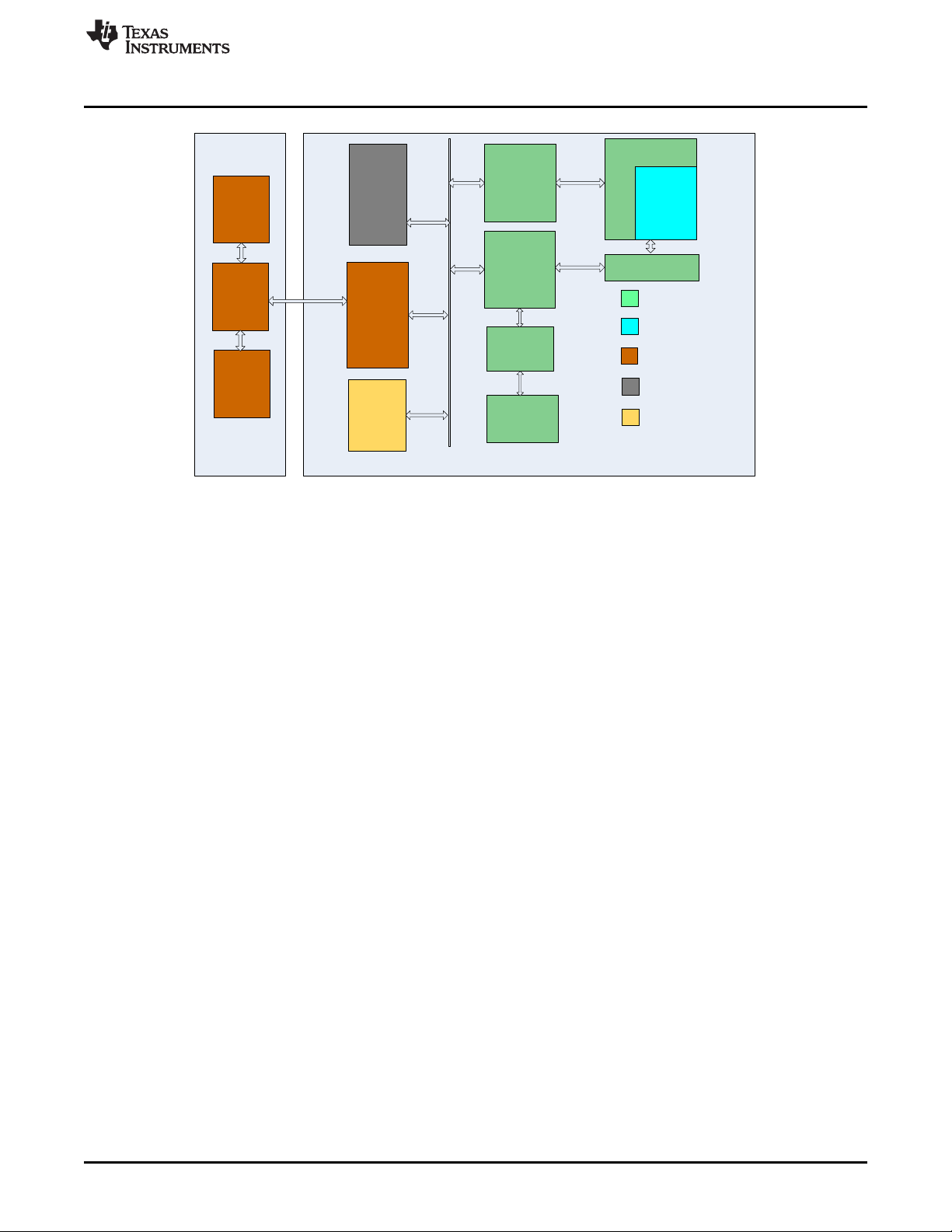
Main_core
mcan_core
supporting
blocks
(arbiter, time
stamp, driver
etc)
SPI
ECC
Controller
core
MCAN controller
Crystal
CCLK
Message
RAM
Watchdog
Register Map/
Interrupt
Logic
INH,
Device
Modes
FSM
Internal
Osc
SPI
High Power
(Standby/
Normal)
CAN
transceiver
logic, DTO
timer, bus
biasing
DFT
clock
WAKE
logic
Bus
biasing,
t
SILENT
timer
Sleep_core
DFT
www.ti.com
Product Overview
Figure 3. Digital Core Block Diagram and Clock Tree
3.2 Target Applications
The TCAN4550-Q1 is targeted at general-purpose automotive applications.
Examples of these types of applications include but are not limited to the applications that follow:
• General purpose applications where processor does not support CAN FD. See Figure 4
• CAN FD port expander
Figure 5 provides potential failure points that have diagnostic or test ability mechanisms. See Table 1 for
each potential failure point and subsection discussing this failure point.
SLLU312–July 2019
Submit Documentation Feedback
Copyright © 2019, Texas Instruments Incorporated
TCAN4550-Q1 Functional Safety-Manual
5
Page 6
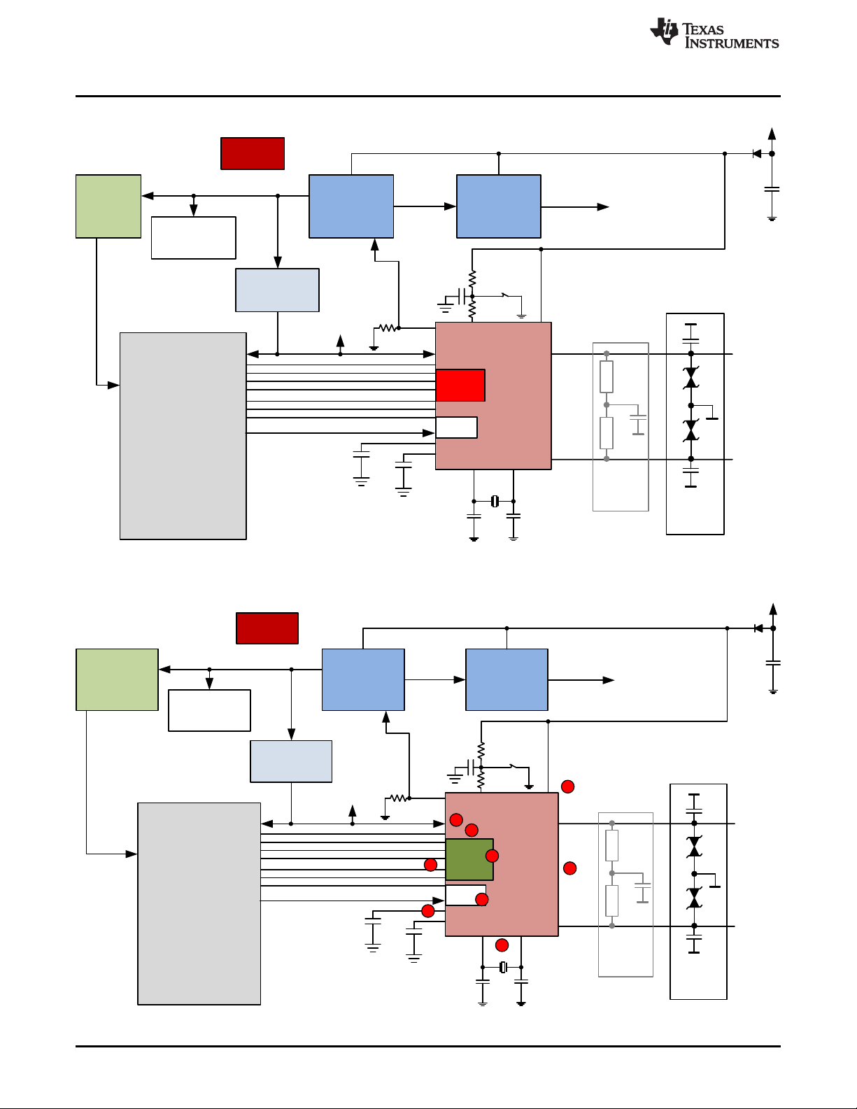
LM53635
Buck
3.3V, 3A
TPS57140
Buck
5V, 1.5A
TPS65917
PMIC
Processor
Without
CAN-FD Controller
Load SW
TPS22965
DDR3 Mem
TCAN4550
V
BAT
SPI
GPIO
3.3 V
12 V to 18 V
V
SUP
V
IO
INH
EN
EN
3.3 V
OSC1
WD
M_CAN
CAN-FD
Controller
Filters
100 NŸ
WAKE
33k
3.3 V
2-wire
CAN
bus
Optional:
Terminating
Node
Filtering,
Transient and
ESD
5 V
3k
CANH
CANL
10 µF
300 nF
GND
GND
22
nF
GND
V
CCOUT
FLTR
Add
Decoupling
Caps for All
Power
Connections
10
11
12
15
17
18
16
1
40 MHz
OSC2
20
1
4
3
2
5
6
RST
7
8
9
LM53635
Buck
3.3V, 3A
TPS57140
Buck
5V, 1.5A
TPS65917
PMIC
Processor
Without
CAN-FD Controller
Load SW
TPS22965
DDR3 Mem
TCAN4550RGY-Q1
V
BAT
SPI
GPIO
3.3 V
12 V to 18 V
V
SUP
V
IO
INH
EN
EN
3.3 V
Many V
OSC1
WD
CAN-FD
Controller
Filters
100 NŸ
WAKE
33k
3.3 V
2-wire
CAN
bus
Optional:
Terminating
Node
Filtering,
Transient and
ESD
5 V
3k
CANH
CANL
10 µF
300 nF
GND
GND
22
nF
GND
V
CCOUT
FLTR
Add
Decoupling
Caps for All
Power
Connections
10
11
12
15
17
18
16
1
40 MHz
OSC2
20
RST
Product Overview
www.ti.com
6
TCAN4550-Q1 Functional Safety-Manual
Figure 4. General Purpose Application
Figure 5. Potential Failure Points
Copyright © 2019, Texas Instruments Incorporated
Submit Documentation Feedback
SLLU312–July 2019
Page 7

www.ti.com
Table 1. Potential Failure Points and Section Figure 5
Potential
Failure
Point
from
Potential
Failure Point
Description
Section
Figure 5
Loss of clock
1
input
See Section 3.2.1.2 and Section 3.2.1.3
2 CAN bus See Section 3.2.1.3, Section 3.2.1.4, Section 3.2.1.5 and Section 3.2.1.6.5
3 Watchdog See Section 3.2.1.6.2
SPI/Processor
4
communication
5 Loss of V
6 Loss of V
See Section 3.2.1.6.1, Section 3.2.1.2, Section 3.2.1.3, Section 3.2.1.6.2, Section 3.2.1.6.3 and
Section 3.2.1.6.5
See Section 3.2.1.2, Section 3.2.1.3 and Section 3.2.1.6.5
SUP
See Section 3.2.1.2, Section 3.2.1.3 and Section 3.2.1.6.5
IO
7 RST pin failure See Section 3.2.1.6.3 and Section 3.2.1.6.4
M_CAN
8
Controller
9 Loss of V
See Section 3.2.1.5 and Section 3.2.1.6.5
See Section 3.2.1.3, Section 3.2.1.4 and Section 3.2.1.6.5
CCOUT
Table 2. Safety-Mechanisms
Product Overview
Safety-Mechanism
#
SM-01
SM-02 UV
SM-03 UV
SM-04 UV
Sleep Wake Error Timer
(SWE)t
Name Description Safety-Manual Section
Timer used for inactivity of expected functions.
INACTIVE
SUP
IO
CCOUT
Puts the device into Sleep mode
V
undervoltage detection and Interrupt
SUP
16'h0820[22]
VIOundervoltage detection and Interrupt
16'h820[21]
V
undervoltage detection and Interrupt
CCOUT
16'h0820[22]
SM-05 TSD Thermal Shutdown and Interrupt 16'h0820[19] 3.2.1.4
SM-06 IOS CAN bus short circuit current limiter 3.2.1.5
SM-07 SPI & M_CAN Test Mode Test Mode 3.2.1.5
SM-08
SM-09
SM-10
SPI & M_CAN Loop Back
Test Mode 1
SPI & M_CAN Loop Back
Test Mode 2
CAN Transceiver Test
Mode
Test Mode 3.2.1.5
Test Mode 3.2.1.5
Test Mode 3.2.1.5
Protocol Error in Data Phase; 16'h1050[28] points
SM-11 PED interrupt
to 16'h1044[10:8] DLEC[2:0]; Data Phase Last
Error Code
SM-12 PEA interrupt
SM-13 BEU interrupt
Protocol Error in Arbitration Phase; 16'h1050[27]
points to 16'h1044[2:0] LEC[2:0]; Last Error Code
Bit Error Uncorrected; 16'h1050[21] Message
RAM bit error detected, uncorrected
SM-14 Scratchpad write/read 3.2.1.6.1.1
SM-15 SPIERR flag SPI error detection and Interrupt 16'h0820[3] 3.2.1.6.1.2
SM-16
M_CAN forced dominant
and recessive
SM-17 SPI and FIFO TX and RX event FIFO 3.2.1.6.1.4
SM-18 ECC for Memory ECCERR detection and Interrupt 16'h0820[16] 3.2.1.6.1.5
SM-19 Timeout Watchdog WDTO detection and Interrupt 16'h0820[18] 3.2.1.6.2
SM-20 SCLK internal pull-up Floating pins 3.2.1.6.3
SM-21 SDI internal pull-up Floating pins 3.2.1.6.3
3.2.1.2
3.2.1.3
3.2.1.3
3.2.1.3
3.2.1.5 .1
3.2.1.5 .1
3.2.1.5 .1
3.2.1.6.1.3
SLLU312–July 2019
Submit Documentation Feedback
Copyright © 2019, Texas Instruments Incorporated
TCAN4550-Q1 Functional Safety-Manual
7
Page 8

Normal Mode
RST: L
INH: H
Wake Pin: Active
All GPIO: Active
SPI: Active
OSC: Active
V
CCOUT
: Enabled
Power On
Start Up
Standby Mode
RST: L
Wake Sources: CAN, WAKE
INH: H
Wake Pin: Active
All GPIO: Active
SPI: Active
OSC: Active
V
CCOUT
: Enabled
Sleep Mode
RST: L
Wake Sources: CAN, WAKE
INH: floating
Wake Pin: Active
nINT Pin: Off
nWKRQ Pin: Active
Other GPIO: Off
SPI: Off
OSC: Off
V
CCOUT
: Off
SPI Write
MO = 00
SPI Write
MO = 01
SPI Write
MO = 10
NOTE: Upon a wake event the device will
transition into Standby mode and must be
reconfigured using SPI
Wake-up Event:
CAN bus
or
WAKE Pin
SPI Write
MO = 00
RST Pin: Set high to
reset device. Once
finished set back low
UVLO V
SUP
TSD Protected
RST: L
Wake Sources: WAKE
INH: H
Wake Pin: Active
All GPIO: Active
SPI: Active
OSC: Active
V
CCOUT
: Off
Timer Start
Normal Mode
TSD = 1
TSD State
TSD Timer
TSD = 0 &
Timer Expires
TSD = 1 &
Timer Expires
UVIO Protected
RST: L
Wake Sources: CAN, WAKE
INH: H
Wake Pin: Active
All GPIO: Off
SPI: Off
OSC: Off
V
CCOUT
: On
Timer Start
UVIO State
UVIO Timer
UVIO = 1
UVIO = 1
Normal Mode
UVIO = 0
UVIO = 1 &
Timer Expires
TSD = 1
Resets Sleep
Core
Note:
x UVIO Protected status will lose the CLKIN/Crystal. During this time the digital core will reset and the M_CAN will have to be
reprogrammed. If timer times out and UVIO = 1 the device goes to sleep at which time all are cleared.
x If a Thermal Shutdown and UVIO event take place at the same time the device will enter sleep mode until the faults are rectified
Continued decrease below UV
SUP
;
the device will reset and clear
everything and come back on as if
a power up sequence has taken
place entering standby mode
Power Off
SWE timer
times out
Product Overview
Safety-Mechanism
#
SM-22 nCS internal pull-up Floating pins 3.2.1.6.3
SM-23 nWKRQ internal pull-up Floating pins 3.2.1.6.3
SM-24 RST internal pull-down Floating pins 3.2.1.6.3
SM-25 RST Pin System POR reset 3.2.1.6.4
3.2.1 Diagnostic Features
The TCAN4550-Q1 device has several features that determines specific fault conditions in a system and
indicate this back to the processor or place the device into a protected state that may include Sleep mode.
Figure 5 is used to indicate these fault conditions. Figure 6 provides the devices state diagram and shows
two protected modes and Sleep mode.
www.ti.com
Table 2. Safety-Mechanisms (continued)
Name Description Safety-Manual Section
8
TCAN4550-Q1 Functional Safety-Manual
Figure 6. State Diagram
Copyright © 2019, Texas Instruments Incorporated
SLLU312–July 2019
Submit Documentation Feedback
Page 9

www.ti.com
3.2.1.1 Mode Overview
The TCAN4550-Q1 has several operating modes: Normal, Standby and Sleep modes, as well as two
protected modes. The first three mode selections are made by the writing to SPI register. The two
protected modes are modified Standby modes used to protect the device or bus and are entered from
a fault condition only. The TCAN4550-Q1 automatically goes from Sleep to Standby mode when
receiving a WUP or LWU event. See Table 3 for the various modes and what parts of the device are
active during the each mode.
The TCAN4550-Q1 state diagram figure, see Figure 6, shows the biasing of the CAN bus in each of
the modes of operation.
RST
Mode
Normal L On On On On Off Off On On On On On On Saved
Standby L On On On On On On On On On On Off On Saved
TSD
ProtectedL On On On On On On On On On On Off Off Saved
UV
IO
ProtectedL Off On Off Off On On Off Off Off Off
Sleep L Off On Off Off On On Off Off Off Off Off Off Partially Saved
nINT nWKRQ INH GPO2
Pin
Table 3. Mode Overview
Low
Power
WAK
CAN
RX
WD SPI GPIO1 OSC CAN TX/ RX V
E Pin
Mode
Dependent
Product Overview
CCOUT
On Saved
Memory &
Configuration
3.2.1.2 Sleep Wake Error Timer (SWE)
The sleep wake error (SWE) timer is a four minute timer that is used to place the device into Sleep mode
due to certain faults. The SWE timer is used to help mitigate certain faults shown by items 1, 4, 5 and 6 in
Figure 5 and is considered safety mechanism SM-01.
The TCAN4550-Q1 fail-safe feature is used in order to reduce node power consumption in case of a
system issue. Fail-safe is the method the device uses to enter Sleep mode from various other modes
when specific issues arise. This feature uses the SWE timer to determine if the node processor can
communicate to the TCAN4550-Q1. The SWE timer is default enabled through the SWE_DIS; 16'h0800[1]
= 0 but can be disabled by writing a one to this bit. Even when the timer is disabled, the timer
automatically works for power up and power on resets. Fail-safe feature is default disabled but can be
enabled by writing a one to 16'h0800[13], FAIL-SAFE_EN.
Upon power up the SWE timer, t
INACTIVE
the TCAN4550-Q1, clear the PWRON flag or configure the device for Normal mode; see Figure 7. This
feature cannot be disabled. If the device has not had the PWRON flag cleared or been placed into Normal
mode, it enters Sleep mode. The device wakes up if the CAN bus provides a WUP or a local wake event
takes place, thus entering Standby mode. Once in Standby mode, t
t
INACTIVE
expires, the device re-enters Sleep mode.
The second failure mechanism that causes the device to use the fail-safe feature, if enabled, is when the
device receives a CANINT, CAN bus wake (WUP) or WAKE pin (LWU), while in Sleep mode such that the
device leaves Sleep mode and enters Standby mode. The processor has four minutes to clear the flags
and place the device into Normal mode. If this does not happen the device enters Sleep mode.
The third failure mechanism that can trigger the failsafe feature is a silent CAN bus. If the CANSLNT flag
persists for t
. Examples of events that could create this are the CLKIN or crystal stops working, the
INACTIVE
processor is no longer working and not able to exercise the SPI bus, a go-to-sleep command comes in
and the processor is not able to receive it or is not able to respond. See Figure 7.
, starts and the processor has typically four minutes to configure
SILENCE
and t
INACTIVE
timers starts. If
SLLU312–July 2019
Submit Documentation Feedback
Copyright © 2019, Texas Instruments Incorporated
TCAN4550-Q1 Functional Safety-Manual
9
Page 10

Standby Mode
SWE Timer
t
INACTIVE
Power On
Start Up
Sleep Mode
RST: L
Wake Sources: CAN, WAKE
INH: floating
Wake Pin: Active
nINT Pin: Off
nWKRQ Pin: Active
Other GPIO: Off
SPI: Off
OSC: Off
V
CCOUT
: Off
Stays in STBY mode
or switches to Normal
mode if programmed
No &
Cleared
Timed out
Does timer
Expire and PWRON
flag cleared?
SWE Timer
t
INACTIVE
Normal Mode
0800[13] = 1
Fail Safe Mode En
Bus Inactivity
t
SILENCE
timer
expires
setting CANSLNT
flag
Sleep Mode
RST: L
Wake Sources: CAN, WAKE
INH: floating
Wake Pin: Active
nINT Pin: Off
nWKRQ Pin: Active
Other GPIO: Off
SPI: Off
OSC: Off
V
CCOUT
: Off
Does timer
expire?
No &
Cleared
SWE Timer
t
INACTIVE
Monitoring CAN
Sleep Mode
RST: L
Wake Sources: CAN, WAKE
INH: floating
Wake Pin: Active
nINT Pin: Off
nWKRQ Pin: Active
Other GPIO: Off
SPI: Off
OSC: Off
V
CCOUT
: Off
Does timer
Expire and required
flags cleared?
Standby Mode
0800[13] = 1
Fail Safe Mode En
Bus Inactivity
Activity detected
leaving device in
current mode or
placing in selected
mode
Timed out
Power Up Failsafe Feature
Loss of Communication Failsafe Feature
Product Overview
www.ti.com
10
TCAN4550-Q1 Functional Safety-Manual
Figure 7. Fail-safe Feature State Diagram
Copyright © 2019, Texas Instruments Incorporated
Submit Documentation Feedback
SLLU312–July 2019
Page 11
www.ti.com
3.2.1.3 Undervoltage
The TCAN4550-Q1 has three undervoltage events that it monitors, UV
supply voltage to V
correct voltage levels. The V
this time. The device then disables the CAN transceiver and start putting the internal logic into a safe
state. If V
drops more, it eventually reaches the power on reset level. The device comes back up as if it
SUP
was the first time up once V
the device enters a UVIOprotected state. The digital I/O and the Crystal/CLKIN need VIOto perform
properly at the correct levels. These undervoltage levels help keep incorrect information off of the bus and
vice versa. These help mitigate faults shown as 1, 2, 4, 5, 6 and 9. The undervoltages are covered by
safety mechanism SM-02, SM-03 and SM-04.
drops below UV
SUP
CCOUT
SUP
, UVIOand UV
threshold the internal regulators may or may not provide the
SUP
SUP
CCOUT
LDO also provides 5 V for the CAN transceiver may enter UV
rises above the UV
threshold. When VIOdrops below the UVIOthreshold
SUP
Table 4. Under Voltage Lockout
Product Overview
. When the
at
CCOUT
V
> UV
> UV
< UV
> UV
< UV
SUP
SUP
SUP
SUP
SUP
SUP
V
> UV
> UV
> UV
< UV
< UV
IO
VIO
VIO
VIO
VIO
VIO
V
CCOUT
> UV
CCOUT
< UV
CCOUT
NA Protected High Impedance High (Recessive)
> UV
CCOUT
NA Protected High Impedance High Impedance
3.2.1.4 Thermal Shut Down
The TCAN4550-Q1 has a temperature monitor located by two components that can cause thermal issues;
V
LDO and CAN transceiver. This is a device protection mechanism. When TSD temperature is
CCOUT
reached, the device enters the TSD protected state as shown in Figure 6. In this state, the V
turned off and the CAN transceiver is disabled. This helps mitigate bus communication fault, shown as 2,
and V
issues, shown as 9, in Figure 5 and is considered safety mechanism SM-05. Undervoltage lock
CCOUT
out prevents operation of the device and communication with the MCU and the CAN FD Bus when there is
insufficient power on V
, VIOor V
SUP
3.2.1.5 CAN Bus Communication
CAN bus communication, shown as fault 2, is a main concern in a system. This can happen due to many
different mechanisms. Some have been covered in the previous sections of this document. The Bosch
M_CAN core has a CRC checker that validates the CAN data so corrupted data does not get transferred
to the node processor from the bus. The M_CAN core also provide two loop back test modes that allow
the implementer to determine if the data transmitted and received through the core are the same; see
Figure 8 loop back test mode 1 and 2. These three SPI↔M_CAN test modes are safety mechanism SM-
07, SM-08 and SM-09. If an error is detected there are two other test modes that can be utilized to
determine if the error is in the digital core or the transceiver; see Figure 8 and Figure 9. Driver and
receiver function test modes map the internal TXD_INT_PHY, RXD_INT_PHY and EN_INT signals to
GPIO to drive and receive data to CAN bus. Table 5 and Table 6 provide information on CAN bus state
when using transceiver test mode and is considered safety mechanism SM-10. Diagnostic tools like
dominant state timeout which makes sure the bus is not stuck dominant if the TXD_INT_PHY signal is
stuck low. The M_CAN signals TXD_INT_CAN and RXD_INT_CAN can be mapped to GPIO as an aid in
diagnostic to determine if the expected data is transmitted from SPI through M_CAN core and vise versa.
Table 5 and Table 6 provide information on CAN bus state when using transceiver test mode.
The TCAN4550-Q1 provides CAN bus short circuit current limiting and is considered safety mechanism
SM-06. These also mitigate potential faults 4 and 8.
DEVICE STATE BUS RXD_INT
Normal Per TXD_INT Mirrors Bus
Protected High Impedance High (Recessive)
Protected Recessive High Impedance
.
CCOUT
CCOUT
LDO is
DEVICE MODE TXD_INT INPUT
Normal
SLLU312–July 2019
Submit Documentation Feedback
Table 5. Driver Function Table
BUS OUTPUTS
CANH CANL
L H L Dominant
H or Open Z Z Biased Recessive
TCAN4550-Q1 Functional Safety-Manual
Copyright © 2019, Texas Instruments Incorporated
DRIVEN BUS STATE
11
Page 12

SCLK
CANH
V
CCINT2
CANL
SPI slave,
System
Controller
SDI
SDO
nCS
GPIO1
GPO2
M_CAN
Core
RX
TX
RXD_INT_CAN
TXD_INT_CAN
SCLK
CANH
V
CCINT2
CANL
SPI slave,
System
Controller
SDI
SDO
nCS
M_CAN
Core
RX
TX
= 1
SCLK
CANH
V
CCINT2
CANL
SPI slave,
System
Controller
SDI
SDO
nCS
M_CAN
Core
RX
TX
SPI & M_CAN Test Mode
SPI & M_CAN Loop Back Test Mode 1
SPI & M_CAN Loop Back Test Mode 2
Product Overview
DEVICE MODE TXD_INT INPUT
Table 5. Driver Function Table (continued)
BUS OUTPUTS
CANH CANL
Standby X Z Z Weak Pull to GND
Sleep X Z Z Weak Pull to GND
DRIVEN BUS STATE
Table 6. Receiver Function Table Normal and Standby Modes
www.ti.com
DEVICE MODE
CAN DIFFERENTIAL INPUTS
VID= V
CANH
– V
CANL
BUS STATE RXD_INT TERMINAL
VID≥ 0.9 V Dominant L
Normal
0.5 V < VID< 0.9 V Undefined Undefined
VID≤ 0.5 V Recessive H
VID≥ 1.15 V Dominant
Standby/Sleep
0.4 V < VID< 1.15 V Undefined
VID≤ 0.4 V Recessive
Any Open (VID≈ 0 V) Open H
See TCAN4550-Q1 data
sheet figure 24 for more
detial
12
TCAN4550-Q1 Functional Safety-Manual
Figure 8. SPI and M_CAN Test Modes
Copyright © 2019, Texas Instruments Incorporated
Submit Documentation Feedback
SLLU312–July 2019
Page 13

SCLK
CANH
V
CCINT2
CANL
SPI slave,
System
Controller
SDI
SDO
nCS
nINT
GPIO1
GPO2
M_CAN
Core
RX
TX
EN_INT
TXD_INT_PHY
RXD_INT_PHY
Transceiver Test Mode
www.ti.com
3.2.1.5.1 M_CAN
The M-CAN core which is an industry standard core supporting CAN FD and Classical CAN has three
interrupts that also lend themselves to confirmation the CAN bus information is accurate. These interrupts
are in register 16'h1050 and are as follows:
• 16'h1050[28] is an interrupt bit for Protocol Error in Data Phase (PED). If this bit shows up as a one
register 16'h1044[10:8] - DLEC (Data Phase Last Error Code) need to be reviewed to determine the
cause of the error. This is safety mechanism SM-11.
• 16'h1050[27] is an interrupt bit for Protocol Error in Arbitration Phase (PEA). If this bit shows up as a
one register 16'h1044[2:0] - LEC (Last Error Code) need to be reviewed to determine the cause of the
error. This is safety mechanism SM-12.
• 16'h1050[21] is an interrupt for Bit Error Uncorrected (BEU). This is an ECC between the M_CAN core
and message RAM. This is safety mechanism SM-13. This is not the same ECC error described in
processor communication section.
PED and PEA share the same code when the interrupt is set. These are three bit codes.
• 0 – No Error: No error occurred since LEC has been reset by successful reception or transmission
• 1 – Stuff Error: More than 5 equal bits in a sequence have occurred in a part of a received message
where this is not allowed
• 2 – Form Error: A fixed format part of a received frame has the wrong format
• 3 – AckError: The message transmitted by the M_CAN was not acknowledged by another node
• 4 – Bit1Error: During the transmission of a message (with the exception of the arbitration field), the
device wanted to send a recessive level (bit of logical value ‘1’), but the monitored bus value was
dominant
• 5 – Bit0Error: During the transmission of a message (or acknowledge bit, or active error flag, or
overload flag), the device wanted to send a dominant level (data or identifier bit logical value ‘0’), but
the monitored bus value was recessive. During Bus_Off recovery this status is set each time a
sequence of 11 recessive bits has been monitored. This enables the CPU to monitor the proceeding of
the Bus_Off recovery sequence (indicating the bus is not stuck at dominant or continuously disturbed)
• 6 – CRCError: The CRC check sum of a received message was incorrect. The CRC of an incoming
message does not match with the CRC calculated from the received data
• 7 – NoChange: Any read access to the Protocol Status Register re-initializes the LEC to ‘7’. When the
LEC shows the value ‘7’, no CAN bus event was detected since the last CPU read access to the
Protocol Status Register
Product Overview
Figure 9. CAN Transceiver Test Mode
SLLU312–July 2019
Submit Documentation Feedback
Copyright © 2019, Texas Instruments Incorporated
TCAN4550-Q1 Functional Safety-Manual
13
Page 14

Product Overview
3.2.1.6 Processor Communication
Communication between the node processor and the TCAN4550-Q1 contain several features that can
help determine if there is an issue and have a method for recovery. Several of the previous features like
the SWE timer and UVIOhelp with determining if communication with the processor is possible. Other
diagnostic tools that are available are timeout watchdog, floating terminals, device reset and several fault
interrupts available through SPI. Signal fail-safe in case of open (floating terminals) allows default state of
pin signals incase of an open terminal, see Table 8
3.2.1.6.1 SPI Integrity
The TCAN4550-Q1 does not support CRC for SPI communication. There are several ways to periodically
determine the SPI bus integrity is valid. These cover potential fault 4.
For the most robust and mostly continuous method is double transmit and reads and double reads to
determine if the data is the same. This method though robust reduces the bandwidth capabilities of the
device so performing several periodic test can be beneficial.
The periodic test that can be performed are as follows:
• Scratchpad write/read, safety mechanism SM-14
• SPIERR flag, safety mechanism SM-15
• M_CAN forced dominate and recessive testing, safety mechanism SM-16
• SPI and FIFO, safety mechanism SM-17
• ECC for memory, safety mechanism SM-18
www.ti.com
3.2.1.6.1.1 SPI Scratchpad
Using the TCAN4550-Q1 scratchpad by the processor makes it possible to write and read back data for
verification of accuracy. This verifies SPI interface to register space. It can also be accomplished without
interfering with CAN bus.
3.2.1.6.1.2 SPIERR
The TCAN4550-Q1 SPI controller checks all SPI transactions for transaction end on a byte boundary and
the length of the transaction is what was specified. The SPIERR flag sets if anything is incorrect, see
Table 9 for the various issues that sets the SPIERR interrupt.
3.2.1.6.1.3 M_CAN Forced Dominant and Recessive
The TCAN4550-Q1 M_CAN controller is used to force a dominant and recessive output by the processor.
The way to accomplish this without impacting the CAN bus is to use two of the SPI & M_CAN test modes
at the same time. Figure 8 shows the three SPI & M_CAN test modes. The top two are the ones to utilize
for this test. When used together the output goes to the GPO2 pin. This allows the processor to verify the
output is what is expected without needing to understand the CAN FD protocol. This is accomplished by
using register 16'h0800[21]; TEST_MODE_EN and 16'h0800[0]; TEST_MODE_CONFIG followed by
setting test register 16'1010 for M_CAN core. This shows SPI through M_CAN working.
3.2.1.6.1.4 SPI and FIFO
Another method for processor communication is accomplished by it using the Event FIFO for transmitting
and receiving. This is initiated by the processor and the TCAN4550-Q1 provides interrupts as described
as follows.
For transmitting, enabling the Tx Event FIFO option in the M_CAN requires SPI writes to the Tx Event
FIFO acknowledge register to manage the fill level. If these updates are not made, the Tx Event FIFO
eventually gives a Tx Event FIFO full (interrupt) and then the Tx Event FIFO Element Lost (interrupt).
For receiving, if the Rx messages are stored in Rx FIFO, then SPI writes are required to the Rx FIFO
Acknowledge register to manage the fill level. If this SPI access is not working, the Rx FIFO fills and gives
a Rx FIFO 0/1 Full (interrupt) and then Rx FIFO 0/1 Message Lost (interrupt).
These are runtime checks that indirectly ensure the SPI interface is working properly.
14
TCAN4550-Q1 Functional Safety-Manual
Copyright © 2019, Texas Instruments Incorporated
Submit Documentation Feedback
SLLU312–July 2019
Page 15

www.ti.com
3.2.1.6.1.5 ECC for Memory
The TCAN4550-Q1 provides single bit error correct when writing to and reading from MRAM with the
integrated ECC function.
For transmitting; when a message is to be transmitted, the data is read from internal MRAM. If during this
read (39 bits at a time for 4-bytes of data), a single bit is flipped, then this bit error is automatically
detected and corrected. If 2 bits are flipped, M_CAN exits and does not transmit any data. The device
drops into Standby Mode. The M_CAN Bit Error Uncorrected (BEU) interrupt is set. This is an
uncorrectable error case. There is no provision for 3+ bits being flipped, but statistically this is considered
highly improbable. (3+ error bits could alias into pass, 1, or 2 errors)
For receiving; when a received message is being read through SPI, the data is first fetched from MRAM. If
during this read (39 bits at a time), a single bit is flipped, it is corrected. If 2 bits are flipped, an ECCERR
interrupt is issued to inform the micro the read is corrupt. The ECCERR should be cleared and the read
tried again. There is no provision for 3+ bits flipped. This is the SPI to message RAM ECC error and not
be confused with the BEU interrupt in bus communication section.
3.2.1.6.2 Timeout Watchdog
The TCAN4550-Q1 contains a watchdog (WD) timeout function. When using the WD timeout function the
WD runs continuously. The WD is default enabled and can be configured with four different timer values.
WD is active in Normal and Standby modes and off in Sleep mode. Once the device enters Standby or
Normal mode the timer does not start until the first input trigger event. This event can be either writing a
one to register 16'h0800[18] or if selected, by changing the voltage level on the GPIO1 pin either high or
low when configured for watchdog input. If the first trigger is not set the watchdog is disabled. The first
trigger can happen in Standby mode or Normal mode. This is system implementation specific. While the
timer is running, a SPI command writing a one to 16'h0800[18] resets the WD_TIMER timer, or if
configured for pin control the GPIO1 behaves as the watchdog input bit.
The TCAN4550-Q1 has two ways of setting the trigger bit: via a SPI command and, if selected, through a
GPI (GPIO1 configured as GPI). When a GPI pin is used any rising or falling edge resets the timer. A
watchdog event can be conveyed back to the microprocessor in two methods: interrupt on nINT pin, or if
selected, the GPO2 pin can be programmed to toggle upon a WD timeout. A timeout can initiate one of
three actions by the TCAN4550-Q1: interrupt, INH toggle plus putting the device into Standby mode or
toggle watchdog output reset pin if enabled. The input CLKIN or crystal values needs to be entered into
reg 16'h0800[27] and is either 20 MHz or 40 MHz. See Table 7 for the register settings for the watchdog
function. This can help mitigate potential faults shown as 3 and 4 and is safety mechanism SM-19.
Product Overview
NOTE:
• If the device enters UVIOprotected mode, the watchdog timer is held in reset.
When the device returns to Standby mode, the timer resumes counting.
• Once the command to enter Sleep mode takes place, the WD timer is turned off
and does not trigger a watchdog event.
• If the any of the watchdog registers needs to be changed, the watchdog must
be disabled and the change made and then re-enabled.
SLLU312–July 2019
Submit Documentation Feedback
Copyright © 2019, Texas Instruments Incorporated
TCAN4550-Q1 Functional Safety-Manual
15
Page 16

Product Overview
Address BIT(S) Field Type Reset DESCRIPTION
16'h080
0
Table 7. Watchdog Registers and Descriptions
29:28 WD_TIMER R/W 2'b00
27 CLK_REF R/W 1'b1
23:22 GPO2_CONFIG R/W 2'b00
18 WD_BIT_SET W1C 1'b0
17:16 WD_ACTION R/W 2'b00
15:14 GPIO1_CONFIG RW 2'b01
3 WD_EN RXU 1'b1
www.ti.com
WD_TIMER: Watchdog timer
00 = 60 ms
01 = 600 ms
10 = 3 s
11 = 6 s
CLK_REF: CLKIN/Crystal frequency reference
0 = 20 MHz
1 = 40 MHz
GPO2_CONFIG: GPO2 configuration
00 = No action
01 = M_CAN_INT 0 interrupt (active low)
10 = Watchdog output
11 = Mirrors nINT pin
WD_BIT_SET: write a 1 to reset timer: if times out; this bit sets and
then the selected action from register 16'h0800[17:16] takes place.
Note: This is a self-clearing bit. Writing a 1 resets the timer and then
the bit clears.
WD_ACTION: Selected action when WD_TIMER times out
00 = Set interrupt flag and if a pin is configure to reflect WD output
as an interrupt the pin shows a low.
01 = Pulse INH pin and place device into Standby mode – high -
low - high ≈300 ms
10 = Pulse watchdog output pin if enabled – high - low - high ≈300
ms
11 = Reserved
Note: Interrupt flag is always set for a WD timeout event.
GPIO1_CONFIG: GPIO1 Pin Function Select
00 = GPO
01 = Reserved
10 = GPI – Automatically becomes a WD input trigger pin.
11 = Reserved
WD_EN - Watchdog Enable
0 = Disable
1 = Enabled
3.2.1.6.3 Floating Pins
In case of open (floating pins) default state of pin are provided by integrated pull-up or pull-down resistors
incase of an open pin. See Table 8 for details on pin bias conditions. These known states help keep
device pins at a defined level thus helping mitigate faults 4 and 7
Safety-
Mechanis
m #
SM-20 SCLK Pull up Weakly biases input
SM-21 SDI Pull up Weakly biases input
SM-22 nCS Pull up Weakly biases input so the device is not selected
SM-23 nWKRQ Pull up
SM-24 RST Pull down Weakly biases RST pin towards Normal operation mode
16
TCAN4550-Q1 Functional Safety-Manual
Table 8. Terminal Bias
Pin Pull-up or Pull-down COMMENT
Weakly biases output when using internal voltage rail. When using
open drain configuration an external pull up is needed.
Copyright © 2019, Texas Instruments Incorporated
Submit Documentation Feedback
SLLU312–July 2019
Page 17
V
SUP
14V
INH
V
IO
nWKRQ
14V
Device SPI
Access
Device ready to be
read and written to
Standby Mode
RST
Low
High
t
PULSE_WIDTH
•700 µs
Normal
or
Standby
Mode
www.ti.com
NOTE: The internal bias should not be relied upon as only termination, especially in noisy
environments but should be considered a fail-safe protection. Special care needs to be taken
when the device is used with MCUs utilizing open drain outputs.
3.2.1.6.4 RST Pin
The RST pin is a device reset pin. It has a weak internal pull down resistor for normal operation. If
communication has stopped with the TCAN4550-Q1 the RST pin can be pulsed high and then back low
for greater than t
settings and puts the device into Standby mode. If the device was in Normal or Standby mode, the INH
and nWKRQ pins remain active (on) and does not toggle; see Figure 10. If the device is in Sleep mode
and reset is toggled, the device enters Standby mode and at that time INH and nWKRQ turns on; see
Figure 11. This is considered SM-25.
After a RST has taken place a wait time of ≥ 700 µs should be used before reading or writing to the
TCAN4550-Q1
PULSE_WIDTH
Product Overview
to perform a power on reset to the device. This resets the device to the default
Figure 10. Timing for RST Pin in Normal and Standby Modes
SLLU312–July 2019
Submit Documentation Feedback
Copyright © 2019, Texas Instruments Incorporated
TCAN4550-Q1 Functional Safety-Manual
17
Page 18
V
SUP
14V
INH
V
IO
nWKRQ
Device SPI
Access
Device ready to be
read and written to
Standby Mode
RST
Float
High
t
PULSE_WIDTH
•700 µs
Sleep Mode
Low
14V
Low
•250 µs
Product Overview
Figure 11. Timing for RST Pin in Sleep Mode
3.2.1.6.5 Interrupt and Internal Fault Detection
The TCAN4550-Q1 provides error detection and status notification register and interrupts to notify the host
MCU of errors on internal transactions and SPI transactions, see Table 9. It also contains internal RAM
(FIFO Buffer) ECC protection. The internal RAM is protected by ECC for single bit correction due to
transient faults impacting RAM content during the read operation. See Table 10 and Table 11 for device
interrupts and M_CAN specific interrupts. The Bosch M_CAN core has many other interrupt and fault tools
that are provided in the data sheet.
www.ti.com
NOTE: Though these interrupts show certain failures the ones associated to safety mechanism have
been included in the document above.
Table 9. Internal SPI Status Field Descriptions (Address h000C)
Bit Field Type Reset Description
31:30 RSVD RO 1’b0 Reserved
29 Internal_read_error W1C 1’b0 Internal read received an error response
28 Internal_write_error W1C 1’b0 Internal write received an error response
27 Internal_error_log_write W1C 1’b0 Entry written to the Internal error log
26 Read_fifo_underflow W1C 1’b0 Read FIFO underflow after 1 or more read data words returned
25 Read_fifo_empty W1C 1’b0 Read FIFO empty for first read data word to return
24 Write_fifo_overflow W1C 1’b0 Write/command FIFO overflow
23:22 RSVD RO 1’b0 Reserved
21 SPI_end_error W1C 1’b0 SPI transfer did not end on a byte boundary
20 Invalid_command W1C 1’b0 Invalid SPI command received
19 Write_overflow W1C 1’b0 SPI write sequence had continue requests after the data transfer
18 write_underflow W1C 1’b0 SPI write sequence ended with less data transferred then
17 Read_overflow W1C 1’b0 SPI read sequence had continue requests after the data transfer
16 read_underflow W1C 1’b0 SPI read sequence ended with less data transferred then
was completed
requested
was completed
requested
18
TCAN4550-Q1 Functional Safety-Manual
Copyright © 2019, Texas Instruments Incorporated
Submit Documentation Feedback
SLLU312–July 2019
Page 19

www.ti.com
Product Overview
Table 9. Internal SPI Status Field Descriptions (Address h000C) (continued)
Bit Field Type Reset Description
15:8 RSVD RO 8’h00 Reserved
7:6 RSVD RO 1’b0 Reserved
5 Write_fifo_available RO 1’b0 write fifo empty entries is greater than or equal to the
4 Read_fifo_available RO 1’b0 Read fifo entries is greater than or equal to the
3 Internal_access_active RO U Internal Multiple transfer mode access in progress
2 Internal_error_interrupt RO 1’b0 Unmasked Internal error set
1 SPI_error_interrupt RO 1’b0 Unmasked SPI error set
0 Interrupt RO U Value of interrupt input level (active high)
write_fifo_threshold
read_fifo_threshold
Table 10. Interrupts Field Descriptions (Address h0820)
Bit Field Type Reset Description
31 CANBUSNOM RU 1'b0
30:24 RSVD R 7b'0000
000
23 SMS R/WC 1'b0 Sleep Mode Status (Flag & Not an interrupt) Only sets when
22 UVSUP R/WC 1'b0 Under Voltage V
21 UVIO R/WC 1'b0 Under Voltage V
20 PWRON R/WC/U 1'b1 Power ON
19 TSD R/WC 1'b0 Thermal Shutdown
18 WDTO RU/WC 1'b0 Watchdog Time Out
17 RSVD R 1'b0 Reserved
16 ECCERR R/WC 1'b0 Uncorrectable ECC error detected
15 CANINT R/WC 1'b0 Can Bus Wake Up Interrupt
14 LWU R/WC 1'b0 Local Wake Up
13 WKERR R/WC 1'b0 Wake Error
12 RSVD R 1'b0 Reserved
11 RSVD R 1'b0 Reserved
10 CANSLNT R/WC 1'b0 CAN Silent
9 RSVD R 1'b0 Reserved
8 CANDOM R/WC 1'b0 CAN Stuck Dominant
7 GLOBALERR R 1'b0 Global Error (Any Fault)
6 WKRQ R 1'b0 Wake Request
5 CANERR R 1'b0 CAN Error
4 RSVD R 1'b0 RSVD
3 SPIERR R 1'b0 SPI Error
2 RSVD R 1'b0 Reserved
1 M_CAN_INT R 1'b0 M_CAN global INT
0 VTWD R 1'b0 Global Voltage, Temp or WDTO
CAN Bus normal (Flag and Not Interrupt)
Changes to 1 when in Normal mode after first Dom to Rec
transition
Reserved
Sleep mode is entered by a WKERR, UVIO timeout, or
UVIO+TSD fault
and UV
SUP
IO
CCOUT
GLOBALERR: Logical OR of all faults in registers 0x0820-0824.
WKRQ: Logical OR of CANINT, LWU and WKERR.
CANBUSNOM is not an interrupt but a flag. In Normal mode after the first dominant-recessive transition, it
is set. It resets to 0 when entering Standby or Sleep modes or when a bus fault condition takes place in
Normal mode.
SLLU312–July 2019
Submit Documentation Feedback
Copyright © 2019, Texas Instruments Incorporated
TCAN4550-Q1 Functional Safety-Manual
19
Page 20

Product Overview
CANERR: Logical OR of CANSLNT and CANDOM faults.
SPIERR: is set if any of the SPI status register 16'h000C[30:16] is set.
• In the event of a SPI underflow, the error is not detected/alerted until the start of the next SPI
transaction.
• 16'h0010[30:16] are the mask for these errors
VTWD: Logical or of UV
, UVSUP, UVVIO, TSD, WDTO (Watchdog time out) and ECCERR.
CCOUT
CANINT: Indicates a WUP has occurred; Once a CANINT flag is set, LWU events are ignored. Flag can
be cleared by changing to Normal or Sleep modes.
LWU: Indicates a local wake event, from toggling the WAKE pin, has occurred. Once a LWU flag is set,
CANINT events is ignored. Flag can be cleared by changing to Normal or Sleep modes.
WKERR: If the device receives a wake up request WUP and does not transition to Normal mode or clear
the PWRON or Wake flag before t
, the device transitions to Sleep Mode. After the wake event, a
INACTIVE
Wake Error (WKERR) is reported and the SMS flag is set to 1.
NOTE: PWRON Flag is cleared by either writing a 1 or by going to Sleep mode or Normal mode
from Standby mode.
Table 11. MCAN Interrupts Field Descriptions (Address h0824)
Bit Field Type Reset Description
31:30 RSVD R 1'b0 Reserved
29 ARA R 1'b0 ARA: Access to Reserved Address
28 PED R 1'b0 PED: Protocol Error in Data Phase (Data Bit Time is used)
27 PEA R 1’b0 PEA: Protocol Error in Arbitration Phase (Nominal Bit Time is
26 WDI R 1'b0 WDI: Watchdog Interrupt
25 BO R 1'b0 BO: Bus_Off Status
24 EW R 1'b0 EW: Warning Status
23 EP R 1'b0 EP: Error Passive
22 ELO R 1'b0 ELO: Error Logging Overflow
21 BEU R 1'b0 BEU: Bit Error Uncorrected
20 BEC R 1'b0 BEC: Bit Error Corrected
19 DRX R 1’b0 DRX: Message stored to Dedicated Rx Buffer
18 TOO R 1'b0 TOO: Timeout Occurred
17 MRAF R 1'b0 MRAF: Message RAM Access Failure
16 TSW R 1'b0 TSW: Timestamp Wraparound
15 TEFL R 1'b0 TEFL: Tx Event FIFO Element Lost
14 TEFF R 1'b0 TEFF: Tx Event FIFO Full
13 TEFW R 1'b0 TEFW: Tx Event FIFO Watermark Reached
12 TEFN R 1'b0 TEFN: Tx Event FIFO New Entry
11 TFE R 1’b0 TFE: Tx FIFO Empty
10 TCF R 1'b0 TCF: Transmission Cancellation Finished
9 TC R 1'b0 TC: Transmission Completed
8 HPM R 1'b0 HPM: High Priority Message
7 RF1L R 1'b0 RF1L: Rx FIFO 1 Message Lost
6 RF1F R 1'b0 RF1F: Rx FIFO 1 Full
5 RF1W R 1'b0 RF1W: Rx FIFO 1 Watermark Reached
4 RF1N R 1'b0 RF1N: Rx FIFO 1 New Message
3 RF0L R 1’b0 RF0L: Rx FIFO 0 Message Lost
2 RF0F R 1'b0 RF0F: Rx FIFO 0 Full
used)
www.ti.com
20
TCAN4550-Q1 Functional Safety-Manual
Copyright © 2019, Texas Instruments Incorporated
Submit Documentation Feedback
SLLU312–July 2019
Page 21
Assess
Review
Plan
Review
Create
Review
Validate
Review
and Release
to Market
Periodic
Post-Release
Reviews
Phase 1:
Assess
Phase 2:
Plan
Phase 3:
Create
Phase 4:
Validate
Sustain
Identify New
Product
Opportunities
Develop
Project Plan
IC Design and
Layout
Develop
Product
Specification
IC Design
Verification
Manage Project Execution and Risks
Develop Test and Validation
Hardware (HW) and Software (SW)
Develop Data Sheet and other
Documentation
Product
Support
Product
Monitoring
IC Valdiation
IC Qualification
www.ti.com
Development Process for Management of Systematic Faults
Table 11. MCAN Interrupts Field Descriptions (Address h0824) (continued)
Bit Field Type Reset Description
1 RF0W R 1'b0 RF0W: Rx FIFO 0 Watermark Reached
0 RF0N R 1'b0 RF0N: Rx FIFO 0 New Message
4 Development Process for Management of Systematic Faults
4.1 TI New-Product Development Process
Texas Instruments has been developing mixed-signal automotive ICs for functional safety-critical and
nonsafety critical automotive applications for over fifteen years. Automotive markets have strong
requirements regarding quality management and product reliability. Though not explicitly developed for
compliance to a functional safety standard, the TI new-product development process already featured
many elements necessary to manage systematic faults.
The device was developed using TI’s new product development process which has been certified as
compliant to ISO 9001 / IATF 16949 as assessed by Det Norske Veritas Certification, Inc.
The standard development process breaks development into phases:
• Assess
• Plan
• Create
• Validate
Figure 12 shows the standard process.
SLLU312–July 2019
Submit Documentation Feedback
Figure 12. TI New-Product Development Process
Copyright © 2019, Texas Instruments Incorporated
TCAN4550-Q1 Functional Safety-Manual
21
Page 22

IMPORTANT NOTICE AND DISCLAIMER
TI PROVIDES TECHNICAL AND RELIABILITY DATA (INCLUDING DATASHEETS), DESIGN RESOURCES (INCLUDING REFERENCE
DESIGNS), APPLICATION OR OTHER DESIGN ADVICE, WEB TOOLS, SAFETY INFORMATION, AND OTHER RESOURCES “AS IS”
AND WITH ALL FAULTS, AND DISCLAIMS ALL WARRANTIES, EXPRESS AND IMPLIED, INCLUDING WITHOUT LIMITATION ANY
IMPLIED WARRANTIES OF MERCHANTABILITY, FITNESS FOR A PARTICULAR PURPOSE OR NON-INFRINGEMENT OF THIRD
PARTY INTELLECTUAL PROPERTY RIGHTS.
These resources are intended for skilled developers designing with TI products. You are solely responsible for (1) selecting the appropriate
TI products for your application, (2) designing, validating and testing your application, and (3) ensuring your application meets applicable
standards, and any other safety, security, or other requirements. These resources are subject to change without notice. TI grants you
permission to use these resources only for development of an application that uses the TI products described in the resource. Other
reproduction and display of these resources is prohibited. No license is granted to any other TI intellectual property right or to any third
party intellectual property right. TI disclaims responsibility for, and you will fully indemnify TI and its representatives against, any claims,
damages, costs, losses, and liabilities arising out of your use of these resources.
TI’s products are provided subject to TI’s Terms of Sale (www.ti.com/legal/termsofsale.html) or other applicable terms available either on
ti.com or provided in conjunction with such TI products. TI’s provision of these resources does not expand or otherwise alter TI’s applicable
warranties or warranty disclaimers for TI products.
Mailing Address: Texas Instruments, Post Office Box 655303, Dallas, Texas 75265
Copyright © 2020, Texas Instruments Incorporated
 Loading...