

Texas Instruments SN74LVC1G66DBV, SN74LVC1G66DCK, SN74LVC1G66DRL, SN74LVC1G66DRY, SN74LVC1G66DSF Schematic [ru]
...
3
2
4
51
A V
CC
C
B
GND
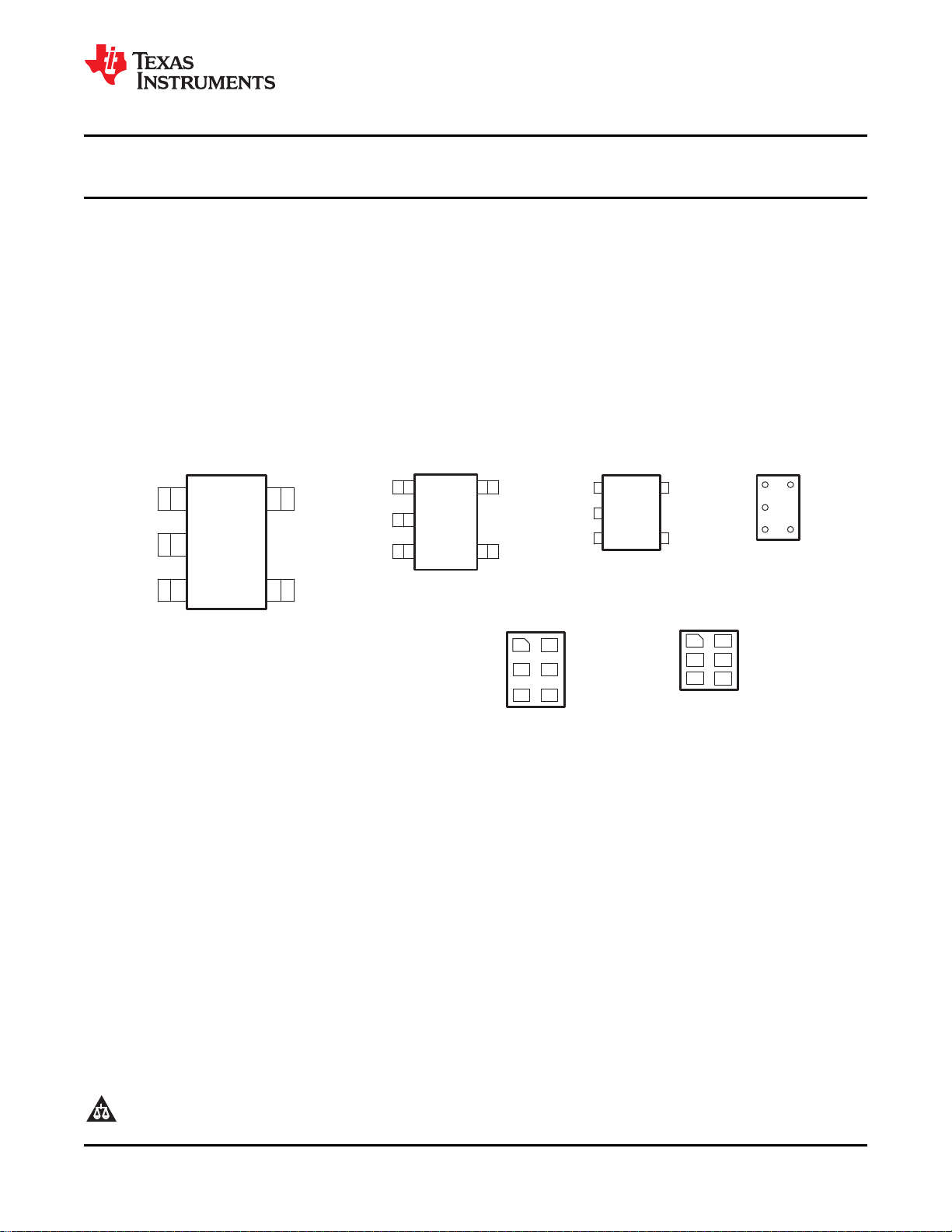
DBV PACKAGE
(TOP VIEW)
YZP PACKAGE
(BOTTOM VIEW)
DCK PACKAGE
(TOP VIEW)
3
2
4
51
A V
CC
C
B
GND
3
2
4
51
A V
CC
C
B
GND
A
GND
V
CC
C
B
DRL PACKAGE
(TOP VIEW)
See mechanical drawings for dimensions.
1
423
5
DRY PACKAGE
(TOP VIEW)
B NC
A
6
5
4
2
3
GND
C
V
CC
1
A
GND
DSF PACKAGE
(TOP VIEW)
B
V
CC
C
NC
6
5
4
2
3
1
SN74LVC1G66
www.ti.com
SCES323N –JUNE 2001–REVISED NOVEMBER 2012
SINGLE BILATERAL ANALOG SWITCH
Check for Samples: SN74LVC1G66
1
FEATURES
2
• Available in the Texas Instruments NanoFree™
Package (VCC= 4.5 V)
• 1.65-V to 5.5-V VCCOperation • Latch-Up Performance Exceeds 100 mA Per
• Inputs Accept Voltages to 5.5 V
• Max tpdof 0.8 ns at 3.3 V
• High On-Off Output Voltage Ratio
• High Degree of Linearity
• High Speed, Typically 0.5 ns
(VCC= 3 V, CL= 50 pF)
• Low On-State Resistance, Typically ≉≉5.5 Ω
JESD 78, Class II
• ESD Protection Exceeds JESD 22
– 2000-V Human-Body Model (A114-A)
– 200-V Machine Model (A115-A)
– 1000-V Charged-Device Model (C101)
DESCRIPTION/ORDERING INFORMATION
This single analog switch is designed for 1.65-V to 5.5-V VCCoperation.
The SN74LVC1G66 can handle both analog and digital signals. The device permits signals with amplitudes of up
to 5.5 V (peak) to be transmitted in either direction.
NanoFree™ package technology is a major breakthrough in IC packaging concepts, using the die as the
package.
Applications include signal gating, chopping, modulation or demodulation (modem), and signal multiplexing for
analog-to-digital and digital-to-analog conversion systems.
1
2NanoFree is a trademark of Texas Instruments.
PRODUCTION DATA information is current as of publication date.
Products conform to specifications per the terms of the Texas
Instruments standard warranty. Production processing does not
necessarily include testing of all parameters.
Please be aware that an important notice concerning availability, standard warranty, and use in critical applications of
Texas Instruments semiconductor products and disclaimers thereto appears at the end of this data sheet.
Copyright © 2001–2012, Texas Instruments Incorporated
B
C
A
1
4
2
SN74LVC1G66
SCES323N –JUNE 2001–REVISED NOVEMBER 2012
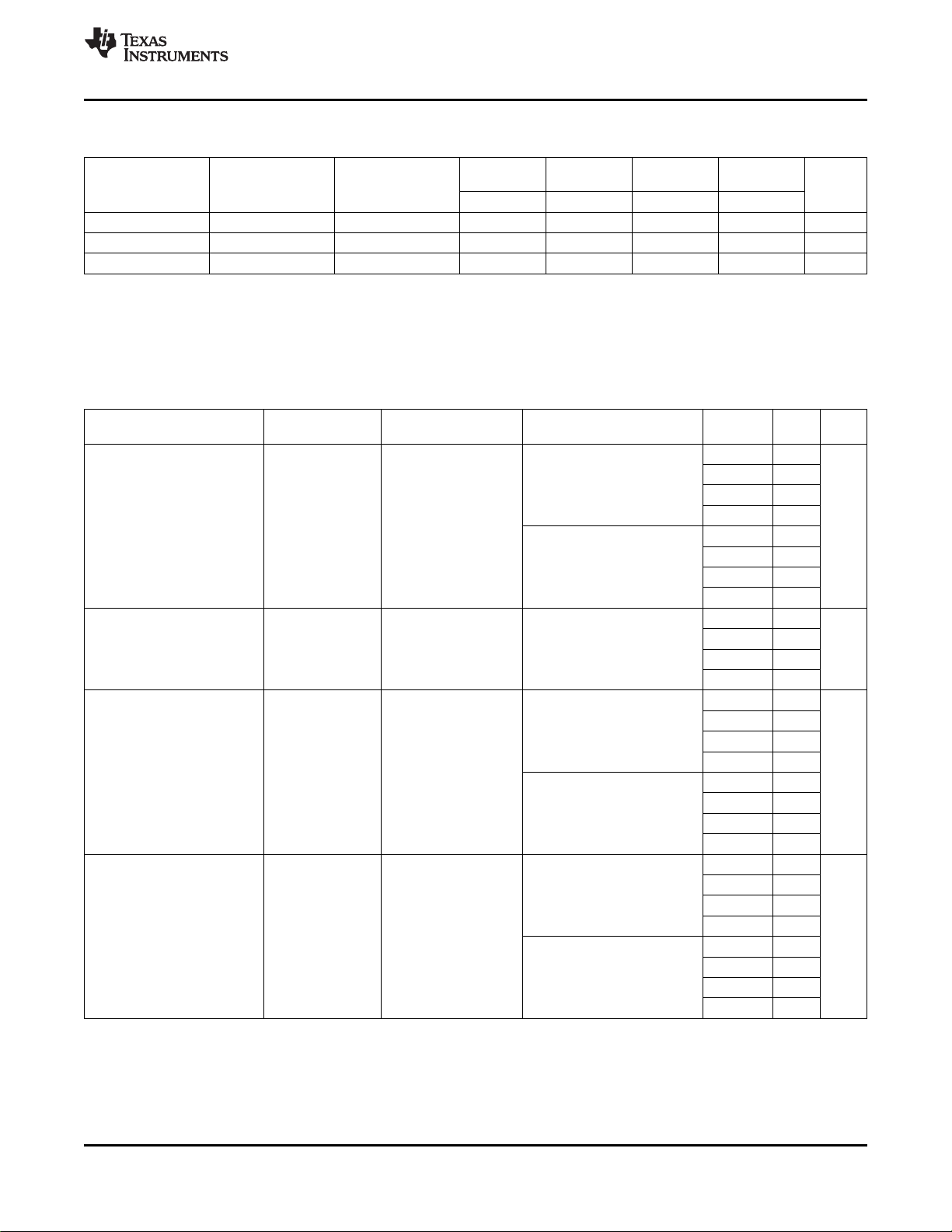
Table 1. ORDERING INFORMATION
T
A
NanoFree™ – WCSP (DSBGA)
0.23-mm Large Bump – YZP (Pb- Reel of 3000 SN74LVC1G66YZPR _ _ _C6_
free)
SOT (SOT-23) – DBV C66_
–40°C to 85°C
(1) Package drawings, standard packing quantities, thermal data, symbolization, and PCB design guidelines are available at
www.ti.com/sc/package.
(2) DBV/DCK: The actual top-side marking has one additional character that designates the assembly/test site.
YZP: The actual top-side marking has three preceding characters to denote year, month, and sequence code, and one following
character to designate the assembly/test site. Pin 1 identifier indicates solder-bump composition (1 = SnPb, • = Pb-free).
SOT (SC-70) – DCK
SOT (SOT-553) – DRL Reel of 4000 SN74LVC1G66DRLR
QFN – DRY Reel of 5000 SN74LVC1G66DRYR
µQFN – DSF Reel of 5000 SN74LVC1G66DSFR
PACKAGE
(1)
Reel of 3000 SN74LVC1G66DBVR
Reel of 250 SN74LVC1G66DBVT
Reel of 3000 SN74LVC1G66DCKR
Reel of 250 SN74LVC1G66DCKT
Jumbo Reel of
10000
ORDERABLE PART NUMBER TOP-SIDE MARKING
SN74LVC1G66DCKJ
C6_
C6
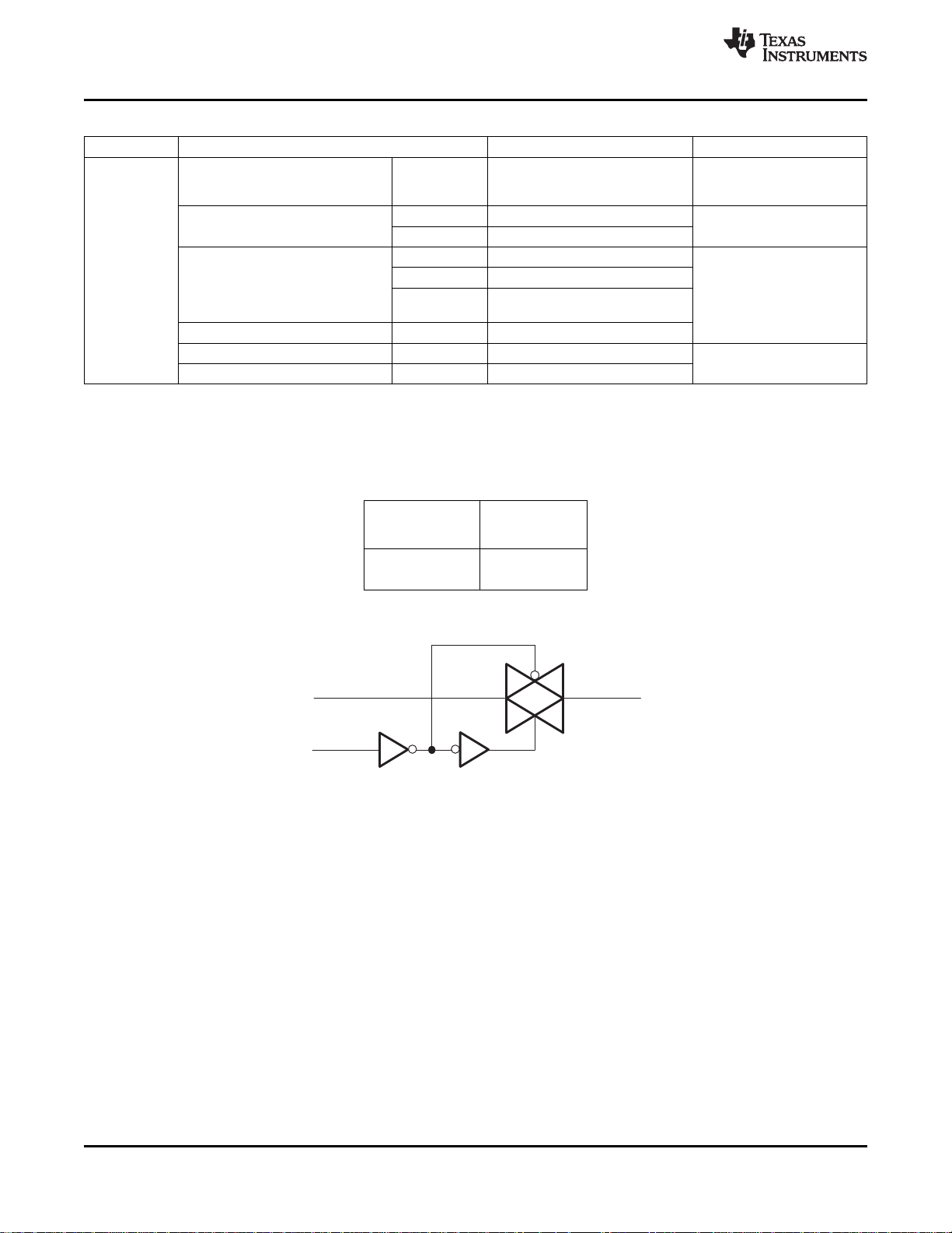
FUNCTION TABLE
CONTROL
INPUT SWITCH
(C)
L OFF
H ON
www.ti.com
(2)
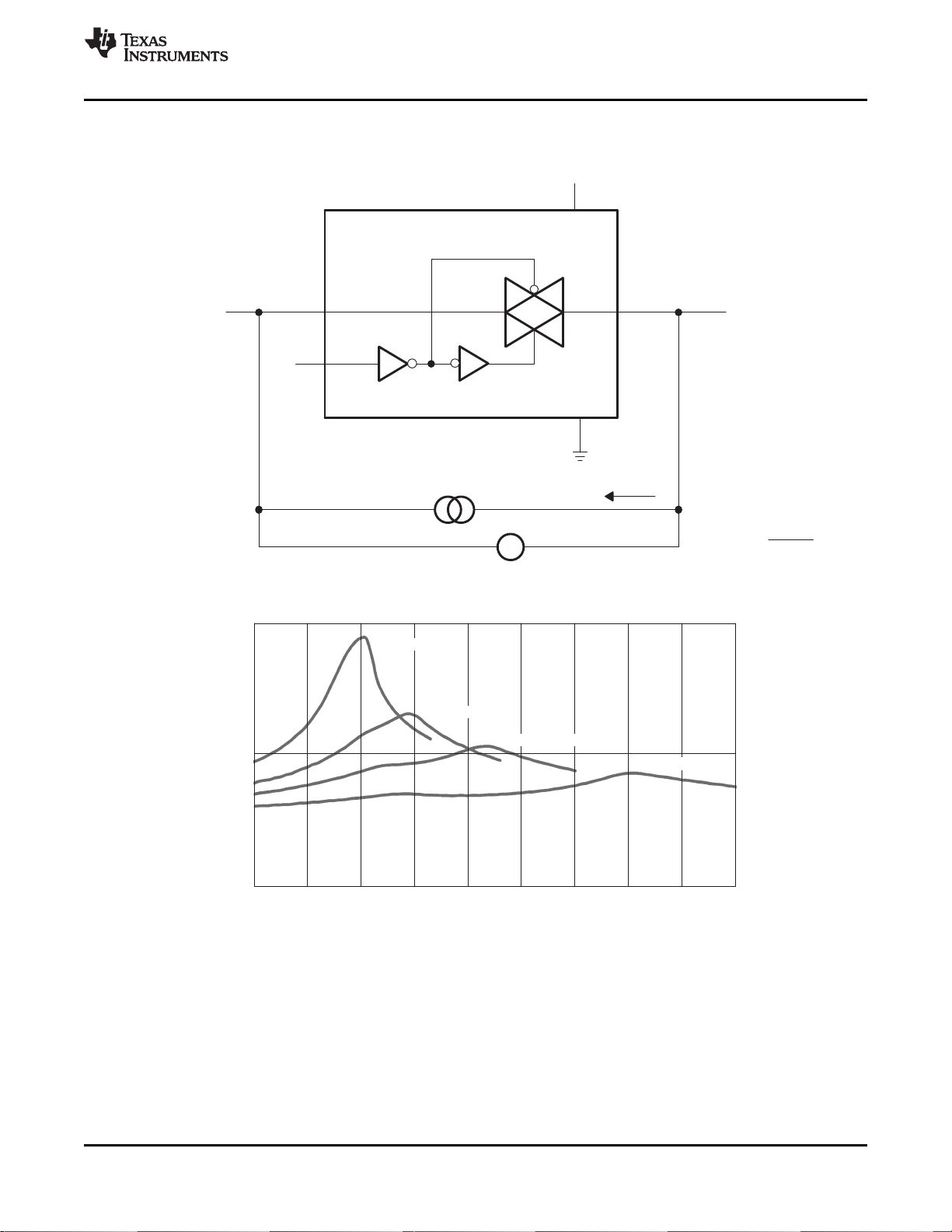
LOGIC DIAGRAM (POSITIVE LOGIC)
2 Submit Documentation Feedback Copyright © 2001–2012, Texas Instruments Incorporated
Product Folder Links: SN74LVC1G66
SN74LVC1G66
www.ti.com
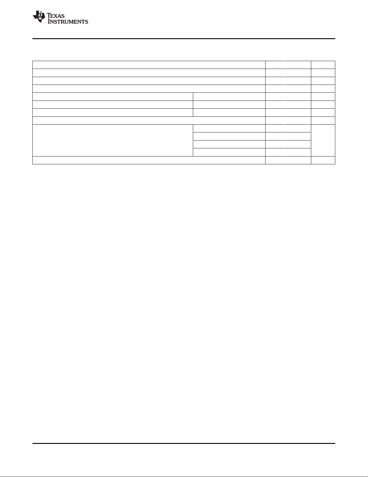
Absolute Maximum Ratings
(1)
SCES323N –JUNE 2001–REVISED NOVEMBER 2012
over operating free-air temperature range (unless otherwise noted)
MIN MAX UNIT
V
V
V
I
I
I
Supply voltage range
CC
Input voltage range
I
Switch I/O voltage range
I/O
Control input clamp current VI< 0 –50 mA
IK
I/O port diode current V
IOK
On-state switch current V
T
Continuous current through VCCor GND ±100 mA
θ
T
Package thermal impedance
JA
Storage temperature range –65 150 °C
stg
(1) Stresses beyond those listed under "absolute maximum ratings" may cause permanent damage to the device. These are stress ratings
only, and functional operation of the device at these or any other conditions beyond those indicated under "recommended operating
conditions" is not implied. Exposure to absolute-maximum-rated conditions for extended periods may affect device reliability.
(2) All voltages are with respect to ground, unless otherwise specified.
(3) The input and output negative-voltage ratings may be exceeded if the input and output clamp-current ratings are observed.
(4) This value is limited to 5.5 V maximum.
(5) The package thermal impedance is calculated in accordance with JESD 51-7.
(2)
(2) (3)
(2) (3) (4)
(5)
–0.5 6.5 V
–0.5 6.5 V
–0.5 VCC+ 0.5 V
I/O
I/O
< 0 or V
< 0 to V
CC
I/O
> V
CC
±50 mA
±50 mA
DBV package 206
DCK package 252
DRL package 142
YZP package 132
°C/W
Copyright © 2001–2012, Texas Instruments Incorporated Submit Documentation Feedback 3
Product Folder Links: SN74LVC1G66
SN74LVC1G66
SCES323N –JUNE 2001–REVISED NOVEMBER 2012
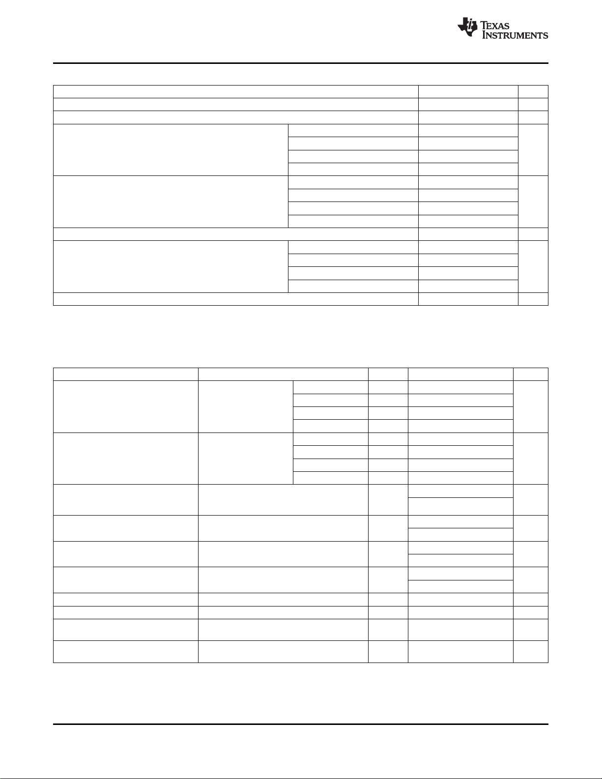
Recommended Operating Conditions
(1)
www.ti.com
MIN MAX UNIT
V
V
Supply voltage 1.65 5.5 V
CC
I/O port voltage 0 V
I/O
CC
VCC= 1.65 V to 1.95 V VCC× 0.65
V
High-level input voltage, control input V
IH
VCC= 2.3 V to 2.7 V VCC× 0.7
VCC= 3 V to 3.6 V VCC× 0.7
VCC= 4.5 V to 5.5 V VCC× 0.7
VCC= 1.65 V to 1.95 V VCC× 0.35
V
Low-level input voltage, control input V
IL
VCC= 2.3 V to 2.7 V VCC× 0.3
VCC= 3 V to 3.6 V VCC× 0.3
VCC= 4.5 V to 5.5 V VCC× 0.3
V
Control input voltage 0 5.5 V
I
VCC= 1.65 V to 1.95 V 20
Δt/Δv Input transition rise/fall time ns/V
VCC= 2.3 V to 2.7 V 20
VCC= 3 V to 3.6 V 10
VCC= 4.5 V to 5.5 V 10
T
Operating free-air temperature –40 85 °C
A
(1) All unused inputs of the device must be held at VCCor GND to ensure proper device operation. Refer to the TI application report,
Implications of Slow or Floating CMOS Inputs, literature number SCBA004.
V
Electrical Characteristics
over recommended operating free-air temperature range (unless otherwise noted)
PARAMETER TEST CONDITIONS V
IS= 4 mA 1.65 V 12 30
IS= 8 mA 2.3 V 9 20
IS= 24 mA 3 V 7.5 15
IS= 32 mA 4.5 V 5.5 10
IS= 4 mA 1.65 V 74.5 120
IS= 8 mA 2.3 V 20 30
IS= 24 mA 3 V 11.5 20
IS= 32 mA 4.5 V 7.5 15
r
r
I
I
I
I
ΔI
C
C
C
On-state switch resistance Ω
on
Peak on resistance Ω
on(p)
Off-state switch leakage
S(off)
current
On-state switch leakage VI= VCCor GND, VC= VIH, VO= Open
S(on)
current (see Figure 4)
Control input current VC= VCCor GND 5.5 V μA
I
Supply current VC= VCCor GND 5.5 V μA
CC
Supply current change VC= VCC– 0.6 V 5.5 V 500 μA
CC
Control input capacitance 5 V 2 pF
ic
Switch input/output
io(off)
capacitance
Switch input/output 5 V
io(on)
capacitance
(1) TA= 25°C
VI= VCCor GND,
VC= V
IH
(see Figure 1 and
Figure 2)
VI= VCCor GND,
VC= V
IH
(see Figure 1 and
Figure 2)
VI= VCCand VO= GND or ±1
VI= GND and VO= VCC, 5.5 V μA
VC= VIL(see Figure 3)
CC
MIN TYP
5.5 V μA
(1)
MAX UNIT
(1)
±0.1
±1
(1)
±0.1
±1
(1)
±0.1
10
(1)
1
5 V 6 pF
13 pF
4 Submit Documentation Feedback Copyright © 2001–2012, Texas Instruments Incorporated
Product Folder Links: SN74LVC1G66
SN74LVC1G66
www.ti.com
SCES323N –JUNE 2001–REVISED NOVEMBER 2012
Switching Characteristics
over recommended operating free-air temperature range (unless otherwise noted) (see Figure 5)
PARAMETER UNIT
(1)
t
pd
(2)
t
en
(3)
t
dis
(1) t
(2) t
(3) t
and t
PLH
switch and the specified load capacitance, when driven by an ideal voltage source (zero output impedance).
and t
PZL
and t
PLZ
are the same as tpd. The propagation delay is the calculated RC time constant of the typical on-state resistance of the
PHL
are the same as ten.
PZH
are the same as t
PHZ
FROM TO
(INPUT) (OUTPUT)
A or B B or A 2 1.2 0.8 0.6 ns
C A or B 2.5 12 1.9 6.5 1.8 5 1.5 4.2 ns
C A or B 2.2 10 1.4 6.9 2 6.5 1.4 5 ns
.
dis
VCC= 1.8 V VCC= 2.5 V VCC= 3.3 V VCC= 5 V
± 0.15 V ± 0.2 V ± 0.3 V ± 0.5 V
MIN MAX MIN MAX MIN MAX MIN MAX
Analog Switch Characteristics
TA= 25°C
PARAMETER V
Frequency response
(1)
(switch ON)
Crosstalk
(control input to signal output)
Feedthrough attenuation
(2)
(switch OFF)
Sine-wave distortion A or B B or A %
(1) Adjust finvoltage to obtain 0 dBm at output. Increase finfrequency until dB meter reads –3 dB.
(2) Adjust finvoltage to obtain 0 dBm at input.
FROM TO TEST
(INPUT) (OUTPUT) CONDITIONS
CC
TYP UNIT
1.65 V 35
CL= 50 pF, RL= 600 Ω,
fin= sine wave
(see Figure 6)
A or B B or A MHz
CL= 5 pF, RL= 50 Ω,
fin= sine wave
(see Figure 6)
2.3 V 120
3 V 175
4.5 V 195
1.65 V >300
2.3 V >300
3 V >300
4.5 V >300
1.65 V 35
C A or B fin= 1 MHz (square wave) mV
CL= 50 pF, RL= 600 Ω,
(see Figure 7)
2.3 V 50
3 V 70
4.5 V 100
1.65 V –58
CL= 50 pF, RL= 600 Ω,
fin= 1 MHz (sine wave)
(see Figure 8)
A or B B or A dB
CL= 5 pF, RL= 50 Ω,
fin= 1 MHz (sine wave)
(see Figure 8)
2.3 V –58
3 V –58
4.5 V –58
1.65 V –42
2.3 V –42
3 V –42
4.5 V –42
1.65 V 0.1
CL= 50 pF, RL= 10 kΩ,
fin= 1 kHz (sine wave)
(see Figure 9)
2.3 V 0.025
3 V 0.015
4.5 V 0.01
1.65 V 0.15
CL= 50 pF, RL= 10 kΩ,
fin= 10 kHz (sine wave)
(see Figure 9)
2.3 V 0.025
3 V 0.015
4.5 V 0.01
Copyright © 2001–2012, Texas Instruments Incorporated Submit Documentation Feedback 5
Product Folder Links: SN74LVC1G66
SN74LVC1G66
SCES323N –JUNE 2001–REVISED NOVEMBER 2012
www.ti.com
Operating Characteristics
TA= 25°C
PARAMETER UNIT
CpdPower dissipation capacitance f = 10 MHz 8 9 9 11 pF
TEST
CONDITIONS
VCC= 1.8 V VCC= 2.5 V VCC= 3.3 V VCC= 5 V
TYP TYP TYP TYP
6 Submit Documentation Feedback Copyright © 2001–2012, Texas Instruments Incorporated
Product Folder Links: SN74LVC1G66
100
10
1
0.0 0.5 1.0 1.5 2.0 2.5 3.0 3.5 4.0 4.5
VCC = 1.65 V
VCC = 2.3 V
VCC = 3.0 V
VCC = 4.5 V
VIN − V
r
on
− Ω
V
CC
VI = V
CC
or GND
V
O
r
on
+
VI* V
O
I
S
W
V
I
− V
O
GND(ON)
V
B or A
C
A or B
V
CC
V
IH
V
C
I
S
SN74LVC1G66
www.ti.com
SCES323N –JUNE 2001–REVISED NOVEMBER 2012
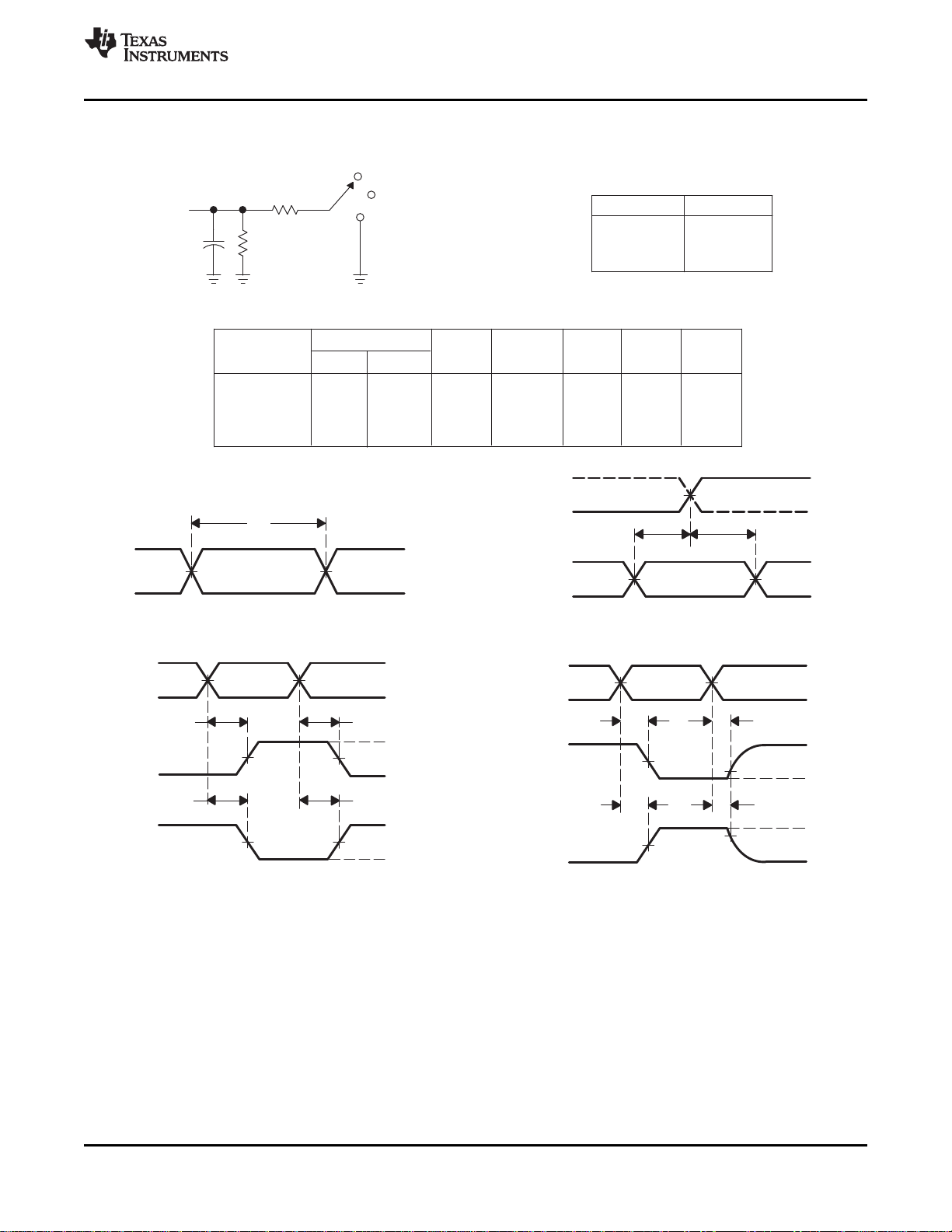
PARAMETER MEASUREMENT INFORMATION
Figure 1. On-State Resistance Test Circuit
Figure 2. Typical ronas a Function of Input Voltage (VI) for VI= 0 to V
CC
Copyright © 2001–2012, Texas Instruments Incorporated Submit Documentation Feedback 7
Product Folder Links: SN74LVC1G66
V
CC
V
O
GND(ON)
B or A
C
A or B
V
CC
V
IH
V
C
A
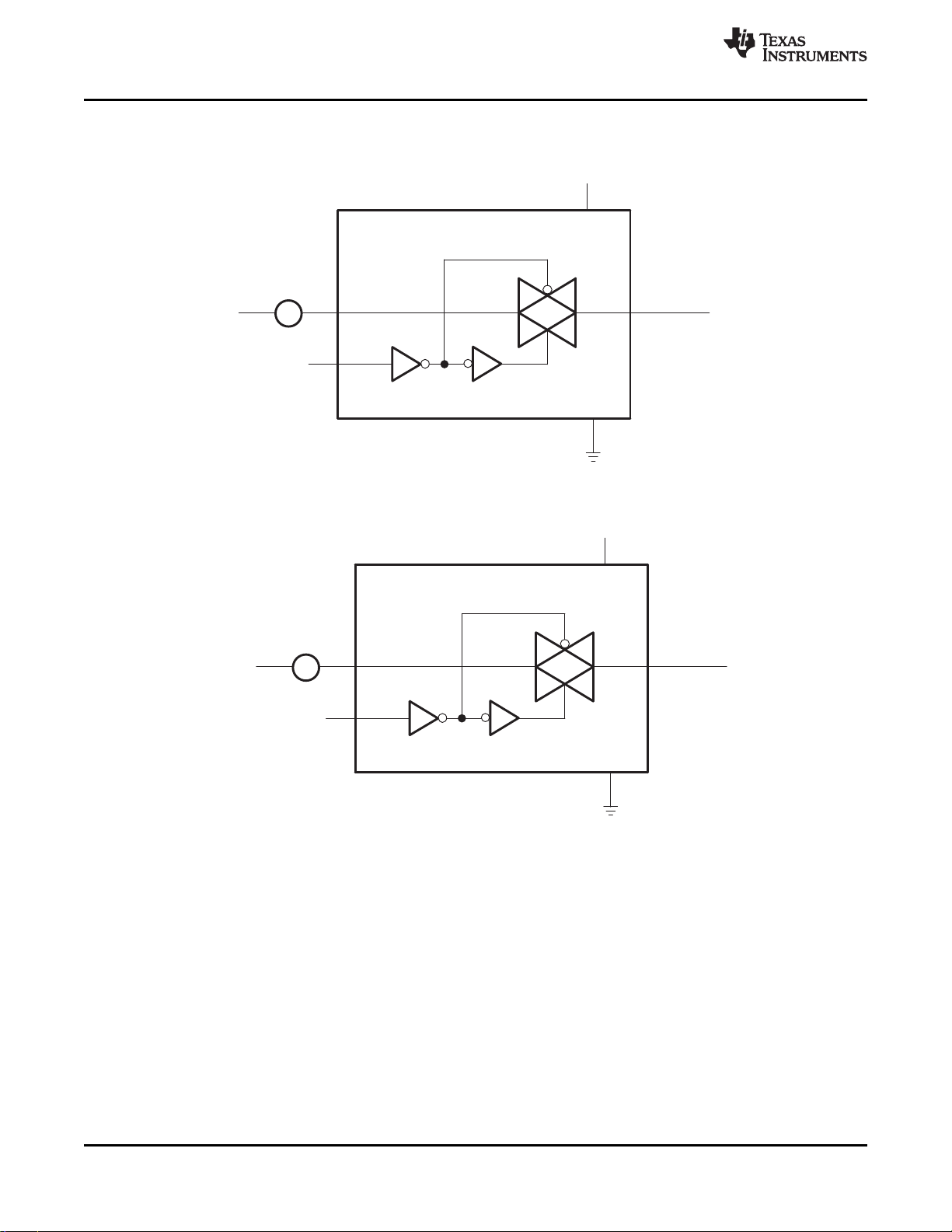
VI = V
CC
or GND
VO = Open
Condition 1: V
I
= GND, VO = V
CC
Condition 2: VI = VCC, VO = GND
V
CC
V
I
V
O
GND(OFF)
B or A
C
A or B
V
CC
V
IL
V
C
A
SN74LVC1G66
SCES323N –JUNE 2001–REVISED NOVEMBER 2012
PARAMETER MEASUREMENT INFORMATION
Figure 3. Off-State Switch Leakage-Current Test Circuit
www.ti.com
Figure 4. On-State Switch Leakage-Current Test Circuit
8 Submit Documentation Feedback Copyright © 2001–2012, Texas Instruments Incorporated
Product Folder Links: SN74LVC1G66
V
M
t
h
t
su
From Output
Under Test
C
L
(see Note A)
LOAD CIRCUIT
S1
V
LOAD
Open
GND
R
L
R
L
Data Input
Timing Input
V
I
0 V
V
I
0 V
0 V
t
w
Input
VOLTAGE WAVEFORMS
SETUP AND HOLD TIMES
VOLTAGE WAVEFORMS
PROPAGATION DELAY TIMES
INVERTING AND NONINVERTING OUTPUTS
VOLTAGE WAVEFORMS
PULSE DURATION
t
PLH
t
PHL
t
PHL
t
PLH
V
OH
V
OH
V
OL
V
OL
V
I
0 V
Input
Output
Waveform 1
S1 at V
LOAD
(see Note B)
Output
Waveform 2
S1 at GND
(see Note B)
V
OL
V
OH
t
PZL
t
PZH
t
PLZ
t
PHZ
V
LOAD
/2
0 V
VOL + V
∆
VOH − V
∆
≈0 V
V
I
VOLTAGE WAVEFORMS
ENABLE AND DISABLE TIMES
LOW- AND HIGH-LEVEL ENABLING
Output
Output
t
PLH/tPHL
t
PLZ/tPZL
t
PHZ/tPZH
Open
V
LOAD
GND
TEST S1
NOTES: A. CL includes probe and jig capacitance.
B. Waveform 1 is for an output with internal conditions such that the output is low, except when disabled by the output control.
Waveform2 is for an output with internal conditions such that the output is high, except when disabled by the output control.
C. All input pulses are supplied by generators having the following characteristics: PRR ≤ 10 MHz, ZO = 50 Ω.
D. The outputs are measured one at a time, with one transition per measurement.
E. t
PLZ
and t
PHZ
are the same as t
dis
.
F. t
PZL
and t
PZH
are the same as ten.
G. t
PLH
and t
PHL
are the same as tpd.
H. All parameters and waveforms are not applicable to all devices.
Output
Control
V
M
V
M
V
M
V
M
V
M
V
M
V
M
V
M
V
M
V
M
V
M
V
M
V
I
V
M
V
M
1.8 V ± 0.15 V
2.5 V ± 0.2 V
3.3 V ± 0.3 V
5 V ± 0.5 V
1 kΩ
500 Ω
500 Ω
500 Ω
V
CC
R
L
2 × V
CC
2 × V
CC
2 × V
CC
2 × V
CC
V
LOAD
C
L
30 pF
30 pF
50 pF
50 pF
0.15 V
0.15 V
0.3 V
0.3 V
V
∆
V
CC
V
CC
V
CC
V
CC
V
I
VCC/2
VCC/2
VCC/2
VCC/2
V
M
tr/t
f
≤2 ns
≤2 ns
≤2.5 ns
≤2.5 ns
INPUTS
SN74LVC1G66
www.ti.com
PARAMETER MEASUREMENT INFORMATION
SCES323N –JUNE 2001–REVISED NOVEMBER 2012
Copyright © 2001–2012, Texas Instruments Incorporated Submit Documentation Feedback 9
Figure 5. Load Circuit and Voltage Waveforms
Product Folder Links: SN74LVC1G66

V
CC
V
O
GND
B or A
C
A or B
V
CC
V
C
C
L
50 pF
50 Ω
VCC/2
VCC/2
R
in
600 Ω
R
L
600 Ω
V
CC
V
O
GND
B or A
C
A or B
V
CC
V
C
V
IH
R
L
C
L
50 Ω
0.1 µF
(ON)
VCC/2
RL/CL: 600 Ω/50 pF
RL/CL: 50 Ω/5 pF
f
in
SN74LVC1G66
SCES323N –JUNE 2001–REVISED NOVEMBER 2012
PARAMETER MEASUREMENT INFORMATION
Figure 6. Frequency Response (Switch ON)
www.ti.com
Figure 7. Crosstalk (Control Input – Switch Output)
10 Submit Documentation Feedback Copyright © 2001–2012, Texas Instruments Incorporated
Product Folder Links: SN74LVC1G66

V
CC
V
O
GND
B or A
C
A or B
V
CC
V
C
V
IH
R
L
10 kΩ
C
L
50 pF
600 Ω
10 µF
(ON)
VCC/2
VCC = 1.65 V , VI = 1.4 V
P-P
VCC = 2.3 V , V
I
= 2 V
P-P
VCC = 3 V , VI = 2.5 V
P-P
VCC = 4.5 V , VI = 4 V
P-P
f
in
10 µF
V
CC
V
O
GND
B or A
C
A or B
V
CC
V
C
V
IL
R
L
C
L
50 Ω
0.1 µF
(OFF)
VCC/2
RL/CL: 600 Ω/50 pF
RL/CL: 50 Ω/5 pF
f
in
R
L
VCC/2
SN74LVC1G66
www.ti.com
SCES323N –JUNE 2001–REVISED NOVEMBER 2012
PARAMETER MEASUREMENT INFORMATION
Figure 8. Feedthrough (Switch OFF)
Copyright © 2001–2012, Texas Instruments Incorporated Submit Documentation Feedback 11
Figure 9. Sine-Wave Distortion
Product Folder Links: SN74LVC1G66

SN74LVC1G66
SCES323N –JUNE 2001–REVISED NOVEMBER 2012
www.ti.com
REVISION HISTORY
Changes from Revision L (January 2007) to Revision M Page
• Added DSF and DRY packge to pin out graphic. ................................................................................................................. 1
• Added Added DSF and DRY package to the ORDERING INFORMATION table. ............................................................... 2
Changes from Revision M (January 2012) to Revision N Page
• Added Jumbo Reel to ORDERING INFORMATION TABLE. ............................................................................................... 2
12 Submit Documentation Feedback Copyright © 2001–2012, Texas Instruments Incorporated
Product Folder Links: SN74LVC1G66

PACKAGE OPTION ADDENDUM
www.ti.com
PACKAGING INFORMATION
Orderable Device Status
SN74LVC1G66DBVR ACTIVE SOT-23 DBV 5 3000 Green (RoHS
SN74LVC1G66DBVRE4 ACTIVE SOT-23 DBV 5 3000 Green (RoHS
SN74LVC1G66DBVRG4 ACTIVE SOT-23 DBV 5 3000 Green (RoHS
SN74LVC1G66DBVT ACTIVE SOT-23 DBV 5 250 Green (RoHS
SN74LVC1G66DBVTE4 ACTIVE SOT-23 DBV 5 250 Green (RoHS
SN74LVC1G66DBVTG4 ACTIVE SOT-23 DBV 5 250 Green (RoHS
SN74LVC1G66DCKR ACTIVE SC70 DCK 5 3000 Green (RoHS
SN74LVC1G66DCKRE4 ACTIVE SC70 DCK 5 3000 Green (RoHS
SN74LVC1G66DCKRG4 ACTIVE SC70 DCK 5 3000 Green (RoHS
SN74LVC1G66DCKT ACTIVE SC70 DCK 5 250 Green (RoHS
SN74LVC1G66DCKTE4 ACTIVE SC70 DCK 5 250 Green (RoHS
SN74LVC1G66DCKTG4 ACTIVE SC70 DCK 5 250 Green (RoHS
SN74LVC1G66DRLR ACTIVE SOT DRL 5 4000 Green (RoHS
SN74LVC1G66DRLRG4 ACTIVE SOT DRL 5 4000 Green (RoHS
SN74LVC1G66DRYR ACTIVE SON DRY 6 5000 Green (RoHS
SN74LVC1G66DSFR ACTIVE SON DSF 6 5000 Green (RoHS
Package Type Package
(1)
Drawing
Pins Package
Qty
& no Sb/Br)
& no Sb/Br)
& no Sb/Br)
& no Sb/Br)
& no Sb/Br)
& no Sb/Br)
& no Sb/Br)
& no Sb/Br)
& no Sb/Br)
& no Sb/Br)
& no Sb/Br)
& no Sb/Br)
& no Sb/Br)
& no Sb/Br)
& no Sb/Br)
& no Sb/Br)
Eco Plan
(2)
Lead/Ball Finish MSL Peak Temp
(3)
CU NIPDAU Level-1-260C-UNLIM -40 to 85 (C662 ~ C665 ~
CU NIPDAU Level-1-260C-UNLIM -40 to 85 (C662 ~ C665 ~
CU NIPDAU Level-1-260C-UNLIM -40 to 85 (C662 ~ C665 ~
CU NIPDAU Level-1-260C-UNLIM -40 to 85 (C665 ~ C66R)
CU NIPDAU Level-1-260C-UNLIM -40 to 85 (C665 ~ C66R)
CU NIPDAU Level-1-260C-UNLIM -40 to 85 (C665 ~ C66R)
CU NIPDAU Level-1-260C-UNLIM -40 to 85 (C65 ~ C6F ~ C6K ~
CU NIPDAU Level-1-260C-UNLIM -40 to 85 (C65 ~ C6F ~ C6K ~
CU NIPDAU Level-1-260C-UNLIM -40 to 85 (C65 ~ C6F ~ C6K ~
CU NIPDAU Level-1-260C-UNLIM -40 to 85 (C65 ~ C6R ~ C6T)
CU NIPDAU Level-1-260C-UNLIM -40 to 85 (C65 ~ C6R ~ C6T)
CU NIPDAU Level-1-260C-UNLIM -40 to 85 (C65 ~ C6R ~ C6T)
CU NIPDAU Level-1-260C-UNLIM -40 to 85 (C67 ~ C6R)
CU NIPDAU Level-1-260C-UNLIM -40 to 85 (C67 ~ C6R)
CU NIPDAU Level-1-260C-UNLIM -40 to 85 C6
CU NIPDAU Level-1-260C-UNLIM -40 to 85 C6
Op Temp (°C) Top-Side Markings
C66R ~ C66T)
C66R ~ C66T)
C66R ~ C66T)
C6O ~ C6R ~
C6T)
C6O ~ C6R ~
C6T)
C6O ~ C6R ~
C6T)
11-Apr-2013
Samples
(4)
Addendum-Page 1
PACKAGE OPTION ADDENDUM
www.ti.com
Orderable Device Status
SN74LVC1G66YZPR ACTIVE DSBGA YZP 5 3000 Green (RoHS
(1)
The marketing status values are defined as follows:
ACTIVE: Product device recommended for new designs.
LIFEBUY: TI has announced that the device will be discontinued, and a lifetime-buy period is in effect.
NRND: Not recommended for new designs. Device is in production to support existing customers, but TI does not recommend using this part in a new design.
PREVIEW: Device has been announced but is not in production. Samples may or may not be available.
OBSOLETE: TI has discontinued the production of the device.
Package Type Package
(1)
Drawing
Pins Package
Qty
Eco Plan
(2)
& no Sb/Br)
Lead/Ball Finish MSL Peak Temp
(3)
SNAGCU Level-1-260C-UNLIM -40 to 85 (C67 ~ C6N)
Op Temp (°C) Top-Side Markings
(4)
11-Apr-2013
(2)
Eco Plan - The planned eco-friendly classification: Pb-Free (RoHS), Pb-Free (RoHS Exempt), or Green (RoHS & no Sb/Br) - please check http://www.ti.com/productcontent for the latest availability
information and additional product content details.
TBD: The Pb-Free/Green conversion plan has not been defined.
Pb-Free (RoHS): TI's terms "Lead-Free" or "Pb-Free" mean semiconductor products that are compatible with the current RoHS requirements for all 6 substances, including the requirement that
lead not exceed 0.1% by weight in homogeneous materials. Where designed to be soldered at high temperatures, TI Pb-Free products are suitable for use in specified lead-free processes.
Pb-Free (RoHS Exempt): This component has a RoHS exemption for either 1) lead-based flip-chip solder bumps used between the die and package, or 2) lead-based die adhesive used between
the die and leadframe. The component is otherwise considered Pb-Free (RoHS compatible) as defined above.
Green (RoHS & no Sb/Br): TI defines "Green" to mean Pb-Free (RoHS compatible), and free of Bromine (Br) and Antimony (Sb) based flame retardants (Br or Sb do not exceed 0.1% by weight
in homogeneous material)
(3)
MSL, Peak Temp. -- The Moisture Sensitivity Level rating according to the JEDEC industry standard classifications, and peak solder temperature.
(4)
Multiple Top-Side Markings will be inside parentheses. Only one Top-Side Marking contained in parentheses and separated by a "~" will appear on a device. If a line is indented then it is a
continuation of the previous line and the two combined represent the entire Top-Side Marking for that device.
Important Information and Disclaimer:The information provided on this page represents TI's knowledge and belief as of the date that it is provided. TI bases its knowledge and belief on information
provided by third parties, and makes no representation or warranty as to the accuracy of such information. Efforts are underway to better integrate information from third parties. TI has taken and
continues to take reasonable steps to provide representative and accurate information but may not have conducted destructive testing or chemical analysis on incoming materials and chemicals.
TI and TI suppliers consider certain information to be proprietary, and thus CAS numbers and other limited information may not be available for release.
In no event shall TI's liability arising out of such information exceed the total purchase price of the TI part(s) at issue in this document sold by TI to Customer on an annual basis.
OTHER QUALIFIED VERSIONS OF SN74LVC1G66 :
Automotive: SN74LVC1G66-Q1
•
Samples
NOTE: Qualified Version Definitions:
Addendum-Page 2

PACKAGE OPTION ADDENDUM
www.ti.com
Automotive - Q100 devices qualified for high-reliability automotive applications targeting zero defects
•
11-Apr-2013
Addendum-Page 3

PACKAGE MATERIALS INFORMATION
www.ti.com 26-Jan-2013
TAPE AND REEL INFORMATION
*All dimensions are nominal
Device Package
Type
SN74LVC1G66DBVR SOT-23 DBV 5 3000 178.0 9.2 3.3 3.2 1.55 4.0 8.0 Q3
SN74LVC1G66DBVT SOT-23 DBV 5 250 178.0 9.2 3.3 3.2 1.55 4.0 8.0 Q3
SN74LVC1G66DCKR SC70 DCK 5 3000 178.0 9.2 2.4 2.4 1.22 4.0 8.0 Q3
SN74LVC1G66DCKR SC70 DCK 5 3000 180.0 9.2 2.3 2.55 1.2 4.0 8.0 Q3
SN74LVC1G66DCKT SC70 DCK 5 250 178.0 9.2 2.4 2.4 1.22 4.0 8.0 Q3
SN74LVC1G66DRLR SOT DRL 5 4000 180.0 9.5 1.78 1.78 0.69 4.0 8.0 Q3
SN74LVC1G66DRLR SOT DRL 5 4000 180.0 8.4 1.98 1.78 0.69 4.0 8.0 Q3
SN74LVC1G66DRYR SON DRY 6 5000 180.0 9.5 1.15 1.6 0.75 4.0 8.0 Q1
SN74LVC1G66DSFR SON DSF 6 5000 180.0 9.5 1.16 1.16 0.5 4.0 8.0 Q2
SN74LVC1G66YZPR DSBGA YZP 5 3000 178.0 9.2 1.02 1.52 0.63 4.0 8.0 Q1
Package
Drawing
Pins SPQ Reel
Diameter
(mm)
Reel
Width
W1 (mm)
A0
(mm)B0(mm)K0(mm)P1(mm)W(mm)
Pin1
Quadrant
Pack Materials-Page 1

PACKAGE MATERIALS INFORMATION
www.ti.com 26-Jan-2013
*All dimensions are nominal
Device Package Type Package Drawing Pins SPQ Length (mm) Width (mm) Height (mm)
SN74LVC1G66DBVR SOT-23 DBV 5 3000 180.0 180.0 18.0
SN74LVC1G66DBVT SOT-23 DBV 5 250 180.0 180.0 18.0
SN74LVC1G66DCKR SC70 DCK 5 3000 180.0 180.0 18.0
SN74LVC1G66DCKR SC70 DCK 5 3000 205.0 200.0 33.0
SN74LVC1G66DCKT SC70 DCK 5 250 180.0 180.0 18.0
SN74LVC1G66DRLR SOT DRL 5 4000 180.0 180.0 30.0
SN74LVC1G66DRLR SOT DRL 5 4000 202.0 201.0 28.0
SN74LVC1G66DRYR SON DRY 6 5000 180.0 180.0 30.0
SN74LVC1G66DSFR SON DSF 6 5000 180.0 180.0 30.0
SN74LVC1G66YZPR DSBGA YZP 5 3000 220.0 220.0 35.0
Pack Materials-Page 2


D: Max =
1.418 mm, Min =
1.358 mm
E: Max =
0.918 mm, Min =
0.858 mm

IMPORTANT NOTICE
Texas Instruments Incorporated and its subsidiaries (TI) reserve the right to make corrections, enhancements, improvements and other
changes to its semiconductor products and services per JESD46, latest issue, and to discontinue any product or service per JESD48, latest
issue. Buyers should obtain the latest relevant information before placing orders and should verify that such information is current and
complete. All semiconductor products (also referred to herein as “components”) are sold subject to TI’s terms and conditions of sale
supplied at the time of order acknowledgment.
TI warrants performance of its components to the specifications applicable at the time of sale, in accordance with the warranty in TI’s terms
and conditions of sale of semiconductor products. Testing and other quality control techniques are used to the extent TI deems necessary
to support this warranty. Except where mandated by applicable law, testing of all parameters of each component is not necessarily
performed.
TI assumes no liability for applications assistance or the design of Buyers’ products. Buyers are responsible for their products and
applications using TI components. To minimize the risks associated with Buyers’ products and applications, Buyers should provide
adequate design and operating safeguards.
TI does not warrant or represent that any license, either express or implied, is granted under any patent right, copyright, mask work right, or
other intellectual property right relating to any combination, machine, or process in which TI components or services are used. Information
published by TI regarding third-party products or services does not constitute a license to use such products or services or a warranty or
endorsement thereof. Use of such information may require a license from a third party under the patents or other intellectual property of the
third party, or a license from TI under the patents or other intellectual property of TI.
Reproduction of significant portions of TI information in TI data books or data sheets is permissible only if reproduction is without alteration
and is accompanied by all associated warranties, conditions, limitations, and notices. TI is not responsible or liable for such altered
documentation. Information of third parties may be subject to additional restrictions.
Resale of TI components or services with statements different from or beyond the parameters stated by TI for that component or service
voids all express and any implied warranties for the associated TI component or service and is an unfair and deceptive business practice.
TI is not responsible or liable for any such statements.
Buyer acknowledges and agrees that it is solely responsible for compliance with all legal, regulatory and safety-related requirements
concerning its products, and any use of TI components in its applications, notwithstanding any applications-related information or support
that may be provided by TI. Buyer represents and agrees that it has all the necessary expertise to create and implement safeguards which
anticipate dangerous consequences of failures, monitor failures and their consequences, lessen the likelihood of failures that might cause
harm and take appropriate remedial actions. Buyer will fully indemnify TI and its representatives against any damages arising out of the use
of any TI components in safety-critical applications.
In some cases, TI components may be promoted specifically to facilitate safety-related applications. With such components, TI’s goal is to
help enable customers to design and create their own end-product solutions that meet applicable functional safety standards and
requirements. Nonetheless, such components are subject to these terms.
No TI components are authorized for use in FDA Class III (or similar life-critical medical equipment) unless authorized officers of the parties
have executed a special agreement specifically governing such use.
Only those TI components which TI has specifically designated as military grade or “enhanced plastic” are designed and intended for use in
military/aerospace applications or environments. Buyer acknowledges and agrees that any military or aerospace use of TI components
which have not been so designated is solely at the Buyer's risk, and that Buyer is solely responsible for compliance with all legal and
regulatory requirements in connection with such use.
TI has specifically designated certain components as meeting ISO/TS16949 requirements, mainly for automotive use. In any case of use of
non-designated products, TI will not be responsible for any failure to meet ISO/TS16949.
Products Applications
Audio www.ti.com/audio Automotive and Transportation www.ti.com/automotive
Amplifiers amplifier.ti.com Communications and Telecom www.ti.com/communications
Data Converters dataconverter.ti.com Computers and Peripherals www.ti.com/computers
DLP® Products www.dlp.com Consumer Electronics www.ti.com/consumer-apps
DSP dsp.ti.com Energy and Lighting www.ti.com/energy
Clocks and Timers www.ti.com/clocks Industrial www.ti.com/industrial
Interface interface.ti.com Medical www.ti.com/medical
Logic logic.ti.com Security www.ti.com/security
Power Mgmt power.ti.com Space, Avionics and Defense www.ti.com/space-avionics-defense
Microcontrollers microcontroller.ti.com Video and Imaging www.ti.com/video
RFID www.ti-rfid.com
OMAP Applications Processors www.ti.com/omap TI E2E Community e2e.ti.com
Wireless Connectivity www.ti.com/wirelessconnectivity
Mailing Address: Texas Instruments, Post Office Box 655303, Dallas, Texas 75265
Copyright © 2013, Texas Instruments Incorporated

 Loading...