Texas Instruments SN74LVC1G14DBVR, SN74LVC1G14DCKR, SN74LVC1G14DRLR, SN74LVC1G14DRY2, SN74LVC1G14DSF2 Schematic [ru]
...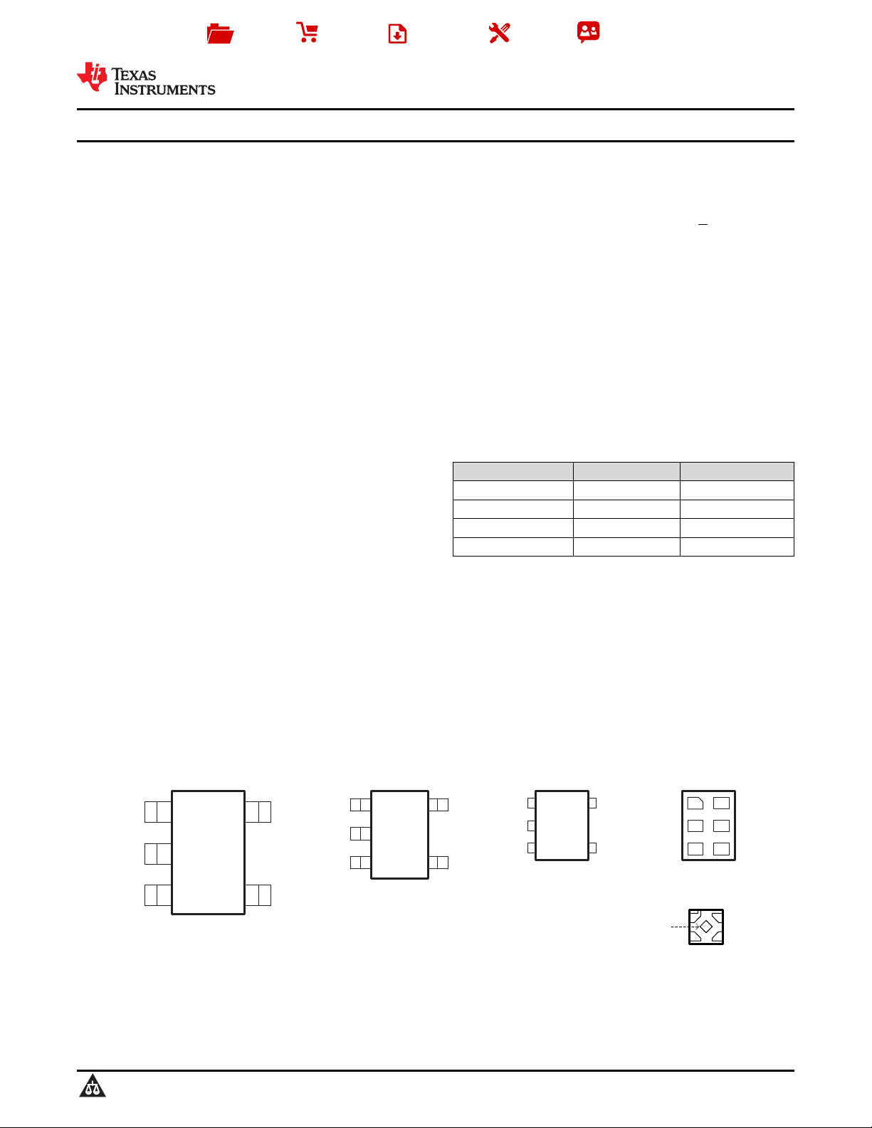
N.C. – No internal connection
See mechanical drawings for dimensions.
DBV PACKAGE
(TOP VIEW)
2
5
3
4
Y
1
A
GND
N.C.
V
CC
DCK PACKAGE
(TOP VIEW)
3
4
2
Y
1
GND
A
N.C.
5
V
CC
DRL PACKAGE
(TOP VIEW)
2
A
1
N.C.
3
4
GND
Y
5
V
CC
DRY PACKAGE
(TOP VIEW)
A
N.C.
N.C.
6
5
4
2
3
GND
Y
V
CC
1
1 5
2
3
A
GND
Y
V
CC
DPW PACKAGE
(TOP VIEW)
B
4
Product
Folder
Sample &
Buy
Technical
Documents
Tools &
Software
Support &
Community
SN74LVC1G14 Single Schmitt-Trigger Inverter
1 Features 3 Description
1
• Available in the Texas Instruments NanoFree™
Package
• Supports 5-V VCCOperation
• Inputs Accept Voltages to 5.5 V
• Max tpdof 4.6 ns at 3.3 V
• Low Power Consumption, 10-μA Max I
CC
• ±24-mA Output Drive at 3.3 V
• I
Supports Partial-Power-Down Mode Operation
off
• Latch-Up Performance Exceeds 100 mA Per
JESD 78, Class II
• ESD Protection Exceeds JESD 22
– 2000-V Human-Body Model (A114-A)
– 200-V Machine Model (A115-A)
– 1000-V Charged-Device Model (C101)
2 Applications
• AV Receiver
• Audio Dock: Portable
• Blu-ray Player and Home Theater
• Embedded PC
• MP3 Player/Recorder (Portable Audio)
• Personal Digital Assistant (PDA)
• Power: Telecom/Server AC/DC Supply: Single
Controller: Analog and Digital
• Solid State Drive (SSD): Client and Enterprise
• TV: LCD/Digital and High-Definition (HDTV)
• Tablet: Enterprise
• Video Analytics: Server
• Wireless Headset, Keyboard, and Mouse
This single Schmitt-trigger inverter is designed for
1.65-V to 5.5-V VCCoperation.
The SN74LVC1G14 device contains one inverter and
performs the Boolean function Y = A. The device
functions as an independent inverter, but because of
Schmitt action, it may have different input threshold
levels for positive-going (VT+) and negative-going
(VT–) signals.
NanoFree™ package technology is a major
breakthrough in IC packaging concepts, using the die
as the package.
This device is fully specified for partial-power-down
applications using I
outputs, preventing damaging current backflow
through the device when it is powered down.
ORDER NUMBER PACKAGE BODY SIZE
SN74LVC1G14DBV SOT-23 (5) 2,9mm × 1,6mm
SN74LVC1G14DCK SC70 (5) 2,0mm × 1,25mm
SN74LVC1G14DRL SOT (5) 1,6mm × 1,2mm
SN74LVC1G14DRY SON (6) 1,45mm × 1,0mm
SN74LVC1G14
SCES218W –APRIL 1999–REVISED MARCH 2014
. The I
off
circuitry disables the
off
Device Information
1
An IMPORTANT NOTICE at the end of this data sheet addresses availability, warranty, changes, use in safety-critical applications,
intellectual property matters and other important disclaimers. PRODUCTION DATA.

SN74LVC1G14
SCES218W –APRIL 1999–REVISED MARCH 2014
www.ti.com
Table of Contents
1 Features.................................................................. 1
2 Applications ........................................................... 1
3 Description ............................................................. 1
4 Revision History..................................................... 2
5 Terminal Configuration and Functions................ 3
6 Specifications......................................................... 4
6.1 Absolute Maximum Ratings ..................................... 4
6.2 Handling Ratings....................................................... 4
6.3 Recommended Operating Conditions ...................... 4
6.4 Electrical Characteristics........................................... 5
6.5 Switching Characteristics ......................................... 6
6.6 Switching Characteristics ......................................... 6
6.7 Operating Characteristics.......................................... 6
7 Parameter Measurement Information .................. 7
8 Device and Documentation Support.................... 9
8.1 Trademarks............................................................... 9
8.2 Electrostatic Discharge Caution................................ 9
8.3 Glossary.................................................................... 9
9 Mechanical, Packaging, and Orderable
Information............................................................. 9
4 Revision History
Changes from Revision V (Novmber 20112) to Revision W Page
• Added DPW Package............................................................................................................................................................. 1
• Added Applications................................................................................................................................................................. 1
• Moved T
to Handling Ratings table..................................................................................................................................... 4
stg
2 Submit Documentation Feedback Copyright © 1999–2014, Texas Instruments Incorporated
Product Folder Links: SN74LVC1G14
A Y
2 4
A Y
1 3
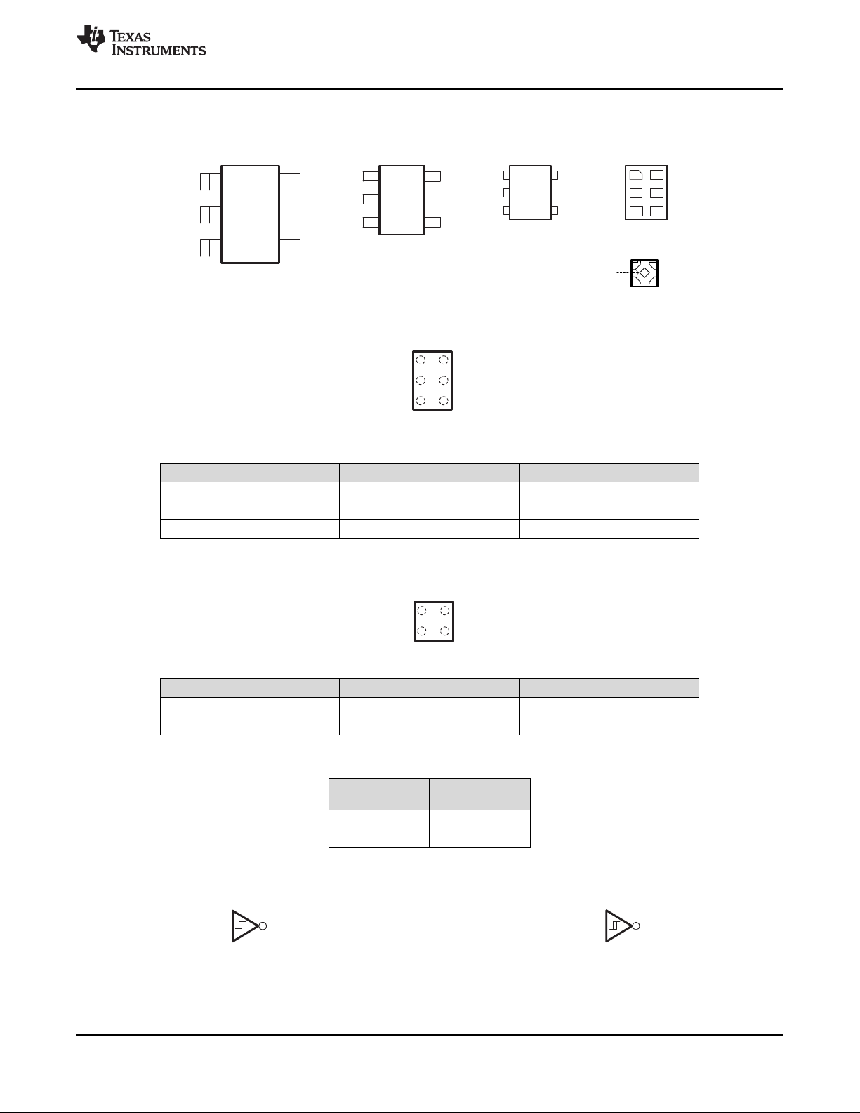
YZV PACKAGE
(TOP VIEW)
A
GND Y
V
CC
A1
A2
B1 B2
DNU – Do not use
YZP PACKAGE
(TOP VIEW)
A
GND
DNU
V
CC
Y
C2C1
B1 B2
A1 A2
N.C. – No internal connection
See mechanical drawings for dimensions.
DBV PACKAGE
(TOP VIEW)
2
5
3
4
Y
1
A
GND
N.C.
V
CC
DCK PACKAGE
(TOP VIEW)
3
4
2
Y
1
GND
A
N.C.
5
V
CC
DRL PACKAGE
(TOP VIEW)
2
A
1
N.C.
3
4
GND
Y
5
V
CC
DRY PACKAGE
(TOP VIEW)
A
N.C.
N.C.
6
5
4
2
3
GND
Y
V
CC
1
1 5
2
3
A
GND
Y
V
CC
DPW PACKAGE
(TOP VIEW)
B
4
www.ti.com
5 Terminal Configuration and Functions
YZP Package Terminal Assignments
A DNU V
B A No ball
C GND Y
SN74LVC1G14
SCES218W –APRIL 1999–REVISED MARCH 2014
1 2
CC
Logic Diagram (Positive Logic) Logic Diagram (Positive Logic)
(DBV, DCK, DRL, DRY, and YZP Package) (YZV Package)
Copyright © 1999–2014, Texas Instruments Incorporated Submit Documentation Feedback 3
YZV Package Terminal Assignments
1 2
A A V
B GND Y
Function Table
INPUT OUTPUT
A Y
H L
L H
Product Folder Links: SN74LVC1G14
CC
SN74LVC1G14
SCES218W –APRIL 1999–REVISED MARCH 2014
6 Specifications
www.ti.com
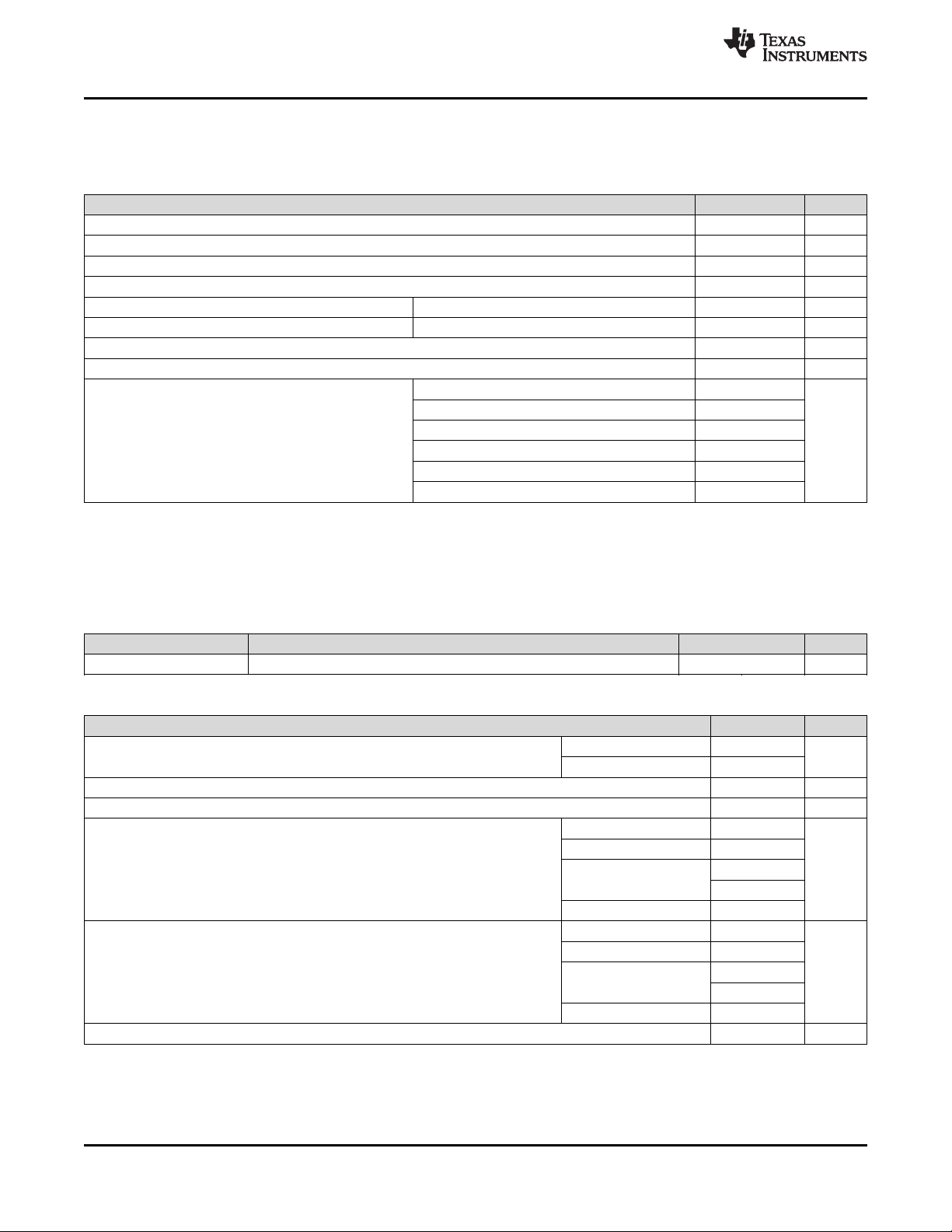
6.1 Absolute Maximum Ratings
(1)
over operating free-air temperature range (unless otherwise noted)
MIN MAX UNIT
V
Supply voltage range –0.5 6.5 V
CC
V
Input voltage range
I
V
Voltage range applied to any output in the high-impedance or power-off state
O
V
Voltage range applied to any output in the high or low state
O
I
Input clamp current VI< 0 –50 mA
IK
I
Output clamp current VO< 0 –50 mA
OK
I
Continuous output current ±50 mA
O
Continuous current through VCCor GND ±100 mA
θ
Package thermal impedance
JA
(1) Stresses beyond those listed under "absolute maximum ratings" may cause permanent damage to the device. These are stress ratings
only, and functional operation of the device at these or any other conditions beyond those indicated under "recommended operating
conditions" is not implied. Exposure to absolute-maximum-rated conditions for extended periods may affect device reliability.
(2) The input and output negative-voltage ratings may be exceeded if the input and output current ratings are observed.
(3) The value of VCCis provided in the recommended operating conditions table.
(4) The package thermal impedance is calculated in accordance with JESD 51-7.
(2)
(2)
(2) (3)
–0.5 6.5 V
–0.5 6.5 V
–0.5 VCC+ 0.5 V
DBV package 206
DCK package 252
(4)
DRL package 142
DRY package 234
°C/W
YZP package 132
YZV package 123
6.2 Handling Ratings
PARAMETER DEFINITION MIN MAX UNIT
T
stg
6.3 Recommended Operating Conditions
V
Supply voltage V
CC
V
Input voltage 0 5.5 V
I
V
Output voltage 0 V
O
I
High-level output current –16 mA
OH
I
Low-level output current 16 mA
OL
T
Operating free-air temperature –40 85 °C
A
(1) All unused inputs of the device must be held at VCCor GND to ensure proper device operation. Refer to the TI application report,
Implications of Slow or Floating CMOS Inputs, literature number SCBA004.
Storage temperature range –65 150 °C
(1)
MIN MAX UNIT
Operating 1.65 5.5
Data retention only 1.5
CC
VCC= 1.65 V –4
VCC= 2.3 V –8
VCC= 3 V
–24
VCC= 4.5 V –32
VCC= 1.65 V 4
VCC= 2.3 V 8
VCC= 3 V
24
VCC= 4.5 V 32
V
4 Submit Documentation Feedback Copyright © 1999–2014, Texas Instruments Incorporated
Product Folder Links: SN74LVC1G14
SN74LVC1G14
www.ti.com
SCES218W –APRIL 1999–REVISED MARCH 2014
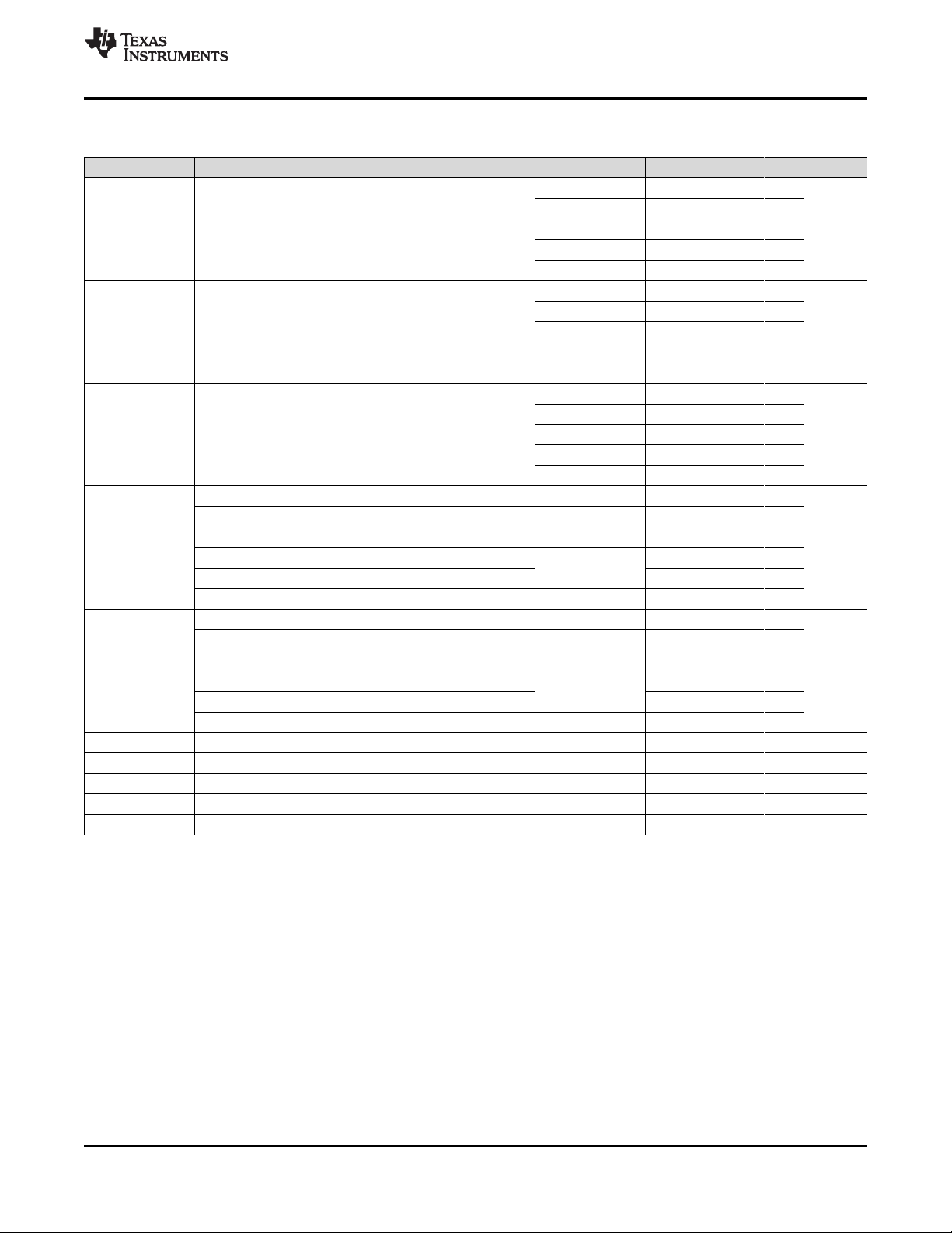
6.4 Electrical Characteristics
over recommended operating free-air temperature range (unless otherwise noted)
PARAMETER TEST CONDITIONS V
CC
MIN TYP
1.65 V 0.79 1.16
V
T+
Positive-going
input threshold
voltage
2.3 V 1.11 1.56
3 V 1.5 1.87 V
4.5 V 2.16 2.74
5.5 V 2.61 3.33
1.65 V 0.39 0.62
V
T–
Negative-going
input threshold
voltage
2.3 V 0.58 0.87
3 V 0.84 1.14 V
4.5 V 1.41 1.79
5.5 V 1.87 2.29
1.65 V 0.37 0.62
ΔV
T
Hysteresis 3 V 0.56 0.87 V
(VT+– VT–)
2.3 V 0.48 0.77
4.5 V 0.71 1.04
5.5 V 0.71 1.11
IOL= –100 μA 1.65 V to 4.5 V VCC– 0.1
IOL= –4 mA 1.65 V 1.2
V
OH
IOL= –8 mA 2.3 V 1.9
IOL= –16 mA 2.4
IOL= –24 mA 2.3
3 V
IOL= –32 mA 4.5 V 3.8
IOL= 100 μA 1.65 V to 4.5 V 0.1
IOL= 4 mA 1.65 V 0.45
V
OL
IOL= 8 mA 2.3 V 0.3
IOL= 16 mA 0.4
IOL= 24 mA 0.55
3 V
IOL= 32 mA 4.5 V 0.55
I
I
I
ΔI
C
A input VI= 5.5 V or GND 0 to 5.5 V ±5 μA
I
off
CC
CC
i
VIor VO= 5.5 V 0 ±10 μA
VI= 5.5 V or GND, IO= 0 1.65 V to 5.5 V 10 μA
One input at VCC– 0.6 V, Other inputs at VCCor GND 3 V to 5.5 V 500 μA
VI= VCCor GND 3.3 V 4.5 pF
(1) All typical values are at VCC= 3.3 V, TA= 25°C.
(1)
MAX UNIT
V
V
Copyright © 1999–2014, Texas Instruments Incorporated Submit Documentation Feedback 5
Product Folder Links: SN74LVC1G14
SN74LVC1G14
SCES218W –APRIL 1999–REVISED MARCH 2014
www.ti.com
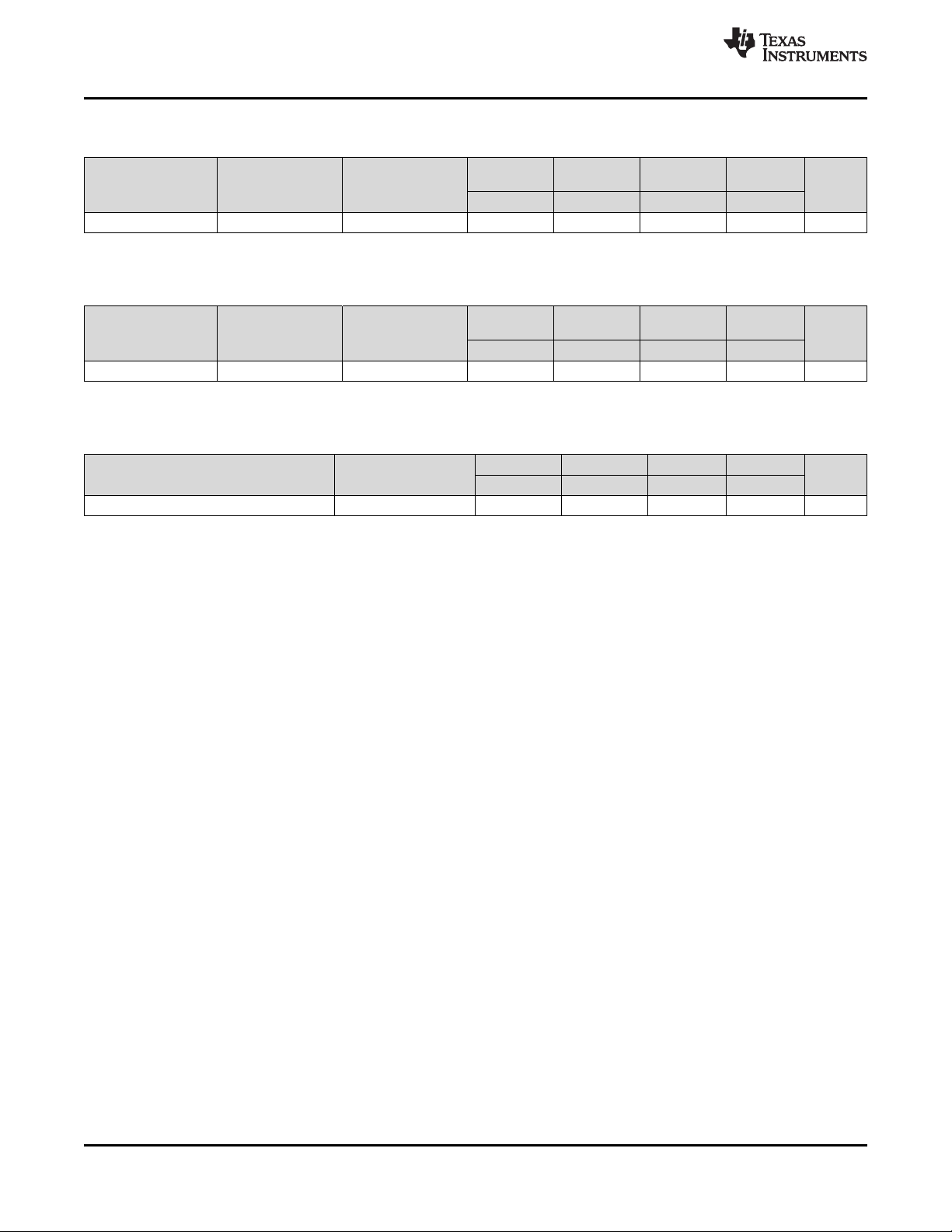
6.5 Switching Characteristics
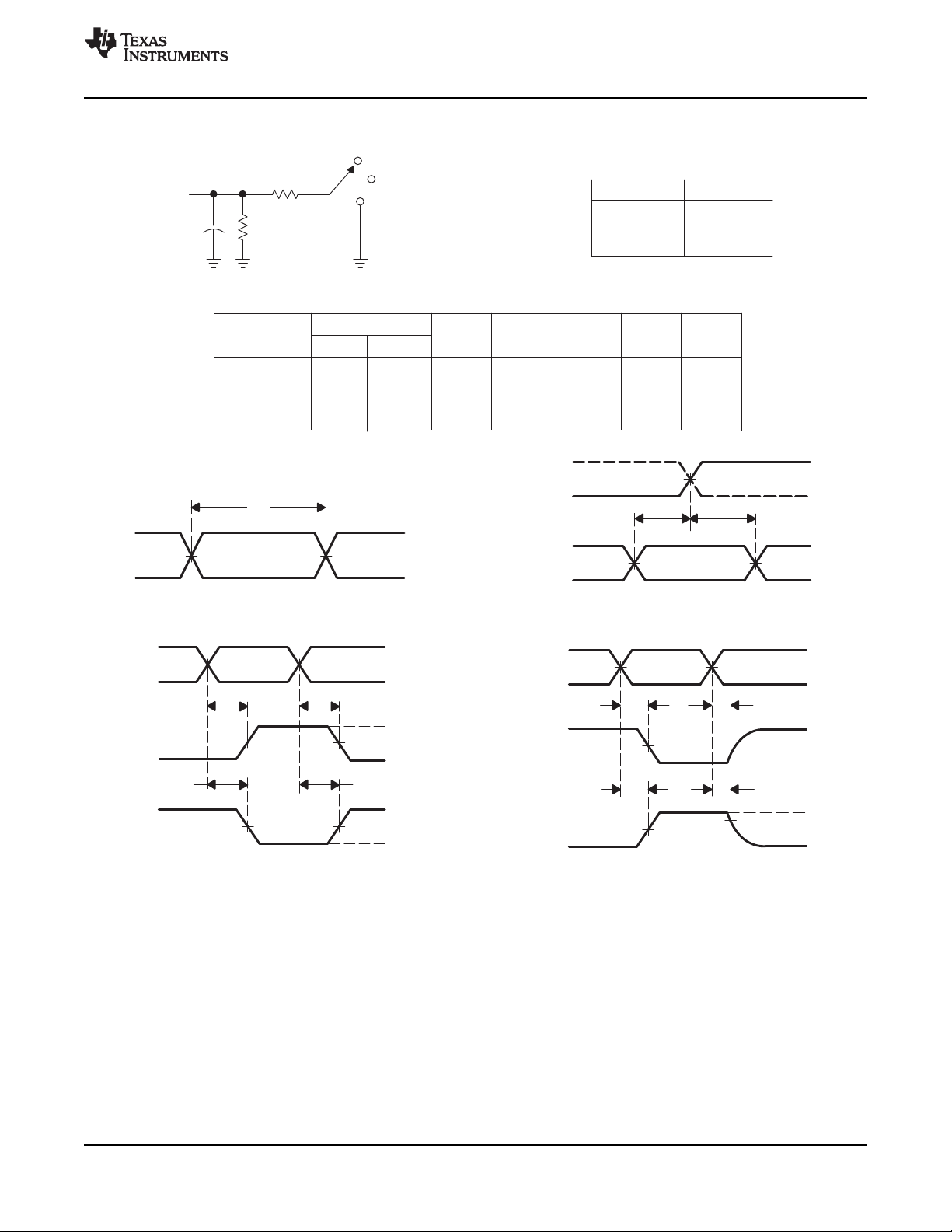
over recommended operating free-air temperature range, CL= 15 pF (unless otherwise noted) (see Figure 1)
PARAMETER UNIT
t
pd
FROM TO
(INPUT) (OUTPUT)
A Y 2.8 9.9 1.6 5.5 1.5 4.6 0.9 4.4 ns
VCC= 1.8 V VCC= 2.5 V VCC= 3.3 V VCC= 5 V
± 0.15 V ± 0.2 V ± 0.3 V ± 0.5 V
MIN MAX MIN MAX MIN MAX MIN MAX
6.6 Switching Characteristics
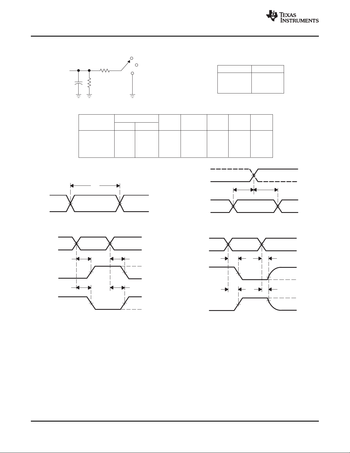
over recommended operating free-air temperature range, CL= 30 pF or 50 pF (unless otherwise noted) (see Figure 2)
PARAMETER UNIT
t
pd
FROM TO
(INPUT) (OUTPUT)
A Y 3.8 11 2 6.5 1.8 5.5 1.2 5 ns
VCC= 1.8 V VCC= 2.5 V VCC= 3.3 V VCC= 5 V
± 0.15 V ± 0.2 V ± 0.3 V ± 0.5 V
MIN MAX MIN MAX MIN MAX MIN MAX
6.7 Operating Characteristics
TA= 25°°C
PARAMETER TEST CONDITIONS UNIT
CpdPower dissipation capacitance f = 10 MHz 20 21 22 25 pF
VCC= 1.8 V VCC= 2.5 V VCC= 3.3 V VCC= 5 V
TYP TYP TYP TYP
6 Submit Documentation Feedback Copyright © 1999–2014, Texas Instruments Incorporated
Product Folder Links: SN74LVC1G14
V
M
t
h
t
su
From Output
Under Test
C
L
(see Note A)
LOAD CIRCUIT
S1
V
LOAD
Open
GND
R
L
R
L
Data Input
Timing Input
V
I
0 V
V
I
0 V
0 V
t
w
Input
VOLTAGE WAVEFORMS
SETUP AND HOLD TIMES
VOLTAGE WAVEFORMS
PROPAGATION DELAY TIMES
INVERTING AND NONINVERTING OUTPUTS
VOLTAGE WAVEFORMS
PULSE DURATION
t
PLH
t
PHL
t
PHL
t
PLH
V
OH
V
OH
V
OL
V
OL
V
I
0 V
Input
Output
Waveform 1
S1 at V
LOAD
(see Note B)
Output
Waveform 2
S1 at GND
(see Note B)
V
OL
V
OH
t
PZL
t
PZH
t
PLZ
t
PHZ
V
LOAD
/2
0 V
VOL + V
∆
VOH − V
∆
≈0 V
V
I
VOLTAGE WAVEFORMS
ENABLE AND DISABLE TIMES
LOW- AND HIGH-LEVEL ENABLING
Output
Output
t
PLH/tPHL
t
PLZ/tPZL
t
PHZ/tPZH
Open
V
LOAD
GND
TEST S1
NOTES: A. CL includes probe and jig capacitance.
B. Waveform 1 is for an output with internal conditions such that the output is low, except when disabled by the output control.
Waveform2 is for an output with internal conditions such that the output is high, except when disabled by the output control.
C. All input pulses are supplied by generators having the following characteristics: PRR ≤ 10 MHz, ZO = 50 Ω.
D. The outputs are measured one at a time, with one transition per measurement.
E. t
PLZ
and t
PHZ
are the same as t
dis
.
F. t
PZL
and t
PZH
are the same as ten.
G. t
PLH
and t
PHL
are the same as tpd.
H. All parameters and waveforms are not applicable to all devices.
Output
Control
V
M
V
M
V
M
V
M
V
M
V
M
V
M
V
M
V
M
V
M
V
M
V
M
V
I
V
M
V
M
1.8 V ± 0.15 V
2.5 V ± 0.2 V
3.3 V ± 0.3 V
5 V ± 0.5 V
1 MΩ
1 MΩ
1 MΩ
1 MΩ
V
CC
R
L
2 × V
CC
2 × V
CC
6 V
2 × V
CC
V
LOAD
C
L
15 pF
15 pF
15 pF
15 pF
0.15 V
0.15 V
0.3 V
0.3 V
V
∆
V
CC
V
CC
3 V
V
CC
V
I
VCC/2
VCC/2
1.5 V
VCC/2
V
M
tr/t
f
≤2 ns
≤2 ns
≤2.5 ns
≤2.5 ns
INPUTS
www.ti.com
7 Parameter Measurement Information
SN74LVC1G14
SCES218W –APRIL 1999–REVISED MARCH 2014
Copyright © 1999–2014, Texas Instruments Incorporated Submit Documentation Feedback 7
Figure 1. Load Circuit and Voltage Waveforms
Product Folder Links: SN74LVC1G14
V
M
t
h
t
su
From Output
Under Test
C
L
(see Note A)
LOAD CIRCUIT
S1
V
LOAD
Open
GND
R
L
R
L
Data Input
Timing Input
V
I
0 V
V
I
0 V
0 V
t
w
Input
VOLTAGE WAVEFORMS
SETUP AND HOLD TIMES
VOLTAGE WAVEFORMS
PROPAGATION DELAY TIMES
INVERTING AND NONINVERTING OUTPUTS
VOLTAGE WAVEFORMS
PULSE DURATION
t
PLH
t
PHL
t
PHL
t
PLH
V
OH
V
OH
V
OL
V
OL
V
I
0 V
Input
Output
Waveform 1
S1 at V
LOAD
(see Note B)
Output
Waveform 2
S1 at GND
(see Note B)
V
OL
V
OH
t
PZL
t
PZH
t
PLZ
t
PHZ
V
LOAD
/2
0 V
VOL + V
∆
VOH − V
∆
≈0 V
V
I
VOLTAGE WAVEFORMS
ENABLE AND DISABLE TIMES
LOW- AND HIGH-LEVEL ENABLING
Output
Output
t
PLH/tPHL
t
PLZ/tPZL
t
PHZ/tPZH
Open
V
LOAD
GND
TEST S1
NOTES: A. CL includes probe and jig capacitance.
B. Waveform 1 is for an output with internal conditions such that the output is low, except when disabled by the output control.
Waveform2 is for an output with internal conditions such that the output is high, except when disabled by the output control.
C. All input pulses are supplied by generators having the following characteristics: PRR ≤ 10 MHz, ZO = 50 Ω.
D. The outputs are measured one at a time, with one transition per measurement.
E. t
PLZ
and t
PHZ
are the same as t
dis
.
F. t
PZL
and t
PZH
are the same as ten.
G. t
PLH
and t
PHL
are the same as tpd.
H. All parameters and waveforms are not applicable to all devices.
Output
Control
V
M
V
M
V
M
V
M
V
M
V
M
V
M
V
M
V
M
V
M
V
M
V
M
V
I
V
M
V
M
1.8 V ± 0.15 V
2.5 V ± 0.2 V
3.3 V ± 0.3 V
5 V ± 0.5 V
1 kΩ
500 Ω
500 Ω
500 Ω
V
CC
R
L
2 × V
CC
2 × V
CC
6 V
2 × V
CC
V
LOAD
C
L
30 pF
30 pF
50 pF
50 pF
0.15 V
0.15 V
0.3 V
0.3 V
V
∆
V
CC
V
CC
3 V
V
CC
V
I
VCC/2
VCC/2
1.5 V
VCC/2
V
M
tr/t
f
≤2 ns
≤2 ns
≤2.5 ns
≤2.5 ns
INPUTS
SN74LVC1G14
SCES218W –APRIL 1999–REVISED MARCH 2014
Parameter Measurement Information (continued)
www.ti.com
8 Submit Documentation Feedback Copyright © 1999–2014, Texas Instruments Incorporated
Figure 2. Load Circuit and Voltage Waveforms
Product Folder Links: SN74LVC1G14

SN74LVC1G14
www.ti.com
SCES218W –APRIL 1999–REVISED MARCH 2014
8 Device and Documentation Support
8.1 Trademarks
NanoFree is a trademark of Texas Instruments.
8.2 Electrostatic Discharge Caution
These devices have limited built-in ESD protection. The leads should be shorted together or the device placed in conductive foam
during storage or handling to prevent electrostatic damage to the MOS gates.
8.3 Glossary
SLYZ022 — TI Glossary.
This glossary lists and explains terms, acronyms and definitions.
9 Mechanical, Packaging, and Orderable Information
The following pages include mechanical packaging and orderable information. This information is the most
current data available for the designated devices. This data is subject to change without notice and revision of
this document. For browser-based versions of this data sheet, refer to the left-hand navigation.
Copyright © 1999–2014, Texas Instruments Incorporated Submit Documentation Feedback 9
Product Folder Links: SN74LVC1G14
 Loading...