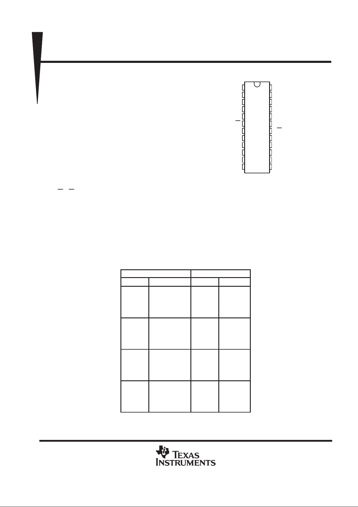
DW OR NT PACKAGE
(TOP VIEW)
1
2
3
4
5
6
7
8
9
10
11
12
24
23
22
21
20
19
18
17
16
15
14
13
S0
1A0
1A1
1A2
1A3
1W
S2
DQA1
DQA2
DQA3
DQA4
GND
V
CC
S1
2A3
2A2
2A1
2A0
2W
S3
DQB4
DQB3
DQB2
DQB1
SN74ALS870
DUAL 16-BY-4 REGISTER FILES
SDAS139A – DECEMBER 1982 – REVISED JANUARY 1995
Copyright 1995, Texas Instruments Incorporated
1
POST OFFICE BOX 655303 • DALLAS, TEXAS 75265
• 3-State Buffer-Type Outputs Drive Bus
Lines Directly
• Each Register File Has Individual
Write-Enable Controls and Address Lines
• Designed Specifically for Multibus
Architecture and Overlapping File
Operations
• Prioritized B-Input Port Prevents Write
Conflicts During Dual-Input Mode
• Package Options Include Plastic
Small-Outline (DW) Packages and Standard
Plastic (NT) 300-mil DIPs
description
This device features two 16-word by 4-bit register
files. Each register file has individual write-enable
(1W
, 2W) controls and address lines. This device has two 4-bit data I/O ports (DQA1–DQA4 and DQB1–DQB4).
The data I/O ports can output to bus A and bus B, receive input from bus A and bus B, receive input from bus
A and output to bus B, or output to bus A and receive input from bus B. To prevent writing conflicts in the
dual-input mode, the B-input port takes priority . Two select (S0 and S1) lines control which port has access to
which register. S2 determines whether the A ports are in the input or the output modes and S3 does likewise
for the B ports. The address lines (1A0–1A3 or 2A0–2A3) are decoded by an internal 1-of-16 decoder to select
which register word is to be accessed. All outputs are 3-state buffer-type outputs designed specifically to drive
bus lines directly.
The SN74ALS870 is characterized for operation from 0°C to 70°C.
FUNCTION TABLE
FILE SELECT
INPUT/OUTPUT
S0 S1 FILE SEL S2 S3 I/O SEL
L L 1R to A, 1R to B
H L 2R to A, 1R to B
L H 1R to A, 2R to B
LLA out, B out
H H 2R to A, 2R to B
L L A to 1R, 1R to B
H L A to 2R, 1R to B
L H A to 1R, 2R to B
HLA in, B out
H H A to 2R, 2R to B
L L 1R to A, B to 1R
H L 2R to A, B to 1R
L H 1R to A, B to 2R
LHA out, B in
H H 2R to A, B to 2R
L L B to 1R
H L A to 2R, B to 1R
L H A to 1R, B to 2R
HHA in, B in
H H B to 2R
PRODUCTION DATA information is current as of publication date.
Products conform to specifications per the terms of Texas Instruments
standard warranty. Production processing does not necessarily include
testing of all parameters.

SN74ALS870
DUAL 16-BY-4 REGISTER FILES
SDAS139A – DECEMBER 1982 – REVISED JANUAR Y 1995
2
POST OFFICE BOX 655303 • DALLAS, TEXAS 75265
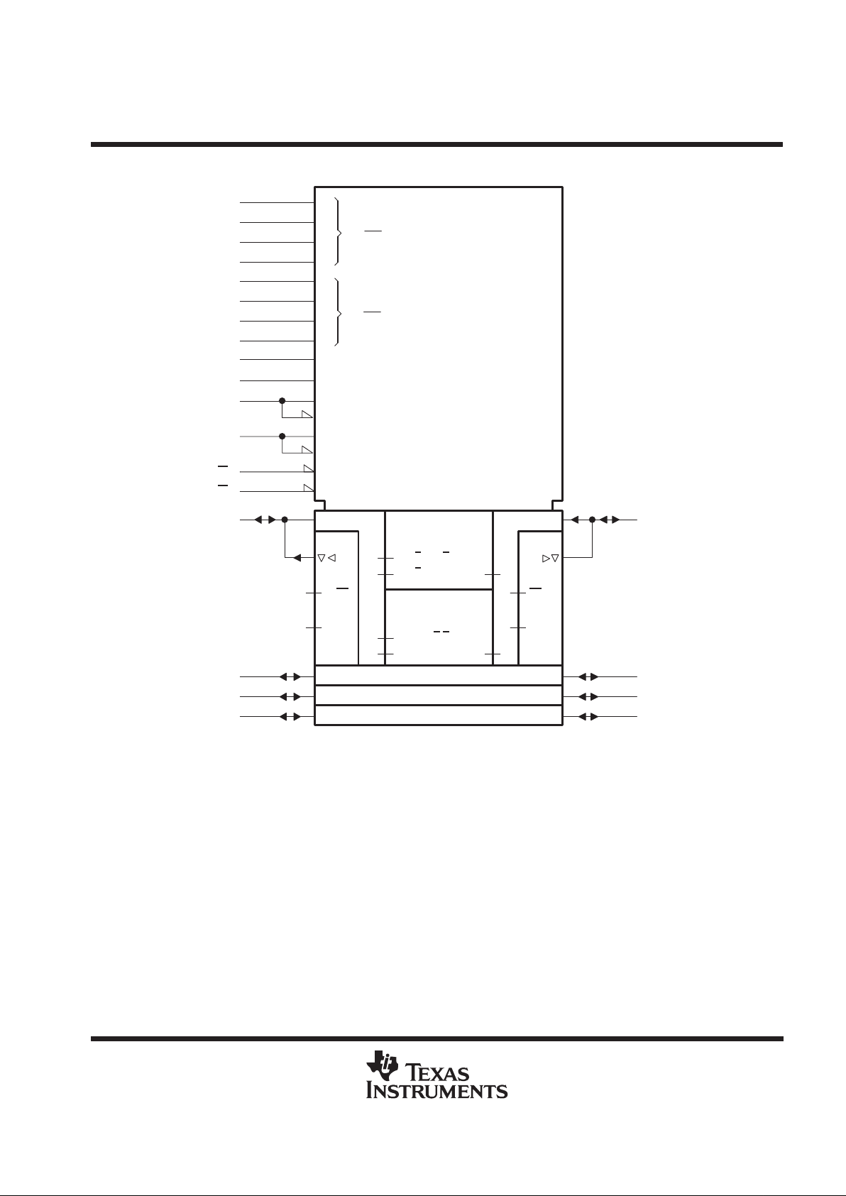
logic symbol
†
DQB2
14
DQB3
15
DQB4
16
DQA2
9
DQA3
10
DQA4
11
1A
0
15
0
2
1A0
3
1A1
4
1A2
3
5
1A3
0
19
2A0
20
2A1
21
2A2
3
22
2A3
C0/G10
1
S0
EN12 [A out]
C4
6
DQB1
13
Z7
C1/G11
23
S1
C2 [A in]
7
S2
C5
18
EN13 [B out]
C3 [B in]
17
S3
1W
2W
9,10
8
9
MUX MUX
[REG FILE 16 × 4]
2A
0
15
12
8,10
11
11
Z8
6
7
RAM 16 × 1
[REG 1]
1A,0
,2(1/3)4D
1A,1
,3,4D
1A
13
Z9
6
7
RAM 16 × 1
[REG 2]
2A,0,2(1
/3)5D
2A,1,3,5D
2A
DQA1
8
Z6
†
This symbol is in accordance with ANSI/IEEE Std 91-1984 and IEC Publication 617-12.

SN74ALS870
DUAL 16-BY-4 REGISTER FILES
SDAS139A – DECEMBER 1982 – REVISED JANUARY 1995
3
POST OFFICE BOX 655303 • DALLAS, TEXAS 75265
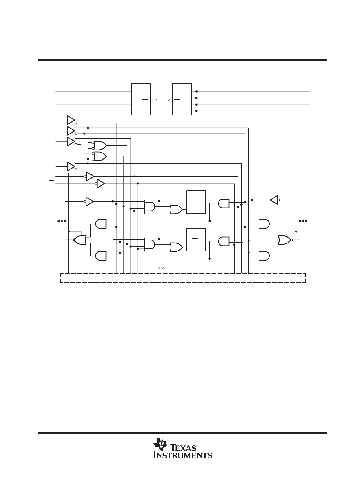
logic diagram (positive logic)
REG1
REG2
Decoder
BIN/Y
16
1
2
3
4
15
0
Decoder
BIN/Y
16
1
2
3
4
15
0
16 16
Three Identical Channels Not Shown
2A0
2A1
2A2
2A3
DQB1
1A0
1A1
1A2
1A3
S0
S1
S2
S3
1W
2W
DQA1
RAM 16×1
A
A,D
15
0
A
A
A,D
15
0
A
RAM 16×1
2
3
4
5
1
23
7
17
6
18
8
19
20
21
22
13
absolute maximum ratings over operating free-air temperature range (unless otherwise noted)
†
Supply voltage, V
CC
7 V. . . . . . . . . . . . . . . . . . . . . . . . . . . . . . . . . . . . . . . . . . . . . . . . . . . . . . . . . . . . . . . . . . . . . . . .
Input voltage, V
I
: All inputs 7 V. . . . . . . . . . . . . . . . . . . . . . . . . . . . . . . . . . . . . . . . . . . . . . . . . . . . . . . . . . . . . . . . . .
I/O ports 5.5 V. . . . . . . . . . . . . . . . . . . . . . . . . . . . . . . . . . . . . . . . . . . . . . . . . . . . . . . . . . . . . . . . .
Voltage applied to a disabled 3-state output 5.5 V. . . . . . . . . . . . . . . . . . . . . . . . . . . . . . . . . . . . . . . . . . . . . . . . . .
Operating free-air temperature range, T
A
0°C to 70°C. . . . . . . . . . . . . . . . . . . . . . . . . . . . . . . . . . . . . . . . . . . . . .
Storage temperature range –65°C to 150°C. . . . . . . . . . . . . . . . . . . . . . . . . . . . . . . . . . . . . . . . . . . . . . . . . . . . . . .
†
Stresses beyond those listed under “absolute maximum ratings” may cause permanent damage to the device. These are stress ratings only, and
functional operation of the device at these or any other conditions beyond those indicated under “recommended operating conditions” is not
implied. Exposure to absolute-maximum-rated conditions for extended periods may affect device reliability.
 Loading...