

Texas Instruments SN74ALS563BDW, SN74ALS563BDWR, SN74ALS563BN, SN74ALS563BN3 Datasheet
FUNCTION TABLE
(each latch)
OUTPUT
Q
OC
CD
H
H
L
X
H
H
X
X
L
L
L
H
L
H
Z
Q
0
1
2
3
4
5
6
7
8
9
10
20
19
18
17
16
15
14
13
12
11
OC
1D
2D
3D
4D
5D
6D
7D
8D
GND
V
CC
1Q
2Q
3Q
4Q
5Q
6Q
7Q
8Q
C
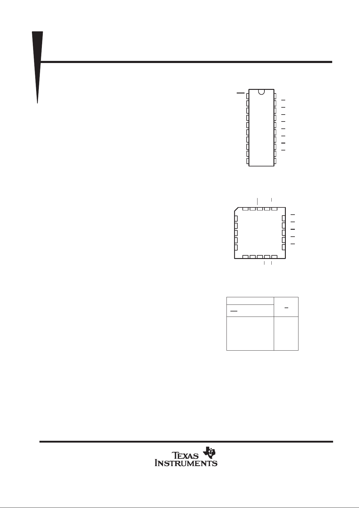
SN54ALS563A . . . J PACKAGE
SN74ALS563B . . . DW OR N PACKAGE
(TOP VIEW)
3 2 1 20 19
910111213
4
5
6
7
8
18
17
16
15
14
2Q
3Q
4Q
5Q
6Q
3D
4D
5D
6D
7D
SN54ALS563A . . . FK PACKAGE
(TOP VIEW)
2D1DOC
8Q
7Q
1Q
8D
GND
C
CC
V
INPUTS
ENABLE
SN54ALS563A, SN74ALS563B
OCTAL D-TYPE TRANSPARENT LATCHES WITH 3-STATE OUTPUTS
SDAS163 – D2661, DECEMBER 1982 – REVISED JANUARY 1989
POST OFFICE BOX 655303 • DALLAS, TEXAS 75265
Copyright 1989, Texas Instruments Incorporated
1
• 3-State Buffer-Type Outputs Drive Bus-Lines
Directly
• Bus Structured Pinout
• Package Options include Plastic Small Outline
Package, Ceramic Chip Carriers and Standard
Plastic and Ceramic DIPs
• Dependable Texas Instruments Quality and
Reliability
description
These 8-bit latches feature three-state outputs
designed specifically for driving highly capacitive
or relatively low-impedance loads. They are
particularly suitable for implementing buffer
registers, I/O ports, bidirectional bus drivers, and
working registers.
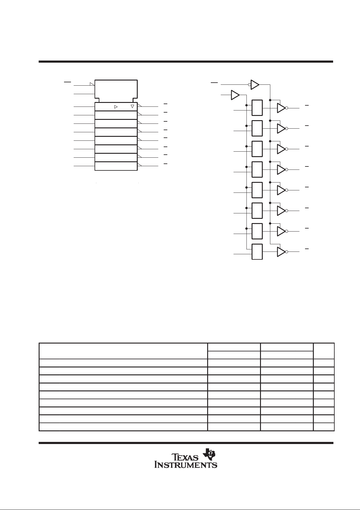
The eight latches are transparent D-type latches.
While the enable (C) is high the Q outputs will
follow the complements of data (D) inputs. When
the enable is taken low the output will be latched
at the inverses of the levels that were set up at the
D inputs.
A buffered output-control input can be used to
place the eight outputs in either a normal logic
state (high or low logic levels) or a
high-impedance state. In the high-impedance
state the outputs neither load nor drive the bus
lines significantly. The high-impedance state and
increased high-logic level provide the capability to
drive the bus lines in a bus-organized system
without need for interface or pull-up components.
The output control (OC) does not affect the
internal operation of the latches. Old data can be
retained or new data can be entered while the
outputs are in the high-impedance state.
The SN54ALS563A is characterized for operation
over the full military temperature range of –55°C
to 125°C. The SN74ALS563B is characterized for
operation from 0°C to 70°C.
PRODUCTION DATA information is current as of publication date.
Products conform to specifications per the terms of Texas Instruments
standard warranty. Production processing does not necessarily include
testing of all parameters.
SN54ALS563A, SN74ALS563B
OCTAL D-TYPE TRANSPARENT LATCHES WITH 3-STATE OUTPUTS
SDAS163 – D2661, DECEMBER 1982 – REVISED JANUARY 1989
POST OFFICE BOX 655303 • DALLAS, TEXAS 75265
2
logic symbol
†
logic diagram (positive logic)
†
This symbol is in accordance with ANSI/IEEE Std 91-1984
and IEC Publication 617-12.
Pin numbers shown are for DW, J, and N packages.
8D
7D
6D
5D
4D
3D
2D
1D
C1
D1
C1
D1
C1
D1
C1
D1
C1
D1
C1
D1
C1
D1
C1
D1
19
2
3
4
5
6
7
8
9
18
17
16
15
12
13
14
1
C
OC
2Q
1Q
4Q
3Q
6Q
5Q
8Q
7Q
11
EN
1
C1
11
C
1D
2
1D
3
2D
4
3D
5
4D
6
5D
19
18
17
16
15
7
6D
8
7D
9
8D
14
13
12
OC
2Q
1Q
4Q
3Q
6Q
5Q
8Q
7Q
absolute maximum ratings over operating free-air temperature range (unless otherwise noted)
Supply voltage, VCC 7 V. . . . . . . . . . . . . . . . . . . . . . . . . . . . . . . . . . . . . . . . . . . . . . . . . . . . . . . . . . . . . . . . . . . . . . . .
Input voltage 7 V. . . . . . . . . . . . . . . . . . . . . . . . . . . . . . . . . . . . . . . . . . . . . . . . . . . . . . . . . . . . . . . . . . . . . . . . . . . . . . .
Voltage applied to a disabled 3-state output 5.5 V. . . . . . . . . . . . . . . . . . . . . . . . . . . . . . . . . . . . . . . . . . . . . . . . . .
Operating free-air temperature range: SN54ALS563A –55°C to 125°C. . . . . . . . . . . . . . . . . . . . . . . . . . . . . .
SN74ALS563B 0°C to 70°C. . . . . . . . . . . . . . . . . . . . . . . . . . . . . . . . . .
Storage temperature range –65°C to 150°C. . . . . . . . . . . . . . . . . . . . . . . . . . . . . . . . . . . . . . . . . . . . . . . . . . . . . . .
recommended operating conditions
SN54ALS563A SN74ALS563B
MIN NOM MAX MIN NOM MAX
UNIT
V
CC
Supply Voltage 4.5 5 5.5 4.5 5 5.5 V
V
IH
High-level input voltage 2 2 V
V
IL
Low-level input voltage 0.7 0.8 V
I
OH
High-level output current –1 –2.6 mA
I
OL
Low-level output current 12 24 mA
t
w
Pulse duration, C high 15 15 ns
t
su
Setup time, data before C↓ 10 10 ns
t
h
Hold time, data after C↓ 10 10 ns
T
A
Operating free-air temperature –55 125 0 70 °C
 Loading...