

Texas Instruments SN74AHC16244DGGR, SN74AHC16244DGVR, SN74AHC16244DL, SN74AHC16244DLR Datasheet
SN54AHC16244, SN74AHC16244
16-BIT BUFFERS/DRIVERS
WITH 3-STATE OUTPUTS
SCLS327G – MARCH 1996 – REVISED JANUARY 2000
D
Members of the Texas Instruments
D
Widebus
EPIC
Family
(Enhanced-Performance Implanted
CMOS) Process
D
Operating Range 2-V to 5.5-V V
D
Distributed VCC and GND Pins Minimize
CC
High-Speed Switching Noise
D
Flow-Through Architecture Optimizes PCB
Layout
D
Latch-Up Performance Exceeds 250 mA Per
JESD 17
D
ESD Protection Exceeds 2000 V Per
MIL-STD-883, Method 3015; Exceeds 200 V
Using Machine Model (C = 200 pF, R = 0)
D
Package Options Include Plastic Shrink
Small-Outline (DL), Thin Shrink
Small-Outline (DGG), and Thin Very
Small-Outline (DGV) Packages and 380-mil
Fine-Pitch Ceramic Flat (WD) Package
Using 25-mil Center-to-Center Spacings
description
The ’AHC16244 devices are 16-bit buffers and
line drivers designed specifically to improve the
performance and density of 3-state memory
address drivers, clock drivers, and bus-oriented
receivers and transmitters.
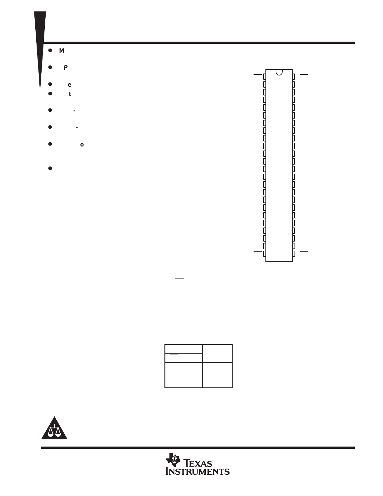
SN54AHC16244 . . . WD PACKAGE
SN74AHC16244 . . . DGG, DGV, OR DL PACKAGE
1OE
1Y1
1Y2
GND
1Y3
1Y4
V
CC
2Y1
2Y2
GND
2Y3
2Y4
3Y1
3Y2
GND
3Y3
3Y4
V
CC
4Y1
4Y2
GND
4Y3
4Y4
4OE
(TOP VIEW)
1
48
2
47
3
46
4
45
5
44
6
43
7
42
8
41
9
40
10
39
11
38
12
37
13
36
14
35
15
34
16
33
17
32
18
31
19
30
20
29
21
28
22
27
23
26
24
25
2OE
1A1
1A2
GND
1A3
1A4
V
CC
2A1
2A2
GND
2A3
2A4
3A1
3A2
GND
3A3
3A4
V
CC
4A1
4A2
GND
4A3
4A4
3OE
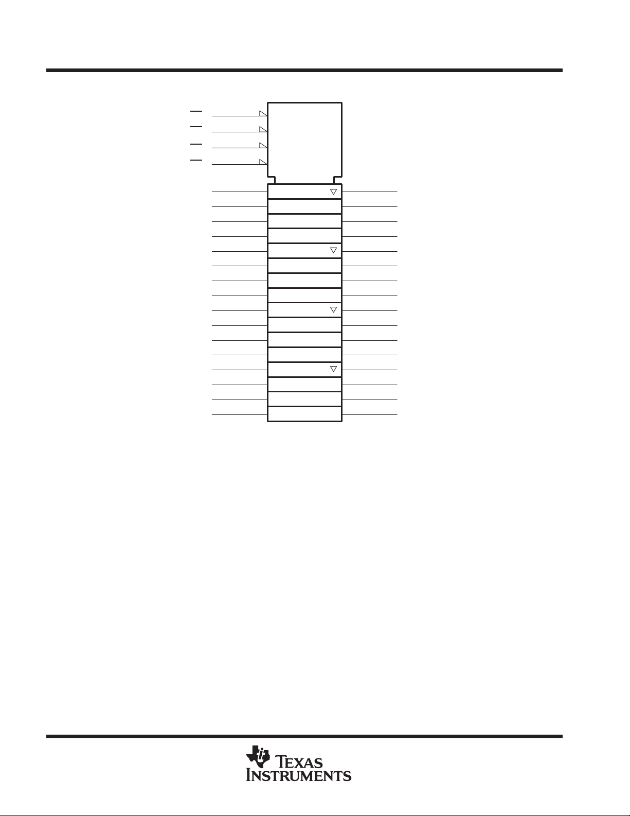
These devices can be used as four 4-bit buffers, two 8-bit buffers, or one 16-bit buffer . They provide true outputs
and symmetrical active-low output-enable (OE) inputs.
T o ensure the high-impedance state during power up or power down, OE should be tied to VCC through a pullup
resistor; the minimum value of the resistor is determined by the current-sinking capability of the driver.
The SN54AHC16244 is characterized for operation over the full military temperature range of –55°C to 125°C.
The SN74AHC16244 is characterized for operation from –40°C to 85°C.
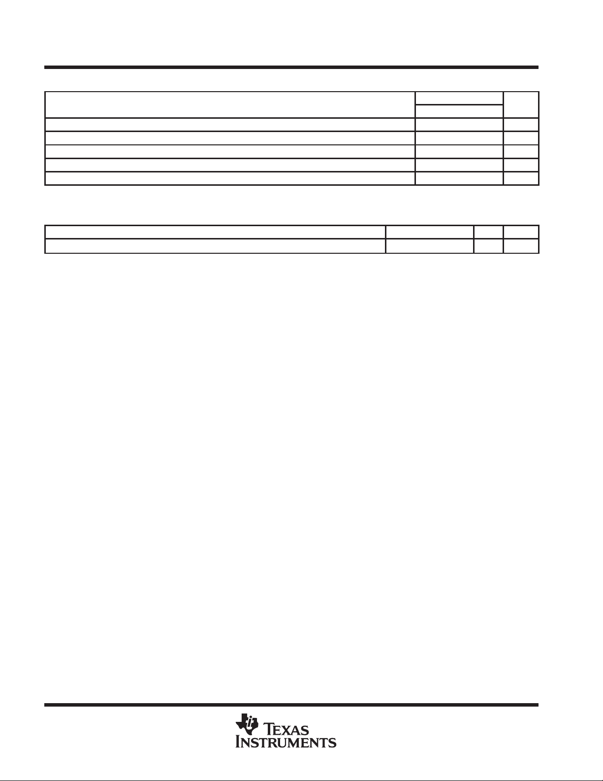
FUNCTION TABLE
(each 4-bit buffer/driver)
INPUTS
OE
L H H
L LL
H X Z
Please be aware that an important notice concerning availability, standard warranty, and use in critical applications of
Texas Instruments semiconductor products and disclaimers thereto appears at the end of this data sheet.
EPIC and Widebus are trademarks of Texas Instruments Incorporated.
UNLESS OTHERWISE NOTED this document contains PRODUCTION
DATA information current as of publication date. Products conform to
specifications per the terms of Texas Instruments standard warranty.
Production processing does not necessarily include testing of all
parameters.
OUTPUT
A
Y
Copyright 2000, Texas Instruments Incorporated
POST OFFICE BOX 655303 • DALLAS, TEXAS 75265
1
SN54AHC16244, SN74AHC16244
16-BIT BUFFERS/DRIVERS
WITH 3-STATE OUTPUTS
SCLS327G – MARCH 1996 – REVISED JANUARY 2000
logic symbol
†
1A1
1A2
1A3
1A4
2A1
2A2
2A3
2A4
3A1
3A2
3A3
3A4
4A1
4A2
4A3
4A4
1
48
25
24
47
46
44
43
41
40
38
37
36
35
33
32
30
29
27
26
EN1
EN2
EN3
EN4
11
12
13
14
16
17
19
20
22
23
2
1Y1
3
1Y2
5
1Y3
6
1Y4
8
2Y1
9
2Y2
2Y3
2Y4
3Y1
3Y2
3Y3
3Y4
4Y1
4Y2
4Y3
4Y4
1
1
1
2
1
3
1
4
1OE
2OE
3OE
4OE
†
This symbol is in accordance with ANSI/IEEE Std 91-1984 and IEC Publication 617-12.
2
POST OFFICE BOX 655303 • DALLAS, TEXAS 75265
logic diagram (positive logic)
SN54AHC16244, SN74AHC16244
16-BIT BUFFERS/DRIVERS
WITH 3-STATE OUTPUTS
SCLS327G – MARCH 1996 – REVISED JANUARY 2000
1OE
1A1
1A2
1A3
1A4
2OE
2A1
2A2
2A3
2A4
1
47
46
44
43
48
41
40
38
37
11
12
25
3OE
2
1Y1
3
1Y2
5
1Y3
6
1Y4
8
2Y1
9
2Y2
2Y3
2Y4
3A1
3A2
3A3
3A4
4OE
4A1
4A2
4A3
4A4
36
35
33
32
24
30
29
27
26
13
14
16
17
19
20
22
23
3Y1
3Y2
3Y3
3Y4
4Y1
4Y2
4Y3
4Y4
absolute maximum ratings over operating free-air temperature range (unless otherwise noted)
Supply voltage range, VCC –0.5 V to 7 V. . . . . . . . . . . . . . . . . . . . . . . . . . . . . . . . . . . . . . . . . . . . . . . . . . . . . . . . . .
Input voltage range, VI (see Note 1) –0.5 V to 7 V. . . . . . . . . . . . . . . . . . . . . . . . . . . . . . . . . . . . . . . . . . . . . . . . . .
Output voltage range, V
Input clamp current, I
Output clamp current, I
Continuous output current, I
(see Note 1) –0.5 V to V
O
(V
< 0) –20 mA. . . . . . . . . . . . . . . . . . . . . . . . . . . . . . . . . . . . . . . . . . . . . . . . . . . . . . . . . . .
IK
I
(V
< 0 or VO > VCC) ±20 mA. . . . . . . . . . . . . . . . . . . . . . . . . . . . . . . . . . . . . . . . . . . .
OK
O
(V
= 0 to VCC) ±25 mA. . . . . . . . . . . . . . . . . . . . . . . . . . . . . . . . . . . . . . . . . . . . . .
O
O
Continuous current through each VCC or GND ±75 mA. . . . . . . . . . . . . . . . . . . . . . . . . . . . . . . . . . . . . . . . . . . . . .
Package thermal impedance, θ
(see Note 2): DGG package 70°C/W. . . . . . . . . . . . . . . . . . . . . . . . . . . . . . .
JA
DGV package 58°C/W. . . . . . . . . . . . . . . . . . . . . . . . . . . . . . . .
DL package 63°C/W. . . . . . . . . . . . . . . . . . . . . . . . . . . . . . . . .
Storage temperature range, T
†
Stresses beyond those listed under “absolute maximum ratings” may cause permanent damage to the device. These are stress ratings only, and
functional operation of the device at these or any other conditions beyond those indicated under “recommended operating conditions” is not
implied. Exposure to absolute-maximum-rated conditions for extended periods may affect device reliability.
NOTES: 1. The input and output voltage ratings may be exceeded if the input and output current ratings are observed.
2. The package thermal impedance is calculated in accordance with JESD 51.
–65°C to 150°C. . . . . . . . . . . . . . . . . . . . . . . . . . . . . . . . . . . . . . . . . . . . . . . . . . .
stg
CC
+ 0.5 V. . . . . . . . . . . . . . . . . . . . . . . . . . . . . . . . . . . . . . . .
†
POST OFFICE BOX 655303 • DALLAS, TEXAS 75265
3

SN54AHC16244, SN74AHC16244
UNIT
mA
mA
∆t/∆vInput transition rise or fall rate
ns/V
PARAMETER
TEST CONDITIONS
V
UNIT
16-BIT BUFFERS/DRIVERS
WITH 3-STATE OUTPUTS
SCLS327G – MARCH 1996 – REVISED JANUARY 2000
recommended operating conditions (see Note 3)
SN54AHC16244 SN74AHC16244
MIN MAX MIN MAX
V
V
V
V
V
I
OH
I
OL
T
NOTE 3: All unused inputs of the device must be held at VCC or GND to ensure proper device operation. Refer to the TI application report,
Supply voltage 2 5.5 2 5.5 V
CC
VCC = 2 V 1.5 1.5
High-level input voltage
IH
Low-level input voltage
IL
Input voltage 0 5.5 0 5.5 V
I
Output voltage 0 V
O
High-level output current
Low-level output current
p
Operating free-air temperature –55 125 –40 85 °C
A
Implications of Slow or Floating CMOS Inputs
, literature number SCBA004.
VCC = 3 V
VCC = 5.5 V 3.85 3.85
VCC = 2 V 0.5 0.5
VCC = 3 V
VCC = 5.5 V 1.65 1.65
VCC = 2 V –50 –50
VCC = 3.3 ± 0.3 V
VCC = 5 ± 0.5 V –8 –8
VCC = 2 V 50 50
VCC = 3.3 ± 0.3 V
VCC = 5 ± 0.5 V 8 8
VCC = 3.3 ± 0.3 V 100 100
VCC = 5 ± 0.5 V 20 20
2.1 2.1
0.9 0.9
CC
–4 –4
4 4
0 V
CC
V
V
V
m
A
m
A
electrical characteristics over recommended operating free-air temperature range (unless
otherwise noted)
CC
2 V 1.9 2 1.9 1.9
IOH = –50 mA
V
OH
IOH = –4 mA 3 V 2.58 2.48 2.48
IOH = –8 mA 4.5 V 3.94 3.8 3.8
IOL = 50 mA
V
OL
IOL = 4 mA 3 V 0.36 0.5 0.44
IOL = 8 mA 4.5 V 0.36 0.5 0.44
I
I
I
OZ
I
CC
C
i
C
o
* On products compliant to MIL-PRF-38535, this parameter is not production tested at VCC = 0 V.
VI = VCC or GND 0 V to 5.5 V ±0.1 ±1* ±1
VO = VCC or GND,
VI (OE
) = VIL or V
VI = VCC or GND, IO = 0 5.5 V 4 40 40
VI = VCC or GND 5 V 2 10 10 pF
VO = VCC or GND 5 V 3.5 pF
IH
3 V 2.9 3 2.9 2.9
4.5 V 4.4 4.5 4.4 4.4
2 V 0.1 0.1 0.1
3 V 0.1 0.1 0.1
4.5 V 0.1 0.1 0.1
5.5 V ±0.25 ±2.5 ±2.5
TA = 25°C SN54AHC16244 SN74AHC16244
MIN TYP MAX MIN MAX MIN MAX
V
V
m
A
m
A
m
A
PRODUCT PREVIEW information concerns products in the formative or
design phase of development. Characteristic data and other
specifications are design goals. Texas Instruments reserves the right to
change or discontinue these products without notice.
4
POST OFFICE BOX 655303 • DALLAS, TEXAS 75265
PARAMETER
UNIT
AYC
15 pF
ns
OE
Y
C
15 pF
ns
OE
Y
C
pF
ns
AYC
50 pF
ns
OE
Y
C
50 pF
ns
OE
Y
C
pF
ns
PARAMETER
UNIT
AYC
pF
ns
OE
Y
C
15 pF
ns
OE
Y
C
pF
ns
AYC
pF
ns
OE
Y
C
50 pF
ns
OE
Y
C
pF
ns
SN54AHC16244, SN74AHC16244
16-BIT BUFFERS/DRIVERS
WITH 3-STATE OUTPUTS
SCLS327G – MARCH 1996 – REVISED JANUARY 2000
switching characteristics over recommended operating free-air temperature range,
V
= 3.3 V ± 0.3 V (unless otherwise noted) (see Figure 1)
CC
FROM TO LOAD
(INPUT) (OUTPUT) CAPACITANCE
t
PLH
t
PHL
t
PZH
t
PZL
t
PHZ
t
PLZ
t
PLH
t
PHL
t
PZH
t
PZL
t
PHZ
t
PLZ
t
sk(o)
* On products compliant to MIL-PRF-38535, this parameter is not production tested.
** On products compliant to MIL-PRF-38535, this parameter does not apply.
CL = 50 pF 1.5
=
L
=
L
= 15
L
=
L
=
L
= 50
L
p
p
p
p
p
p
TA = 25°C SN54AHC16244 SN74AHC16244
MIN TYP MAX MIN MAX MIN MAX
5.8* 8.4* 1* 10* 1 10
5.8* 8.4* 1* 10* 1 10
6.6* 10.6* 1* 12.5* 1 12.5
6.6* 10.6* 1* 12.5* 1 12.5
5* 11.5* 1* 12.5* 1 12.5
5* 11.5* 1* 12.5* 1 12.5
8.3 11.9 1 13.5 1 13.5
8.3 11.9 1 13.5 1 13.5
9.1 14.1 1 16 1 16
9.1 14.1 1 16 1 16
10.3 14 1 16 1 16
10.3 14 1 16 1 16
**
1.5 ns
switching characteristics over recommended operating free-air temperature range,
V
= 5 V ± 0.5 V (unless otherwise noted) (see Figure 1)
CC
FROM TO LOAD
(INPUT) (OUTPUT) CAPACITANCE
t
PLH
t
PHL
t
PZH
t
PZL
t
PHZ
t
PLZ
t
PLH
t
PHL
t
PZH
t
PZL
t
PHZ
t
PLZ
t
sk(o)
* On products compliant to MIL-PRF-38535, this parameter is not production tested.
** On products compliant to MIL-PRF-38535, this parameter does not apply.
CL = 50 pF 1
= 15
L
=
L
= 15
L
= 50
L
=
L
= 50
L
p
p
p
p
p
p
TA = 25°C SN54AHC16244 SN74AHC16244
MIN TYP MAX MIN MAX MIN MAX
3.9* 6* 1* 7* 1 6.5
3.9* 6* 1* 7* 1 6.5
4.7* 7.3* 1* 8.5* 1 8.5
4.7* 7.3* 1* 8.5* 1 8.5
5* 7.2* 1* 8.5* 1 8.5
5* 7.2* 1* 8.5* 1 8.5
5.4 8 1 9 1 8.5
5.4 8 1 9 1 8.5
6.2 9.3 1 10.5 1 10.5
6.2 9.3 1 10.5 1 10.5
6.7 9.2 1 10.5 1 10.5
6.7 9.2 1 10.5 1 10.5
**
1 ns
PRODUCT PREVIEW information concerns products in the formative or
design phase of development. Characteristic data and other
specifications are design goals. Texas Instruments reserves the right to
change or discontinue these products without notice.
POST OFFICE BOX 655303 • DALLAS, TEXAS 75265
5
SN54AHC16244, SN74AHC16244
PARAMETER
UNIT
16-BIT BUFFERS/DRIVERS
WITH 3-STATE OUTPUTS
SCLS327G – MARCH 1996 – REVISED JANUARY 2000
noise characteristics, V
V
OL(P)
V
OL(V)
V
OH(V)
V
IH(D)
V
IL(D)
NOTE 4: Characteristics are for surface-mount packages only.
Quiet output, maximum dynamic V
Quiet output, minimum dynamic V
Quiet output, minimum dynamic V
High-level dynamic input voltage 3.5 V
Low-level dynamic input voltage 1.5 V
operating characteristics, V
C
Power dissipation capacitance No load, f = 1 MHz 10.5 pF
pd
= 5 V, CL = 50 pF, TA = 25°C (see Note 4)
CC
OL
OL
OH
= 5 V, TA = 25°C
CC
PARAMETER TEST CONDITIONS TYP UNIT
SN74AHC16244
MIN TYP MAX
0.5 V
–0.2 V
4.8 V
6
POST OFFICE BOX 655303 • DALLAS, TEXAS 75265

From Output
Under Test
(see Note A)
SN54AHC16244, SN74AHC16244
16-BIT BUFFERS/DRIVERS
WITH 3-STATE OUTPUTS
SCLS327G – MARCH 1996 – REVISED JANUARY 2000
PARAMETER MEASUREMENT INFORMATION
V
Test
Point
C
L
From Output
Under Test
(see Note A)
C
L
RL = 1 kΩ
S1
CC
Open
GND
TEST S1
t
PLH/tPHL
t
PLZ/tPZL
t
PHZ/tPZH
Open Drain
Open
V
CC
GND
V
CC
LOAD CIRCUIT FOR
TOTEM-POLE OUTPUTS
Input
VOLTAGE WAVEFORMS
Input
t
PLH
In-Phase
Output
t
PHL
Out-of-Phase
Output
VOLTAGE WAVEFORMS
PROPAGATION DELAY TIMES
INVERTING AND NONINVERTING OUTPUTS
t
w
50% V
CC
PULSE DURATION
50% V
CC
50% V
50% V
3-STATE AND OPEN-DRAIN OUTPUTS
50% V
50% V
CC
CC
LOAD CIRCUIT FOR
V
CC
CC
0 V
V
CC
CC
0 V
t
PHL
V
t
PLH
CC
V
V
CC
V
OH
OL
OH
OL
50% V
50% V
Timing Input
(see Note B)
(see Note B)
Data Input
Output
Control
Output
Waveform 1
S1 at V
CC
Output
Waveform 2
S1 at GND
50% V
CC
t
CC
CC
h
50% V
50% V
VOL + 0.3 V
VOH – 0.3 V
CC
t
t
CC
PLZ
PHZ
t
su
50% V
CC
VOLTAGE WAVEFORMS
SETUP AND HOLD TIMES
50% V
CC
t
PZL
50% V
t
PZH
50% V
VOLTAGE WAVEFORMS
ENABLE AND DISABLE TIMES
LOW- AND HIGH-LEVEL ENABLING
V
CC
0 V
V
CC
0 V
V
CC
0 V
≈V
V
OL
V
OH
≈0 V
CC
NOTES: A. CL includes probe and jig capacitance.
B. Waveform 1 is for an output with internal conditions such that the output is low except when disabled by the output control.
Waveform 2 is for an output with internal conditions such that the output is high except when disabled by the output control.
C. All input pulses are supplied by generators having the following characteristics: PRR ≤ 1 MHz, ZO = 50 Ω, tr ≤ 3 ns, tf ≤ 3 ns.
D. The outputs are measured one at a time with one input transition per measurement.
Figure 1. Load Circuit and Voltage Waveforms
POST OFFICE BOX 655303 • DALLAS, TEXAS 75265
7

IMPORTANT NOTICE
T exas Instruments and its subsidiaries (TI) reserve the right to make changes to their products or to discontinue
any product or service without notice, and advise customers to obtain the latest version of relevant information
to verify, before placing orders, that information being relied on is current and complete. All products are sold
subject to the terms and conditions of sale supplied at the time of order acknowledgement, including those
pertaining to warranty, patent infringement, and limitation of liability.
TI warrants performance of its semiconductor products to the specifications applicable at the time of sale in
accordance with TI’s standard warranty. Testing and other quality control techniques are utilized to the extent
TI deems necessary to support this warranty . Specific testing of all parameters of each device is not necessarily
performed, except those mandated by government requirements.
CERTAIN APPLICA TIONS USING SEMICONDUCT OR PRODUCTS MAY INVOLVE POTENTIAL RISKS OF
DEATH, PERSONAL INJURY, OR SEVERE PROPERTY OR ENVIRONMENTAL DAMAGE (“CRITICAL
APPLICATIONS”). TI SEMICONDUCTOR PRODUCTS ARE NOT DESIGNED, AUTHORIZED, OR
WARRANTED TO BE SUITABLE FOR USE IN LIFE-SUPPORT DEVICES OR SYSTEMS OR OTHER
CRITICAL APPLICA TIONS. INCLUSION OF TI PRODUCTS IN SUCH APPLICATIONS IS UNDERST OOD TO
BE FULLY AT THE CUSTOMER’S RISK.
In order to minimize risks associated with the customer’s applications, adequate design and operating
safeguards must be provided by the customer to minimize inherent or procedural hazards.
TI assumes no liability for applications assistance or customer product design. TI does not warrant or represent
that any license, either express or implied, is granted under any patent right, copyright, mask work right, or other
intellectual property right of TI covering or relating to any combination, machine, or process in which such
semiconductor products or services might be or are used. TI’s publication of information regarding any third
party’s products or services does not constitute TI’s approval, warranty or endorsement thereof.
Copyright 2000, Texas Instruments Incorporated
 Loading...