

Texas Instruments SN74AC241DBLE, SN74AC241DBR, SN74AC241DW, SN74AC241DWR, SN74AC241N Datasheet
...
SN54AC241, SN74AC241
OCTAL BUFFERS/DRIVERS
WITH 3-STATE OUTPUTS
SCAS513C – JUNE 1995 – REVISED SEPTEMBER 1996
D
EPIC
(Enhanced-Performance Implanted
CMOS) 1-µm Process
D
Package Options Include Plastic
Small-Outline (DW), Shrink Small-Outline
(DB), and Thin Shrink Small-Outline (PW)
Packages, Ceramic Chip Carriers (FK), Flat
(W), and DIP (J, N) Packages
description
These octal buffers and line drivers are designed
specifically to improve the performance and
density of 3-state memory address drivers, clock
drivers, and bus-oriented receivers and
transmitters.
The ’AC241 are organized as two 4-bit
buffers/drivers with separate complementary
output-enable (1OE
is low or 2OE is high, the device passes
noninverted data from the A inputs to the Y
outputs. When 1OE
outputs are in the high-impedance state.
The SN54AC241 is characterized for operation
over the full military temperature range of –55°C
to 125°C. The SN74AC241 is characterized for
operation from –40°C to 85°C.
and 2OE) inputs. When 1OE
is high or 2OE is low, the
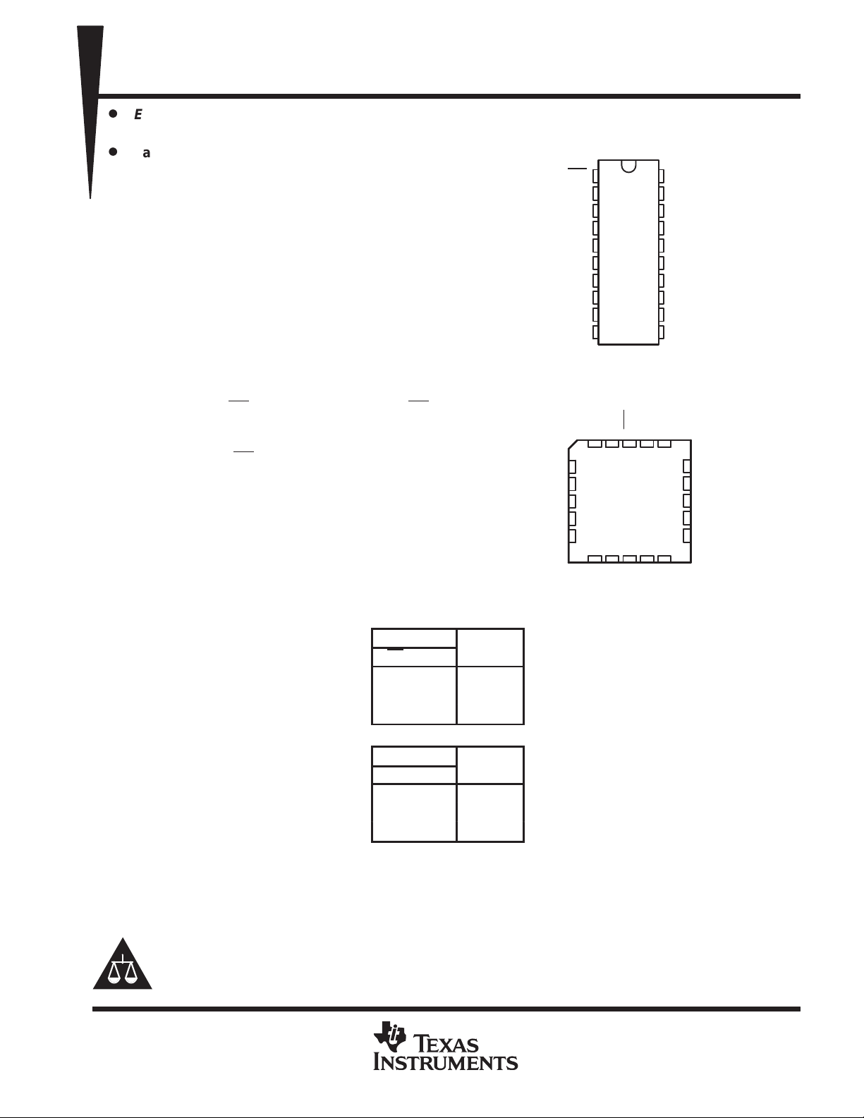
SN54AC241 ...J OR W PACKAGE
SN74AC241 . . . DB, DW, N, OR PW PACKAGE
SN54AC241 . . . FK PACKAGE
1A2
2Y3
1A3
2Y2
1A4
1OE
1A1
2Y4
1A2
2Y3
1A3
2Y2
1A4
2Y1
GND
3 2 1 20 19
4
5
6
7
8
9 10 11 12 13
(TOP VIEW)
1
20
2
19
3
18
4
17
5
16
6
15
7
14
8
13
9
12
10
11
(TOP VIEW)
1A1
V
1OE
2Y4
CC
V
CC
2OE
1Y1
2A4
1Y2
2A3
1Y3
2A2
1Y4
2A1
18
17
16
15
14
1Y1
2A4
1Y2
2A3
1Y3
1Y4
2A1
2A2 2OE
2Y1
GND
FUNCTION TABLES
INPUTS
1OE 1A
L H H
L LL
H X Z
INPUTS
2OE 2A
H H H
H LL
L X Z
Please be aware that an important notice concerning availability, standard warranty, and use in critical applications of
Texas Instruments semiconductor products and disclaimers thereto appears at the end of this data sheet.
OUTPUT
1Y
OUTPUT
2Y
EPIC is a trademark of Texas Instruments Incorporated.
UNLESS OTHERWISE NOTED this document contains PRODUCTION
DATA information current as of publication date. Products conform to
specifications per the terms of Texas Instruments standard warranty.
Production processing does not necessarily include testing of all
parameters.
POST OFFICE BOX 655303 • DALLAS, TEXAS 75265
Copyright 1996, Texas Instruments Incorporated
1
SN54AC241, SN74AC241
OCTAL BUFFERS/DRIVERS
WITH 3-STATE OUTPUTS
SCAS513C – JUNE 1995 – REVISED SEPTEMBER 1996
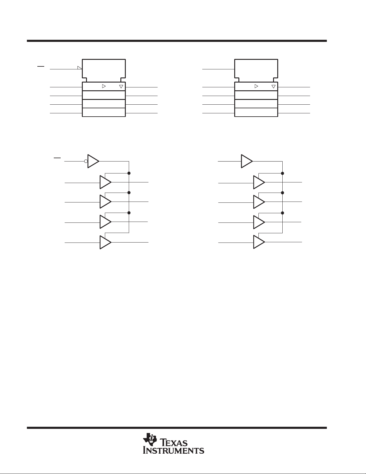
logic symbol
1OE
1A1
1A2
1A3
1A4
†
This symbol is in accordance with ANSI/IEEE Std 91-1984 and IEC Publication 617-12.
†
1
2
4
6
8
EN
18
16
14
12
1Y1
1Y2
1Y3
1Y4
2OE
2A1
2A2
2A3
2A4
logic diagram (positive logic)
1
1OE
1A1
1A2
1A3
2
4
6
18
16
14
1Y1
1Y2
1Y3
19
11
13
15
17
2OE
2A1
2A2
2A3
19
11
13
15
EN
9
2Y1
7
2Y2
5
2Y3
3
2Y4
9
2Y1
7
2Y2
5
2Y3
1A4
8
12
1Y4
2A4
17
3
2Y4
absolute maximum ratings over operating free-air temperature range (unless otherwise noted)
Supply voltage range, VCC –0.5 V to 7 V. . . . . . . . . . . . . . . . . . . . . . . . . . . . . . . . . . . . . . . . . . . . . . . . . . . . . . . . . .
Input voltage range, VI (see Note 1) –0.5 V to VCC + 0.5 V. . . . . . . . . . . . . . . . . . . . . . . . . . . . . . . . . . . . . . . . . . .
Output voltage range, V
Input clamp current, IIK (VI < 0 or VI > VCC) ±20 mA. . . . . . . . . . . . . . . . . . . . . . . . . . . . . . . . . . . . . . . . . . . . . . . .
Output clamp current, IOK (VO < 0 or VO > VCC) ±20 mA. . . . . . . . . . . . . . . . . . . . . . . . . . . . . . . . . . . . . . . . . . . .
Continuous output current, IO (VO = 0 to VCC) ±50 mA. . . . . . . . . . . . . . . . . . . . . . . . . . . . . . . . . . . . . . . . . . . . . .
Continuous current through VCC or GND ±200 mA. . . . . . . . . . . . . . . . . . . . . . . . . . . . . . . . . . . . . . . . . . . . . . . . . .
Maximum power dissipation at T
Storage temperature range, T
‡
Stresses beyond those listed under “absolute maximum ratings” may cause permanent damage to the device. These are stress ratings only, and
functional operation of the device at these or any other conditions beyond those indicated under “recommended operating conditions” is not
implied. Exposure to absolute-maximum-rated conditions for extended periods may affect device reliability.
NOTES: 1. The input and output voltage ratings may be exceeded if the input and output current ratings are observed.
2. The maximum package power dissipation is calculated using a junction temperature of 150°C and a board trace length of 750 mils,
except for the N package, which has a trace length of zero.
(see Note 1) –0.5 V to VCC + 0.5 V. . . . . . . . . . . . . . . . . . . . . . . . . . . . . . . . . . . . . . . .
O
= 55°C (in still air) (see Note 2): DB package 0.6 W. . . . . . . . . . . . . . . . . .
A
DW package 1.6 W. . . . . . . . . . . . . . . . . .
N package 1.3 W. . . . . . . . . . . . . . . . . . . .
PW package 0.7 W. . . . . . . . . . . . . . . . . .
–65°C to 150°C. . . . . . . . . . . . . . . . . . . . . . . . . . . . . . . . . . . . . . . . . . . . . . . . . . .
stg
‡
2
POST OFFICE BOX 655303 • DALLAS, TEXAS 75265
 Loading...