

Texas Instruments SN74ABT2241DBLE, SN74ABT2241DBR, SN74ABT2241DW, SN74ABT2241DWR, SN74ABT2241N Datasheet
...
SN54ABT2241, SN74ABT2241
OCTAL BUFFERS AND LINE/MOS DRIVERS
WITH 3-STATE OUTPUTS
SCBS233B – JANUARY 1991 – REVISED JANUARY 1997
1
POST OFFICE BOX 655303 • DALLAS, TEXAS 75265
D
Output Ports Have Equivalent 25-Ω Series
Resistors, So No External Resistors Are
Required
D
State-of-the-Art
EPIC-ΙΙB
BiCMOS Design
Significantly Reduces Power Dissipation
D
T ypical V
OLP
(Output Ground Bounce)
< 1 V at VCC = 5 V, TA = 25°C
D
Package Options Include Plastic
Small-Outline (DW), Shrink Small-Outline
(DB), and Thin Shrink Small-Outline (PW)
Packages, Ceramic Chip Carriers (FK), and
Plastic (N) and Ceramic (J) DIPs
description
These octal buffers and line drivers are designed
specifically to improve both the performance and
density of 3-state memory address drivers, clock
drivers, and bus-oriented receivers and
transmitters. Together with the SN54ABT2240,
SN74ABT2240A and ’ABT2244A, these devices
provide the choice of selected combinations of
inverting and noninverting outputs, symmetrical
active-low output-enable (OE
) inputs, and
complementary OE and OE inputs. These devices
feature high fan-out and improved fan-in.
The outputs, which are designed to sink up to
12 mA, include equivalent 25-Ω series resistors to
reduce overshoot and undershoot.
T o ensure the high-impedance state during power up or power down, OE should be tied to VCC through a pullup
resistor; the minimum value of the resistor is determined by the current-sinking capability of the driver. OE
should be tied to GND through a pulldown resistor; the minimum value of the resistor is determined by the
current-sourcing capability of the driver.
The SN54ABT2241 is characterized for operation over the full military temperature range of –55°C to 125°C.
The SN74ABT2241 is characterized for operation from –40°C to 85°C.
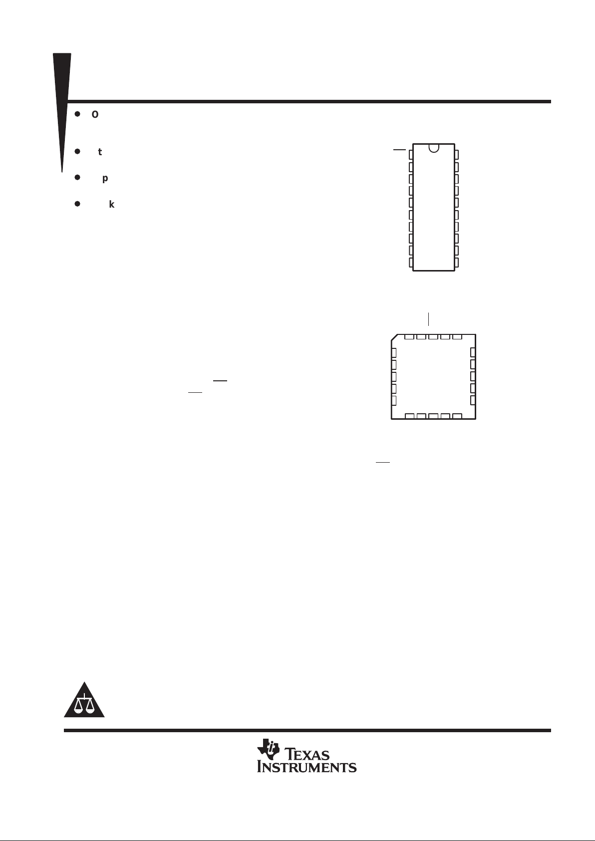
SN54ABT2241 ...J PACKAGE
SN74ABT2241 . . . DB, DW, N, OR PW PACKAGE
(TOP VIEW)
1
2
3
4
5
6
7
8
9
10
20
19
18
17
16
15
14
13
12
11
1OE
1A1
2Y4
1A2
2Y3
1A3
2Y2
1A4
2Y1
GND
V
CC
2OE
1Y1
2A4
1Y2
2A3
1Y3
2A2
1Y4
2A1
3212019
910111213
4
5
6
7
8
18
17
16
15
14
1Y1
2A4
1Y2
2A3
1Y3
1A2
2Y3
1A3
2Y2
1A4
SN54ABT2241 . . . FK PACKAGE
(TOP VIEW)
2Y4
1A1
1OE
1Y4
2A2 2OE
2Y1
GND
2A1
V
CC
Copyright 1997, Texas Instruments Incorporated
UNLESS OTHERWISE NOTED this document contains PRODUCTION
DATA information current as of publication date. Products conform to
specifications per the terms of Texas Instruments standard warranty.
Production processing does not necessarily include testing of all
parameters.
EPIC-ΙΙB is a trademark of Texas Instruments Incorporated.
Please be aware that an important notice concerning availability, standard warranty, and use in critical applications of
Texas Instruments semiconductor products and disclaimers thereto appears at the end of this data sheet.
SN54ABT2241, SN74ABT2241
OCTAL BUFFERS AND LINE/MOS DRIVERS
WITH 3-STATE OUTPUTS
SCBS233B – JANUARY 1991 – REVISED JANUARY 1997
2
POST OFFICE BOX 655303 • DALLAS, TEXAS 75265
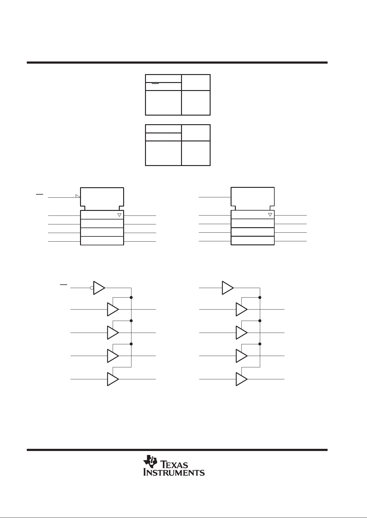
FUNCTION TABLES
INPUTS
OUTPUT
1OE 1A
1Y
L H H
L LL
H X Z
INPUTS
OUTPUT
2OE 2A
2Y
H H H
H LL
L X Z
logic symbol
†
2
1A1
4
1A2
6
1A3
8
1A4
EN
1
1Y1
18
1Y2
16
1Y3
14
1Y4
12
11
2A1
13
2A2
15
2A3
17
2A4
EN
19
2OE
2Y1
9
2Y2
7
2Y3
5
2Y4
3
1OE
†
This symbol is in accordance with ANSI/IEEE Std 91-1984 and IEC Publication 617-12.
11
logic diagram (positive logic)
1
218
1Y1
1OE
1A1
416
1Y2
1A2
614
1Y3
1A3
812
1Y4
1A4
19
11 9
2Y1
2OE
2A1
13 7
2Y2
2A2
15 5
2Y3
2A3
17 3
2Y4
2A4
SN54ABT2241, SN74ABT2241
OCTAL BUFFERS AND LINE/MOS DRIVERS
WITH 3-STATE OUTPUTS
SCBS233B – JANUARY 1991 – REVISED JANUARY 1997
3
POST OFFICE BOX 655303 • DALLAS, TEXAS 75265
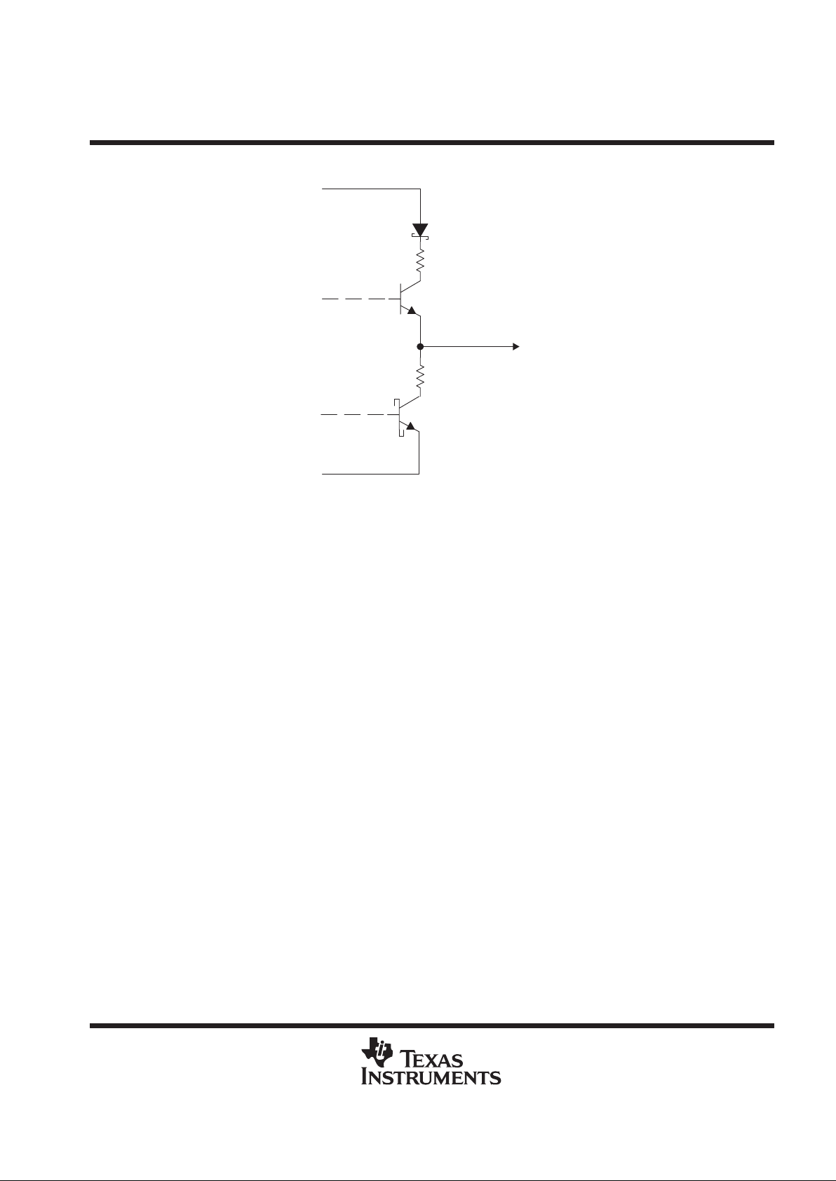
schematic of Y outputs
Output
V
CC
GND
absolute maximum ratings over operating free-air temperature range (unless otherwise noted)
†
Supply voltage range, VCC –0.5 V to 7 V. . . . . . . . . . . . . . . . . . . . . . . . . . . . . . . . . . . . . . . . . . . . . . . . . . . . . . . . . .
Input voltage range, V
I
(see Note 1) –0.5 V to 7 V. . . . . . . . . . . . . . . . . . . . . . . . . . . . . . . . . . . . . . . . . . . . . . . . . .
Voltage range applied to any output in the high or power-off state, VO –0.5 V to 5.5 V. . . . . . . . . . . . . . . . . . .
Current into any output in the low state, IO 30 mA. . . . . . . . . . . . . . . . . . . . . . . . . . . . . . . . . . . . . . . . . . . . . . . . . .
Input clamp current, I
IK
(V
I
< 0) –18 mA. . . . . . . . . . . . . . . . . . . . . . . . . . . . . . . . . . . . . . . . . . . . . . . . . . . . . . . . . . .
Output clamp current, I
OK
(V
O
< 0) –50 mA. . . . . . . . . . . . . . . . . . . . . . . . . . . . . . . . . . . . . . . . . . . . . . . . . . . . . . . .
Package thermal impedance, θ
JA
(see Note 2): DB package 115°C/W. . . . . . . . . . . . . . . . . . . . . . . . . . . . . . . . .
DW package 97°C/W. . . . . . . . . . . . . . . . . . . . . . . . . . . . . . . . .
N package 67°C/W. . . . . . . . . . . . . . . . . . . . . . . . . . . . . . . . . . .
PW package 128°C/W. . . . . . . . . . . . . . . . . . . . . . . . . . . . . . . .
Storage temperature range, T
stg
–65°C to 150°C. . . . . . . . . . . . . . . . . . . . . . . . . . . . . . . . . . . . . . . . . . . . . . . . . . .
†
Stresses beyond those listed under “absolute maximum ratings” may cause permanent damage to the device. These are stress ratings only, and
functional operation of the device at these or any other conditions beyond those indicated under “recommended operating conditions” is not
implied. Exposure to absolute-maximum-rated conditions for extended periods may affect device reliability.
NOTES: 1. The input and output negative-voltage ratings may be exceeded if the input and output clamp-current ratings are observed.
2. The package thermal impedance is calculated in accordance with EIA/JEDEC Std JESD51, except for through-hole packages,
which use a trace length of zero.
 Loading...