

Texas Instruments SN74ABT162823ADGGR, SN74ABT162823ADL, SN74ABT162823ADLR Datasheet
SN54ABT162823A, SN74ABT162823A
18-BIT BUS-INTERFACE FLIP-FLOPS
WITH 3-STATE OUTPUTS
SCBS666A – JULY 1996 – REVISED MAY 1997
D
Members of the Texas Instruments
Widebus
D
Output Ports Have Equivalent 25-Ω Series
Family
Resistors So No External Resistors Are
Required
D
State-of-the-Art
EPIC-ΙΙB
BiCMOS Design
Significantly Reduces Power Dissipation
D
High-Impedance State During Power Up
and Power Down
D
T ypical V
(Output Ground Bounce) < 1 V
OLP
at VCC = 5 V, TA = 25°C
D
Distributed VCC and GND Pin Configuration
Minimizes High-Speed Switching Noise
D
Flow-Through Architecture Optimizes PCB
Layout
D
Package Options Include Plastic 300-mil
Shrink Small-Outline (DL) Package and
380-mil Fine-Pitch Ceramic Flat (WD)
Package Using 25-mil Center-to-Center
Spacings
description
These 18-bit bus-interface flip-flops feature
3-state outputs designed specifically for driving
highly capacitive or relatively low-impedance
loads. They are particularly suitable for
implementing wider buffer registers, I/O ports,
bidirectional bus drivers with parity, and working
registers.
The ’ABT162823A can be used as two 9-bit
flip-flops or one 18-bit flip-flop. With the
clock-enable (CLKEN
flip-flops enter data on the low-to-high transitions
of the clock. Taking CLKEN high disables the
clock buffer , thus latching the outputs. Taking the
clear (CLR
) input low causes the Q outputs to go
low independently of the clock.
) input low, the D-type
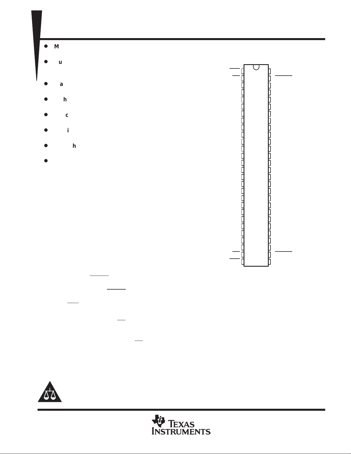
SN54ABT162823A . . . WD PACKAGE
SN74ABT162823A . . . DL PACKAGE
1CLR
1OE
1Q1
GND
1Q2
1Q3
V
CC
1Q4
1Q5
1Q6
GND
1Q7
1Q8
1Q9
2Q1
2Q2
2Q3
GND
2Q4
2Q5
2Q6
V
CC
2Q7
2Q8
GND
2Q9
2OE
2CLR
(TOP VIEW)
1
56
2
55
3
54
4
53
5
52
6
51
7
50
8
49
9
48
10
47
11
46
12
45
13
44
14
43
15
42
16
41
17
40
18
39
19
38
20
37
21
36
22
35
23
34
24
33
25
32
26
31
27
30
28
29
1CLK
1CLKEN
1D1
GND
1D2
1D3
V
CC
1D4
1D5
1D6
GND
1D7
1D8
1D9
2D1
2D2
2D3
GND
2D4
2D5
2D6
V
CC
2D7
2D8
GND
2D9
2CLKEN
2CLK
A buffered output-enable (OE) input places the nine outputs in either a normal logic state (high or low level) or
a high-impedance state. In the high-impedance state, the outputs neither load nor drive the bus lines
significantly. The high-impedance state and increased drive provide the capability to drive bus lines without
interface or pullup components. OE does not affect the internal operation of the flip-flops. Old data can be
retained or new data can be entered while the outputs are in the high-impedance state.
The outputs, which are designed to source or sink up to 12 mA, include equivalent 25-Ω series resistors to
reduce overshoot and undershoot.
Please be aware that an important notice concerning availability, standard warranty, and use in critical applications of
Texas Instruments semiconductor products and disclaimers thereto appears at the end of this data sheet.
Widebus and EPIC-ΙΙB are trademarks of Texas Instruments Incorporated.
UNLESS OTHERWISE NOTED this document contains PRODUCTION
DATA information current as of publication date. Products conform to
specifications per the terms of Texas Instruments standard warranty.
Production processing does not necessarily include testing of all
parameters.
POST OFFICE BOX 655303 • DALLAS, TEXAS 75265
Copyright 1997, Texas Instruments Incorporated
1
SN54ABT162823A, SN74ABT162823A
18-BIT BUS-INTERFACE FLIP-FLOPS
WITH 3-STATE OUTPUTS
SCBS666A – JULY 1996 – REVISED MAY 1997
description (continued)
When VCC is between 0 and 2.1 V , the device is in the high-impedance state during power up or power down.
However, to ensure the high-impedance state above 2.1 V, OE should be tied to VCC through a pullup resistor;
the minimum value of the resistor is determined by the current-sinking capability of the driver.
The SN54ABT162823A is characterized for operation over the full military temperature range of –55°C to
125°C. The SN74ABT162823A is characterized for operation from –40°C to 85°C.
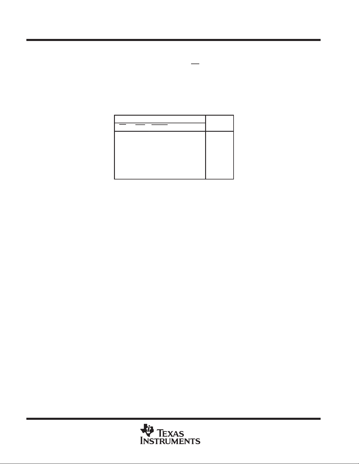
FUNCTION TABLE
(each 9-bit flip-flop)
INPUTS
OE
CLR CLKEN
L L X X X L
L HL↑ HH
L HL↑ LL
L HLLX Q
L HHXX Q
H X X X X Z
CLK D
OUTPUT
Q
0
0
2
POST OFFICE BOX 655303 • DALLAS, TEXAS 75265
SN54ABT162823A, SN74ABT162823A
18-BIT BUS-INTERFACE FLIP-FLOPS
WITH 3-STATE OUTPUTS
SCBS666A – JULY 1996 – REVISED MAY 1997
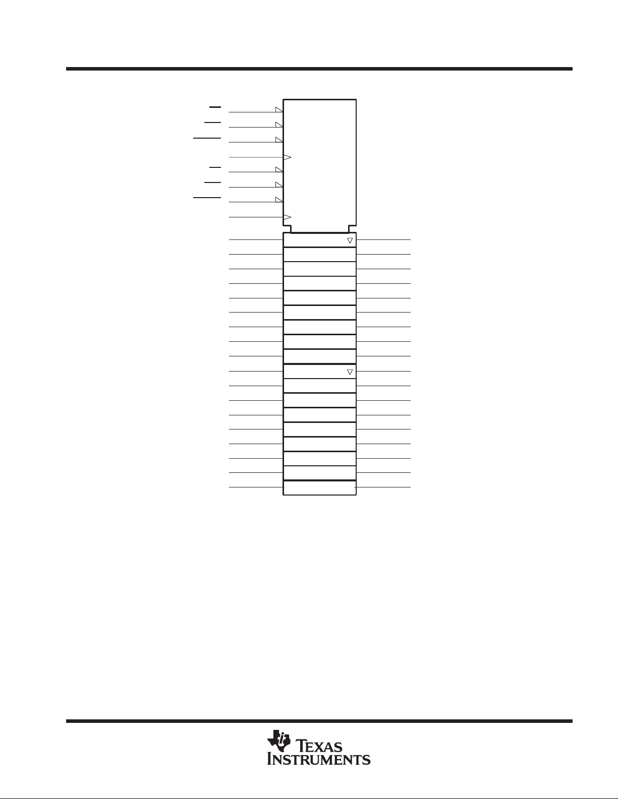
logic symbol
†
2
1OE
1CLR
1CLKEN
1CLK 3C4
2CLR
2CLKEN
2CLK
1
55
56
27
2OE
28
30
29
54
1D1 1Q1
52
1D2 1Q2
51
1D3 1Q3
49
1D4
48
1D5
47
1D6
45
1D7
44
1D8
43
1D9 1Q9
42
2D1 2Q1
41
2D2
40
2D3 2Q3
38
2D4
37
2D5
36
2D6
34
2D7 2Q7
33
2D8 2Q8
31
2D9 2Q9
EN1
R2
G3
EN5
R6
G7
4D
8D
7C8
1, 2
5, 6
10
12
13
14
15
16
17
19
20
21
23
24
26
3
5
6
8
1Q4
9
1Q5
1Q6
1Q7
1Q8
2Q2
2Q4
2Q5
2Q6
†
This symbol is in accordance with ANSI/IEEE Std 91-1984 and IEC Publication 617-12.
POST OFFICE BOX 655303 • DALLAS, TEXAS 75265
3
 Loading...