

Texas Instruments SN74ABT162601DGGR, SN74ABT162601DL, SN74ABT162601DLR Datasheet
SN54ABT162601, SN74ABT162601
18-BIT UNIVERSAL BUS TRANSCEIVERS
WITH 3-STATE OUTPUTS
SCBS247G – AUGUST 1992 – REVISED JUL Y 1998
1
POST OFFICE BOX 655303 • DALLAS, TEXAS 75265
D
Members of the Texas Instruments
Widebus
Family
D
B-Port Outputs Have Equivalent 25-Ω
Series Resistors, So No External Resistors
Are Required
D
State-of-the-Art
EPIC-ΙΙB
BiCMOS Design
Significantly Reduces Power Dissipation
D
UBT
(Universal Bus Transceiver)
Combines D-Type Latches and D-Type
Flip-Flops for Operation in Transparent,
Latched, Clocked, or Clock-Enabled Mode
D
Latch-Up Performance Exceeds 500 mA Per
JESD 17
D
T ypical V
OLP
(Output Ground Bounce)
< 0.8 V at V
CC
= 5 V, TA = 25°C
D
High-Impedance State During Power Up
and Power Down
D
Flow-Through Architecture Optimizes PCB
Layout
D
Package Options Include Plastic 300-mil
Shrink Small-Outline (DL) and Thin Shrink
Small-Outline (DGG) Packages and 380-mil
Fine-Pitch Ceramic Flat (WD) Package
Using 25-mil Center-to-Center Spacings
description
These 18-bit universal bus transceivers combine
D-type latches and D-type flip-flops to allow data
flow in transparent, latched, and clocked modes.
Data flow in each direction is controlled by
output-enable (OEAB and OEBA), latch-enable
(LEAB and LEBA), and clock (CLKAB and
CLKBA) inputs. The clock can be controlled by the
clock-enable (CLKENAB
and CLKENBA) inputs.
For A-to-B data flow, the device operates in the transparent mode when LEAB is high. When LEAB is low, the
A data is latched if CLKAB is held at a high or low logic level. If LEAB is low, the A data is stored in the
latch/flip-flop on the low-to-high transition of CLKAB. Output-enable OEAB is active-low. When OEAB is low,
the outputs are active. When OEAB is high, the outputs are in the high-impedance state. Data flow for B to A
is similar to that of A to B but uses OEBA, LEBA, CLKBA, and CLKENBA.
The B-port outputs, which are designed to source or sink up to 12 mA, include equivalent 25-Ω series resistors
to reduce overshoot and undershoot.
When VCC is between 0 and 2.1 V , the device is in the high-impedance state during power up or power down.
However, to ensure the high-impedance state above 2.1 V, OE should be tied to VCC through a pullup resistor;
the minimum value of the resistor is determined by the current-sinking capability of the driver.
Copyright 1998, Texas Instruments Incorporated
PRODUCTION DATA information is current as of publication date.
Products conform to specifications per the terms of Texas Instruments
standard warranty. Production processing does not necessarily include
testing of all parameters.
Widebus, EPIC-ΙΙB, and UBT are trademarks of Texas Instruments Incorporated.
Please be aware that an important notice concerning availability, standard warranty, and use in critical applications of
Texas Instruments semiconductor products and disclaimers thereto appears at the end of this data sheet.
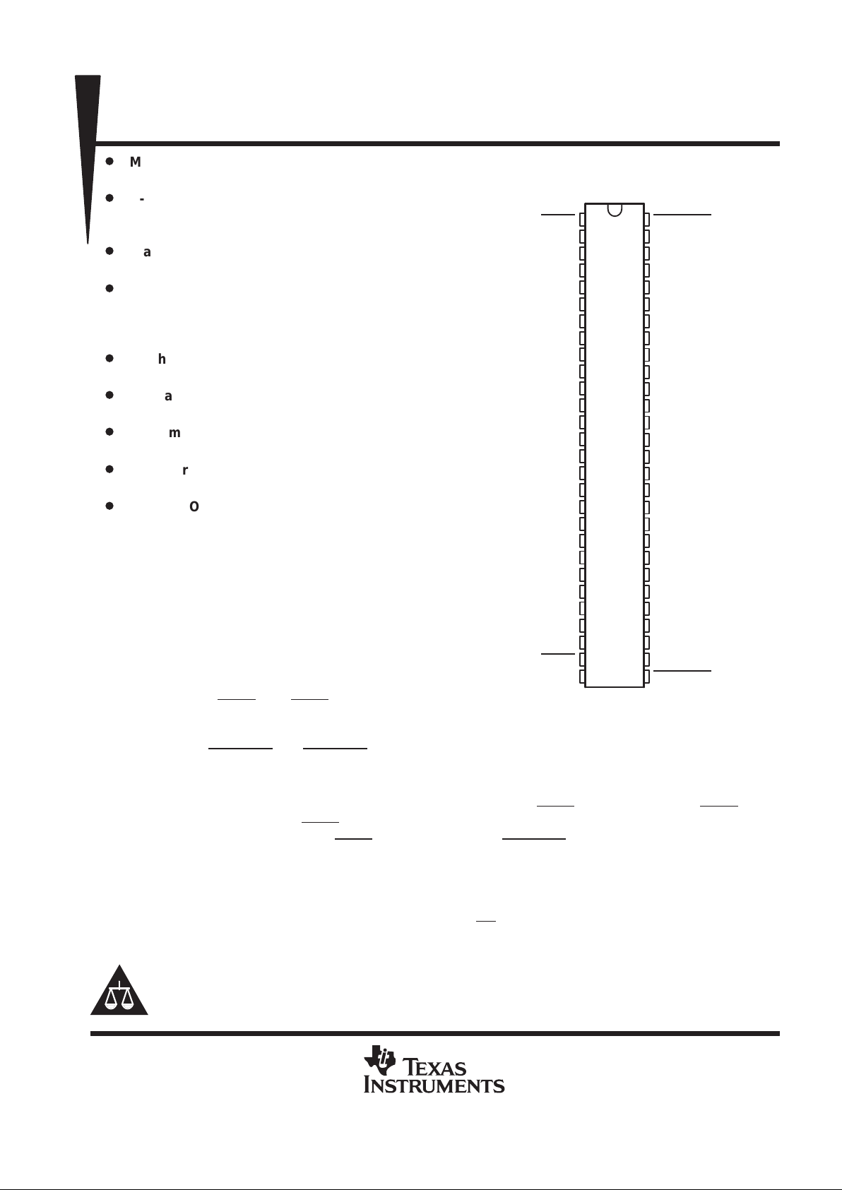
SN54ABT162601 . . . WD PACKAGE
SN74ABT162601 . . . DGG OR DL PACKAGE
(TOP VIEW)
1
2
3
4
5
6
7
8
9
10
11
12
13
14
15
16
17
18
19
20
21
22
23
24
25
26
27
28
56
55
54
53
52
51
50
49
48
47
46
45
44
43
42
41
40
39
38
37
36
35
34
33
32
31
30
29
OEAB
LEAB
A1
GND
A2
A3
V
CC
A4
A5
A6
GND
A7
A8
A9
A10
A11
A12
GND
A13
A14
A15
V
CC
A16
A17
GND
A18
OEBA
LEBA
CLKENAB
CLKAB
B1
GND
B2
B3
V
CC
B4
B5
B6
GND
B7
B8
B9
B10
B11
B12
GND
B13
B14
B15
V
CC
B16
B17
GND
B18
CLKBA
CLKENBA
On products compliant to MIL-PRF-38535, all parameters are tested
unless otherwise noted. On all other products, production
processing does not necessarily include testing of all parameters.
SN54ABT162601, SN74ABT162601
18-BIT UNIVERSAL BUS TRANSCEIVERS
WITH 3-STATE OUTPUTS
SCBS247G – AUGUST 1992 – REVISED JUL Y 1998
2
POST OFFICE BOX 655303 • DALLAS, TEXAS 75265
description (continued)
The SN54ABT162601 is characterized for operation over the full military temperature range of –55°C to 125°C.
The SN74ABT162601 is characterized for operation from –40°C to 85°C.
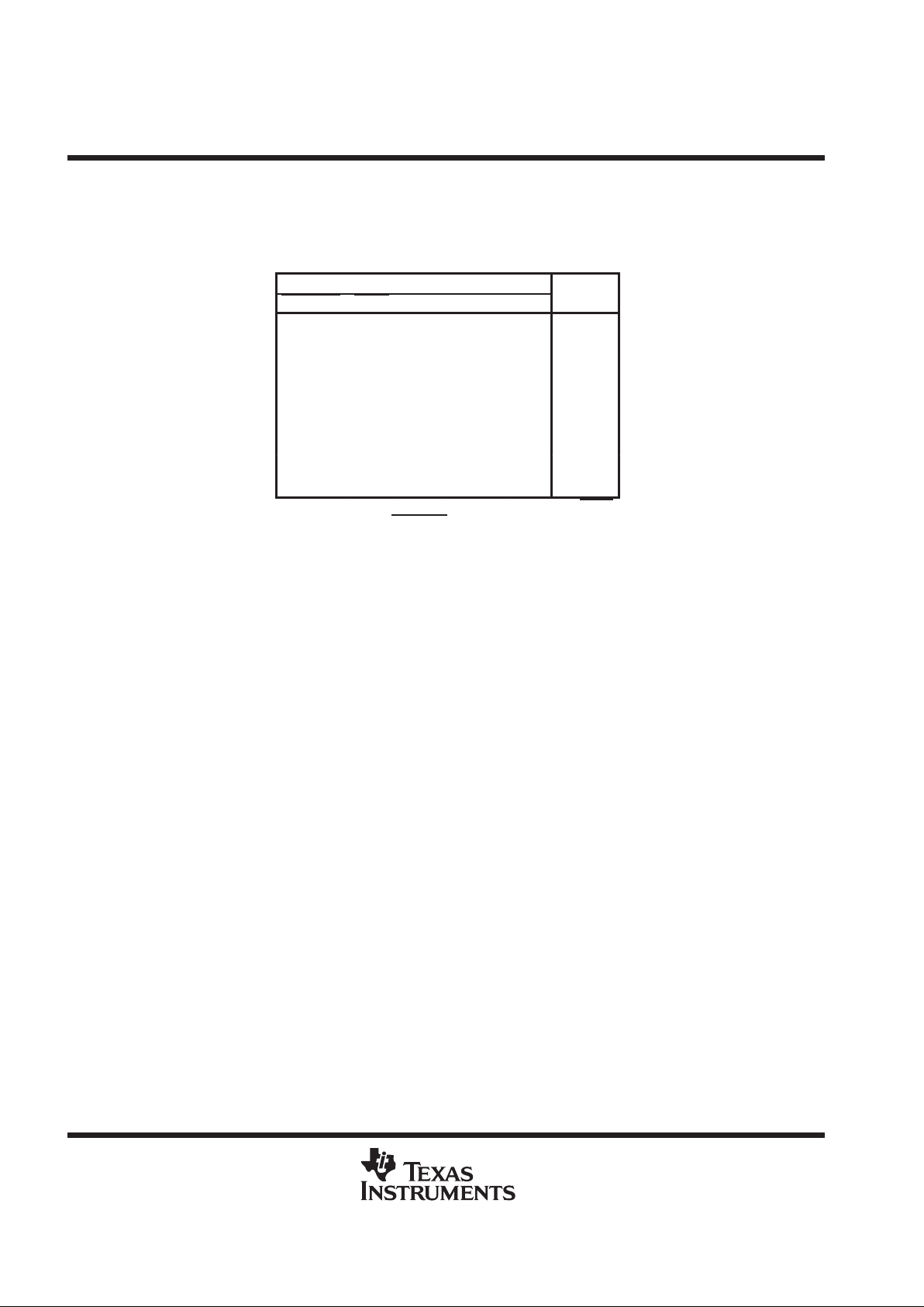
FUNCTION TABLE
†
INPUTS
OUTPUT
CLKENAB OEAB LEAB CLKAB A
B
X H X X X Z
X LH X L L
X LH XH H
H LL XXB
0
‡
H LL XXB
0
‡
L LL ↑ LL
L LL ↑ HH
L LL LXB
0
‡
L L L H X B
0
§
†
A-to-B data flow is shown: B-to-A flow is similar but uses OEBA,
LEBA, CLKBA, and CLKENBA
.
‡
Output level before the indicated steady-state input conditions
were established
§
Output level before the indicated steady-state input conditions
were established, provided that CLKAB was low before LEAB
went low
SN54ABT162601, SN74ABT162601
18-BIT UNIVERSAL BUS TRANSCEIVERS
WITH 3-STATE OUTPUTS
SCBS247G – AUGUST 1992 – REVISED JUL Y 1998
3
POST OFFICE BOX 655303 • DALLAS, TEXAS 75265
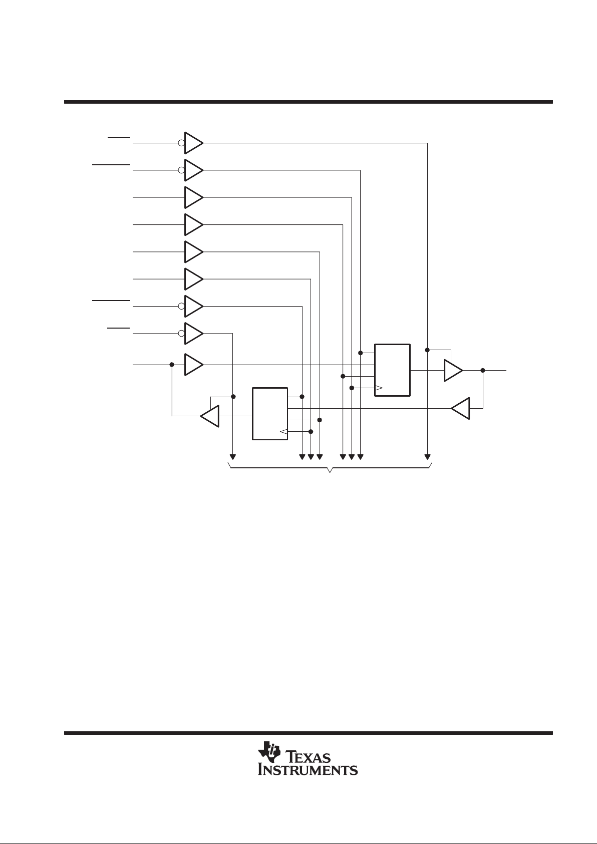
logic diagram (positive logic)
CE
1D
LE
CLK
CE
1D
LE
CLK
B1
OEAB
CLKENAB
CLKAB
LEAB
LEBA
CLKBA
CLKENBA
OEBA
A1
1
56
55
2
28
30
29
27
3
54
To 17 Other Channels
absolute maximum ratings over operating free-air temperature range (unless otherwise noted)
†
Supply voltage range, VCC –0.5 V to 7 V. . . . . . . . . . . . . . . . . . . . . . . . . . . . . . . . . . . . . . . . . . . . . . . . . . . . . . . . . .
Input voltage range, VI (except I/O ports) (see Note 1) –0.5 V to 7 V. . . . . . . . . . . . . . . . . . . . . . . . . . . . . . . . . .
Voltage range applied to any output in the high or power-off state, VO –0.5 V to 5.5 V. . . . . . . . . . . . . . . . . . .
Current into any output in the low state, IO: SN54ABT162601 (A port) 96 mA. . . . . . . . . . . . . . . . . . . . . . . . . .
SN74ABT162601 (A port) 128 mA. . . . . . . . . . . . . . . . . . . . . . . . .
B port 30 mA. . . . . . . . . . . . . . . . . . . . . . . . . . . . . . . . . . . . . . . . . . . .
Input clamp current, I
IK
(V
I
< 0) –18 mA. . . . . . . . . . . . . . . . . . . . . . . . . . . . . . . . . . . . . . . . . . . . . . . . . . . . . . . . . . .
Output clamp current, I
OK
(V
O
< 0) –50 mA. . . . . . . . . . . . . . . . . . . . . . . . . . . . . . . . . . . . . . . . . . . . . . . . . . . . . . . .
Package thermal impedance, θ
JA
(see Note 2): DGG package 81°C/W. . . . . . . . . . . . . . . . . . . . . . . . . . . . . . . .
DL package 74°C/W. . . . . . . . . . . . . . . . . . . . . . . . . . . . . . . . .
Storage temperature range, T
stg
–65°C to 150°C. . . . . . . . . . . . . . . . . . . . . . . . . . . . . . . . . . . . . . . . . . . . . . . . . . .
†
Stresses beyond those listed under “absolute maximum ratings” may cause permanent damage to the device. These are stress ratings only, and
functional operation of the device at these or any other conditions beyond those indicated under “recommended operating conditions” is not
implied. Exposure to absolute-maximum-rated conditions for extended periods may affect device reliability.
NOTES: 1. The input and output negative-voltage ratings may be exceeded if the input and output clamp-current ratings are observed.
2. The package thermal impedance is calculated in accordance with JESD 51.
 Loading...