

Texas Instruments SN74ABT162501DGGR, SN74ABT162501DL, SN74ABT162501DLR Datasheet
SN54ABT162501, SN74ABT162501
18-BIT UNIVERSAL BUS TRANSCEIVERS
WITH 3-STATE OUTPUTS
SCBS243E – SEPTEMBER 1992 – REVISED FEBRUARY 1999
1
POST OFFICE BOX 655303 • DALLAS, TEXAS 75265
D
Members of the Texas Instruments
Widebus
Family
D
B-Port Outputs Have Equivalent 25-Ω
Series Resistors, So No External Resistors
Are Required
D
State-of-the-Art
EPIC-ΙΙB
BiCMOS Design
Significantly Reduces Power Dissipation
D
UBT
(Universal Bus Transceiver)
Combines D-Type Latches and D-Type
Flip-Flops for Operation in Transparent,
Latched, or Clocked Mode
D
T ypical V
OLP
(Output Ground Bounce)
< 0.8 V at V
CC
= 5 V, TA = 25°C
D
High-Impedance State During Power Up
and Power Down
D
Flow-Through Architecture Optimizes PCB
Layout
D
Latch-Up Performance Exceeds 500 mA
Per JESD 17
D
ESD Protection Exceeds 2000 V Per
MIL-STD-883, Method 3015; Exceeds 200 V
Using Machine Model (C = 200 pF, R = 0)
D
Package Options Include Plastic Shrink
Small-Outline (DL) and Thin Shrink
Small-Outline (DGG) Packages and 380-mil
Fine-Pitch Ceramic Flat (WD) Package
Using 25-mil Center-to-Center Spacings
description
These 18-bit universal bus transceivers consist of
storage elements that can operate either as
D-type latches or D-type flip-flops to allow data
flow in transparent or clocked modes.
Data flow in each direction is controlled by output-enable (OEAB and OEBA
), latch-enable (LEAB and LEBA),
and clock (CLKAB and CLKBA) inputs. For A-to-B data flow, the device operates in the transparent mode when
LEAB is high. When LEAB is low, the A data is latched if CLKAB is held at a high or low logic level. If LEAB is
low, the A data is stored in the latch/flip-flop on the low-to-high transition of CLKAB. When OEAB is high, the
outputs are active. When OEAB is low, the outputs are in the high-impedance state.
Data flow for B to A is similar to that of A to B but uses OEBA
, LEBA, and CLKBA. The output enables are
complementary (OEAB is active high and OEBA
is active low).
The B-port outputs, which are designed to source or sink up to 12 mA, include equivalent 25-Ω series resistors
to reduce overshoot and undershoot.
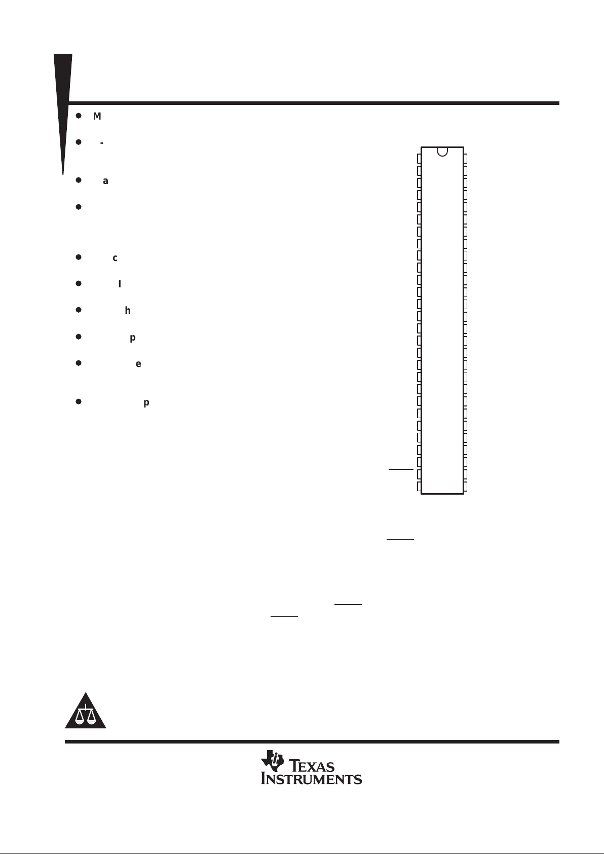
SN54ABT162501 ...WD PACKAGE
SN74ABT162501 . . . DGG OR DL PACKAGE
(TOP VIEW)
1
2
3
4
5
6
7
8
9
10
11
12
13
14
15
16
17
18
19
20
21
22
23
24
25
26
27
28
56
55
54
53
52
51
50
49
48
47
46
45
44
43
42
41
40
39
38
37
36
35
34
33
32
31
30
29
OEAB
LEAB
A1
GND
A2
A3
V
CC
A4
A5
A6
GND
A7
A8
A9
A10
A1 1
A12
GND
A13
A14
A15
V
CC
A16
A17
GND
A18
OEBA
LEBA
GND
CLKAB
B1
GND
B2
B3
V
CC
B4
B5
B6
GND
B7
B8
B9
B10
B1 1
B12
GND
B13
B14
B15
V
CC
B16
B17
GND
B18
CLKBA
GND
Copyright 1999, Texas Instruments Incorporated
UNLESS OTHERWISE NOTED this document contains PRODUCTION
DATA information current as of publication date. Products conform to
specifications per the terms of Texas Instruments standard warranty.
Production processing does not necessarily include testing of all
parameters.
Widebus, EPIC-ΙΙB, and UBT are trademarks of Texas Instruments Incorporated.
Please be aware that an important notice concerning availability, standard warranty, and use in critical applications of
Texas Instruments semiconductor products and disclaimers thereto appears at the end of this data sheet.
SN54ABT162501, SN74ABT162501
18-BIT UNIVERSAL BUS TRANSCEIVERS
WITH 3-STATE OUTPUTS
SCBS243E – SEPTEMBER 1992 – REVISED FEBRUARY 1999
2
POST OFFICE BOX 655303 • DALLAS, TEXAS 75265
description (continued)
When VCC is between 0 and 2.1 V , the device is in the high-impedance state during power up or power down.
However, to ensure the high-impedance state above 2.1 V, OE
should be tied to VCC through a pullup resistor
and OE should be tied to GND through a pulldown resistor; the minimum value of the resistor is determined by
the current-sinking/current-sourcing capability of the driver.
The SN54ABT162501 is characterized for operation over the full military temperature range of –55°C to 125°C.
The SN74ABT162501 is characterized for operation from –40°C to 85°C.
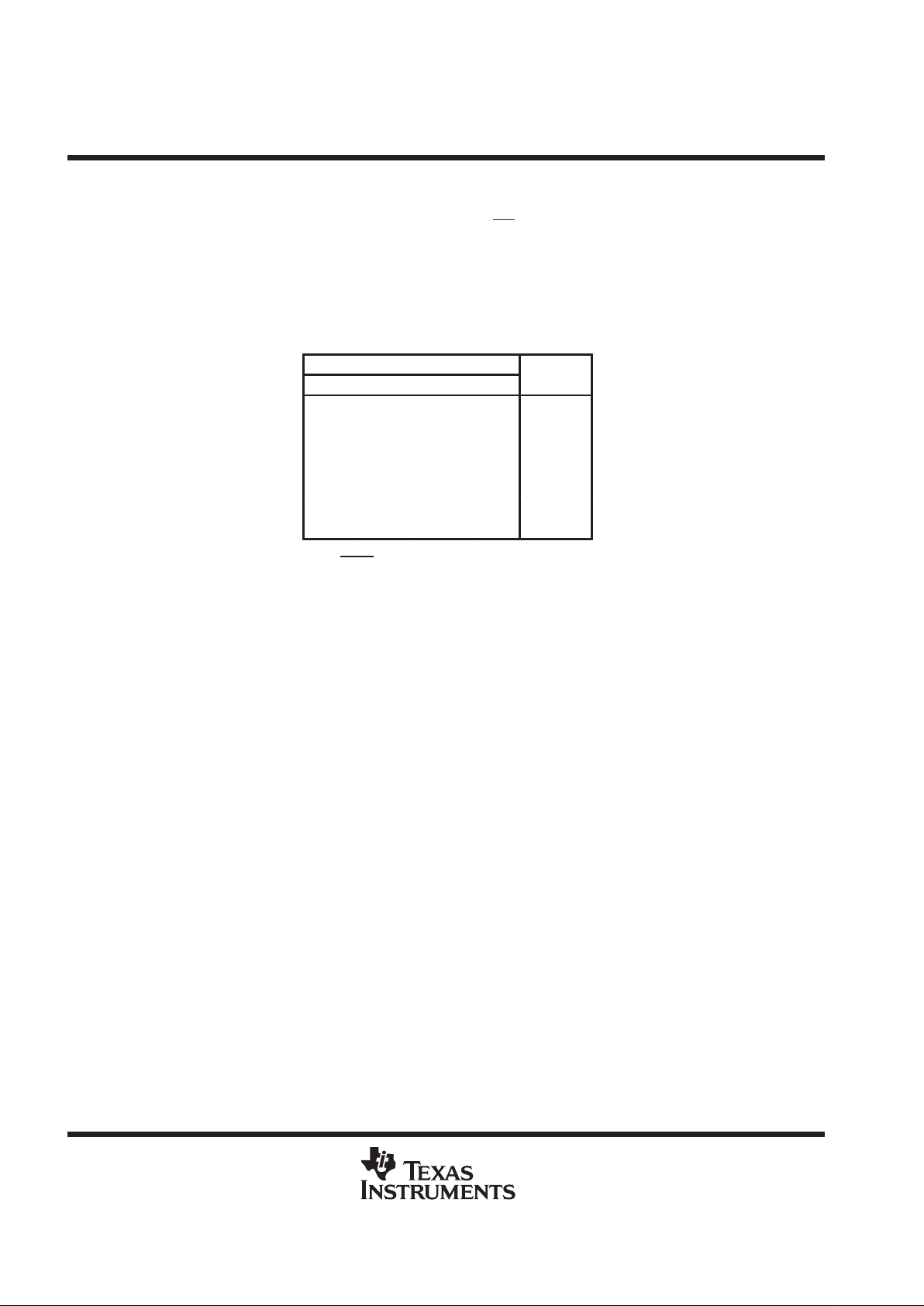
FUNCTION TABLE
†
INPUTS
OUTPUT
OEAB LEAB CLKAB A
B
L X X X Z
H HXLL
HHXHH
HL↑LL
HL↑HH
HLHXB
0
‡
HLLXB
0
§
†
A-to-B data flow is shown: B-to-A flow is similar but
uses OEBA
, LEBA, and CLKBA.
‡
Output level before the indicated steady-state input
conditions were established, provided that CLKAB
was high before LEAB went low
§
Output level before the indicated steady-state input
conditions were established
SN54ABT162501, SN74ABT162501
18-BIT UNIVERSAL BUS TRANSCEIVERS
WITH 3-STATE OUTPUTS
SCBS243E – SEPTEMBER 1992 – REVISED FEBRUARY 1999
3
POST OFFICE BOX 655303 • DALLAS, TEXAS 75265
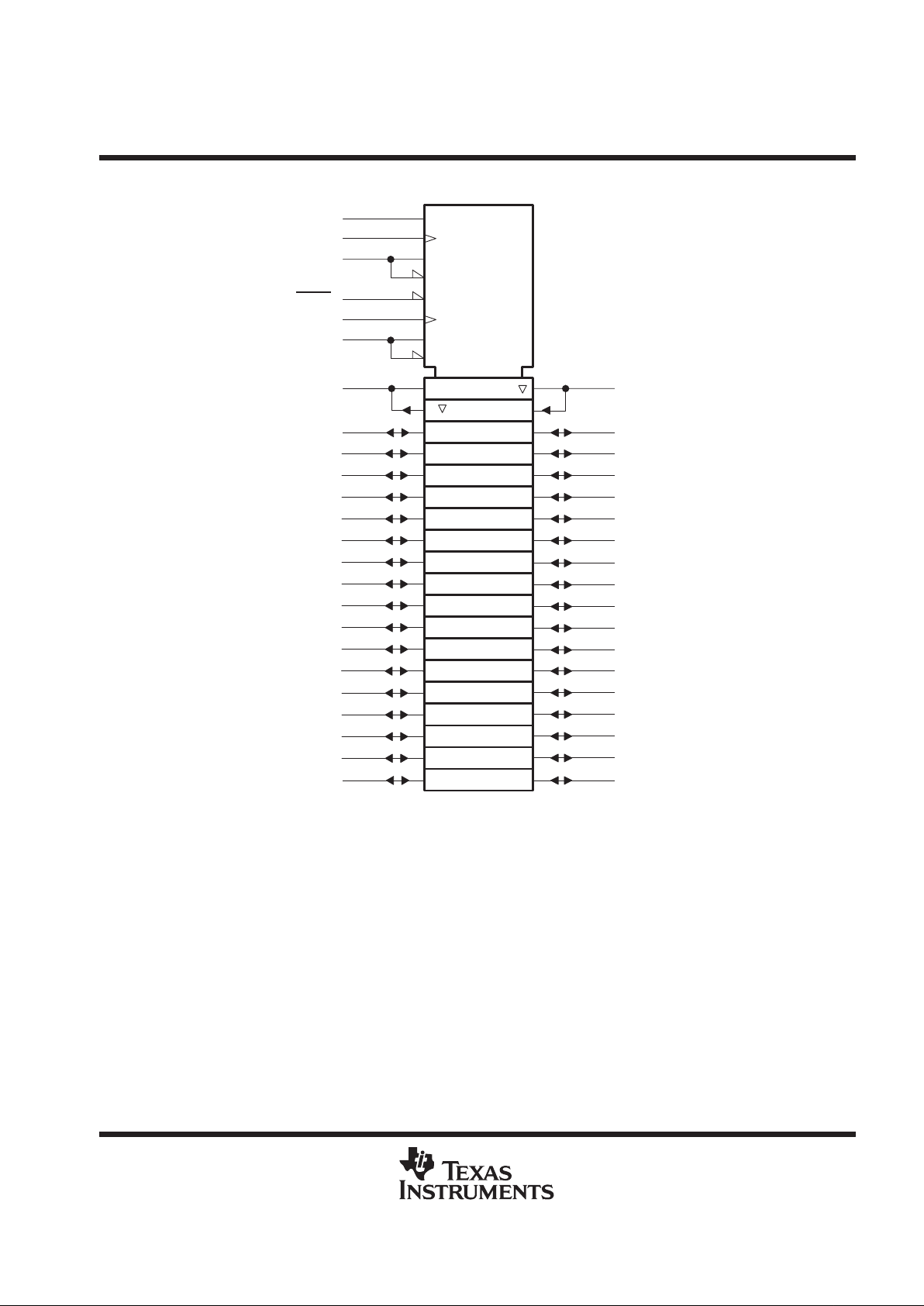
logic symbol
†
†
This symbol is in accordance with ANSI/IEEE Std 91-1984 and IEC Publication 617-12.
A2
5
EN1
1
OEAB
2C3
3D
3
A1 B1
54
A14
20
A15
21
A16
23
A17
24
A8
13
A9
14
A10
15
A11
16
A12
17
A3
6
A4
8
A5
9
A6
10
A7
12
B13
38
B14
37
B15
36
B16
34
B17
33
B18
31
6D
4
A18
26
B8
44
B9
43
B10
42
B11
41
B12
40
B3
51
B4
49
B5
48
B6
47
B7
45
B2
52
C6
28
LEBA
G5
30
CLKBA
EN4
27
C3
2
LEAB
G2
55
CLKAB
5C6
OEBA
11
1
A13
19
 Loading...