

Texas Instruments SN74ABT16241ADL, SN74ABT16241ADLR, SN74ABT16241ADGGR, SN74ABT16241ADGVR, SNJ54ABT16241AWD Datasheet
SN54ABT16241A, SN74ABT16241A
16-BIT BUFFERS/DRIVERS
WITH 3-STATE OUTPUTS
SCBS096G – FEBRUARY 1991 – REVISED OCTOBER 1998
1
POST OFFICE BOX 655303 • DALLAS, TEXAS 75265
D
Members of the Texas Instruments
Widebus
Family
D
State-of-the-Art
EPIC-ΙΙB
BiCMOS Design
Significantly Reduces Power Dissipation
D
T ypical V
OLP
(Output Ground Bounce) < 1 V
at V
CC
= 5 V, TA = 25°C
D
Distributed VCC and GND Pin Configuration
Minimizes High-Speed Switching Noise
D
Flow-Through Architecture Optimizes PCB
Layout
D
High-Drive Outputs (–32-mA IOH, 64-mA IOL)
D
Latch-Up Performance Exceeds 500 mA
Per JESD 17
D
ESD Protection Exceeds 2000 V Per
MIL-STD-883, Method 3015; Exceeds 200 V
Using Machine Model (C = 200 pF, R = 0)
D
Package Options Include Plastic 300-mil
Shrink Small-Outline (DL), Thin Shrink
Small-Outline (DGG), and Thin Very
Small-Outline (DGV) Packages and 380-mil
Fine-Pitch Ceramic Flat (WD) Package
Using 25-mil Center-to-Center Spacings
description
The ’ABT16241A devices are 16-bit buffers and
line drivers designed specifically to improve both
the performance and density of 3-state memory
address drivers, clock drivers, and bus-oriented
receivers and transmitters.
These devices can be used as four 4-bit buffers, two 8-bit buffers, or one 16-bit buffer. These devices provide
true outputs and complementary output-enable (OE and OE
) inputs.
T o ensure the high-impedance state during power up or power down, OE
should be tied to V
CC
through a pullup
resistor; the minimum value of the resistor is determined by the current-sinking capability of the driver. OE
should be tied to GND through a pulldown resistor; the minimum value of the resistor is determined by the
current-sourcing capability of the driver.
The SN54ABT16241A is characterized for operation over the full military temperature range of –55°C to 125°C.
The SN74ABT16241A is characterized for operation from –40°C to 85°C.
Copyright 1998, Texas Instruments Incorporated
PRODUCTION DATA information is current as of publication date.
Products conform to specifications per the terms of Texas Instruments
standard warranty. Production processing does not necessarily include
testing of all parameters.
Please be aware that an important notice concerning availability, standard warranty, and use in critical applications of
Texas Instruments semiconductor products and disclaimers thereto appears at the end of this data sheet.
Widebus and EPIC-ΙΙB are trademarks of Texas Instruments Incorporated.
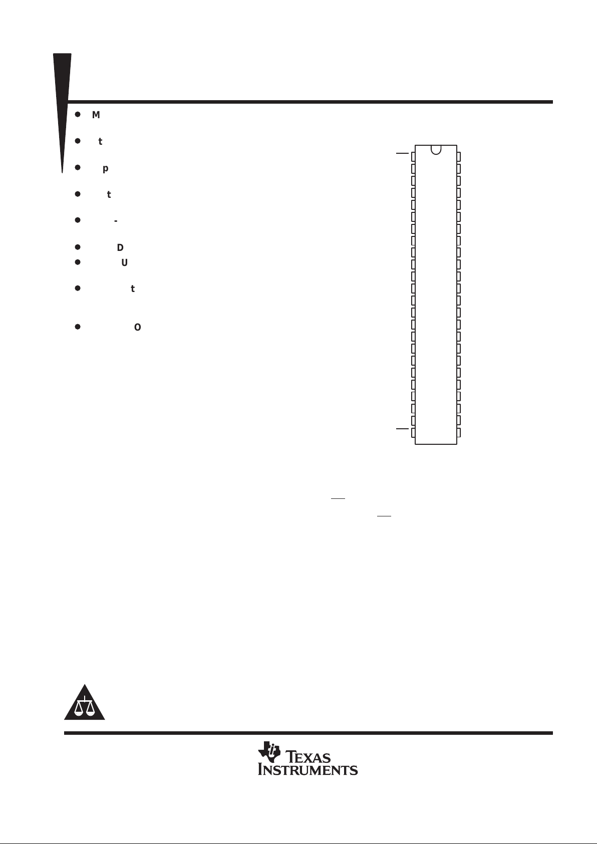
SN54ABT16241A . . . WD PACKAGE
SN74ABT16241A . . . DGG, DGV, OR DL PACKAGE
(TOP VIEW)
1
2
3
4
5
6
7
8
9
10
11
12
13
14
15
16
17
18
19
20
21
22
23
24
48
47
46
45
44
43
42
41
40
39
38
37
36
35
34
33
32
31
30
29
28
27
26
25
1OE
1Y1
1Y2
GND
1Y3
1Y4
V
CC
2Y1
2Y2
GND
2Y3
2Y4
3Y1
3Y2
GND
3Y3
3Y4
V
CC
4Y1
4Y2
GND
4Y3
4Y4
4OE
2OE
1A1
1A2
GND
1A3
1A4
V
CC
2A1
2A2
GND
2A3
2A4
3A1
3A2
GND
3A3
3A4
V
CC
4A1
4A2
GND
4A3
4A4
3OE
On products compliant to MIL-PRF-38535, all parameters are tested
unless otherwise noted. On all other products, production
processing does not necessarily include testing of all parameters.
SN54ABT16241A, SN74ABT16241A
16-BIT BUFFERS/DRIVERS
WITH 3-STATE OUTPUTS
SCBS096G – FEBRUARY 1991 – REVISED OCTOBER 1998
2
POST OFFICE BOX 655303 • DALLAS, TEXAS 75265
FUNCTION TABLES
INPUTS
OUTPUTS
1OE, 4OE 1A, 4A
1Y, 4Y
L H H
L LL
HXZ
INPUTS
OUTPUTS
2OE, 3OE 2A, 3A
2Y, 3Y
H H H
H LL
LXZ
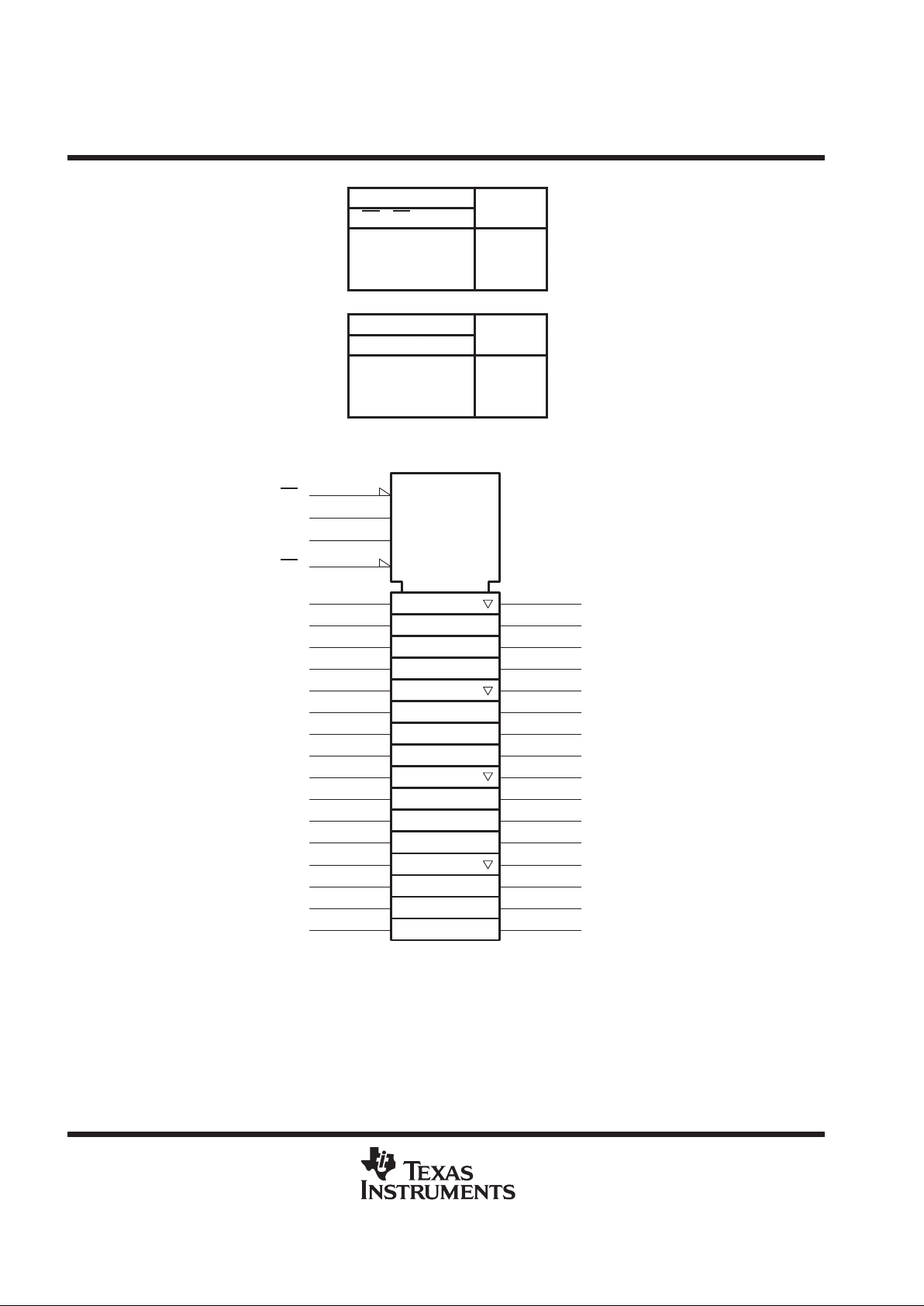
logic symbol
†
47
1A1
46
1A2
44
1A3
43
1A4
1Y1
2
1Y2
3
1Y3
5
1Y4
6
41
2A1
40
2A2
38
2A3
37
2A4
2Y1
8
2Y2
9
2Y3
11
2Y4
12
36
3A1
35
3A2
33
3A3
32
3A4
3Y1
13
3Y2
14
3Y3
16
3Y4
17
30
4A1
29
4A2
27
4A3
26
4A4
4Y1
19
4Y2
20
4Y3
22
4Y4
23
EN1
1
EN2
48
2OE
EN3
25
3OE
EN4
24
1OE
4OE
†
This symbol is in accordance with ANSI/IEEE Std 91-1984 and IEC Publication 617-12.
1
1
1
1
1
2
3
4
SN54ABT16241A, SN74ABT16241A
16-BIT BUFFERS/DRIVERS
WITH 3-STATE OUTPUTS
SCBS096G – FEBRUARY 1991 – REVISED OCTOBER 1998
3
POST OFFICE BOX 655303 • DALLAS, TEXAS 75265
logic diagram (positive logic)
1OE
1A1
1A2
1A3
1A4
1Y1
1Y2
1Y3
1Y4
1
47
46
44
43
2
3
5
6
2OE
2A1
2A2
2A3
2A4
2Y1
2Y2
2Y3
2Y4
48
41
40
38
37
8
9
11
12
3OE
3A1
3A2
3A3
3A4
3Y1
3Y2
3Y3
3Y4
25
36
35
33
32
13
14
16
17
4OE
4A1
4A2
4A3
4A4
4Y1
4Y2
4Y3
4Y4
24
30
29
27
26
19
20
22
23
absolute maximum ratings over operating free-air temperature range (unless otherwise noted)
†
Supply voltage range, V
CC
–0.5 V to 7 V. . . . . . . . . . . . . . . . . . . . . . . . . . . . . . . . . . . . . . . . . . . . . . . . . . . . . . . . . .
Input voltage range, V
I
(see Note 1) –0.5 V to 7 V. . . . . . . . . . . . . . . . . . . . . . . . . . . . . . . . . . . . . . . . . . . . . . . . . .
Voltage range applied to any output in the high or power-off state, V
O
–0.5 V to 5.5 V. . . . . . . . . . . . . . . . . . .
Current into any output in the low state, I
O
: SN54ABT16241A 96 mA. . . . . . . . . . . . . . . . . . . . . . . . . . . . . . . . .
SN74ABT16241A 128 mA. . . . . . . . . . . . . . . . . . . . . . . . . . . . . . . .
Input clamp current, I
IK
(VI < 0) –18 mA. . . . . . . . . . . . . . . . . . . . . . . . . . . . . . . . . . . . . . . . . . . . . . . . . . . . . . . . . . .
Output clamp current, I
OK
(VO < 0) –50 mA. . . . . . . . . . . . . . . . . . . . . . . . . . . . . . . . . . . . . . . . . . . . . . . . . . . . . . . .
Package thermal impedance, θ
JA
(see Note 2): DGG package 89°C/W. . . . . . . . . . . . . . . . . . . . . . . . . . . . . . .
DGV package 93°C/W. . . . . . . . . . . . . . . . . . . . . . . . . . . . . . . .
DL package 94°C/W. . . . . . . . . . . . . . . . . . . . . . . . . . . . . . . . .
Storage temperature range, T
stg
–65°C to 150°C. . . . . . . . . . . . . . . . . . . . . . . . . . . . . . . . . . . . . . . . . . . . . . . . . . .
†
Stresses beyond those listed under “absolute maximum ratings” may cause permanent damage to the device. These are stress ratings only, and
functional operation of the device at these or any other conditions beyond those indicated under “recommended operating conditions” is not
implied. Exposure to absolute-maximum-rated conditions for extended periods may affect device reliability.
NOTES: 1. The input and output negative-voltage ratings may be exceeded if the input and output clamp-current ratings are observed.
2. The package thermal impedance is calculated in accordance with JESD 51.
 Loading...