

Texas Instruments SN74ABT126D, SN74ABT126DBLE, SN74ABT126DBR, SN74ABT126DR, SN74ABT126N Datasheet
...
SN54ABT126, SN74ABT126
QUADRUPLE BUS BUFFER GATES
WITH 3-STATE OUTPUTS
SCBS183D – FEBRUARY 1991 – REVISED JANUARY 1999
D
State-of-the-Art
EPIC-ΙΙB
BiCMOS Design
Significantly Reduces Power Dissipation
D
Typical V
at V
D
High-Impedance State During Power Up
= 5 V, TA = 25°C
CC
(Output Ground Bounce) <1 V
OLP
and Power Down
D
High-Drive Outputs (–32-mA IOH, 64-mA IOL)
D
Latch-Up Performance Exceeds 500 mA Per
JESD 17
D
ESD Protection Exceeds 2000 V Per
MIL-STD-883, Method 3015; Exceeds 200 V
Using Machine Model (C = 200 pF, R = 0)
D
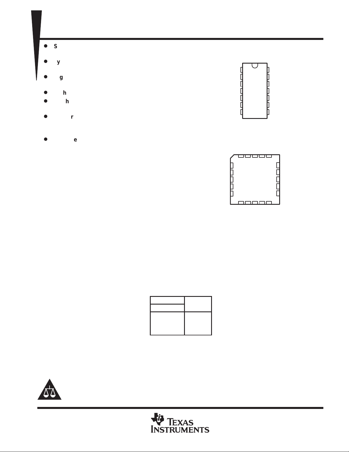
Package Options Include Plastic
Small-Outline (D) and Shrink Small-Outline
(DB) Packages, Ceramic Chip Carriers (FK),
and Plastic (N) and Ceramic (J) DIPs
description
The ’ABT126 bus buffer gates feature
independent line drivers with 3-state outputs.
Each output is disabled when the associated
output-enable (OE) input is low.
When V
in the high-impedance state during power up or
power down. However, to ensure the
high-impedance state above 2.1 V , OE should be
tied to GND through a pulldown resistor; the
minimum value of the resistor is determined by the
current-sourcing capability of the driver.
is between 0 and 2.1 V, the device is
CC
SN54ABT126 ...J PACKAGE
SN74ABT126 . . . D, DB, OR N PACKAGE
SN54ABT126 . . . FK PACKAGE
1Y
NC
2OE
NC
2A
NC – No internal connection
(TOP VIEW)
1OE
2OE
GND
1
1A
2
1Y
3
4
2A
5
2Y
6
7
(TOP VIEW)
1A
3212019
4
5
6
7
8
910111213
2Y
1OE
GND
14
13
12
11
10
NC
NC
9
8
CC
V
3Y
V
CC
4OE
4A
4Y
3OE
3A
3Y
4OE
18
17
16
15
14
3A
4A
NC
4Y
NC
3OE
The SN54ABT126 is characterized for operation over the full military temperature range of –55°C to 125°C.
The SN74ABT126 is characterized for operation from –40°C to 85°C.
FUNCTION TABLE
(each buffer)
Please be aware that an important notice concerning availability, standard warranty, and use in critical applications of
Texas Instruments semiconductor products and disclaimers thereto appears at the end of this data sheet.
EPIC-ΙΙB is a trademark of Texas Instruments Incorporated.
UNLESS OTHERWISE NOTED this document contains PRODUCTION
DATA information current as of publication date. Products conform to
specifications per the terms of Texas Instruments standard warranty.
Production processing does not necessarily include testing of all
parameters.
INPUTS
OE A
H H H
H LL
LXZ
OUTPUT
Y
Copyright 1999, Texas Instruments Incorporated
POST OFFICE BOX 655303 • DALLAS, TEXAS 75265
1
SN54ABT126, SN74ABT126
QUADRUPLE BUS BUFFER GATES
WITH 3-STATE OUTPUTS
SCBS183D – FEBRUARY 1991 – REVISED JANUARY 1999
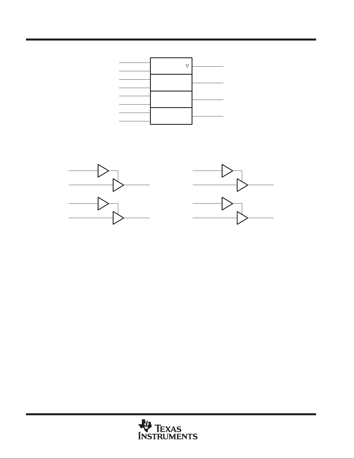
logic symbol
†
This symbol is in accordance with ANSI/IEEE Std 91-1984 and IEC Publication 617-12.
Pin numbers shown are for the D, DB, J, and N packages.
†
1OE
1A
2OE
2A
3OE
3A
4OE
4A
1
2
4
5
10
9
13
12
EN
1
logic diagram (positive logic)
1
1OE
2
1A 1Y
4
2OE
3
3OE
3A 3Y
4OE
10
9
13
3
1Y
6
2Y
8
3Y
11
4Y
8
5
2A 2Y
Pin numbers shown are for the D, DB, J, and N packages.
6
12
4A 4Y
11
absolute maximum ratings over operating free-air temperature range (unless otherwise noted)
Supply voltage range, V
Input voltage range, V
Voltage range applied to any output in the high or power-off state, V
Current into any output in the low state, I
Input clamp current, I
Output clamp current, I
Package thermal impedance, θ
Storage temperature range, T
‡
Stresses beyond those listed under “absolute maximum ratings” may cause permanent damage to the device. These are stressratings only, and
functional operation of the device at these or any other conditions beyond those indicated under “recommended operating conditions” is not
implied. Exposure to absolute-maximum-rated conditions for extended periods may affect device reliability.
NOTES: 1. The input and output negative-voltage ratings may be exceeded if the input and output clamp-current ratings are observed.
2. The package thermal impedance is calculated in accordance with JESD 51, except for through-hole packages, which use a trace
length of zero.
–0.5 V to 7 V. . . . . . . . . . . . . . . . . . . . . . . . . . . . . . . . . . . . . . . . . . . . . . . . . . . . . . . . . .
CC
(see Note 1) –0.5 V to 7 V. . . . . . . . . . . . . . . . . . . . . . . . . . . . . . . . . . . . . . . . . . . . . . . . . .
I
: SN54ABT126 96 mA. . . . . . . . . . . . . . . . . . . . . . . . . . . . . . . . . . . .
O
–0.5 V to 5.5 V. . . . . . . . . . . . . . . . . . .
O
SN74ABT126 128 mA. . . . . . . . . . . . . . . . . . . . . . . . . . . . . . . . . . .
(VI < 0) –18 mA. . . . . . . . . . . . . . . . . . . . . . . . . . . . . . . . . . . . . . . . . . . . . . . . . . . . . . . . . . .
IK
(VO < 0) –50 mA. . . . . . . . . . . . . . . . . . . . . . . . . . . . . . . . . . . . . . . . . . . . . . . . . . . . . . . .
OK
(see Note 2): D package 127°C/W. . . . . . . . . . . . . . . . . . . . . . . . . . . . . . . . . .
JA
DB package 158°C/W. . . . . . . . . . . . . . . . . . . . . . . . . . . . . . . .
N package 78°C/W. . . . . . . . . . . . . . . . . . . . . . . . . . . . . . . . . . .
–65°C to 150°C. . . . . . . . . . . . . . . . . . . . . . . . . . . . . . . . . . . . . . . . . . . . . . . . . . .
stg
‡
2
POST OFFICE BOX 655303 • DALLAS, TEXAS 75265
 Loading...