

SN64BCT244
OCTAL BUFFER/DRIVER
WITH 3-STATE OUTPUTS
SCBS027A – FEBRUARY 1989 – REVISED JANUAR Y 1994
Copyright 1994, Texas Instruments Incorporated
3–1
POST OFFICE BOX 655303 • DALLAS, TEXAS 75265
• State-of-the-Art BiCMOS Design
Significantly Reduces I
CCZ
• 3-State Outputs Drive Bus Lines or
Buffer-Memory Address Registers
• P-N-P Inputs Reduce DC Loading
• High-Impedance State During Power Up
and Power Down
• Package Options Include Plastic
Small-Outline (DW) Packages and Standard
Plastic 300-mil DIPs (N)
description
This octal buffer and line driver is designed
specifically to improve both the performance and
density of 3-state memory address drivers, clock drivers, and bus-oriented receivers and transmitters. Taken
together with the SN64BCT240 and SN64BCT241, these devices provide the choice of selected combinations
of inverting and noninverting outputs, symmetrical active-low output-enable (OE
) inputs, and complementary
OE and OE inputs.
The SN64BCT244 is organized as two 4-bit buffers/line drivers with separate output-enable (OE) inputs. When
OE is low, the device passes data from the A inputs to the Y outputs. When OE is high, the outputs are in the
high-impedance state.
The outputs are in a high-impedance state during power up and power down while the supply voltage is less
than approximately 3 V.
The SN64BCT244 is characterized for operation from –40°C to 85°C.
FUNCTION TABLE
(each buffer)
INPUTS
OUTPUT
OE A
Y
L H H
L LL
H X Z
1
2
3
4
5
6
7
8
9
10
20
19
18
17
16
15
14
13
12
11
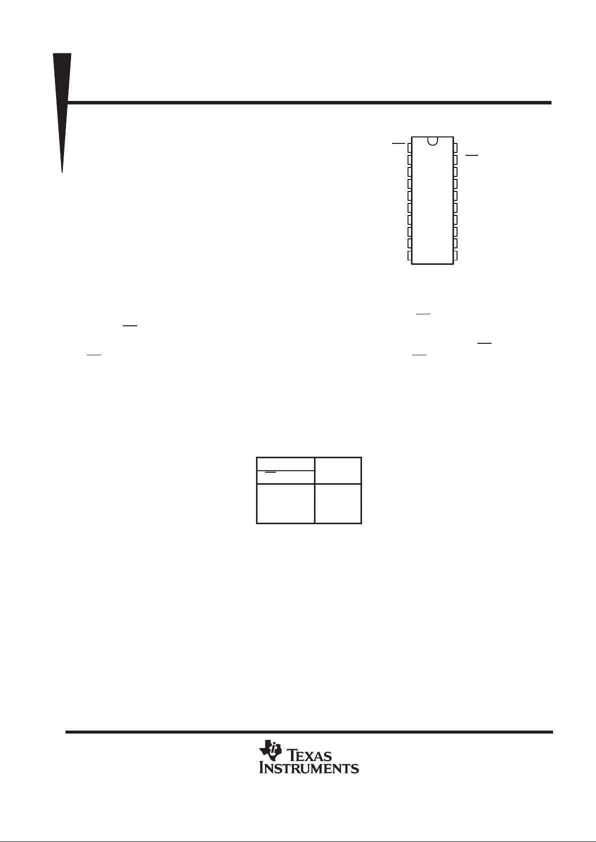
1OE
1A1
2Y4
1A2
2Y3
1A3
2Y2
1A4
2Y1
GND
V
CC
2OE
1Y1
2A4
1Y2
2A3
1Y3
2A2
1Y4
2A1
DW OR N PACKAGE
(TOP VIEW)
PRODUCTION DATA information is current as of publication date.
Products conform to specifications per the terms of Texas Instruments
standard warranty. Production processing does not necessarily include
testing of all parameters.
SN64BCT244
OCTAL BUFFER/DRIVER
WITH 3-STATE OUTPUTS
SCBS027A – FEBRUAR Y 1989 – REVISED JANUAR Y 1994
3–2
POST OFFICE BOX 655303 • DALLAS, TEXAS 75265
logic symbol
†
logic diagram (positive logic)
1
2
4
6
8
19
11
13
15
17 3
5
7
9
12
14
16
18
1A1
1A2
1A3
1A4
1Y1
2A1
2A2
2A3
2A4
2Y1
1Y2
1Y3
1Y4
2Y2
2Y3
2Y4
2OE
1OE
2
1A1
4
1A2
6
1A3
8
1A4
EN
1
1Y1
18
1Y2
16
1Y3
14
1Y4
12
11
2A1
13
2A2
15
2A3
17
2A4
EN
19
2Y1
9
2Y2
7
2Y3
5
2Y4
3
1OE
2OE
†
This symbol is in accordance with ANSI/IEEE Std 91-1984
and IEC Publication 617-12.
absolute maximum ratings over operating free-air temperature range (unless otherwise noted)
‡
Supply voltage range, V
CC
–0.5 V to 7 V. . . . . . . . . . . . . . . . . . . . . . . . . . . . . . . . . . . . . . . . . . . . . . . . . . . . . . . . . .
Input voltage range, VI (see Note 1) –0.5 V to 7 V. . . . . . . . . . . . . . . . . . . . . . . . . . . . . . . . . . . . . . . . . . . . . . . . . . .
Voltage range applied to any output in the disabled or power-off state, V
O
–0.5 V to 5.5 V. . . . . . . . . . . . . . . .
Voltage range applied to any output in the high state, V
O
–0.5 V to V
CC
. . . . . . . . . . . . . . . . . . . . . . . . . . . . . . .
Current into any output in the low state, I
O
128 mA. . . . . . . . . . . . . . . . . . . . . . . . . . . . . . . . . . . . . . . . . . . . . . . . . .
Operating free-air temperature range –40°C to 85°C. . . . . . . . . . . . . . . . . . . . . . . . . . . . . . . . . . . . . . . . . . . . . . . .
Storage temperature range –65°C to 150°C. . . . . . . . . . . . . . . . . . . . . . . . . . . . . . . . . . . . . . . . . . . . . . . . . . . . . . . .
‡
Stresses beyond those listed under “absolute maximum ratings” may cause permanent damage to the device. These are stress ratings only, and
functional operation of the device at these or any other conditions beyond those indicated under “recommended operating conditions” is not
implied. Exposure to absolute-maximum-rated conditions for extended periods may affect device reliability.
NOTE 1: The input negative voltage rating may be exceeded if the input clamp current rating is observed.
SN64BCT244
OCTAL BUFFER/DRIVER
WITH 3-STATE OUTPUTS
SCBS027A – FEBRUARY 1989 – REVISED JANUAR Y 1994
3–3
POST OFFICE BOX 655303 • DALLAS, TEXAS 75265
recommended operating conditions
MIN NOM MAX UNIT
V
CC
Supply voltage 4.5 5 5.5 V
V
IH
High-level input voltage 2 V
V
IL
Low-level input voltage 0.8 V
I
IK
Input clamp current –18 mA
I
OH
High-level output current –15 mA
I
OL
Low-level output current 64 mA
T
A
Operating free-air temperature –40 85 °C
electrical characteristics over recommended operating free-air temperature range (unless
otherwise noted)
PARAMETER TEST CONDITIONS MIN TYP†MAX UNIT
V
IK
VCC = 4.5 V, II = –18 mA –1.2 V
IOH = –3 mA 2.4 3.3
V
OH
V
CC
= 4.5
V
IOH = –15 mA 2 3.1
V
V
OL
VCC = 4.5 V, IOL = 64 mA 0.42 0.55 V
I
I
VCC = 5.5 V, VI = 7 V 0.1 mA
I
IH
VCC = 5.5 V, VI = 2.7 V 20 µA
I
IL
VCC = 5.5 V, VI = 0.5 V –1 mA
VCC = 0 to 2.3 V (power up)
"
50
I
OZ
VCC = 1.8 V to 0 (power down)
V
O
=
2.7 V or 0.5 V
,
OE at 0.8 V
"
50
µ
A
I
OZH
VCC = 5.5 V, VO = 2.7 V 50 µA
I
OZL
VCC = 5.5 V, VO = 0.5 V –50 µA
I
OS
†
VCC = 5.5 V, VO = 0 –100 –225 mA
I
CCH
VCC = 5.5 V, Output open 23 40 mA
I
CCL
VCC = 5.5 V, Output open 53 80 mA
I
CCZ
VCC = 5.5 V, Output open 4 10 mA
†
All typical values are at VCC = 5 V.
‡
Not more than one output should be tested at a time, and the duration of the test should not exceed one second.
switching characteristics (see Note 2)
PARAMETER
FROM
(INPUT)
TO
(OUTPUT)
VCC = 5 V,
CL = 50 pF,
R1 = 500 Ω,
R2 = 500 Ω,
TA = 25°C
VCC = 4.5 V to 5.5 V,
CL = 50 pF,
R1 = 500 Ω,
R2 = 500 Ω,
TA = MIN to MAX
§
UNIT
MIN TYP MAX MIN MAX
t
PLH
1.2 2.5 4.4 0.9 5.3
t
PHL
A
Y
1.7 3.2 5 1.4 6
ns
t
PZH
2 5.7 7.8 2 9
t
PZL
OE
Y
2 5.9 8.1 2 9.4
ns
t
PHZ
2 5.4 6.7 2 8
t
PLZ
OE
Y
2 6.1 7.6 2 9.8
ns
§
For conditions shown as MIN or MAX, use the appropriate value specified under recommended operating conditions.
NOTE 2: Load circuits and voltage waveforms are shown in Section 1.

SN64BCT244
OCTAL BUFFER/DRIVER
WITH 3-STATE OUTPUTS
SCBS027A – FEBRUAR Y 1989 – REVISED JANUAR Y 1994
3–4
POST OFFICE BOX 655303 • DALLAS, TEXAS 75265

IMPORTANT NOTICE
T exas Instruments and its subsidiaries (TI) reserve the right to make changes to their products or to discontinue
any product or service without notice, and advise customers to obtain the latest version of relevant information
to verify, before placing orders, that information being relied on is current and complete. All products are sold
subject to the terms and conditions of sale supplied at the time of order acknowledgement, including those
pertaining to warranty, patent infringement, and limitation of liability.
TI warrants performance of its semiconductor products to the specifications applicable at the time of sale in
accordance with TI’s standard warranty. Testing and other quality control techniques are utilized to the extent
TI deems necessary to support this warranty. Specific testing of all parameters of each device is not necessarily
performed, except those mandated by government requirements.
CERT AIN APPLICATIONS USING SEMICONDUCTOR PRODUCTS MAY INVOLVE POTENTIAL RISKS OF
DEATH, PERSONAL INJURY, OR SEVERE PROPERTY OR ENVIRONMENTAL DAMAGE (“CRITICAL
APPLICATIONS”). TI SEMICONDUCTOR PRODUCTS ARE NOT DESIGNED, AUTHORIZED, OR
WARRANTED TO BE SUITABLE FOR USE IN LIFE-SUPPORT DEVICES OR SYSTEMS OR OTHER
CRITICAL APPLICATIONS. INCLUSION OF TI PRODUCTS IN SUCH APPLICA TIONS IS UNDERSTOOD T O
BE FULLY AT THE CUSTOMER’S RISK.
In order to minimize risks associated with the customer’s applications, adequate design and operating
safeguards must be provided by the customer to minimize inherent or procedural hazards.
TI assumes no liability for applications assistance or customer product design. TI does not warrant or represent
that any license, either express or implied, is granted under any patent right, copyright, mask work right, or other
intellectual property right of TI covering or relating to any combination, machine, or process in which such
semiconductor products or services might be or are used. TI’s publication of information regarding any third
party’s products or services does not constitute TI’s approval, warranty or endorsement thereof.
Copyright 1998, Texas Instruments Incorporated
 Loading...