

SN64BCT125A
QUADRUPLE BUS BUFFER GATE
WITH 3-STATE OUTPUTS
SCBS052B – JULY 1990 – REVISED MAY 1994
Copyright 1994, Texas Instruments Incorporated
3–3
POST OFFICE BOX 655303 • DALLAS, TEXAS 75265
• State-of-the-Art BiCMOS Design
Significantly Reduces I
CCZ
• High-Impedance State During Power-Up
and Power-Down
• 3-State Outputs Drive Bus Lines or
Buffer-Memory Address Registers
• ESD Protection Exceeds 2000 V
Per MIL-STD-883C Method 3015
• Package Options Include Plastic
Small-Outline (D) Packages and Standard
Plastic 300-mil DIPs (N)
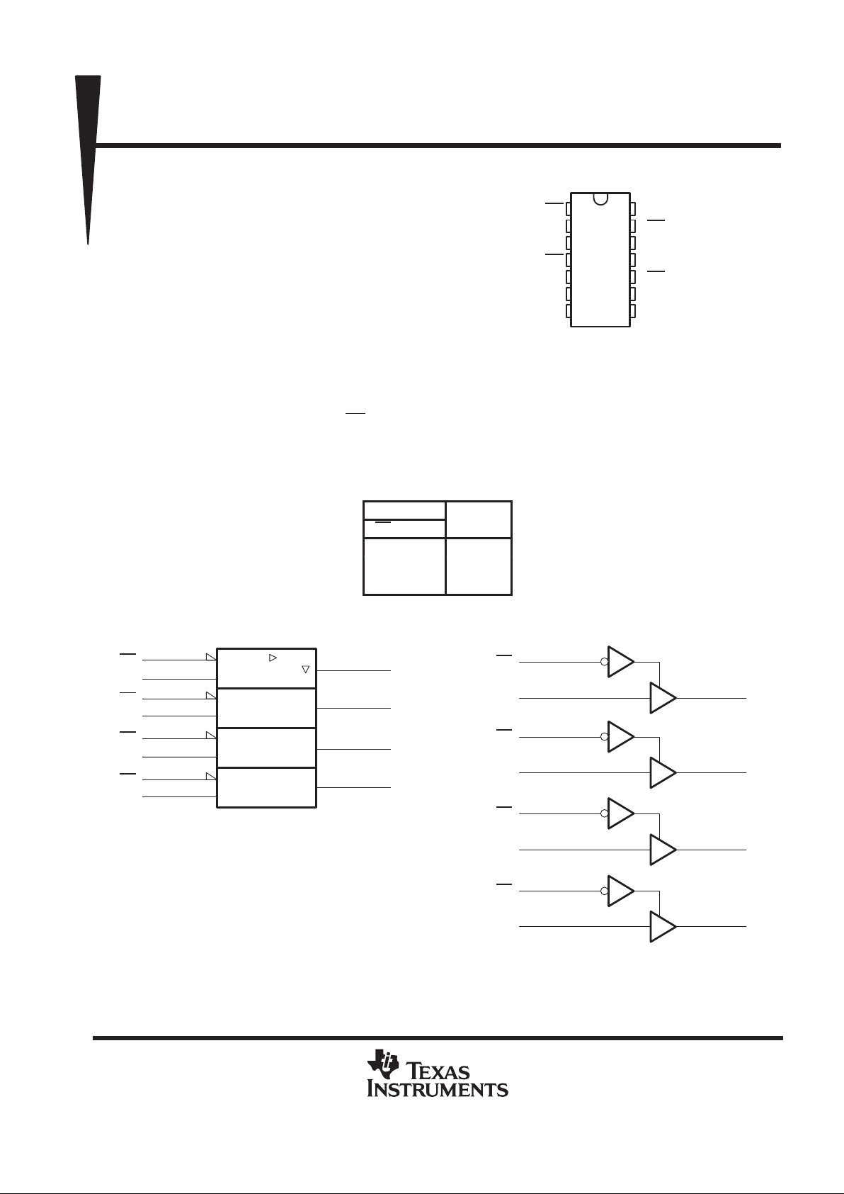
description
The SN64BCT125A bus buffer features independent line drivers with 3-state outputs. Each output is disabled
when the associated output-enable (OE
) input is high.
The SN64BCT125A is characterized for operation from –40°C to 85°C and 0°C to 70°C.
FUNCTION TABLE
(each buffer)
INPUTS
OUTPUT
OE A
Y
L H H
L LL
H X Z
logic symbol
†
logic diagram (positive logic)
1Y
3
EN
1
1OE
2
1A
4
5
2A
10
9
3A
13
12
4A
2Y
6
3Y
8
4Y
11
2OE
3OE
4OE
1
4
56
2A 2Y
2OE
1
23
1A 1Y
1OE
10
98
3A 3Y
3OE
13
12 11
4A 4Y
4OE
†
This symbol is in accordance with ANSI/IEEE Std 91-1984
and IEC Publication 617-12.
D OR N PACKAGE
(TOP VIEW)
1
2
3
4
5
6
7
14
13
12
11
10
9
8
1OE
1A
1Y
2OE
2A
2Y
GND
V
CC
4OE
4A
4Y
3OE
3A
3Y
PRODUCTION DATA information is current as of publication date.
Products conform to specifications per the terms of Texas Instruments
standard warranty. Production processing does not necessarily include
testing of all parameters.
SN64BCT125A
QUADRUPLE BUS BUFFER GATE
WITH 3-STATE OUTPUTS
SCBS052B – JULY 1990 – REVISED MAY 1994
3–4
POST OFFICE BOX 655303 • DALLAS, TEXAS 75265
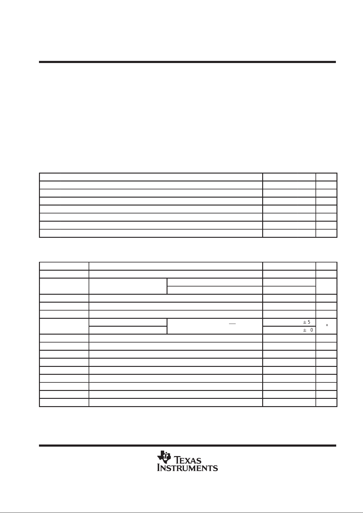
absolute maximum ratings over operating free-air temperature range (unless otherwise noted)
†
Supply voltage range, V
CC
– 0.5 V to 7 V. . . . . . . . . . . . . . . . . . . . . . . . . . . . . . . . . . . . . . . . . . . . . . . . . . . . . . . . . .
Input voltage range, VI (see Note 1) – 0.5 V to 7 V. . . . . . . . . . . . . . . . . . . . . . . . . . . . . . . . . . . . . . . . . . . . . . . . . . .
Voltage range applied to any output in the disabled or power-off state, V
O
– 0.5 V to 5.5 V. . . . . . . . . . . . . . .
Voltage range applied to any output in the high state, V
O
– 0.5 V to V
CC
. . . . . . . . . . . . . . . . . . . . . . . . . . . . . . .
Current into any output in the low state 128 mA. . . . . . . . . . . . . . . . . . . . . . . . . . . . . . . . . . . . . . . . . . . . . . . . . . . . .
Operating free-air temperature range – 40°C to 85°C. . . . . . . . . . . . . . . . . . . . . . . . . . . . . . . . . . . . . . . . . . . . . . . .
Storage temperature range – 65°C to 150°C. . . . . . . . . . . . . . . . . . . . . . . . . . . . . . . . . . . . . . . . . . . . . . . . . . . . . . . .
†
Stresses beyond those listed under “absolute maximum ratings” may cause permanent damage to the device. These are stress ratings only, and
functional operation of the device at these or any other conditions beyond those indicated under “recommended operating conditions” is not
implied. Exposure to absolute-maximum-rated conditions for extended periods may affect device reliability.
NOTE 1: The input and output voltage ratings may be exceeded if the input and output current ratings are observed.
recommended operating conditions
MIN NOM MAX UNIT
V
CC
Supply voltage 4.5 5 5.5 V
V
IH
High-level input voltage 2 V
V
IL
Low-level input voltage 0.8 V
I
IK
Input clamp current –18 mA
I
OH
High-level output current –15 mA
I
OL
Low-level output current 64 mA
T
A
Operating free-air temperature –40 85 °C
electrical characteristics over recommended operating free-air temperature range (unless
otherwise noted)
PARAMETER TEST CONDITIONS MIN TYP‡MAX UNIT
V
IK
VCC = 4.5 V, II = –18 mA –1.2 V
IOH = –3 mA 2.4 3.3
V
OH
V
CC
= 4.5
V
IOH = –15 mA 2 3.1
V
V
OL
VCC = 4.5 V, IOH = 64 mA 0.42 0.55 V
I
OZH
VCC = 5.5 V, VO = 2.7 V 50 µA
I
OZL
VCC = 5.5 V, VO = 0.5 V –50 µA
VCC = 0 to 1.3 V (power up)
"
50
I
OZ
VCC = 1.3 V to 0 (power down)
V
O
= 2.7 V or 0.5 V,
OE at 0.8 V
"
50
µ
A
I
I
VCC = 0, VI = 7 V 0.1 mA
I
IH
VCC = 5.5 V, VI = 2.7 V 25 µA
I
IL
VCC = 5.5 V, VI = 0.5 V –20 µA
I
OS
§
VCC = 5.5 V, VO = 0 –100 –225 mA
I
CCL
VCC = 5.5 V 46 49 mA
I
CCH
VCC = 5.5 V 19 31 mA
I
CCZ
VCC = 5.5 V 6 14 mA
C
i
VCC = 5 V, VI = 2.5 V or 0.5 V 4 pF
C
o
VCC = 5 V, VO = 2.5 V or 0.5 V 9 pF
‡
All typical values are at VCC = 5 V, TA = 25°C.
§
Not more than one output should be tested at a time, and the duration of the test should not exceed one second.
 Loading...