

Texas Instruments SN55976A1WD, SN75976A1DGG, SN75976A1DGGR, SN75976A1DL, SN75976A1DLR Datasheet
...
SN75976A, SN55976A
9-CHANNEL DIFFERENTIAL TRANSCEIVER
SLLS218B – MAY 1995 – REVISED MAY 1997
D
Improved Speed and Package Replacement
for the SN75LBC976
D
Designed to Operate at up to 20 Million
Data Transfers per Second (Fast-20 SCSI)
D
Nine Differential Channels for the Data and
Control Paths of the Small Computer
Systems Interface (SCSI) and Intelligent
Peripheral Interface (IPI)
D
SN75976A Packaged in Shrink
Small-Outline Package with 25-Mil Terminal
Pitch (DL) and Thin Shrink Small-Outline
Package with 20-Mil Terminal Pitch (DGG)
D
SN55976A Packaged in a 56-Pin Ceramic
Flat Pack (WD)
D
Two Skew Limits Available
D
ESD Protection on Bus Terminals
Exceeds 12 kV
D
Low Disabled Supply Current 8 mA Typ
D
Thermal Shutdown Protection
D
Positive- and Negative-Current Limiting
D
Power-Up/Down Glitch Protection
description
The SN75976A is an improved replacement for
the industry’s first 9-channel RS-485
transceiver — the SN75LBC976. The A version
offers improved switching performance, a smaller
package, and higher ESD protection. The
SN75976A is offered in two versions. The ’976A2
skew limits of 4 ns for the differential drivers and
SN75976A DGG or DL
SN55976A WD
(TOP VIEW)
GND
BSR
CRE
1DE/RE
2DE/RE
3DE/RE
4DE/RE
V
GND
GND
GND
GND
GND
V
5DE/RE
6DE/RE
7DE/RE
8DE/RE
9DE/RE
1A
2A
3A
4A
CC
CC
5A
6A
7A
8A
9A
1
2
3
4
5
6
7
8
9
10
11
12
13
14
15
16
17
18
19
20
21
22
23
24
25
26
27
28
56
55
54
53
52
51
50
49
48
47
46
45
44
43
42
41
40
39
38
37
36
35
34
33
32
31
30
29
CDE2
CDE1
CDE0
9B+
–
9B
8B+
–
8B
7B+
7B
–
6B+
6B
–
V
CC
GND
GND
GND
GND
GND
V
CC
5B+
–
5B
4B+
4B
–
3B+
3B
–
2B+
2B
–
1B+
–
1B
5 ns for the differential receivers complies with the
recommended skew budget of the Fast-20 SCSI
standard for data transfer rates up to 20 million
Terminals 13 through 17 and 40 through 44 are
connected together to the package lead frame
and signal ground.
transfers per second. The ’976A1 supports the
Fast SCSI skew budget for 10 million
transfers per second. The skew limit ensures that the propagation delay times, not only from channel-to-channel
but from device-to-device, are closely matched for the tight skew budgets associated with high-speed parallel
data buses.
The patented thermal enhancements made to the 56-pin shrink small-outline package (SSOP) of the SN75976
have been applied to the new, thin shrink, small-outline package (TSSOP). The TSSOP package of fers even
less board area requirements than the SSOP while reducing the package height to 1 mm. This provides more
board area and allows component mounting to both sides of the printed circuit boards for low-profile,
space-restricted applications such as small form-factor hard disk drives.
Please be aware that an important notice concerning availability, standard warranty, and use in critical applications of
Texas Instruments semiconductor products and disclaimers thereto appears at the end of this data sheet.
PRODUCTION DATA information is current as of publication date.
Products conform to specifications per the terms of Texas Instruments
standard warranty. Production processing does not necessarily include
testing of all parameters.
POST OFFICE BOX 655303 • DALLAS, TEXAS 75265
Copyright 1997, Texas Instruments Incorporated
1

SN75976A, SN55976A
T
0°C to 70°C
55°C to 125°C
9-CHANNEL DIFFERENTIAL TRANSCEIVER
SLLS218B – MAY 1995 – REVISED MAY 1997
description (continued)
In addition to speed improvements, the ’976A can withstand electrostatic discharges exceeding 12 kV using
the human-body model, and 600 V using the machine model of MIL-PRF-38535, Method 3015.7 on the RS-485
I/O terminals. This is six times the industry standard and provides protection from the noise that can be coupled
into external cables. The other terminals of the device can withstand discharges exceeding 4 kV and 400 V
respectively.
Each of the nine channels of the ’976A typically meet or exceed the requirements of EIA RS-485 (1983) and
ISO 8482-1987/TIA TR30.2 referenced by American National Standard of Information (ANSI) Systems,
X3.131-1994 (SCSI-2) standard, X2.277-1996 (Fast-20 Parallel Interface), and the Intelligent Peripheral
Interface Physical Layer-ANSI X3.129-1986 standard.
The SN75976A is characterized for operation over an ambient air temperature range of 0°C to 70°C. The
SN55976A is characterized for operation over an ambient air temperature range of –55°C to 125°C.
AVAILABLE OPTIONS
Skew Limit
A
°
°
°
–
†
The R suffix indicates taped and reeled packages.
°
(ns)
Driver Receiver
8 9
4 5
8 9 — — SN55976A1WD
4 5 — — SN55976A2WD
TSSOP
(DGG)
SN75976A1DGG
SN75976A1DGGR
SN75976A2DGG
SN75976A2DGGR
PACKAGE
SN75976A1DL
SN75976A1DLR
SN75976A2DL
SN75976A2DLR
SSOP
(DL)
†
CERAMIC FLAT PACK
(WD)
—
—
2
POST OFFICE BOX 655303 • DALLAS, TEXAS 75265

9-CHANNEL DIFFERENTIAL TRANSCEIVER
g
I/O
Termination
DESCRIPTION
Terminal Functions
SN75976A, SN55976A
SLLS218B – MAY 1995 – REVISED MAY 1997
TERMINAL
NAME NO.
1A to 9A 4,6,8,10,
1B– to 9B– 29,31,33,
1B+ to 9B+ 30,32,34,
BSR 2 TTL Input Pullup BSR is the bit significant response. BSR disables receivers 1 through 8 and
CDE0 54 TTL Input Pulldown CDE0 is the common driver enable 0. Its input signal enables all drivers
CDE1 55 TTL Input Pulldown CDE1 is the common driver enable 1. Its input signal enables drivers
CDE2 56 TTL Input Pulldown CDE2 is the common driver enable 2. When CDE2 is high and BSR is low,
CRE 3 TTL Input Pullup CRE is the common receiver enable. When high, CRE disables receiver
1DE/RE to
9DE/RE
GND 1,13,14,
V
CC
†
Terminal 1 must be connected to signal ground for proper operation.
19,21,23,
25,27
35,37,.46,
48,50,52
36,38,47,
49,51,53
5,7,9,1 1,
20,22,24,
26,28
15,16,17,
40,41,42,
43,44
12,18,39,
45
Logic
Level
TTL I/O Pullup 1A to 9A carry data to and from the communication controller.
RS-485 I/O Pulldown 1B – to 9B – are the inverted data signals of the balanced pair to/from
RS-485 I/O Pullup 1B+ to 9B+ are the noninverted data signals of the balanced pair to/from
TTL Input Pullup 1DE/RE–9DE/RE are direction controls that transmit data to the bus when
NA Power NA GND is the circuit ground. All GND terminals except terminal 1 are
NA Power NA Supply voltage
the bus.
the bus.
enables wired-OR drivers when BSR and DE/RE
high. Channel 9 is placed in a high-impedance state with BSR high.
when CDE0 and 1DE/RE
1 to 4 when CDE1 is high and BSR is low.
drivers 5 to 8 are enabled.
channels 5 to 9.
it and CDE0 are high. Data is received from the bus when
1DE/RE
–9DE/RE and CRE and BSR are low and CDE1 and CDE2 are
low.
physically tied to the die pad for improved thermal conductivity.
– 9DE/RE are high.
and CDE1 or CDE2 are
†
POST OFFICE BOX 655303 • DALLAS, TEXAS 75265
3

SN75976A, SN55976A
9-CHANNEL DIFFERENTIAL TRANSCEIVER
SLLS218B – MAY 1995 – REVISED MAY 1997
logic diagram (positive logic)
54
CDE0
55
CDE1
2
BSR
4
1A
30
29
1B+
1B–
1DE/RE
2A
2DE/RE
3A
3DE/RE
4A
4DE/RE
CDE2
CRE
5A
5DE/RE
6A
6DE/RE
7A
7DE/RE
8A
8DE/RE
9A
9DE/RE
5
6
7
8
9
10
11
56
3
19
20
21
22
23
24
25
26
27
28
Channel 2
Channel 3
Channel 4
Channel 6
Channel 7
Channel 8
2354
BSRBSR
CRE CDE0
32
31
34
33
36
35
38
37
47
46
49
48
51
50
53
52
2B+
2B–
3B+
3B–
4B+
4B–
5B+
5B–
6B+
6B–
7B+
7B–
8B+
8B–
9B+
9B–
4
POST OFFICE BOX 655303 • DALLAS, TEXAS 75265

schematics of inputs and outputs
SN75976A, SN55976A
9-CHANNEL DIFFERENTIAL TRANSCEIVER
SLLS218B – MAY 1995 – REVISED MAY 1997
Input
V
CC
Input
16 V
DE/RE, CRE, BSR, AND
A Inputs
100 kΩ
1 kΩ
8 V
B+ Input B– Input
100 kΩ
18 kΩ
4 kΩ
16 V
B+ AND B– Outputs
2 kΩ
18 kΩ
2 kΩ
V
CC
16 V
V
CC
Output
Input
Input
CDE0, CDE1, AND CDE2 Inputs
1 kΩ
100 kΩ
18 kΩ
100 kΩ
4 kΩ
A Output
V
8 V
16 V
16 V
CC
40 Ω
2 kΩ
V
CC
Output
V
CC
4 kΩ
16 V
POST OFFICE BOX 655303 • DALLAS, TEXAS 75265
8 V
5

SN75976A, SN55976A
Junction-to-ambient thermal resistance, R
Junction-to-case thermal resistance, R
9-CHANNEL DIFFERENTIAL TRANSCEIVER
SLLS218B – MAY 1995 – REVISED MAY 1997
absolute maximum ratings over operating free-air temperature range (unless otherwise noted)
Supply voltage range, V
Bus voltage range –10 V to 15 V. . . . . . . . . . . . . . . . . . . . . . . . . . . . . . . . . . . . . . . . . . . . . . . . . . . . . . . . . . . . . . . . . .
Data I/O and control (A side) voltage range –0.3 V to V
Electrostatic discharge:B side and GND, Class 3, A: (see Note 2) 12 kV. . . . . . . . . . . . . . . . . . . . . . . . . . . . . . .
Continuous total power dissipation (see Note 3) internally limited. . . . . . . . . . . . . . . . . . . . . . . . . . . . . . . . . . . . . .
Storage temperature range, T
Lead temperature 1,6 mm (1/16 inch) from case for 10 seconds 260°C. . . . . . . . . . . . . . . . . . . . . . . . . . . . . . .
†
Stresses beyond those listed under “absolute maximum ratings” may cause permanent damage to the device. These are stress ratings only, and
functional operation of the device at these or any other conditions beyond those indicated under “recommended operating conditions” is not
implied. Exposure to absolute-maximum-rated conditions for extended periods may affect device reliability.
NOTES: 1. All voltage values are with respect to the GND terminals.
2. This absolute maximum rating is tested in accordance with MIL-PRF-38535, Method 3015.7.
3. The maximum operating junction temperature is internally limited. Use the Dissipation Rating Table to operate below this
temperature.
PACKAGE
DGG 2500 mW 20 mW/°C 1600 mW —
DL 2500 mW 20 mW/°C 1600 mW —
WD 1300 mW 10.5 mW/°C 827 mW 250 mW
‡
This is the inverse of the junction-to-ambient thermal resistance when board-mounted and with no air flow.
(see Note 1) –0.3 V to 6 V. . . . . . . . . . . . . . . . . . . . . . . . . . . . . . . . . . . . . . . . . . . . . .
CC
CC
B side and GND, Class 3, B: (see Note 2) 400 V. . . . . . . . . . . . . . . . . . . . . . . . . . . . . . .
All terminals, Class 3, A: 4 kV. . . . . . . . . . . . . . . . . . . . . . . . . . . . . . . . . . . . . . . . . . . . . . .
All terminals, Class 3, B: 400 V. . . . . . . . . . . . . . . . . . . . . . . . . . . . . . . . . . . . . . . . . . . . .
–65°C to 150°C. . . . . . . . . . . . . . . . . . . . . . . . . . . . . . . . . . . . . . . . . . . . . . . . . . .
stg
DISSIPATION RATING TABLE
TA ≤ 25°C
OPERATING FACTOR
ABOVE TA = 25°C
‡
TA = 70°C
POWER RATING
TA = 125°C
POWER RATING
+0.5 V. . . . . . . . . . . . . . . . . . . . . . . . . . . . . . . . . . . . .
†
package thermal characteristics
θJA
Junction-to-ambient thermal resistance, R
Junction-to-case thermal resistance, R
Thermal-shutdown junction temperature, T
θJA
θJC
θJC
JS
MIN NOM MAX UNIT
DGG, board-mounted, no air flow 50 °C/W
DL, board-mounted, no air flow 50 °C/W
WD 95.4 °C/W
DGG 27 °C/W
DL 12 °C/W
WD 5.67 °C/W
165 °C
6
POST OFFICE BOX 655303 • DALLAS, TEXAS 75265

recommended operating conditions
Voltage at any bus terminal (separately or common-mode), V
V
V
nB+ or nB
High-level output current, I
Low-level output current, I
Operating free-air temperature, T
Supply voltage, V
High-level input voltage, V
Low-level input voltage, V
Operating case temperature, T
p
†
n = 1 – 9
CC
IH
IL
p
p
p
OH
OL
C
p
A
SN75976A, SN55976A
9-CHANNEL DIFFERENTIAL TRANSCEIVER
SLLS218B – MAY 1995 – REVISED MAY 1997
MIN NOM MAX UNIT
4.75 5 5.25 V
Except nB+, nB–
Except nB+, nB–
,
, or
O
I
IC
Driver –60 mA
Receiver –8 mA
Driver 60 mA
Receiver 8 mA
SN75976A 0 125 °C
SN75976A 0 70 °C
SN55976A –55 125 °C
†
†
–
2 V
0.8 V
12 V
–7 V
POST OFFICE BOX 655303 • DALLAS, TEXAS 75265
7

SN75976A, SN55976A
PARAMETER
TEST CONDITIONS
UNIT
level out ut voltage
level out ut voltage
OH
age
OL
age
IIBus input current
I
g
IILLow-level input current
I
g
C
capacitance
9-CHANNEL DIFFERENTIAL TRANSCEIVER
SLLS218B – MAY 1995 – REVISED MAY 1997
electrical characteristics over recommended operating free-air temperature range (unless
otherwise noted)
SN55976A SN75976A
MIN TYP†MAX MIN TYP†MAX
S1 to A, VT = 5 V, See Figure 1 0.7 1 1.8 V
V
V
V
V
V
V
V
I
I
C
†
NOTE 4: Cpd determines the no-load dynamic supply current consumption, IS = CPD × VCC × f + I
Driver differential high-
ODH
ODL
IT+
IT–
hys
IH
OS
OZ
CC
O
pd
All typical values are at VCC = 5 V, TA = 25°C.
p
Driver differential low-
p
High-level output volt-
Low-level output volt-
Receiver positive-going differential input
threshold voltage
Receiver negativegoing differential input
threshold voltage
Receiver input
hysteresis
(V
– V
IT+
High-level input current
Short circuit output
current
High-impedance-state
output current
Supply current
Output capacitance nB+ or nB– to GND 18 18 25 pF
Power dissipation
p
(see Note 4)
)
IT–
p
p
S1 to B,
TC ≥ 25°C
S1 to B,
See Figure 1
S1 to A,
TC ≥ 25°C
S1 to B, VT = 5 V, See Figure 1 0.7 –1.8 –1 –1.8 V
S1 to A,
See Figure 1
A side,
IOH = –8 mA
B side, VT = 5 V, See Figure 1 3 3 V
A side,
IOH = 8 mA
A side, VT = 5 V, See Figure 1 1 1 V
IOH = –8 mA, See Figure 3 0.2 0.2 V
IOL = 8 mA, See Figure 3 –0.2 –0.2 V
VCC = 5 V, TA = 25°C 24 45 24 45 mV
VIH = 12 V, VCC = 5 V, Other input at 0 V 0.4 1 0.4 1 mA
VIH = 12 V, VCC = 0, Other input at 0 V 0.5 1 0.5 1 mA
VIH = –7 V, VCC = 5 V, Other input at 0 V –0.4 –0.8 –0.4 –0.8 mA
VIH = –7 V, VCC = 0, Other input at 0 V –0.3 –0.8 –0.3 –0.8 mA
A, BSR, DE/RE, and CRE, VIH = 2 V –100 –100 µA
CDE0, CDE1, and CDE2,
A, BSR, DE/RE, and CRE, VIL = 0.8 V –100 –100 µA
CDE1, CDE1, and CDE2, VIL = 0.8 V 100 100 µA
nB+ or nB– ±260 ±260 mA
A See IIH and I
nB+ or nB–
Disabled 10 10 mA
All drivers enabled, no load
All receivers enabled, no load 45 45 mA
Receiver 40 40 pF
Driver 100 100 pF
VT = 5 V,
See Figure 1
VT = 5 V,
VT = 5 V,
See Figure 1
VT = 5 V,
VID = 200 mV,
See Figure 3
VID = –200 mV,
See Figure 3
VIH = 2V 100 100 µA
0.7 0.8 V
0.7 –1.4 –1 –1.4 V
–0.8 –1.4 –0.8 –1.4 V
4 4.5 4 4.5 V
0.6 0.8 0.6 0.8 V
IL
See I
I
60 60 mA
CC
1 1.4 V
See IIH and I
See I
IL
I
8
POST OFFICE BOX 655303 • DALLAS, TEXAS 75265

SN75976A, SN55976A
PARAMETER
TEST CONDITIONS
UNIT
t
gy,
PHL PLH
t
,
dd
See Figures 5 and 6
PARAMETER
TEST CONDITIONS
UNIT
t
gy,
PHL PLH
t
,
dd
See Figures 5 and 6
9-CHANNEL DIFFERENTIAL TRANSCEIVER
SLLS218B – MAY 1995 – REVISED MAY 1997
driver switching characteristics over recommended operating conditions (unless otherwise
noted)
SN75976A
MIN TYP†MAX
2.5 13.5 ns
’976A1
pd
sk(lim)
t
sk(p)
t
f
t
r
t
en
t
dis
t
PHZ
t
PLZ
t
PZH
t
PZL
†
All typical values are at VCC = 5 V, TA = 25°C.
NOTE 5: This parameter is applicable at one VCC and operating temperature within the recommended operating conditions and to any two
Propagation delay time, t
(see Figures 1 and 2)
Skew limit, maximum tp – minimum tp
(see Note 5)
Pulse skew, |t
Fall time S1 to B, See Figure 2 4 ns
Rise time See Figure 2 8 ns
Enable time, control inputs to active output 50 ns
Disable time, control inputs to high-impedance output 100 ns
Propagation delay time, high-level to high-impedance output 17 100 ns
Propagation delay time, low-level to high-impedance output
Propagation delay time, high-impedance to high-level output
Propagation delay time, high-impedance to low-level output 17 50 ns
devices.
PHL
– t
or t
’976A2
’976A1 8 ns
’976A2
| 4 ns
PLH
VCC = 5 V, TC = 25°C 3 11 ns
VCC = 5 V, TC = 100°C 5 13 ns
4.5 11.5 ns
VCC = 5 V, TC = 25°C 5 9 ns
VCC = 5 V, TC = 100°C 7 11 ns
4 ns
25 100 ns
17 50 ns
driver switching characteristics over recommended operating conditions (unless otherwise
noted)
SN55976A
MIN TYP†MAX
pd
sk(lim)
t
sk(p)
t
f
t
r
t
en
t
dis
t
PHZ
t
PLZ
t
PZH
t
PZL
†
All typical values are at VCC = 5 V, TA = 25°C.
NOTE 5. This parameter is applicable at one VCC and operating temperature within the recommended operating conditions and to any two
Propagation delay time, t
(see Figures 1 and 2)
Skew limit, maximum tp – minimum tp
(see Note 5)
Pulse skew, |t
Fall time S1 to B, See Figure 2 4 ns
Rise time See Figure 2 8 ns
Enable time, control inputs to active output 60 ns
Disable time, control inputs to high-impedance output 140 ns
Propagation delay time, high-level to high-impedance output 120 ns
Propagation delay time, low-level to high-impedance output
Propagation delay time, high-impedance to high-level output
Propagation delay time, high-impedance to low-level output 60 ns
devices.
PHL
– t
or t
| 4 ns
PLH
’976A1 VCC = 5 V, TA = 25°C 15 ns
’976A2
’976A1 8 ns
’976A2
VCC = 5 V, TA = 25°C 13.5 ns
4 ns
120 ns
60 ns
POST OFFICE BOX 655303 • DALLAS, TEXAS 75265
9

SN75976A, SN55976A
PARAMETER
TEST CONDITIONS
UNIT
t
gy,
PHL PLH
t
,
dd
See Figures 7 and 8
PARAMETER
TEST CONDITIONS
UNIT
t
gy,
PHL PLH
t
,
dd
See Figures 7 and 8
9-CHANNEL DIFFERENTIAL TRANSCEIVER
SLLS218B – MAY 1995 – REVISED MAY 1997
receiver switching characteristics over recommended operating conditions (unless otherwise
noted)
SN75976A
MIN TYP†MAX
’976A1 7.5 16.5 ns
pd
sk(lim)
t
sk(p)
t
t
t
en
t
dis
t
PHZ
t
PLZ
t
PZH
t
PZL
†
All typical values are at VCC = 5 V, TA = 25°C.
NOTE 5. This parameter is applicable at one VCC and operating temperature within the recommended operating conditions and to any two
Propagation delay time, t
(see Figures 3 and 4)
Skew limit, maximum tp – minimum tp
(see Note 5)
Pulse skew, |t
Transition time (tr or tf) See Figure 4 2 ns
Enable time, control inputs to active output 50 ns
Disable time, control inputs to high-impedance output 60 ns
Propagation delay time, high-level to high-impedance output 60 ns
Propagation delay time, low-level to high-impedance output
Propagation delay time, high-impedance to high-level output
Propagation delay time, high-impedance to low-level output 50 ns
devices.
PHL
– t
or t
’976A2
’976A1 9 ns
’976A2
| 0.6 4 ns
PLH
VCC = 5 V, TC = 25°C 8.6 13.6 ns
VCC = 5 V, TC = 100°C 9 14 ns
8.5 14.5 ns
5 ns
50 ns
50 ns
receiver switching characteristics over recommended operating conditions (unless otherwise
noted)
SN55976A
MIN TYP†MAX
pd
sk(lim)
t
sk(p)
t
t
t
en
t
dis
t
PHZ
t
PLZ
t
PZH
t
PZL
†
All typical values are at VCC = 5 V, TA = 25°C.
NOTE 5. This parameter is applicable at one VCC and operating temperature within the recommended operating conditions and to any two
Propagation delay time, t
(see Figures 3 and 4)
Skew limit, maximum tp – minimum tp
(see Note 5)
Pulse skew, |t
Transition time (tr or tf) See Figure 4 2 ns
Enable time, control inputs to active output 70 ns
Disable time, control inputs to high-impedance output 80 ns
Propagation delay time, high-level to high-impedance output 80 ns
Propagation delay time, low-level to high-impedance output
Propagation delay time, high-impedance to high-level output
Propagation delay time, high-impedance to low-level output 70 ns
devices.
PHL
– t
or t
| 0.6 4 ns
PLH
’976A1 VCC = 5 V, TA = 25°C 19 ns
’976A2
’976A1 9 ns
’976A2
VCC = 5 V, TA = 25°C 16 ns
5 ns
70 ns
70 ns
10
POST OFFICE BOX 655303 • DALLAS, TEXAS 75265

9-CHANNEL DIFFERENTIAL TRANSCEIVER
SLLS218B – MAY 1995 – REVISED MAY 1997
PARAMETER MEASUREMENT INFORMATION
SN75976A = 5 V
SN55976A = 4.5 V
SN75976A, SN55976A
AB
B+
I
I
I
Input
(see Note A)
†
CDE0 and DE/RE
‡
For the SN75976A only, all nine drivers are enabled, similarly loaded, and switching.
A
V
I
are at 2 V, BSR is at 0.8 V and, for the SN75976A only , all others are open.
O
V
OD
V
I
O
B–
V
†
O
15 pF
75 Ω
O
15 pF
S1
165 Ω
375 Ω
S2
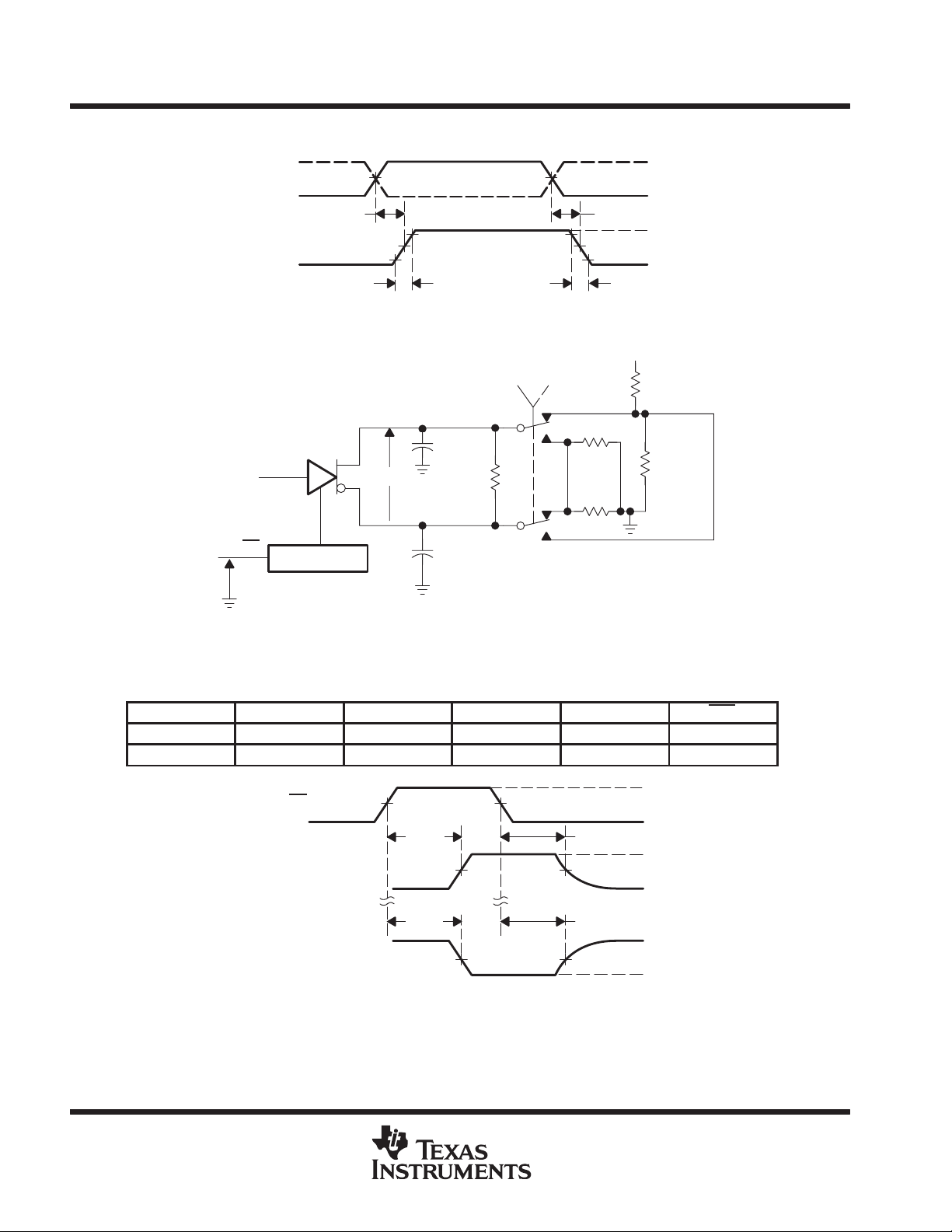
Figure 1. Driver Test Circuit, Currents, and Voltages
Output, V
Input
OD
t
PLH
1.5 V 1.5 V
90% 90%
0V
10%
t
r
t
PHL
0V
10%
t
f
‡
3 V
0 V
V
OD(H)
V
OD(L)
165 Ω
375 Ω
S1 to A or B
Figure 2. Driver Delay and Transition Time Test Waveforms
V
ID
Input B+
†
I
O
Output
V
O
CL = 15 pF
‡
Generator
(see Note A)
Generator
(see Note A)
†
CDE0, CDE1, CDE2, BSR, CRE, and DE/RE at 0.8 V
‡
For the SN75976A only, all nine receivers are enabled and switching.
50 Ω
Input B–
50 Ω
Figure 3. Receiver Propagation Delay and Transition Time Test Circuit
NOTES: A. All input pulses are supplied by a generator having the following characteristics: tr ≤ 6 ns, tf ≤ 6 ns, PRR ≤ 1 MHz, duty cycle = 50%,
ZO = 50 Ω.
B. All resistances are in Ω and ± 5%, unless otherwise indicated.
C. All capacitances are in pF and ± 10%, unless otherwise indicated.
D. All indicated voltages are ± 10 mV.
POST OFFICE BOX 655303 • DALLAS, TEXAS 75265
11
SN75976A, SN55976A
9-CHANNEL DIFFERENTIAL TRANSCEIVER
SLLS218B – MAY 1995 – REVISED MAY 1997
PARAMETER MEASUREMENT INFORMATION
0 V or 3 V
DE/RE
Input
Input B–
Input B+
Output
t
PLH
1.5 V 1.5 V
1.4 V
10%
t
r
90% 90%
t
PHL
1.4 V
10%
t
f
Figure 4. Receiver Delay and Transition Time Waveforms
4.5 V
AB
S1
165 Ω
375 Ω
S2
†
A
See Table 1
B+
B–
50 pF
V
OD
75 Ω
50 pF
3 V
0 V
V
OH
V
OL
165 Ω
375 Ω
†
Includes probe and jig capacitance in two places.
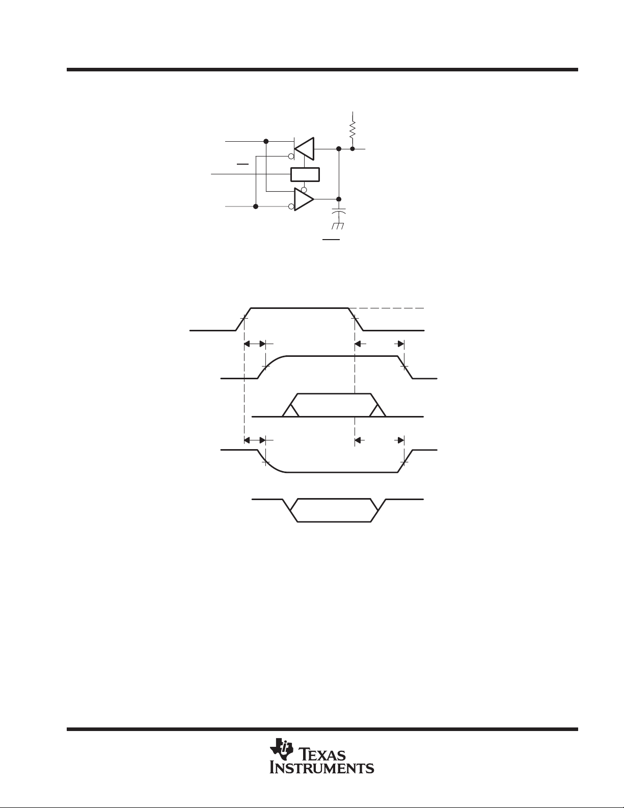
Figure 5. Driver Enable and Disable Time Test Circuit
Table 1. Enabling For Driver Enable And Disable Time
DRIVER BSR CDE0 CDE1 CDE2 CRE
1 – 8 H H L L X
9 L H H H H
Input, DE/RE
Output, V
Output, V
OD
OD
1.5 V 1.5 V
t
PZH
0 V
t
PZL
0 V
0 V
t
0 V
t
PHZ
PLZ
3 V
0 V
V
OD(H)
∼ –1 V
∼ 1 V
V
OD(L)
A at 3V
S1 to B
A at 0V
S1 to A
Figure 6. Driver Enable Time Waveforms
NOTES: A. All input pulses are supplied by a generator having the following characteristics: tr ≤ 6 ns, tf ≤ 6 ns, PRR ≤ 1 MHz, duty cycle = 50%,
ZO = 50 Ω.
B. All resistances are in Ω and ± 5%, unless otherwise indicated.
C. All capacitances are in pF and ± 10%, unless otherwise indicated.
D. All indicated voltages are ± 10 mV.
12
POST OFFICE BOX 655303 • DALLAS, TEXAS 75265
9-CHANNEL DIFFERENTIAL TRANSCEIVER
SLLS218B – MAY 1995 – REVISED MAY 1997
PARAMETER MEASUREMENT INFORMATION
V
T
SN75976A, SN55976A
0 V or 3 V
Input
3 V or 0 V
†
CDE0 is high, CDE1, CDE2, BSR, and CRE
the SN75976A only, all others are open.
‡
Includes probe and jig capacitance.
B+
DE/RE
B–
†
620 Ω
A
Output
‡
40 pF
are low and, for
Figure 7. Receiver Enable and Disable Time Test Circuit
Input
Output
V
OD
1.4 V 1.4 V
t
PLZ
1.4 V 1.4 V
Indeterminate
t
PZL
3 V
0 V
B+ at 0 V
B– at 3 V
VT = V
CC
Output
V
OD
t
PHZ
1.4 V 1.4 V
Indeterminate
t
PZH
B+ at 3 V
B– at 0 V
VT = 0
Figure 8. Receiver Enable and Disable Time Waveforms
NOTES: A. All input pulses are supplied by a generator having the following characteristics: tr ≤ 6 ns, tf ≤ 6 ns, PRR ≤ 1 MHz, duty cycle = 50%,
ZO = 50 Ω.
B. All resistances are in Ω and ± 5%, unless otherwise indicated.
C. All capacitances are in pF and ± 10%, unless otherwise indicated.
D. All indicated voltages are ± 10 mV.
POST OFFICE BOX 655303 • DALLAS, TEXAS 75265
13

SN75976A, SN55976A
9-CHANNEL DIFFERENTIAL TRANSCEIVER
SLLS218B – MAY 1995 – REVISED MAY 1997
TYPICAL CHARACTERISTICS
AVERAGE SUPPLY CURRENT
vs
FREQUENCY
250
200
150
100
– Average Supply Current – mA
50
CC
I
0
0.001 0.01 0.1 1 10 100
9 Drivers
9 Receivers
f – Frequency – MHz
Figure 9
BUS
INPUT CURRENT
vs
INPUT VOLTAGE
15
LOGIC INPUT CURRENT
INPUT VOLTAGE
–30
A, DE/RE,CRE,BSR
–25
AµI
–20
–15
–10
– Logic Input Current –
I
–5
0
0123
VI – Input Voltage – V
Figure 10
LOW-LEVEL OUTPUT VOLTAGE
LOW-LEVEL OUTPUT CURRENT
2.5
vs
45
DRIVER
vs
10
5
0
– Input Current – mA
I
I
–5
–10
–20 –15 –10 –5 0 5 10 15 20
14
VI – Input Voltage – V
Figure 11
POST OFFICE BOX 655303 • DALLAS, TEXAS 75265
2
1.5
1
– Low-Level Output Voltage – V
0.5
OL
V
0
0 102030405060
IOL – Low-Level Output Current – mA
Figure 12
70 80 90 100

9-CHANNEL DIFFERENTIAL TRANSCEIVER
TYPICAL CHARACTERISTICS
SN75976A, SN55976A
SLLS218B – MAY 1995 – REVISED MAY 1997
DRIVER
HIGH-LEVEL OUTPUT VOLTAGE
vs
HIGH-LEVEL OUTPUT CURRENT
4
3.5
3
2.5
2
1.5
1
– High-Level Output Voltage – V
OH
V
0.5
0
0 –20 – 40 –60 –80 –100
IOH – High-Level Output Current – mA
Figure 13
DRIVER
AVERAGE DIFFERENTIAL OUTPUT VOLTAGE
vs
AVERAGE CASE TEMPERATURE
2.5
2
1.5
1
0.5
– Average Differential Output Voltage – V
OD
V
||
S1 to Position B (see Figure 1)
0
0 40 60 100
V
, VCC = 5.25 V
OD(L)
V
, VCC = 4.75 V
OD(L)
V
, VCC = 5.25 V
OD(H)
V
, VCC = 4.75 V
OD(H)
20 80 120
TC – Average Case Temperature – °C
Figure 14
140
PROPAGATION DELAY TIME
CASE TEMPERATURE
16
14
12
10
8
6
– Propagation Delay Time – ns
pd
t
(Data Extracted From 7 Wafer Lots)
4
VCC = 5 V
2
0 20406080
t
PHL(max)
t
PHL(min)
TC – Case Temperature – °C
Figure 15
RECEIVER
vs
t
PLH(max)
t
PLH(min)
100 120 140
PROPAGATION DELAY TIME
CASE TEMPERATURE
14
VCC = 5 V,
S1 to Position B (see Figure 1)
12
t
10
8
6
t
PLH(min)
4
– Propagation Delay Time – ns
pd
t
2
Data Extracted From 7 Wafer Lots
0
0 20406080
PHL(max)
TC – Case Temperature – °C
Figure 16
DRIVER
vs
t
PHL(min)
t
PLH(max)
100 120 140
POST OFFICE BOX 655303 • DALLAS, TEXAS 75265
15

SN75976A, SN55976A
9-CHANNEL DIFFERENTIAL TRANSCEIVER
SLLS218B – MAY 1995 – REVISED MAY 1997
TYPICAL CHARACTERISTICS
OUTPUT CURRENT
SUPPLY VOLTAGE
100
–20
– Output Current – mA
O
I
–40
TA = 25°C
80
60
40
20
0
DRIVER
vs
I
OH
–60
–80
01 23
VCC – Supply Voltage – V
Figure 17
I
OL
456
16
POST OFFICE BOX 655303 • DALLAS, TEXAS 75265

SN75976A, SN55976A
9-CHANNEL DIFFERENTIAL TRANSCEIVER
SLLS218B – MAY 1995 – REVISED MAY 1997
APPLICATION INFORMATION
Table 2. Typical Signal and Terminal Assignments
SIGNAL TERMINAL SCSI DATA SCSI CONTROL IPI DATA IPI CONTROL
CDE0 54 DIFFSENSE DIFFSENSE V
CDE1 55 GND GND XMTA, XMTB GND
CDE2 56 GND GND XMTA, XMTB SLAVE/MASTER
BSR 2 GND GND GND, BSR GND
CRE 3 GND GND GND V
1A 4 DB0, DB8 ATN AD7, BD7 NOT USED
1DE/RE 5 DBE0, DBE8 INIT EN GND GND
2A 6 DB1, DB9 BSY AD6, BD6 NOT USED
2DE/RE 7 DBE1, DBE9 BSY EN GND GND
3A 8 DB2, DB10 ACK AD5, BD5 SYNC IN
3DE/RE 9 DBE2, DBE10 INIT EN GND GND
4A 10 DB3, DB11 RST AD4, BD4 SLAVE IN
4DE/RE 11 DBE3, DBE11 GND GND GND
5A 19 DB4, DB12 MSG AD3, BD3 NOT USED
5DE/RE 20 DBE4, DBE12 TARG EN GND GND
6A 21 DB5, DB13 SEL AD2, BD2 SYNC OUT
6DE/RE 22 DBE5, DBE13 SEL EN GND GND
7A 23 DB6, DB14 C/D AD1, BD1 MASTER OUT
7DE/RE 24 DBE6, DBE14 TARG EN GND GND
8A 25 DB7, DB15 REQ AD0, BD0 SELECT OUT
8DE/RE 26 DBE7, DBE15 TARG EN GND GND
9A 27 DBP0, DBP1 I/O AP, BP ATTENTION IN
9DE/RE 28 DBPE0, DBPE1 TARG EN XMT A, XMTB V
ABBREVIATIONS:
DBn = data bit n, where n = (0,1, . . . ,15)
DBEn = data bit n enable, where n = (0,1, . . . ,15)
DBP0 = parity bit for data bits 0 through 7 or IPI bus A
DBPE0 = parity bit enable for P0
DBP1 = parity bit for data bits 8 through 15 or IPI bus B
DBPE1 = parity bit enable for P1
ADn or BDn = IPI Bus A – Bit n (ADn) or Bus B – Bit n (BDn), where n = (0,1, ...,7)
AP or BP = IPI parity bit for bus A or bus B
XMTA or XMTB = transmit enable for IPI bus A or B
BSR = bit significant response
INIT EN = common enable for SCSI initiator mode
TARG EN = common enable for SCSI target mode
NOTE A: Signal inputs are shown as active high. When only active-low inputs are available, logic inversion
is accomplished by reversing the B+ and B– connector terminal assignments.
CC
V
CC
CC
CC
POST OFFICE BOX 655303 • DALLAS, TEXAS 75265
17
SN75976A, SN55976A
9-CHANNEL DIFFERENTIAL TRANSCEIVER
SLLS218B – MAY 1995 – REVISED MAY 1997
APPLICATION INFORMATION
Function Tables
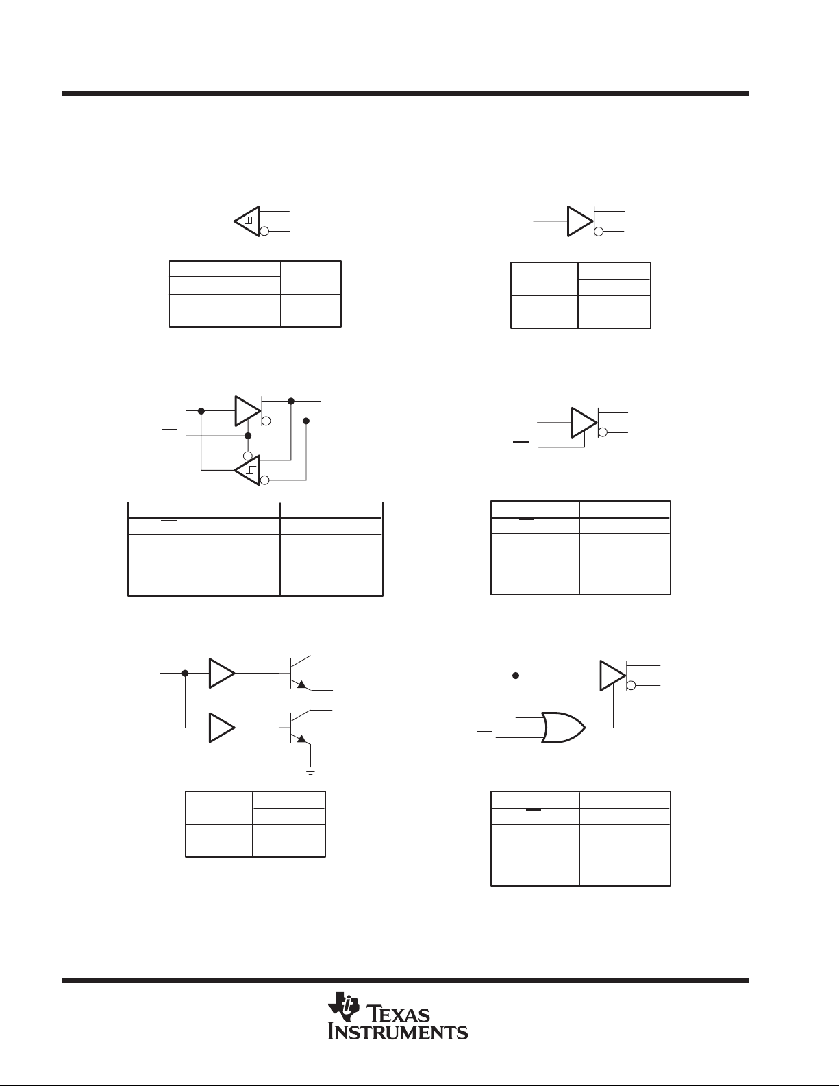
RECEIVER DRIVER
A
INPUTS
†
B+
L
H
A
DE/RE
INPUTS OUTPUTS
L
L
H
H
AB+
–
–
L
H
DE/RE
†
B–
H
L
TRANSCEIVER DRIVER WITH ENABLE
†
†
B–
L
H
H
L
–
–
–
–
B+
B–
OUTPUT
A
L
H
B+
B–
AB+
L
–
H
–
–
L
–
H
B–
–
–
H
L
A
L
H
L
H
OUTPUTS
B+ B–
LHH
Z
Z
L
H
INPUT
A
L
H
A
DE/RE
INPUTS OUTPUTS
DE/RE AB+
L
L
H
H
B+
B–
L
B+
B–
B–
Z
Z
H
L
WIRED-OR DRIVER TWO-ENABLE INPUT DRIVER
A
B+
B–
INPUT
A
L
H
H = high level, L = low level, X = irrelevant, Z = high impedance (off)
†
An H in this column represents a voltage of 200 mV or higher than the other bus input. An L represents a voltage of 200 mV or lower than the
other bus input. Any voltage less than 200 mV results in an indeterminate receiver output.
OUTPUTS
B+ B–
Z
H
Z
L
DE/RE
A
INPUTS OUTPUTS
DE/RE AB+
L
L
H
L
L
H
H
H
Z
H
L
H
B+
B–
B–
Z
L
H
L
18
POST OFFICE BOX 655303 • DALLAS, TEXAS 75265
9-CHANNEL DIFFERENTIAL TRANSCEIVER
APPLICATION INFORMATION
SN75976A, SN55976A
SLLS218B – MAY 1995 – REVISED MAY 1997
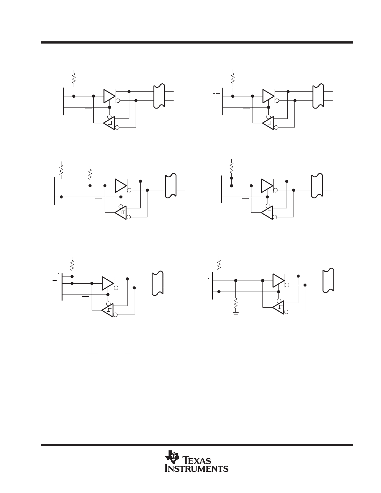
V
CC
†
620 Ω
I/O
EN
V
CC
620 Ω
I
O
(c) WIRED-OR DRIVER AND ACTIVE-HIGH INPUT
nA
nDE/RE
(a) ACTIVE-HIGH BIDIRECTIONAL I/O
WITH SEPARATE ENABLE
V
CC
†
nDE/RE
620 Ω
nA
†
SCSI
Connector
nB+
nB–
nB+
nB–
+
–
SCSI
Connector
V
CC
†
620 Ω
I
/O
EN
+
–
I
‡
O
EN
(d) SEPARATE ACTIVE-HIGH INPUT, OUTPUT,
nA
nDE/RE
(b) ACTIVE-LOW BIDIRECTIONAL I/O
WITH SEPARATE ENABLE
V
CC
†
620 Ω
nA
nDE/RE
AND ENABLE
SCSI
Connector
nB+
nB–
SCSI
Connector
nB+
nB–
–
+
+
–
V
CC
†
620 Ω
I
‡
O
EN
†
When 0 is open drain
‡
Must be open-drain or 3-state output
NOTE A: The BSR, CRE
nA
nDE/RE
(e) SEPARATE ACTIVE-LOW INPUT AND
OUTPUT AND ACTIVE-HIGH ENABLE
, A, and DE/RE inputs have internal pullup resistors. CDE0, CDE1, and CDE2 have internal pulldown resistors.
V
CC
SCSI
Connector
nB+
nB–
–
+
I
O
620 Ω
(f) WIRED-OR DRIVER AND ACTIVE-LOW INPUT
620 Ω
†
nA
nDE/RE
Figure 18. Typical SCSI Transceiver Connections
Connector
nB+
nB–
SCSI
–
+
POST OFFICE BOX 655303 • DALLAS, TEXAS 75265
19

SN75976A, SN55976A
9-CHANNEL DIFFERENTIAL TRANSCEIVER
SLLS218B – MAY 1995 – REVISED MAY 1997
APPLICATION INFORMATION
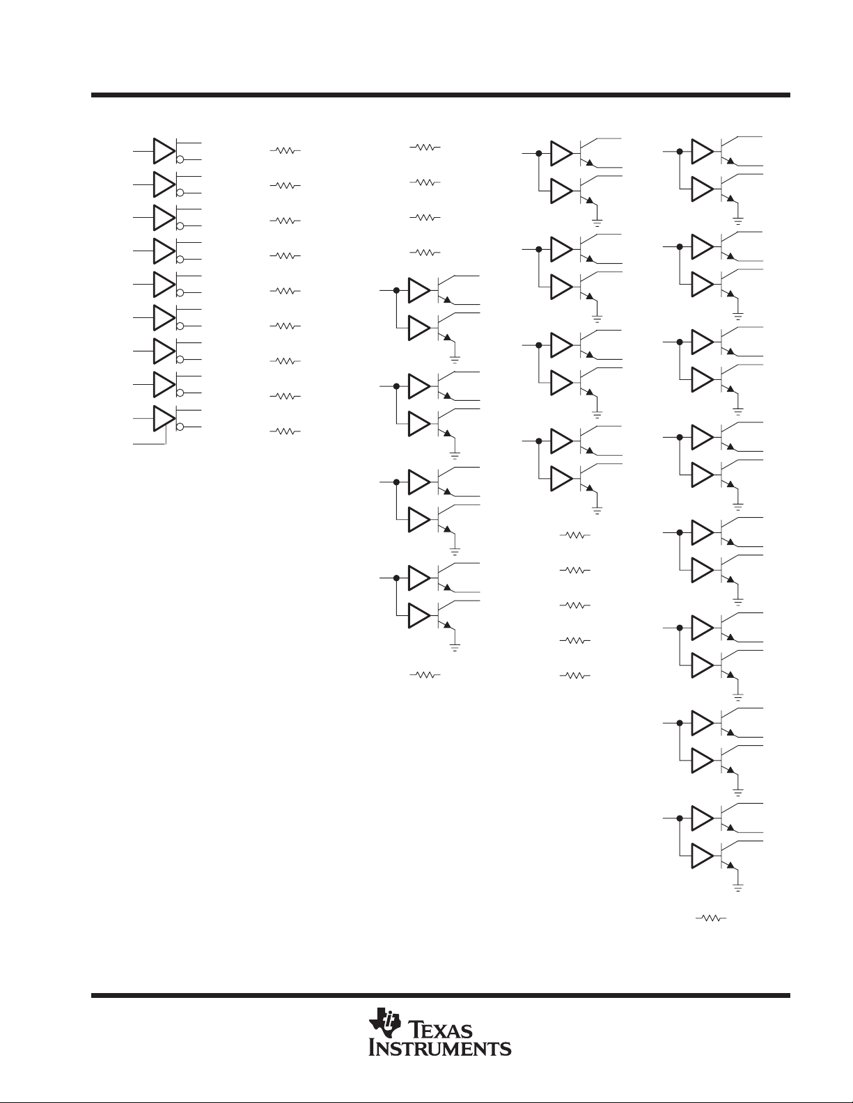
channel logic configurations with control input logic
The following logic diagrams show the positive-logic representation for all combinations of control inputs. The
control inputs are from MSB to LSB; the BSR, CDE0, CDE1, CDE2, and CRE
diagrams. Channel 1 is at the top of the logic diagrams; channel 9 is at the bottom of the logic diagrams.
Hi-Z
bit values are shown below the
Hi-Z
Hi-Z
Hi-Z
Hi-ZHi-Z
Figure 19. 00000 Figure 20. 00001 Figure 21. 00010 Figure 22. 00011 Figure 23. 00100
20
POST OFFICE BOX 655303 • DALLAS, TEXAS 75265

Hi-Z
Hi-Z
Hi-Z
Hi-Z
SN75976A, SN55976A
9-CHANNEL DIFFERENTIAL TRANSCEIVER
SLLS218B – MAY 1995 – REVISED MAY 1997
APPLICATION INFORMATION
Hi-Z Hi-Z
Figure 24. 00101 Figure 25. 00110 Figure 26. 00111
Figure 28. 01001
Figure 27. 01000
POST OFFICE BOX 655303 • DALLAS, TEXAS 75265
21

SN75976A, SN55976A
9-CHANNEL DIFFERENTIAL TRANSCEIVER
SLLS218B – MAY 1995 – REVISED MAY 1997
APPLICATION INFORMATION
Figure 29. 01010 Figure 30. 01011 Figure 31. 01100
Figure 32. 01101 Figure 33. 01110
22
POST OFFICE BOX 655303 • DALLAS, TEXAS 75265
Hi-Z
SN75976A, SN55976A
9-CHANNEL DIFFERENTIAL TRANSCEIVER
SLLS218B – MAY 1995 – REVISED MAY 1997
APPLICATION INFORMATION
Hi-Z
Figure 34. 01111
Hi-Z
Hi-Z
Hi-Z
Hi-Z
Hi-Z
Hi-Z
Hi-Z
Hi-Z
Figure 35.
10000
and 10001
Hi-Z
Hi-Z
Hi-Z
Hi-Z
Hi-Z
Hi-Z
Figure 36. 10010
and 10011
Hi-Z
Hi-Z
Hi-Z
Figure 37. 10100
and 10101
Hi-Z
Figure 38. 10110
and 10111
POST OFFICE BOX 655303 • DALLAS, TEXAS 75265
23

SN75976A, SN55976A
9-CHANNEL DIFFERENTIAL TRANSCEIVER
SLLS218B – MAY 1995 – REVISED MAY 1997
APPLICATION INFORMATION
Hi-Z
Figure 39. 11000
and 11001
Hi-Z
Figure 40. 11010
and 11011
Hi-Z
Figure 41. 11100
and 11101
Hi-Z
Figure 42. 11110
and 11111
24
POST OFFICE BOX 655303 • DALLAS, TEXAS 75265
SN75976A, SN55976A
9-CHANNEL DIFFERENTIAL TRANSCEIVER
SLLS218B – MAY 1995 – REVISED MAY 1997
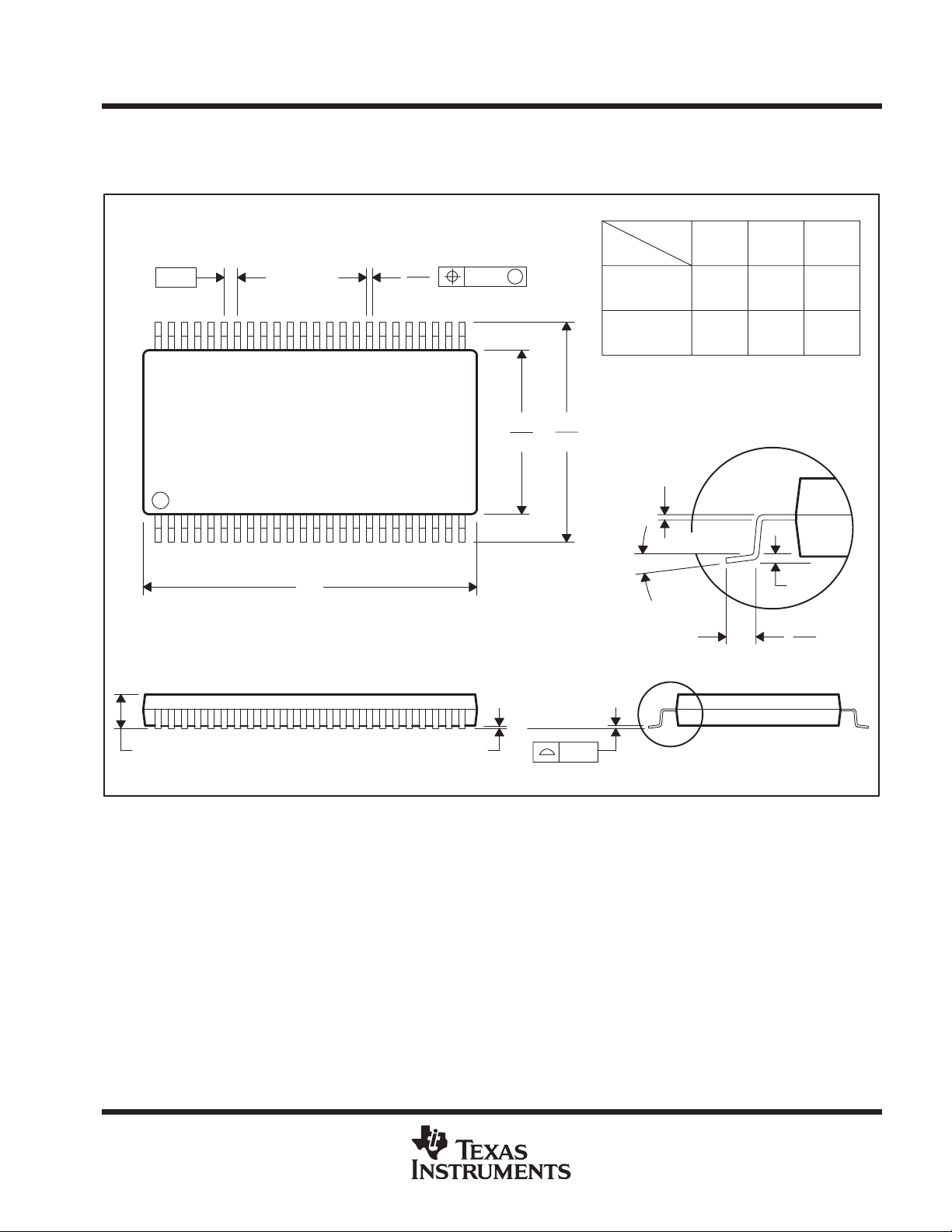
MECHANICAL INFORMATION
DGG (R-PDSO-G**) PLASTIC SMALL-OUTLINE PACKAGE
48 PIN SHOWN
48
1
0,50
PINS **
DIM
0,27
0,17
25
24
A
0,08
M
6,20
6,00
A MAX
A MIN
8,30
7,90
0,15 NOM
0°–8°
48
12,60
12,40
Gage Plane
56
14,10
13,90
64
17,10
16,90
0,25
0,75
0,50
1,20 MAX
NOTES: B. All linear dimensions are in millimeters.
C. This drawing is subject to change without notice.
D. Falls within JEDEC MO-153
0,05 MIN
Seating Plane
0,10
4040078/D 08/96
POST OFFICE BOX 655303 • DALLAS, TEXAS 75265
25

SN75976A, SN55976A
9-CHANNEL DIFFERENTIAL TRANSCEIVER
SLLS218B – MAY 1995 – REVISED MAY 1997
MECHANICAL INFORMATION
DL (R-PDSO-G**) PLASTIC SMALL-OUTLINE PACKAGE
48 PIN SHOWN
48
PINS **
DIM
A MAX
0.025 (0,635)
0.012 (0,305)
0.008 (0,203)
1
A
0.005 (0,13)
25
0.299 (7,59)
0.291 (7,39)
24
M
0.420 (10,67)
0.395 (10,03)
A MIN
0.006 (0,15) NOM
0°–8°
0.380
(9,65)
0.370
(9,40)
Gage Plane
4828
0.630
(16,00)
0.620
(15,75)
56
0.730
(18,54)
0.720
(18,29)
0.010 (0,25)
0.040 (1,02)
0.020 (0,51)
0.110 (2,79) MAX
NOTES: A. All linear dimensions are in inches (millimeters).
B. This drawing is subject to change without notice.
C. Body dimensions do not include mold flash or protrusion not to exceed 0.006 (0,15).
0.008 (0,20) MIN
Seating Plane
0.004 (0,10)
4040048/B 02/95
26
POST OFFICE BOX 655303 • DALLAS, TEXAS 75265

SN75976A, SN55976A
9-CHANNEL DIFFERENTIAL TRANSCEIVER
SLLS218B – MAY 1995 – REVISED MAY 1997
MECHANICAL INFORMATION
WD (R-GDFP-F**) CERAMIC DUAL FLATPACK
48 PIN SHOWN
0.120 (3,05)
0.075 (1,91)
0.005 (0,13) NOM
1.200 (30,50)
0.950 (24,13)
0.390 (9,91)
0.370 (9,40)
NO. OF
PINS**
48
56
481
MIN
0.630 0.730
(16,00)
0.610
(15,49)
A
MAX
(18,54)
0.710
(18,03)
0.025 (0,635)
A
24 25
NOTES: A. All linear dimensions are in inches (millimeters).
B. This drawing is subject to change without notice.
C. This package can be hermetically sealed with a ceramic lid using glass frit.
D. Index point is provided on cap for pin identification only
E. Falls within MIL-STD-1835: GDFP1-F48 and JEDEC MO-146AA
GDFP1-F56 and JEDEC MO-146AB
0.010 (0,25) TYP
4040176/C 04/96
POST OFFICE BOX 655303 • DALLAS, TEXAS 75265
27

IMPORTANT NOTICE
T exas Instruments (TI) reserves the right to make changes to its products or to discontinue any semiconductor
product or service without notice, and advises its customers to obtain the latest version of relevant information
to verify, before placing orders, that the information being relied on is current and complete.
TI warrants performance of its semiconductor products and related software to the specifications applicable at
the time of sale in accordance with TI’s standard warranty. Testing and other quality control techniques are
utilized to the extent TI deems necessary to support this warranty. Specific testing of all parameters of each
device is not necessarily performed, except those mandated by government requirements.
Certain applications using semiconductor products may involve potential risks of death, personal injury, or
severe property or environmental damage (“Critical Applications”).
TI SEMICONDUCTOR PRODUCTS ARE NOT DESIGNED, INTENDED, AUTHORIZED, OR WARRANTED
TO BE SUITABLE FOR USE IN LIFE-SUPPORT APPLICATIONS, DEVICES OR SYSTEMS OR OTHER
CRITICAL APPLICATIONS.
Inclusion of TI products in such applications is understood to be fully at the risk of the customer. Use of TI
products in such applications requires the written approval of an appropriate TI officer . Questions concerning
potential risk applications should be directed to TI through a local SC sales office.
In order to minimize risks associated with the customer’s applications, adequate design and operating
safeguards should be provided by the customer to minimize inherent or procedural hazards.
TI assumes no liability for applications assistance, customer product design, software performance, or
infringement of patents or services described herein. Nor does TI warrant or represent that any license, either
express or implied, is granted under any patent right, copyright, mask work right, or other intellectual property
right of TI covering or relating to any combination, machine, or process in which such semiconductor products
or services might be or are used.
Copyright 1998, Texas Instruments Incorporated
 Loading...