

DS8830, SN55183, SN75183
DUAL DIFFERENTIAL LINE DRIVERS
SLLS093D – OCTOBER 1972 – REVISED APRIL 1998
1
POST OFFICE BOX 655303 • DALLAS, TEXAS 75265
D
Single 5-V Supply
D
Differential Line Operation
D
Dual Channels
D
TTL Compatibility
D
Short-Circuit Protection of Outputs
D
Output Clamp Diodes to Terminate Line
Transients
D
High-Current Outputs
D
Quad Inputs
D
Single-Ended or Differential AND/NAND
Outputs
D
Designed for Use With Dual Differential
Drivers SN55182 and SN75182
D
Designed to Be Interchangeable With
National Semiconductor DS7830 and
DS8830
description
The DS8830, SN55183, and SN75183 dual
differential line drivers are designed to provide
differential output signals with high current
capability for driving balanced lines, such as
twisted pair, at normal line impedances without
high power dissipation. These devices can be
used as TTL expander/phase splitters, because
the output stages are similar to TTL totem-pole
outputs.
The driver is of monolithic single-chip construction, and both halves of the dual circuits use common power
supply and ground terminals.
The SN55183 is characterized for operation over the full military temperature range of –55°C to 125°C. The
DS8830 and SN75183 are characterized for operation from 0°C to 70°C.
Copyright 1998, Texas Instruments Incorporated
PRODUCTION DATA information is current as of publication date.
Products conform to specifications per the terms of Texas Instruments
standard warranty. Production processing does not necessarily include
testing of all parameters.
Please be aware that an important notice concerning availability, standard warranty, and use in critical applications of
Texas Instruments semiconductor products and disclaimers thereto appears at the end of this data sheet.
1
2
3
4
5
6
7
14
13
12
11
10
9
8
1A
1B
1C
1D
1Y
1Z
GND
V
CC
2D
2C
2B
2A
2Y
2Z
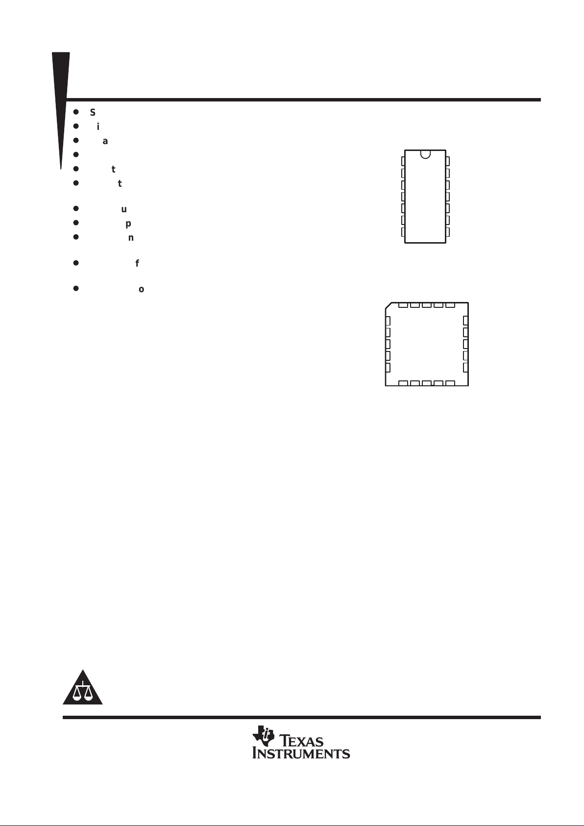
SN55183 ...J OR W PACKAGE
SN75183 ...D OR N PACKAGE
DS8830 ... N PACKAGE
(TOP VIEW)
3 2 1 20 19
910111213
4
5
6
7
8
18
17
16
15
14
2C
NC
2B
NC
2A
1C
NC
1D
NC
1Y
SN55183 . . . FK PACKAGE
(TOP VIEW)
1B1ANC
2Z
2Y
2D
1Z
GND
NC
CC
V
THE DS8830 AND SN55183 ARE
NOT RECOMMENDED FOR NEW DESIGNS
NC – No internal connection
DS8830, SN55183, SN75183
DUAL DIFFERENTIAL LINE DRIVERS
SLLS093D – OCTOBER 1972 – REVISED APRIL 1998
2
POST OFFICE BOX 655303 • DALLAS, TEXAS 75265
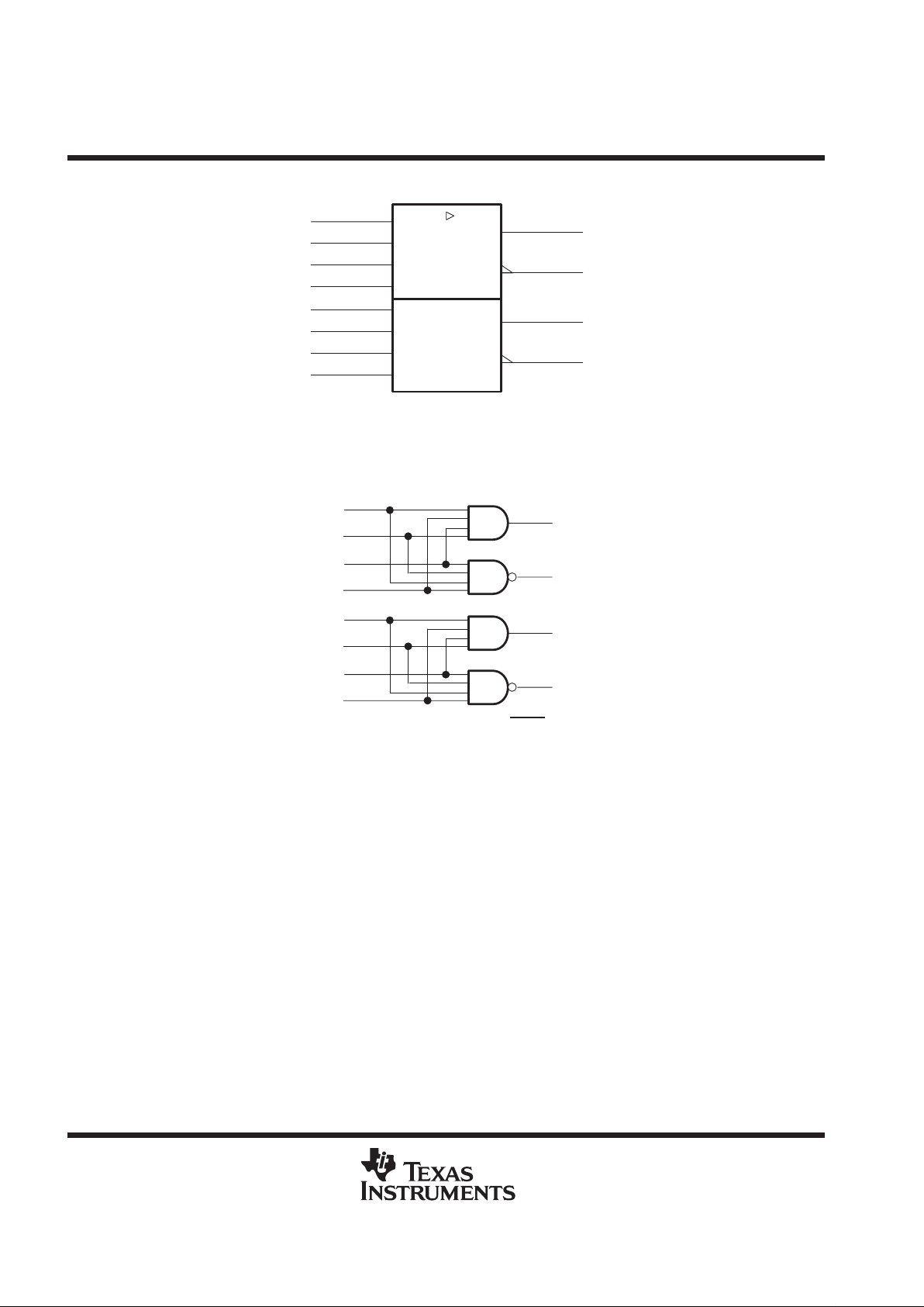
logic symbol
†
†
This symbol is in accordance with ANSI/IEEE Std 91-1984 and IEC Publication 617-12.
Pin numbers shown are for the D, J, N, and W packages.
&
1Z
6
2Z
8
1
1A
2
1B
3
1C
4
1D
1Y
5
10
2A
11
2B
12
2C
13
2D
2Y
9
logic diagram (positive logic)
1Y
5
Pin numbers shown are for the D, J, N, and W packages.
1
2
3
4
6
1Z
1A
1B
1C
1D
2Y
9
10
11
12
13
8
2Z
2A
2B
2C
2D
Positive logic: y = ABCD, Z = ABCD
DS8830, SN55183, SN75183
DUAL DIFFERENTIAL LINE DRIVERS
SLLS093D – OCTOBER 1972 – REVISED APRIL 1998
3
POST OFFICE BOX 655303 • DALLAS, TEXAS 75265
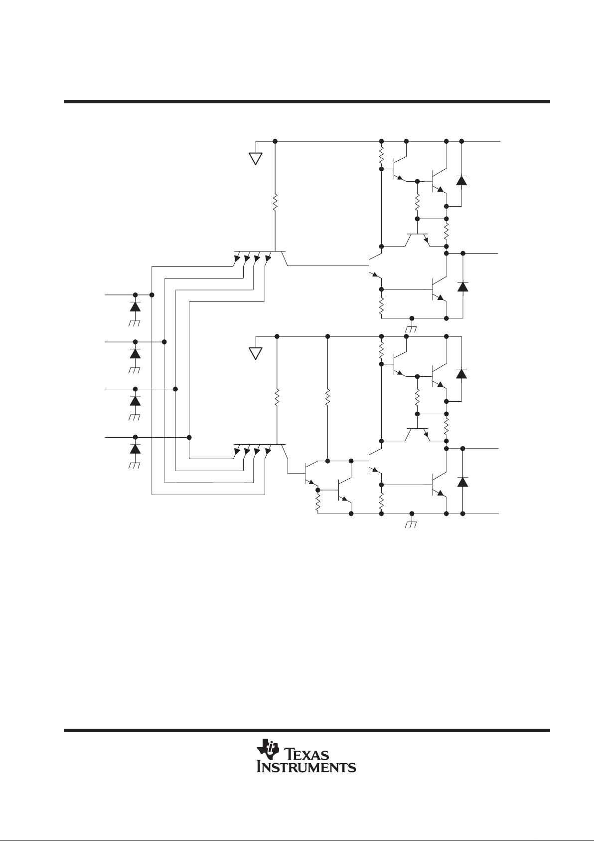
schematic (each driver)
A
B
C
D
4 kΩ 3.2 kΩ
GND
Y
9 Ω
300 Ω
Z
V
CC
3 kΩ
545 Ω
2 kΩ
545 Ω
3 kΩ
300 Ω
2 kΩ
9 Ω
V
V
1, 10
14
2, 11
3, 12
4, 13
6, 8
5, 9
7
Resistor values shown are nominal.
Pin numbers shown are for the D, J, N, and W packages.

DS8830, SN55183, SN75183
DUAL DIFFERENTIAL LINE DRIVERS
SLLS093D – OCTOBER 1972 – REVISED APRIL 1998
4
POST OFFICE BOX 655303 • DALLAS, TEXAS 75265
absolute maximum ratings over operating free-air temperature range (unless otherwise noted)
†
Supply voltage, V
CC
(see Note 1) 7 V. . . . . . . . . . . . . . . . . . . . . . . . . . . . . . . . . . . . . . . . . . . . . . . . . . . . . . . . . . . . .
Input voltage, V
I
5.5 V. . . . . . . . . . . . . . . . . . . . . . . . . . . . . . . . . . . . . . . . . . . . . . . . . . . . . . . . . . . . . . . . . . . . . . . . . .
Duration of output short circuit (see Note 2) 1 s. . . . . . . . . . . . . . . . . . . . . . . . . . . . . . . . . . . . . . . . . . . . . . . . . . . .
Continuous total power dissipation See Dissipation Rating Table. . . . . . . . . . . . . . . . . . . . . . . . . . . . . . . . . . . . .
Storage temperature range, T
stg
–65°C to 150°C. . . . . . . . . . . . . . . . . . . . . . . . . . . . . . . . . . . . . . . . . . . . . . . . . . .
Lead temperature 1,6 mm (1/16 inch) from case for 10 seconds: D or N package 260°C. . . . . . . . . . . . . . . .
Lead temperature 1,6 mm (1/16 inch) from case for 60 seconds: J package 300°C. . . . . . . . . . . . . . . . . . . . .
Case temperature for 60 seconds, T
c
: FK package 260°C. . . . . . . . . . . . . . . . . . . . . . . . . . . . . . . . . . . . . . . . . . .
†
Stresses beyond those listed under “absolute maximum ratings” may cause permanent damage to the device. These are stress ratings only, and
functional operation of the device at these or any other conditions beyond those indicated under “recommended operating conditions” is not
implied. Exposure to absolute-maximum-rated conditions for extended periods may affect device reliability.
NOTES: 1. All voltage values, except differential voltages, are with respect to network ground terminal.
2. Not more than one output should be shorted to ground at any one time.
DISSIPATION RATING TABLE
PACKAGE
TA ≤ 25°C
POWER RATING
DERATING FACTOR
ABOVE TA = 25°C
TA = 70°C
POWER RATING
TA = 125°C
POWER RATING
D 950 mW 7.6 mW/°C 608 mW –
FK
‡
1375 mW 11.0 mW/°C 880 mW 275 mW
J
‡
1375 mW 11.0 mW/°C 880 mW 275 mW
N 1150 mW 9.2 mW/°C 736 mW –
W
‡
1000 mW 8.0 mW/°C 640 mW 200 mW
‡
In the FK, J, and W packages, SN55183 chips are alloy mounted and SN75183 chips are glass mounted.
recommended operating conditions
SN55183
DS8830,
SN75183
UNIT
MIN NOM MAX MIN NOM MAX
Supply voltage, V
CC
4.5 5 5.5 4.75 5 5.25 V
High-level input voltage, V
IH
2 2 V
Low-level input voltage, V
IL
0.8 0.8 V
High-level output current, I
OH
–40 –40 mA
Low-level output current, I
OL
40 40 mA
Operating free-air temperature, T
A
–55 125 0 70 °C

DS8830, SN55183, SN75183
DUAL DIFFERENTIAL LINE DRIVERS
SLLS093D – OCTOBER 1972 – REVISED APRIL 1998
5
POST OFFICE BOX 655303 • DALLAS, TEXAS 75265
electrical characteristics over recommended ranges of VCC and operating free-air temperature
(unless otherwise noted)
PARAMETER TEST CONDITIONS MIN TYP†MAX UNIT
p
p
IOH = –0.8 mA 2.4
VOHHigh-level output voltage
Y (AND) outputs
V
IH
= 2
V
IOH = –40 mA 1.8 3.3
V
p
p
IOL = 32 mA 0.2
VOLLow-level output voltage
Y (AND) outputs
V
IL
= 0.8
V
IOL = 40 mA 0.22 0.4
V
p
p
IOH = –0.8 mA 2.4
VOHHigh-level output voltage
Z (NAND) outputs
V
IL
= 0.8
V
IOH = –40 mA 1.8 3.3
V
p
p
IOL = 32 mA 0.2
VOLLow-level output voltage
Z (NAND) outputs
V
IH
= 2
V
IOL = 40 mA 0.22 0.4
V
I
IH
High-level input current VIH = 2.4 V 120 µA
I
I
Input current at maximum input voltage VIH = 5.5 V 2 mA
I
IL
Low-level input current VIL = 0.4 V –4.8 mA
I
OS
Short-circuit output current
‡
VCC = 5 V, TA =125°C
§
–40 –100 –120 mA
I
CC
Supply current (average per driver) VCC = 5 V, All inputs at 5 V, No load 10 18 mA
†
All typical values are at VCC = 5 V, TA = 25°C.
‡
Not more than one output should be shorted to ground at a time, and duration of the short circuit should not exceed one second.
§
TA = 125°C is applicable to SN55183 only.
switching characteristics, VCC = 5 V, TA = 25°C
PARAMETER TEST CONDITIONS MIN TYP MAX UNIT
t
PLH
Propagation delay time, low- to high-level Y output AND gates
CL = 15 pF,
See FIgure 1(a)
8 12 ns
t
PHL
Propagation delay time, high- to low-level Y output AND gates
CL = 15 pF,
See FIgure 1(a)
12 18 ns
t
PLH
Propagation delay time, low- to high-level Z output NAND gates
CL = 15 pF,
See FIgure 1(a)
6 12 ns
t
PHL
Propagation delay time, high- to low-level Z output NAND gates
CL = 15 pF,
See FIgure 1(a)
6 8 ns
t
PLH
Propagation delay time,
low- to high-level differential output
Y output with respect to Z output,
RL = 100 Ω in series with 5000 pF,
See Figure 1(b)
9 16 ns
t
PHL
Propagation delay time,
high- to low-level differential output
Y output with respect to Z output,
RL = 100 Ω in series with 5000 pF,
See Figure 1(b)
8 16 ns

DS8830, SN55183, SN75183
DUAL DIFFERENTIAL LINE DRIVERS
SLLS093D – OCTOBER 1972 – REVISED APRIL 1998
6
POST OFFICE BOX 655303 • DALLAS, TEXAS 75265
PARAMETER MEASUREMENT INFORMATION
(a) OUTPUTS Y AND Z
Differential
Output
Voltage
VOLTAGE WA VEFORMS
3 V
V
YS
0 V
–V
YS
0 V
1.5 V1.5 V
Input
t
PHL
t
PLH
VOLTAGE WA VEFORMS
V
OL
V
OH
V
OL
V
OH
0 V
2.5 V
1.5 V
1.5 V
1.5 V
t
PLH
t
PHL
t
PHL
1.5 V
1.5 V
t
PLH
1.5 V
Input
Input
VCC = 5 V
5000 pF
100
W
TEST CIRCUIT
TEST CIRCUIT
CL = 15 pF
(see Note B)
Z
Output
CL = 15 pF
(see Note B)
Y
Output
VCC = ±5 V
Input
Pulse
Generator
(see Note A)
(b) DIFFERENTIAL OUTPUT
Y
Output
Z
Output
Pulse
Generator
(see Note A)
Z
Output
Y
Output
0 V
NOTES: A. The pulse generators have the following characteristics: ZO = 50 Ω, tr ≤ 10 ns, tf ≤ 10 ns, tw = 0.5 µs, PRR ≤ 1 MHz.
B. CL includes probe and jig capacitance.
C. Waveforms are monitored on an oscilloscope with ri ≥ 1 MΩ.
Figure 1. Test Circuits and Voltage Waveforms

DS8830, SN55183, SN75183
DUAL DIFFERENTIAL LINE DRIVERS
SLLS093D – OCTOBER 1972 – REVISED APRIL 1998
7
POST OFFICE BOX 655303 • DALLAS, TEXAS 75265
TYPICAL CHARACTERISTICS
†
Figure 2
– Input Threshold Voltage – V
INPUT THRESHOLD VOLTAGE
vs
FREE-AIR TEMPERATURE
TA – Free-Air Temperature – °C
VCC = 5 V
VO = 1.5 V
VIL max
AND Gate
NAND Gate
VIH min
V
T
2.4
2.2
2
1.8
1.6
1.4
1.2
1
0.8
0.6
0.4
–75 –50 –25 0 25 50 75 100 125
Figure 3
– High-Level Output Voltage – V
HIGH-LEVEL OUTPUT VOLTAGE
vs
HIGH-LEVEL OUTPUT CURRENT
50-Ω Load
IOH – High-Level Output Current – mA
TA = 125°C
TA = – 55°C
TA = 25°C
200-Ω Load
VCC = 5 V
V
OH
100-Ω Load
4
3.5
3
2.5
2
1.5
1
0.5
0
–20 –40 –60 –80 –100 –120 –140 –1600
Figure 4
– Differential Output Voltage – V
DIFFERENTIAL OUTPUT VOLTAGE
vs
DIFFERENTIAL OUTPUT CURRENT
TA = 125°C
IOD – Differential Output Current – mA
V
OD
TA = 25°C
ÏÏÏÏ
VCC = 5 V
TA = –55°C
4
3
2
1
0
25 50 75 100 1250
Figure 5
– Low-Level Output Voltage – V
LOW-LEVEL OUTPUT VOLTAGE
vs
LOW-LEVEL OUTPUT CURRENT
IOL – Low-Level Output Current – mA
TA = –55°C
TA = 125°C
TA = 25°C
VCC = 5 V
V
OL
3
2
1
0
40 80 120 160 2000 20 60 100 140 180
†
Operation of the device at these or any other conditions beyond those indicated under “recommended operating conditions” is not implied.

DS8830, SN55183, SN75183
DUAL DIFFERENTIAL LINE DRIVERS
SLLS093D – OCTOBER 1972 – REVISED APRIL 1998
8
POST OFFICE BOX 655303 • DALLAS, TEXAS 75265
TYPICAL CHARACTERISTICS
†
Figure 6
TA – Free-Air Temperature – °C
– Propagation Delay Time – ns
PROPAGATION DELAY TIME
(DIFFERENTIAL OUTPUT)
vs
FREE-AIR TEMPERATURE
VCC = 5 V
See Figure 1(b)
t
PHL
t
PLH
t
pd
20
15
10
5
0
–50 –25 0 25 125–75 1007550
Figure 7
– Total Power Dissipation – mW
TOTAL POWER DISSIPATION
(BOTH DRIVERS)
vs
FREQUENCY
f – Frequency – MHz
P
D
VCC = 5 V
No Load
Input: 3-V Square Wave
TA = 25°C
240
220
200
180
160
140
120
100
80
60
40
0.1 10.4 4 10 40 100
†
Operation of the device at these or any other conditions beyond those indicated under “recommended operating conditions” is not implied.

DS8830, SN55183, SN75183
DUAL DIFFERENTIAL LINE DRIVERS
SLLS093D – OCTOBER 1972 – REVISED APRIL 1998
9
POST OFFICE BOX 655303 • DALLAS, TEXAS 75265
APPLICATION INFORMATION
Twisted
Pair
Resp Time Cont
Output
100 pF
(see Note B)
Noninverting
Input Strobe
0.002 µF
(see Note A)
1/2 ’182
VCC = 5 V
GND
Y
Z
GND
VCC = 5 V
1/2 ’183
Inputs
D
C
B
A
R
T
NOTES: A. When the inputs are open circuited, the output is high. A capacitor may be used for dc isolation of the line-terminating resistor.
At the frequency of operation, the impedance of the capacitor should be relatively small.
B. Use of a capacitor to control response time is optional.
Example: let f = 5 MHz
C = 0.002 µF
Z
(
circuit
)
[16W
Z
(
circuit
)
+
1
2pfC
+
1
2
p
ǒ
5 10
6
Ǔǒ
0.002 10
*
6
Ǔ
Inverting
Input
Figure 8. Transmission of Digital Data Over Twisted-Pair Line

IMPORTANT NOTICE
T exas Instruments and its subsidiaries (TI) reserve the right to make changes to their products or to discontinue
any product or service without notice, and advise customers to obtain the latest version of relevant information
to verify, before placing orders, that information being relied on is current and complete. All products are sold
subject to the terms and conditions of sale supplied at the time of order acknowledgement, including those
pertaining to warranty, patent infringement, and limitation of liability.
TI warrants performance of its semiconductor products to the specifications applicable at the time of sale in
accordance with TI’s standard warranty. Testing and other quality control techniques are utilized to the extent
TI deems necessary to support this warranty. Specific testing of all parameters of each device is not necessarily
performed, except those mandated by government requirements.
CERT AIN APPLICATIONS USING SEMICONDUCTOR PRODUCTS MAY INVOLVE POTENTIAL RISKS OF
DEATH, PERSONAL INJURY, OR SEVERE PROPERTY OR ENVIRONMENTAL DAMAGE (“CRITICAL
APPLICATIONS”). TI SEMICONDUCTOR PRODUCTS ARE NOT DESIGNED, AUTHORIZED, OR
WARRANTED TO BE SUITABLE FOR USE IN LIFE-SUPPORT DEVICES OR SYSTEMS OR OTHER
CRITICAL APPLICATIONS. INCLUSION OF TI PRODUCTS IN SUCH APPLICA TIONS IS UNDERST OOD TO
BE FULLY AT THE CUSTOMER’S RISK.
In order to minimize risks associated with the customer’s applications, adequate design and operating
safeguards must be provided by the customer to minimize inherent or procedural hazards.
TI assumes no liability for applications assistance or customer product design. TI does not warrant or represent
that any license, either express or implied, is granted under any patent right, copyright, mask work right, or other
intellectual property right of TI covering or relating to any combination, machine, or process in which such
semiconductor products or services might be or are used. TI’s publication of information regarding any third
party’s products or services does not constitute TI’s approval, warranty or endorsement thereof.
Copyright 1998, Texas Instruments Incorporated
 Loading...