

SN54F621, SN74F621
OCTAL BUS TRANSCEIVERS
WITH OPEN-COLLECTOR OUTPUTS
SDFS004B – D2932, MARCH 1987 – REVISED OCTOBER 1993
Copyright 1993, Texas Instruments Incorporated
2–1
POST OFFICE BOX 655303 • DALLAS, TEXAS 75265
• Local Bus-Latch Capability
• Noninverting Logic
• Package Options Include Plastic
Small-Outline Packages, Ceramic Chip
Carriers, and Standard Plastic and Ceramic
300-mil DIPs
description
These octal bus transceivers are designed for
asynchronous communication between data
buses. The control function implementation allows
for maximum flexibility in timing.
These devices allow data transmission from the A
bus to the B bus or from the B bus to the A bus
depending upon the logic levels at the output
enable (OEAB and OEBA
) inputs.
The output-enable inputs can be used to disable
the device so that the buses are effectively
isolated. The dual-enable configuration gives the
transceivers the capability of storing data by
simultaneously enabling OEAB and OEBA
. Each
output reinforces its input in this configuration.
When both OEAB and OEBA
are enabled and all
other data sources to the two sets of bus lines are
at high impedance, both sets of bus lines (16 in all)
will remain at their last states.
The SN54F621 is characterized for operation over
the full military temperature range of –55°C to
125°C. The SN74F621 is characterized for
operation from 0°C to 70°C.
FUNCTION TABLE
INPUTS
OEBA OEAB
OPERATION
L L B data to A bus
L H
B data to A bus,
A data to B bus
H L Isolation
H H A data to B bus
1
2
3
4
5
6
7
8
9
10
20
19
18
17
16
15
14
13
12
11
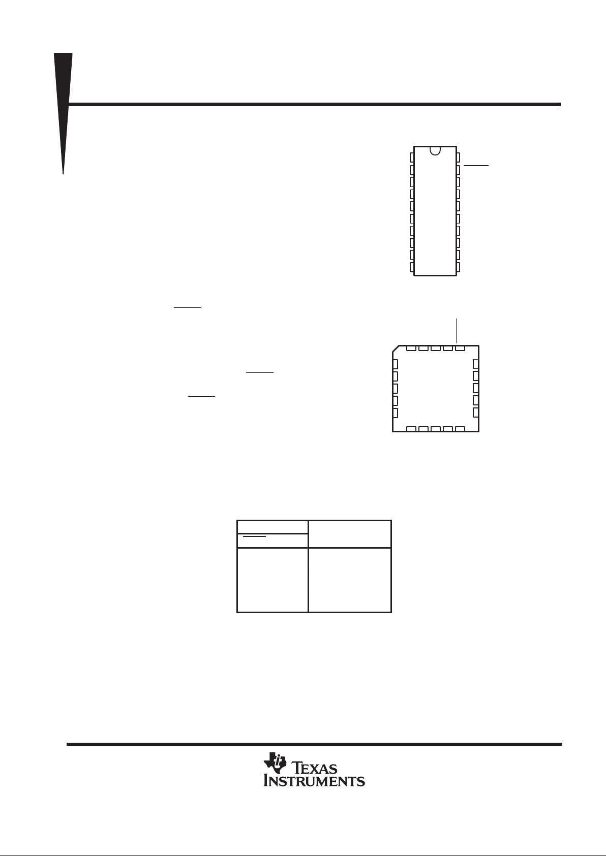
OEAB
A1
A2
A3
A4
A5
A6
A7
A8
GND
V
CC
OEBA
B1
B2
B3
B4
B5
B6
B7
B8
SN54F621 ...J PACKAGE
SN74F621 . . . DW OR N PACKAGE
(TOP VIEW)
3 2 1 20 19
9 10 11 12 13
4
5
6
7
8
18
17
16
15
14
B1
B2
B3
B4
B5
A3
A4
A5
A6
A7
SN54F621 . . . FK PACKAGE
(TOP VIEW)
A2A1OEAB
B7
B6
OEBA
A8
GND
B8
V
CC
PRODUCTION DATA information is current as of publication date.
Products conform to specifications per the terms of Texas Instruments
standard warranty. Production processing does not necessarily include
testing of all parameters.
SN54F621, SN74F621
OCTAL BUS TRANSCEIVERS
WITH OPEN-COLLECTOR OUTPUTS
SDFS004B – D2932, MARCH 1987 – REVISED OCTOBER 1993
2–2
POST OFFICE BOX 655303 • DALLAS, TEXAS 75265
logic symbol
†
logic diagram (positive logic)
2
A1 B1
EN1
19
EN2
1
OEAB
2
A1
3
A2
B1
18
4
A3
5
A4
6
A5
7
A6
8
A7
9
A8
B2
17
B3
16
B5
14
B4
15
B6
13
B8
11
B7
12
OEBA
1
OEBA
OEAB
19
1
182
To Seven Other Channels
†
This symbol is in accordance with ANSI/IEEE Std 91-1984 and
IEC Publication 617-12.
absolute maximum ratings over operating free-air temperature range (unless otherwise noted)
‡
Supply voltage range, V
CC
–0.5 V to 7 V. . . . . . . . . . . . . . . . . . . . . . . . . . . . . . . . . . . . . . . . . . . . . . . . . . . . . . . . . .
Input voltage range, V
I
(excluding I/O ports) (see Note 1) –1.2 V to 7 V. . . . . . . . . . . . . . . . . . . . . . . . . . . . . . . .
Input current range, I
IK
–30 mA to 5 mA. . . . . . . . . . . . . . . . . . . . . . . . . . . . . . . . . . . . . . . . . . . . . . . . . . . . . . . . . . . .
Voltage range applied to any output in the high state –0.5 V to 5.5 V. . . . . . . . . . . . . . . . . . . . . . . . . . . . . . . . . . .
Current into any output in the low state: SN54F621 (A1–A8) 40 mA. . . . . . . . . . . . . . . . . . . . . . . . . . . . . . . . . . .
SN54F621 (B1–B8) 96 mA. . . . . . . . . . . . . . . . . . . . . . . . . . . . . . . . . . .
SN74F621 (A1–A8) 48 mA. . . . . . . . . . . . . . . . . . . . . . . . . . . . . . . . . . .
SN74F621 (B1–B8) 128 mA. . . . . . . . . . . . . . . . . . . . . . . . . . . . . . . . . .
Operating free-air temperature range: SN54F621 –55°C to 125°C. . . . . . . . . . . . . . . . . . . . . . . . . . . . . . . . . . .
SN74F621 0°C to 70°C. . . . . . . . . . . . . . . . . . . . . . . . . . . . . . . . . . . . . . .
Storage temperature range –65°C to 150°C. . . . . . . . . . . . . . . . . . . . . . . . . . . . . . . . . . . . . . . . . . . . . . . . . . . . . . . .
‡
Stresses beyond those listed under “absolute maximum ratings” may cause permanent damage to the device. These are stress ratings only, and
functional operation of the device at these or any other conditions beyond those indicated under “recommended operating conditions” is not
implied. Exposure to absolute-maximum-rated conditions for extended periods may affect device reliability.
NOTE 1: The input-voltage ratings may be exceeded provided the input-current ratings are observed.
recommended operating conditions
SN54F621 SN74F621
MIN NOM MAX MIN NOM MAX
UNIT
V
CC
Supply voltage 4.5 5 5.5 4.5 5 5.5 V
V
IH
High-level input voltage 2 2 V
V
OH
High-level output voltage 5.5 5.5 V
V
IL
Low-level input voltage 0.8 0.8 V
I
IK
Input clamp current –18 –18 mA
p
A1–A8 20 24
IOLLow-level output current
B1–B8 48 64
mA
T
A
Operating free-air temperature –55 125 0 70 °C
 Loading...